EP3537848B1 - Switching sub-system for distributed antenna systems using time division duplexing - Google Patents
Switching sub-system for distributed antenna systems using time division duplexing Download PDFInfo
- Publication number
- EP3537848B1 EP3537848B1 EP19171578.8A EP19171578A EP3537848B1 EP 3537848 B1 EP3537848 B1 EP 3537848B1 EP 19171578 A EP19171578 A EP 19171578A EP 3537848 B1 EP3537848 B1 EP 3537848B1
- Authority
- EP
- European Patent Office
- Prior art keywords
- downlink
- uplink
- clock setting
- switching
- signal power
- Prior art date
- Legal status (The legal status is an assumption and is not a legal conclusion. Google has not performed a legal analysis and makes no representation as to the accuracy of the status listed.)
- Active
Links
- 238000005259 measurement Methods 0.000 claims description 48
- 238000000034 method Methods 0.000 claims description 27
- 238000004891 communication Methods 0.000 claims description 25
- 230000006870 function Effects 0.000 claims description 5
- 238000005070 sampling Methods 0.000 claims 2
- 230000003287 optical effect Effects 0.000 description 16
- 230000008569 process Effects 0.000 description 16
- 238000009826 distribution Methods 0.000 description 14
- 230000005540 biological transmission Effects 0.000 description 9
- 238000010586 diagram Methods 0.000 description 6
- 238000012545 processing Methods 0.000 description 4
- 230000008878 coupling Effects 0.000 description 2
- 238000010168 coupling process Methods 0.000 description 2
- 238000005859 coupling reaction Methods 0.000 description 2
- 230000007246 mechanism Effects 0.000 description 2
- RYGMFSIKBFXOCR-UHFFFAOYSA-N Copper Chemical compound [Cu] RYGMFSIKBFXOCR-UHFFFAOYSA-N 0.000 description 1
- 230000006978 adaptation Effects 0.000 description 1
- 230000000903 blocking effect Effects 0.000 description 1
- 238000006243 chemical reaction Methods 0.000 description 1
- 229910052802 copper Inorganic materials 0.000 description 1
- 239000010949 copper Substances 0.000 description 1
- 230000007812 deficiency Effects 0.000 description 1
- 238000001514 detection method Methods 0.000 description 1
- 238000002955 isolation Methods 0.000 description 1
- 238000012986 modification Methods 0.000 description 1
- 230000004048 modification Effects 0.000 description 1
- 239000013307 optical fiber Substances 0.000 description 1
- 230000004044 response Effects 0.000 description 1
- 238000012552 review Methods 0.000 description 1
- 230000003068 static effect Effects 0.000 description 1
- 230000000007 visual effect Effects 0.000 description 1
Images


Classifications
-
- H—ELECTRICITY
- H04—ELECTRIC COMMUNICATION TECHNIQUE
- H04J—MULTIPLEX COMMUNICATION
- H04J3/00—Time-division multiplex systems
- H04J3/02—Details
- H04J3/06—Synchronising arrangements
- H04J3/0635—Clock or time synchronisation in a network
- H04J3/0638—Clock or time synchronisation among nodes; Internode synchronisation
-
- H—ELECTRICITY
- H04—ELECTRIC COMMUNICATION TECHNIQUE
- H04L—TRANSMISSION OF DIGITAL INFORMATION, e.g. TELEGRAPHIC COMMUNICATION
- H04L5/00—Arrangements affording multiple use of the transmission path
- H04L5/14—Two-way operation using the same type of signal, i.e. duplex
- H04L5/1469—Two-way operation using the same type of signal, i.e. duplex using time-sharing
-
- H—ELECTRICITY
- H04—ELECTRIC COMMUNICATION TECHNIQUE
- H04B—TRANSMISSION
- H04B7/00—Radio transmission systems, i.e. using radiation field
- H04B7/02—Diversity systems; Multi-antenna system, i.e. transmission or reception using multiple antennas
- H04B7/022—Site diversity; Macro-diversity
- H04B7/024—Co-operative use of antennas of several sites, e.g. in co-ordinated multipoint or co-operative multiple-input multiple-output [MIMO] systems
-
- H—ELECTRICITY
- H04—ELECTRIC COMMUNICATION TECHNIQUE
- H04W—WIRELESS COMMUNICATION NETWORKS
- H04W24/00—Supervisory, monitoring or testing arrangements
- H04W24/02—Arrangements for optimising operational condition
-
- H—ELECTRICITY
- H04—ELECTRIC COMMUNICATION TECHNIQUE
- H04W—WIRELESS COMMUNICATION NETWORKS
- H04W72/00—Local resource management
- H04W72/04—Wireless resource allocation
- H04W72/044—Wireless resource allocation based on the type of the allocated resource
- H04W72/0446—Resources in time domain, e.g. slots or frames
-
- H—ELECTRICITY
- H04—ELECTRIC COMMUNICATION TECHNIQUE
- H04W—WIRELESS COMMUNICATION NETWORKS
- H04W88/00—Devices specially adapted for wireless communication networks, e.g. terminals, base stations or access point devices
- H04W88/08—Access point devices
- H04W88/085—Access point devices with remote components
-
- H—ELECTRICITY
- H04—ELECTRIC COMMUNICATION TECHNIQUE
- H04B—TRANSMISSION
- H04B7/00—Radio transmission systems, i.e. using radiation field
- H04B7/02—Diversity systems; Multi-antenna system, i.e. transmission or reception using multiple antennas
- H04B7/022—Site diversity; Macro-diversity
-
- H—ELECTRICITY
- H04—ELECTRIC COMMUNICATION TECHNIQUE
- H04J—MULTIPLEX COMMUNICATION
- H04J3/00—Time-division multiplex systems
- H04J3/02—Details
- H04J3/06—Synchronising arrangements
- H04J3/0635—Clock or time synchronisation in a network
- H04J3/0685—Clock or time synchronisation in a node; Intranode synchronisation
Definitions
- the present disclosure relates generally to telecommunication systems and more particularly (although not necessarily exclusively) to switching sub-systems for distributed antenna systems using time division duplexing.
- Telecommunications operators use telecommunication systems to provide signal coverage to coverage zones in which wireless devices are located.
- a distributed system may be used to extend the coverage of such telecommunication systems.
- distributed antenna systems include signal paths between base stations or other signal sources operated by telecommunication operators and remote antenna units positioned in one or more geographical coverage areas.
- a DAS may be configured for time division duplexing ("TDD") operations in which downlink and uplink signals are respectively transmitted and received using at least some common frequencies or common portions of a signal path.
- TDD time division duplexing
- a DAS configured for TDD operations may include one or more switches for isolating downlink signal paths from uplink signal paths.
- multiple telecommunication operators may use the same DAS for extending the coverage of their respective telecommunication systems.
- An entity responsible for configuring or otherwise operating the DAS may be independent of the telecommunication operators that use the DAS.
- the entity being independent of the telecommunication operators may present disadvantages. For example, it may be difficult or infeasible to configure the switching operations of the DAS in accordance with the TDD configuration used by the telecommunication operators.
- US 2009/316611 A1 discloses a method of determining a boundary of a subframe in a time division duplexing (TDD) system.
- a power level of a signal on at least one radio frequency is detected, the signal comprising at least one subframe.
- a time domain correlation is done on the detected signal with a first reference signal, wherein the first reference signal represents at least one subframe.
- the location and time of a boundary of the at least one subframe of the detected signal is determined based on the correlation of the detected signal and the first reference signal.
- Certain aspects and examples are directed to switching sub-systems for a distributed antenna system ("DAS") configured for time division duplexing (“TDD”) operations.
- DAS distributed antenna system
- TDD time division duplexing
- the DAS can use a switching sub-system to switch between an uplink mode for communicating TDD signals in an uplink direction and a downlink mode for communicating TDD signals in a downlink direction.
- the switching sub-system can automatically determine switching times for the DAS based on determining whether a signal level for downlink signals exceeds a threshold level.
- One or more switches of the switching sub-system can switch a remote antenna unit of the DAS to the downlink mode by selectively connecting one or more components of the downlink path in the remote antenna unit and disconnecting one or more components of a corresponding uplink path in the remote antenna unit.
- the switching sub-system can include a switching control module that detects the downlink/uplink ratio of base stations in communication with the DAS.
- the switching control module can determine an initial clock setting based on the downlink/uplink ratio.
- the initial clock setting can determine the timing for sending command signals to the switches of the switching sub-system that instruct the switches to switch the DAS between an uplink mode and a downlink mode.
- the switching control module can also optimize a clock setting that controls switching times for the switches. Optimizing the switching times can maximize or otherwise improve data throughput via the DAS.
- the switching control module can optimize the clock setting by determining start or end times for respective downlink subframes transmitted via the downlink path.
- the switching control module can determine the start or end times based on when signal power measurements for the downlink path exceed a threshold signal power.
- the switching control module can statistically determine a switching time adjustment based on a set of switching time differentials between the initial clock setting and the determined start or end times for the downlink sub-frames. For example, the switching time adjustment may be the statistical mean of the set of switching time differentials.
- the switching control module can update the clock setting based on the switching time adjustment.
- the switching control module can be used to automatically determine a TDD configuration for one or more telecommunication operators using the DAS. Automatically determining the TDD configuration can reduce or eliminate the need for manual configuration of the DAS with respect to each telecommunication operator. Reducing or eliminating the need for manual configuration of the DAS can reduce or avoid problems resulting from missing information with respect to the configuration settings of different telecommunication operators.
- the switching control module can also compensate for uplink or downlink pulsing variation or other deficiencies components of the DAS in the uplink or downlink direction, such as a jitter or clock frequency drift experienced by one or more reference clock devices in the DAS.
- FIG. 1 is a block diagram depicting an example of DAS 100 having a TDD switching sub-system 110 according to one aspect.
- the DAS 100 can include a master unit 102 in communication with remote antenna units 104a, 104b and with base stations 101a, 101b.
- different base stations can communicate signals associated with different telecommunication operators.
- the DAS 100 can be positioned in a geographical area (e.g., a stadium, an office building, etc.) to extend wireless communication coverage of the base stations 101a, 101b into geographical coverage areas 108a, 108b.
- a geographical area e.g., a stadium, an office building, etc.
- the DAS 100 or other telecommunication system can include downlink paths for transporting downlink signals from the base stations 101a, 101b to one or more of the remote antenna units 104a, 104b.
- the DAS 100 can receive downlink signals from the base stations 101a, 101b via a wired or wireless communication medium. Downlink signals can include signals provided from the base stations 101a, 101b and transmitted by the remote antenna units 104a, 104b in the coverage areas 108a, 108b.
- a non-limiting example of a remote antenna unit is a universal access point.
- the DAS 100 or other telecommunication system can also include uplink paths for transporting uplink signals from one or more of the remote antenna units 104a, 104b to one of more of the base stations or repeaters.
- Uplink signals are signals at frequencies in an uplink frequency band that are recovered or otherwise received by one or more of the remote antenna units 104a, 104b from communication devices in the coverage areas 108a, 108b.
- the master unit 102 can communicate signals between the base stations 101a, 101b and the remote antenna units 104a, 104b.
- An example of a master unit 102 is a wireless conversion station.
- the master unit 102 and remote antenna unit(s) 104a, 104b can communicate via any suitable communication medium.
- the communication medium can be any suitable medium for providing a serial communication link between the master unit 102 and the remote antenna unit 104a, 104b.
- the communication medium can be an optical fiber.
- the communication medium can include copper cables, microwave links, etc.
- the master unit 102 and remote antenna units 104a, 104b can include analog-to- digital and digital-to-analog converters for digital communication over a serial link.
- FIG. 1 depicts a single master unit 102 in communication with two base stations 101a, 101b and two remote antenna units 104a, 104b.
- a distributed antenna system 100 can include any number of master units and any number of remote antenna units for communicating signals between any number of base stations or other signal sources and any number of coverage areas.
- a DAS 100 can include other devices in addition to master units, remote antenna units, and extension units.
- the DAS 100 may include a base station router or other interface device that receives signals from base stations 101a, 101b and provides the signals to the master unit 102.
- the DAS 100 may include one or more extension units that communicate signals between the master unit 102 and the remote antenna units 104a, 104b.
- the DAS 100 can be configured for TDD operations that support multiple operators communicating signals via the DAS 100.
- the DAS 100 can switch between an uplink mode for communicating TDD signals in an uplink direction and a downlink mode for communicating TDD signals in a downlink direction.
- the remote antenna units 104a, 104b can respectively include TDD switching sub-systems 110a, 110b used to connect components of the downlink path in response to detecting downlink signals having signal levels exceeding a threshold level.
- the TDD switching sub-systems 110a, 110b can analyze downlink signals to determine if signal levels for the downlink signals exceed specified threshold levels.
- Each of the TDD switching sub-systems 110a, 110b can include switches that switch a respective one of the remote antenna units 104a, 104b to the downlink mode by selectively connecting one or more components of the downlink path in the remote antenna unit and disconnecting one or more components of a corresponding uplink path in the remote antenna unit.
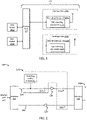
- FIG. 2 is a block diagram depicting an example of a remote antenna unit 104 with a TDD switching sub-system 110 according to one aspect.
- downlink signals received from the master unit 102 via an interface 202 can traverse a downlink path 204 and can be coupled to an antenna 209 via an interface 208 for transmission to communication devices in a coverage area.
- uplink signals received by the antenna 209 can be coupled to an uplink path 206 via the interface 208 and can traverse the uplink path 206 for transmission to the master unit 102 via the interface 202.
- the TDD switching sub-system 110 can include one or more components of the downlink path 204 and the uplink path 206.
- FIG. 2 depicts a TDD switching sub-system 110 that includes a switching control module 210, switches 212, 214 in the downlink path 204, and a switch 216 in the uplink path 206.
- the switching control module 210 can be coupled to the downlink path 204 in any suitable manner.
- the switch 212 can be positioned in the downlink path 204 between the interface 202 and a power amplifier 218.
- the switch 214 can be positioned in the downlink path 204 between the power amplifier 218 and the interface 208.
- the switch 216 can be positioned in the uplink path 206 between the interface 208 and a low noise amplifier 220.
- the switching control module 210 can control the operation of the switches 212, 214, 216 to selectively allow communication of downlink signals via the downlink path 204 or uplink signals via the uplink path 206.
- the switching control module 210 can control the switches 212, 214, 216 by sending switching signals to the switches 212, 214, 216 or devices actuating the switches 212, 214, 216 (not depicted in FIG. 2 ).
- the switching control module 210 can be communicatively coupled to the switches 212, 214, 216 or devices actuating the switches 212, 214, 216 via any suitable mechanism.
- the remote antenna unit 104 may include a printed circuit board or other communication bus via which switching signals from the switching control module 210 can provided to the switches 212, 214, 216 or devices actuating the switches 212, 214, 216.
- the switching control module 210 can provide switching signals that cause the switches 212, 214 to be closed and the switch 216 to be opened, thereby completing the downlink path 204 between the interfaces 202, 208 and opening the uplink path 206 between the interfaces 202, 208.
- the switching control module 210 can provide switching signals that cause the switches 212, 214 to be opened and the switch 216 to be closed, thereby opening the downlink path 204 between the interfaces 202, 208 and completing the uplink path 206 between the interfaces 202, 208.
- Any suitable switches 212, 214, 216 can be used.
- Non-limiting example of suitable switches 212, 214, 216 include RF switches, RF attenuators, digital attenuators in a digital signal path, digital switches interrupting a digital signal in a digital signal path, etc.
- FIG. 2 depicts the switching control module 210 as a separate module coupled to the downlink path 204 for illustrative purposes, other implementations are possible.
- the downlink path 204 may include one or more digital signal processing components, such as a processing device (e.g., an application-specific integrated circuit ("ASIC"), a field-programmable gate array (“FPGA”), etc.)
- ASIC application-specific integrated circuit
- FPGA field-programmable gate array
- the functions of the switching control module 210 can be performed by the processing device using digital downlink signals in the downlink path 204 between the interfaces 202, 208.
- the switching control module 210 can provide switching signals based on a detection of downlink signals in the downlink path 204, an internal clock, or a combination thereof.
- FIG. 3 is a block diagram depicting an example of the switching control module 210 according to one aspect.
- the switching control module 210 can detect the downlink/uplink ratio of the base stations 101a, 101b of other signals sources.
- the switching control module 210 can determine an initial clock setting for the TDD switching sub-system based on the downlink/uplink ratio.
- the initial clock setting can determine the timing of sending switching signals to the switches 212, 214, 216.
- the switching control module 210 can optimize switching times for the switches 212, 214, 216. Optimizing the switching times can maximize or otherwise improve data throughput via the DAS 100.
- the switching control module 210 can include a measurement receiver 302, a comparator 304, and a processor 306 communicatively coupled to a memory 308.
- the measurement receiver 302 can include any suitable device for measuring a signal power level in the downlink path 204.
- a non-limiting example of a measurement receiver 302 is a power detector.
- the measurement receiver 302 can be coupled to the downlink path 204 in any suitable manner, such as (but not limited to) a directional coupler.
- the comparator 304 can include a first input coupled to an output of the measurement receiver 302 and a second input coupled to a reference source 312.
- the measurement receiver 302 can provide a voltage or current representative of a signal power measurement for the downlink path 204 to the first input of the comparator 304.
- the reference source 312 can provide a voltage or current representative of a threshold signal power to the second input of the comparator 304.
- the comparator 304 can compare the representative voltages or currents for the downlink signal power measurement and the threshold signal power.
- the comparator 304 can output a voltage or current representative of whether the downlink signal power measurement exceeds the threshold signal power.
- the threshold signal power can be modified by modifying the voltage or current provided by the reference source 312.
- the processor 306 can receive the voltage or current representative of whether the downlink signal power measurement exceeds the threshold signal power.
- the processor 306 can control switching operations of the TDD switching sub-system 100 based on the comparison of the downlink signal power measurement and the threshold signal power by executing a switching control engine 310 or other executable instructions stored to the memory 308, as described in further detail below.
- the processor 306 can control the switching operations by generating switching signals that are provided to the switches 212, 214, 216 or the devices used for actuating the switches 212, 214, 216.
- the processor 306 can include any device or group of devices suitable for accessing and executing executable instructions stored in the memory 308.
- Non-limiting examples of the processor 306 include a microprocessor, an ASIC, a FPGA, or other suitable processing device.
- the processor 306 may include one processor or any number of processors.
- the memory 308 may be any non-transitory computer-readable medium capable of tangibly embodying executable instructions and can include electronic, magnetic, or optical devices. Examples of memory 308 include random access memory (“RAM”), read-only memory (“ROM”), magnetic disk, an ASIC, a configured processor, or other storage device. Instructions can be stored in memory 308 as executable code.
- the instructions can include processor-specific instructions generated by a compiler and/or an interpreter from code written in any suitable computer-programming language, such as C, C++, C#, Visual Basic, Java, Python, Perl, JavaScript, and ActionScript.
- FIG. 3 depicts a switching control module 210 including a comparator 304 for outputting a signal indicative of whether the downlink signal power exceeds a threshold signal power
- the comparator 304 and the reference source 312 can be omitted.
- the processor 306 can communicate with the measurement receiver 302 to obtain data describing signal power levels in the downlink path 204.
- the measurement receiver 302 can have an analog output electrically connected to the processor 306.
- the measurement receiver 302 can provide a voltage or a current to the processor 306 via the analog output. The voltage or current can be equivalent to or otherwise indicative of the measured power level in the downlink path 204.
- the measurement receiver 302 can provide a digital output signal to the processor 306 that represents the measured power level in the downlink path 204.
- the measurement receiver 302 can include a digital input that is coupled to the downlink path 304.
- the processor 306 can compare the data obtained from the measurement receiver 302 with data stored in the memory 308 that describes the threshold signal power.
- the threshold signal power can be modified by providing updated data describing the threshold signal power to the processor 306 for storage in the memory 308.
- FIG. 4 is a flow chart depicting an example of a process 400 for determining an initial clock setting for the switching control module 210 according to one aspect.
- the process 400 is described with respect to the implementation of the TDD switching sub-system 110 and the switching control module 210 described above with respect to FIGs. 2-3 . Other implementations, however, are possible.
- the process 400 is used to automatically determine a TDD configuration for one or more telecommunication operators using the DAS 100. Automatically determining the TDD configuration can reduce or eliminate the need for manual configuration of the DAS 100 with respect to each telecommunication operator. Reducing or eliminating the need for manual configuration of the DAS 100 can reduce or avoid problems resulting from missing information with respect to the configuration settings of different telecommunication operators.
- the process 400 involves obtaining multiple downlink frame samples by measuring signal power in a downlink path of a TDD DAS at multiple times, as depicted in block 410.
- the processor 306 can execute the switching control engine 310 to sample data from the measurement receiver 302 or the comparator 304 at intervals specified by the switching control engine 310. For each interval, the processor 306 stores data in the memory 308 describing whether the signal power in the downlink path 204 exceeds the threshold power. The signal power in the downlink path 204 exceeding the threshold power can indicate that a downlink frame is being transmitted via the downlink path 204.
- the signal power in the downlink path 204 being less than or equal to the threshold power can indicate that a downlink frame is not being transmitted via the downlink path 204 and that an uplink frame is being transmitted via the uplink path 206.
- the measurement receiver 302 can measure the signal power in the downlink path 204 at intervals specified by the processor 306. In other aspects, the measurement receiver 302 can continuously measure the signal power in the downlink path 204.
- the processor 306 can sample power measurements from measurement receiver 302 or sample current or voltage levels at the output of the comparator 304 at the specified intervals.
- the process 400 further involves determining a downlink/uplink ratio for the TDD DAS based on the downlink frame samples, as depicted in block 420.
- the switching control engine 310 accesses data describing different downlink/uplink ratios for different TDD configurations. Different TDD configurations communicate TDD signals in a specified ratio between the uplink and downlink sub-frames.
- a frame can be a period of time a TDD system switches between sending uplink and downlink data in according to a specified sequence.
- a frame can include uplink sub-frames during which uplink data is transmitted and downlink sub-frames during which uplink data is transmitted.
- the downlink/uplink ratio can include the number of individual downlink and uplink subframes and the duration of each sub-frame.
- the process 400 further involves determining an initial clock setting for the switching control module 210 based on the downlink/uplink ratio, as depicted in block 430.
- the processor 306 can execute the switching control engine 310 to determine the initial clock setting.
- the clock setting can be used to determine when the processor 306 provides a switching signal to the switches 212, 214, 216.
- the processor 306 can provide the switching signal every t clk seconds, milliseconds, microseconds, or other suitable unit of time.
- the value of t clk used for the clock setting can correspond to the TDD configuration of a telecommunication operator using the DAS 100.
- An initial value of t clk can be selected based on a TDD configuration determined from the downlink/uplink ratio.
- a TDD configuration of a base station using the DAS 100 can be determined by identifying downlink sub-frames and uplink sub-frames during a TDD frame can be used to determine.
- a downlink/uplink ratio can correspond to a given TDD configuration.
- an LTE system configured for TDD operation can include a first configuration with a ratio of two downlink sub-frames to three uplink sub-frames, a second configuration with a ratio of three downlink sub-frames to two uplink sub-frames, a third configuration with a ratio of four downlink sub-frames to one uplink sub-frames, etc.
- the switching control engine 310 can select a TDD configuration based on a standardized downlink/uplink ratio in a telecommunication standard, such as a 3rd Generation Partnership Project ("3GPP") specification. Selecting the TDD configuration based on a standardized downlink/uplink ratio in a telecommunication standard can minimize or otherwise reduce errors with respect to incorrect switching intervals.
- the switching control engine 310 can be configured via user input with one or more specified TDD configurations corresponding to one or more specified downlink/uplink ratios.
- the switching control engine 310 can compare the downlink/uplink ratio determined using the measurement receiver 302 to data stored to the memory device that describes various TDD configurations.
- the switching control engine 310 can identify the TDD configuration for an operator using the DAS 100 based on the comparison of the determined downlink/uplink ratio with the stored data describing various TDD configurations.
- the switching control engine 310 can select an initial value for t clk that causes the processor 306 to send switching signals to the switches 212, 214, 216 in accordance with the identified TDD configuration.
- the DAS 100 can be set to an offline mode for performing the process 400.
- the DAS 100 may be automatically set to an initialization mode upon entering operation.
- An initialization or other offline mode can be used to set one or more system parameters of the DAS 100 used for TDD operation.
- the switching control module 210 may perform one or more configuration operations based on signal power measurements in the downlink path 204 without controlling the switches 212, 214, 216.
- the switches 212, 214, 216 may be set to an open position such the DAS 100 does not communicate signals between the base stations 101a, 101b and the coverage areas 108a, 108b.
- the initial clock setting t clk may roughly approximate the TDD configuration for an operator using the DAS 100. However, slight discrepancies may exist between the times at which downlink sub-frames begin and the times at which the switching control module 210 provides switching signals to the switches 212, 214, 216.
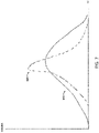
- FIG. 5 is a graph depicting examples of switching time differentials ⁇ t 1... n between downlink sub-frames 502a-n and switching signals 504a-n provided according to an initial clock setting according to one aspect.
- Each of the switching time differentials ⁇ t 1... n is a delay between the start of a respective one of the downlink sub-frames 502a-n and a time at which a respective one of the switching signals 504a-n is provided to the switches 212, 214,216.
- the switching control module 210 can optimize or otherwise improve the clock setting t clk based on a switching time adjustment ⁇ t adj statistically determined from a set of switching time differentials ⁇ t n .
- the processor 306 can compare each of the clock settings t clk ,1... n with a respective one of the times t DL ,1... n at which a downlink signal power greater than a threshold signal power is detected by the switching control module 210.
- the offset value t offset can be a configurable static offset between the switching point determined by the measurement receiver 302 and the point in time when the switching point is required to be set.
- the switching control module 210 can be configured to detect a threshold signal power that is substantially higher than the noise in the downlink path 204, thereby maintaining a high signal-to-noise ratio and a low statistical variance.
- the offset value t offset can be used if it is desirable to switch between the uplink and downlink mode prior to the signal power in the downlink path 204 exceeding the high threshold signal power.
- the offset value t offset can be selected based on the threshold signal power used by the switching control module 210, the telecommunication standard used for downlink signals in the downlink signal path 204, the use of the DAS 100 by multiple operators, or the transmission of multi-channel signals via the DAS 100.
- the switching time differential ⁇ t n can be determined without using an offset value t offset .
- the statistical variation of a determined switching point over time can be caused by one or more processes in combination with one another.
- a source of the variation is the signal-to-noise level of the signal measured by the measurement receiver 302.
- Another non-limiting example of a source of variation is the jitter and drift of a reference clock used by the switching engine 310 or other clocks in DAS 100 or the base stations 101a, 101b.
- Another non-limiting example of a source of variation is noise in the associated with the reference source 312.
- Another non-limiting example of a source of variation is that high power uplink signals can be coupled to the downlink path 204 due to missing isolation between the uplink and downlink paths at the master unit 102.
- the various source of variation can combine with one another to cause a statistical variation in the switching point.
- FIG. 6 is a graph depicting an example of a statistical distribution of switching time differentials ⁇ t n used to find a switching time adjustment ⁇ t adj .
- Sampled values for ⁇ t n can be obtained over different frames in which an operator using the DAS 100 switches between an uplink mode and a downlink mode.
- the switching control engine 310 can generate or otherwise obtain a statistical distribution of the sampled values for ⁇ t n .
- the switching control engine 310 can determine the switching time adjustment ⁇ t adj based on the statistical distribution.
- a non-limiting example of a switching time adjustment ⁇ t adj statistically determined from sampled values for ⁇ t n is a mean value ⁇ t mean of the sampled values for ⁇ t n , as depicted in FIG. 6 .
- the signal-to-noise level in the downlink path 204 can impact the statistical distribution of the sampled values of ⁇ t n .
- FIG. 7 is a graph depicting examples of statistical distributions of switching time differentials ⁇ t n affected by a signal-to-noise level in the downlink path 204.
- a statistical distribution 602 of switching time differentials ⁇ t n represented by the solid line may obtained from a downlink path 204 having a lower signal-to-noise ratio than the statistical distribution 604 represented by the dashed line.
- the lower signal-to-noise ratio can cause the statistical distribution 602 of switching time differentials ⁇ t n to have a wider range of values than the statistical distribution 604.
- FIGs. 6-7 depict symmetrical or nearly symmetrical statistical distributions of the sampled values of ⁇ t n .
- the statistical distribution of the sampled values of ⁇ t n may be asymmetrical.
- the statistical distribution may be wider for earlier times and narrow for later times due to the higher signal level.
- the switching control module 210 can use a switching time adjustment ⁇ t adj to optimize or otherwise improve the clock setting used by the switching control module 210.
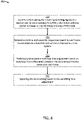
- FIG. 8 is a flow chart depicting an example of a process for determining an optimized clock setting for the switching control module according to one aspect.
- the process 700 involves identifying a clock setting that controls timing for providing switching signals to one or more switches that instruct the switches to switch the distributed antenna system between an uplink mode and a downlink mode, as depicted in block 710.
- the switching control engine 310 executed by the processor 306 can determine a clock setting for providing switching signals to one or more of the switches 212,214,216.
- identifying the clock setting can include identifying an initial clock setting for the switching control module 210, such as (but not limited to) a clock setting determined using a process 400.
- the clock setting can be determined or otherwise identified during an offline mode for the DAS 100 in which no switching signals are provided to the switches 212, 214, 216.
- the identified clock setting can be a current clock setting for a DAS 100 in an online mode in which signals are communicated with coverage areas 108a, 108b.
- the current clock setting can be the clock setting used for providing switching signals to the switches 212, 214, 216 in the online mode of the DAS 100.
- the switching control engine 310 can identify the current clock setting and perform additional operations to optimize or otherwise update the current clock setting.
- the process 700 further involves determining start or end times for respective downlink sub-frames transmitted via a downlink path of the distributed antenna system, as depicted in block 720.
- the switching control engine 310 can receive or otherwise access data describing power measurements by the measurement receiver 302.
- the switching control engine 310 can identify a start time for a respective downlink sub-frame based on a power measurement indicating that a signal power in the downlink path 204 exceeds the threshold signal power.
- the switching control engine 310 can identify an end time for a respective downlink sub-frame based on a power measurement indicating that a signal power in the downlink path 204 drops from a level exceeding the threshold signal power to a level below the threshold signal power.
- the process 700 further involves statistically determining a switching time adjustment based on switching time differentials between the clock setting and the respective start times, as depicted in block 730.
- the switching control engine 310 can determine a switching time adjustment that is a mean or other statistical attribute of a set of sample switching time differentials, as described above with respect to FIGs. 5-6 .
- the process 700 further involves updating the clock setting based on the switching time adjustment, as depicted in block 740.
- the switching control engine 310 can detect an end of a current TDD frame or sub-frame based on power measurements from the measurement receiver 302.
- the switching control engine 310 can generate switching signals for the switches 212, 214, 216 at intervals of t clk,updated after detecting the end of the current TDD frame or sub-frame.
- the TDD switching sub-system can be implemented in any suitable DAS 100 configured for TDD operations.
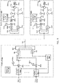
- FIG. 9 is a schematic depicting examples of a master unit 102 and remote antenna units 104a-n for an optical TDD distributed antenna system that can utilize an optimized clock setting for a TDD switching sub-system according to one aspect.
- the master unit 102 can include splitter-combiners 802a-n for isolating uplink and downlink signals communicated with base stations or other signal sources.
- the master unit 102 can also include mixers 803a-n and local oscillators 804a-n for frequencyshifting downlink signals to intermediate frequency ("IF") bands, as described in greater detail below.
- the master unit 102 can also include a combiner 806 for combining downlink signals from different operators for serial transmission to remote antenna units 104a-n.
- the master unit 102 can also include an electrical-to-optical converter 808 for converting the serialized electrical downlink signals into serialized optical downlink signals.
- the serialized optical downlink signals can be transmitted to the remote antenna units 104a-n via the optical communication link 811.
- the master unit 102 can also include an optical-to-electrical converter 812 for converting optical uplink signals received via the optical communication link 811 into serialized electrical uplink signals.
- the master unit 102 can also include a splitter 814 for separating the serialized electrical uplink signals into separate uplink signals for transmission to base stations or other receivers of uplink signals.
- the remote antenna units 104a-n can include respective optical splitter-combiners 816a-n for isolating optical downlink signals from optical uplink signals.
- the remote antenna units 104a-n can also include respective optical-to-electrical converters 818a-n for converting optical downlink signals into electrical downlink signals.
- the remote antenna units 104a-n can also include respective mixers 820a-n and local oscillators 821an for frequency shifting downlink signals to RF frequency bands, as described in detail below.
- the remote antenna units 104a-n can also include respective bandpass filters 822an for attenuating unwanted frequency components of the RF downlink signals outputted by the mixers 820a-n.
- the remote antenna units 104a-n can also include switching control modules 210a-n and switches 212a-n, 214a-n, 216a-n that perform the same or similar functions with respect to the power amplifiers 218a-n and low noise amplifiers 220a-n as described above with respect to FIG. 2 .
- the remote antenna units 104a-n can also include respective circulators 824a-n for coupling downlink signals from the downlink paths to the antennas 209a-n and for coupling uplink signals from the antennas 209a-n to the uplink paths.
- the remote antenna units 104a-n can also include respective electrical-to-optical converters 828a-for converting electrical uplink signals to optical uplink signals for transmission via the optical communication link 811.
- the DAS 100 can use a common optical communication link 811 between the master unit 102 and the remote antenna units 104a-n.
- the DAS 100 can support an "uncoordinated operator mode." In the uncoordinated operator mode, different operators using the DAS 100 do not coordinate with one another in switching between an uplink TDD mode and a downlink TDD mode.
- the DAS 100 can be configured to reduce or eliminate uplink blocking by unsynchronized operators transmitting signals using adjacent frequencies. For example, downlink signals from multiple operators can be closely spaced within a frequency band (e.g., a few MHz).
- the mixers 803a-n and the local oscillators 804a-n of the master unit 102 can be used to frequency-shift downlink signals to IF bands. Frequency shifting the downlink signals to IF bands can separate downlink signals from uncoordinated operators use closely spaced frequencies for transmitting TDD signals.
- the mixers 820a-n and local oscillators 821a-n of the remote antenna units 104a-n can be used to frequency-shift the IF downlink signals back to RF bands for transmission.
- a reference clock 805 in the master unit 102 can be used for synchronizing the local oscillators 804a-n, 821a-n. In some aspects, the reference clock 805 can also be used for synchronizing the reference source 312 used by the switching control module 210.
- the reference clock 805 can be communicatively coupled to the local oscillators 804a-n via any suitable mechanism, such as a printed circuit board or other communication bus (not depicted in FIG. 9 ). Signals from the reference clock 805 can be communicated from the master unit 102 to the remote antenna units 104a-n via the optical communication link 811.
Description
- The present disclosure relates generally to telecommunication systems and more particularly (although not necessarily exclusively) to switching sub-systems for distributed antenna systems using time division duplexing.
- Telecommunications operators use telecommunication systems to provide signal coverage to coverage zones in which wireless devices are located. A distributed system ("DAS") may be used to extend the coverage of such telecommunication systems. Such distributed antenna systems include signal paths between base stations or other signal sources operated by telecommunication operators and remote antenna units positioned in one or more geographical coverage areas.
- In some implementations, a DAS may be configured for time division duplexing ("TDD") operations in which downlink and uplink signals are respectively transmitted and received using at least some common frequencies or common portions of a signal path. A DAS configured for TDD operations may include one or more switches for isolating downlink signal paths from uplink signal paths.
- In some cases, multiple telecommunication operators may use the same DAS for extending the coverage of their respective telecommunication systems. An entity responsible for configuring or otherwise operating the DAS may be independent of the telecommunication operators that use the DAS. The entity being independent of the telecommunication operators may present disadvantages. For example, it may be difficult or infeasible to configure the switching operations of the DAS in accordance with the TDD configuration used by the telecommunication operators.
- Systems and methods for optimizing TDD switching operations for a DAS are desirable.
-
US 2009/316611 A1 discloses a method of determining a boundary of a subframe in a time division duplexing (TDD) system. In the method, a power level of a signal on at least one radio frequency is detected, the signal comprising at least one subframe. A time domain correlation is done on the detected signal with a first reference signal, wherein the first reference signal represents at least one subframe. The location and time of a boundary of the at least one subframe of the detected signal is determined based on the correlation of the detected signal and the first reference signal. - The invention is defined by the appended claims.
- These illustrative aspects and features are mentioned not to limit or define the disclosure, but to provide examples to aid understanding of the concepts disclosed in this application. Other aspects, advantages, and features of the present disclosure will become apparent after review of the entire application.
-
-
FIG. 1 is a block diagram depicting an example of a distributed antenna system having a time-division duplex ("TDD") switching sub-system according to one aspect of the present disclosure. -
FIG. 2 is a block diagram depicting an example of a remote antenna unit with a TDD switching sub-system according to one aspect of the present disclosure. -
FIG. 3 is a block diagram depicting an example of a switching control module of the TDD switching sub-system ofFIG. 2 according to one aspect of the present disclosure. -
FIG. 4 is a flow chart depicting an example of a process for determining an initial clock setting for the switching control module according to one aspect of the present disclosure. -
FIG. 5 is a graph depicting examples of switching time differentials between downlink sub-frames and switching signals provided according to an initial clock setting according to one aspect of the present disclosure. -
FIG. 6 is a graph depicting an example of a statistical distribution of switching time differentials used to find a switching time adjustment according to one aspect of the present disclosure. -
FIG. 7 is a graph depicting examples of statistical distributions of switching time differentials affected by a signal-to-noise level in the downlink path according to one aspect of the present disclosure. -
FIG. 8 is a flow chart depicting an example of a process for determining an optimized clock setting for the switching control module according to one aspect of the present disclosure. -
FIG. 9 is a schematic depicting examples of a master unit and remote antenna units for an optical TDD distributed antenna system that can utilize an optimized clock setting for a TDD switching sub-system according to one aspect of the present disclosure. - Certain aspects and examples are directed to switching sub-systems for a distributed antenna system ("DAS") configured for time division duplexing ("TDD") operations. For example, the DAS can use a switching sub-system to switch between an uplink mode for communicating TDD signals in an uplink direction and a downlink mode for communicating TDD signals in a downlink direction. The switching sub-system can automatically determine switching times for the DAS based on determining whether a signal level for downlink signals exceeds a threshold level. One or more switches of the switching sub-system can switch a remote antenna unit of the DAS to the downlink mode by selectively connecting one or more components of the downlink path in the remote antenna unit and disconnecting one or more components of a corresponding uplink path in the remote antenna unit.
- In accordance with some aspects, the switching sub-system can include a switching control module that detects the downlink/uplink ratio of base stations in communication with the DAS. The switching control module can determine an initial clock setting based on the downlink/uplink ratio. The initial clock setting can determine the timing for sending command signals to the switches of the switching sub-system that instruct the switches to switch the DAS between an uplink mode and a downlink mode.
- The switching control module can also optimize a clock setting that controls switching times for the switches. Optimizing the switching times can maximize or otherwise improve data throughput via the DAS. The switching control module can optimize the clock setting by determining start or end times for respective downlink subframes transmitted via the downlink path. The switching control module can determine the start or end times based on when signal power measurements for the downlink path exceed a threshold signal power. The switching control module can statistically determine a switching time adjustment based on a set of switching time differentials between the initial clock setting and the determined start or end times for the downlink sub-frames. For example, the switching time adjustment may be the statistical mean of the set of switching time differentials. The switching control module can update the clock setting based on the switching time adjustment.
- The switching control module can be used to automatically determine a TDD configuration for one or more telecommunication operators using the DAS. Automatically determining the TDD configuration can reduce or eliminate the need for manual configuration of the DAS with respect to each telecommunication operator. Reducing or eliminating the need for manual configuration of the DAS can reduce or avoid problems resulting from missing information with respect to the configuration settings of different telecommunication operators. The switching control module can also compensate for uplink or downlink pulsing variation or other deficiencies components of the DAS in the uplink or downlink direction, such as a jitter or clock frequency drift experienced by one or more reference clock devices in the DAS.
- Detailed descriptions of certain examples are discussed below. These illustrative examples are given to introduce the reader to the general subject matter discussed here and are not intended to limit the scope of the disclosed concepts. The following sections describe various additional aspects and examples with reference to the drawings in which like numerals indicate like elements, and directional descriptions are used to describe the illustrative examples but, like the illustrative examples, should not be used to limit the present disclosure.
-
FIG. 1 is a block diagram depicting an example ofDAS 100 having aTDD switching sub-system 110 according to one aspect. The DAS 100 can include amaster unit 102 in communication withremote antenna units base stations 101a, 101b. In some aspects, different base stations can communicate signals associated with different telecommunication operators. The DAS 100 can be positioned in a geographical area (e.g., a stadium, an office building, etc.) to extend wireless communication coverage of thebase stations 101a, 101b intogeographical coverage areas - The
DAS 100 or other telecommunication system can include downlink paths for transporting downlink signals from thebase stations 101a, 101b to one or more of theremote antenna units base stations 101a, 101b via a wired or wireless communication medium. Downlink signals can include signals provided from thebase stations 101a, 101b and transmitted by theremote antenna units coverage areas - The
DAS 100 or other telecommunication system can also include uplink paths for transporting uplink signals from one or more of theremote antenna units remote antenna units coverage areas - The
master unit 102 can communicate signals between thebase stations 101a, 101b and theremote antenna units master unit 102 is a wireless conversion station. Themaster unit 102 and remote antenna unit(s) 104a, 104b can communicate via any suitable communication medium. The communication medium can be any suitable medium for providing a serial communication link between themaster unit 102 and theremote antenna unit master unit 102 andremote antenna units - For illustrative purposes,
FIG. 1 depicts asingle master unit 102 in communication with twobase stations 101a, 101b and tworemote antenna units antenna system 100 can include any number of master units and any number of remote antenna units for communicating signals between any number of base stations or other signal sources and any number of coverage areas. - A
DAS 100 can include other devices in addition to master units, remote antenna units, and extension units. For example, in some aspects, theDAS 100 may include a base station router or other interface device that receives signals frombase stations 101a, 101b and provides the signals to themaster unit 102. In other aspects, theDAS 100 may include one or more extension units that communicate signals between themaster unit 102 and theremote antenna units - The
DAS 100 can be configured for TDD operations that support multiple operators communicating signals via theDAS 100. For example, theDAS 100 can switch between an uplink mode for communicating TDD signals in an uplink direction and a downlink mode for communicating TDD signals in a downlink direction. - The
remote antenna units TDD switching sub-systems 110a, 110b used to connect components of the downlink path in response to detecting downlink signals having signal levels exceeding a threshold level. TheTDD switching sub-systems 110a, 110b can analyze downlink signals to determine if signal levels for the downlink signals exceed specified threshold levels. Each of theTDD switching sub-systems 110a, 110b can include switches that switch a respective one of theremote antenna units -
FIG. 2 is a block diagram depicting an example of aremote antenna unit 104 with aTDD switching sub-system 110 according to one aspect. In a downlink direction, downlink signals received from themaster unit 102 via aninterface 202 can traverse adownlink path 204 and can be coupled to anantenna 209 via aninterface 208 for transmission to communication devices in a coverage area. In an uplink direction, uplink signals received by theantenna 209 can be coupled to anuplink path 206 via theinterface 208 and can traverse theuplink path 206 for transmission to themaster unit 102 via theinterface 202. - The
TDD switching sub-system 110 can include one or more components of thedownlink path 204 and theuplink path 206. For example,FIG. 2 depicts aTDD switching sub-system 110 that includes a switchingcontrol module 210, switches 212, 214 in thedownlink path 204, and aswitch 216 in theuplink path 206. The switchingcontrol module 210 can be coupled to thedownlink path 204 in any suitable manner. Theswitch 212 can be positioned in thedownlink path 204 between theinterface 202 and apower amplifier 218. Theswitch 214 can be positioned in thedownlink path 204 between thepower amplifier 218 and theinterface 208. Theswitch 216 can be positioned in theuplink path 206 between theinterface 208 and alow noise amplifier 220. - The switching
control module 210 can control the operation of theswitches downlink path 204 or uplink signals via theuplink path 206. The switchingcontrol module 210 can control theswitches switches switches FIG. 2 ). The switchingcontrol module 210 can be communicatively coupled to theswitches switches remote antenna unit 104 may include a printed circuit board or other communication bus via which switching signals from the switchingcontrol module 210 can provided to theswitches switches control module 210 can provide switching signals that cause theswitches switch 216 to be opened, thereby completing thedownlink path 204 between theinterfaces uplink path 206 between theinterfaces control module 210 can provide switching signals that cause theswitches switch 216 to be closed, thereby opening thedownlink path 204 between theinterfaces uplink path 206 between theinterfaces suitable switches suitable switches - Although
FIG. 2 depicts the switchingcontrol module 210 as a separate module coupled to thedownlink path 204 for illustrative purposes, other implementations are possible. In some aspects, thedownlink path 204 may include one or more digital signal processing components, such as a processing device (e.g., an application-specific integrated circuit ("ASIC"), a field-programmable gate array ("FPGA"), etc.) The functions of the switchingcontrol module 210 can be performed by the processing device using digital downlink signals in thedownlink path 204 between theinterfaces - The switching
control module 210 can provide switching signals based on a detection of downlink signals in thedownlink path 204, an internal clock, or a combination thereof. For example,FIG. 3 is a block diagram depicting an example of the switchingcontrol module 210 according to one aspect. The switchingcontrol module 210 can detect the downlink/uplink ratio of thebase stations 101a, 101b of other signals sources. The switchingcontrol module 210 can determine an initial clock setting for the TDD switching sub-system based on the downlink/uplink ratio. The initial clock setting can determine the timing of sending switching signals to theswitches control module 210 can optimize switching times for theswitches DAS 100. - The switching
control module 210 can include ameasurement receiver 302, acomparator 304, and aprocessor 306 communicatively coupled to amemory 308. - The
measurement receiver 302 can include any suitable device for measuring a signal power level in thedownlink path 204. A non-limiting example of ameasurement receiver 302 is a power detector. Themeasurement receiver 302 can be coupled to thedownlink path 204 in any suitable manner, such as (but not limited to) a directional coupler. - The
comparator 304 can include a first input coupled to an output of themeasurement receiver 302 and a second input coupled to areference source 312. Themeasurement receiver 302 can provide a voltage or current representative of a signal power measurement for thedownlink path 204 to the first input of thecomparator 304. Thereference source 312 can provide a voltage or current representative of a threshold signal power to the second input of thecomparator 304. Thecomparator 304 can compare the representative voltages or currents for the downlink signal power measurement and the threshold signal power. Thecomparator 304 can output a voltage or current representative of whether the downlink signal power measurement exceeds the threshold signal power. The threshold signal power can be modified by modifying the voltage or current provided by thereference source 312. - The
processor 306 can receive the voltage or current representative of whether the downlink signal power measurement exceeds the threshold signal power. Theprocessor 306 can control switching operations of theTDD switching sub-system 100 based on the comparison of the downlink signal power measurement and the threshold signal power by executing a switching control engine 310 or other executable instructions stored to thememory 308, as described in further detail below. Theprocessor 306 can control the switching operations by generating switching signals that are provided to theswitches switches - The
processor 306 can include any device or group of devices suitable for accessing and executing executable instructions stored in thememory 308. Non-limiting examples of theprocessor 306 include a microprocessor, an ASIC, a FPGA, or other suitable processing device. Theprocessor 306 may include one processor or any number of processors. Thememory 308 may be any non-transitory computer-readable medium capable of tangibly embodying executable instructions and can include electronic, magnetic, or optical devices. Examples ofmemory 308 include random access memory ("RAM"), read-only memory ("ROM"), magnetic disk, an ASIC, a configured processor, or other storage device. Instructions can be stored inmemory 308 as executable code. The instructions can include processor-specific instructions generated by a compiler and/or an interpreter from code written in any suitable computer-programming language, such as C, C++, C#, Visual Basic, Java, Python, Perl, JavaScript, and ActionScript. - Although
FIG. 3 depicts a switchingcontrol module 210 including acomparator 304 for outputting a signal indicative of whether the downlink signal power exceeds a threshold signal power, other implementations are possible. For example, in some aspects, thecomparator 304 and thereference source 312 can be omitted. Theprocessor 306 can communicate with themeasurement receiver 302 to obtain data describing signal power levels in thedownlink path 204. In one non-limiting example themeasurement receiver 302 can have an analog output electrically connected to theprocessor 306. Themeasurement receiver 302 can provide a voltage or a current to theprocessor 306 via the analog output. The voltage or current can be equivalent to or otherwise indicative of the measured power level in thedownlink path 204. In another non-limiting example, themeasurement receiver 302 can provide a digital output signal to theprocessor 306 that represents the measured power level in thedownlink path 204. In additional or alternative aspects, themeasurement receiver 302 can include a digital input that is coupled to thedownlink path 304. - The
processor 306 can compare the data obtained from themeasurement receiver 302 with data stored in thememory 308 that describes the threshold signal power. The threshold signal power can be modified by providing updated data describing the threshold signal power to theprocessor 306 for storage in thememory 308. -
FIG. 4 is a flow chart depicting an example of aprocess 400 for determining an initial clock setting for the switchingcontrol module 210 according to one aspect. For illustrative purposes, theprocess 400 is described with respect to the implementation of theTDD switching sub-system 110 and the switchingcontrol module 210 described above with respect toFIGs. 2-3 . Other implementations, however, are possible. - The
process 400 is used to automatically determine a TDD configuration for one or more telecommunication operators using theDAS 100. Automatically determining the TDD configuration can reduce or eliminate the need for manual configuration of theDAS 100 with respect to each telecommunication operator. Reducing or eliminating the need for manual configuration of theDAS 100 can reduce or avoid problems resulting from missing information with respect to the configuration settings of different telecommunication operators. - The
process 400 involves obtaining multiple downlink frame samples by measuring signal power in a downlink path of a TDD DAS at multiple times, as depicted inblock 410. For example, theprocessor 306 can execute the switching control engine 310 to sample data from themeasurement receiver 302 or thecomparator 304 at intervals specified by the switching control engine 310. For each interval, theprocessor 306 stores data in thememory 308 describing whether the signal power in thedownlink path 204 exceeds the threshold power. The signal power in thedownlink path 204 exceeding the threshold power can indicate that a downlink frame is being transmitted via thedownlink path 204. The signal power in thedownlink path 204 being less than or equal to the threshold power can indicate that a downlink frame is not being transmitted via thedownlink path 204 and that an uplink frame is being transmitted via theuplink path 206. In some aspects, themeasurement receiver 302 can measure the signal power in thedownlink path 204 at intervals specified by theprocessor 306. In other aspects, themeasurement receiver 302 can continuously measure the signal power in thedownlink path 204. Theprocessor 306 can sample power measurements frommeasurement receiver 302 or sample current or voltage levels at the output of thecomparator 304 at the specified intervals. - The
process 400 further involves determining a downlink/uplink ratio for the TDD DAS based on the downlink frame samples, as depicted inblock 420. For example, the switching control engine 310 accesses data describing different downlink/uplink ratios for different TDD configurations. Different TDD configurations communicate TDD signals in a specified ratio between the uplink and downlink sub-frames. A frame can be a period of time a TDD system switches between sending uplink and downlink data in according to a specified sequence. A frame can include uplink sub-frames during which uplink data is transmitted and downlink sub-frames during which uplink data is transmitted. The downlink/uplink ratio can include the number of individual downlink and uplink subframes and the duration of each sub-frame. - The
process 400 further involves determining an initial clock setting for the switchingcontrol module 210 based on the downlink/uplink ratio, as depicted inblock 430. For example, theprocessor 306 can execute the switching control engine 310 to determine the initial clock setting. The clock setting can be used to determine when theprocessor 306 provides a switching signal to theswitches processor 306 can provide the switching signal every tclk seconds, milliseconds, microseconds, or other suitable unit of time. The value of tclk used for the clock setting can correspond to the TDD configuration of a telecommunication operator using theDAS 100. An initial value of tclk can be selected based on a TDD configuration determined from the downlink/uplink ratio. - A TDD configuration of a base station using the
DAS 100 can be determined by identifying downlink sub-frames and uplink sub-frames during a TDD frame can be used to determine. A downlink/uplink ratio can correspond to a given TDD configuration. For example, an LTE system configured for TDD operation can include a first configuration with a ratio of two downlink sub-frames to three uplink sub-frames, a second configuration with a ratio of three downlink sub-frames to two uplink sub-frames, a third configuration with a ratio of four downlink sub-frames to one uplink sub-frames, etc. In some aspects, the switching control engine 310 can select a TDD configuration based on a standardized downlink/uplink ratio in a telecommunication standard, such as a 3rd Generation Partnership Project ("3GPP") specification. Selecting the TDD configuration based on a standardized downlink/uplink ratio in a telecommunication standard can minimize or otherwise reduce errors with respect to incorrect switching intervals. In other aspects, the switching control engine 310 can be configured via user input with one or more specified TDD configurations corresponding to one or more specified downlink/uplink ratios. - The switching control engine 310 can compare the downlink/uplink ratio determined using the
measurement receiver 302 to data stored to the memory device that describes various TDD configurations. The switching control engine 310 can identify the TDD configuration for an operator using theDAS 100 based on the comparison of the determined downlink/uplink ratio with the stored data describing various TDD configurations. The switching control engine 310 can select an initial value for tclk that causes theprocessor 306 to send switching signals to theswitches - In some aspects, the
DAS 100 can be set to an offline mode for performing theprocess 400. For example, theDAS 100 may be automatically set to an initialization mode upon entering operation. An initialization or other offline mode can be used to set one or more system parameters of theDAS 100 used for TDD operation. In an offline mode, the switchingcontrol module 210 may perform one or more configuration operations based on signal power measurements in thedownlink path 204 without controlling theswitches switches DAS 100 does not communicate signals between thebase stations 101a, 101b and thecoverage areas - The initial clock setting tclk may roughly approximate the TDD configuration for an operator using the
DAS 100. However, slight discrepancies may exist between the times at which downlink sub-frames begin and the times at which theswitching control module 210 provides switching signals to theswitches FIG. 5 is a graph depicting examples of switching time differentials Δt 1...n betweendownlink sub-frames 502a-n and switchingsignals 504a-n provided according to an initial clock setting according to one aspect. Each of the switching time differentials Δt 1...n is a delay between the start of a respective one of thedownlink sub-frames 502a-n and a time at which a respective one of the switching signals 504a-n is provided to theswitches 212, 214,216. - The switching
control module 210 can optimize or otherwise improve the clock setting tclk based on a switching time adjustment Δtadj statistically determined from a set of switching time differentials Δtn . For example, for one or more of thedownlink sub-frames 502a-n, theprocessor 306 can compare each of the clock settings t clk,1...n with a respective one of the times t DL,1...n at which a downlink signal power greater than a threshold signal power is detected by the switchingcontrol module 210. - The processor can determine each switching time differential Δtn = |tclk,n - tDL,n - toffset |. The offset value toffset can be a configurable static offset between the switching point determined by the
measurement receiver 302 and the point in time when the switching point is required to be set. The switchingcontrol module 210 can be configured to detect a threshold signal power that is substantially higher than the noise in thedownlink path 204, thereby maintaining a high signal-to-noise ratio and a low statistical variance. The offset value toffset can be used if it is desirable to switch between the uplink and downlink mode prior to the signal power in thedownlink path 204 exceeding the high threshold signal power. The offset value toffset can be selected based on the threshold signal power used by the switchingcontrol module 210, the telecommunication standard used for downlink signals in thedownlink signal path 204, the use of theDAS 100 by multiple operators, or the transmission of multi-channel signals via theDAS 100. In some aspects, the switching time differential Δtn can be determined without using an offset value toffset. - The statistical variation of a determined switching point over time can be caused by one or more processes in combination with one another. One non-limiting example of a source of the variation is the signal-to-noise level of the signal measured by the
measurement receiver 302. Another non-limiting example of a source of variation is the jitter and drift of a reference clock used by the switching engine 310 or other clocks inDAS 100 or thebase stations 101a, 101b. Another non-limiting example of a source of variation is noise in the associated with thereference source 312. Another non-limiting example of a source of variation is that high power uplink signals can be coupled to thedownlink path 204 due to missing isolation between the uplink and downlink paths at themaster unit 102. The various source of variation can combine with one another to cause a statistical variation in the switching point. -
FIG. 6 is a graph depicting an example of a statistical distribution of switching time differentials Δtn used to find a switching time adjustment Δtadj . Sampled values for Δtn can be obtained over different frames in which an operator using theDAS 100 switches between an uplink mode and a downlink mode. The switching control engine 310 can generate or otherwise obtain a statistical distribution of the sampled values for Δtn . The switching control engine 310 can determine the switching time adjustment Δtadj based on the statistical distribution. A non-limiting example of a switching time adjustment Δtadj statistically determined from sampled values for Δtn is a mean value Δtmean of the sampled values for Δtn , as depicted inFIG. 6 . - The signal-to-noise level in the
downlink path 204 can impact the statistical distribution of the sampled values of Δtn . For example,FIG. 7 is a graph depicting examples of statistical distributions of switching time differentials Δtn affected by a signal-to-noise level in thedownlink path 204. Astatistical distribution 602 of switching time differentials Δtn represented by the solid line may obtained from adownlink path 204 having a lower signal-to-noise ratio than thestatistical distribution 604 represented by the dashed line. The lower signal-to-noise ratio can cause thestatistical distribution 602 of switching time differentials Δtn to have a wider range of values than thestatistical distribution 604. -
FIGs. 6-7 depict symmetrical or nearly symmetrical statistical distributions of the sampled values of Δtn . However, in some aspects, the statistical distribution of the sampled values of Δtn may be asymmetrical. For example, the statistical distribution may be wider for earlier times and narrow for later times due to the higher signal level. - The switching
control module 210 can use a switching time adjustment Δtadj to optimize or otherwise improve the clock setting used by the switchingcontrol module 210.FIG. 8 is a flow chart depicting an example of a process for determining an optimized clock setting for the switching control module according to one aspect. - The
process 700 involves identifying a clock setting that controls timing for providing switching signals to one or more switches that instruct the switches to switch the distributed antenna system between an uplink mode and a downlink mode, as depicted inblock 710. For example, the switching control engine 310 executed by theprocessor 306 can determine a clock setting for providing switching signals to one or more of the switches 212,214,216. - In some aspects, identifying the clock setting can include identifying an initial clock setting for the switching
control module 210, such as (but not limited to) a clock setting determined using aprocess 400. For example, the clock setting can be determined or otherwise identified during an offline mode for theDAS 100 in which no switching signals are provided to theswitches - In other aspects, the identified clock setting can be a current clock setting for a
DAS 100 in an online mode in which signals are communicated withcoverage areas switches DAS 100. The switching control engine 310 can identify the current clock setting and perform additional operations to optimize or otherwise update the current clock setting. - The
process 700 further involves determining start or end times for respective downlink sub-frames transmitted via a downlink path of the distributed antenna system, as depicted inblock 720. For example, the switching control engine 310 can receive or otherwise access data describing power measurements by themeasurement receiver 302. The switching control engine 310 can identify a start time for a respective downlink sub-frame based on a power measurement indicating that a signal power in thedownlink path 204 exceeds the threshold signal power. The switching control engine 310 can identify an end time for a respective downlink sub-frame based on a power measurement indicating that a signal power in thedownlink path 204 drops from a level exceeding the threshold signal power to a level below the threshold signal power. - The
process 700 further involves statistically determining a switching time adjustment based on switching time differentials between the clock setting and the respective start times, as depicted inblock 730. For example, the switching control engine 310 can determine a switching time adjustment that is a mean or other statistical attribute of a set of sample switching time differentials, as described above with respect toFIGs. 5-6 . - The
process 700 further involves updating the clock setting based on the switching time adjustment, as depicted inblock 740. For example, the switching control engine 310 can update the current clock setting tclk,current to an updated clock setting tclk,updated based on the function tclk,updated = tclk,current + Δtadj . In some aspects, the switching control engine 310 can detect an end of a current TDD frame or sub-frame based on power measurements from themeasurement receiver 302. The switching control engine 310 can generate switching signals for theswitches - The TDD switching sub-system can be implemented in any
suitable DAS 100 configured for TDD operations. For example,FIG. 9 is a schematic depicting examples of amaster unit 102 andremote antenna units 104a-n for an optical TDD distributed antenna system that can utilize an optimized clock setting for a TDD switching sub-system according to one aspect. - The
master unit 102 can include splitter-combiners 802a-n for isolating uplink and downlink signals communicated with base stations or other signal sources. Themaster unit 102 can also includemixers 803a-n and local oscillators 804a-n for frequencyshifting downlink signals to intermediate frequency ("IF") bands, as described in greater detail below. Themaster unit 102 can also include acombiner 806 for combining downlink signals from different operators for serial transmission toremote antenna units 104a-n. Themaster unit 102 can also include an electrical-to-optical converter 808 for converting the serialized electrical downlink signals into serialized optical downlink signals. The serialized optical downlink signals can be transmitted to theremote antenna units 104a-n via theoptical communication link 811. Themaster unit 102 can also include an optical-to-electrical converter 812 for converting optical uplink signals received via theoptical communication link 811 into serialized electrical uplink signals. Themaster unit 102 can also include asplitter 814 for separating the serialized electrical uplink signals into separate uplink signals for transmission to base stations or other receivers of uplink signals. - The
remote antenna units 104a-n can include respective optical splitter-combiners 816a-n for isolating optical downlink signals from optical uplink signals. Theremote antenna units 104a-n can also include respective optical-to-electrical converters 818a-n for converting optical downlink signals into electrical downlink signals. Theremote antenna units 104a-n can also include respective mixers 820a-n and local oscillators 821an for frequency shifting downlink signals to RF frequency bands, as described in detail below. Theremote antenna units 104a-n can also include respective bandpass filters 822an for attenuating unwanted frequency components of the RF downlink signals outputted by the mixers 820a-n. Theremote antenna units 104a-n can also include switchingcontrol modules 210a-n and switches 212a-n, 214a-n, 216a-n that perform the same or similar functions with respect to thepower amplifiers 218a-n andlow noise amplifiers 220a-n as described above with respect toFIG. 2 . Theremote antenna units 104a-n can also include respective circulators 824a-n for coupling downlink signals from the downlink paths to theantennas 209a-n and for coupling uplink signals from theantennas 209a-n to the uplink paths. Theremote antenna units 104a-n can also include respective electrical-to-optical converters 828a-for converting electrical uplink signals to optical uplink signals for transmission via theoptical communication link 811. - Multiple telecommunication operators utilizing the
DAS 100 can use a commonoptical communication link 811 between themaster unit 102 and theremote antenna units 104a-n. In some aspects, theDAS 100 can support an "uncoordinated operator mode." In the uncoordinated operator mode, different operators using theDAS 100 do not coordinate with one another in switching between an uplink TDD mode and a downlink TDD mode. - The
DAS 100 can be configured to reduce or eliminate uplink blocking by unsynchronized operators transmitting signals using adjacent frequencies. For example, downlink signals from multiple operators can be closely spaced within a frequency band (e.g., a few MHz). Themixers 803a-n and the local oscillators 804a-n of themaster unit 102 can be used to frequency-shift downlink signals to IF bands. Frequency shifting the downlink signals to IF bands can separate downlink signals from uncoordinated operators use closely spaced frequencies for transmitting TDD signals. The mixers 820a-n andlocal oscillators 821a-n of theremote antenna units 104a-n can be used to frequency-shift the IF downlink signals back to RF bands for transmission. Areference clock 805 in themaster unit 102 can be used for synchronizing the local oscillators 804a-n, 821a-n. In some aspects, thereference clock 805 can also be used for synchronizing thereference source 312 used by the switchingcontrol module 210. Thereference clock 805 can be communicatively coupled to the local oscillators 804a-n via any suitable mechanism, such as a printed circuit board or other communication bus (not depicted inFIG. 9 ). Signals from thereference clock 805 can be communicated from themaster unit 102 to theremote antenna units 104a-n via theoptical communication link 811. - The foregoing description of aspects and features of the disclosure, including illustrated examples, has been presented only for the purpose of illustration and description and is not intended to be exhaustive or to limit the disclosure to the precise forms disclosed. Numerous modifications, adaptations, and uses thereof will be apparent to those skilled in the art without departing from the scope of the claims.
Claims (14)
- A switching control module (210) for a time division duplexing,TDD,
communications system (100) comprising a master unit and at least one remote antenna unit that is communicatively coupled to the master unit by an uplink path (206) and a downlink path (204), the module (210) comprising:a processor (306) coupled to a memory;wherein the processor (306) is configured to send control signals to at least one switch (212, 214, 216) based on switching times controlled by a clock setting, wherein the clock setting is determined by the processor (306) as a function of a downlink/uplink ratio and a downlink path signal power measurement;wherein the control signals instruct the at least one switch (212, 214, 216) to switch the TDD communications system (100) between an uplink mode and a downlink mode. - The module (210) of claim 1, wherein the downlink/uplink ratio is determined by sampling a signal power of multiple downlink frames in the downlink path (204).
- The module (210) of claim 1, wherein the downlink/uplink ratio comprises a ratio of:a) uplink sub-frames communicated by the master unit to at least one base station, tob) downlink sub-frames received by the master unit from the at least one base station.
- The module (210) of claim 1, wherein the downlink/uplink ratio comprises a ratio of:a) uplink sub-frames communicated by the master unit to a plurality of base stations, tob) downlink sub-frames received by the master unit from the plurality of base stations.
- The module (210) of claim 1, further comprising:a measurement receiver (302) configured for measuring a signal power in the downlink path (204); anda comparator device (304) having an input coupled to the measurement receiver (302) and an output coupled to the processor (306), wherein the comparator device (304) is configured for comparing a threshold signal power with a power measurement received from the measurement receiver (302) via the input and providing a signal to the processor (306) via the output that is indicative of whether the power measurement exceeds the threshold signal power.
- The module (210) of claim 1, wherein the memory comprises a plurality of TTD configurations;wherein the processor (306) is configured to select an initial clock setting by selecting a first clock setting associated with a first TTD configuration from the plurality of TTD configuration based on the downlink/uplink ratio;wherein the processor (306) is configured to calculate a clock setting adjustment statistically from a set of switching time differentials, wherein each switching time differential of the set of switching time differentials is a delay between a start of a respective downlink sub-frame as determined from the downlink path signal power measurement and a time at which a respective one of the control signals is provided to the at least one switch (212, 214, 216); andwherein the clock setting is determined from the initial clock setting as adjusted by the clock setting adjustment.
- The module (210) of claim 6, wherein the processor (306) is configured determine the switching time adjustment by:determining start times or end times for respective downlink sub-frames transmitted via the downlink path (204), wherein the processor (306) determines each start time or end time based on the signal power measured by a measurement receiver (302) exceeding a threshold signal power; andstatistically determining the switching time adjustment from multiple switching time differentials, wherein each of the switching time differentials comprises a respective delay between the initial clock setting and a respective start time or end time.
- A method for controlling a time division duplexing,TDD, communications system
(100) comprising a master unit and at least one remote antenna unit that is communicatively coupled to the master unit by an uplink path (206) and a downlink path (204), the method comprising:determining a clock setting as a function of a downlink/uplink ratio and a downlink path signal power measurement; andsending control signals to at least one switch (212, 214, 216) based on switching times controlled by the clock setting;wherein the control signals instruct the at least one switch (212, 214, 216) to switch the communications system (100) between an uplink mode and a downlink mode. - The method of claim 8, wherein the downlink/uplink ratio is determined by sampling a signal power of multiple downlink fames in the downlink path (204).
- The method of claim 8, wherein the downlink/uplink ratio comprises a ratio of:a) uplink sub-frames communicated by the master unit to at least one base station, tob) downlink sub-frames received by the master unit from the at least one base station.
- The method of claim 8, wherein the downlink/uplink ratio comprises a ratio of:a) uplink sub-frames communicated by the master unit to a plurality of base stations, tob) downlink sub-frames received by the master unit from the plurality of base stations.
- The method of claim 8, further comprising:measuring a signal power in the downlink path (204) with a measurement receiver (302); andcomparing a threshold signal power with a power measurement received from the measurement receiver (302) and providing a signal to a processor (306) that is indicative of whether the power measurement exceeds the threshold signal power.
- The method of claim 8, further comprising:selecting an initial clock setting by selecting a first clock setting associated with a first TTD configuration from a plurality of TTD configuration stored in a memory based on the downlink/uplink ratio;calculating a clock setting adjustment statistically from a set of switching time differentials, wherein each switching time differential of the set of switching time differentials is a delay between a start of a respective downlink sub-frame as determined from the downlink path signal power measurement and a time at which a respective one of the control signals is provided to the at least one switch (212, 214, 216); andwherein the clock setting is determined from the initial clock setting as adjusted by the clock setting adjustment.
- The method of claim 13, calculating the clock setting adjustment comprises:determining start times or end times for respective downlink sub-frames transmitted via the downlink path (204), wherein the processor (306) determines each start time or end time based on the signal power measured by a measurement receiver (302) exceeding a threshold signal power; andstatistically determining the switching time adjustment from multiple switching time differentials, wherein each of the switching time differentials comprises a respective delay between the initial clock setting and a respective start time or end time.
Priority Applications (1)
| Application Number | Priority Date | Filing Date | Title |
|---|---|---|---|
| EP19171578.8A EP3537848B1 (en) | 2013-10-30 | 2013-10-30 | Switching sub-system for distributed antenna systems using time division duplexing |
Applications Claiming Priority (3)
| Application Number | Priority Date | Filing Date | Title |
|---|---|---|---|
| EP19171578.8A EP3537848B1 (en) | 2013-10-30 | 2013-10-30 | Switching sub-system for distributed antenna systems using time division duplexing |
| PCT/IB2013/059803 WO2015063545A1 (en) | 2013-10-30 | 2013-10-30 | Switching sub-system for distributed antenna systems using time division duplexing |
| EP13824004.9A EP3064031B1 (en) | 2013-10-30 | 2013-10-30 | Switching sub-system for distributed antenna systems using time division duplexing |
Related Parent Applications (1)
| Application Number | Title | Priority Date | Filing Date |
|---|---|---|---|
| EP13824004.9A Division EP3064031B1 (en) | 2013-10-30 | 2013-10-30 | Switching sub-system for distributed antenna systems using time division duplexing |
Publications (2)
| Publication Number | Publication Date |
|---|---|
| EP3537848A1 EP3537848A1 (en) | 2019-09-11 |
| EP3537848B1 true EP3537848B1 (en) | 2022-06-15 |
Family
ID=50000028
Family Applications (2)
| Application Number | Title | Priority Date | Filing Date |
|---|---|---|---|
| EP13824004.9A Active EP3064031B1 (en) | 2013-10-30 | 2013-10-30 | Switching sub-system for distributed antenna systems using time division duplexing |
| EP19171578.8A Active EP3537848B1 (en) | 2013-10-30 | 2013-10-30 | Switching sub-system for distributed antenna systems using time division duplexing |
Family Applications Before (1)
| Application Number | Title | Priority Date | Filing Date |
|---|---|---|---|
| EP13824004.9A Active EP3064031B1 (en) | 2013-10-30 | 2013-10-30 | Switching sub-system for distributed antenna systems using time division duplexing |
Country Status (5)
| Country | Link |
|---|---|
| US (3) | US9271289B2 (en) |
| EP (2) | EP3064031B1 (en) |
| CN (2) | CN110071791B (en) |
| AU (2) | AU2013404287B2 (en) |
| WO (1) | WO2015063545A1 (en) |
Families Citing this family (32)
| Publication number | Priority date | Publication date | Assignee | Title |
|---|---|---|---|---|
| US9160449B2 (en) | 2010-10-13 | 2015-10-13 | Ccs Technology, Inc. | Local power management for remote antenna units in distributed antenna systems |
| US9252874B2 (en) | 2010-10-13 | 2016-02-02 | Ccs Technology, Inc | Power management for remote antenna units in distributed antenna systems |
| US11296504B2 (en) | 2010-11-24 | 2022-04-05 | Corning Optical Communications LLC | Power distribution module(s) capable of hot connection and/or disconnection for wireless communication systems, and related power units, components, and methods |
| EP2643947B1 (en) | 2010-11-24 | 2018-09-19 | Corning Optical Communications LLC | Power distribution module(s) capable of hot connection and/or disconnection for distributed antenna systems, and related power units, components, and methods |
| US9154222B2 (en) | 2012-07-31 | 2015-10-06 | Corning Optical Communications LLC | Cooling system control in distributed antenna systems |
| US10257056B2 (en) | 2012-11-28 | 2019-04-09 | Corning Optical Communications LLC | Power management for distributed communication systems, and related components, systems, and methods |
| EP3039814B1 (en) | 2013-08-28 | 2018-02-21 | Corning Optical Communications Wireless Ltd. | Power management for distributed communication systems, and related components, systems, and methods |
| CN110071791B (en) | 2013-10-30 | 2022-04-19 | 安德鲁无线系统有限公司 | Switching subsystem for distributed antenna system utilizing time division duplexing |
| WO2015079435A1 (en) | 2013-11-26 | 2015-06-04 | Corning Optical Communications Wireless Ltd. | Selective activation of communications services on power-up of a remote unit(s) in a distributed antenna system (das) based on power consumption |
| US9240818B2 (en) * | 2014-01-02 | 2016-01-19 | Verizon Patent And Licensing Inc. | Self protect for shared access systems |
| US9838880B2 (en) * | 2014-04-24 | 2017-12-05 | Commscope Technologies Llc. | Unequal transmitter and receiver distribution in distributed antenna systems |
| US9509133B2 (en) * | 2014-06-27 | 2016-11-29 | Corning Optical Communications Wireless Ltd | Protection of distributed antenna systems |
| US9653861B2 (en) | 2014-09-17 | 2017-05-16 | Corning Optical Communications Wireless Ltd | Interconnection of hardware components |
| US9785175B2 (en) | 2015-03-27 | 2017-10-10 | Corning Optical Communications Wireless, Ltd. | Combining power from electrically isolated power paths for powering remote units in a distributed antenna system(s) (DASs) |
| US10560214B2 (en) * | 2015-09-28 | 2020-02-11 | Corning Optical Communications LLC | Downlink and uplink communication path switching in a time-division duplex (TDD) distributed antenna system (DAS) |
| WO2017059435A1 (en) * | 2015-10-03 | 2017-04-06 | Adc Telecommunications, Inc. | Tdd timing recovery in a distributed antenna system |
| WO2017199259A1 (en) * | 2016-05-18 | 2017-11-23 | Actelis Networks (Israel) Ltd. | Time-division duplexing signal booster |
| CN108632979B (en) * | 2017-03-20 | 2022-04-05 | 中兴通讯股份有限公司 | Method, device and equipment for optimizing time synchronization error |
| JP6608869B2 (en) * | 2017-04-24 | 2019-11-20 | 株式会社東芝 | Communication relay system, parent station apparatus, and method |
| JP6602814B2 (en) * | 2017-04-24 | 2019-11-06 | 株式会社東芝 | Communication relay system and method |
| JP6602813B2 (en) * | 2017-04-24 | 2019-11-06 | 株式会社東芝 | Communication relay system and method |
| JP6577512B2 (en) * | 2017-04-24 | 2019-09-18 | 株式会社東芝 | Communication relay system and method |
| EP3605880B1 (en) * | 2017-05-23 | 2024-01-17 | Mitsubishi Electric Corporation | Base station apparatus, terrestrial station device and terrestrial antenna device |
| AU2018276386A1 (en) * | 2017-05-30 | 2019-12-12 | Andrew Wireless Systems Gmbh | Expand dynamic of TDD signal detection and expand robustness against volatile signals |
| CN107659345B (en) * | 2017-08-30 | 2020-11-06 | 努比亚技术有限公司 | Antenna switching method, multi-antenna terminal and computer readable storage medium |
| US10928088B2 (en) * | 2017-11-10 | 2021-02-23 | Johnson Controls Technology Company | HVAC switchable communication bus and power bus control board systems and methods |
| US10958312B2 (en) | 2018-02-27 | 2021-03-23 | Commscope Technologies Llc | MIMO antenna module and MIMO antenna unit for distributed antenna system |
| EP3794862A1 (en) * | 2018-05-17 | 2021-03-24 | Andrew Wireless Systems GmbH | User equipment assisted leveling and optimization of distributed antenna systems |
| US11540143B2 (en) | 2019-05-29 | 2022-12-27 | Commscope Technologies Llc | Integrated relay distributed antenna system |
| EP3991323A4 (en) | 2019-09-13 | 2023-06-21 | CommScope Technologies LLC | Repeater system for use with 5g new radio base station that uses time-division duplexing |
| CN113872646B (en) * | 2021-12-06 | 2022-03-11 | 罗森伯格技术有限公司 | Distributed antenna system |
| WO2023239766A1 (en) * | 2022-06-08 | 2023-12-14 | Commscope Technologies Llc | Multiple timing source-synchronized access point and radio unit for das and ran |
Family Cites Families (37)
| Publication number | Priority date | Publication date | Assignee | Title |
|---|---|---|---|---|
| KR20020044827A (en) | 2000-12-06 | 2002-06-19 | 김동우 | Signal-Sensed Path-Switching Optical Repeater Systems for Relaying CDMA/TDD Signals |
| US6801767B1 (en) | 2001-01-26 | 2004-10-05 | Lgc Wireless, Inc. | Method and system for distributing multiband wireless communications signals |
| EP1444799A4 (en) * | 2001-11-17 | 2010-05-26 | Samsung Electronics Co Ltd | Signal measurement apparatus and method for handover in a mobile communication system |
| US8396368B2 (en) * | 2009-12-09 | 2013-03-12 | Andrew Llc | Distributed antenna system for MIMO signals |
| IT1403065B1 (en) | 2010-12-01 | 2013-10-04 | Andrew Wireless Systems Gmbh | DISTRIBUTED ANTENNA SYSTEM FOR MIMO SIGNALS. |
| KR100556843B1 (en) * | 2003-04-18 | 2006-03-10 | 엘지전자 주식회사 | Up/down link synchronize apparatus and method for mobile communication device |
| US7467778B2 (en) * | 2003-09-15 | 2008-12-23 | Exxonmobil Upstream Research Company | Slurry tolerant pilot operated relief valve |
| US10277290B2 (en) * | 2004-04-02 | 2019-04-30 | Rearden, Llc | Systems and methods to exploit areas of coherence in wireless systems |
| CN1993904B (en) | 2004-05-13 | 2011-09-07 | 高通股份有限公司 | Non-frequency translating repeater with detection and media access control |
| KR20060005925A (en) | 2004-07-14 | 2006-01-18 | 에스케이 텔레콤주식회사 | Method and system for generating switching timing signal for separating transmitting and receiving signal in rf repeater of mobile telecommunication network using tdd and odfm modulation |
| KR100590486B1 (en) * | 2004-07-29 | 2006-06-19 | 에스케이 텔레콤주식회사 | Method and System for Generating Switching Timing Signal for Separating Transmitting and Receiving Signal in Optical Repeater of Mobile Telecommunication Network Using TDD and ODFM Modulation |
| KR20070001791A (en) * | 2005-06-29 | 2007-01-04 | 이시동 | Adaptive gps tdd repeater and method |
| WO2007074949A1 (en) | 2005-12-26 | 2007-07-05 | Kt Corporation | Link synchronization method using received power in rf repeater |
| WO2007123733A2 (en) | 2006-03-31 | 2007-11-01 | Qualcomm Incorporated | Enhanced physical layer repeater for operation in wimax systems |
| US8873585B2 (en) | 2006-12-19 | 2014-10-28 | Corning Optical Communications Wireless Ltd | Distributed antenna system for MIMO technologies |
| WO2008099383A2 (en) | 2007-02-12 | 2008-08-21 | Mobileaccess Networks Ltd. | Mimo-adapted distributed antenna system |
| CN101272175B (en) * | 2007-03-21 | 2013-02-13 | 电信科学技术研究院 | TDD OFDMA system ascending control signaling transmission method and device |
| CN101291503B (en) * | 2007-04-17 | 2011-11-16 | 展讯通信(上海)有限公司 | Calibrating method and apparatus for radio frequency circuit of time division duplexing MIMO multi-antenna communicating system |
| CN101425839B (en) * | 2007-10-31 | 2011-09-14 | 电信科学技术研究院 | Method, system and apparatus for transmission offset determination |
| US9960487B2 (en) * | 2008-02-14 | 2018-05-01 | Zinwave Limited | Flexible distributed antenna system using a wide band antenna device |
| DE102008017881B9 (en) * | 2008-04-09 | 2012-11-08 | Andrew Wireless Systems Gmbh | TDD repeater for a wireless network and method for operating such a repeater |
| US8385373B2 (en) * | 2008-06-24 | 2013-02-26 | Adc Telecommunications, Inc. | Method and apparatus for frame detection in a communications system |
| US8208414B2 (en) | 2008-06-24 | 2012-06-26 | Lgc Wireless, Inc. | System and method for configurable time-division duplex interface |
| US8310963B2 (en) * | 2008-06-24 | 2012-11-13 | Adc Telecommunications, Inc. | System and method for synchronized time-division duplex signal switching |
| US8626238B2 (en) * | 2008-06-24 | 2014-01-07 | Adc Telecommunications, Inc. | Method and apparatus for switching in a TDD system |
| US7961689B2 (en) * | 2008-08-18 | 2011-06-14 | Adc Telecommunications, Inc. | Method and apparatus for determining an end of a subframe in a TDD system |
| WO2010036076A2 (en) * | 2008-09-26 | 2010-04-01 | Kmw Inc. | Base station antenna in a mobile communication system |
| WO2010073271A1 (en) * | 2008-12-23 | 2010-07-01 | Telecom Italia S.P.A. | A method op dimensioning radio access networks, corresponding system and computer program product |
| US8050246B2 (en) * | 2009-03-03 | 2011-11-01 | Adc Telecommunications, Inc. | Range extension for time division duplex systems |
| US8346091B2 (en) | 2009-04-29 | 2013-01-01 | Andrew Llc | Distributed antenna system for wireless network systems |
| IT1398025B1 (en) | 2010-02-12 | 2013-02-07 | Andrew Llc | DISTRIBUTED ANTENNA SYSTEM FOR MIMO COMMUNICATIONS. |
| CN102316560A (en) * | 2010-07-06 | 2012-01-11 | 中兴通讯股份有限公司 | Device and method for dynamically configuring discontinuous reception |
| KR102163548B1 (en) | 2010-10-01 | 2020-10-12 | 콤스코프 테크놀로지스, 엘엘씨 | Distributed antenna system for MIMO signals |
| JP5432882B2 (en) | 2010-11-25 | 2014-03-05 | 株式会社日立製作所 | Distributed antenna system, distributed antenna switching method, base station apparatus, and antenna switch apparatus |
| TWI462514B (en) | 2011-09-29 | 2014-11-21 | Inst Information Industry | Time division duplex orthogonal frequency division multiplexing distributed antenna system, base station and remote access unit |
| US8693342B2 (en) | 2011-10-28 | 2014-04-08 | Adc Telecommunications, Inc. | Distributed antenna system using time division duplexing scheme |
| CN110071791B (en) * | 2013-10-30 | 2022-04-19 | 安德鲁无线系统有限公司 | Switching subsystem for distributed antenna system utilizing time division duplexing |
-
2013
- 2013-10-30 CN CN201910336377.7A patent/CN110071791B/en active Active
- 2013-10-30 EP EP13824004.9A patent/EP3064031B1/en active Active
- 2013-10-30 AU AU2013404287A patent/AU2013404287B2/en active Active
- 2013-10-30 WO PCT/IB2013/059803 patent/WO2015063545A1/en active Application Filing
- 2013-10-30 CN CN201380081799.5A patent/CN105874876B/en active Active
- 2013-10-30 EP EP19171578.8A patent/EP3537848B1/en active Active
- 2013-10-30 US US14/383,634 patent/US9271289B2/en active Active
-
2016
- 2016-01-12 US US14/993,848 patent/US10056998B2/en active Active
-
2018
- 2018-02-12 US US15/894,616 patent/US11362749B2/en active Active
- 2018-09-14 AU AU2018229537A patent/AU2018229537B2/en active Active
Also Published As
| Publication number | Publication date |
|---|---|
| CN110071791B (en) | 2022-04-19 |
| AU2018229537A1 (en) | 2018-10-04 |
| EP3537848A1 (en) | 2019-09-11 |
| US11362749B2 (en) | 2022-06-14 |
| US20150249513A1 (en) | 2015-09-03 |
| CN105874876B (en) | 2019-05-10 |
| US20180183537A1 (en) | 2018-06-28 |
| CN110071791A (en) | 2019-07-30 |
| AU2018229537B2 (en) | 2020-03-19 |
| US9271289B2 (en) | 2016-02-23 |
| AU2013404287B2 (en) | 2018-06-21 |
| EP3064031B1 (en) | 2019-05-08 |
| AU2013404287A1 (en) | 2016-06-09 |
| WO2015063545A1 (en) | 2015-05-07 |
| EP3064031A1 (en) | 2016-09-07 |
| CN105874876A (en) | 2016-08-17 |
| US20160127065A1 (en) | 2016-05-05 |
| US10056998B2 (en) | 2018-08-21 |
Similar Documents
| Publication | Publication Date | Title |
|---|---|---|
| AU2018229537B2 (en) | Switching sub-system for distributed antenna systems using time division duplexing | |
| US10498430B2 (en) | Expand dynamic of TDD signal detection and expand robustness against volatile signals | |
| EP3055938B1 (en) | Systems and methods for delay management in distributed antenna system with direct digital interface to base station | |
| EP2896137B1 (en) | Method and apparatus for antenna calibration | |
| US10045306B2 (en) | Self-optimizing network entity for a telecommunications system | |
| CA2734483A1 (en) | Method and apparatus for determining an end of a subframe in a tdd system | |
| CN110087301A (en) | Communication relay device, control method and program | |
| EP2787779A1 (en) | Apparatus for regulating transmission power of repeater in long term evolution system | |
| US20230246727A1 (en) | Transport cable redundancy in a distributed antenna system using digital transport | |
| US20080137561A1 (en) | Rf repeater used for time division duplexing and method thereof | |
| EP3269056B1 (en) | Methods and apparatuses for antenna calibration | |
| EP3970289A1 (en) | Radio network node with automatic gain control enhancement | |
| KR20200096366A (en) | Method and Apparatus for Obtaining TDD Synchronization at Relay | |
| KR102636504B1 (en) | Repeater and operating method of the repeater | |
| KR20090012401A (en) | Sharing uplink and downlink converter module for portable internet repeater using by time division duplex | |
| KR100894553B1 (en) | Attenuation and report apparatus for mobile communication system | |
| KR20070066430A (en) | Apparatus for transceiving path calibration in smart antenna system | |
| KR20210019942A (en) | Interference cancellation repeater, and operating method thereof | |
| KR100839931B1 (en) | Down convertor for mobile communication system | |
| KR20210019955A (en) | Interference cancellation repeater and operating method thereof | |
| KR20060022808A (en) | Apparatus for controlling tx/rx timing in repeating system and its method | |
| JP2016015605A (en) | Radio communication device |
Legal Events
| Date | Code | Title | Description |
|---|---|---|---|
| PUAI | Public reference made under article 153(3) epc to a published international application that has entered the european phase |
Free format text: ORIGINAL CODE: 0009012 |
|
| STAA | Information on the status of an ep patent application or granted ep patent |
Free format text: STATUS: THE APPLICATION HAS BEEN PUBLISHED |
|
| AC | Divisional application: reference to earlier application |
Ref document number: 3064031 Country of ref document: EP Kind code of ref document: P |
|
| AK | Designated contracting states |
Kind code of ref document: A1 Designated state(s): AL AT BE BG CH CY CZ DE DK EE ES FI FR GB GR HR HU IE IS IT LI LT LU LV MC MK MT NL NO PL PT RO RS SE SI SK SM TR |
|
| STAA | Information on the status of an ep patent application or granted ep patent |
Free format text: STATUS: REQUEST FOR EXAMINATION WAS MADE |
|
| 17P | Request for examination filed |
Effective date: 20200311 |
|
| RBV | Designated contracting states (corrected) |
Designated state(s): AL AT BE BG CH CY CZ DE DK EE ES FI FR GB GR HR HU IE IS IT LI LT LU LV MC MK MT NL NO PL PT RO RS SE SI SK SM TR |
|
| STAA | Information on the status of an ep patent application or granted ep patent |
Free format text: STATUS: EXAMINATION IS IN PROGRESS |
|
| STAA | Information on the status of an ep patent application or granted ep patent |
Free format text: STATUS: EXAMINATION IS IN PROGRESS |
|
| 17Q | First examination report despatched |
Effective date: 20200925 |
|
| GRAP | Despatch of communication of intention to grant a patent |
Free format text: ORIGINAL CODE: EPIDOSNIGR1 |
|
| STAA | Information on the status of an ep patent application or granted ep patent |
Free format text: STATUS: GRANT OF PATENT IS INTENDED |
|
| INTG | Intention to grant announced |
Effective date: 20220105 |
|
| GRAS | Grant fee paid |
Free format text: ORIGINAL CODE: EPIDOSNIGR3 |
|
| GRAA | (expected) grant |
Free format text: ORIGINAL CODE: 0009210 |
|
| STAA | Information on the status of an ep patent application or granted ep patent |
Free format text: STATUS: THE PATENT HAS BEEN GRANTED |
|
| AC | Divisional application: reference to earlier application |
Ref document number: 3064031 Country of ref document: EP Kind code of ref document: P |
|
| AK | Designated contracting states |
Kind code of ref document: B1 Designated state(s): AL AT BE BG CH CY CZ DE DK EE ES FI FR GB GR HR HU IE IS IT LI LT LU LV MC MK MT NL NO PL PT RO RS SE SI SK SM TR |
|
| REG | Reference to a national code |
Ref country code: CH Ref legal event code: EP Ref country code: GB Ref legal event code: FG4D |
|
| REG | Reference to a national code |
Ref country code: IE Ref legal event code: FG4D |
|
| REG | Reference to a national code |
Ref country code: DE Ref legal event code: R096 Ref document number: 602013081884 Country of ref document: DE |
|
| REG | Reference to a national code |
Ref country code: AT Ref legal event code: REF Ref document number: 1499163 Country of ref document: AT Kind code of ref document: T Effective date: 20220715 |
|
| REG | Reference to a national code |
Ref country code: NL Ref legal event code: FP |
|
| REG | Reference to a national code |
Ref country code: LT Ref legal event code: MG9D |
|
| PG25 | Lapsed in a contracting state [announced via postgrant information from national office to epo] |
Ref country code: SE Free format text: LAPSE BECAUSE OF FAILURE TO SUBMIT A TRANSLATION OF THE DESCRIPTION OR TO PAY THE FEE WITHIN THE PRESCRIBED TIME-LIMIT Effective date: 20220615 Ref country code: NO Free format text: LAPSE BECAUSE OF FAILURE TO SUBMIT A TRANSLATION OF THE DESCRIPTION OR TO PAY THE FEE WITHIN THE PRESCRIBED TIME-LIMIT Effective date: 20220915 Ref country code: LT Free format text: LAPSE BECAUSE OF FAILURE TO SUBMIT A TRANSLATION OF THE DESCRIPTION OR TO PAY THE FEE WITHIN THE PRESCRIBED TIME-LIMIT Effective date: 20220615 Ref country code: HR Free format text: LAPSE BECAUSE OF FAILURE TO SUBMIT A TRANSLATION OF THE DESCRIPTION OR TO PAY THE FEE WITHIN THE PRESCRIBED TIME-LIMIT Effective date: 20220615 Ref country code: GR Free format text: LAPSE BECAUSE OF FAILURE TO SUBMIT A TRANSLATION OF THE DESCRIPTION OR TO PAY THE FEE WITHIN THE PRESCRIBED TIME-LIMIT Effective date: 20220916 Ref country code: FI Free format text: LAPSE BECAUSE OF FAILURE TO SUBMIT A TRANSLATION OF THE DESCRIPTION OR TO PAY THE FEE WITHIN THE PRESCRIBED TIME-LIMIT Effective date: 20220615 Ref country code: BG Free format text: LAPSE BECAUSE OF FAILURE TO SUBMIT A TRANSLATION OF THE DESCRIPTION OR TO PAY THE FEE WITHIN THE PRESCRIBED TIME-LIMIT Effective date: 20220915 |
|
| REG | Reference to a national code |
Ref country code: AT Ref legal event code: MK05 Ref document number: 1499163 Country of ref document: AT Kind code of ref document: T Effective date: 20220615 |
|
| PG25 | Lapsed in a contracting state [announced via postgrant information from national office to epo] |
Ref country code: RS Free format text: LAPSE BECAUSE OF FAILURE TO SUBMIT A TRANSLATION OF THE DESCRIPTION OR TO PAY THE FEE WITHIN THE PRESCRIBED TIME-LIMIT Effective date: 20220615 Ref country code: LV Free format text: LAPSE BECAUSE OF FAILURE TO SUBMIT A TRANSLATION OF THE DESCRIPTION OR TO PAY THE FEE WITHIN THE PRESCRIBED TIME-LIMIT Effective date: 20220615 |
|
| PG25 | Lapsed in a contracting state [announced via postgrant information from national office to epo] |
Ref country code: SM Free format text: LAPSE BECAUSE OF FAILURE TO SUBMIT A TRANSLATION OF THE DESCRIPTION OR TO PAY THE FEE WITHIN THE PRESCRIBED TIME-LIMIT Effective date: 20220615 Ref country code: SK Free format text: LAPSE BECAUSE OF FAILURE TO SUBMIT A TRANSLATION OF THE DESCRIPTION OR TO PAY THE FEE WITHIN THE PRESCRIBED TIME-LIMIT Effective date: 20220615 Ref country code: RO Free format text: LAPSE BECAUSE OF FAILURE TO SUBMIT A TRANSLATION OF THE DESCRIPTION OR TO PAY THE FEE WITHIN THE PRESCRIBED TIME-LIMIT Effective date: 20220615 Ref country code: PT Free format text: LAPSE BECAUSE OF FAILURE TO SUBMIT A TRANSLATION OF THE DESCRIPTION OR TO PAY THE FEE WITHIN THE PRESCRIBED TIME-LIMIT Effective date: 20221017 Ref country code: ES Free format text: LAPSE BECAUSE OF FAILURE TO SUBMIT A TRANSLATION OF THE DESCRIPTION OR TO PAY THE FEE WITHIN THE PRESCRIBED TIME-LIMIT Effective date: 20220615 Ref country code: EE Free format text: LAPSE BECAUSE OF FAILURE TO SUBMIT A TRANSLATION OF THE DESCRIPTION OR TO PAY THE FEE WITHIN THE PRESCRIBED TIME-LIMIT Effective date: 20220615 Ref country code: CZ Free format text: LAPSE BECAUSE OF FAILURE TO SUBMIT A TRANSLATION OF THE DESCRIPTION OR TO PAY THE FEE WITHIN THE PRESCRIBED TIME-LIMIT Effective date: 20220615 Ref country code: AT Free format text: LAPSE BECAUSE OF FAILURE TO SUBMIT A TRANSLATION OF THE DESCRIPTION OR TO PAY THE FEE WITHIN THE PRESCRIBED TIME-LIMIT Effective date: 20220615 |
|
| PG25 | Lapsed in a contracting state [announced via postgrant information from national office to epo] |
Ref country code: PL Free format text: LAPSE BECAUSE OF FAILURE TO SUBMIT A TRANSLATION OF THE DESCRIPTION OR TO PAY THE FEE WITHIN THE PRESCRIBED TIME-LIMIT Effective date: 20220615 Ref country code: IS Free format text: LAPSE BECAUSE OF FAILURE TO SUBMIT A TRANSLATION OF THE DESCRIPTION OR TO PAY THE FEE WITHIN THE PRESCRIBED TIME-LIMIT Effective date: 20221015 |
|
| REG | Reference to a national code |
Ref country code: DE Ref legal event code: R097 Ref document number: 602013081884 Country of ref document: DE |
|
| PG25 | Lapsed in a contracting state [announced via postgrant information from national office to epo] |
Ref country code: AL Free format text: LAPSE BECAUSE OF FAILURE TO SUBMIT A TRANSLATION OF THE DESCRIPTION OR TO PAY THE FEE WITHIN THE PRESCRIBED TIME-LIMIT Effective date: 20220615 |
|
| PLBE | No opposition filed within time limit |
Free format text: ORIGINAL CODE: 0009261 |
|
| STAA | Information on the status of an ep patent application or granted ep patent |
Free format text: STATUS: NO OPPOSITION FILED WITHIN TIME LIMIT |
|
| PG25 | Lapsed in a contracting state [announced via postgrant information from national office to epo] |
Ref country code: DK Free format text: LAPSE BECAUSE OF FAILURE TO SUBMIT A TRANSLATION OF THE DESCRIPTION OR TO PAY THE FEE WITHIN THE PRESCRIBED TIME-LIMIT Effective date: 20220615 |
|
| 26N | No opposition filed |
Effective date: 20230316 |
|
| PG25 | Lapsed in a contracting state [announced via postgrant information from national office to epo] |
Ref country code: SI Free format text: LAPSE BECAUSE OF FAILURE TO SUBMIT A TRANSLATION OF THE DESCRIPTION OR TO PAY THE FEE WITHIN THE PRESCRIBED TIME-LIMIT Effective date: 20220615 Ref country code: MC Free format text: LAPSE BECAUSE OF FAILURE TO SUBMIT A TRANSLATION OF THE DESCRIPTION OR TO PAY THE FEE WITHIN THE PRESCRIBED TIME-LIMIT Effective date: 20220615 |
|
| REG | Reference to a national code |
Ref country code: CH Ref legal event code: PL |
|
| REG | Reference to a national code |
Ref country code: BE Ref legal event code: MM Effective date: 20221031 |
|
| PG25 | Lapsed in a contracting state [announced via postgrant information from national office to epo] |
Ref country code: LU Free format text: LAPSE BECAUSE OF NON-PAYMENT OF DUE FEES Effective date: 20221030 |
|
| P01 | Opt-out of the competence of the unified patent court (upc) registered |
Effective date: 20230530 |
|
| PG25 | Lapsed in a contracting state [announced via postgrant information from national office to epo] |
Ref country code: LI Free format text: LAPSE BECAUSE OF NON-PAYMENT OF DUE FEES Effective date: 20221031 Ref country code: CH Free format text: LAPSE BECAUSE OF NON-PAYMENT OF DUE FEES Effective date: 20221031 |
|
| PG25 | Lapsed in a contracting state [announced via postgrant information from national office to epo] |
Ref country code: BE Free format text: LAPSE BECAUSE OF NON-PAYMENT OF DUE FEES Effective date: 20221031 |
|
| PG25 | Lapsed in a contracting state [announced via postgrant information from national office to epo] |
Ref country code: IE Free format text: LAPSE BECAUSE OF NON-PAYMENT OF DUE FEES Effective date: 20221030 |
|
| PGFP | Annual fee paid to national office [announced via postgrant information from national office to epo] |
Ref country code: NL Payment date: 20231026 Year of fee payment: 11 |
|
| PGFP | Annual fee paid to national office [announced via postgrant information from national office to epo] |
Ref country code: GB Payment date: 20231027 Year of fee payment: 11 |
|
| PGFP | Annual fee paid to national office [announced via postgrant information from national office to epo] |
Ref country code: IT Payment date: 20231023 Year of fee payment: 11 Ref country code: FR Payment date: 20231025 Year of fee payment: 11 Ref country code: DE Payment date: 20231027 Year of fee payment: 11 |
|
| PG25 | Lapsed in a contracting state [announced via postgrant information from national office to epo] |
Ref country code: HU Free format text: LAPSE BECAUSE OF FAILURE TO SUBMIT A TRANSLATION OF THE DESCRIPTION OR TO PAY THE FEE WITHIN THE PRESCRIBED TIME-LIMIT; INVALID AB INITIO Effective date: 20131030 |