EP3537675B1 - Method for demodulating an fsk signal of a pma standard wireless charging device - Google Patents
Method for demodulating an fsk signal of a pma standard wireless charging device Download PDFInfo
- Publication number
- EP3537675B1 EP3537675B1 EP17866497.5A EP17866497A EP3537675B1 EP 3537675 B1 EP3537675 B1 EP 3537675B1 EP 17866497 A EP17866497 A EP 17866497A EP 3537675 B1 EP3537675 B1 EP 3537675B1
- Authority
- EP
- European Patent Office
- Prior art keywords
- proceeding
- count
- value
- sum
- delta
- Prior art date
- Legal status (The legal status is an assumption and is not a legal conclusion. Google has not performed a legal analysis and makes no representation as to the accuracy of the status listed.)
- Active
Links
Images


Classifications
-
- H—ELECTRICITY
- H04—ELECTRIC COMMUNICATION TECHNIQUE
- H04L—TRANSMISSION OF DIGITAL INFORMATION, e.g. TELEGRAPHIC COMMUNICATION
- H04L27/00—Modulated-carrier systems
- H04L27/10—Frequency-modulated carrier systems, i.e. using frequency-shift keying
- H04L27/14—Demodulator circuits; Receiver circuits
- H04L27/144—Demodulator circuits; Receiver circuits with demodulation using spectral properties of the received signal, e.g. by using frequency selective- or frequency sensitive elements
- H04L27/148—Demodulator circuits; Receiver circuits with demodulation using spectral properties of the received signal, e.g. by using frequency selective- or frequency sensitive elements using filters, including PLL-type filters
-
- H—ELECTRICITY
- H04—ELECTRIC COMMUNICATION TECHNIQUE
- H04L—TRANSMISSION OF DIGITAL INFORMATION, e.g. TELEGRAPHIC COMMUNICATION
- H04L27/00—Modulated-carrier systems
- H04L27/10—Frequency-modulated carrier systems, i.e. using frequency-shift keying
- H04L27/14—Demodulator circuits; Receiver circuits
- H04L27/156—Demodulator circuits; Receiver circuits with demodulation using temporal properties of the received signal, e.g. detecting pulse width
- H04L27/1563—Demodulator circuits; Receiver circuits with demodulation using temporal properties of the received signal, e.g. detecting pulse width using transition or level detection
-
- H—ELECTRICITY
- H04—ELECTRIC COMMUNICATION TECHNIQUE
- H04B—TRANSMISSION
- H04B5/00—Near-field transmission systems, e.g. inductive or capacitive transmission systems
- H04B5/70—Near-field transmission systems, e.g. inductive or capacitive transmission systems specially adapted for specific purposes
- H04B5/79—Near-field transmission systems, e.g. inductive or capacitive transmission systems specially adapted for specific purposes for data transfer in combination with power transfer
-
- H—ELECTRICITY
- H04—ELECTRIC COMMUNICATION TECHNIQUE
- H04L—TRANSMISSION OF DIGITAL INFORMATION, e.g. TELEGRAPHIC COMMUNICATION
- H04L27/00—Modulated-carrier systems
- H04L27/10—Frequency-modulated carrier systems, i.e. using frequency-shift keying
- H04L27/16—Frequency regulation arrangements
-
- H—ELECTRICITY
- H04—ELECTRIC COMMUNICATION TECHNIQUE
- H04L—TRANSMISSION OF DIGITAL INFORMATION, e.g. TELEGRAPHIC COMMUNICATION
- H04L25/00—Baseband systems
- H04L25/38—Synchronous or start-stop systems, e.g. for Baudot code
- H04L25/40—Transmitting circuits; Receiving circuits
- H04L25/49—Transmitting circuits; Receiving circuits using code conversion at the transmitter; using predistortion; using insertion of idle bits for obtaining a desired frequency spectrum; using three or more amplitude levels ; Baseband coding techniques specific to data transmission systems
- H04L25/4902—Pulse width modulation; Pulse position modulation
-
- H—ELECTRICITY
- H04—ELECTRIC COMMUNICATION TECHNIQUE
- H04L—TRANSMISSION OF DIGITAL INFORMATION, e.g. TELEGRAPHIC COMMUNICATION
- H04L25/00—Baseband systems
- H04L25/38—Synchronous or start-stop systems, e.g. for Baudot code
- H04L25/40—Transmitting circuits; Receiving circuits
- H04L25/49—Transmitting circuits; Receiving circuits using code conversion at the transmitter; using predistortion; using insertion of idle bits for obtaining a desired frequency spectrum; using three or more amplitude levels ; Baseband coding techniques specific to data transmission systems
- H04L25/4904—Transmitting circuits; Receiving circuits using code conversion at the transmitter; using predistortion; using insertion of idle bits for obtaining a desired frequency spectrum; using three or more amplitude levels ; Baseband coding techniques specific to data transmission systems using self-synchronising codes, e.g. split-phase codes
Definitions
- the present disclosure relates to the field of wireless charging technologies, and in particular, to the field of wireless charging device communication technologies, and specifically to a method for demodulating a frequency modulated signal of a PMA standard wireless charging device.
- TX energy transmitting terminal
- its energy transmitting terminal usually sends a FSK signal at the beginning of the whole system operation, and at this time, an operating frequency of a TX signal is from 215 KHz to 220 KHz in the PMA-3 system, from 142 KHz to 158 KHz in the PMA-4 and PMA-5 systems, from 109 KHz to 121 KHz in the PMA-6 system, from 140 KHz to 158 KHz in the PMA-7 system, and from 220 KHz to 226 KHz in the PMA-8 system.
- Fmod is Fop+Mdepth, and a value of a cycle difference Top-Tmod between a carrier frequency Fop and a modulation frequency Fmod can be calculated to be from 96 ns to 770ns.
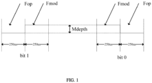
- a piece of data is sent every 500us, and data 1 and data 0 are sent in ways as shown in FIG. 1 .
- a communication signal sent from an energy transmitting terminal to an energy receiving terminal is transmitted by means of frequency conversion, and the problem lies in that in the PMA-3, PMA-4, PMA-5, PMA-6, PMA-7, and PMA-8 standard communication protocols, a communication carrier frequency Fop of a signal sent by an energy transmitting terminal (TX) is not unique (109KHz ⁇ Fop ⁇ 226KHz), and a frequency difference between Fop and Fmod is not fixed but only has a certain frequency difference range, i.e., having a modulation depth Mdepth (5 to 10 KHz), and thus the same power receiving system may need to simultaneously support the above six types of energy transmitting terminals (TX) based on different PMA protocols.
- a communication carrier frequency Fop of a signal sent by an energy transmitting terminal (TX) is not unique (109KHz ⁇ Fop ⁇ 226KHz)
- a frequency difference between Fop and Fmod is not fixed but only has a certain frequency difference range, i.e., having
- a signal received by an energy receiving terminal in a wireless charging system is an inductively coupled signal
- the received signal is not a single frequency sinusoidal signal, and instead, it may be doped with a large amount of high frequency noise.
- the traditional 2FSK demodulation methods are mainly three ways: coherent demodulation, filtering non-coherent demodulation and quadrature multiplication non-coherent demodulation.
- a difference value between a carrier frequency Fop and a modulation frequency Fmod is fixed within a certain range, such that the higher the frequency of Fop is, the smaller the cycle difference between Fop and Fmod is. If demodulation is done using traditional methods, the entire system requires very high precision to distinguish different frequencies, which will greatly increases the expenditure of the entire circuit no matter an analog manner or a digital manner is achieved.
- the carrier frequency Fop in the communication phase is not fixed to a certain value between 110 KHz and 205 KHz (the PMA protocol only provides a range), which may greatly increase the expenditure of the entire demodulation system.
- Prior art document CN 105 516 040 A discloses a low-consumption demodulation method for an FSK signal in wireless charging equipment.
- the method is characterized in that a signal on a receiving coil is sent to the input end of a demodulation chip comparator, and comprises the following steps of: (1) sampling an output value of the comparator and acquiring the number of sampled points in a period; (2) demodulating the signal according to the number of the sampled points in the period; (3) synthesizing a complete data frame according to a demodulated result; and (4) verifying and outputting the complete data frame.
- the low-consumption demodulation method which adopts the above steps and is used for the FSK signal in the wireless charging equipment, a complex analog circuit is not required, the maximum frequency required by a digital circuit in the method is only 2 MHz, , only a simple addition operation is performed under the frequency, and the main operating frequency is 210 KHz or below; and compared with a conventional FSK decoding method, the method is more suitable for the FSK signal according to the QI standard, the cost is low, the demodulation speed is high, debugging is convenient and the precision is high.
- An object of the present disclosure is to overcome the above-mentioned shortcomings of the prior art by providing a method for demodulating a frequency modulated signal of a PMA standard wireless charging device, which can reduce expenditure on a circuit caused by demodulation under a PMA standard communication protocol.
- the method for demodulating a frequency modulated signal of a PMA standard wireless charging device of the present disclosure is as follows.
- the main feature of the method for demodulating a frequency modulated signal of a PMA, Power Matters Alliance, standard wireless charging device is that the method mainly includes the following steps:
- a demodulation part does not require a complex analog circuit, and the highest frequency desired at a digital circuit part is only 4 MHz. Moreover, at this frequency, there is only a simple addition operation, and the main operating frequency is below 236 KHz. Compared with an existing FSK decoding method, the method is more compatible with a PMA standard frequency modulated signal, low in costs, high in demodulation speed, easy to adjust and high in accuracy, has no requirement for a fixed Fop, and can be widely applied.
- a method for demodulating a frequency modulated signal of a PMA standard wireless charging device includes the following steps:
- the step (1) specifically includes following steps:
- said filtering out a jitter waveform with a higher frequency in the outputted value of the comparator includes: filtering out a jitter waveform with a higher frequency in the outputted value of the comparator through a first low pass filter with a cutoff frequency of 5 kHz and a sampling frequency of 2 MHz.
- step (1-4) specifically includes following steps:
- the step (2) specifically includes the following steps:
- step (2-1) specifically includes the following steps:
- said eliminating frequency jitter caused by sampling includes: eliminating frequency jitter caused by sampling through a second low pass filter with a cutoff frequency of 8 kHz and a sampling frequency of 109 kHz.
- said counting Fop points includes executing a Fop point counting operation based on a differential method and executing a Fop point counting operation based on a right shifting method, and said executing a Fop point counting operation based on a differential method specifically includes following steps:
- Said executing a Fop point counting operation based on a right shifting method specifically includes following steps:
- step (2-5) includes the following steps:
- modifying sum_delta in a section smaller than the fourth constant specifically includes following steps:
- the step (3) includes the following steps:
- the step (3-3) includes the following steps:
- the step (3-4) includes the following steps:
- the disclosure abandons the conventional practice of the traditional 2FSK coherent demodulation and non-coherent demodulation, and according to the characteristics of the frequency modulation communication signal in the PMA standard, the analog circuit part uses only one comparator to replace the ADC sampling circuit, and at the same time, the digital part can achieve demodulation of the FSK signal only by using a clock frequency of 4 MHz.
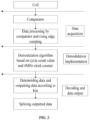
- the implementation process of the present disclosure is as shown in FIG. 2 .
- the outputted value of the comparator is read at 4MHz.
- the value can be regarded as 1bit sampling data of 4MHz.
- a low pass filter is applied to the data firstly so as to filter out the jitter waveform of higher frequency, and then demodulation and decoding processing is executed.
- the data acquisition process is shown in FIG. 3 .
- T_counter - - a cycle counter having a length of 6bit, which counts at a fixed frequency, outputs data at each rising edge and then clears to recount, without considering overflow issues during the counting process.
- the outputted value is stored in the cycle count buffer. After that, the subsequent processing is executed by taking a sum of members of the cycle count buffer- - SumTbuff as an object.
- SumTbuff is the sum of numbers of points of 23 cycles. Due to sampling and interference, SumTbuff data will inevitably fluctuate even in the case of a single-frequency signal.
- SumTbuff is used as an input signal, and a fluctuation of the sum of the numbers of the points can be regarded as a noise at a higher frequency.
- the fluctuation part of the sum of the numbers of the points in the SumTbuff is first smoothed by a low pass filter LPF2.
- the smoothed SumTbuff curve reflects a waveform of frequency, which is differentiated at this time. Meanwhile, the differential signal is subjected to a series of processing as shown in FIG. 4 , so as to eliminate the jitter and offset in the sum value with only the change value left for use in determination.
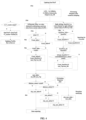
- the flowchart is shown in FIG. 5 .
- the outputted data in FIG. 4 is a sinusoidal-like waveform, and a 4 MHz clock count value between 2 zeros and non-zero transition points (zero to non-zero and non-zero to zero) is used as a basis for data determination.
- the 4MHz clock counter the clock is continuously counting, and the count value is fetched every time at the 0 and non-zero transition points of clip_sum_delta and then the count is restarted.
- a demodulation part does not require a complex analog circuit, and the highest frequency desired at a digital circuit part is only 4 MHz. Moreover, at this frequency, there is only a simple addition operation, and the main operating frequency is below 236 KHz. Compared with an existing FSK decoding method, the method is more compatible with a PMA standard frequency modulated signal, low in costs, high in demodulation speed, easy to adjust and high in accuracy, has no requirement for a fixed Fop, and can be widely applied.
Landscapes
- Engineering & Computer Science (AREA)
- Computer Networks & Wireless Communication (AREA)
- Signal Processing (AREA)
- Physics & Mathematics (AREA)
- Spectroscopy & Molecular Physics (AREA)
- Digital Transmission Methods That Use Modulated Carrier Waves (AREA)
- Compression, Expansion, Code Conversion, And Decoders (AREA)
- Mobile Radio Communication Systems (AREA)
Description
- The present disclosure relates to the field of wireless charging technologies, and in particular, to the field of wireless charging device communication technologies, and specifically to a method for demodulating a frequency modulated signal of a PMA standard wireless charging device.
- In a PMA standard wireless charging device, its energy transmitting terminal (TX) usually sends a FSK signal at the beginning of the whole system operation, and at this time, an operating frequency of a TX signal is from 215 KHz to 220 KHz in the PMA-3 system, from 142 KHz to 158 KHz in the PMA-4 and PMA-5 systems, from 109 KHz to 121 KHz in the PMA-6 system, from 140 KHz to 158 KHz in the PMA-7 system, and from 220 KHz to 226 KHz in the PMA-8 system. Fmod is Fop+Mdepth, and a value of a cycle difference Top-Tmod between a carrier frequency Fop and a modulation frequency Fmod can be calculated to be from 96 ns to 770ns. A piece of data is sent every 500us, and
data 1 anddata 0 are sent in ways as shown inFIG. 1 . - In the PMA (Power Matters Alliance) standard wireless charging device, a communication signal sent from an energy transmitting terminal to an energy receiving terminal is transmitted by means of frequency conversion, and the problem lies in that in the PMA-3, PMA-4, PMA-5, PMA-6, PMA-7, and PMA-8 standard communication protocols, a communication carrier frequency Fop of a signal sent by an energy transmitting terminal (TX) is not unique (109KHz ≤ Fop ≤ 226KHz), and a frequency difference between Fop and Fmod is not fixed but only has a certain frequency difference range, i.e., having a modulation depth Mdepth (5 to 10 KHz), and thus the same power receiving system may need to simultaneously support the above six types of energy transmitting terminals (TX) based on different PMA protocols.
- At the same time, since a signal received by an energy receiving terminal in a wireless charging system is an inductively coupled signal, the received signal is not a single frequency sinusoidal signal, and instead, it may be doped with a large amount of high frequency noise. The traditional 2FSK demodulation methods are mainly three ways: coherent demodulation, filtering non-coherent demodulation and quadrature multiplication non-coherent demodulation.
- Due to the limitation of the PMA standard communication protocol, a difference value between a carrier frequency Fop and a modulation frequency Fmod is fixed within a certain range, such that the higher the frequency of Fop is, the smaller the cycle difference between Fop and Fmod is. If demodulation is done using traditional methods, the entire system requires very high precision to distinguish different frequencies, which will greatly increases the expenditure of the entire circuit no matter an analog manner or a digital manner is achieved. At the same time, in different PMA transmission systems, the carrier frequency Fop in the communication phase is not fixed to a certain value between 110 KHz and 205 KHz (the PMA protocol only provides a range), which may greatly increase the expenditure of the entire demodulation system.
- Prior art document
CN 105 516 040 A discloses a low-consumption demodulation method for an FSK signal in wireless charging equipment. The method is characterized in that a signal on a receiving coil is sent to the input end of a demodulation chip comparator, and comprises the following steps of: (1) sampling an output value of the comparator and acquiring the number of sampled points in a period; (2) demodulating the signal according to the number of the sampled points in the period; (3) synthesizing a complete data frame according to a demodulated result; and (4) verifying and outputting the complete data frame. In the low-consumption demodulation method which adopts the above steps and is used for the FSK signal in the wireless charging equipment, a complex analog circuit is not required, the maximum frequency required by a digital circuit in the method is only 2 MHz, , only a simple addition operation is performed under the frequency, and the main operating frequency is 210 KHz or below; and compared with a conventional FSK decoding method, the method is more suitable for the FSK signal according to the QI standard, the cost is low, the demodulation speed is high, debugging is convenient and the precision is high. - An object of the present disclosure is to overcome the above-mentioned shortcomings of the prior art by providing a method for demodulating a frequency modulated signal of a PMA standard wireless charging device, which can reduce expenditure on a circuit caused by demodulation under a PMA standard communication protocol.
- In order to achieve the above object, the method for demodulating a frequency modulated signal of a PMA standard wireless charging device of the present disclosure is as follows.
- The main feature of the method for demodulating a frequency modulated signal of a PMA, Power Matters Alliance, standard wireless charging device is that the method mainly includes the following steps:
- (1) reading coil signals, sampling the coil signals, and counting sampling points in each cycle;
- (2) extracting a frequency change according to a change in a cycle count;
- (3) determining data according to the frequency change and a frequency duration and outputting the data; and
- (4) splicing the outputted data,
the step (2) specifically includes the following steps:- (2-1) calculating a sum of numbers of sampling points in latest 24 cycles according to a count value of the latest cycle;
- (2-2) filtering the sum of the numbers of the sampling points in the 24 cycles, and eliminating frequency jitter caused by sampling;
- (2-3) counting Fop points;
- (2-4) calculating sum_delta by the following formula:

- (2-5) eliminating the frequency jitter, modifying the waveform and outputting the modified waveform.
- With the method for demodulating a frequency modulated signal of a PMA standard wireless charging device of the present disclosure, a demodulation part does not require a complex analog circuit, and the highest frequency desired at a digital circuit part is only 4 MHz. Moreover, at this frequency, there is only a simple addition operation, and the main operating frequency is below 236 KHz. Compared with an existing FSK decoding method, the method is more compatible with a PMA standard frequency modulated signal, low in costs, high in demodulation speed, easy to adjust and high in accuracy, has no requirement for a fixed Fop, and can be widely applied.
-
-
FIG. 1 is a schematic diagram of a conventional FSK signal data transmission manner. -
FIG. 2 is a schematic diagram of a process of a method for demodulating a frequency modulated signal of a PMA standard wireless charging device according to the present disclosure. -
FIG. 3 is a flowchart of a data acquisition process of a method for demodulating a frequency modulated signal of a PMA standard wireless charging device according to the present disclosure. -
FIG. 4 is a flowchart of extracting a frequency change of a method for demodulating a frequency modulated signal of a PMA standard wireless charging device according to the present disclosure. -
FIG. 5 is a flowchart of data determination of a method for demodulating a frequency modulated signal of a wireless charging device according to the present disclosure. - In order to more clearly describe the technical content of the present disclosure, further description will be made below in conjunction with specific embodiments.
- In a feasible implementation manner, a method for demodulating a frequency modulated signal of a PMA standard wireless charging device includes the following steps:
- (1) reading coil signals, sampling the coil signals, and counting cycles;
- (2) extracting a frequency change according to a change in a cycle count;
- (3) determining data according to the frequency change and a frequency duration and outputting the data; and
- (4) splicing the outputted data.
- In a preferable implementation, the step (1) specifically includes following steps:
- (1-1) receiving the coil signals and comparing the coil signals with 0 level by a comparator;
- (1-2) reading an outputted value of the comparator at a frequency of 4 MHz;
- (1-3) filtering out a jitter waveform with a higher frequency in the outputted value of the comparator; and
- (1-4) counting the cycles by a cycle counter.
- In a preferred implementation, said filtering out a jitter waveform with a higher frequency in the outputted value of the comparator includes:
filtering out a jitter waveform with a higher frequency in the outputted value of the comparator through a first low pass filter with a cutoff frequency of 5 kHz and a sampling frequency of 2 MHz. - In a more preferred implementation, the step (1-4) specifically includes following steps:
- (1-4-1) determining whether the filtered outputted value of the comparator changes from 0 to 1 , and if yes, proceeding to step (1-4-2); otherwise, proceeding to step (1-4-3);
- (1-4-2) outputting a count value of the cycle counter, clearing the count value, and proceeding to step (1-1); and
- (1-4-3) incrementing the count value of the cycle counter by 1, and proceeding to step (1-1) .
- In the aforementioned feasible implementation, the step (2) specifically includes the following steps:
- (2-1) calculating a sum of numbers of sampling points in latest 24 cycles according to a count value of the latest cycle;
- (2-2) filtering the sum of the numbers of the sampling points in the 24 cycles, and eliminating frequency jitter caused by sampling;
- (2-3) counting Fop points;
- (2-4) calculating sum_delta by the following formula:

- (2-5) eliminating the frequency jitter, modifying the waveform and outputting the modified waveform.
- In a more preferred implementation, the step (2-1) specifically includes the following steps:
- (2-1-1) determining whether the cycle counter has an outputted value, and if yes, proceeding to step (2-1-2);
- (2-1-2) calculating the sum of the numbers of the sampling points in the 24 cycles according to the following formula:

- (2-1-2) updating the buffer Tbuffer.
- In a more preferred implementation, said eliminating frequency jitter caused by sampling includes:
eliminating frequency jitter caused by sampling through a second low pass filter with a cutoff frequency of 8 kHz and a sampling frequency of 109 kHz. - In a more preferred implementation, said counting Fop points includes executing a Fop point counting operation based on a differential method and executing a Fop point counting operation based on a right shifting method, and said executing a Fop point counting operation based on a differential method specifically includes following steps:
- (2-3-1) determining whether delta is 0, and if yes, proceeding to step (2-3-3), otherwise, proceeding to step (2-3-2), wherein delta is the differential result of the filtered outputted value ;
- (2-3-2) clearing Count_delta, wherein Count_delta is a count value when delta is 0, and proceeding to step (2-3-4);
- (2-3-3) incrementing Count_delta by 1 and proceeding to step (2-3-4);
- (2-3-4) determining whether Count_delta is greater than a first constant, and if yes, proceeding to step (2-3-5); and
- (2-3-5) clearing Count_delta, clearing Count_SumDiv4, taking a value of out_IIR as sum_Fop, and proceeding to step (2-4), wherein Count_SumDiv4 is a count value of SumDiv4, and SumDiv4 is a value obtained by right shifting the filtered outputted value by two bits.
- Said executing a Fop point counting operation based on a right shifting method specifically includes following steps:
- (2-3-a) determining whether a current SumDiv4 is equal to a previous SumDiv4, and if yes, proceeding to step (2-3-b), otherwise, proceeding to step (2-3-c);
- (2-3-b) incrementing Count_SumDiv4 by 1 and proceeding to step (2-3-d);
- (2-3-c) clearing Count_SumDiv4 and proceeding to step (2-3-d);
- (2-3-d) using the current SumDiv4 to cover the previous SumDiv4;
- (2-3-e) determining whether Count_SumDiv4 is greater than or equal to a second constant and whether an absolute value of sum_delta is greater than a third constant, and if yes, proceeding to step (2-3-f); and
- (2-3-f) clearing Count_SumDiv4, taking the value of out_IIR as sum_Fop, and proceeding to step (2-4).
- In a more preferred implementation, the step (2-5) includes the following steps:
- (2-5-1) determining whether an absolute value of sum_delta is smaller than or equal to a fourth constant, and if yes, proceeding to step (2-5-2), otherwise, proceeding to step (2-5-3);
- (2-5-2) taking clip_sum_delta= 0 as a modified sum_delta, and proceeding to step (2-5-4);
- (2-5-3) modifying sum_delta in a section smaller than the fourth constant, and proceeding to step (2-5-4); and
- (2-5-4) outputting data of the modified sum_delta.
- In a further implementation, modifying sum_delta in a section smaller than the fourth constant specifically includes following steps:
- (2-5-3-1) determining whether the absolute value of sum_delta is greater than 31, and if yes, proceeding to step (2-5-3-2), otherwise, proceeding to step (2-5-3-5);
- (2-5-3-2) determining whether sum_delta is greater than 0, and if yes, proceeding to step (2-5-3-3), otherwise, proceeding to step (2-5-3-4);
- (2-5-3-3) taking clip_sum_delta=31 as the modified sum_delta, and proceeding to step (2-5-4);
- (2-5-3-4) taking clip_sum_delta= -31 as the modified sum_delta, and proceeding to step (2-5-4); and
- (2-5-3-5) directly taking the value of sum_delta as clip_sum_delta, and proceeding to step (2-5-4).
- In a preferred implementation, the step (3) includes the following steps:
- (3-1) determining whether clip_sum_delta changes between zero and a non-zero value, and if yes, proceeding to step (3-2);
- (3-2) adding a value of clk_count to a value of reg_clk_count to obtain a new reg_clk_count, and clearing clk_count, where reg_clk_count is an accumulated value of a 4MHz clock counter, and clk_count is a count value of the 4MHz clock counter;
- (3-3) performing data determination on reg_clk_count to obtain data_bit;
- (3-4) outputting data according to data_bit; and
- (3-5) outputting data, saving a latest bit_salve, and proceeding to step (4), wherein the outputted data is 0 or 1, bit_salve is a saved value of the data determination, and the saved value of the data determination is used to save a condition of a latest determined half cycle.
- In a more preferred implementation, the step (3-3) includes the following steps:
- (3-3-1) determining whether reg_clk_count is greater than or equal to a predetermined threshold value, and if yes, proceeding to step (3-3-2), otherwise, proceeding to step (3-3-3);
- (3-3-2) clearing reg_clk_count, outputting a data determination result as data_bit = 8, and proceeding to step (4);
- (3-3-3) determining whether clip_sum_delta changes from a non-zero value to zero, and if yes, proceeding to step (3-3-4), otherwise, proceeding to step (3-3-8);
- (3-3-4) determining whether reg_clk_count is greater than the threshold value const_a, and if yes, proceeding to step (3-3-5), otherwise, proceeding to step (3-3-6);
- (3-3-5) skipping the determination and proceeding to step (3-4);
- (3-3-6) determining whether bit_salve is equal to 3, and if yes, recording the data determination result as case a, otherwise, recording the data determination result as case b;
- (3-3-7) subtracting a threshold value const_d from a value of reg_clk_count to obtain a new reg_clk_count, and proceeding to step (3-4);
- (3-3-8) determining whether reg_clk_count is smaller than a threshold value const_e, and if yes, recording the data determination result as case c and proceeding to step (3-3-9), otherwise, proceeding to step (3-3-10);
- (3-3-9) clearing reg_clk_count, and proceeding to step (3-4);
- (3-3-10) determining whether reg_clk_count is smaller than a threshold value const_d, and if yes, proceeding to step (3-3-11), otherwise, proceeding to step (3-3-12);
- (3-3-11) determining whether bit_salve is equal to 2, and if yes, recording the data determination result as case d, otherwise, recording the data determination result as case e, and proceeding to step (3-3-9);
- (3-3-12) determining whether reg_clk_count is smaller than a threshold value const_c, and if yes, proceeding to step (3-3-13), otherwise, proceeding to step (3-3-15);
- (3-3-13) determining whether bit_salve is equal to 2, and if yes, recording the data determination result as case f and proceeding to step (3-3-9), otherwise, proceeding to step (3-3-14);
- (3-3-14) determining whether bit_salve is equal to 3, and if yes, recording the data determination result as case g, otherwise, recording the data determination result as case h, and proceeding to the step (3-3-9);
- (3-3-15) determining whether reg_clk_count is smaller than the threshold value const_b, and if yes, proceeding to step (3-3-16), otherwise, recording the data determination result as case m and proceeding to the step (3-3-9) ;
- (3-3-16) determining whether bit_salve is equal to 2, and if yes, recording the data determination result as case j and proceeding to the step (3-3-9), otherwise, proceeding to step (3-3-17); and
- (3-3-17) determining whether bit_salve is equal to 3, and if yes, recording the data determination result as case k, otherwise, recording the data determination result as
case 1, and proceeding to the step (3-3-9). - In a preferable implementation, the step (3-4) includes the following steps:
- (3-4-1) determining whether data_bit is equal to 8, and if yes, proceeding to step (3-4-2), otherwise, proceeding to step (3-4-3);
- (3-4-2) clearing reg_clk_count;
- (3-4-3) determining a value of data_bit; and
- (3-4-4) ascertaining the outputted data according to the value of data_bit, saving a latest bit_salve, the outputted data being 0 or 1, and proceeding to step (4).
- The disclosure abandons the conventional practice of the traditional 2FSK coherent demodulation and non-coherent demodulation, and according to the characteristics of the frequency modulation communication signal in the PMA standard, the analog circuit part uses only one comparator to replace the ADC sampling circuit, and at the same time, the digital part can achieve demodulation of the FSK signal only by using a clock frequency of 4 MHz. The implementation process of the present disclosure is as shown in
FIG. 2 . - In a medium power wireless charging communication protocol, since the method in which a transmitting terminal generates a sinusoidal wave is controlled by PWM, this method makes it easier to control the frequency and duty cycle of the outputted signal and also causes the signal spectrum to be complex, which cannot be demodulated by the general FSK method. Since the duty cycle of the PWM modulation method is changing while its cycle is fixed and unchanged, the present design obtains coded data by detecting the number of points in the signal cycle and processing the number of the points as a signal. This algorithm fixes a sum of 24 cycles as a processing object, and outputs the sum of the most recent 24 cycle counts every time an end of one cycle is detected. Then, data determination is executed based on the change trend of the sum value in combination with a 4 MHz clock counter.
- After the signal on the coil enters into the chip and is compared with the 0 level by a comparator, the outputted value of the comparator is read at 4MHz. The value can be regarded as 1bit sampling data of 4MHz. In order to ensure that the jitter of the waveform of the input signal will not affect the subsequent decoding algorithm, a low pass filter is applied to the data firstly so as to filter out the jitter waveform of higher frequency, and then demodulation and decoding processing is executed. The data acquisition process is shown in
FIG. 3 . - The following is a name of a variable and meaning it represents in the decoding process:
T_counter - - a cycle counter having a length of 6bit, which counts at a fixed frequency, outputs data at each rising edge and then clears to recount, without considering overflow issues during the counting process. - 2) Extracting the frequency change according to the change in the sum of numbers of points in cycles:
the flowchart is shown inFIG. 4 . - Parameters will be described as follows:
- const1, const2, const3, const4 - - constants involved in the algorithm;
- Tbuffer - - a cycle count buffer, which is used for saving an outputted value of T_counter has a depth of 23, first in first out;
- SumTbuff - - a sum of members of the cycle count buffer, 15bit, having an initial value of 0;
- delta - a differential result of outputted values by LPF2;
- Count_delta - - a counter when a delta value is 0, which accumulates when delta is 0 and clears when there is a change;
- sum_delta - - a difference between the sum values, indicating a difference between a value currently outputted by the filter and a current Fop value; and
- clip_sum_delta - - modified sum_delta data.
- If the counter T_counter has an output, the outputted value is stored in the cycle count buffer. After that, the subsequent processing is executed by taking a sum of members of the cycle count buffer- - SumTbuff as an object.
- SumTbuff is the sum of numbers of points of 23 cycles. Due to sampling and interference, SumTbuff data will inevitably fluctuate even in the case of a single-frequency signal. Here, SumTbuff is used as an input signal, and a fluctuation of the sum of the numbers of the points can be regarded as a noise at a higher frequency.
- Therefore, in the whole process, the fluctuation part of the sum of the numbers of the points in the SumTbuff is first smoothed by a low pass filter LPF2.
- The smoothed SumTbuff curve reflects a waveform of frequency, which is differentiated at this time. Meanwhile, the differential signal is subjected to a series of processing as shown in
FIG. 4 , so as to eliminate the jitter and offset in the sum value with only the change value left for use in determination. - The flowchart is shown in
FIG. 5 . The outputted data inFIG. 4 is a sinusoidal-like waveform, and a 4 MHz clock count value between 2 zeros and non-zero transition points (zero to non-zero and non-zero to zero) is used as a basis for data determination. In the 4MHz clock counter, the clock is continuously counting, and the count value is fetched every time at the 0 and non-zero transition points of clip_sum_delta and then the count is restarted. - Parameters will be described as follows:
- const_a, const_b, const_c, const_d, const_e - - threshold values of a 4MHz clock counter involved in the algorithm;
- clip_sum_delta - - an output of a cycle point number processing module;
- clk_count - - a 4MHz clock counter;
- reg_clk_count - - an output register of a 4MHz counter;
- data_bit - - 0 indicating that 0 is detected, 1 indicating that 1 is detected, 2 indicating that fop + fmod + fop is detected, 3 indicating that fmod + fop + fop is detected, 4 indicating that fop + fmod + fop is detected, 5 indicating that fmod + fop +long fop is detected, 6 indicating that fop+fmod+long fop is detected, 7 indicating that the processing is suspending, and 8 indicating that an error is detected; and
- bit_salve - - a data determination saving value for saving the latest determined half cycle, 2 indicating fop, 3 indicating fmod, and 0 and 1 indicating that the previous data has been determined.
- According to the disclosure, a demodulation part does not require a complex analog circuit, and the highest frequency desired at a digital circuit part is only 4 MHz. Moreover, at this frequency, there is only a simple addition operation, and the main operating frequency is below 236 KHz. Compared with an existing FSK decoding method, the method is more compatible with a PMA standard frequency modulated signal, low in costs, high in demodulation speed, easy to adjust and high in accuracy, has no requirement for a fixed Fop, and can be widely applied.
- In this specification, the disclosure has been described with reference to specific embodiments thereof. However, it will be apparent that various modifications and changes can be made without departing from the scope of the disclosure. Accordingly, the specification and drawings should be regarded as illustrative rather than limiting, the scope of the invention being defined by the appended claims.
Claims (12)
- A method for demodulating a frequency modulated signal of a PMA, Power Matters Alliance, standard wireless charging device, wherein the method comprises following steps:1) reading coil signals, sampling the coil signals, and counting sampling points in each cycle;2) extracting a frequency change according to a change in a cycle count;3) determining data according to the frequency change and a frequency duration and outputting the data; and4) splicing the outputted data,wherein the step 2) specifically comprises following steps:2-1) calculating a sum of numbers of sampling points in latest 24 cycles according to a count value of the latest cycle;2-2) filtering the sum of the numbers of the sampling points in the 24 cycles, and eliminating frequency jitter caused by sampling;2-3) determining a value sum_Fop corresponding to the operation frequency Fop;2-4) calculating sum_delta by the following formula:
 2-5) performing processing on sum_delta in order to eliminate jitter and offset and to output a modified sum_delta for use in determining data.
 - The method for demodulating a frequency modulated signal of a PMA standard wireless charging device according to claim 1, characterized in that the step 1) specifically comprises following steps:1-1) receiving the coil signals and comparing the coil signals with 0 level by a comparator;1-2) sampling an outputted value of the comparator at a frequency of 4 MHz;1-3) filtering out a jitter waveform with a higher frequency in sampling points output by the comparator; and1-4) counting sampling points in each cycle by a sample counter.
- The method for demodulating a frequency modulated signal of a PMA standard wireless charging device according to claim 2, characterized in that said filtering out a jitter waveform with a higher frequency in the outputted value of the comparator comprises:
filtering out a jitter waveform with a higher frequency in the outputted value of the comparator through a first low pass filter with a cutoff frequency of 5 kHz and a sampling frequency of 2 MHz. - The method for demodulating a frequency modulated signal of a PMA standard wireless charging device according to claim 2, characterized in that the step 1-4) specifically comprises following steps:1-4-1) determining whether the filtered outputted value of the comparator changes from 0 to 1, and if yes, proceeding to step 1-4-2); otherwise, proceeding to step 1-4-3);1-4-2) outputting a count value of the sample counter, clearing the count value, and proceeding to step 1-1); and1-4-3) incrementing the count value of the sample counter by 1, and proceeding to step 1-1).
- The method for demodulating a frequency modulated signal of a PMA standard wireless charging device according to claim 1, characterized in that the step 2-1) specifically comprises following steps:2-1-1) determining whether the sample counter has an outputted value, and if yes, proceeding to step 2-1-2);2-1-2) calculating the sum of the numbers of the sampling points in the 24 cycles according to the following formula:
 2-1-2) updating the buffer Tbuffer.
 - The method for demodulating a frequency modulated signal of a PMA standard wireless charging device according to claim 1, characterized in that said eliminating frequency jitter caused by sampling comprises:
eliminating frequency jitter caused by sampling through a second low pass filter with a cutoff frequency of 8 kHz and a sampling frequency of 109 kHz. - The method for demodulating a frequency modulated signal of a PMA standard wireless charging device according to claim 1, characterized in that counting Fop points comprises executing a Fop point counting operation based on a differential method and executing a Fop point counting operation based on a right shifting method, and said executing a Fop point counting operation based on a differential method specifically comprises following steps:2-3-1) determining whether delta is 0, and if yes, proceeding to step 2-3-3), otherwise, proceeding to step 2-3-2), wherein delta is a differential result of the filtered outputted value;2-3-2) clearing Count_delta, wherein Count_delta is a count value when delta is 0, and proceeding to step 2-3-4);2-3-3) incrementing Count_delta by 1 and proceeding to step 2-3-4);2-3-4) determining whether Count_delta is greater than a first constant, and if yes, proceeding to step 2-3-5); and2-3-5) clearing Count_delta, clearing Count_SumDiv4, taking a value of out_IIR as sum_Fop, and proceeding to step 2-4), where Count_SumDiv4 is a count value of SumDiv4, and SumDiv4 is a value obtained by right shifting the filtered outputted value by two bits,wherein said executing a Fop point counting operation based on a right shifting method specifically comprises following steps:2-3-a) determining whether a current SumDiv4 is equal to a previous SumDiv4, and if yes, proceeding to step 2-3-b), otherwise, proceeding to step 2-3-c);2-3-b) incrementing Count_SumDiv4 by 1 and proceeding to step 2-3-d);2-3-c) clearing Count_SumDiv4 and proceeding to step 2-3-d);2-3-d) using the current SumDiv4 to cover the previous SumDiv4;2-3-e) determining whether Count_SumDiv4 is greater than or equal to a second constant and whether an absolute value of sum_delta is greater than a third constant, and if yes, proceeding to step 2-3-f); and2-3-f) clearing Count_SumDiv4, taking the value of out_IIR as sum_Fop, and proceeding to step 2-4).
- The method for demodulating a frequency modulated signal of a PMA standard wireless charging device according to claim 1, characterized in that the step 2-5) comprises following steps:2-5-1) determining whether an absolute value of sum_delta is smaller than or equal to a fourth constant, and if yes, proceeding to step 2-5-2), otherwise, proceeding to step 2-5-3);2-5-2) taking clip_sum_delta= 0 as a modified sum_delta, and proceeding to step 2-5-4);2-5-3) modifying sum_delta in a section smaller than the fourth constant, and proceeding to step 2-5-4); and2-5-4) outputting data of the modified sum_delta.
- The method for demodulating a frequency modulated signal of a PMA standard wireless charging device according to claim 8, characterized in that said modifying sum_delta in a section smaller than the fourth constant specifically comprises following steps:2-5-3-1) determining whether the absolute value of sum_delta is greater than 31, and if yes, proceeding to step 2-5-3-2), otherwise, proceeding to step 2-5-3-5);2-5-3-2) determining whether sum_delta is greater than 0, and if yes, proceeding to step 2-5-3-3), otherwise, proceeding to step 2-5-3-4);2-5-3-3) taking clip_sum_delta=31 as the modified sum_delta, and proceeding to step 2-5-4);2-5-3-4) taking clip_sum_delta= -31 as the modified sum_delta, and proceeding to step 2-5-4); and2-5-3-5) directly taking the value of sum_delta as clip_sum_delta, and proceeding to step 2-5-4).
- The method for demodulating a frequency modulated signal of a PMA standard wireless charging device according to claim 1, characterized in that the step 3) comprises following steps:3-1) determining whether clip_sum_delta changes between zero and a non-zero value, and if yes, proceeding to step 3-2);3-2) adding a value of clk_count to a value of reg_clk_count to obtain a new reg_clk_count, and clearing clk_count, where reg_clk_count is an accumulated value of a 4MHz clock counter, and clk_count is a count value of the 4MHz clock counter;3-3) performing data determination on reg_clk_count to obtain data_bit;3-4) outputting data according to data_bit; and3-5) outputting data, saving a latest bit_salve, and proceeding to step 4), wherein the outputted data is 0 or 1, bit_salve is a saved value of the data determination, and the saved value of the data determination is used to save a condition of a latest determined half cycle.
- The method for demodulating a frequency modulated signal of a PMA standard wireless charging device according to claim 10, characterized in that the step 3-3) comprises following steps:3-3-1) determining whether reg_clk_count is greater than or equal to a predetermined threshold value, and if yes, proceeding to step 3-3-2), otherwise, proceeding to step 3-3-3);3-3-2) clearing reg_clk_count, outputting a data determination result as data_bit = 8, and proceeding to step 4);3-3-3) determining whether clip_sum_delta changes from a non-zero value to zero, and if yes, proceeding to step 3-3-4), otherwise, proceeding to step 3-3-8);3-3-4) determining whether reg_clk_count is greater than a threshold value const_a, and if yes, proceeding to step 3-3-5), otherwise, proceeding to step 3-3-6);3-3-5) skipping the determination and proceeding to step 3-4);3-3-6) determining whether bit_salve is equal to 3, and if yes, recording the data determination result as case a, otherwise, recording the data determination result as case b;3-3-7) subtracting a threshold value const_d from a value of reg_clk_count to obtain a new reg_clk_count, and proceeding to step 3-4);3-3-8) determining whether reg_clk_count is smaller than a threshold value const_e, and if yes, recording the data determination result as case c and proceeding to step 3-3-9), otherwise, proceeding to step 3-3-10);3-3-9) clearing reg_clk_count, and proceeding to step 3-4);3-3-10) determining whether reg_clk_count is smaller than a threshold value const_d, and if yes, proceeding to step 3-3-11), otherwise, proceeding to step 3-3-12);3-3-11) determining whether bit_salve is equal to 2, and if yes, recording the data determination result as case d, otherwise, recording the data determination result as case e, and proceeding to step 3-3-9);3-3-12) determining whether reg_clk_count is smaller than a threshold value const_c, and if yes, proceeding to step 3-3-13), otherwise, proceeding to step 3-3-15);3-3-13) determining whether bit_salve is equal to 2, and if yes, recording the data determination result as case f and proceeding to step 3-3-9), otherwise, proceeding to step 3-3-14);3-3-14) determining whether bit_salve is equal to 3, and if yes, recording the data determination result as case g, otherwise, recording the data determination result as case h, and proceeding to the step 3-3-9);3-3-15) determining whether reg_clk_count is smaller than the threshold value const_b, and if yes, proceeding to step 3-3-16), otherwise, recording the data determination result as case m and proceeding to the step 3-3-9) ;3-3-16) determining whether bit_salve is equal to 2, and if yes, recording the data determination result as case j and proceeding to the step 3-3-9), otherwise, proceeding to step 3-3-17); and3-3-17) determining whether bit_salve is equal to 3, and if yes, recording the data determination result as case k, otherwise, recording the data determination result as case 1, and proceeding to the step 3-3-9).
- The method for demodulating a frequency modulated signal of a PMA standard wireless charging device according to claim 10, characterized in that the step 3-4) comprises following steps:3-4-1) determining whether data_bit is equal to 8, and if yes, proceeding to step 3-4-2), otherwise, proceeding to step 3-4-3);3-4-2) clearing reg_clk_count;3-4-3) determining a value of data_bit; and3-4-4) ascertaining the outputted data according to the value of data_bit, saving a latest bit_salve, the outputted data being 0 or 1, and proceeding to step 4).
Applications Claiming Priority (2)
| Application Number | Priority Date | Filing Date | Title |
|---|---|---|---|
| CN201610954140.1A CN106534015B (en) | 2016-11-03 | 2016-11-03 | For the demodulation method of the wireless charging device FM signal of PMA standards |
| PCT/CN2017/095076 WO2018082356A1 (en) | 2016-11-03 | 2017-07-29 | Method for demodulating frequency modulation signal of pma standard wireless charging device |
Publications (4)
| Publication Number | Publication Date |
|---|---|
| EP3537675A1 EP3537675A1 (en) | 2019-09-11 |
| EP3537675A4 EP3537675A4 (en) | 2020-10-21 |
| EP3537675B1 true EP3537675B1 (en) | 2023-06-07 |
| EP3537675C0 EP3537675C0 (en) | 2023-06-07 |
Family
ID=58325447
Family Applications (1)
| Application Number | Title | Priority Date | Filing Date |
|---|---|---|---|
| EP17866497.5A Active EP3537675B1 (en) | 2016-11-03 | 2017-07-29 | Method for demodulating an fsk signal of a pma standard wireless charging device |
Country Status (4)
| Country | Link |
|---|---|
| US (1) | US10708096B2 (en) |
| EP (1) | EP3537675B1 (en) |
| CN (1) | CN106534015B (en) |
| WO (1) | WO2018082356A1 (en) |
Families Citing this family (9)
| Publication number | Priority date | Publication date | Assignee | Title |
|---|---|---|---|---|
| CN106532969B (en) * | 2016-11-03 | 2018-06-12 | 无锡华润矽科微电子有限公司 | The circuit structure that fsk signal efficiently demodulates is realized in wireless charging device |
| CN106534015B (en) | 2016-11-03 | 2018-02-09 | 无锡华润矽科微电子有限公司 | For the demodulation method of the wireless charging device FM signal of PMA standards |
| CN108933748B (en) * | 2017-05-27 | 2020-12-18 | 无锡华润矽科微电子有限公司 | Method and system for demodulating frequency-modulated signal capable of locking frequency change |
| CN110896311B (en) * | 2018-08-22 | 2021-05-18 | 华润微集成电路(无锡)有限公司 | Decoding circuit of wireless charging equipment frequency modulation signal aiming at PMA standard |
| CN109639396B (en) * | 2018-12-19 | 2021-03-16 | 惠科股份有限公司 | Data transmission method and device and computer readable storage medium |
| CN109474308B (en) * | 2018-12-19 | 2021-07-09 | 深圳易联凯科技有限公司 | Signal demodulation system and method |
| CN111541507B (en) * | 2020-04-20 | 2021-12-14 | 吉林省广播电视研究所(吉林省广播电视局科技信息中心) | Frequency measuring type frequency modulation stereo demodulation system of single chip microcomputer |
| CN112152955B (en) * | 2020-09-24 | 2022-03-04 | 华润微集成电路(无锡)有限公司 | Method for realizing FSK decoding based on wireless charging system |
| CN114553389B (en) * | 2022-02-24 | 2023-06-16 | 中电科申泰信息科技有限公司 | Novel self-adaptive verification method for high-speed data radio self-adaptive interface |
Citations (1)
| Publication number | Priority date | Publication date | Assignee | Title |
|---|---|---|---|---|
| IT201600111351A1 (en) * | 2016-11-04 | 2018-05-04 | St Microelectronics Des & Appl | PROCEDURE FOR REVEALING SIGNALS WITH FSK MODULATION, CIRCUIT, DEVICE AND CORRESPONDENT COMPUTER PRODUCT |
Family Cites Families (12)
| Publication number | Priority date | Publication date | Assignee | Title |
|---|---|---|---|---|
| US5416481A (en) * | 1993-09-24 | 1995-05-16 | Advanced Micro Devices, Inc. | Analog-to-digital converter with multi-level dither current input |
| US6417802B1 (en) * | 2000-04-26 | 2002-07-09 | Litton Systems, Inc. | Integrated inertial/GPS navigation system |
| US7881409B2 (en) * | 2004-01-22 | 2011-02-01 | The Regents Of The University Of Michigan | Demodulator, chip and method for digitally demodulating an FSK signal |
| US7015716B2 (en) * | 2004-04-13 | 2006-03-21 | Feature Integration Technology Inc. | Method for detecting a power load of a power supply module according to duty cycle detection, and related device |
| JP4707556B2 (en) * | 2005-12-28 | 2011-06-22 | Okiセミコンダクタ株式会社 | FSK signal generator |
| EP2769540B1 (en) * | 2011-10-20 | 2018-11-28 | Dolby Laboratories Licensing Corporation | Method and system for video equalization |
| CN104617884B (en) * | 2013-11-04 | 2017-09-15 | 无锡华润矽科微电子有限公司 | A kind of wireless charging digital demodulating circuit and method |
| CN103855764B (en) * | 2014-01-14 | 2016-05-18 | 深圳市普林泰克科技有限公司 | Mobile device detection method on a kind of wireless charger emission end surface |
| CN105897639B (en) * | 2014-12-09 | 2020-06-16 | 恩智浦美国有限公司 | FSK demodulator |
| CN106506420B (en) * | 2015-09-08 | 2021-02-09 | 恩智浦美国有限公司 | Wireless charger using frequency-aliased FSK demodulation |
| CN105516040B (en) * | 2015-11-30 | 2019-01-08 | 无锡华润矽科微电子有限公司 | The low consumption demodulation method of fsk signal in wireless charging device |
| CN106534015B (en) * | 2016-11-03 | 2018-02-09 | 无锡华润矽科微电子有限公司 | For the demodulation method of the wireless charging device FM signal of PMA standards |
-
2016
- 2016-11-03 CN CN201610954140.1A patent/CN106534015B/en active Active
-
2017
- 2017-07-29 US US16/337,513 patent/US10708096B2/en active Active
- 2017-07-29 EP EP17866497.5A patent/EP3537675B1/en active Active
- 2017-07-29 WO PCT/CN2017/095076 patent/WO2018082356A1/en not_active Ceased
Patent Citations (2)
| Publication number | Priority date | Publication date | Assignee | Title |
|---|---|---|---|---|
| IT201600111351A1 (en) * | 2016-11-04 | 2018-05-04 | St Microelectronics Des & Appl | PROCEDURE FOR REVEALING SIGNALS WITH FSK MODULATION, CIRCUIT, DEVICE AND CORRESPONDENT COMPUTER PRODUCT |
| US20180131544A1 (en) * | 2016-11-04 | 2018-05-10 | Stmicroelectronics Design And Application S.R.O. | Method of detecting fsk-modulated signals, corresponding circuit, device and computer program product |
Also Published As
| Publication number | Publication date |
|---|---|
| EP3537675A1 (en) | 2019-09-11 |
| US20190253288A1 (en) | 2019-08-15 |
| EP3537675C0 (en) | 2023-06-07 |
| WO2018082356A1 (en) | 2018-05-11 |
| CN106534015B (en) | 2018-02-09 |
| US10708096B2 (en) | 2020-07-07 |
| EP3537675A4 (en) | 2020-10-21 |
| CN106534015A (en) | 2017-03-22 |
Similar Documents
| Publication | Publication Date | Title |
|---|---|---|
| US10708096B2 (en) | Method for demodulating frequency modulated signal of PMA standard wireless charging device | |
| CN105516040B (en) | The low consumption demodulation method of fsk signal in wireless charging device | |
| CN103837740A (en) | High-precision digital instantaneous frequency measurement method and device | |
| US10700903B2 (en) | Circuit structure for efficiently demodulating FSK signal in wireless charging device | |
| CN106487425B (en) | The demodulation method of fsk signal in wireless charging device | |
| US20170070265A1 (en) | Wireless charger using frequency aliasing fsk demodulation | |
| CN108512791A (en) | Satellite-borne AIS demodulation method based on timing frequency offset compensation | |
| US11860200B2 (en) | Zero crossing point signal output and power line data transmitting method and device | |
| CN106487424B (en) | The demodulator circuit of fsk signal in wireless charging device | |
| CN105791204A (en) | A method and device for all-digital envelope detection and demodulation of AC IRIG-B codes | |
| CN114338329B (en) | Implementation methods, devices, equipment and media for detecting communication integrated waveforms | |
| CN113271276B (en) | Signal demodulation decoding method and device and computer readable storage medium | |
| CN1187941C (en) | Baseband data slicing method and apparatus | |
| CN116248454B (en) | Multi-modulation signal blind detection and identification method, device, computer equipment and medium | |
| CN108768909B (en) | 2FSK symbol synchronization method and system based on minimum variance | |
| CN108933748B (en) | Method and system for demodulating frequency-modulated signal capable of locking frequency change | |
| CN102075470A (en) | (Gauss) frequency shift keying ((G)FSK) digital demodulation device and method | |
| CN114266264B (en) | Signal demodulation method, device, receiver and computer-readable storage medium | |
| CN109698803B (en) | Circuit structure for realizing FSK signal high-efficiency demodulation in wireless charging equipment | |
| CN103166599B (en) | Low-power-consumption matched filtering method used for distinguishing existing of signal | |
| JP2017085347A (en) | Signal processing apparatus and communication apparatus | |
| TWI636684B (en) | Signal transceiver synchronization point detection method | |
| CN112688892B (en) | Subcarrier detection method, carrier signal demodulation method and demodulation device | |
| WO2020038363A1 (en) | Decoding circuit for frequency modulation signal of pma standard wireless charging device | |
| US20260100871A1 (en) | Decoder circuit, corresponding receiver and transmission system |
Legal Events
| Date | Code | Title | Description |
|---|---|---|---|
| STAA | Information on the status of an ep patent application or granted ep patent |
Free format text: STATUS: THE INTERNATIONAL PUBLICATION HAS BEEN MADE |
|
| PUAI | Public reference made under article 153(3) epc to a published international application that has entered the european phase |
Free format text: ORIGINAL CODE: 0009012 |
|
| STAA | Information on the status of an ep patent application or granted ep patent |
Free format text: STATUS: REQUEST FOR EXAMINATION WAS MADE |
|
| 17P | Request for examination filed |
Effective date: 20190329 |
|
| AK | Designated contracting states |
Kind code of ref document: A1 Designated state(s): AL AT BE BG CH CY CZ DE DK EE ES FI FR GB GR HR HU IE IS IT LI LT LU LV MC MK MT NL NO PL PT RO RS SE SI SK SM TR |
|
| AX | Request for extension of the european patent |
Extension state: BA ME |
|
| DAV | Request for validation of the european patent (deleted) | ||
| DAX | Request for extension of the european patent (deleted) | ||
| RIC1 | Information provided on ipc code assigned before grant |
Ipc: H04L 27/156 20060101AFI20200616BHEP Ipc: H04B 5/00 20060101ALI20200616BHEP Ipc: H04L 25/49 20060101ALN20200616BHEP |
|
| A4 | Supplementary search report drawn up and despatched |
Effective date: 20200923 |
|
| RIC1 | Information provided on ipc code assigned before grant |
Ipc: H04L 27/156 20060101AFI20200917BHEP Ipc: H04B 5/00 20060101ALI20200917BHEP Ipc: H04L 25/49 20060101ALN20200917BHEP |
|
| RAP3 | Party data changed (applicant data changed or rights of an application transferred) |
Owner name: CRM ICBG (WUXI) CO., LTD. |
|
| REG | Reference to a national code |
Ref country code: DE Ref legal event code: R079 Ref document number: 602017069971 Country of ref document: DE Free format text: PREVIOUS MAIN CLASS: H04L0027148000 Ipc: H04L0027156000 |
|
| GRAP | Despatch of communication of intention to grant a patent |
Free format text: ORIGINAL CODE: EPIDOSNIGR1 |
|
| RIC1 | Information provided on ipc code assigned before grant |
Ipc: H04L 25/49 20060101ALN20221010BHEP Ipc: H04B 5/00 20060101ALI20221010BHEP Ipc: H04L 27/156 20060101AFI20221010BHEP |
|
| STAA | Information on the status of an ep patent application or granted ep patent |
Free format text: STATUS: GRANT OF PATENT IS INTENDED |
|
| INTG | Intention to grant announced |
Effective date: 20221117 |
|
| RIC1 | Information provided on ipc code assigned before grant |
Ipc: H04L 25/49 20060101ALN20221108BHEP Ipc: H04B 5/00 20060101ALI20221108BHEP Ipc: H04L 27/156 20060101AFI20221108BHEP |
|
| GRAS | Grant fee paid |
Free format text: ORIGINAL CODE: EPIDOSNIGR3 |
|
| GRAA | (expected) grant |
Free format text: ORIGINAL CODE: 0009210 |
|
| STAA | Information on the status of an ep patent application or granted ep patent |
Free format text: STATUS: THE PATENT HAS BEEN GRANTED |
|
| AK | Designated contracting states |
Kind code of ref document: B1 Designated state(s): AL AT BE BG CH CY CZ DE DK EE ES FI FR GB GR HR HU IE IS IT LI LT LU LV MC MK MT NL NO PL PT RO RS SE SI SK SM TR |
|
| REG | Reference to a national code |
Ref country code: GB Ref legal event code: FG4D |
|
| REG | Reference to a national code |
Ref country code: CH Ref legal event code: EP Ref country code: AT Ref legal event code: REF Ref document number: 1578096 Country of ref document: AT Kind code of ref document: T Effective date: 20230615 |
|
| REG | Reference to a national code |
Ref country code: DE Ref legal event code: R096 Ref document number: 602017069971 Country of ref document: DE |
|
| U01 | Request for unitary effect filed |
Effective date: 20230627 |
|
| U07 | Unitary effect registered |
Designated state(s): AT BE BG DE DK EE FI FR IT LT LU LV MT NL PT SE SI Effective date: 20230804 |
|
| U20 | Renewal fee for the european patent with unitary effect paid |
Year of fee payment: 7 Effective date: 20230804 |
|
| REG | Reference to a national code |
Ref country code: LT Ref legal event code: MG9D |
|
| PG25 | Lapsed in a contracting state [announced via postgrant information from national office to epo] |
Ref country code: NO Free format text: LAPSE BECAUSE OF FAILURE TO SUBMIT A TRANSLATION OF THE DESCRIPTION OR TO PAY THE FEE WITHIN THE PRESCRIBED TIME-LIMIT Effective date: 20230907 Ref country code: ES Free format text: LAPSE BECAUSE OF FAILURE TO SUBMIT A TRANSLATION OF THE DESCRIPTION OR TO PAY THE FEE WITHIN THE PRESCRIBED TIME-LIMIT Effective date: 20230607 |
|
| PG25 | Lapsed in a contracting state [announced via postgrant information from national office to epo] |
Ref country code: RS Free format text: LAPSE BECAUSE OF FAILURE TO SUBMIT A TRANSLATION OF THE DESCRIPTION OR TO PAY THE FEE WITHIN THE PRESCRIBED TIME-LIMIT Effective date: 20230607 Ref country code: HR Free format text: LAPSE BECAUSE OF FAILURE TO SUBMIT A TRANSLATION OF THE DESCRIPTION OR TO PAY THE FEE WITHIN THE PRESCRIBED TIME-LIMIT Effective date: 20230607 Ref country code: GR Free format text: LAPSE BECAUSE OF FAILURE TO SUBMIT A TRANSLATION OF THE DESCRIPTION OR TO PAY THE FEE WITHIN THE PRESCRIBED TIME-LIMIT Effective date: 20230908 |
|
| PG25 | Lapsed in a contracting state [announced via postgrant information from national office to epo] |
Ref country code: SK Free format text: LAPSE BECAUSE OF FAILURE TO SUBMIT A TRANSLATION OF THE DESCRIPTION OR TO PAY THE FEE WITHIN THE PRESCRIBED TIME-LIMIT Effective date: 20230607 |
|
| PG25 | Lapsed in a contracting state [announced via postgrant information from national office to epo] |
Ref country code: IS Free format text: LAPSE BECAUSE OF FAILURE TO SUBMIT A TRANSLATION OF THE DESCRIPTION OR TO PAY THE FEE WITHIN THE PRESCRIBED TIME-LIMIT Effective date: 20231007 |
|
| PG25 | Lapsed in a contracting state [announced via postgrant information from national office to epo] |
Ref country code: SM Free format text: LAPSE BECAUSE OF FAILURE TO SUBMIT A TRANSLATION OF THE DESCRIPTION OR TO PAY THE FEE WITHIN THE PRESCRIBED TIME-LIMIT Effective date: 20230607 Ref country code: SK Free format text: LAPSE BECAUSE OF FAILURE TO SUBMIT A TRANSLATION OF THE DESCRIPTION OR TO PAY THE FEE WITHIN THE PRESCRIBED TIME-LIMIT Effective date: 20230607 Ref country code: RO Free format text: LAPSE BECAUSE OF FAILURE TO SUBMIT A TRANSLATION OF THE DESCRIPTION OR TO PAY THE FEE WITHIN THE PRESCRIBED TIME-LIMIT Effective date: 20230607 Ref country code: IS Free format text: LAPSE BECAUSE OF FAILURE TO SUBMIT A TRANSLATION OF THE DESCRIPTION OR TO PAY THE FEE WITHIN THE PRESCRIBED TIME-LIMIT Effective date: 20231007 Ref country code: CZ Free format text: LAPSE BECAUSE OF FAILURE TO SUBMIT A TRANSLATION OF THE DESCRIPTION OR TO PAY THE FEE WITHIN THE PRESCRIBED TIME-LIMIT Effective date: 20230607 |
|
| PG25 | Lapsed in a contracting state [announced via postgrant information from national office to epo] |
Ref country code: PL Free format text: LAPSE BECAUSE OF FAILURE TO SUBMIT A TRANSLATION OF THE DESCRIPTION OR TO PAY THE FEE WITHIN THE PRESCRIBED TIME-LIMIT Effective date: 20230607 |
|
| REG | Reference to a national code |
Ref country code: CH Ref legal event code: PL |
|
| REG | Reference to a national code |
Ref country code: DE Ref legal event code: R097 Ref document number: 602017069971 Country of ref document: DE |
|
| PG25 | Lapsed in a contracting state [announced via postgrant information from national office to epo] |
Ref country code: MC Free format text: LAPSE BECAUSE OF FAILURE TO SUBMIT A TRANSLATION OF THE DESCRIPTION OR TO PAY THE FEE WITHIN THE PRESCRIBED TIME-LIMIT Effective date: 20230607 |
|
| PG25 | Lapsed in a contracting state [announced via postgrant information from national office to epo] |
Ref country code: MC Free format text: LAPSE BECAUSE OF FAILURE TO SUBMIT A TRANSLATION OF THE DESCRIPTION OR TO PAY THE FEE WITHIN THE PRESCRIBED TIME-LIMIT Effective date: 20230607 |
|
| PLBE | No opposition filed within time limit |
Free format text: ORIGINAL CODE: 0009261 |
|
| STAA | Information on the status of an ep patent application or granted ep patent |
Free format text: STATUS: NO OPPOSITION FILED WITHIN TIME LIMIT |
|
| REG | Reference to a national code |
Ref country code: IE Ref legal event code: MM4A |
|
| PG25 | Lapsed in a contracting state [announced via postgrant information from national office to epo] |
Ref country code: CH Free format text: LAPSE BECAUSE OF NON-PAYMENT OF DUE FEES Effective date: 20230731 |
|
| 26N | No opposition filed |
Effective date: 20240308 |
|
| GBPC | Gb: european patent ceased through non-payment of renewal fee |
Effective date: 20230907 |
|
| PG25 | Lapsed in a contracting state [announced via postgrant information from national office to epo] |
Ref country code: IE Free format text: LAPSE BECAUSE OF NON-PAYMENT OF DUE FEES Effective date: 20230729 |
|
| PG25 | Lapsed in a contracting state [announced via postgrant information from national office to epo] |
Ref country code: GB Free format text: LAPSE BECAUSE OF NON-PAYMENT OF DUE FEES Effective date: 20230907 |
|
| U20 | Renewal fee for the european patent with unitary effect paid |
Year of fee payment: 8 Effective date: 20240612 |
|
| PG25 | Lapsed in a contracting state [announced via postgrant information from national office to epo] |
Ref country code: IE Free format text: LAPSE BECAUSE OF NON-PAYMENT OF DUE FEES Effective date: 20230729 Ref country code: GB Free format text: LAPSE BECAUSE OF NON-PAYMENT OF DUE FEES Effective date: 20230907 |
|
| PG25 | Lapsed in a contracting state [announced via postgrant information from national office to epo] |
Ref country code: CY Free format text: LAPSE BECAUSE OF FAILURE TO SUBMIT A TRANSLATION OF THE DESCRIPTION OR TO PAY THE FEE WITHIN THE PRESCRIBED TIME-LIMIT; INVALID AB INITIO Effective date: 20170729 |
|
| U20 | Renewal fee for the european patent with unitary effect paid |
Year of fee payment: 9 Effective date: 20250625 |
|
| PG25 | Lapsed in a contracting state [announced via postgrant information from national office to epo] |
Ref country code: HU Free format text: LAPSE BECAUSE OF FAILURE TO SUBMIT A TRANSLATION OF THE DESCRIPTION OR TO PAY THE FEE WITHIN THE PRESCRIBED TIME-LIMIT; INVALID AB INITIO Effective date: 20170729 |
|
| PG25 | Lapsed in a contracting state [announced via postgrant information from national office to epo] |
Ref country code: TR Free format text: LAPSE BECAUSE OF FAILURE TO SUBMIT A TRANSLATION OF THE DESCRIPTION OR TO PAY THE FEE WITHIN THE PRESCRIBED TIME-LIMIT Effective date: 20230607 |