EP3537479A1 - Flexible display - Google Patents
Flexible display Download PDFInfo
- Publication number
- EP3537479A1 EP3537479A1 EP18736181.1A EP18736181A EP3537479A1 EP 3537479 A1 EP3537479 A1 EP 3537479A1 EP 18736181 A EP18736181 A EP 18736181A EP 3537479 A1 EP3537479 A1 EP 3537479A1
- Authority
- EP
- European Patent Office
- Prior art keywords
- supporting film
- flexible display
- region
- flexible
- bonding region
- Prior art date
- Legal status (The legal status is an assumption and is not a legal conclusion. Google has not performed a legal analysis and makes no representation as to the accuracy of the status listed.)
- Granted
Links
Images


Classifications
-
- H—ELECTRICITY
- H10—SEMICONDUCTOR DEVICES; ELECTRIC SOLID-STATE DEVICES NOT OTHERWISE PROVIDED FOR
- H10K—ORGANIC ELECTRIC SOLID-STATE DEVICES
- H10K77/00—Constructional details of devices covered by this subclass and not covered by groups H10K10/80, H10K30/80, H10K50/80 or H10K59/80
- H10K77/10—Substrates, e.g. flexible substrates
- H10K77/111—Flexible substrates
-
- H—ELECTRICITY
- H10—SEMICONDUCTOR DEVICES; ELECTRIC SOLID-STATE DEVICES NOT OTHERWISE PROVIDED FOR
- H10K—ORGANIC ELECTRIC SOLID-STATE DEVICES
- H10K59/00—Integrated devices, or assemblies of multiple devices, comprising at least one organic light-emitting element covered by group H10K50/00
- H10K59/80—Constructional details
- H10K59/87—Passivation; Containers; Encapsulations
- H10K59/871—Self-supporting sealing arrangements
-
- H—ELECTRICITY
- H10—SEMICONDUCTOR DEVICES; ELECTRIC SOLID-STATE DEVICES NOT OTHERWISE PROVIDED FOR
- H10W—GENERIC PACKAGES, INTERCONNECTIONS, CONNECTORS OR OTHER CONSTRUCTIONAL DETAILS OF DEVICES COVERED BY CLASS H10
- H10W70/00—Package substrates; Interposers; Redistribution layers [RDL]
- H10W70/60—Insulating or insulated package substrates; Interposers; Redistribution layers
-
- H—ELECTRICITY
- H10—SEMICONDUCTOR DEVICES; ELECTRIC SOLID-STATE DEVICES NOT OTHERWISE PROVIDED FOR
- H10W—GENERIC PACKAGES, INTERCONNECTIONS, CONNECTORS OR OTHER CONSTRUCTIONAL DETAILS OF DEVICES COVERED BY CLASS H10
- H10W90/00—Package configurations
-
- H—ELECTRICITY
- H10—SEMICONDUCTOR DEVICES; ELECTRIC SOLID-STATE DEVICES NOT OTHERWISE PROVIDED FOR
- H10K—ORGANIC ELECTRIC SOLID-STATE DEVICES
- H10K2102/00—Constructional details relating to the organic devices covered by this subclass
- H10K2102/301—Details of OLEDs
- H10K2102/311—Flexible OLED
-
- H—ELECTRICITY
- H10—SEMICONDUCTOR DEVICES; ELECTRIC SOLID-STATE DEVICES NOT OTHERWISE PROVIDED FOR
- H10K—ORGANIC ELECTRIC SOLID-STATE DEVICES
- H10K2102/00—Constructional details relating to the organic devices covered by this subclass
- H10K2102/301—Details of OLEDs
- H10K2102/351—Thickness
-
- H—ELECTRICITY
- H10—SEMICONDUCTOR DEVICES; ELECTRIC SOLID-STATE DEVICES NOT OTHERWISE PROVIDED FOR
- H10K—ORGANIC ELECTRIC SOLID-STATE DEVICES
- H10K59/00—Integrated devices, or assemblies of multiple devices, comprising at least one organic light-emitting element covered by group H10K50/00
- H10K59/80—Constructional details
-
- H—ELECTRICITY
- H10—SEMICONDUCTOR DEVICES; ELECTRIC SOLID-STATE DEVICES NOT OTHERWISE PROVIDED FOR
- H10K—ORGANIC ELECTRIC SOLID-STATE DEVICES
- H10K59/00—Integrated devices, or assemblies of multiple devices, comprising at least one organic light-emitting element covered by group H10K50/00
- H10K59/80—Constructional details
- H10K59/87—Passivation; Containers; Encapsulations
- H10K59/873—Encapsulations
-
- Y—GENERAL TAGGING OF NEW TECHNOLOGICAL DEVELOPMENTS; GENERAL TAGGING OF CROSS-SECTIONAL TECHNOLOGIES SPANNING OVER SEVERAL SECTIONS OF THE IPC; TECHNICAL SUBJECTS COVERED BY FORMER USPC CROSS-REFERENCE ART COLLECTIONS [XRACs] AND DIGESTS
- Y02—TECHNOLOGIES OR APPLICATIONS FOR MITIGATION OR ADAPTATION AGAINST CLIMATE CHANGE
- Y02E—REDUCTION OF GREENHOUSE GAS [GHG] EMISSIONS, RELATED TO ENERGY GENERATION, TRANSMISSION OR DISTRIBUTION
- Y02E10/00—Energy generation through renewable energy sources
- Y02E10/50—Photovoltaic [PV] energy
- Y02E10/549—Organic PV cells
-
- Y—GENERAL TAGGING OF NEW TECHNOLOGICAL DEVELOPMENTS; GENERAL TAGGING OF CROSS-SECTIONAL TECHNOLOGIES SPANNING OVER SEVERAL SECTIONS OF THE IPC; TECHNICAL SUBJECTS COVERED BY FORMER USPC CROSS-REFERENCE ART COLLECTIONS [XRACs] AND DIGESTS
- Y02—TECHNOLOGIES OR APPLICATIONS FOR MITIGATION OR ADAPTATION AGAINST CLIMATE CHANGE
- Y02P—CLIMATE CHANGE MITIGATION TECHNOLOGIES IN THE PRODUCTION OR PROCESSING OF GOODS
- Y02P70/00—Climate change mitigation technologies in the production process for final industrial or consumer products
- Y02P70/50—Manufacturing or production processes characterised by the final manufactured product
Definitions
- the present application relates to the field of display technologies, particularly to a flexible display.
- OLED displays draw much attention as next-generation display devices applied to mobile electronic devices.
- a glass substrate is used in an OLED display, it is inconvenient to carry the OLED display due to the fragility and poor flexibility of the glass substrate which consequently limits the development of the OLED display to some extent. Therefore, a flexible OLED display is developed by using a flexible substrate (for example, plastic).
- the flexible OLED display has good flexibility and can be folded or wound to be conveniently carried, overcoming the disadvantages of an ordinary OLED display.
- a flexible display mainly includes a flexible display screen and a drive chip, where the flexible display screen includes a flexible substrate comprising a display region and a bonding region, and the drive chip is bonded to the bonding region.
- thickness of a flexible display screen is very small, usually about 0.02 mm. Therefore, when the drive chip is bonded to the bonding region, the flexible display screen is likely to be warped, resulting in quality degradation of the flexible display screen, or it is difficult for a vacuum cup to suck the flexible display screen, resulting in difficulty in a bonding operation.
- An object of the present application is to provide a flexible display, to resolve problems, such as a flexible display screen being likely to be warped during drive chip bonding or being difficult to be bonded in an existing flexible display manufacturing process.
- the present application provides a flexible display, including: a flexible display screen and a drive chip, wherein the flexible display screen includes a flexible substrate comprising a display region and a bonding region, a supporting film is adhered to a back of the flexible substrate, and a drive chip is bonded to the bonding region.
- each of the display region and the bonding region is provided with supporting film, wherein the supporting film in the display region is viscous and the supporting film in the bonding region is removable.
- a supporting film is adhered to the display region and the bonding region has no supporting film.
- a supporting film is adhered to each of the display region and the bonding region, where the supporting film in the bonding region has holes formed therein, and the supporting film in the display region has no hole.
- a supporting film is adhered to each of the display region and the bonding region, where the supporting film in each of the bonding region and the display region has holes formed therein, and a hole ratio of the supporting film in the bonding region is higher than that of the supporting film in the display region.
- the supporting film in the bonding region is more flexible than in the display region.
- the thickness of the supporting film ranges from 0.1 ⁇ m to 0.3 ⁇ m.
- the supporting film is made of a material same as a material of the flexible substrate.
- the supporting film is made of resins.
- the flexible display screen further includes a driver circuit unit located on the front of the flexible substrate; an organic light emitting element located on the front of the flexible substrate and connected to the drive circuit unit; a film sealant covering the organic light emitting element; and a water and oxygen barrier layer covering the film sealant.
- the supporting film is adhered to the back of the flexible substrate, improving rigidity of the flexible display screen to some extent, so that the flexible display screen is unlikely to be warped when a drive chip is bonded thereto and can be easily sucked by a vacuum cup to facilitate bonding, during the flexible display manufacturing process.
- the bonding region has no supporting film, or the supporting film in the bonding region is more flexible than in the display region. That is, on one hand, the flexible display screen is unlikely to be warped when a drive chip is bonded thereto and can be easily sucked by a vacuum cup to facilitate bonding during the flexible display manufacturing process, and on the other hand, the bonding region is enabled to be easily bent to satisfy the bending requirement for the entire flexible display.
- the core idea of the present application is to provide a flexible display, where a supporting film is adhered to the back of the flexible substrate of the flexible display, which can improve rigidity of the flexible display screen to some extent, so that the flexible display screen is unlikely to be warped when a drive chip is bonded thereto and can be easily sucked by a vacuum cup to facilitate bonding, during a flexible display manufacturing process.
- the bonding region has no supporting film, or the supporting film in the bonding region is more flexible than in the display region.
- the flexible display screen is unlikely to be warped when a drive chip is bonded thereto and can be easily sucked by a vacuum cup to facilitate bonding, during the flexible display manufacturing process, and on the other hand, the bonding region is enabled to be easily bent to satisfy the bending requirement for the entire flexible display.
- the flexible display 1 includes a flexible display screen 10 and a drive chip 20, where the flexible display screen 10 includes a flexible substrate 11 comprising a display region and a bonding region, a supporting film 12 is adhered to the back of the flexible substrate 11, and the drive chip 20 is bonded to the bonding region.
- the support film 12 is adhered to the back of the flexible substrate 11 to improve rigidity of the flexible display screen 10 to some extent, so that the flexible display screen 10 is unlikely to be warped when a drive chip is bonded thereto, and can be easily sucked by a vacuum cup to facilitate bonding during a flexible display manufacturing process.
- a supporting film is adhered to the display region, and the bonding region has no supporting film.
- the flexible display has a higher bending requirement for the bonding region than for the display region. That is, the bonding region needs to have a higher degree of curvature.
- a supporting film is adhered to the display region, and the bonding region has no support film, so that on one hand the flexible display screen 10 is unlikely to be warped when a drive chip is bonded thereto and can be easily sucked by a vacuum cup to facilitate bonding during the flexible display manufacturing process, and on the other hand, the bonding region can be enabled to have excellent bending performance to satisfy the high bending requirement for the bonding region.
- the bonding region in a bending condition can be referred to in FIG. 2 .
- the supporting film 12 is made of resins.
- the resins have excellent flexibility, so that the flexible substrate 11 to which the supporting film 12 is adhered keeps a good flexibility.
- the supporting film 12 is made of a material same as the material of the flexible substrate 11, so that the connection between the supporting film 12 and the flexible substrate 11 is firmer and more stable.
- thickness of the supporting film 12 ranges from 0.1 ⁇ m to 0.3 ⁇ m.
- thickness of the supporting film 12 may be 0.1 ⁇ m, 0.125 ⁇ m, 0.15 ⁇ m, 0.175 ⁇ m, 0.2 ⁇ m, 0.215 ⁇ m, 0.25 ⁇ m, 0.275 ⁇ m, or 0.3 ⁇ m, etc.
- thickness of the supporting film 12 selectively ranges from 0.1 ⁇ m to 0.3 ⁇ m, so that on one hand the flexible display screen 10 is unlikely to be warped when a drive chip is bonded thereto and can be easily sucked by a vacuum cup to facilitate bonding during the flexible display manufacturing process, and on the other hand, the bending requirement for the bonding region can be satisfied.
- the flexible display 1 further includes a driver circuit unit 13 located on the front of the flexible substrate 11; an organic light emitting element 14 located on the front of the flexible substrate 11 and connected to the driver circuit unit 13; a film sealant 15 covering the organic light emitting element 14; and a water and oxygen barrier layer 16 covering the film sealant 15.
- the water and oxygen barrier layer includes a water and oxygen barrier adhesive 160 covering the film sealant 15 and a water and oxygen barrier film 161 covering the water and oxygen barrier adhesive 160.
- the supporting film 12 is adhered to the flexible substrate 11 in the following manner.
- an original supporting film 12' having a separator line 120 is provided and the separator line 120 divides the original supporting film 12' into a first portion 121 and a second portion 122.
- the front of the first portion 121 is viscous and the front of the second portion 122 is non-viscous.
- the drive chip 20 is bonded to the bonding region, as shown in FIG. 5 .
- the second portion 122 of the original supporting film is removed along the separator line 120.
- the first portion 121 of the original supporting film is adhered to the back of the flexible substrate 11, correspondingly referring to FIG. 1 . That is, the supporting film 12 is only adhered to the display region.
- the original supporting film 12' may be adhered to the flexible substrate 11 without having the second portion 122 removed when manufacturing the flexible display.
- each of the display region and the bonding region of the obtained flexible display is provided with the supporting film, where the supporting film in the display region (that is, the first portion) is viscous and the supporting film in the bonding region (that is, the second portion) is removable.
- the supporting film in the bonding region of the flexible display can either be retained or removed in subsequent use, thereby increasing application flexibility.
- Embodiment 2 differs from Embodiment 1 in that: in Embodiment 1, the bonding region has no supporting film, or the supporting film in the bonding region is removable, and can be selectively retained or removed as needed; however, in Embodiment 2, the supporting film is adhered to each of the display region and the bonding region, wherein the supporting film in the bonding region has holes while the supporting film in the display region has no hole, or the supporting film in each of the bonding region and the display region has holes while the hole ratio of the supporting film in the bonding region is higher than in the display region.
- FIG. 6 a schematic structural diagram of the supporting film in Embodiment 2 of the present application.
- the supporting film 32 is provided with a separator line 320 dividing the supporting film 32 into a first portion 321 and a second portion 322.
- the front of the first portion 321 and the second portion 322 are both viscous.
- both the first portion 321 and the second portion 322 have holes. Furthermore, there are multiple holes on each of the first portion 321 and the second portion 322, the multiple holes on each of the first portion 321 are regularly spaced apart, the multiple holes on each of the second portion 322 are regularly spaced apart.
- the hole ratio of the first portion 321 is lower than that of the second portion 322.
- hole ratio is the ratio of the hole area to non-hole area. Specifically, the area of pores 324 on the second portion 322 is larger, and the spacing between adjacent pores 324 is smaller. The area of pores 323 on the first portion 321 is smaller, and the spacing between adjacent pores 323 is also small. That is, in this embodiment of the present application, the second portion 322 is more flexible than the first portion 321.
- the supporting film 32 is adhered to the back of the flexible substrate, wherein the first portion 321 corresponds to the display region and the second portion 322 corresponds to the bonding region.
- a drive chip is bonded to the bonding region to obtain a flexible display.
- the supporting film in the bonding region is no longer removed. That is, a supporting film having holes is adhered to the bonding region, and a supporting film having holes is adhered to the display region with the hole ratio of the supporting film adhered to the display region being lower than that of the supporting film adhered to the bonding region. In other words, the supporting film adhered to the display region is less flexible than the supporting film adhered to the bonding region.
- the flexible display screen is unlikely to be warped when a drive chip is bonded thereto and can be easily sucked by a vacuum cup to facilitate bonding during a flexible display manufacturing process, and on the other hand, the bonding region is able to have excellent bending performance to satisfy a high bending requirement for the bonding region.
Landscapes
- Electroluminescent Light Sources (AREA)
- Devices For Indicating Variable Information By Combining Individual Elements (AREA)
Abstract
Description
- The present application relates to the field of display technologies, particularly to a flexible display.
- Organic Light Emitting Diode (OLED) displays draw much attention as next-generation display devices applied to mobile electronic devices. However, if a glass substrate is used in an OLED display, it is inconvenient to carry the OLED display due to the fragility and poor flexibility of the glass substrate which consequently limits the development of the OLED display to some extent. Therefore, a flexible OLED display is developed by using a flexible substrate (for example, plastic). The flexible OLED display has good flexibility and can be folded or wound to be conveniently carried, overcoming the disadvantages of an ordinary OLED display.
- A flexible display mainly includes a flexible display screen and a drive chip, where the flexible display screen includes a flexible substrate comprising a display region and a bonding region, and the drive chip is bonded to the bonding region. At present, thickness of a flexible display screen is very small, usually about 0.02 mm. Therefore, when the drive chip is bonded to the bonding region, the flexible display screen is likely to be warped, resulting in quality degradation of the flexible display screen, or it is difficult for a vacuum cup to suck the flexible display screen, resulting in difficulty in a bonding operation.
- An object of the present application is to provide a flexible display, to resolve problems, such as a flexible display screen being likely to be warped during drive chip bonding or being difficult to be bonded in an existing flexible display manufacturing process.
- To resolve the above technical problems, the present application provides a flexible display, including: a flexible display screen and a drive chip, wherein the flexible display screen includes a flexible substrate comprising a display region and a bonding region, a supporting film is adhered to a back of the flexible substrate, and a drive chip is bonded to the bonding region.
- Optionally, in the flexible display, each of the display region and the bonding region is provided with supporting film, wherein the supporting film in the display region is viscous and the supporting film in the bonding region is removable.
- Optionally, in the flexible display, a supporting film is adhered to the display region and the bonding region has no supporting film.
- Optionally, in the flexible display, a supporting film is adhered to each of the display region and the bonding region, where the supporting film in the bonding region has holes formed therein, and the supporting film in the display region has no hole.
- Optionally, in the flexible display, a supporting film is adhered to each of the display region and the bonding region, where the supporting film in each of the bonding region and the display region has holes formed therein, and a hole ratio of the supporting film in the bonding region is higher than that of the supporting film in the display region.
- Optionally, in the flexible display, the supporting film in the bonding region is more flexible than in the display region.
- Optionally, in the flexible display, the thickness of the supporting film ranges from 0.1 µm to 0.3 µm.
- Optionally, in the flexible display, the supporting film is made of a material same as a material of the flexible substrate.
- Optionally, in the flexible display, the supporting film is made of resins.
- Optionally, in the flexible display, the flexible display screen further includes a driver circuit unit located on the front of the flexible substrate; an organic light emitting element located on the front of the flexible substrate and connected to the drive circuit unit; a film sealant covering the organic light emitting element; and a water and oxygen barrier layer covering the film sealant.
- In the flexible display provided in the present application, the supporting film is adhered to the back of the flexible substrate, improving rigidity of the flexible display screen to some extent, so that the flexible display screen is unlikely to be warped when a drive chip is bonded thereto and can be easily sucked by a vacuum cup to facilitate bonding, during the flexible display manufacturing process. Particularly, the bonding region has no supporting film, or the supporting film in the bonding region is more flexible than in the display region. That is, on one hand, the flexible display screen is unlikely to be warped when a drive chip is bonded thereto and can be easily sucked by a vacuum cup to facilitate bonding during the flexible display manufacturing process, and on the other hand, the bonding region is enabled to be easily bent to satisfy the bending requirement for the entire flexible display.
-
-
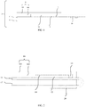
FIG. 1 is a schematic structural diagram of a flexible display according to Embodiment 1 of the present application; -
FIG. 2 is a schematic diagram of a partially bended flexible display according to Embodiment 1 of the present application; -
FIG. 3 is a schematic structural diagram of an original supporting film used in Embodiment 1 of the present application; -
FIG. 4 and FIG. 5 are schematic diagrams of a process of adhering a supporting film to a flexible substrate and bonding a drive chip to the flexible substrate in Embodiment 1 of the present application; and -
FIG. 6 is a schematic structural diagram of a supporting film used in Embodiment 2 of the present application. - The flexible display provided in the present application is described below in more detail with reference to the accompanying drawings and specific embodiments. The advantages and features of the present application are more apparent according to the following descriptions and claims. It should be noted that the accompanying drawings are provided in a very simplified form not necessarily presented to scale, with the only intention of facilitating convenience and clarity in explaining a few illustrative examples of the present application.
- The core idea of the present application is to provide a flexible display, where a supporting film is adhered to the back of the flexible substrate of the flexible display, which can improve rigidity of the flexible display screen to some extent, so that the flexible display screen is unlikely to be warped when a drive chip is bonded thereto and can be easily sucked by a vacuum cup to facilitate bonding, during a flexible display manufacturing process. Particularly, the bonding region has no supporting film, or the supporting film in the bonding region is more flexible than in the display region. That is, on one hand, the flexible display screen is unlikely to be warped when a drive chip is bonded thereto and can be easily sucked by a vacuum cup to facilitate bonding, during the flexible display manufacturing process, and on the other hand, the bonding region is enabled to be easily bent to satisfy the bending requirement for the entire flexible display.
- Refer to
FIG. 1 , a schematic structural diagram of a flexible display according to Embodiment 1 of the present application. As shown inFIG. 1 , the flexible display 1 includes aflexible display screen 10 and adrive chip 20, where theflexible display screen 10 includes aflexible substrate 11 comprising a display region and a bonding region, a supportingfilm 12 is adhered to the back of theflexible substrate 11, and thedrive chip 20 is bonded to the bonding region. Thesupport film 12 is adhered to the back of theflexible substrate 11 to improve rigidity of theflexible display screen 10 to some extent, so that theflexible display screen 10 is unlikely to be warped when a drive chip is bonded thereto, and can be easily sucked by a vacuum cup to facilitate bonding during a flexible display manufacturing process. - Continue to refer to
FIG. 1 , in this embodiment of the present application, a supporting film is adhered to the display region, and the bonding region has no supporting film. Usually, the flexible display has a higher bending requirement for the bonding region than for the display region. That is, the bonding region needs to have a higher degree of curvature. Therefore, in this embodiment of the present application, a supporting film is adhered to the display region, and the bonding region has no support film, so that on one hand theflexible display screen 10 is unlikely to be warped when a drive chip is bonded thereto and can be easily sucked by a vacuum cup to facilitate bonding during the flexible display manufacturing process, and on the other hand, the bonding region can be enabled to have excellent bending performance to satisfy the high bending requirement for the bonding region. The bonding region in a bending condition can be referred to inFIG. 2 . - Preferably, the supporting
film 12 is made of resins. The resins have excellent flexibility, so that theflexible substrate 11 to which the supportingfilm 12 is adhered keeps a good flexibility. More preferably, the supportingfilm 12 is made of a material same as the material of theflexible substrate 11, so that the connection between the supportingfilm 12 and theflexible substrate 11 is firmer and more stable. - Further, thickness of the supporting
film 12 ranges from 0.1µm to 0.3µm. For example, thickness of the supportingfilm 12 may be 0.1 µm, 0.125 µm, 0.15 µm, 0.175 µm, 0.2 µm, 0.215 µm, 0.25 µm, 0.275 µm, or 0.3 µm, etc. In this embodiment of the present application, thickness of the supportingfilm 12 selectively ranges from 0.1 µm to 0.3 µm, so that on one hand theflexible display screen 10 is unlikely to be warped when a drive chip is bonded thereto and can be easily sucked by a vacuum cup to facilitate bonding during the flexible display manufacturing process, and on the other hand, the bending requirement for the bonding region can be satisfied. - Continue to refer to
FIG. 1 , the flexible display 1 further includes adriver circuit unit 13 located on the front of theflexible substrate 11; an organiclight emitting element 14 located on the front of theflexible substrate 11 and connected to thedriver circuit unit 13; afilm sealant 15 covering the organiclight emitting element 14; and a water andoxygen barrier layer 16 covering thefilm sealant 15. In this embodiment of the present application, the water and oxygen barrier layer includes a water and oxygen barrier adhesive 160 covering thefilm sealant 15 and a water andoxygen barrier film 161 covering the water and oxygen barrier adhesive 160. - In this embodiment of the present application, the supporting
film 12 is adhered to theflexible substrate 11 in the following manner. - Firstly, as shown in
FIG. 3 , an original supporting film 12' having aseparator line 120 is provided and theseparator line 120 divides the original supporting film 12' into afirst portion 121 and asecond portion 122. The front of thefirst portion 121 is viscous and the front of thesecond portion 122 is non-viscous. - Subsequently, as shown in
FIG. 4 , the front of the original supportingfilm 12 is adhered to the back of theflexible substrate 11. - In this embodiment of the present application, after the original supporting film 12' is adhered to the
flexible substrate 11, thedrive chip 20 is bonded to the bonding region, as shown inFIG. 5 . - Finally, the
second portion 122 of the original supporting film is removed along theseparator line 120. In this case, only thefirst portion 121 of the original supporting film is adhered to the back of theflexible substrate 11, correspondingly referring toFIG. 1 . That is, the supportingfilm 12 is only adhered to the display region. - In another embodiment of the present application, alternatively, the original supporting film 12' may be adhered to the
flexible substrate 11 without having thesecond portion 122 removed when manufacturing the flexible display. In this embodiment, each of the display region and the bonding region of the obtained flexible display is provided with the supporting film, where the supporting film in the display region (that is, the first portion) is viscous and the supporting film in the bonding region (that is, the second portion) is removable. The supporting film in the bonding region of the flexible display can either be retained or removed in subsequent use, thereby increasing application flexibility. - Embodiment 2 differs from Embodiment 1 in that: in Embodiment 1, the bonding region has no supporting film, or the supporting film in the bonding region is removable, and can be selectively retained or removed as needed; however, in Embodiment 2, the supporting film is adhered to each of the display region and the bonding region, wherein the supporting film in the bonding region has holes while the supporting film in the display region has no hole, or the supporting film in each of the bonding region and the display region has holes while the hole ratio of the supporting film in the bonding region is higher than in the display region.
- Take the supporting film in each of the bonding region and the display region having holes as example. Specifically, referring to
FIG. 6 , a schematic structural diagram of the supporting film in Embodiment 2 of the present application. As shown inFIG. 2 , the supportingfilm 32 is provided with aseparator line 320 dividing the supportingfilm 32 into afirst portion 321 and asecond portion 322. The front of thefirst portion 321 and thesecond portion 322 are both viscous. - Further, both the
first portion 321 and thesecond portion 322 have holes. Furthermore, there are multiple holes on each of thefirst portion 321 and thesecond portion 322, the multiple holes on each of thefirst portion 321 are regularly spaced apart, the multiple holes on each of thesecond portion 322 are regularly spaced apart. The hole ratio of thefirst portion 321 is lower than that of thesecond portion 322. Herein, hole ratio is the ratio of the hole area to non-hole area. Specifically, the area ofpores 324 on thesecond portion 322 is larger, and the spacing betweenadjacent pores 324 is smaller. The area ofpores 323 on thefirst portion 321 is smaller, and the spacing betweenadjacent pores 323 is also small. That is, in this embodiment of the present application, thesecond portion 322 is more flexible than thefirst portion 321. - Subsequently, the supporting
film 32 is adhered to the back of the flexible substrate, wherein thefirst portion 321 corresponds to the display region and thesecond portion 322 corresponds to the bonding region. Next, a drive chip is bonded to the bonding region to obtain a flexible display. In this embodiment of the present application, the supporting film in the bonding region is no longer removed. That is, a supporting film having holes is adhered to the bonding region, and a supporting film having holes is adhered to the display region with the hole ratio of the supporting film adhered to the display region being lower than that of the supporting film adhered to the bonding region. In other words, the supporting film adhered to the display region is less flexible than the supporting film adhered to the bonding region. Hence, on one hand, the flexible display screen is unlikely to be warped when a drive chip is bonded thereto and can be easily sucked by a vacuum cup to facilitate bonding during a flexible display manufacturing process, and on the other hand, the bonding region is able to have excellent bending performance to satisfy a high bending requirement for the bonding region. - The foregoing descriptions are merely descriptions of the preferred embodiments of the present application rather than any limitations to the scope of the present application. Any variations or modifications made by those of ordinary skilled in the art according to the foregoing disclosure fall within the scope of the appended claims.
Claims (10)
- A flexible display, comprising: a flexible display screen and a drive chip, wherein the flexible display screen comprises a flexible substrate including a display region and a bonding region, the back of the flexible substrate is adhered with a supporting film and the drive chip is bonded to the bonding region.
- The flexible display according to claim 1, wherein the display region and the bonding region are respectively provided with the supporting film, the supporting film provided in the display region is viscous, and the supporting film provided in the bonding region is removable.
- The flexible display according to claim 1, wherein the supporting film is adhered to the display region and the bonding region has no supporting film.
- The flexible display according to claim 1, wherein the supporting film is adhered to each of the display region and the bonding region, the supporting film provided in the bonding region has holes formed therein, and the supporting film provided in the display region has no hole.
- The flexible display according to claim 1, wherein the supporting film is adhered to each of the display region and the bonding region, the supporting film in each of the bonding region and the display region has holes formed therein, and a hole ratio of the supporting film in the bonding region is larger than a hole ratio of the supporting film in the display region.
- The flexible display according to claim 4 or 5, wherein the supporting film provided in the bonding region is more flexible than the supporting film provided in the display region.
- The flexible display according to any one of claims 1 to 5, wherein a thickness of the supporting film ranges from 0.1 µm to 0.3 µm.
- The flexible display according to any one of claims 1 to 5, wherein the supporting film is made of a material same as a material of the flexible substrate.
- The flexible display according to any one of claims 1 to 5, wherein the supporting film is made of resins.
- The flexible display according to any one of claims 1 to 5, wherein the flexible display screen further comprises a driver circuit unit located on a front of the flexible substrate;
an organic light emitting element located on the front of the flexible substrate and connected to the driver circuit unit;
a film sealant covering the organic light emitting element; and
a water and oxygen barrier layer covering the film sealant.
Applications Claiming Priority (2)
| Application Number | Priority Date | Filing Date | Title |
|---|---|---|---|
| CN201720023188.0U CN206322700U (en) | 2017-01-09 | 2017-01-09 | Flexible display |
| PCT/CN2018/071754 WO2018127173A1 (en) | 2017-01-09 | 2018-01-08 | Flexible display |
Publications (3)
| Publication Number | Publication Date |
|---|---|
| EP3537479A1 true EP3537479A1 (en) | 2019-09-11 |
| EP3537479A4 EP3537479A4 (en) | 2019-12-18 |
| EP3537479B1 EP3537479B1 (en) | 2022-04-27 |
Family
ID=59261197
Family Applications (1)
| Application Number | Title | Priority Date | Filing Date |
|---|---|---|---|
| EP18736181.1A Active EP3537479B1 (en) | 2017-01-09 | 2018-01-08 | Flexible display |
Country Status (7)
| Country | Link |
|---|---|
| US (1) | US10608194B2 (en) |
| EP (1) | EP3537479B1 (en) |
| JP (1) | JP6991195B2 (en) |
| KR (1) | KR102265074B1 (en) |
| CN (1) | CN206322700U (en) |
| TW (1) | TWM564755U (en) |
| WO (1) | WO2018127173A1 (en) |
Families Citing this family (16)
| Publication number | Priority date | Publication date | Assignee | Title |
|---|---|---|---|---|
| CN206322700U (en) | 2017-01-09 | 2017-07-11 | 昆山工研院新型平板显示技术中心有限公司 | Flexible display |
| CN107564413B (en) * | 2017-07-24 | 2020-05-29 | 武汉华星光电半导体显示技术有限公司 | Folding display device |
| CN109961692A (en) * | 2017-12-26 | 2019-07-02 | 昆山维信诺科技有限公司 | Flexible display device and preparation method thereof |
| CN110034152B (en) | 2018-01-12 | 2023-08-04 | 京东方科技集团股份有限公司 | Display panel, manufacturing method thereof, and display device |
| CN108550556B (en) | 2018-05-31 | 2021-03-23 | 京东方科技集团股份有限公司 | Protective film for flexible substrate and display panel thereof |
| CN108878666B (en) * | 2018-06-12 | 2020-05-05 | 武汉华星光电半导体显示技术有限公司 | Flexible OLED display device and method for attaching support film thereof |
| CN108877531B (en) * | 2018-07-13 | 2022-07-12 | 京东方科技集团股份有限公司 | Flexible display device |
| CN208674170U (en) | 2018-09-18 | 2019-03-29 | 云谷(固安)科技有限公司 | Light emitting device |
| CN109003545A (en) * | 2018-10-09 | 2018-12-14 | 珠海晨新科技有限公司 | A kind of flexible display apparatus and its flexible display panels intensity auxiliary support structure |
| CN109786426A (en) * | 2019-01-08 | 2019-05-21 | 昆山工研院新型平板显示技术中心有限公司 | The manufacturing method of display panel, display device and display panel |
| CN110930880A (en) * | 2019-11-27 | 2020-03-27 | 昆山国显光电有限公司 | Display module and manufacturing method thereof |
| CN111187576B (en) * | 2020-01-03 | 2021-11-02 | 京东方科技集团股份有限公司 | Flexible display device and preparation method thereof |
| JP2022008093A (en) * | 2020-06-26 | 2022-01-13 | 東洋紡株式会社 | Electronic display apparatus |
| WO2022000320A1 (en) | 2020-06-30 | 2022-01-06 | 昆山国显光电有限公司 | Flexible display device and display system |
| JP7616887B2 (en) * | 2021-01-12 | 2025-01-17 | JDI Design and Development 合同会社 | Display device |
| CN117475741A (en) * | 2023-05-16 | 2024-01-30 | 武汉华星光电半导体显示技术有限公司 | Display module, preparation method and terminal equipment thereof |
Family Cites Families (22)
| Publication number | Priority date | Publication date | Assignee | Title |
|---|---|---|---|---|
| JP2010204377A (en) | 2009-03-03 | 2010-09-16 | Seiko Epson Corp | Electrophoretic display device and electronic device |
| US9419065B2 (en) | 2012-08-07 | 2016-08-16 | Apple Inc. | Flexible displays |
| JP5408374B2 (en) * | 2012-11-22 | 2014-02-05 | 旭硝子株式会社 | ELECTRONIC DEVICE MEMBER, ELECTRONIC DEVICE MANUFACTURING METHOD, AND ELECTRONIC DEVICE MEMBER |
| KR102117890B1 (en) * | 2012-12-28 | 2020-06-02 | 엘지디스플레이 주식회사 | Flexible display device and method for manufacturing the same |
| CN103972264A (en) | 2013-01-25 | 2014-08-06 | 财团法人工业技术研究院 | Flexible electronic device |
| KR101796813B1 (en) * | 2013-02-01 | 2017-11-10 | 엘지디스플레이 주식회사 | Flexible organic light emitting display device and method for manufacturing the same |
| KR102033625B1 (en) * | 2013-04-10 | 2019-10-17 | 엘지디스플레이 주식회사 | Flexible display device and method for manufacturing thereof |
| CN103247233B (en) * | 2013-04-28 | 2015-09-23 | 京东方科技集团股份有限公司 | Flexible base, board, display device and attach the method for electron device on flexible substrates |
| KR102077525B1 (en) * | 2013-07-30 | 2020-02-14 | 엘지디스플레이 주식회사 | Display device and method of manufacturing the same |
| KR102116105B1 (en) | 2013-07-31 | 2020-05-28 | 삼성디스플레이 주식회사 | Flexible display device |
| CN104167429B (en) * | 2014-08-01 | 2017-05-31 | 京东方科技集团股份有限公司 | A kind of flexible display panels and preparation method thereof, display device |
| US9276055B1 (en) | 2014-08-31 | 2016-03-01 | Lg Display Co., Ltd. | Display device with micro cover layer and manufacturing method for the same |
| US9425418B2 (en) * | 2014-09-30 | 2016-08-23 | Lg Display Co., Ltd. | Flexible display device with bend stress reduction member and manufacturing method for the same |
| KR102175991B1 (en) * | 2014-12-26 | 2020-11-09 | 삼성디스플레이 주식회사 | Display apparatus and manufacturing method thereof |
| US9773853B2 (en) | 2015-01-09 | 2017-09-26 | Apple Inc. | Organic light-emitting diode display with bent substrate |
| JP6419608B2 (en) | 2015-03-12 | 2018-11-07 | 株式会社ジャパンディスプレイ | Display device |
| US9933870B2 (en) | 2015-03-17 | 2018-04-03 | Lg Display Co., Ltd. | Back plate member for flexible display, display apparatus including the same, and method of manufacturing the same |
| CN104752443B (en) | 2015-04-20 | 2016-03-02 | 京东方科技集团股份有限公司 | Substrate support plate, flexible display panels and corresponding manufacture method, flexible display apparatus |
| CN204884440U (en) | 2015-08-27 | 2015-12-16 | 京东方科技集团股份有限公司 | Flexible display panel and flexible display device |
| CN105633281B (en) | 2016-01-06 | 2018-07-17 | 京东方科技集团股份有限公司 | A kind of flexible display panels and its packaging method, display device |
| CN106298620B (en) | 2016-09-08 | 2019-07-16 | 京东方科技集团股份有限公司 | A kind of preparation method of bearing substrate and flexible display device |
| CN206322700U (en) * | 2017-01-09 | 2017-07-11 | 昆山工研院新型平板显示技术中心有限公司 | Flexible display |
-
2017
- 2017-01-09 CN CN201720023188.0U patent/CN206322700U/en active Active
-
2018
- 2018-01-08 US US16/315,426 patent/US10608194B2/en active Active
- 2018-01-08 EP EP18736181.1A patent/EP3537479B1/en active Active
- 2018-01-08 WO PCT/CN2018/071754 patent/WO2018127173A1/en not_active Ceased
- 2018-01-08 KR KR1020197017876A patent/KR102265074B1/en active Active
- 2018-01-08 JP JP2019501591A patent/JP6991195B2/en active Active
- 2018-01-09 TW TW107200364U patent/TWM564755U/en unknown
Also Published As
| Publication number | Publication date |
|---|---|
| US20190319202A1 (en) | 2019-10-17 |
| KR20190085097A (en) | 2019-07-17 |
| KR102265074B1 (en) | 2021-06-14 |
| EP3537479A4 (en) | 2019-12-18 |
| JP2020513579A (en) | 2020-05-14 |
| WO2018127173A1 (en) | 2018-07-12 |
| EP3537479B1 (en) | 2022-04-27 |
| CN206322700U (en) | 2017-07-11 |
| US10608194B2 (en) | 2020-03-31 |
| JP6991195B2 (en) | 2022-01-12 |
| TWM564755U (en) | 2018-08-01 |
Similar Documents
| Publication | Publication Date | Title |
|---|---|---|
| US10608194B2 (en) | Flexible display | |
| CN108766247B (en) | Display panel and manufacturing method thereof | |
| US8994042B2 (en) | Display panel and display device | |
| CN111128020B (en) | Display panel, manufacturing method thereof and display device | |
| US20190393433A1 (en) | Flexible display screen and flexible display apparatus | |
| CN112885244B (en) | Display module and preparation method thereof | |
| WO2022095716A1 (en) | Display module and display apparatus | |
| US10431769B2 (en) | Organic light emitting display device | |
| CN111489654B (en) | Support film and forming method thereof, display panel and manufacturing method thereof | |
| WO2020015390A1 (en) | Display panel and manufacturing method therefor | |
| CN108962029A (en) | Flexible display screen, preparation method and display device | |
| KR20150010411A (en) | Flexible Display Device and Method of Fabricating Flexible Display Device | |
| JP7179061B2 (en) | Display device and manufacturing method thereof | |
| CN112530295B (en) | Display device | |
| CN109559651B (en) | Flexible display module and display device | |
| CN115101574B (en) | Display module, preparation method thereof and display device | |
| CN110570772A (en) | Flexible display device and preparation method thereof | |
| CN112234152A (en) | A heat dissipation film and a curved screen display device | |
| WO2023115620A1 (en) | Display module and mobile terminal | |
| CN104317095B (en) | Liquid crystal display module structure and apply its mobile phone | |
| CN112071193A (en) | Backboard, manufacturing method thereof and display device | |
| WO2020169008A1 (en) | Support component and intelligent terminal | |
| CN109585507B (en) | Display device and method for manufacturing the same | |
| US20240224479A1 (en) | Display apparatus and display panel | |
| CN117320505A (en) | Display substrate, display panel, manufacturing method and display device thereof |
Legal Events
| Date | Code | Title | Description |
|---|---|---|---|
| STAA | Information on the status of an ep patent application or granted ep patent |
Free format text: STATUS: THE INTERNATIONAL PUBLICATION HAS BEEN MADE |
|
| PUAI | Public reference made under article 153(3) epc to a published international application that has entered the european phase |
Free format text: ORIGINAL CODE: 0009012 |
|
| STAA | Information on the status of an ep patent application or granted ep patent |
Free format text: STATUS: REQUEST FOR EXAMINATION WAS MADE |
|
| 17P | Request for examination filed |
Effective date: 20190605 |
|
| AK | Designated contracting states |
Kind code of ref document: A1 Designated state(s): AL AT BE BG CH CY CZ DE DK EE ES FI FR GB GR HR HU IE IS IT LI LT LU LV MC MK MT NL NO PL PT RO RS SE SI SK SM TR |
|
| AX | Request for extension of the european patent |
Extension state: BA ME |
|
| A4 | Supplementary search report drawn up and despatched |
Effective date: 20191120 |
|
| RIC1 | Information provided on ipc code assigned before grant |
Ipc: H01L 25/16 20060101ALI20191114BHEP Ipc: H01L 23/12 20060101ALI20191114BHEP Ipc: H01L 51/00 20060101ALI20191114BHEP Ipc: H01L 27/32 20060101AFI20191114BHEP |
|
| DAV | Request for validation of the european patent (deleted) | ||
| DAX | Request for extension of the european patent (deleted) | ||
| GRAP | Despatch of communication of intention to grant a patent |
Free format text: ORIGINAL CODE: EPIDOSNIGR1 |
|
| STAA | Information on the status of an ep patent application or granted ep patent |
Free format text: STATUS: GRANT OF PATENT IS INTENDED |
|
| INTG | Intention to grant announced |
Effective date: 20211123 |
|
| GRAS | Grant fee paid |
Free format text: ORIGINAL CODE: EPIDOSNIGR3 |
|
| GRAA | (expected) grant |
Free format text: ORIGINAL CODE: 0009210 |
|
| STAA | Information on the status of an ep patent application or granted ep patent |
Free format text: STATUS: THE PATENT HAS BEEN GRANTED |
|
| AK | Designated contracting states |
Kind code of ref document: B1 Designated state(s): AL AT BE BG CH CY CZ DE DK EE ES FI FR GB GR HR HU IE IS IT LI LT LU LV MC MK MT NL NO PL PT RO RS SE SI SK SM TR |
|
| REG | Reference to a national code |
Ref country code: GB Ref legal event code: FG4D |
|
| REG | Reference to a national code |
Ref country code: CH Ref legal event code: EP |
|
| REG | Reference to a national code |
Ref country code: DE Ref legal event code: R096 Ref document number: 602018034538 Country of ref document: DE |
|
| REG | Reference to a national code |
Ref country code: AT Ref legal event code: REF Ref document number: 1487632 Country of ref document: AT Kind code of ref document: T Effective date: 20220515 |
|
| REG | Reference to a national code |
Ref country code: IE Ref legal event code: FG4D |
|
| REG | Reference to a national code |
Ref country code: LT Ref legal event code: MG9D |
|
| REG | Reference to a national code |
Ref country code: NL Ref legal event code: MP Effective date: 20220427 |
|
| REG | Reference to a national code |
Ref country code: AT Ref legal event code: MK05 Ref document number: 1487632 Country of ref document: AT Kind code of ref document: T Effective date: 20220427 |
|
| PG25 | Lapsed in a contracting state [announced via postgrant information from national office to epo] |
Ref country code: NL Free format text: LAPSE BECAUSE OF FAILURE TO SUBMIT A TRANSLATION OF THE DESCRIPTION OR TO PAY THE FEE WITHIN THE PRESCRIBED TIME-LIMIT Effective date: 20220427 |
|
| PG25 | Lapsed in a contracting state [announced via postgrant information from national office to epo] |
Ref country code: SE Free format text: LAPSE BECAUSE OF FAILURE TO SUBMIT A TRANSLATION OF THE DESCRIPTION OR TO PAY THE FEE WITHIN THE PRESCRIBED TIME-LIMIT Effective date: 20220427 Ref country code: PT Free format text: LAPSE BECAUSE OF FAILURE TO SUBMIT A TRANSLATION OF THE DESCRIPTION OR TO PAY THE FEE WITHIN THE PRESCRIBED TIME-LIMIT Effective date: 20220829 Ref country code: NO Free format text: LAPSE BECAUSE OF FAILURE TO SUBMIT A TRANSLATION OF THE DESCRIPTION OR TO PAY THE FEE WITHIN THE PRESCRIBED TIME-LIMIT Effective date: 20220727 Ref country code: LT Free format text: LAPSE BECAUSE OF FAILURE TO SUBMIT A TRANSLATION OF THE DESCRIPTION OR TO PAY THE FEE WITHIN THE PRESCRIBED TIME-LIMIT Effective date: 20220427 Ref country code: HR Free format text: LAPSE BECAUSE OF FAILURE TO SUBMIT A TRANSLATION OF THE DESCRIPTION OR TO PAY THE FEE WITHIN THE PRESCRIBED TIME-LIMIT Effective date: 20220427 Ref country code: GR Free format text: LAPSE BECAUSE OF FAILURE TO SUBMIT A TRANSLATION OF THE DESCRIPTION OR TO PAY THE FEE WITHIN THE PRESCRIBED TIME-LIMIT Effective date: 20220728 Ref country code: FI Free format text: LAPSE BECAUSE OF FAILURE TO SUBMIT A TRANSLATION OF THE DESCRIPTION OR TO PAY THE FEE WITHIN THE PRESCRIBED TIME-LIMIT Effective date: 20220427 Ref country code: ES Free format text: LAPSE BECAUSE OF FAILURE TO SUBMIT A TRANSLATION OF THE DESCRIPTION OR TO PAY THE FEE WITHIN THE PRESCRIBED TIME-LIMIT Effective date: 20220427 Ref country code: BG Free format text: LAPSE BECAUSE OF FAILURE TO SUBMIT A TRANSLATION OF THE DESCRIPTION OR TO PAY THE FEE WITHIN THE PRESCRIBED TIME-LIMIT Effective date: 20220727 Ref country code: AT Free format text: LAPSE BECAUSE OF FAILURE TO SUBMIT A TRANSLATION OF THE DESCRIPTION OR TO PAY THE FEE WITHIN THE PRESCRIBED TIME-LIMIT Effective date: 20220427 |
|
| REG | Reference to a national code |
Ref country code: DE Ref legal event code: R079 Ref document number: 602018034538 Country of ref document: DE Free format text: PREVIOUS MAIN CLASS: H01L0027320000 Ipc: H10K0059000000 |
|
| PG25 | Lapsed in a contracting state [announced via postgrant information from national office to epo] |
Ref country code: RS Free format text: LAPSE BECAUSE OF FAILURE TO SUBMIT A TRANSLATION OF THE DESCRIPTION OR TO PAY THE FEE WITHIN THE PRESCRIBED TIME-LIMIT Effective date: 20220427 Ref country code: PL Free format text: LAPSE BECAUSE OF FAILURE TO SUBMIT A TRANSLATION OF THE DESCRIPTION OR TO PAY THE FEE WITHIN THE PRESCRIBED TIME-LIMIT Effective date: 20220427 Ref country code: LV Free format text: LAPSE BECAUSE OF FAILURE TO SUBMIT A TRANSLATION OF THE DESCRIPTION OR TO PAY THE FEE WITHIN THE PRESCRIBED TIME-LIMIT Effective date: 20220427 Ref country code: IS Free format text: LAPSE BECAUSE OF FAILURE TO SUBMIT A TRANSLATION OF THE DESCRIPTION OR TO PAY THE FEE WITHIN THE PRESCRIBED TIME-LIMIT Effective date: 20220827 |
|
| REG | Reference to a national code |
Ref country code: DE Ref legal event code: R097 Ref document number: 602018034538 Country of ref document: DE |
|
| PG25 | Lapsed in a contracting state [announced via postgrant information from national office to epo] |
Ref country code: SM Free format text: LAPSE BECAUSE OF FAILURE TO SUBMIT A TRANSLATION OF THE DESCRIPTION OR TO PAY THE FEE WITHIN THE PRESCRIBED TIME-LIMIT Effective date: 20220427 Ref country code: SK Free format text: LAPSE BECAUSE OF FAILURE TO SUBMIT A TRANSLATION OF THE DESCRIPTION OR TO PAY THE FEE WITHIN THE PRESCRIBED TIME-LIMIT Effective date: 20220427 Ref country code: RO Free format text: LAPSE BECAUSE OF FAILURE TO SUBMIT A TRANSLATION OF THE DESCRIPTION OR TO PAY THE FEE WITHIN THE PRESCRIBED TIME-LIMIT Effective date: 20220427 Ref country code: EE Free format text: LAPSE BECAUSE OF FAILURE TO SUBMIT A TRANSLATION OF THE DESCRIPTION OR TO PAY THE FEE WITHIN THE PRESCRIBED TIME-LIMIT Effective date: 20220427 Ref country code: DK Free format text: LAPSE BECAUSE OF FAILURE TO SUBMIT A TRANSLATION OF THE DESCRIPTION OR TO PAY THE FEE WITHIN THE PRESCRIBED TIME-LIMIT Effective date: 20220427 Ref country code: CZ Free format text: LAPSE BECAUSE OF FAILURE TO SUBMIT A TRANSLATION OF THE DESCRIPTION OR TO PAY THE FEE WITHIN THE PRESCRIBED TIME-LIMIT Effective date: 20220427 |
|
| PLBE | No opposition filed within time limit |
Free format text: ORIGINAL CODE: 0009261 |
|
| STAA | Information on the status of an ep patent application or granted ep patent |
Free format text: STATUS: NO OPPOSITION FILED WITHIN TIME LIMIT |
|
| PG25 | Lapsed in a contracting state [announced via postgrant information from national office to epo] |
Ref country code: AL Free format text: LAPSE BECAUSE OF FAILURE TO SUBMIT A TRANSLATION OF THE DESCRIPTION OR TO PAY THE FEE WITHIN THE PRESCRIBED TIME-LIMIT Effective date: 20220427 |
|
| 26N | No opposition filed |
Effective date: 20230130 |
|
| PG25 | Lapsed in a contracting state [announced via postgrant information from national office to epo] |
Ref country code: SI Free format text: LAPSE BECAUSE OF FAILURE TO SUBMIT A TRANSLATION OF THE DESCRIPTION OR TO PAY THE FEE WITHIN THE PRESCRIBED TIME-LIMIT Effective date: 20220427 |
|
| P01 | Opt-out of the competence of the unified patent court (upc) registered |
Effective date: 20230526 |
|
| REG | Reference to a national code |
Ref country code: CH Ref legal event code: PL |
|
| PG25 | Lapsed in a contracting state [announced via postgrant information from national office to epo] |
Ref country code: LU Free format text: LAPSE BECAUSE OF NON-PAYMENT OF DUE FEES Effective date: 20230108 |
|
| REG | Reference to a national code |
Ref country code: BE Ref legal event code: MM Effective date: 20230131 |
|
| PG25 | Lapsed in a contracting state [announced via postgrant information from national office to epo] |
Ref country code: LI Free format text: LAPSE BECAUSE OF NON-PAYMENT OF DUE FEES Effective date: 20230131 Ref country code: CH Free format text: LAPSE BECAUSE OF NON-PAYMENT OF DUE FEES Effective date: 20230131 |
|
| PG25 | Lapsed in a contracting state [announced via postgrant information from national office to epo] |
Ref country code: BE Free format text: LAPSE BECAUSE OF NON-PAYMENT OF DUE FEES Effective date: 20230131 |
|
| PG25 | Lapsed in a contracting state [announced via postgrant information from national office to epo] |
Ref country code: IT Free format text: LAPSE BECAUSE OF FAILURE TO SUBMIT A TRANSLATION OF THE DESCRIPTION OR TO PAY THE FEE WITHIN THE PRESCRIBED TIME-LIMIT Effective date: 20220427 Ref country code: IE Free format text: LAPSE BECAUSE OF NON-PAYMENT OF DUE FEES Effective date: 20230108 |
|
| PG25 | Lapsed in a contracting state [announced via postgrant information from national office to epo] |
Ref country code: MC Free format text: LAPSE BECAUSE OF FAILURE TO SUBMIT A TRANSLATION OF THE DESCRIPTION OR TO PAY THE FEE WITHIN THE PRESCRIBED TIME-LIMIT Effective date: 20220427 |
|
| PG25 | Lapsed in a contracting state [announced via postgrant information from national office to epo] |
Ref country code: MC Free format text: LAPSE BECAUSE OF FAILURE TO SUBMIT A TRANSLATION OF THE DESCRIPTION OR TO PAY THE FEE WITHIN THE PRESCRIBED TIME-LIMIT Effective date: 20220427 |
|
| PG25 | Lapsed in a contracting state [announced via postgrant information from national office to epo] |
Ref country code: BG Free format text: LAPSE BECAUSE OF FAILURE TO SUBMIT A TRANSLATION OF THE DESCRIPTION OR TO PAY THE FEE WITHIN THE PRESCRIBED TIME-LIMIT Effective date: 20220427 |
|
| PG25 | Lapsed in a contracting state [announced via postgrant information from national office to epo] |
Ref country code: BG Free format text: LAPSE BECAUSE OF FAILURE TO SUBMIT A TRANSLATION OF THE DESCRIPTION OR TO PAY THE FEE WITHIN THE PRESCRIBED TIME-LIMIT Effective date: 20220427 |
|
| PG25 | Lapsed in a contracting state [announced via postgrant information from national office to epo] |
Ref country code: CY Free format text: LAPSE BECAUSE OF FAILURE TO SUBMIT A TRANSLATION OF THE DESCRIPTION OR TO PAY THE FEE WITHIN THE PRESCRIBED TIME-LIMIT; INVALID AB INITIO Effective date: 20180108 |
|
| PG25 | Lapsed in a contracting state [announced via postgrant information from national office to epo] |
Ref country code: HU Free format text: LAPSE BECAUSE OF FAILURE TO SUBMIT A TRANSLATION OF THE DESCRIPTION OR TO PAY THE FEE WITHIN THE PRESCRIBED TIME-LIMIT; INVALID AB INITIO Effective date: 20180108 |
|
| PG25 | Lapsed in a contracting state [announced via postgrant information from national office to epo] |
Ref country code: TR Free format text: LAPSE BECAUSE OF FAILURE TO SUBMIT A TRANSLATION OF THE DESCRIPTION OR TO PAY THE FEE WITHIN THE PRESCRIBED TIME-LIMIT Effective date: 20220427 |
|
| PGFP | Annual fee paid to national office [announced via postgrant information from national office to epo] |
Ref country code: GB Payment date: 20260127 Year of fee payment: 9 |
|
| PGFP | Annual fee paid to national office [announced via postgrant information from national office to epo] |
Ref country code: DE Payment date: 20260114 Year of fee payment: 9 |
|
| PGFP | Annual fee paid to national office [announced via postgrant information from national office to epo] |
Ref country code: FR Payment date: 20260128 Year of fee payment: 9 |