EP3536826B1 - Procede de fabrication d'un decor metallique sur un cadran et cadran obtenu selon ce procede - Google Patents
Procede de fabrication d'un decor metallique sur un cadran et cadran obtenu selon ce procede Download PDFInfo
- Publication number
- EP3536826B1 EP3536826B1 EP18161026.2A EP18161026A EP3536826B1 EP 3536826 B1 EP3536826 B1 EP 3536826B1 EP 18161026 A EP18161026 A EP 18161026A EP 3536826 B1 EP3536826 B1 EP 3536826B1
- Authority
- EP
- European Patent Office
- Prior art keywords
- layer
- metal
- adhesion layer
- substrate
- decorations
- Prior art date
- Legal status (The legal status is an assumption and is not a legal conclusion. Google has not performed a legal analysis and makes no representation as to the accuracy of the status listed.)
- Active
Links
Images

Classifications
-
- C—CHEMISTRY; METALLURGY
- C25—ELECTROLYTIC OR ELECTROPHORETIC PROCESSES; APPARATUS THEREFOR
- C25D—PROCESSES FOR THE ELECTROLYTIC OR ELECTROPHORETIC PRODUCTION OF COATINGS; ELECTROFORMING; APPARATUS THEREFOR
- C25D5/00—Electroplating characterised by the process; Pretreatment or after-treatment of workpieces
- C25D5/02—Electroplating of selected surface areas
- C25D5/022—Electroplating of selected surface areas using masking means
-
- G—PHYSICS
- G03—PHOTOGRAPHY; CINEMATOGRAPHY; ANALOGOUS TECHNIQUES USING WAVES OTHER THAN OPTICAL WAVES; ELECTROGRAPHY; HOLOGRAPHY
- G03F—PHOTOMECHANICAL PRODUCTION OF TEXTURED OR PATTERNED SURFACES, e.g. FOR PRINTING, FOR PROCESSING OF SEMICONDUCTOR DEVICES; MATERIALS THEREFOR; ORIGINALS THEREFOR; APPARATUS SPECIALLY ADAPTED THEREFOR
- G03F7/00—Photomechanical, e.g. photolithographic, production of textured or patterned surfaces, e.g. printing surfaces; Materials therefor, e.g. comprising photoresists; Apparatus specially adapted therefor
- G03F7/20—Exposure; Apparatus therefor
-
- C—CHEMISTRY; METALLURGY
- C25—ELECTROLYTIC OR ELECTROPHORETIC PROCESSES; APPARATUS THEREFOR
- C25D—PROCESSES FOR THE ELECTROLYTIC OR ELECTROPHORETIC PRODUCTION OF COATINGS; ELECTROFORMING; APPARATUS THEREFOR
- C25D1/00—Electroforming
- C25D1/003—3D structures, e.g. superposed patterned layers
-
- G—PHYSICS
- G04—HOROLOGY
- G04B—MECHANICALLY-DRIVEN CLOCKS OR WATCHES; MECHANICAL PARTS OF CLOCKS OR WATCHES IN GENERAL; TIME PIECES USING THE POSITION OF THE SUN, MOON OR STARS
- G04B19/00—Indicating the time by visual means
- G04B19/06—Dials
- G04B19/10—Ornamental shape of the graduations or the surface of the dial; Attachment of the graduations to the dial
-
- B—PERFORMING OPERATIONS; TRANSPORTING
- B44—DECORATIVE ARTS
- B44C—PRODUCING DECORATIVE EFFECTS; MOSAICS; TARSIA WORK; PAPERHANGING
- B44C1/00—Processes, not specifically provided for elsewhere, for producing decorative surface effects
-
- C—CHEMISTRY; METALLURGY
- C25—ELECTROLYTIC OR ELECTROPHORETIC PROCESSES; APPARATUS THEREFOR
- C25D—PROCESSES FOR THE ELECTROLYTIC OR ELECTROPHORETIC PRODUCTION OF COATINGS; ELECTROFORMING; APPARATUS THEREFOR
- C25D5/00—Electroplating characterised by the process; Pretreatment or after-treatment of workpieces
- C25D5/10—Electroplating with more than one layer of the same or of different metals
-
- C—CHEMISTRY; METALLURGY
- C25—ELECTROLYTIC OR ELECTROPHORETIC PROCESSES; APPARATUS THEREFOR
- C25D—PROCESSES FOR THE ELECTROLYTIC OR ELECTROPHORETIC PRODUCTION OF COATINGS; ELECTROFORMING; APPARATUS THEREFOR
- C25D7/00—Electroplating characterised by the article coated
- C25D7/005—Jewels; Clockworks; Coins
-
- G—PHYSICS
- G03—PHOTOGRAPHY; CINEMATOGRAPHY; ANALOGOUS TECHNIQUES USING WAVES OTHER THAN OPTICAL WAVES; ELECTROGRAPHY; HOLOGRAPHY
- G03F—PHOTOMECHANICAL PRODUCTION OF TEXTURED OR PATTERNED SURFACES, e.g. FOR PRINTING, FOR PROCESSING OF SEMICONDUCTOR DEVICES; MATERIALS THEREFOR; ORIGINALS THEREFOR; APPARATUS SPECIALLY ADAPTED THEREFOR
- G03F7/00—Photomechanical, e.g. photolithographic, production of textured or patterned surfaces, e.g. printing surfaces; Materials therefor, e.g. comprising photoresists; Apparatus specially adapted therefor
- G03F7/16—Coating processes; Apparatus therefor
-
- G—PHYSICS
- G04—HOROLOGY
- G04B—MECHANICALLY-DRIVEN CLOCKS OR WATCHES; MECHANICAL PARTS OF CLOCKS OR WATCHES IN GENERAL; TIME PIECES USING THE POSITION OF THE SUN, MOON OR STARS
- G04B19/00—Indicating the time by visual means
- G04B19/06—Dials
- G04B19/12—Selection of materials for dials or graduations markings
-
- G—PHYSICS
- G04—HOROLOGY
- G04B—MECHANICALLY-DRIVEN CLOCKS OR WATCHES; MECHANICAL PARTS OF CLOCKS OR WATCHES IN GENERAL; TIME PIECES USING THE POSITION OF THE SUN, MOON OR STARS
- G04B37/00—Cases
- G04B37/22—Materials or processes of manufacturing pocket watch or wrist watch cases
-
- G—PHYSICS
- G04—HOROLOGY
- G04B—MECHANICALLY-DRIVEN CLOCKS OR WATCHES; MECHANICAL PARTS OF CLOCKS OR WATCHES IN GENERAL; TIME PIECES USING THE POSITION OF THE SUN, MOON OR STARS
- G04B45/00—Time pieces of which the indicating means or cases provoke special effects, e.g. aesthetic effects
- G04B45/0069—Cases and fixed parts with a special shape
-
- G—PHYSICS
- G04—HOROLOGY
- G04D—APPARATUS OR TOOLS SPECIALLY DESIGNED FOR MAKING OR MAINTAINING CLOCKS OR WATCHES
- G04D3/00—Watchmakers' or watch-repairers' machines or tools for working materials
- G04D3/0069—Watchmakers' or watch-repairers' machines or tools for working materials for working with non-mechanical means, e.g. chemical, electrochemical, metallising, vapourising; with electron beams, laser beams
-
- C—CHEMISTRY; METALLURGY
- C23—COATING METALLIC MATERIAL; COATING MATERIAL WITH METALLIC MATERIAL; CHEMICAL SURFACE TREATMENT; DIFFUSION TREATMENT OF METALLIC MATERIAL; COATING BY VACUUM EVAPORATION, BY SPUTTERING, BY ION IMPLANTATION OR BY CHEMICAL VAPOUR DEPOSITION, IN GENERAL; INHIBITING CORROSION OF METALLIC MATERIAL OR INCRUSTATION IN GENERAL
- C23F—NON-MECHANICAL REMOVAL OF METALLIC MATERIAL FROM SURFACE; INHIBITING CORROSION OF METALLIC MATERIAL OR INCRUSTATION IN GENERAL; MULTI-STEP PROCESSES FOR SURFACE TREATMENT OF METALLIC MATERIAL INVOLVING AT LEAST ONE PROCESS PROVIDED FOR IN CLASS C23 AND AT LEAST ONE PROCESS COVERED BY SUBCLASS C21D OR C22F OR CLASS C25
- C23F1/00—Etching metallic material by chemical means
- C23F1/02—Local etching
-
- G—PHYSICS
- G03—PHOTOGRAPHY; CINEMATOGRAPHY; ANALOGOUS TECHNIQUES USING WAVES OTHER THAN OPTICAL WAVES; ELECTROGRAPHY; HOLOGRAPHY
- G03F—PHOTOMECHANICAL PRODUCTION OF TEXTURED OR PATTERNED SURFACES, e.g. FOR PRINTING, FOR PROCESSING OF SEMICONDUCTOR DEVICES; MATERIALS THEREFOR; ORIGINALS THEREFOR; APPARATUS SPECIALLY ADAPTED THEREFOR
- G03F7/00—Photomechanical, e.g. photolithographic, production of textured or patterned surfaces, e.g. printing surfaces; Materials therefor, e.g. comprising photoresists; Apparatus specially adapted therefor
- G03F7/0037—Production of three-dimensional images
-
- G—PHYSICS
- G03—PHOTOGRAPHY; CINEMATOGRAPHY; ANALOGOUS TECHNIQUES USING WAVES OTHER THAN OPTICAL WAVES; ELECTROGRAPHY; HOLOGRAPHY
- G03F—PHOTOMECHANICAL PRODUCTION OF TEXTURED OR PATTERNED SURFACES, e.g. FOR PRINTING, FOR PROCESSING OF SEMICONDUCTOR DEVICES; MATERIALS THEREFOR; ORIGINALS THEREFOR; APPARATUS SPECIALLY ADAPTED THEREFOR
- G03F7/00—Photomechanical, e.g. photolithographic, production of textured or patterned surfaces, e.g. printing surfaces; Materials therefor, e.g. comprising photoresists; Apparatus specially adapted therefor
- G03F7/16—Coating processes; Apparatus therefor
- G03F7/18—Coating curved surfaces
Definitions
- the present invention relates to a method of manufacturing a metal decoration using LIGA type technology.
- the invention relates to such a process for the manufacture of a domed ceramic dial with a metallic decoration which fits optimally on the dial.
- the invention also relates to such a dial obtained by this method.
- the LIGA technique consists in depositing on a conductive substrate or coated with a conductive layer, a layer of a photosensitive resin, to be carried out through a mask corresponding to the contour of the desired microstructure an X-ray irradiation by means of a synchrotron, to develop, that is to say to eliminate by physical or chemical means the portions of the non-irradiated photosensitive resin layer in order to define a mold having the outline of the microstructure, to galvanically deposit a metal, typically nickel, into the photosensitive resin mold, then removing the mold to free the microstructure.
- the object of the present invention is to remedy the aforementioned drawbacks as well as others still by providing a method making it possible to manufacture metal decorations conforming to the curvature of the pieces to be decorated.
- Another object of the present invention is to provide such a method which is simple and inexpensive to implement.
- This process therefore allows the production of finished ceramic parts having a curved surface with metal decorations in relief that perfectly adapt to the surface.
- the invention relates to a domed dial in insulating material having metallic decorations, intended to be attached to a watch case, and obtained according to a process in accordance with the invention, the decorations being indexes, appliques, and / or a logo.
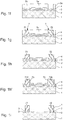
- the substrate 1 used in step a) of the method according to the invention is, for example, formed by a ceramic, sapphire, enamel or other substrate, and having a curved surface.
- a first step a) of the process for example, by a physical vapor phase (PVD) process, a first bond layer 2 and a second conductive layer 3, that is to say a layer capable of start a metallic deposit by galvanic means.
- PVD physical vapor phase
- the tie layer 2 is of the Ti, Ta, Cr or Th type, and has a thickness between 30 nm and 80 nm
- the conductive layer 3 is of the Au, Pt, Ag, Cr, Pd, TiN type, CrN, ZrN, Ni ( figure 1a ) and also has a thickness between 30nm and 80nm.
- the first and second tie layers can be deposited by any other means known to those skilled in the art.
- a third tie layer 4 is deposited, for example by physical vapor deposition with magnetron sputtering, on the second conductive layer 3.
- the tie layer 4 is for example of the SiO type. 2 , TiO 2 , AlN or Si x N y, for example SiN or Si 3 N 4 , and has a thickness of at least 10 nm.
- Such a bonding layer 4 has the particular advantage of allowing optimum adhesion of the resin for the next stage of the coating. process.
- This third bonding layer 4 also makes it possible to form a protective layer on the second conductive layer in the event of detachment of the resin, which prevents unwanted galvanic growth during the subsequent steps of the process.
- the photosensitive resin 5 used in step c) of the process according to the invention is preferably a negative type resin based on octofunctional epoxy available from Microchem under the reference SU-8 and a photoinitiator chosen from salts of triarylsulfonium such as those described in the patent US 4,058,401 .
- This resin is capable of being photopolymerized under the action of UV radiation.
- a solvent which has been found to be suitable for this resin is gammabutyrolactone (GBL).
- a resin based on phenolformaldehyde of the Novolac type in the presence of a DNQ photoinitiator can also be used.
- the resin 5 is deposited on the substrate 1 by any suitable means, by centrifugal coating, with a spinner, or even by spraying to the desired thickness.
- the resin thickness is between 1 ⁇ m and 500 ⁇ m, and more preferably between 20 ⁇ m and 300 ⁇ m. According to the desired thickness and the deposition technique used, the resin 5 will be deposited in one or more times.
- the resin 5 is then heated between 80 and 95 ° C for a period depending on the thickness deposited to remove the solvent. This heating dries and hardens the resin.
- step d) illustrated in figure 1d consists in irradiating the resin layer 5 by means of UV radiation through a mask 6 defining the outline of the desired decorations and thus the photopolymerized zones 5a and the non-photopolymerized zones 5b.
- this UV irradiation is 200 to 1000 mJ.cm-2, measured at a typical wavelength of 365 nm depends on the thickness of the layer and the type of resin selected.
- a step of annealing the resin layer 5 may be necessary to complete the photopolymerization induced by UV irradiation. This annealing step is preferably carried out between 90 ° C and 95 ° C for 15 to 30 minutes.
- the photopolymerized zones 5a become insensitive to a large majority of solvents.
- the non-photopolymerized zones can subsequently be dissolved by a solvent.
- step e) illustrated in figure 1e consists in developing the non-photopolymerized areas 5b of the photosensitive resin layer to show in places the bonding layer 4 of the substrate 1.
- This operation is carried out by dissolving the non-photopolymerized areas 5b by means of a suitable solvent, for example chosen from GBL (gammabutyrolactone) and PGMEA (propylene glycol methyl ethyl acetate).
- a suitable solvent for example chosen from GBL (gammabutyrolactone) and PGMEA (propylene glycol methyl ethyl acetate).
- step f) illustrated in figure 1f consists of eliminating the third tie layer 4 in the mold formed to reveal the second conductive layer 3.
- the third tie layer 4 is removed by plasma etching or reactive ion etching (RIE).
- step g) illustrated in figure 1g consists in galvanically depositing in the molds a layer of a metal from said conductive layer 3 until a plurality of blocks 71, 72 are formed, preferably reaching the height of the molds, the thickness of the metal layer being between 1 ⁇ m and 500 ⁇ m, and more preferably between 20 ⁇ m and 300 ⁇ m.
- metal in this context are of course understood metal alloys.
- the metal will be chosen from the group comprising nickel, copper, gold or silver, and, as an alloy, gold-copper, nickel-cobalt, nickel-iron, nickel-phosphorus or nickel-tungsten.
- the electroforming conditions in particular the composition of the baths, the geometry of the system, the voltages and current densities, are chosen for each metal or alloy to be electrodeposited according to techniques well known in the art of electroforming (cf. example Di Bari GA "electroforming” Electroplating Engineering Handbook 4th Edition written by LJ Durney, published by Van Nostrand Reinhold Compagny Inc., NY USA 1984 ).
- step h) illustrated in figure 1h consists in removing the resin layer 5a from the electrodeposited blocks 71, 72 and from the substrate 1 by means of plasma etching, which makes it possible to remove the resin without damaging the electrodeposited blocks 71, 72.
- a substrate 1 is obtained with electrodeposited blocks 71, 72 forming a decoration on the substrate 1, the first, second and third layers 2, 3, 4 still being present in places, on the substrate after removing the remaining resin.
- the first, second and third layers 2, 3, 4 are removed by means of at least one wet etching.
- SiO 2 or TiO 2 layers are etched with acid hydrofluoric or BOE (buffered oxide etchant).
- the Au layer is etched with aqua regia (nitric acid + hydrochloric acid) or KI (potassium iodide) or KCN (potassium cyanide).
- the nickel is etched with nitric acid.
- the parts obtained can be cleaned, and optionally taken up on a machine tool to perform machining or an aesthetic finish.
- the parts can be used directly or else subjected to various decorative and / or functional treatments, typically physical or chemical deposits.
- step g) a layer of a first metal such as for example nickel is galvanically deposited from said conductive layer to form a block 710, 720 of a height less than or equal up to the resin.
- step h) remains the same, and an additional step h ′) is carried out during which a layer 73 of another metal or alloy, for example precious such as gold, is galvanically deposited on top of the layer. layer of the first metal.
- step i) the tie layer 4 and the conductive 3 and tie 2 layers are removed by at least one wet etching.
- Such an alternative is less expensive and easier to implement, the growth of nickel being easier to control and less expensive than a precious metal such as gold.
- the method of the invention finds a particularly advantageous application for the manufacture of decorative parts for timepieces, and more particularly for domed dials in non-conductive material, having metallic decorations on its surface.
- the decorations can be indexes, appliques, logos or brand names for example. Thanks to this process, it is possible to provide a domed dial in non-conductive material with any type of metallic decoration that perfectly matches the curvature of the surface of the domed dial, with a very precise positioning, and in a multi-part process therefore economically interesting.
Landscapes
- Chemical & Material Sciences (AREA)
- Physics & Mathematics (AREA)
- General Physics & Mathematics (AREA)
- Engineering & Computer Science (AREA)
- Metallurgy (AREA)
- Chemical Kinetics & Catalysis (AREA)
- Electrochemistry (AREA)
- Materials Engineering (AREA)
- Organic Chemistry (AREA)
- Manufacturing & Machinery (AREA)
- Crystallography & Structural Chemistry (AREA)
- Optics & Photonics (AREA)
- Plasma & Fusion (AREA)
- Laminated Bodies (AREA)
- Adornments (AREA)
- Other Surface Treatments For Metallic Materials (AREA)
- Micromachines (AREA)
Description
- La présente invention concerne un procédé de fabrication d'un décor métallique par une technologie de type LIGA. En particulier l'invention concerne un tel procédé pour la fabrication d'un cadran en céramique bombé avec un décor métallique s'adaptant de façon optimale sur le cadran. L'invention concerne également un tel cadran obtenu par ce procédé.
- La technologie LIGA (Lithographie Galvanik Abformung) développée par W. Ehrfeld du Karlsruhe Nuclear Research Center, Allemagne) dans les années 80 s'est révélée intéressante pour la fabrication de microstructures métalliques de haute précision.
- Dans son principe, la technique LIGA consiste à déposer sur un substrat conducteur ou revêtu d'une couche conductrice, une couche d'une résine photosensible, à effectuer à travers un masque correspondant au contour de la microstructure désirée une irradiation X au moyen d'un synchrotron, à développer, c'est-à-dire à éliminer par des moyens physiques ou chimiques les portions de la couche de résine photosensible non irradiées afin de définir un moule ayant le contour de la microstructure, à déposer galvaniquement un métal, typiquement du nickel, dans le moule en résine photosensible, puis à éliminer le moule pour libérer la microstructure.
- La qualité des microstructures obtenues ne prête pas à critique, mais la nécessité de mettre en œuvre un équipement coûteux (synchrotron) rend cette technique peu compatible avec une production de masse de microstructures devant avoir un faible coût unitaire.
- C'est pourquoi sur la base de ce procédé LIGA ont été développés des procédé analogues mais utilisant des résines photosensibles aux UV. Un tel procédé est notamment décrit dans le document
CH 704 955 - se munir d'un substrat dont au moins une des faces est conductrice ;
- appliquer sur la face conductrice du substrat une couche de résine photosensible ;
- irradier la couche de résine à travers un masque définissant le contour de la microstructure désirée ;
- dissoudre les zones non irradiées de la couche de résine photosensible pour faire apparaître par endroit la face conductrice du substrat ;
- déposer galvaniquement des couches alternativement d'un premier métal et d'au moins un deuxième métal à partir de ladite face conductrice pour former un bloc atteignant sensiblement la surface supérieure de la résine photosensible, ledit bloc étant formé d'un empilement de couches des premier et deuxième métaux ;
- séparer par délamination la couche de résine et le bloc électrodéposé du substrat ;
- éliminer la couche de résine photosensible de la structure délaminée pour libérer la microstructure ainsi formée.
- La réalisation de décors métalliques par dépôt galvanique selon ce procédé de l'art antérieur est faite sur une surface plane et sa mise en œuvre sur une pièce présentant surface bombée est bien plus complexe, la courbure de la pièce ne permettant pas de monter correctement les décors.
- On connait également du brevet
EP 2 380 864 et de la publication Sensors and Actuators A: Physical, 168 (1), pp. 105-111, 2011-07-01, Elsevier BV, NL, un élément céramique incrusté d'au moins un décor métallique. - La présente invention a pour but de remédier aux inconvénients susmentionnés ainsi qu'à d'autres encore en fournissant un procédé permettant de fabriquer des décors métalliques se conformant à la courbure des pièces à décorer.
- La présente invention a également pour but de fournir un tel procédé qui soit simple et peu couteux à mettre en œuvre.
- A cet effet l'invention a pour objet un procédé de fabrication d'au moins un décor métallique sur un substrat en matériau isolant présentant une surface bombée comprenant les étapes suivantes :
- a) se munir d'un substrat non conducteur, par exemple en matière céramique, présentant une surface bombée, déposer au moins une première couche d'accroche, et une deuxième couche électriquement conductrice, via un procédé PVD ou équivalent;
- b) déposer une troisième couche d'accroche via un procédé PVD ou équivalent ;
- c) appliquer une couche de résine photosensible ;
- d) irradier la couche de résine à travers un masque définissant la géométrie des décors désirés ;
- e) dissoudre les zones non irradiées de la couche de résine photosensible pour faire apparaître la troisième couche d'accroche à l'emplacement des décors ;
- f) éliminer la troisième couche d'accroche à l'emplacement des décors pour faire apparaitre la deuxième couche électriquement conductrice;
- g) déposer galvaniquement une couche d'un métal à partir de ladite face conductrice pour former un bloc atteignant sensiblement la surface supérieure de la résine photosensible ;
- h) éliminer la couche de résine restante par gravure plasma ;
- i) éliminer les première, deuxième et troisième couches par une gravure humide.
- Ce procédé permet donc la réalisation de pièces terminées en céramique présentant une surface bombée avec des décors métalliques en relief s'adaptant parfaitement à la surface.
- Conformément à d'autres variantes avantageuses de l'invention :
- ladite première couche d'accroche est du type Ti, Ta, Cr ou Th ;
- ladite deuxième couche électriquement conductrice est du type Au, Pt, Ag, Cr, Pd, TiN, CrN, ZrN, Ni ;
- ladite troisième couche d'accroche est du type SiO2, TiO2, AIN ou SixNy;
- la première couche d'accroche présente une épaisseur comprise entre 30nm et 80nm ;
- la deuxième couche conductrice présente une épaisseur comprise entre 30nm et 80nm ;
- la troisième couche d'accroche présente une épaisseur d'au moins 10nm ;
- selon une variante du procédé, durant l'étape g), un premier métal est déposé à hauteur du moule, et avant l'étape i), le procédé comporte une étape h') de dépôt d'un deuxième métal recouvrant le premier métal déposé ;
- le substrat en matériau isolant, est un substrat non conducteur électriquement en céramique, en saphir, en nacre, en verre, en quartz, en diamant, en matière minérale (granit, marbre, ...), en polymères, en composites ou en émail.
- Enfin, l'invention se rapporte à un cadran bombé en matériau isolant présentant des décors métalliques, destiné à être rapporté sur une boîte de montre, et obtenu selon un procédé conforme à l'invention, les décorations étant des index, des appliques, et/ou un logo.
- On comprend donc que le procédé de l'invention trouve une application particulièrement avantageuse pour la fabrication de pièces décoratives pour les pièces d'horlogerie.
- D'autres caractéristiques et avantages de la présente invention ressortiront plus clairement de la description détaillée qui suit d'un exemple de réalisation d'un procédé selon l'invention, cet exemple étant donné seulement à titre purement illustratif et non limitatif, en liaison avec le dessin annexé sur lequel :
- les
figures 1a à 1i illustrent les étapes de procédé d'un mode de réalisation de l'invention en vue de la réalisation d'un cadran muni d'appliques. - Le substrat 1 utilisé dans l'étape a) du procédé selon l'invention est, par exemple, formé par un substrat en céramique, saphir, émail ou autre, et présentant une surface bombée. Lors de la première étape a) du procédé on dépose, par exemple, par procédé physique en phase vapeur (PVD), une première couche d'accroche 2 et une deuxième couche conductrice 3, c'est-à-dire une couche apte à démarrer un dépôt métallique par voie galvanique. Typiquement, la couche d'accroche 2 est du type Ti, Ta, Cr ou Th, et présente une épaisseur comprise entre 30nm et 80 nm, et la couche conductrice 3 est du type Au, Pt, Ag, Cr, Pd, TiN, CrN, ZrN, Ni (
figure 1a ) et présente également une épaisseur comprise entre 30nm et 80 nm. Les première et deuxième couches d'accroche peuvent être déposées par tout autre moyen connu de l'homme du métier. - Lors de l'étape b) une troisième couche d'accroche 4 est déposée, par exemple par dépôt physique en phase vapeur avec pulvérisation cathodique au magnétron, sur la deuxième couche conductrice 3. La couche d'accroche 4 est par exemple du type SiO2, TiO2, AIN ou SixNy par exemple SiN ou Si3N4, et présente une épaisseur d'au moins 10nm.
- Une telle couche d'accroche 4 a notamment pour avantage de permettre une adhérence optimale de la résine pour l'étape suivante du procédé. Cette troisième couche d'accroche 4 permet aussi de former une couche protectrice sur la deuxième couche conductrice en cas de décollement de la résine, ce qui évite une croissance galvanique non désirée lors des étapes ultérieures du procédé.
- La résine photosensible 5 utilisée à l'étape c) du procédé selon l'invention est de préférence une résine de type négative à base d'époxy octofonctionnelle disponible chez Microchem sous la référence SU-8 et d'un photoinitiateur choisi parmi les sels de triarylsulfonium tels que ceux décrits dans le brevet
US 4,058,401 . Cette résine est susceptible d'être photopolymérisée sous l'action d'un rayonnement UV. On notera qu'un solvant qui s'est révélé approprié pour cette résine est le gammabutyrolactone (GBL). - Alternativement, une résine à base de phénolformaldéhyde de type Novolac en présence d'un photoinitiateur DNQ (DiazoNaphtoQuinone) peut également être utilisée.
- La résine 5 est déposée sur le substrat 1 par tout moyen approprié, par enduction centrifuge, à la tournette, ou encore par sprayage jusqu'à l'épaisseur souhaitée. Typiquement l'épaisseur de résine est comprise entre 1 µm et 500 µm, et plus préférentiellement entre 20 µm et 300 µm. Selon l'épaisseur désirée et la technique de dépôt utilisée la résine 5 sera déposée en une ou plusieurs fois.
- La résine 5 est ensuite chauffée entre 80 et 95° C pendant une durée dépendant de l'épaisseur déposée pour évacuer le solvant. Ce chauffage sèche et durcit la résine.
- L'étape d) suivante illustrée à la
figure 1d consiste à irradier la couche de résine 5 au moyen d'un rayonnement UV à travers un masque 6 définissant le contour des décors souhaités et ainsi des zones photopolymérisées 5a et des zones non photopolymérisées 5b. Typiquement, cette irradiation UV est de 200 à 1'000 mJ.cm-2, mesurée à une longueur d'onde typique de 365 nm dépend de l'épaisseur de la couche et du type de résine sélectionnée. - Le cas échéant, une étape de recuit de la couche de résine 5 peut être nécessaire pour compléter la photopolymérisation induite par l'irradiation UV. Cette étape de recuit est effectuée de préférence entre 90°C et 95°C pendant 15 à 30 mn. Les zones photopolymérisées 5a deviennent insensibles à une grande majorité de solvants. Par contre, les zones non photopolymérisées pourront ultérieurement être dissoutes par un solvant.
- L'étape e) suivante illustrée à la
figure 1e consiste à développer les zones non photopolymérisées 5b de la couche de résine photosensible pour faire apparaître par endroit la couche d'accroche 4 du substrat 1. Cette opération est réalisée par dissolution des zones non photopolymérisées 5b au moyen d'un solvant adéquat, par exemple choisi parmi le GBL (gammabutyrolactone) et le PGMEA (propylène glycol méthyle éthyle acétate). Un moule en résine photosensible photopolymérisées 5a présentant les contours d'un décor est ainsi réalisé. - L'étape f) suivante illustrée à la
figure 1f consiste à éliminer la troisième couche d'accroche 4 dans le moule formé pour faire apparaitre la deuxième couche conductrice 3. Typiquement, la troisième couche d'accroche 4 est éliminée au moyen d'une gravure plasma ou d'une gravure ionique réactive (RIE). - L'étape g) suivante illustrée à la
figure 1g consiste à déposer galvaniquement dans les moules une couche d'un métal à partir de ladite couche conductrice 3 jusqu'à former une pluralité de blocs 71, 72, atteignant préférentiellement la hauteur des moules, l'épaisseur de la couche de métal étant comprise entre 1 µm et 500 µm, et plus préférentiellement entre 20 µm et 300 µm. Par métal dans ce contexte sont bien entendu compris les alliages métalliques. Typiquement, le métal sera choisi parmi l'ensemble comprenant le nickel, le cuivre, l'or ou l'argent, et, comme alliage, l'or-cuivre, le nickel-cobalt, le nickel-fer, le nickel-phosphore ou le nickel-tungstène. - Les conditions d'électroformage, notamment la composition des bains, la géométrie du système, les tensions et densités de courant, sont choisis pour chaque métal ou alliage à électrodéposer selon les techniques bien connues dans l'art de l'électroformage (cf. par exemple Di Bari G.A. "electroforming" Electroplating Engineering Handbook 4th Edition rédigée par L.J. Durney, publié par Van Nostrand Reinhold Compagny Inc., N.Y. USA 1984).
- L'étape h) suivante illustrée à la
figure 1h consiste à éliminer la couche de résine 5a des blocs électrodéposés 71, 72 et du substrat 1 au moyen d'une gravure plasma, ce qui permet d'enlever la résine sans endommager les blocs électrodéposés 71, 72. - A l'issue de cette étape h), on obtient un substrat 1 avec des blocs électrodéposés 71, 72 formant un décor sur le substrat 1, les première, deuxième et troisième couches 2, 3, 4 étant encore présentes par endroit, sur le substrat après l'élimination de la résine restante.
- A l'étape i) illustrée à la
figure 1i , les première, deuxième et troisième couches 2, 3, 4 sont éliminées au moyen d'au moins une gravure humide. Par exemple, les couches SiO2 ou TiO2 sont gravées avec de l'acide fluorhydrique ou BOE (buffered oxide etchant). La couche Au est gravée avec de l'eau régale (acide nitrique + acide chlorhydrique) ou du KI (iodure de potassium) ou KCN (cyanure de potassium). Le nickel est gravé avec de l'acide nitrique. - A l'issue de cette étape, les pièces obtenues peuvent être nettoyées, et éventuellement reprises sur une machine-outil pour opérer des usinages ou une terminaison esthétique. A ce stade, les pièces peuvent être directement utilisées ou bien soumises à divers traitements décoratifs et/ou fonctionnels, typiquement des dépôts physiques ou chimiques.
- Selon une alternative de l'invention, à l'étape g) on dépose galvaniquement une couche d'un premier métal tel que par exemple du nickel à partir de ladite couche conductrice pour former un bloc 710, 720 d'une hauteur inférieure ou égale à la hauteur de la résine. L'étape suivante h) reste la même, et une étape additionnelle h') est effectuée au cours de laquelle on dépose galvaniquement une couche 73 d'un autre métal ou alliage, par exemple précieux tel que de l'or par-dessus la couche du premier métal. Enfin, à l'étape i) la couche d'accroche 4 et les couches conductrice 3 et d'accroche 2 sont éliminées par au moins une gravure humide.
- Une telle alternative est moins couteuse et plus facile à mettre en œuvre, la croissance du nickel étant plus facile à maitriser et moins couteuse qu'un métal précieux tel que l'or.
- Le procédé de l'invention trouve une application particulièrement avantageuse pour la fabrication de pièces décoratives pour pièces d'horlogerie, et plus particulièrement pour des cadrans bombés en matière non conductrice, présentant des décorations métalliques à sa surface. Les décorations peuvent être des index, des appliques, des logos ou des noms de marque par exemple. Grâce à ce procédé, on peut munir un cadran bombé en matière non conductrice de tout type de décoration métallique s'adaptant parfaitement à la courbure de la surface du cadran bombé, avec un positionnement très précis, et en procédé multi-pièces donc économiquement intéressant.
Claims (9)
- Procédé de fabrication d'au moins un décor métallique sur un substrat (1) en matériau isolant présentant une surface bombée comprenant les étapes suivantes :a) se munir du substrat (1) et y déposer une première couche (2) d'accroche et une deuxième couche (3) électriquement conductrice via un dépôt en phase vapeur ;b) déposer une troisième couche (4) d'accroche,c) appliquer une couche (5) de résine photosensible ;d) irradier la couche (5) de résine à travers un masque (6) définissant le contour des décors désirés ;e) dissoudre les zones (5b) non irradiées de la couche de résine photosensible (5) pour faire apparaître par endroit la troisième couche d'accroche (4) à l'emplacement des décors ;f) éliminer la troisième couche d'accroche (4) à l'emplacement des décors pour faire apparaitre la deuxième couche conductrice (3) ;g) déposer galvaniquement une couche d'un métal (7) ou d'un alliage métallique à partir de ladite face conductrice pour former au moins un bloc (71, 72) atteignant sensiblement la surface supérieure de la résine photosensible (5) ;h) éliminer la couche de résine (5) restante par gravure plasma ;i) éliminer les première, deuxième et troisième couches par au moins une gravure humide.
- Procédé selon la revendication 1, caractérisé en ce que ladite première couche d'accroche est du type Ti, Ta, Cr ou Th.
- Procédé selon la revendication 1 ou 2, caractérisé en ce que ladite deuxième couche électriquement conductrice est du type Au, Pt, Ag, Cr, Pd, TiN, CrN, ZrN, Ni.
- Procédé selon l'une quelconques des revendications 1 à 3, caractérisé en ce que ladite troisième couche d'accroche est du type SiO2, TiO2, AIN ou SixNy TiO2,
- Procédé selon l'une des revendications précédentes, caractérisé en ce que la première couche d'accroche (2) présente une épaisseur comprise entre 30nm et 80nm.
- Procédé selon l'une des revendications précédentes, caractérisé en ce que la deuxième couche conductrice (3) présente une épaisseur comprise entre 30nm et 80nm.
- Procédé selon l'une des revendications précédentes, caractérisé en ce que la troisième couche d'accroche (4) présente une épaisseur d'au moins 10nm.
- Procédé selon l'une des revendications précédentes, caractérisé en ce que :- durant l'étape g), un premier métal est déposé à hauteur du moule ;- avant l'étape i), le procédé comporte une étape h') de dépôt d'un deuxième métal ou alliage métallique recouvrant le premier métal déposé.
- Procédé selon l'une des revendications précédentes, caractérisé en ce que le substrat (1) en matériau isolant, est un substrat en céramique, en saphir, en nacre, en verre, en quartz, en diamant, en matière minérale , en polymères, en composites, en verre ou en émail.
Priority Applications (5)
| Application Number | Priority Date | Filing Date | Title |
|---|---|---|---|
| EP18161026.2A EP3536826B1 (fr) | 2018-03-09 | 2018-03-09 | Procede de fabrication d'un decor metallique sur un cadran et cadran obtenu selon ce procede |
| CH00295/18A CH714739A2 (fr) | 2018-03-09 | 2018-03-09 | Procédé de fabrication d’un décor métallique sur un cadran et cadran obtenu selon ce procédé. |
| JP2019019526A JP6861231B2 (ja) | 2018-03-09 | 2019-02-06 | 表盤上に金属装飾を製造する方法及びこの方法によって得られる表盤 |
| US16/271,912 US12072632B2 (en) | 2018-03-09 | 2019-02-11 | Method for fabricating a metal decoration on a dial and dial obtained by this method |
| CN201910150206.5A CN110244543B (zh) | 2018-03-09 | 2019-02-28 | 在表盘上制造金属装饰物的方法及由该方法获得的表盘 |
Applications Claiming Priority (1)
| Application Number | Priority Date | Filing Date | Title |
|---|---|---|---|
| EP18161026.2A EP3536826B1 (fr) | 2018-03-09 | 2018-03-09 | Procede de fabrication d'un decor metallique sur un cadran et cadran obtenu selon ce procede |
Publications (2)
| Publication Number | Publication Date |
|---|---|
| EP3536826A1 EP3536826A1 (fr) | 2019-09-11 |
| EP3536826B1 true EP3536826B1 (fr) | 2021-04-28 |
Family
ID=61622381
Family Applications (1)
| Application Number | Title | Priority Date | Filing Date |
|---|---|---|---|
| EP18161026.2A Active EP3536826B1 (fr) | 2018-03-09 | 2018-03-09 | Procede de fabrication d'un decor metallique sur un cadran et cadran obtenu selon ce procede |
Country Status (5)
| Country | Link |
|---|---|
| US (1) | US12072632B2 (fr) |
| EP (1) | EP3536826B1 (fr) |
| JP (1) | JP6861231B2 (fr) |
| CN (1) | CN110244543B (fr) |
| CH (1) | CH714739A2 (fr) |
Cited By (2)
| Publication number | Priority date | Publication date | Assignee | Title |
|---|---|---|---|---|
| EP4485088A1 (fr) * | 2023-06-28 | 2025-01-01 | Richemont International S.A. | Procédé de retrait d'un matériau céramique |
| EP4512273A1 (fr) * | 2023-08-23 | 2025-02-26 | Comadur S.A. | Procédé de décoration en trois dimensions d'un substrat afin de réaliser une pièce d'habillage |
Families Citing this family (9)
| Publication number | Priority date | Publication date | Assignee | Title |
|---|---|---|---|---|
| JP7015481B2 (ja) * | 2019-11-07 | 2022-02-03 | カシオ計算機株式会社 | 文字板および時計 |
| EP3839659B1 (fr) * | 2019-12-16 | 2024-04-03 | Rubattel et Weyermann S.A. | Procédé de décoration d'une pièce mécanique |
| EP3839626B1 (fr) * | 2019-12-18 | 2023-10-11 | Nivarox-FAR S.A. | Procede de fabrication d'un composant horloger |
| EP3926413A1 (fr) * | 2020-06-17 | 2021-12-22 | Rubattel et Weyermann S.A. | Formation d'un objet tridimensionnel sur un cadran |
| EP3951512B1 (fr) * | 2020-08-04 | 2023-03-01 | Comadur S.A. | Procede de fabrication d'une piece comprenant au moins un motif metallise en trois dimensions |
| EP4206826B1 (fr) * | 2021-12-30 | 2026-04-29 | Rubattel et Weyermann S.A. | Procédé de fabrication d'appliques sur un cadran |
| EP4350437A1 (fr) * | 2022-10-07 | 2024-04-10 | Richemont International S.A. | Procédé de fabrication d'un moule pour la formation de pièces métalliques par croissance métallique |
| EP4513276B1 (fr) * | 2023-08-23 | 2026-03-25 | Comadur S.A. | Procédé de décoration en trois dimensions d'un substrat afin de réaliser une pièce d'habillage |
| EP4659621A1 (fr) * | 2024-06-05 | 2025-12-10 | Comadur S.A. | Article avec un décor 3d et son procédé de fabrication |
Family Cites Families (15)
| Publication number | Priority date | Publication date | Assignee | Title |
|---|---|---|---|---|
| US4058401A (en) | 1974-05-02 | 1977-11-15 | General Electric Company | Photocurable compositions containing group via aromatic onium salts |
| JPS55141569A (en) * | 1979-04-24 | 1980-11-05 | Kawaguchiko Seimitsu Kk | Manufacture of dial plate of watch |
| CN100422386C (zh) | 2002-01-16 | 2008-10-01 | 精工爱普生株式会社 | 装饰品的表面处理方法、装饰品和钟表 |
| KR100481180B1 (ko) * | 2002-09-10 | 2005-04-07 | 삼성전자주식회사 | 포토레지스트 제거방법 |
| JP2004327616A (ja) * | 2003-04-23 | 2004-11-18 | Sumitomo Electric Ind Ltd | 金属パターンを形成する方法 |
| JP2005023380A (ja) * | 2003-07-03 | 2005-01-27 | Nikon Corp | 電鋳品製造方法 |
| EP1548525B2 (fr) * | 2003-12-23 | 2017-08-16 | Rolex Sa | Elément en céramique pour boîte de montre et procédé de fabrication de cet élément |
| CH704955B1 (fr) | 2007-12-31 | 2012-11-30 | Nivarox Sa | Procédé de fabrication d'une microstructure métallique et microstructure obtenue selon ce prodédé. |
| CH704572B1 (fr) | 2007-12-31 | 2012-09-14 | Nivarox Sa | Procédé de fabrication d'une microstructure métallique et microstructure obtenue selon ce procédé. |
| JP2010101712A (ja) * | 2008-10-22 | 2010-05-06 | Seiko Epson Corp | 時計用文字板および時計 |
| EP2179952B1 (fr) * | 2008-10-24 | 2018-07-18 | Müller Martini Holding AG | Procédé pour l'union adhésive de deux produits plats, notamment de produits d'impression à l'aide d'un produit d'impression alimenté supplémentaire ou analogue |
| EP2263972A1 (fr) * | 2009-06-12 | 2010-12-22 | Nivarox-FAR S.A. | Procédé de fabrication d'une microstructure métallique et microstructure obtenue selon ce procédé |
| EP2383244A1 (fr) | 2010-04-23 | 2011-11-02 | Omega SA | Elément céramique incrusté d'au moins un décor métallique |
| EP2816142A1 (fr) * | 2013-06-17 | 2014-12-24 | Hochschule Furtwangen | Procédé de production d'une structure de couche poreuse, produit obtenu et utilisation de ce produit |
| EP3035129B1 (fr) | 2014-12-19 | 2020-11-04 | The Swatch Group Research and Development Ltd | Procede de realisation d'un element decore d'une piece d'horlogerie ou de bijouterie |
-
2018
- 2018-03-09 CH CH00295/18A patent/CH714739A2/fr not_active Application Discontinuation
- 2018-03-09 EP EP18161026.2A patent/EP3536826B1/fr active Active
-
2019
- 2019-02-06 JP JP2019019526A patent/JP6861231B2/ja active Active
- 2019-02-11 US US16/271,912 patent/US12072632B2/en active Active
- 2019-02-28 CN CN201910150206.5A patent/CN110244543B/zh active Active
Non-Patent Citations (1)
| Title |
|---|
| None * |
Cited By (4)
| Publication number | Priority date | Publication date | Assignee | Title |
|---|---|---|---|---|
| EP4485088A1 (fr) * | 2023-06-28 | 2025-01-01 | Richemont International S.A. | Procédé de retrait d'un matériau céramique |
| CH720899A1 (fr) * | 2023-06-28 | 2025-01-15 | Richemont Int Sa | Procédé de retrait d'une couche de matériau céramique |
| EP4512273A1 (fr) * | 2023-08-23 | 2025-02-26 | Comadur S.A. | Procédé de décoration en trois dimensions d'un substrat afin de réaliser une pièce d'habillage |
| US12540103B2 (en) | 2023-08-23 | 2026-02-03 | Comadur Sa | Method for the three-dimensional decoration of a substrate to produce an external part |
Also Published As
| Publication number | Publication date |
|---|---|
| CH714739A2 (fr) | 2019-09-13 |
| JP2019157268A (ja) | 2019-09-19 |
| CN110244543B (zh) | 2022-03-25 |
| CN110244543A (zh) | 2019-09-17 |
| US20190278182A1 (en) | 2019-09-12 |
| EP3536826A1 (fr) | 2019-09-11 |
| JP6861231B2 (ja) | 2021-04-21 |
| US12072632B2 (en) | 2024-08-27 |
Similar Documents
| Publication | Publication Date | Title |
|---|---|---|
| EP3536826A1 (fr) | Procede de fabrication d'un decor metallique sur un cadran et cadran obtenu selon ce procede | |
| EP2229470B1 (fr) | Procédé de fabrication d'une microstructure métallique et microstructure obtenue selon ce procédé | |
| EP2440690B1 (fr) | Procede de fabrication d'une microstructure metallique | |
| EP2347036B1 (fr) | Procédé liga hétérogène | |
| EP3839624B1 (fr) | Procede de fabrication d'un composant horloger | |
| WO2009083487A2 (fr) | Procédé de fabrication d'une microstructure métallique et microstructure obtenue selon ce procédé | |
| EP3839626B1 (fr) | Procede de fabrication d'un composant horloger | |
| EP3839659B1 (fr) | Procédé de décoration d'une pièce mécanique | |
| EP3802920B1 (fr) | Procede de fabrication d'un decor metallique sur un cadran et cadran obtenu selon ce procede | |
| EP3951512A1 (fr) | Procede de fabrication d'une piece comprenant au moins un motif metallise en trois dimensions | |
| EP3839625A1 (fr) | Procede de fabrication d'un composant horloger et composant obtenu selon ce procede | |
| EP3467151A1 (fr) | Moule pour galvanoplastie et son procédé de fabrication | |
| CH716967A2 (fr) | Procédé de fabrication d'un composant horloger et composant obtenu selon ce procédé. | |
| CH715028A2 (fr) | Procédé de fabrication d'un décor métallique sur un substrat et cadran obtenu par un tel procédé. | |
| EP3841433B1 (fr) | Procede de fabrication d'un composant horloger et composant obtenu selon ce procede | |
| EP4575045A1 (fr) | Procédé de fabrication de composants horlogers en lot | |
| CH715266A2 (fr) | Procédé de fabrication d'un composant horloger et composant obtenu selon ce procédé. | |
| CH721414A2 (fr) | Procédé de fabrication de composants horlogers en lot | |
| HK40014352B (zh) | 在表盘上制造金属装饰物的方法及由该方法获得的表盘 | |
| HK40014352A (en) | Method for fabricating a metal decoration on a dial and dial obtained by this method | |
| EP2833204A1 (fr) | Procede de traitement d'une couche de resine photosensible et procede de fabrication d'un composant metallique | |
| CH716969A2 (fr) | Procédé de fabrication d'un composant horloger et composant obtenu selon ce procédé. | |
| HK40043290A (en) | Method for producing a metal decorative element on a watch dial, and watch dial obtained using this method | |
| CH716966A2 (fr) | Procédé de fabrication d'un composant horloger et composant obtenu selon ce procédé. | |
| HK40043290B (en) | Method for producing a metal decorative element on a watch dial, and watch dial obtained using this method |
Legal Events
| Date | Code | Title | Description |
|---|---|---|---|
| PUAI | Public reference made under article 153(3) epc to a published international application that has entered the european phase |
Free format text: ORIGINAL CODE: 0009012 |
|
| STAA | Information on the status of an ep patent application or granted ep patent |
Free format text: STATUS: THE APPLICATION HAS BEEN PUBLISHED |
|
| AK | Designated contracting states |
Kind code of ref document: A1 Designated state(s): AL AT BE BG CH CY CZ DE DK EE ES FI FR GB GR HR HU IE IS IT LI LT LU LV MC MK MT NL NO PL PT RO RS SE SI SK SM TR |
|
| AX | Request for extension of the european patent |
Extension state: BA ME |
|
| STAA | Information on the status of an ep patent application or granted ep patent |
Free format text: STATUS: REQUEST FOR EXAMINATION WAS MADE |
|
| 17P | Request for examination filed |
Effective date: 20200311 |
|
| RBV | Designated contracting states (corrected) |
Designated state(s): AL AT BE BG CH CY CZ DE DK EE ES FI FR GB GR HR HU IE IS IT LI LT LU LV MC MK MT NL NO PL PT RO RS SE SI SK SM TR |
|
| REG | Reference to a national code |
Ref country code: DE Ref legal event code: R079 Ref document number: 602018016053 Country of ref document: DE Free format text: PREVIOUS MAIN CLASS: C25D0007000000 Ipc: C25D0005020000 |
|
| RIC1 | Information provided on ipc code assigned before grant |
Ipc: G03F 7/00 20060101ALN20200901BHEP Ipc: G04B 19/10 20060101ALI20200901BHEP Ipc: G03F 7/18 20060101ALN20200901BHEP Ipc: G04B 19/12 20060101ALI20200901BHEP Ipc: C25D 5/02 20060101AFI20200901BHEP Ipc: C25D 1/00 20060101ALI20200901BHEP Ipc: G04B 45/00 20060101ALI20200901BHEP Ipc: C25D 7/00 20060101ALI20200901BHEP Ipc: G04B 37/22 20060101ALI20200901BHEP |
|
| GRAP | Despatch of communication of intention to grant a patent |
Free format text: ORIGINAL CODE: EPIDOSNIGR1 |
|
| RIC1 | Information provided on ipc code assigned before grant |
Ipc: G03F 7/18 20060101ALN20200921BHEP Ipc: G04B 37/22 20060101ALI20200921BHEP Ipc: C25D 1/00 20060101ALI20200921BHEP Ipc: G04B 19/12 20060101ALI20200921BHEP Ipc: C25D 5/02 20060101AFI20200921BHEP Ipc: C25D 7/00 20060101ALI20200921BHEP Ipc: G04B 19/10 20060101ALI20200921BHEP Ipc: G03F 7/00 20060101ALN20200921BHEP Ipc: G04B 45/00 20060101ALI20200921BHEP |
|
| STAA | Information on the status of an ep patent application or granted ep patent |
Free format text: STATUS: GRANT OF PATENT IS INTENDED |
|
| INTG | Intention to grant announced |
Effective date: 20201029 |
|
| GRAS | Grant fee paid |
Free format text: ORIGINAL CODE: EPIDOSNIGR3 |
|
| GRAA | (expected) grant |
Free format text: ORIGINAL CODE: 0009210 |
|
| STAA | Information on the status of an ep patent application or granted ep patent |
Free format text: STATUS: THE PATENT HAS BEEN GRANTED |
|
| AK | Designated contracting states |
Kind code of ref document: B1 Designated state(s): AL AT BE BG CH CY CZ DE DK EE ES FI FR GB GR HR HU IE IS IT LI LT LU LV MC MK MT NL NO PL PT RO RS SE SI SK SM TR |
|
| REG | Reference to a national code |
Ref country code: GB Ref legal event code: FG4D Free format text: NOT ENGLISH |
|
| REG | Reference to a national code |
Ref country code: CH Ref legal event code: EP |
|
| REG | Reference to a national code |
Ref country code: AT Ref legal event code: REF Ref document number: 1387134 Country of ref document: AT Kind code of ref document: T Effective date: 20210515 |
|
| REG | Reference to a national code |
Ref country code: DE Ref legal event code: R096 Ref document number: 602018016053 Country of ref document: DE |
|
| REG | Reference to a national code |
Ref country code: IE Ref legal event code: FG4D Free format text: LANGUAGE OF EP DOCUMENT: FRENCH |
|
| REG | Reference to a national code |
Ref country code: LT Ref legal event code: MG9D |
|
| REG | Reference to a national code |
Ref country code: AT Ref legal event code: MK05 Ref document number: 1387134 Country of ref document: AT Kind code of ref document: T Effective date: 20210428 |
|
| PG25 | Lapsed in a contracting state [announced via postgrant information from national office to epo] |
Ref country code: NL Free format text: LAPSE BECAUSE OF FAILURE TO SUBMIT A TRANSLATION OF THE DESCRIPTION OR TO PAY THE FEE WITHIN THE PRESCRIBED TIME-LIMIT Effective date: 20210428 Ref country code: BG Free format text: LAPSE BECAUSE OF FAILURE TO SUBMIT A TRANSLATION OF THE DESCRIPTION OR TO PAY THE FEE WITHIN THE PRESCRIBED TIME-LIMIT Effective date: 20210728 Ref country code: AT Free format text: LAPSE BECAUSE OF FAILURE TO SUBMIT A TRANSLATION OF THE DESCRIPTION OR TO PAY THE FEE WITHIN THE PRESCRIBED TIME-LIMIT Effective date: 20210428 Ref country code: HR Free format text: LAPSE BECAUSE OF FAILURE TO SUBMIT A TRANSLATION OF THE DESCRIPTION OR TO PAY THE FEE WITHIN THE PRESCRIBED TIME-LIMIT Effective date: 20210428 Ref country code: LT Free format text: LAPSE BECAUSE OF FAILURE TO SUBMIT A TRANSLATION OF THE DESCRIPTION OR TO PAY THE FEE WITHIN THE PRESCRIBED TIME-LIMIT Effective date: 20210428 Ref country code: FI Free format text: LAPSE BECAUSE OF FAILURE TO SUBMIT A TRANSLATION OF THE DESCRIPTION OR TO PAY THE FEE WITHIN THE PRESCRIBED TIME-LIMIT Effective date: 20210428 |
|
| PG25 | Lapsed in a contracting state [announced via postgrant information from national office to epo] |
Ref country code: NO Free format text: LAPSE BECAUSE OF FAILURE TO SUBMIT A TRANSLATION OF THE DESCRIPTION OR TO PAY THE FEE WITHIN THE PRESCRIBED TIME-LIMIT Effective date: 20210728 Ref country code: LV Free format text: LAPSE BECAUSE OF FAILURE TO SUBMIT A TRANSLATION OF THE DESCRIPTION OR TO PAY THE FEE WITHIN THE PRESCRIBED TIME-LIMIT Effective date: 20210428 Ref country code: PL Free format text: LAPSE BECAUSE OF FAILURE TO SUBMIT A TRANSLATION OF THE DESCRIPTION OR TO PAY THE FEE WITHIN THE PRESCRIBED TIME-LIMIT Effective date: 20210428 Ref country code: PT Free format text: LAPSE BECAUSE OF FAILURE TO SUBMIT A TRANSLATION OF THE DESCRIPTION OR TO PAY THE FEE WITHIN THE PRESCRIBED TIME-LIMIT Effective date: 20210830 Ref country code: RS Free format text: LAPSE BECAUSE OF FAILURE TO SUBMIT A TRANSLATION OF THE DESCRIPTION OR TO PAY THE FEE WITHIN THE PRESCRIBED TIME-LIMIT Effective date: 20210428 Ref country code: SE Free format text: LAPSE BECAUSE OF FAILURE TO SUBMIT A TRANSLATION OF THE DESCRIPTION OR TO PAY THE FEE WITHIN THE PRESCRIBED TIME-LIMIT Effective date: 20210428 Ref country code: IS Free format text: LAPSE BECAUSE OF FAILURE TO SUBMIT A TRANSLATION OF THE DESCRIPTION OR TO PAY THE FEE WITHIN THE PRESCRIBED TIME-LIMIT Effective date: 20210828 Ref country code: GR Free format text: LAPSE BECAUSE OF FAILURE TO SUBMIT A TRANSLATION OF THE DESCRIPTION OR TO PAY THE FEE WITHIN THE PRESCRIBED TIME-LIMIT Effective date: 20210729 |
|
| REG | Reference to a national code |
Ref country code: NL Ref legal event code: MP Effective date: 20210428 |
|
| PG25 | Lapsed in a contracting state [announced via postgrant information from national office to epo] |
Ref country code: SK Free format text: LAPSE BECAUSE OF FAILURE TO SUBMIT A TRANSLATION OF THE DESCRIPTION OR TO PAY THE FEE WITHIN THE PRESCRIBED TIME-LIMIT Effective date: 20210428 Ref country code: SM Free format text: LAPSE BECAUSE OF FAILURE TO SUBMIT A TRANSLATION OF THE DESCRIPTION OR TO PAY THE FEE WITHIN THE PRESCRIBED TIME-LIMIT Effective date: 20210428 Ref country code: ES Free format text: LAPSE BECAUSE OF FAILURE TO SUBMIT A TRANSLATION OF THE DESCRIPTION OR TO PAY THE FEE WITHIN THE PRESCRIBED TIME-LIMIT Effective date: 20210428 Ref country code: EE Free format text: LAPSE BECAUSE OF FAILURE TO SUBMIT A TRANSLATION OF THE DESCRIPTION OR TO PAY THE FEE WITHIN THE PRESCRIBED TIME-LIMIT Effective date: 20210428 Ref country code: RO Free format text: LAPSE BECAUSE OF FAILURE TO SUBMIT A TRANSLATION OF THE DESCRIPTION OR TO PAY THE FEE WITHIN THE PRESCRIBED TIME-LIMIT Effective date: 20210428 Ref country code: DK Free format text: LAPSE BECAUSE OF FAILURE TO SUBMIT A TRANSLATION OF THE DESCRIPTION OR TO PAY THE FEE WITHIN THE PRESCRIBED TIME-LIMIT Effective date: 20210428 Ref country code: CZ Free format text: LAPSE BECAUSE OF FAILURE TO SUBMIT A TRANSLATION OF THE DESCRIPTION OR TO PAY THE FEE WITHIN THE PRESCRIBED TIME-LIMIT Effective date: 20210428 |
|
| REG | Reference to a national code |
Ref country code: DE Ref legal event code: R097 Ref document number: 602018016053 Country of ref document: DE |
|
| PLBE | No opposition filed within time limit |
Free format text: ORIGINAL CODE: 0009261 |
|
| STAA | Information on the status of an ep patent application or granted ep patent |
Free format text: STATUS: NO OPPOSITION FILED WITHIN TIME LIMIT |
|
| 26N | No opposition filed |
Effective date: 20220131 |
|
| PG25 | Lapsed in a contracting state [announced via postgrant information from national office to epo] |
Ref country code: IS Free format text: LAPSE BECAUSE OF FAILURE TO SUBMIT A TRANSLATION OF THE DESCRIPTION OR TO PAY THE FEE WITHIN THE PRESCRIBED TIME-LIMIT Effective date: 20210828 Ref country code: AL Free format text: LAPSE BECAUSE OF FAILURE TO SUBMIT A TRANSLATION OF THE DESCRIPTION OR TO PAY THE FEE WITHIN THE PRESCRIBED TIME-LIMIT Effective date: 20210428 |
|
| PG25 | Lapsed in a contracting state [announced via postgrant information from national office to epo] |
Ref country code: IT Free format text: LAPSE BECAUSE OF FAILURE TO SUBMIT A TRANSLATION OF THE DESCRIPTION OR TO PAY THE FEE WITHIN THE PRESCRIBED TIME-LIMIT Effective date: 20210428 |
|
| PG25 | Lapsed in a contracting state [announced via postgrant information from national office to epo] |
Ref country code: MC Free format text: LAPSE BECAUSE OF FAILURE TO SUBMIT A TRANSLATION OF THE DESCRIPTION OR TO PAY THE FEE WITHIN THE PRESCRIBED TIME-LIMIT Effective date: 20210428 |
|
| GBPC | Gb: european patent ceased through non-payment of renewal fee |
Effective date: 20220309 |
|
| REG | Reference to a national code |
Ref country code: BE Ref legal event code: MM Effective date: 20220331 |
|
| PG25 | Lapsed in a contracting state [announced via postgrant information from national office to epo] |
Ref country code: LU Free format text: LAPSE BECAUSE OF NON-PAYMENT OF DUE FEES Effective date: 20220309 Ref country code: IE Free format text: LAPSE BECAUSE OF NON-PAYMENT OF DUE FEES Effective date: 20220309 Ref country code: GB Free format text: LAPSE BECAUSE OF NON-PAYMENT OF DUE FEES Effective date: 20220309 |
|
| PG25 | Lapsed in a contracting state [announced via postgrant information from national office to epo] |
Ref country code: BE Free format text: LAPSE BECAUSE OF NON-PAYMENT OF DUE FEES Effective date: 20220331 |
|
| P01 | Opt-out of the competence of the unified patent court (upc) registered |
Effective date: 20230615 |
|
| PG25 | Lapsed in a contracting state [announced via postgrant information from national office to epo] |
Ref country code: MK Free format text: LAPSE BECAUSE OF FAILURE TO SUBMIT A TRANSLATION OF THE DESCRIPTION OR TO PAY THE FEE WITHIN THE PRESCRIBED TIME-LIMIT Effective date: 20210428 Ref country code: CY Free format text: LAPSE BECAUSE OF FAILURE TO SUBMIT A TRANSLATION OF THE DESCRIPTION OR TO PAY THE FEE WITHIN THE PRESCRIBED TIME-LIMIT Effective date: 20210428 |
|
| PG25 | Lapsed in a contracting state [announced via postgrant information from national office to epo] |
Ref country code: HU Free format text: LAPSE BECAUSE OF FAILURE TO SUBMIT A TRANSLATION OF THE DESCRIPTION OR TO PAY THE FEE WITHIN THE PRESCRIBED TIME-LIMIT; INVALID AB INITIO Effective date: 20180309 |
|
| PG25 | Lapsed in a contracting state [announced via postgrant information from national office to epo] |
Ref country code: MT Free format text: LAPSE BECAUSE OF FAILURE TO SUBMIT A TRANSLATION OF THE DESCRIPTION OR TO PAY THE FEE WITHIN THE PRESCRIBED TIME-LIMIT Effective date: 20210428 |
|
| PGFP | Annual fee paid to national office [announced via postgrant information from national office to epo] |
Ref country code: CH Payment date: 20250401 Year of fee payment: 8 |
|
| PG25 | Lapsed in a contracting state [announced via postgrant information from national office to epo] |
Ref country code: TR Free format text: LAPSE BECAUSE OF FAILURE TO SUBMIT A TRANSLATION OF THE DESCRIPTION OR TO PAY THE FEE WITHIN THE PRESCRIBED TIME-LIMIT Effective date: 20210428 |
|
| REG | Reference to a national code |
Ref country code: CH Ref legal event code: U11 Free format text: ST27 STATUS EVENT CODE: U-0-0-U10-U11 (AS PROVIDED BY THE NATIONAL OFFICE) Effective date: 20260401 |
|
| PGFP | Annual fee paid to national office [announced via postgrant information from national office to epo] |
Ref country code: DE Payment date: 20260219 Year of fee payment: 9 |
|
| PGFP | Annual fee paid to national office [announced via postgrant information from national office to epo] |
Ref country code: FR Payment date: 20260219 Year of fee payment: 9 |