EP3536660A1 - Selbstausgerichtete nanopore auf rippe - Google Patents
Selbstausgerichtete nanopore auf rippe Download PDFInfo
- Publication number
- EP3536660A1 EP3536660A1 EP18159987.9A EP18159987A EP3536660A1 EP 3536660 A1 EP3536660 A1 EP 3536660A1 EP 18159987 A EP18159987 A EP 18159987A EP 3536660 A1 EP3536660 A1 EP 3536660A1
- Authority
- EP
- European Patent Office
- Prior art keywords
- fin
- nanopore
- pillar
- silicon
- mask
- Prior art date
- Legal status (The legal status is an assumption and is not a legal conclusion. Google has not performed a legal analysis and makes no representation as to the accuracy of the status listed.)
- Withdrawn
Links
Images



Classifications
-
- B—PERFORMING OPERATIONS; TRANSPORTING
- B81—MICROSTRUCTURAL TECHNOLOGY
- B81C—PROCESSES OR APPARATUS SPECIALLY ADAPTED FOR THE MANUFACTURE OR TREATMENT OF MICROSTRUCTURAL DEVICES OR SYSTEMS
- B81C1/00—Manufacture or treatment of devices or systems in or on a substrate
- B81C1/00015—Manufacture or treatment of devices or systems in or on a substrate for manufacturing microsystems
- B81C1/00023—Manufacture or treatment of devices or systems in or on a substrate for manufacturing microsystems without movable or flexible elements
- B81C1/00087—Holes
-
- G—PHYSICS
- G01—MEASURING; TESTING
- G01N—INVESTIGATING OR ANALYSING MATERIALS BY DETERMINING THEIR CHEMICAL OR PHYSICAL PROPERTIES
- G01N27/00—Investigating or analysing materials by the use of electric, electrochemical, or magnetic means
- G01N27/26—Investigating or analysing materials by the use of electric, electrochemical, or magnetic means by investigating electrochemical variables; by using electrolysis or electrophoresis
- G01N27/403—Cells and electrode assemblies
- G01N27/414—Ion-sensitive or chemical field-effect transistors, i.e. ISFETS or CHEMFETS
- G01N27/4145—Ion-sensitive or chemical field-effect transistors, i.e. ISFETS or CHEMFETS specially adapted for biomolecules, e.g. gate electrode with immobilised receptors
-
- C—CHEMISTRY; METALLURGY
- C12—BIOCHEMISTRY; BEER; SPIRITS; WINE; VINEGAR; MICROBIOLOGY; ENZYMOLOGY; MUTATION OR GENETIC ENGINEERING
- C12Q—MEASURING OR TESTING PROCESSES INVOLVING ENZYMES, NUCLEIC ACIDS OR MICROORGANISMS; COMPOSITIONS OR TEST PAPERS THEREFOR; PROCESSES OF PREPARING SUCH COMPOSITIONS; CONDITION-RESPONSIVE CONTROL IN MICROBIOLOGICAL OR ENZYMOLOGICAL PROCESSES
- C12Q1/00—Measuring or testing processes involving enzymes, nucleic acids or microorganisms; Compositions therefor; Processes of preparing such compositions
- C12Q1/68—Measuring or testing processes involving enzymes, nucleic acids or microorganisms; Compositions therefor; Processes of preparing such compositions involving nucleic acids
- C12Q1/6869—Methods for sequencing
-
- G—PHYSICS
- G01—MEASURING; TESTING
- G01N—INVESTIGATING OR ANALYSING MATERIALS BY DETERMINING THEIR CHEMICAL OR PHYSICAL PROPERTIES
- G01N33/00—Investigating or analysing materials by specific methods not covered by groups G01N1/00 - G01N31/00
- G01N33/48—Biological material, e.g. blood, urine; Haemocytometers
- G01N33/483—Physical analysis of biological material
- G01N33/487—Physical analysis of biological material of liquid biological material
- G01N33/48707—Physical analysis of biological material of liquid biological material by electrical means
- G01N33/48721—Investigating individual macromolecules, e.g. by translocation through nanopores
-
- H—ELECTRICITY
- H10—SEMICONDUCTOR DEVICES; ELECTRIC SOLID-STATE DEVICES NOT OTHERWISE PROVIDED FOR
- H10D—INORGANIC ELECTRIC SEMICONDUCTOR DEVICES
- H10D30/00—Field-effect transistors [FET]
- H10D30/01—Manufacture or treatment
- H10D30/021—Manufacture or treatment of FETs having insulated gates [IGFET]
- H10D30/024—Manufacture or treatment of FETs having insulated gates [IGFET] of fin field-effect transistors [FinFET]
-
- H—ELECTRICITY
- H10—SEMICONDUCTOR DEVICES; ELECTRIC SOLID-STATE DEVICES NOT OTHERWISE PROVIDED FOR
- H10D—INORGANIC ELECTRIC SEMICONDUCTOR DEVICES
- H10D30/00—Field-effect transistors [FET]
- H10D30/60—Insulated-gate field-effect transistors [IGFET]
- H10D30/62—Fin field-effect transistors [FinFET]
- H10D30/6212—Fin field-effect transistors [FinFET] having fin-shaped semiconductor bodies having non-rectangular cross-sections
-
- H—ELECTRICITY
- H10—SEMICONDUCTOR DEVICES; ELECTRIC SOLID-STATE DEVICES NOT OTHERWISE PROVIDED FOR
- H10D—INORGANIC ELECTRIC SEMICONDUCTOR DEVICES
- H10D62/00—Semiconductor bodies, or regions thereof, of devices having potential barriers
- H10D62/10—Shapes, relative sizes or dispositions of the regions of the semiconductor bodies; Shapes of the semiconductor bodies
- H10D62/117—Shapes of semiconductor bodies
- H10D62/118—Nanostructure semiconductor bodies
-
- H—ELECTRICITY
- H10—SEMICONDUCTOR DEVICES; ELECTRIC SOLID-STATE DEVICES NOT OTHERWISE PROVIDED FOR
- H10P—GENERIC PROCESSES OR APPARATUS FOR THE MANUFACTURE OR TREATMENT OF DEVICES COVERED BY CLASS H10
- H10P14/00—Formation of materials, e.g. in the shape of layers or pillars
- H10P14/60—Formation of materials, e.g. in the shape of layers or pillars of insulating materials
- H10P14/69—Inorganic materials
- H10P14/692—Inorganic materials composed of oxides, glassy oxides or oxide-based glasses
- H10P14/6921—Inorganic materials composed of oxides, glassy oxides or oxide-based glasses containing silicon
- H10P14/69215—Inorganic materials composed of oxides, glassy oxides or oxide-based glasses containing silicon the material being a silicon oxide, e.g. SiO2
-
- H—ELECTRICITY
- H10—SEMICONDUCTOR DEVICES; ELECTRIC SOLID-STATE DEVICES NOT OTHERWISE PROVIDED FOR
- H10P—GENERIC PROCESSES OR APPARATUS FOR THE MANUFACTURE OR TREATMENT OF DEVICES COVERED BY CLASS H10
- H10P14/00—Formation of materials, e.g. in the shape of layers or pillars
- H10P14/60—Formation of materials, e.g. in the shape of layers or pillars of insulating materials
- H10P14/69—Inorganic materials
- H10P14/694—Inorganic materials composed of nitrides
- H10P14/6943—Inorganic materials composed of nitrides containing silicon
- H10P14/69433—Inorganic materials composed of nitrides containing silicon the material being a silicon nitride not containing oxygen, e.g. SixNy or SixByNz
-
- H—ELECTRICITY
- H10—SEMICONDUCTOR DEVICES; ELECTRIC SOLID-STATE DEVICES NOT OTHERWISE PROVIDED FOR
- H10P—GENERIC PROCESSES OR APPARATUS FOR THE MANUFACTURE OR TREATMENT OF DEVICES COVERED BY CLASS H10
- H10P50/00—Etching of wafers, substrates or parts of devices
- H10P50/60—Wet etching
- H10P50/64—Wet etching of semiconductor materials
- H10P50/642—Chemical etching
-
- H—ELECTRICITY
- H10—SEMICONDUCTOR DEVICES; ELECTRIC SOLID-STATE DEVICES NOT OTHERWISE PROVIDED FOR
- H10P—GENERIC PROCESSES OR APPARATUS FOR THE MANUFACTURE OR TREATMENT OF DEVICES COVERED BY CLASS H10
- H10P50/00—Etching of wafers, substrates or parts of devices
- H10P50/69—Etching of wafers, substrates or parts of devices using masks for semiconductor materials
- H10P50/691—Etching of wafers, substrates or parts of devices using masks for semiconductor materials for Group V materials or Group III-V materials
- H10P50/692—Etching of wafers, substrates or parts of devices using masks for semiconductor materials for Group V materials or Group III-V materials characterised by their composition, e.g. multilayer masks or materials
-
- B—PERFORMING OPERATIONS; TRANSPORTING
- B82—NANOTECHNOLOGY
- B82Y—SPECIFIC USES OR APPLICATIONS OF NANOSTRUCTURES; MEASUREMENT OR ANALYSIS OF NANOSTRUCTURES; MANUFACTURE OR TREATMENT OF NANOSTRUCTURES
- B82Y15/00—Nanotechnology for interacting, sensing or actuating, e.g. quantum dots as markers in protein assays or molecular motors
Definitions
- the present inventive concept relates to a method of forming a nanometre sized opening in a semiconductor structure that can be used for sensing polymers, and in particular the individual bases of deoxyribonucleic acid (DNA) or ribonucleic acid (RNA).
- DNA deoxyribonucleic acid
- RNA ribonucleic acid
- long chain polymers such as e.g. DNA may be characterised by means of a semiconductor device similar to a field-effect transistor, such as e.g. a MOSFET, comprising a drain region, a source region and an opening through which the polymer can pass.
- a field-effect transistor such as e.g. a MOSFET
- the voltage potential applied across the drain and source regions creates a gradient that causes the polymer to move through the opening.
- the sequence of bases may induce charges which form a channel between the drain and source regions, resulting in a current variation that can be detected by e.g. a current meter.
- Each different type of bases A, C, G and T may induce a current having a particular magnitude and waveform representative of the particular charge associated with the respective type of bases.
- the sequence of bases can be detected.
- This technology requires an opening of a highly controlled size and shape.
- the opening should preferably be configured to have a diameter small enough to allow only one stand to pass through the opening at any given time.
- DNA sequencing for example, may require an opening having a diameter within the nanometre range, such as within the range of about 1 nm to about 10 nm. Forming such small openings are technically challenging, not at least in terms of alignment, and therefore a need exists for improved and more accurate methods for forming such semiconductor devices.
- An objective of the present inventive concept is to provide a method for forming a nanometre sized opening, or nanopore, in a semiconductor device.
- a further objective is to provide a method that enables a nanopore to be formed in a semiconductor fin structure, and preferably a fin having a width of 10 nm or less. Further and alternative objectives may be understood from the following.
- a method for forming a nanopore in a semiconductor fin comprising:
- the inventive method makes use of a multiple patterning process that enables a nanopore to be correctly aligned and formed on a fin having a width of the same order as the nanopore, such as about 10 nm or less.
- the position of the nanopore is aligned in a width direction, or lateral direction of the fin in a first step and aligned in a length direction of the fin in another step.
- the present inventive concept is based on the realisation that by employing a pillar structure formed of a top layer and a bottom layer, and cutting the top layer into a pillar structure, the pillar structure can be used as a sacrificial structure for forming an etch aperture that is self-aligned in the lateral direction of the fin.
- the present process allows for an improved definition and positioning of the nanopore compared to etch the nanopore in a single lithographic step.
- a semiconductor structure resembling a fin field-effect transistor (finFET) is enabled, which is small enough to be used for sensing polymers such as e.g. DNA or RNA strands.
- finFET fin field-effect transistor
- an opening or pore having a width of about 1 nm to about 10 nm may be arranged between the drain region and the source region of the fin to form a channel as the sample moves through the opening.
- the present inventive concept is advantageous in that it allows for the lateral alignment of the nanopore to be improved, thereby allowing for a reduced ratio between the fin width and the nanopore diameter.
- a reduced fin width, or a reduced cross-section of the fin, is advantageous in that it may reduce the drive current required during operation of the device.
- pillar' is meant a structure extending in vertical direction.
- the pillar may also be referred to as a dot or mask feature that can be used as a sacrificial structure for forming the aperture through which the nanopore is etched.
- the term 'vertical' denotes a geometrical axis being parallel to a stacking direction of the layers of the fin structure.
- a 'vertical' axis is perpendicular to a main plane of extension or a main surface of any of the layer of the device, such as the bottom layer or the top layer, or a substrate on which the device may be formed.
- Terms such as 'above' and 'under' as used herein may accordingly refer to opposite directions along the vertical axis, with respect to a reference.
- the term 'horizontal' denotes a horizontal axis being perpendicular to the vertical axis.
- the device resulting from the method may include a substrate supporting the afore-mentioned layers forming the fin structure.
- a 'vertical' direction/plane may be understood as a direction/plane being perpendicular to a main plane of extension or a main surface of the substrate.
- a 'horizontal' direction/plane may be understood as a direction parallel to a main plane of extension or a main surface of the substrate.
- the terms 'fin' or 'fin-structure' may refer to a fin-shaped feature having a length and width extension in the horizontal direction and a height extension in the vertical direction.
- the width direction may also be referred to as a lateral direction of the fin.
- the fin-shaped features may be formed using standard fin-based processes, in which for example the stacked structure of the bottom layer and the top layer may be provided with trenches defining and separating the fins.
- 'nanopore' refer to an opening or channel extending in, and preferably through, the fin.
- the length extension of the opening may be oriented in the vertical direction.
- the prefix 'nano' refer to the fact that a diameter, or width or cross sectional size of the pore may lie within the range of about 1 nanometer to about 10 nanometer.
- the nanopore may have a square-shaped or circular cross section, or anything in between. Further examples will be discussed in the following in connection with some of the embodiments.
- a line mask may be used to form the top layer of the fin structure into the pillar.
- the line mask may extend in a direction intersecting the length direction of the fin, such as for example orthogonal to the fin, such that the region in which the line mask overlaps the material of the top layer defines the etch mask used when cutting the top layer into the pillar.
- the resulting pillar may thus be self-aligned in the lateral direction on the fin, whereas the lengthwise position may be determined by the lithographic process forming the line mask.
- the step of forming the aperture in the filler material may further include lining the aperture with a spacer material, thereby reducing a size of the aperture.
- the spacer material may for example be provided in an atomic layer deposition (ALD) process or by means of oxidation of the sidewalls of the aperture. Adding the spacer material allows for the size of the resulting nanopore to be reduced to a desired size, such as down to a diameter as small as 1 nm.
- the spacer material may for example be silicon dioxide (SiO 2 ), silicon nitride (Si 3 N 4 ), silicon oxycarbide (SiOC) or a metal such as titanium nitride (TiN), tantalum nitride (TaN) or aluminum nitride (AlN).
- the top layer may comprise a first mask material and a second mask material arranged on top of the first mask material, wherein the first material is an etch stop material protecting the bottom layer during etching of the second mask material.
- the first mask material may be formed of SiO 2 , Si 3 N 4 , SiOC, and silicon oxynitride (SiON).
- the second mask material may be formed of amorphous silicon (a-Si), TiN, SiO 2 , Si 3 N 4 , SiOC, and silicon oxynitride (SiON).
- the first mask material and the second mask material are selected so as to achieve an etch selectivity between the mask layers, thereby enabling an etch stopping effect of the double mask.
- Such combinations may for example be a first mask material of SiO 2 combined with a second mask material of a-Si. This is particularly advantageous when the bottom layer, forming the fin, is formed of Si, since the intermediate first mask material of SiO 2 allows for the pillar pattern to be transferred into the second mask material without damaging or etching back the underlying Si fin.
- the filler material may be selected such that an etch selectivity to the pillar material is achieved.
- the filler material may for example be SiO 2 or Si3N4.
- the bottom layer, of which the resulting fin may be formed may for example be formed of silicon, such as the top silicon layer of a silicon on insulation (SOI) substrate.
- SOI silicon on insulation
- the nanopore may in one example have a substantially uniform diameter, or cross section, along its length. However, other configurations are also possible.
- the nanopore may have a tapered or funnel-shaped profile, i.e., a diameter that decreases towards the bottom or base of the fin. Such a gradually reduced opening size may allow for an improved control of the flow through the opening, preferably such that only one sample strand at the time is guided through the opening.
- the tapered profile may for example be provided by means of wet etching process, such as potassium hydroxide (KOH) etching, resulting in a V-shaped profile along the (111) planes (in case of Si). Such a profile may comprise a facet of 54.7° to the silicon surface.
- RIE reactive ion etching
- RIE reactive ion etching
- the forming of the nanopore may further comprise material deposition steps in order to yield even smaller openings.
- This may include thermal oxidation or anodic oxidation, which has the advantage of enabling the size of the opening to be monitored during the oxidation, and ALD deposition similar to the processed discussed above.
- the step of forming the nanopore in the bottom layer may comprise the additional step of lining the nanopore with a spacer material so as to further reduce the size of the nanopore.
- a semiconductor fin comprising a nanopore generated by using a method according to the first aspect is provided.
- a transistor structure for DNA sensing comprising a semiconductor fin according to the second aspect.
- the devices according to the second and third aspects may generally present the same or corresponding advantages as the method according to the first aspect and the embodiments associated therewith.
- the embodiments discussed in connection with the first aspect are equally combinable with the devices according to the second and third aspects, and are therefore not repeated in the present disclosure.
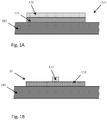
- a method for forming a nanopore in a semiconductor fin will now be described with reference to figures 1a-e , illustrating vertical cross sections taken along the length direction of the fin structure.
- Figure 1a shows a fin structure 100 comprising a bottom layer 110 and a top layer 120 arranged on a substrate 180.
- the bottom layer 110 may for example be formed of Si, such as of a SOI wafer, and the top layer 120 of for example SiO 2 , Si 3 N 4 or other materials which, preferably, provides an etch selectivity relative the material of the bottom layer 110.
- the bottom layer 110 and the top layer 120 may be provided in the form of a stack, which may be patterned into one or several fin structures 100 by means of a fin etch process readily known to a person skilled in the art.
- the top layer 120 may be patterned into a pillar structure 122 as shown in figure 1b .
- This may for example be achieved by means of a line mask (not shown) provided across the fin structure 100 and a following etch process, leaving a pillar or dot shaped mask structure 122 on top of the fin 20 formed by the bottom layer 110.
- the position of the line mask in the length direction of the fin structure 100 determines the alignment of the pillar structure 122 along the fin 20, whereas the pillar structure 122 is self-aligned in the lateral direction (i.e., the width direction) of the fin 20.
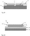
- the pillar 122 has been embedded in a filler layer 130, which for example may be formed of a dielectric filling material such as Si 3 N 4 of SiO 3 .
- the top surface of the structure has been planarized, for example by means of a chemical-mechanical planarization (CMP) process.
- CMP chemical-mechanical planarization
- Figure 1d shows the structure after the pillar 122 has been removed, leaving an aperture 140 that can be used as an etch mask for the resulting nanopore 10.
- the pillar 122 may hence be referred to as a sacrificial pillar 122.
- the material of the pillar 122 may for example be etched in a wet etch process, such as TMAH in case the pillar 122 is formed of for example amorphous Si.
- TMAH etch is used in combination with an etch stop layer separating the pillar 122 and the underlying fin material.
- the pattern defined by the aperture 140 in the filler material layer 130 may then be transferred into the fin 20 to form the nanopore 10.
- An example of the resulting device is illustrated in figure 1e , depicting the semiconductor fin 20 when provided with the nanopore 10 extending in a top-bottom direction of the fin 20.
- the nanopore 10 is self-aligned in the width direction of the fin 20. The self-alignment is achieved due to the use of the sacrificial pillar 122 which is formed of the top layer 120 of the fin structure 100.
- Figure 2a shows a cross sectional side view of a fin structure 200 comprising a bottom layer 210 of for example Si, arranged on a substrate comprising a dielectric layer 284, such as for example SiO 2 , and a Si layer 282.
- the bottom layer 210, the dielectric layer 284 and the Si layer 282 may in some examples be formed of an SOI wafer.
- the fin structure 200 may further comprise a first mask material 224 and a second mask material 226, which together may form the top layer 220 of the fin structure 200.
- the first mask material 224 may be arranged between the bottom layer 210 and the second mask material 226 so as to form an interface between the top layer 220 and the bottom layer 210.
- the top layer 210 may be referred to as a dual mask.
- the first mask material 224 may in some examples be a dielectric such as SiO 2 , Si 3 N 4 , SiOC or SiON.
- the second mask material 226 may be amorphous Si, TiN, Si 3 N 4 , SiO 2 , SiOC or SiON, depending on the type of material used in the first mask 224.
- the first and second mask materials 224, 226 are selected such that the combination allows for an etch selectivity between the materials, which advantageously allows for the first mask material 224 to act as an etch stop layer during the formation of the pillar 222.
- the first mask material is SiO 2 and the second mask material amorphous Si.
- the forming of the pillar 222 requires the top layer, and in this example the second mask material 226, to be patterned into the desired structure.
- the patterning may for example be performed by means of a lithography and etching.
- a hard mask of for example spin-on-carbon (SoC) and spin-on-glass (SoG) may be used (not shown).
- DARC SiOC
- APF carbon film stack.
- Photoresist may be employed to pattern the SoC and SoG layers into a line mask 250 that can be used when cutting the second mask material 226 of the fin structure 200 into a self-aligned pillar or dot structure, using the fist mask material 224 as an etch stop.
- Figure 2b shows a top view of the fin structure 200 of figure 2a , in which the line mask 250 crosses the fin structure 200 in a substantially orthogonal manner.
- FIG. 2c A perspective view of the fin structure 200 is shown in figure 2c .
- the fin structure 200 comprises a fin 20 formed of the bottom layer 210, a pillar 222 arranged on top of the fin 20, and the etch stop layer 224 arranged in between.
- the figure indicates that the etch stop layer 224 has been slightly etched back during the forming of the pillar 222.
- the pillar 222 may as well be formed without the intermediate etch stop layer 224, i.e., formed from a stack comprising only the bottom layer and the top layer. In that case, it might be advantageous to use a slightly thicker bottom layer so as to compensate for possible etch back effects.
- Figure 2d is a cross sectional side view of the fin shown in figure 2c , after the pillar 222 has been embedded in the filler material 230 and replaced by the aperture 240.
- the aperture 240 may be lined with a spacer material 260 provided by for example oxidation or ALD.
- the spacer material 260 may be added so as to reduce the diameter of the aperture 260 and thereby enable a smaller nanopore 10 to be formed in the fin 20.
- the spacer material 260 may be provided on all sidewalls of the aperture 240, which hence may have a width or diameter that is smaller than the width of the fin 20.
- the spacer material 260 may for example be a dielectric such as SiO 2 , Si 3 N 4 , SiOC, TiO 2 , ZrO 2 or HfO 2 or a metal such as TiN, TaN or AIN.
- Figure 2e is a cross sectional top view of the fin 20 shown in figure 2d , taken along the line A-A'.
- the nanopore may be centrally located in the width direction of the fin 20, allowing a polymer such as e.g. a DNA or RNA strand to pass through the fin and thereby form a channel between the drain region 22 and the source region 24 of the fin 20.
- the fin 20 may have a width of about 10 nm and a height of about 10 nm to about 20 nm.
- the nanopore 10 may in the present example have a width of about 5 nm.
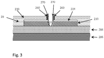
- FIG. 3 illustrates a semiconductor fin 20 according to another example.
- the semiconductor fin 20 may be similarly configured as the previously described embodiments, but differ in that the nanopore 10 is provided with a tapered or funnel shaped profile. As shown in the present figure, the opening 10 may decrease towards the base of the fin 20.
- This tapered profile may for example be achieved by a RIE process, in which etching is cycled with sidewall passivation.
- an anisotropic wet etch such as e.g. orientation dependent KOH etch of Si, may be employed to provide a V-shaped profile of the opening 10.
- the nanopore 10 may be provided with a spacer material 270 lining the sidewalls of the nanopore 10.
- the spacer material 270 may be similar to the one used for the aperture 140, and allows for the diameter of the pore 10 to be even further decreased.
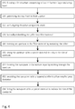
- Figure 4 is a schematic outline of a method according to embodiments described above.
- the method may comprise the steps of providing S10 a fin structure comprising at least a bottom layer and a top layer, patterning S20 the top layer to form a pillar, laterally embedding S30 the pillar in a filler material, forming S40 an aperture in the filler material by removing the pillar, and forming S50 the nanopore in the bottom layer by etching through the aperture.
- the patterning S20 the top layer to form a pillar may include a self-aligning S22 of the pillar using a line mask.
- the aperture may be lied S42 with a spacer material to reduce the size of the aperture and hence the nanopore.
- the nanopore itself, which may be lined S54 with the same or a similar material.
- the nanopore additionally, or alternatively, may be provided with a tapered S52 profile so as to allow for an even smaller pore diameter to be achieved.
Landscapes
- Engineering & Computer Science (AREA)
- Life Sciences & Earth Sciences (AREA)
- Health & Medical Sciences (AREA)
- Chemical & Material Sciences (AREA)
- Physics & Mathematics (AREA)
- Biomedical Technology (AREA)
- Analytical Chemistry (AREA)
- Molecular Biology (AREA)
- General Health & Medical Sciences (AREA)
- Biochemistry (AREA)
- Immunology (AREA)
- Organic Chemistry (AREA)
- Proteomics, Peptides & Aminoacids (AREA)
- Spectroscopy & Molecular Physics (AREA)
- Biophysics (AREA)
- Pathology (AREA)
- General Physics & Mathematics (AREA)
- Manufacturing & Machinery (AREA)
- Microelectronics & Electronic Packaging (AREA)
- Wood Science & Technology (AREA)
- Nanotechnology (AREA)
- Zoology (AREA)
- Hematology (AREA)
- Food Science & Technology (AREA)
- Medicinal Chemistry (AREA)
- Urology & Nephrology (AREA)
- Chemical Kinetics & Catalysis (AREA)
- Microbiology (AREA)
- Electrochemistry (AREA)
- Bioinformatics & Cheminformatics (AREA)
- General Engineering & Computer Science (AREA)
- Genetics & Genomics (AREA)
- Biotechnology (AREA)
- Thin Film Transistor (AREA)
- General Chemical & Material Sciences (AREA)
- Crystallography & Structural Chemistry (AREA)
- Insulated Gate Type Field-Effect Transistor (AREA)
Priority Applications (2)
| Application Number | Priority Date | Filing Date | Title |
|---|---|---|---|
| EP18159987.9A EP3536660A1 (de) | 2018-03-05 | 2018-03-05 | Selbstausgerichtete nanopore auf rippe |
| US16/292,139 US20190271660A1 (en) | 2018-03-05 | 2019-03-04 | Nanopore formed through fin by self-alignment |
Applications Claiming Priority (1)
| Application Number | Priority Date | Filing Date | Title |
|---|---|---|---|
| EP18159987.9A EP3536660A1 (de) | 2018-03-05 | 2018-03-05 | Selbstausgerichtete nanopore auf rippe |
Publications (1)
| Publication Number | Publication Date |
|---|---|
| EP3536660A1 true EP3536660A1 (de) | 2019-09-11 |
Family
ID=61569102
Family Applications (1)
| Application Number | Title | Priority Date | Filing Date |
|---|---|---|---|
| EP18159987.9A Withdrawn EP3536660A1 (de) | 2018-03-05 | 2018-03-05 | Selbstausgerichtete nanopore auf rippe |
Country Status (2)
| Country | Link |
|---|---|
| US (1) | US20190271660A1 (de) |
| EP (1) | EP3536660A1 (de) |
Cited By (1)
| Publication number | Priority date | Publication date | Assignee | Title |
|---|---|---|---|---|
| EP4075131A1 (de) * | 2021-04-16 | 2022-10-19 | Imec VZW | Nanoporentransistor für biosensorik |
Families Citing this family (1)
| Publication number | Priority date | Publication date | Assignee | Title |
|---|---|---|---|---|
| US11674947B2 (en) | 2020-06-13 | 2023-06-13 | International Business Machines Corporation | Nanopore structures |
Citations (2)
| Publication number | Priority date | Publication date | Assignee | Title |
|---|---|---|---|---|
| WO2012044857A2 (en) * | 2010-09-30 | 2012-04-05 | California Institute Of Technology | Devices and methods for sequencing nucleic acids |
| US20130299448A1 (en) * | 2012-05-11 | 2013-11-14 | International Business Machines Corporation | Fabricate self-formed nanometer pore array at wafer scale for dna sequencing |
Family Cites Families (1)
| Publication number | Priority date | Publication date | Assignee | Title |
|---|---|---|---|---|
| US9034637B2 (en) * | 2007-04-25 | 2015-05-19 | Nxp, B.V. | Apparatus and method for molecule detection using nanopores |
-
2018
- 2018-03-05 EP EP18159987.9A patent/EP3536660A1/de not_active Withdrawn
-
2019
- 2019-03-04 US US16/292,139 patent/US20190271660A1/en not_active Abandoned
Patent Citations (2)
| Publication number | Priority date | Publication date | Assignee | Title |
|---|---|---|---|---|
| WO2012044857A2 (en) * | 2010-09-30 | 2012-04-05 | California Institute Of Technology | Devices and methods for sequencing nucleic acids |
| US20130299448A1 (en) * | 2012-05-11 | 2013-11-14 | International Business Machines Corporation | Fabricate self-formed nanometer pore array at wafer scale for dna sequencing |
Non-Patent Citations (1)
| Title |
|---|
| RETO SCHOCH ET AL: "Transport phenomena in nanofluidics", REVIEWS OF MODERN PHYSICS, vol. 80, no. 3, 1 July 2008 (2008-07-01), pages 839 - 883, XP055014035, ISSN: 0034-6861, DOI: 10.1103/RevModPhys.80.839 * |
Cited By (2)
| Publication number | Priority date | Publication date | Assignee | Title |
|---|---|---|---|---|
| EP4075131A1 (de) * | 2021-04-16 | 2022-10-19 | Imec VZW | Nanoporentransistor für biosensorik |
| US12188895B2 (en) | 2021-04-16 | 2025-01-07 | Imec Vzw | Nanopore transistor for biosensing |
Also Published As
| Publication number | Publication date |
|---|---|
| US20190271660A1 (en) | 2019-09-05 |
Similar Documents
| Publication | Publication Date | Title |
|---|---|---|
| US9490129B2 (en) | Integrated circuits having improved gate structures and methods for fabricating same | |
| US9299777B2 (en) | Gate-all-around nanowire MOSFET and method of formation | |
| US10090157B2 (en) | Semiconductor device and manufacturing method thereof | |
| KR102130420B1 (ko) | P형 핀펫 및 n형 핀펫에 대한 향상된 성능을 위한 하이브리드 기법 | |
| US10294101B2 (en) | Semiconductor arrangement with one or more semiconductor columns | |
| US9165770B2 (en) | Methods for fabricating integrated circuits using improved masks | |
| US8404592B2 (en) | Methods for fabricating FinFET semiconductor devices using L-shaped spacers | |
| US10177037B2 (en) | Methods of forming a CT pillar between gate structures in a semiconductor | |
| US9209038B2 (en) | Methods for fabricating integrated circuits using self-aligned quadruple patterning | |
| US9947743B2 (en) | Structures and methods for long-channel devices in nanosheet technology | |
| EP2887399B1 (de) | Verfahren zur Herstellung einer Transistorvorrichtung und zugehörige Vorrichtung | |
| US9941118B2 (en) | Dense vertical nanosheet | |
| US10192956B2 (en) | Method for producing fin structures of a semiconductor device in a substrate | |
| US20160071930A1 (en) | Multiple directed self-assembly material mask patterning for forming vertical nanowires | |
| US12237397B2 (en) | Partial directional etch method and resulting structures | |
| US9209086B2 (en) | Low temperature salicide for replacement gate nanowires | |
| US20190271660A1 (en) | Nanopore formed through fin by self-alignment | |
| US20240339455A1 (en) | Semiconductor device structure and methods of forming the same | |
| US10685847B2 (en) | Vertical nanowires formed on upper fin surface | |
| US12490483B2 (en) | Semiconductor devices and methods of manufacturing thereof | |
| US20180082852A1 (en) | Fin patterning for a fin-type field-effect transistor | |
| US9865682B2 (en) | Directed self-assembly material etch mask for forming vertical nanowires | |
| US9891189B2 (en) | Techniques for fabricating horizontally aligned nanochannels for microfluidics and biosensors | |
| US12188895B2 (en) | Nanopore transistor for biosensing | |
| US20250372393A1 (en) | Semiconductor devices and methods of making semiconductor devices |
Legal Events
| Date | Code | Title | Description |
|---|---|---|---|
| PUAI | Public reference made under article 153(3) epc to a published international application that has entered the european phase |
Free format text: ORIGINAL CODE: 0009012 |
|
| STAA | Information on the status of an ep patent application or granted ep patent |
Free format text: STATUS: THE APPLICATION HAS BEEN PUBLISHED |
|
| AK | Designated contracting states |
Kind code of ref document: A1 Designated state(s): AL AT BE BG CH CY CZ DE DK EE ES FI FR GB GR HR HU IE IS IT LI LT LU LV MC MK MT NL NO PL PT RO RS SE SI SK SM TR |
|
| AX | Request for extension of the european patent |
Extension state: BA ME |
|
| STAA | Information on the status of an ep patent application or granted ep patent |
Free format text: STATUS: REQUEST FOR EXAMINATION WAS MADE |
|
| 17P | Request for examination filed |
Effective date: 20200309 |
|
| RBV | Designated contracting states (corrected) |
Designated state(s): AL AT BE BG CH CY CZ DE DK EE ES FI FR GB GR HR HU IE IS IT LI LT LU LV MC MK MT NL NO PL PT RO RS SE SI SK SM TR |
|
| STAA | Information on the status of an ep patent application or granted ep patent |
Free format text: STATUS: EXAMINATION IS IN PROGRESS |
|
| 17Q | First examination report despatched |
Effective date: 20201112 |
|
| STAA | Information on the status of an ep patent application or granted ep patent |
Free format text: STATUS: THE APPLICATION IS DEEMED TO BE WITHDRAWN |
|
| 18D | Application deemed to be withdrawn |
Effective date: 20210323 |