EP3534553A1 - Amplified multistage demultiplexer - Google Patents
Amplified multistage demultiplexer Download PDFInfo
- Publication number
- EP3534553A1 EP3534553A1 EP18215219.9A EP18215219A EP3534553A1 EP 3534553 A1 EP3534553 A1 EP 3534553A1 EP 18215219 A EP18215219 A EP 18215219A EP 3534553 A1 EP3534553 A1 EP 3534553A1
- Authority
- EP
- European Patent Office
- Prior art keywords
- optical
- signal
- signals
- stage
- filters
- Prior art date
- Legal status (The legal status is an assumption and is not a legal conclusion. Google has not performed a legal analysis and makes no representation as to the accuracy of the status listed.)
- Granted
Links
Images





Classifications
-
- G—PHYSICS
- G02—OPTICS
- G02B—OPTICAL ELEMENTS, SYSTEMS OR APPARATUS
- G02B6/00—Light guides; Structural details of arrangements comprising light guides and other optical elements, e.g. couplings
- G02B6/24—Coupling light guides
- G02B6/26—Optical coupling means
- G02B6/28—Optical coupling means having data bus means, i.e. plural waveguides interconnected and providing an inherently bidirectional system by mixing and splitting signals
- G02B6/293—Optical coupling means having data bus means, i.e. plural waveguides interconnected and providing an inherently bidirectional system by mixing and splitting signals with wavelength selective means
- G02B6/29379—Optical coupling means having data bus means, i.e. plural waveguides interconnected and providing an inherently bidirectional system by mixing and splitting signals with wavelength selective means characterised by the function or use of the complete device
- G02B6/2938—Optical coupling means having data bus means, i.e. plural waveguides interconnected and providing an inherently bidirectional system by mixing and splitting signals with wavelength selective means characterised by the function or use of the complete device for multiplexing or demultiplexing, i.e. combining or separating wavelengths, e.g. 1xN, NxM
-
- H—ELECTRICITY
- H04—ELECTRIC COMMUNICATION TECHNIQUE
- H04B—TRANSMISSION
- H04B10/00—Transmission systems employing electromagnetic waves other than radio-waves, e.g. infrared, visible or ultraviolet light, or employing corpuscular radiation, e.g. quantum communication
- H04B10/60—Receivers
-
- H—ELECTRICITY
- H04—ELECTRIC COMMUNICATION TECHNIQUE
- H04J—MULTIPLEX COMMUNICATION
- H04J14/00—Optical multiplex systems
- H04J14/02—Wavelength-division multiplex systems
- H04J14/0201—Add-and-drop multiplexing
- H04J14/0202—Arrangements therefor
-
- H—ELECTRICITY
- H04—ELECTRIC COMMUNICATION TECHNIQUE
- H04J—MULTIPLEX COMMUNICATION
- H04J14/00—Optical multiplex systems
- H04J14/02—Wavelength-division multiplex systems
- H04J14/0201—Add-and-drop multiplexing
- H04J14/0202—Arrangements therefor
- H04J14/0209—Multi-stage arrangements, e.g. by cascading multiplexers or demultiplexers
-
- H—ELECTRICITY
- H04—ELECTRIC COMMUNICATION TECHNIQUE
- H04J—MULTIPLEX COMMUNICATION
- H04J14/00—Optical multiplex systems
- H04J14/02—Wavelength-division multiplex systems
- H04J14/03—WDM arrangements
- H04J14/0307—Multiplexers; Demultiplexers
Definitions
- the present disclosure generally relates to demultiplexers, and more particularly to signal quality and demultiplexers.
- Multiplexing involves combining multiple signals into a single signal for distribution over a shared medium. For example, multiple optical signals having different wavelengths can be combined into a single combined optical signal, which is transmittable over a single fiber optic channel. When a combined signal is received, the individual signals are separated from each other in a process called demultiplexing. These signals can undergo loss caused by the components used to process and route the signals.
- the signal-to-noise ratio (SNR) can further be degraded by noise added by the components or from external interference sources.
- SNR signal-to-noise ratio
- To address signal degradation more sensitive signal detectors can be implemented. However, the sensitive signal detectors' voltage requirements introduce noise and further degrade SNR.
- a receiver can include a multistage demultiplexer that has integrated amplifiers and a plurality of filter stages.
- the location of the integrated amplifiers within the demultiplexer can vary according to design considerations. If the amplifiers are placed after an initial stage that initially processes the multiplexed signal, the amplifiers can benefit from stronger signal strength, as the amplifiers are higher up the loss chain. However, the multiplexed signal may have an optical bandwidth that exceeds available amplifier optical bandwidths.
- the amplifiers are integrated in the demultiplexer nearer to the last stage so the amplifiers can improve gain of narrower optical bandwidth signals (e.g., each amplifier may amplify an individual signal).
- the demultiplexer can be configured for different numbers of channels, such as two, four, or eight channels. Further, the demultiplexer can have different numbers of stages, with integrated amplifiers being located nearer to the input or output of the demultiplexer based on design considerations (e.g., amplifier optical bandwidth, amplifier saturation power, signal strengths, number of channels, etc.).
- FIG. 1 shows an example wavelength-division multiplexing (WDM) architecture 100 for implementing an amplifying optical demultiplexer, according to some example embodiments.
- the transmitter 105 can receive or otherwise generate a plurality of signals.
- the transmitter 105 can comprise a T1 transmitter 106A that generates an A-signal, a T2 transmitter 106B that generates B-signal, a T3 transmitter 106C that generates C-signal, and a T4 transmitter 106D that generates D-signal.
- the transmitter 105 does not generate the signals but instead receives signals from other sources for routing over a network, as is appreciated by one of ordinary skill in the art.
- the plurality of signals can be combined into a single combined signal 115 using a multiplexer 110 ("MUX").
- the combined signal 115 can be transmitted over a shared medium (e.g., a fiber-optic channel) to a receiver 125 at a remote destination.
- a demultiplexer (“DEMUX") 120 decodes (e.g., splits, separates) the combined signal 115 back into the plurality of individual signals.
- the plurality of individual signals can be detected by receiver detectors, e.g. D1 detector 126A, D2 detector 126B, D3 detector 126C, D4 detector 126D.
- each of the receivers can be a PIN-based photodetector (e.g., photodiode) that can detect an individual optical signal from the demultiplexer 120.
- the receiver 125 may then transmit the received signals to further destinations for routing or processing.
- FIG. 1 shows a WDM architecture 100 in which a transmitter 105 transmits all signals to a receiver 125
- the architecture 100 can be bidirectional over one or more of the channels.
- transmitter 105 can be replaced by a bidirectional collection of transponders that have an ability to send and receive over the channels.
- the receiver 125 can be replaced by an additional bidirectional collection of transponders that also have the ability to send and receive over the channels.
- FIG. 1 illustrates a four-channeled WDM architecture, it is appreciated by one of ordinary skill in the art that other numbers of channels (e.g., 2-channel, 8-channel) can likewise be implemented to achieve similar results.
- Avalanche photodiodes can be implemented as receiver detectors to increase sensitivity; however, APDs have several disadvantages. In particular, APDs tend to be noisier than PIN-photodetectors. Further, APDs tend to have higher voltage requirements to bias the diodes, which can lead to harmful noise and saturation effects. It is also difficult to achieve high electrical bandwidth operation. Providing high bias voltage is not easily achieved with integrated receiver circuit architectures.
- Optical amplifiers can be added to the receiver to increase signal gain.
- adding optical amplifiers to the receiver can introduce further noise (e.g., Amplified Spontaneous Emission (ASE)*Signal (Sig), ASE*ASE, ASE shotnoise) and can also introduce harmful saturation effects.
- ASE Amplified Spontaneous Emission
- Sig Signal-to-Signal
- ASE*ASE ASE*ASE
- ASE shotnoise can also introduce harmful saturation effects.
- an optical amplifier is placed before the demultiplexer (e.g., demultiplexer 120)
- the amplifier must provide gain for the entire optical bandwidth of the incoming WDM signal (e.g., combined signal 115), which can have an optical bandwidth size that exceeds what many amplifiers support.
- providing gain for the entire optical bandwidth of a WDM signal is difficult and/or not practical.
- amplifying a multitude of input signals can saturate the gain material due to the increased power at the amplifier input and cause distortion and cross
- a demultiplexer e.g., demultiplexer 120
- a demultiplexer e.g., demultiplexer 120
- One challenge arises from the fact that some demultiplexers cause signal loss, which directly lowers the SNR. If the degraded SNR is input into an amplifier, the noise is increased along with the signal, which can lead to poor results in the detector (e.g., the photodiode).
- An additional challenge arises from broadband optical noise (e.g., broadband ASE) from the amplifiers themselves. If the amplifiers are placed before the demultiplexer, the components of the demultiplexer, such as filters in the first stage, can filter out the broadband noise. However, if the amplifiers are located after the demultiplexer, the broadband noise (e.g., ASE*ASE optical beat noise, ASE shotnoise) is input into the detector, further degrading SNR.
- broadband noise e.g., ASE*ASE optical beat noise, ASE shotnoise
- the demultiplexer 120 can be configured as an amplifying optical demultiplexer that has a plurality of filter stages, with amplifiers being directly integrated between the stages. Generally, a combined signal can be split into constituent signals, which can in turn be amplified by optical amplifiers.
- the amplifying optical demultiplexer is integrated into a chip-integrated WDM receiver.
- the receiver chip can be formed from a base carrier wafer material comprising silicon, silica, and/or InP or other semiconductor materials.
- the amplifying optical demultiplexer can include passive waveguides as channels that are formed out of the base wafer.
- the amplifiers are semiconductor optical amplifiers (SOAs) that consist of a waveguide of the active semiconductor material.
- the SOAs can be integrated within the base carrier wafer by means of regrowth, heterogeneous, or hybrid integration, according to some example embodiments.
- the optical signal light can be coupled from the passive waveguide in the demultiplexer (e.g., stage 1 filters) to the active semiconductor waveguide of the SOA, and back to the passive waveguides in the demultiplexer (e.g., additional filters in other stages).
- FIG. 2 illustrates an amplifying optical demultiplexer 200, according to some example embodiments.
- the demultiplexer 200 is an example embodiment of demultiplexer 120 in which the demultiplexer 200 is designed to separate four CWDM (course wavelength-division multiplexing) channels spaced 20 nanometers (nm) apart.
- the demultiplexer 200 can receive a combined input signal 201.
- the combined input signal 201 may have a plurality of sub-signals, e.g., signal A, signal B, signal C, and signal D, as discussed above.
- the demultiplexer 200 comprises a plurality of stages, such as a first stage 203, a second stage 207, and a third stage 237.
- Each of the stages 203, 207, 237 can include one or more finite impulse response (FIR) filters (e.g., multistage or higher order FIR filters) and or infinite impulse response (IIR) filters, as discussed in further detail below.
- FIR finite impulse response
- the first stage 203 has a stage 1 filter 205 that separates the combined signal into a first composite signal (e.g., A, C composite signal) on a first waveguide, where the wave guides are denoted by dashed lines.
- the stage 1 filter 205 further separates the combined input signal 201 into a second composite signal (e.g., B, D composite signal) on another wave guide.
- the second stage 207 has a plurality of stage 2 filters including stage 2 filter 210 and stage 2 filter 215.
- the stage 2 filter 210 receives the first composite signal and separates it into two individual signals: signal A and signal C.
- Each of the individual signals generated from the second stage 207 can be amplified by a plurality of integrated SOAs that have been integrated into the demultiplexer 200 as internal components, such as SOAs 220-235. Each of the SOAs 220-235 increases the gain of an individual signal.
- the third stage 237 can be used to further refine or otherwise suppress unwanted noise in the signals (e.g., crosstalk, broad spectrum white noise, noise added by the amplifiers).
- the third stage 237 includes stage 3 filters 240-255, each of which further filters and outputs individual signals 256-262.
- the further filtered individual signals 256-262 from the third stage 237 can then be output to receivers, e.g., photodiodes, for detection and further processing or routing.
- demultiplexer 200 One advantage of demultiplexer 200 is that the optical bandwidth and saturation requirements placed on the SOAs 220-235 are reasonable as each amplifier is managing an individual signal, not the entire four channel WDM signal. Further, the demultiplexer 200 can filter out ⁇ 3dB of the broadband optical ASE spectrum, thereby reducing the ASE*ASE beat noise in the receiver. Furthermore, the optical-SNR of the demultiplexer 200 is improved since the loss of the third filter stage 237 does not contribute to the degradation of the optical-SNR.
- demultiplexer 200 does not include a third stage 237. That is, for example, the demultiplexer 200 only includes the first stage 203, the second stage 207, and the SOAs 220-235, and the additional refining of signals in the third stage 237 is omitted. For instance, after the individual signals are amplified by the SOAs 220-235 the amplified individual signals are output from demultiplexer 200.
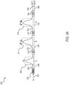
- FIG. 3A shows an example filter 300 that can be implemented in the stage 1 filter 205, according to some example embodiments.
- the filter 300 is a higher-order Mach-Zehnder Interferometer (MZI) filter comprising a 1x2 multimode interferometer (MMI) coupler 305 that receives a single input signal 303 and outputs signals to a first channel 325 and second channel 330.
- MZI Mach-Zehnder Interferometer
- MMI multimode interferometer
- the first channel 325 has three delay stages 306, 311, and 316; with a first delay stage 306 having a length value ⁇ L, and the two following delay stages 311 and 316 being twice as long, 2* ⁇ L.
- the output of directional coupler 320 is two composite signals 335 and 340, as discussed above.
- the length value L is the length of the straight or non-delayed portion of a channel section, where the length ⁇ L is the increased length of a given delay stage.
- the portion of the second channel 330 between the 1x2 MMI coupler 305 and the direct coupler 310 has a length of L, and the length of the first channel between the same couplers has a larger length of ⁇ L.
- FIG. 3B shows an example filter 350 that can be implemented in the stage 1 filter 205 instead of filter 300, according to some example embodiments.
- the filter 350 is a higher-order MZI filter comprising a 1x2 multimode interferometer (MMI) coupler 355 that receives a single input signal 353 and outputs to a first channel 375 and a second channel 377.
- MMI multimode interferometer
- the 1x2 MMI coupler 355 is followed by a sequence of directional couplers 360, 365, and 375, which are connected by the two channels 375 and 377 (e.g., waveguides) having different overall lengths.
- the first channel 375 has a first delay stage 356 of length L
- the second channel 377 includes the second and third delay stages 361 and 366 of filter 350.
- the second delay stage 361 has a length of 2L plus a relative phase shift (e.g., ⁇ ) of light traversing the channel
- the third delay stage 366 has a length of 2L.
- the output of directional coupler 370 is two composite signals 380 and 382 as discussed above. Whether filter 300 of FIG. 3A or filter 350 of FIG. 3B is implemented as a stage 1 filter 205 can depend on different factors, such as the layout or space requirements of other components in demultiplexer 120 or receiver 125.
- FIG. 4A shows an example filter 400 that can be implemented as a stage 2 or stage 3 filter (e.g., stage 2 filter 210, stage 3 filter 240 of FIG. 2 ), according to some example embodiments.
- the filter 400 is a higher-order MZI filter comprising a 1x2 multimode interferometer (MMI) coupler 404 that receives a single input signal 402 and outputs to a first channel 410 and a second channel 412.
- MMI multimode interferometer
- the 1x2 MMI coupler 404 is followed by two directional couplers 406 and 408, which are connected by the two channels 410 and 412 (e.g., waveguides) having different overall lengths.
- MMI multimode interferometer
- the first channel 410 has a first delay stage 414 and a second delay stage 416, with the second delay stage 416 having a length value L, and the first delay stage 414 being half as long, L/2.
- the output of directional coupler 405 can include a first composite signal 420 and a second composite signal 422, as discussed above.
- FIG. 4B shows an example filter 450 that can be implemented as a stage 2 or stage 3 filter (e.g., stage 2 filter 210, stage 3 filter 240) instead of filter 400 of FIG. 4A , according to some example embodiments.
- the filter 460 is a higher-order MZI filter comprising a 1x2 multimode interferometer (MMI) coupler 454 that receives a single input signal 452 (e.g., a composite signal A/C) and generates two output signals (e.g., signal A and signal C).
- MMI multimode interferometer
- the 1x2 MMI coupler 454 is followed by two directional couplers 456 and 458, which are connected by a first channel 460 and a second channel 462 (e.g., waveguides) having different overall lengths.
- the first channel 460 has a first delay stage464, and the second channel has a second delay stage 466.
- the second delay stage466 has a length of L plus half a wavelength (e.g., ⁇ ), and the first delay stage has a length of L/2.
- the output of directional coupler 458 can include a first composite signal 468 and a second composite signal 470.
- FIG. 5 shows an example filter 500 architecture that can be implemented as a stage 2 or stage 3 filter, according to some example embodiments.
- filter 500 is a single stage MZI filter having a first 1x2 MMI 504 which receives an input signal 502 and outputs to a first channel 508 and a second channel 510.
- the first channel 508 includes a delay stage512, which has a length of L/2.
- the third stage filters can be designed as a narrow band FIR or Infinite Impulse Response (IIR) filter designed to reject a greater portion of the broadband ASE, thereby further reducing the ASE*ASE beat noise contribution in a photodetector.
- IIR Infinite Impulse Response
- An example third-stage optical IIR filter is a ring-filter in drop configuration.
- the narrow band FIR/IIR filters have active control to keep the narrow band filter aligned with the incoming signal wavelength.
- active control is accomplished by monitoring the photodetector current and then aligning accordingly.
- FIG. 6 illustrates an amplifying optical demultiplexer 600, according to some example embodiments.
- the demultiplexer 600 is designed to split four CWDM signals on channels spaced 20 nm apart, with SOAs placed between the first and second stages.
- the demultiplexer 600 comprises a plurality of stages, such as a first stage 603, a second stage 617, and a third stage 627, according to some example embodiments.
- the first stage 603 has a stage 1 filter 605 that separates a combined input signal 601 into two composite signals: a first composite signal that includes signal A and signal B, and a second composite signal that includes signal C and signal D.
- the stage 1 filter 605 is a high/low bandpass filter that separates high signals (e.g., A and B) and low signals (e.g., C and D).
- Each of the composite signals generated from the first stage 603 can be amplified by integrated SOAs that are integrated into the demultiplexer 600 as internal components, such as SOA 610 and 615. That is, for example, SOA 610 amplifies the first composite signal (e.g., signal A/B) and the SOA 615 amplifies the second composite signal (e.g., signal C/D).
- SOA 610 amplifies the first composite signal (e.g., signal A/B)
- the SOA 615 amplifies the second composite signal (e.g., signal C/D).
- the second stage 617 has a plurality of stage 2 filters, including stage 2 filter 620 and stage 2 filter 625.
- stage 2 filter 620 receives the first amplified composite signal and separates the composite signal into two individual signals: signal A and signal B.
- stage 2 filter 625 receives the second composite signal and separates the composite signal into two individual signals: signal C and signal D.
- the third stage 627 can be used to further refine or otherwise suppress unwanted noise in the signals (e.g., crosstalk, broad spectrum white noise, noise added by the amplifiers).
- the third stage 627 includes stage 3 filters 630-645, each of which further filters and outputs individual signals 646-652, as illustrated.
- the further filtered individual signals 646-652 from the third stage 627 can then be output to receivers, e.g., photodiodes, for detection and further processing or routing.
- demultiplexer 600 includes fewer SOAs, which means lower power consumption for the demultiplexer 600 and the receiver generally.
- the trade-off is that the amplifiers must be designed to have enough optical gain bandwidth and saturation power to support two neighboring channels (e.g., composite signal A/B, which are 20 nm apart).
- the SOAs between stage 1 and stage 2 handle non-neighboring signals. That is, for example, stage 1 filter 605 can generate a first composite signal A/C and a second composite signal B/D, which are each input into separate SOAs to increase gain. In those embodiments, even though the SOAs must handle increased optical bandwidth due to the signals no longer being neighbors, the optical bandwidth and saturation requirements are still practical.
- a further advantage of demultiplexer 600 is that the composite signal input into the SOAs has had some of the noise (e.g., ASE-ASE beat noise) filtered out by the filters in the first stage.
- demultiplexer 600 does not include a third stage 627. That is, for example, the demultiplexer 600 only includes the first stage 603, the SOAs 610 and 615, and the second stage 617, and the additional refining of signals in the third stage 627 is omitted. For instance, after second stage 617 separates the amplified composite signals into a plurality of individual signals, the individual signals are output from demultiplexer 600.
- FIG. 7 shows an example flow diagram of a method 700 for generating several signals from a combined signal using an amplifying optical demultiplexer, according to some example embodiments.
- the demultiplexer receives multiple optical signals.
- the multiple optical signals may be combined as a single input signal that can be transmitted over a shared medium, such as a fiber-optic cable.
- an optical filter separates the multiple optical signals.
- the optical filter separates the received multiple optical signals into a first composite signal and a second composite signal, where each of the composite signals further comprise two sub-signals.
- the optical filter can separate the received multiple signals into a plurality of individual signals.
- a plurality of optical amplifiers amplify the separated signals.
- a plurality of additional optical amplifiers further filter the optical signals.
- the plurality of additional optical filters may further filter the optical signals by further separating the signals into individual signals.
- the plurality of additional optical filters may further filter the optical signals by removing or otherwise suppressing unwanted noise in the signals.
- the demultiplexer 120 outputs the individual signals to a plurality detectors (e.g., photodiodes) for further processing and/or routing.
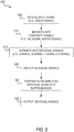
- FIG. 8 shows a flow diagram of a method 800 for generating several signals from a combined signal using an amplifying optical demultiplexer 200 of FIG. 2 , according to some example embodiments.
- the demultiplexer 200 receives an input signal.
- the demultiplexer 200 may receive a composite input signal having four sub-signals: sub-signal A, sub-signal B, sub-signal C, and sub-signal D, each of which may have different wavelengths, spaced by the same amount. That is, for example, sub-signal B can have a wavelength that is 20 nm larger than the wavelength of sub-signal A. Likewise, sub-signal C can have a wavelength it is 20 nm larger than the wavelength of sub-signal B, and so on.
- optical filters in the first stage 203 separate the input signal into composite signals.
- the stage 1 filter 205 separates the input signal A/B/C/D into an A/C signal and a B/D signal.
- optical filters in the second stage 207 further separate the composite signals received from the first stage 203.
- the stage 2 filter 210 can separate the A/C signal into an A-signal and a C-signal.
- the stage 2 filter 215 can separate the B/D signal into a B-signal and a D-signal.
- the individual signals are amplified.
- the amplifier 220 amplifies individual A-signal
- the amplifier 225 amplifies the C-signal
- the amplifier 230 amplifies the B-signal
- the amplifier 235 amplifies D-signal.
- optical filters in a third stage 237 further filter the individual signals to suppress noise such as cross talk from other signals, broad spectrum white noise, or noise added by other components in the demultiplexer 200 (e.g., the SOAs 220-235).
- the demultiplexer 200 outputs the amplified and separated signals.
- the demultiplexer 200 does not include a third stage, as discussed above. In those example embodiments, after the individual signals are amplified at operation 820 the method 800 skips operation 825 (which are third stage filter processes) and goes to operation 830, where the amplified individual signals are output from the demultiplexer.
- FIG. 9 shows a flow diagram of a method 900 for separating several signals from a combined signal using an amplifying optical demultiplexer 600 of FIG. 6 , according to some example embodiments.
- the demultiplexer 600 receives an input signal.
- the demultiplexer 600 may receive a composite input signal having four sub-signals: sub-signal A, sub-signal B, sub-signal C, and sub-signal D.
- Each of the four sub-signals may have different wavelengths that are spaced by the same amount. That is, for example, sub-signal B can have a wavelength that is 20 nm larger than the wavelength of sub-signal A. Likewise, sub-signal C can have a wavelength it is 20 nm larger than the wavelength of sub-signal B, and so on.
- optical filters in the first stage 603 separate the input signal into composite signals.
- the stage 1 filter 605 separates the input signal into an A/B signal and a C/D signal.
- the composite signals are amplified.
- the amplifier 610 amplifies individual A/B signal
- the amplifier 615 amplifies the C/D-signal.
- optical amplifiers in the second stage 617 separate the amplified composite signals into amplified individual signals.
- the stage 2 filter 620 receives the A/B signal and separates the A/B signal into an A-signal and a B-signal.
- the stage 2 filter 625 separates the C/D signal into a C-signal and a D-signal.
- optical filters in the third stage 627 further filter the individual signals to suppress noise, such as crosstalk from other signals, broad spectrum noise, or noise added by other components in the demultiplexer 600(e.g., SOA 610, SOA 615).
- the demultiplexer 600 outputs the individual signals.
- Various embodiments can receive an input signal comprising multiple sub-signals, and separate and amplify the signals within the demultiplexer.
- Some embodiments include a multistage demultiplexer with amplifiers located between a first and second stage.
- Some embodiments include a multistage demultiplexer with amplifiers located between a second and third stage.
- a reference to "A and/or B", when used in conjunction with open-ended language such as “comprising” can refer, in one embodiment, to A only (optionally including elements other than B); in another embodiment, to B only (optionally including elements other than A); in yet another embodiment, to both A and B (optionally including other elements); etc.
- the phrase "at least one,” in reference to a list of one or more elements, should be understood to mean at least one element selected from any one or more of the elements in the list of elements, but not necessarily including at least one of each and every element specifically listed within the list of elements and not excluding any combinations of elements in the list of elements.
- This definition also allows that elements may optionally be present other than the elements specifically identified within the list of elements to which the phrase "at least one" refers, whether related or unrelated to those elements specifically identified.
- At least one of A and B can refer, in one embodiment, to at least one, optionally including more than one, A, with no B present (and optionally including elements other than B); in another embodiment, to at least one, optionally including more than one, B, with no A present (and optionally including elements other than A); in yet another embodiment, to at least one, optionally including more than one, A, and at least one, optionally including more than one, B (and optionally including other elements); etc.
Landscapes
- Engineering & Computer Science (AREA)
- Computer Networks & Wireless Communication (AREA)
- Signal Processing (AREA)
- Physics & Mathematics (AREA)
- Electromagnetism (AREA)
- General Physics & Mathematics (AREA)
- Optics & Photonics (AREA)
- Optical Communication System (AREA)
- Optical Integrated Circuits (AREA)
Abstract
Description
- The present disclosure generally relates to demultiplexers, and more particularly to signal quality and demultiplexers.
- Multiplexing involves combining multiple signals into a single signal for distribution over a shared medium. For example, multiple optical signals having different wavelengths can be combined into a single combined optical signal, which is transmittable over a single fiber optic channel. When a combined signal is received, the individual signals are separated from each other in a process called demultiplexing. These signals can undergo loss caused by the components used to process and route the signals. The signal-to-noise ratio (SNR) can further be degraded by noise added by the components or from external interference sources. To address signal degradation, more sensitive signal detectors can be implemented. However, the sensitive signal detectors' voltage requirements introduce noise and further degrade SNR.
- Particular aspects are set out in the independent claims. Various optional embodiments are set out in the dependent claims.
- To easily identify the discussion of any particular element or act, the most significant digit or digits in a reference number refer to the figure ("FIG.") number in which that element or act is first introduced.
-
FIG. 1 shows an example architecture for implementing an amplifying optical demultiplexer, according to some example embodiments. -
FIG. 2 illustrates an amplifying optical demultiplexer, according to some example embodiments. -
FIG. 3A shows an example filter that can be implemented in thestage 1 filter, according to some example embodiments. -
FIG. 3B shows an example filter that can be implemented in thestage 1 filter, according to some example embodiments. -
FIG. 4A shows an example filter that can be implemented as astage 2 filter, according to some example embodiments. -
FIG. 4B shows an example filter that can be implemented as astage 2 filter, according to some example embodiments. -
FIG. 5 shows an example filter architecture that can be implemented in astage 3 filter, according to some example embodiments. -
FIG. 6 illustrates an amplifying optical demultiplexer, according to some example embodiments. -
FIG. 7 shows an example flow diagram of a method for implementing an amplifying optical demultiplexer, according to some example embodiments. -
FIG. 8 shows a flow diagram of a method for implementing an amplifying optical demultiplexer, according to some example embodiments. -
FIG. 9 shows a flow diagram of a method for implementing an amplifying optical demultiplexer, according to some example embodiments. - The description that follows includes systems, methods, techniques, and instruction sequences that embody illustrative embodiments of the disclosure. In the following description, for the purposes of explanation, numerous specific details are set forth in order to provide an understanding of various embodiments of the inventive subject matter. It will be evident, however, to those skilled in the art, that embodiments of the inventive subject matter may be practiced without these specific details. In general, well-known instruction instances, protocols, structures, and techniques are not necessarily shown in detail.
- As mentioned above, multiplexed signals can undergo loss, and detectors have difficulty finding a signal buried in noise. Detector sensitivity can be increased, but sensitive detectors have higher power requirements, which can lead to additional noise. To this end, in example embodiments a receiver can include a multistage demultiplexer that has integrated amplifiers and a plurality of filter stages. The location of the integrated amplifiers within the demultiplexer can vary according to design considerations. If the amplifiers are placed after an initial stage that initially processes the multiplexed signal, the amplifiers can benefit from stronger signal strength, as the amplifiers are higher up the loss chain. However, the multiplexed signal may have an optical bandwidth that exceeds available amplifier optical bandwidths. In some embodiments, the amplifiers are integrated in the demultiplexer nearer to the last stage so the amplifiers can improve gain of narrower optical bandwidth signals (e.g., each amplifier may amplify an individual signal). The demultiplexer can be configured for different numbers of channels, such as two, four, or eight channels. Further, the demultiplexer can have different numbers of stages, with integrated amplifiers being located nearer to the input or output of the demultiplexer based on design considerations (e.g., amplifier optical bandwidth, amplifier saturation power, signal strengths, number of channels, etc.).
-
FIG. 1 shows an example wavelength-division multiplexing (WDM)architecture 100 for implementing an amplifying optical demultiplexer, according to some example embodiments. As illustrated, thetransmitter 105 can receive or otherwise generate a plurality of signals. For example, thetransmitter 105 can comprise aT1 transmitter 106A that generates an A-signal, aT2 transmitter 106B that generates B-signal, aT3 transmitter 106C that generates C-signal, and aT4 transmitter 106D that generates D-signal. In some example embodiments, thetransmitter 105 does not generate the signals but instead receives signals from other sources for routing over a network, as is appreciated by one of ordinary skill in the art. - The plurality of signals can be combined into a single combined
signal 115 using a multiplexer 110 ("MUX"). The combinedsignal 115 can be transmitted over a shared medium (e.g., a fiber-optic channel) to areceiver 125 at a remote destination. In thereceiver 125, a demultiplexer ("DEMUX") 120 decodes (e.g., splits, separates) the combinedsignal 115 back into the plurality of individual signals. The plurality of individual signals can be detected by receiver detectors,e.g. D1 detector 126A,D2 detector 126B,D3 detector 126C,D4 detector 126D. For example, each of the receivers can be a PIN-based photodetector (e.g., photodiode) that can detect an individual optical signal from thedemultiplexer 120. Thereceiver 125 may then transmit the received signals to further destinations for routing or processing. - Although
FIG. 1 shows aWDM architecture 100 in which atransmitter 105 transmits all signals to areceiver 125, it is appreciated by one of ordinary skill in the art that thearchitecture 100 can be bidirectional over one or more of the channels. For example,transmitter 105 can be replaced by a bidirectional collection of transponders that have an ability to send and receive over the channels. Likewise, thereceiver 125 can be replaced by an additional bidirectional collection of transponders that also have the ability to send and receive over the channels. Further, the example inFIG. 1 illustrates a four-channeled WDM architecture, it is appreciated by one of ordinary skill in the art that other numbers of channels (e.g., 2-channel, 8-channel) can likewise be implemented to achieve similar results. - One challenge in demultiplexing architectures is to achieve low enough losses to meet the sensitivity requirements of the receiver detectors, such as photodiodes. Avalanche photodiodes (APDs) can be implemented as receiver detectors to increase sensitivity; however, APDs have several disadvantages. In particular, APDs tend to be noisier than PIN-photodetectors. Further, APDs tend to have higher voltage requirements to bias the diodes, which can lead to harmful noise and saturation effects. It is also difficult to achieve high electrical bandwidth operation. Providing high bias voltage is not easily achieved with integrated receiver circuit architectures.
- Optical amplifiers can be added to the receiver to increase signal gain. However, adding optical amplifiers to the receiver can introduce further noise (e.g., Amplified Spontaneous Emission (ASE)*Signal (Sig), ASE*ASE, ASE shotnoise) and can also introduce harmful saturation effects. For example, if an optical amplifier is placed before the demultiplexer (e.g., demultiplexer 120), the amplifier must provide gain for the entire optical bandwidth of the incoming WDM signal (e.g., combined signal 115), which can have an optical bandwidth size that exceeds what many amplifiers support. As such, providing gain for the entire optical bandwidth of a WDM signal is difficult and/or not practical. Furthermore, amplifying a multitude of input signals can saturate the gain material due to the increased power at the amplifier input and cause distortion and crosstalk between signals at the output.
- Placing amplifiers after a demultiplexer (e.g., demultiplexer 120) creates a different set of challenges. One challenge arises from the fact that some demultiplexers cause signal loss, which directly lowers the SNR. If the degraded SNR is input into an amplifier, the noise is increased along with the signal, which can lead to poor results in the detector (e.g., the photodiode). An additional challenge arises from broadband optical noise (e.g., broadband ASE) from the amplifiers themselves. If the amplifiers are placed before the demultiplexer, the components of the demultiplexer, such as filters in the first stage, can filter out the broadband noise. However, if the amplifiers are located after the demultiplexer, the broadband noise (e.g., ASE*ASE optical beat noise, ASE shotnoise) is input into the detector, further degrading SNR.
- To this end, the
demultiplexer 120 can be configured as an amplifying optical demultiplexer that has a plurality of filter stages, with amplifiers being directly integrated between the stages. Generally, a combined signal can be split into constituent signals, which can in turn be amplified by optical amplifiers. In some example embodiments, the amplifying optical demultiplexer is integrated into a chip-integrated WDM receiver. The receiver chip can be formed from a base carrier wafer material comprising silicon, silica, and/or InP or other semiconductor materials. On the chip, the amplifying optical demultiplexer can include passive waveguides as channels that are formed out of the base wafer. In some embodiments, the amplifiers are semiconductor optical amplifiers (SOAs) that consist of a waveguide of the active semiconductor material. The SOAs can be integrated within the base carrier wafer by means of regrowth, heterogeneous, or hybrid integration, according to some example embodiments. The optical signal light can be coupled from the passive waveguide in the demultiplexer (e.g.,stage 1 filters) to the active semiconductor waveguide of the SOA, and back to the passive waveguides in the demultiplexer (e.g., additional filters in other stages). -
FIG. 2 illustrates an amplifyingoptical demultiplexer 200, according to some example embodiments. Thedemultiplexer 200 is an example embodiment ofdemultiplexer 120 in which thedemultiplexer 200 is designed to separate four CWDM (course wavelength-division multiplexing) channels spaced 20 nanometers (nm) apart. As illustrated, thedemultiplexer 200 can receive a combinedinput signal 201. The combinedinput signal 201 may have a plurality of sub-signals, e.g., signal A, signal B, signal C, and signal D, as discussed above. Thedemultiplexer 200 comprises a plurality of stages, such as afirst stage 203, asecond stage 207, and athird stage 237. Each of thestages - As illustrated, the
first stage 203 has astage 1filter 205 that separates the combined signal into a first composite signal (e.g., A, C composite signal) on a first waveguide, where the wave guides are denoted by dashed lines. Thestage 1filter 205 further separates the combinedinput signal 201 into a second composite signal (e.g., B, D composite signal) on another wave guide. Thesecond stage 207 has a plurality ofstage 2filters including stage 2filter 210 andstage 2filter 215. Thestage 2filter 210 receives the first composite signal and separates it into two individual signals: signal A and signal C. Each of the individual signals generated from thesecond stage 207 can be amplified by a plurality of integrated SOAs that have been integrated into thedemultiplexer 200 as internal components, such as SOAs 220-235. Each of the SOAs 220-235 increases the gain of an individual signal. - The
third stage 237 can be used to further refine or otherwise suppress unwanted noise in the signals (e.g., crosstalk, broad spectrum white noise, noise added by the amplifiers). As illustrated, thethird stage 237 includesstage 3 filters 240-255, each of which further filters and outputs individual signals 256-262. The further filtered individual signals 256-262 from thethird stage 237 can then be output to receivers, e.g., photodiodes, for detection and further processing or routing. - One advantage of
demultiplexer 200 is that the optical bandwidth and saturation requirements placed on the SOAs 220-235 are reasonable as each amplifier is managing an individual signal, not the entire four channel WDM signal. Further, thedemultiplexer 200 can filter out ∼3dB of the broadband optical ASE spectrum, thereby reducing the ASE*ASE beat noise in the receiver. Furthermore, the optical-SNR of thedemultiplexer 200 is improved since the loss of thethird filter stage 237 does not contribute to the degradation of the optical-SNR. - In some example embodiments,
demultiplexer 200 does not include athird stage 237. That is, for example, thedemultiplexer 200 only includes thefirst stage 203, thesecond stage 207, and the SOAs 220-235, and the additional refining of signals in thethird stage 237 is omitted. For instance, after the individual signals are amplified by the SOAs 220-235 the amplified individual signals are output fromdemultiplexer 200. -
FIG. 3A shows anexample filter 300 that can be implemented in thestage 1filter 205, according to some example embodiments. As illustrated, thefilter 300 is a higher-order Mach-Zehnder Interferometer (MZI) filter comprising a 1x2 multimode interferometer (MMI)coupler 305 that receives asingle input signal 303 and outputs signals to afirst channel 325 andsecond channel 330. The1x2 MMI coupler 305 is followed by a sequence of directional couplers 310-320, which are connected by the twochannels 325, 330 (e.g., waveguides) having different lengths. In particular, thefirst channel 325 has threedelay stages first delay stage 306 having a length value ΔL, and the two following delay stages 311 and 316 being twice as long, 2*ΔL. In some example embodiments, the output ofdirectional coupler 320 is twocomposite signals second channel 330 between the1x2 MMI coupler 305 and thedirect coupler 310 has a length of L, and the length of the first channel between the same couplers has a larger length of ΔL. -
FIG. 3B shows anexample filter 350 that can be implemented in thestage 1filter 205 instead offilter 300, according to some example embodiments. Thefilter 350 is a higher-order MZI filter comprising a 1x2 multimode interferometer (MMI)coupler 355 that receives asingle input signal 353 and outputs to afirst channel 375 and asecond channel 377. The1x2 MMI coupler 355 is followed by a sequence ofdirectional couplers channels 375 and 377 (e.g., waveguides) having different overall lengths. In particular, thefirst channel 375 has afirst delay stage 356 of length L, and thesecond channel 377 includes the second and third delay stages 361 and 366 offilter 350. Thesecond delay stage 361 has a length of 2L plus a relative phase shift (e.g., π) of light traversing the channel, and thethird delay stage 366 has a length of 2L. In some example embodiments, the output ofdirectional coupler 370 is twocomposite signals filter 300 ofFIG. 3A or filter 350 ofFIG. 3B is implemented as astage 1filter 205 can depend on different factors, such as the layout or space requirements of other components indemultiplexer 120 orreceiver 125. -
FIG. 4A shows anexample filter 400 that can be implemented as astage 2 orstage 3 filter (e.g.,stage 2filter 210,stage 3filter 240 ofFIG. 2 ), according to some example embodiments. As illustrated, thefilter 400 is a higher-order MZI filter comprising a 1x2 multimode interferometer (MMI)coupler 404 that receives asingle input signal 402 and outputs to afirst channel 410 and asecond channel 412. The1x2 MMI coupler 404 is followed by twodirectional couplers channels 410 and 412 (e.g., waveguides) having different overall lengths. In particular, thefirst channel 410 has afirst delay stage 414 and asecond delay stage 416, with thesecond delay stage 416 having a length value L, and thefirst delay stage 414 being half as long, L/2. The output of directional coupler 405 can include a firstcomposite signal 420 and a secondcomposite signal 422, as discussed above. -
FIG. 4B shows anexample filter 450 that can be implemented as astage 2 orstage 3 filter (e.g.,stage 2filter 210,stage 3 filter 240) instead offilter 400 ofFIG. 4A , according to some example embodiments. Thefilter 460 is a higher-order MZI filter comprising a 1x2 multimode interferometer (MMI)coupler 454 that receives a single input signal 452 (e.g., a composite signal A/C) and generates two output signals (e.g., signal A and signal C). The1x2 MMI coupler 454 is followed by twodirectional couplers first channel 460 and a second channel 462 (e.g., waveguides) having different overall lengths. Thefirst channel 460 has a first delay stage464, and the second channel has asecond delay stage 466. The second delay stage466 has a length of L plus half a wavelength (e.g., π), and the first delay stage has a length of L/2. The output ofdirectional coupler 458 can include a firstcomposite signal 468 and a secondcomposite signal 470. -
FIG. 5 shows anexample filter 500 architecture that can be implemented as astage 2 orstage 3 filter, according to some example embodiments. As illustrated,filter 500 is a single stage MZI filter having afirst 1x2 MMI 504 which receives aninput signal 502 and outputs to afirst channel 508 and asecond channel 510. Thefirst channel 508 includes a delay stage512, which has a length of L/2. The channels input into2x2 MMI 506, which generatesoutputs -
FIG. 6 illustrates an amplifyingoptical demultiplexer 600, according to some example embodiments. As illustrated, thedemultiplexer 600 is designed to split four CWDM signals on channels spaced 20 nm apart, with SOAs placed between the first and second stages. Thedemultiplexer 600 comprises a plurality of stages, such as afirst stage 603, asecond stage 617, and athird stage 627, according to some example embodiments. Thefirst stage 603 has astage 1 filter 605 that separates a combinedinput signal 601 into two composite signals: a first composite signal that includes signal A and signal B, and a second composite signal that includes signal C and signal D. In this example embodiment, thestage 1 filter 605 is a high/low bandpass filter that separates high signals (e.g., A and B) and low signals (e.g., C and D). - Each of the composite signals generated from the
first stage 603 can be amplified by integrated SOAs that are integrated into thedemultiplexer 600 as internal components, such asSOA SOA 610 amplifies the first composite signal (e.g., signal A/B) and theSOA 615 amplifies the second composite signal (e.g., signal C/D). - The
second stage 617 has a plurality ofstage 2 filters, includingstage 2filter 620 andstage 2filter 625. Thestage 2filter 620 receives the first amplified composite signal and separates the composite signal into two individual signals: signal A and signal B. Likewise, thestage 2filter 625 receives the second composite signal and separates the composite signal into two individual signals: signal C and signal D. - The
third stage 627 can be used to further refine or otherwise suppress unwanted noise in the signals (e.g., crosstalk, broad spectrum white noise, noise added by the amplifiers). As illustrated, thethird stage 627 includesstage 3 filters 630-645, each of which further filters and outputs individual signals 646-652, as illustrated. The further filtered individual signals 646-652 from thethird stage 627 can then be output to receivers, e.g., photodiodes, for detection and further processing or routing. - One advantage of
demultiplexer 600 is that it includes fewer SOAs, which means lower power consumption for thedemultiplexer 600 and the receiver generally. The trade-off is that the amplifiers must be designed to have enough optical gain bandwidth and saturation power to support two neighboring channels (e.g., composite signal A/B, which are 20 nm apart). In some embodiments, the SOAs betweenstage 1 andstage 2 handle non-neighboring signals. That is, for example,stage 1 filter 605 can generate a first composite signal A/C and a second composite signal B/D, which are each input into separate SOAs to increase gain. In those embodiments, even though the SOAs must handle increased optical bandwidth due to the signals no longer being neighbors, the optical bandwidth and saturation requirements are still practical. A further advantage ofdemultiplexer 600 is that the composite signal input into the SOAs has had some of the noise (e.g., ASE-ASE beat noise) filtered out by the filters in the first stage. - In some example embodiments,
demultiplexer 600 does not include athird stage 627. That is, for example, thedemultiplexer 600 only includes thefirst stage 603, theSOAs second stage 617, and the additional refining of signals in thethird stage 627 is omitted. For instance, aftersecond stage 617 separates the amplified composite signals into a plurality of individual signals, the individual signals are output fromdemultiplexer 600. -
FIG. 7 shows an example flow diagram of amethod 700 for generating several signals from a combined signal using an amplifying optical demultiplexer, according to some example embodiments. - At
operation 705, the demultiplexer (e.g., thedemultiplexer 120 as shown inFIG. 1 ) receives multiple optical signals. The multiple optical signals may be combined as a single input signal that can be transmitted over a shared medium, such as a fiber-optic cable. Atoperation 710, an optical filter separates the multiple optical signals. For example, atoperation 710 the optical filter separates the received multiple optical signals into a first composite signal and a second composite signal, where each of the composite signals further comprise two sub-signals. As a further example, atoperation 710, the optical filter can separate the received multiple signals into a plurality of individual signals. Atoperation 715, a plurality of optical amplifiers amplify the separated signals. Atoperation 720, a plurality of additional optical amplifiers further filter the optical signals. For example, atoperation 720 the plurality of additional optical filters may further filter the optical signals by further separating the signals into individual signals. Further, according to some example embodiments, atoperation 720 the plurality of additional optical filters may further filter the optical signals by removing or otherwise suppressing unwanted noise in the signals. Atoperation 725, thedemultiplexer 120 outputs the individual signals to a plurality detectors (e.g., photodiodes) for further processing and/or routing. -
FIG. 8 shows a flow diagram of amethod 800 for generating several signals from a combined signal using an amplifyingoptical demultiplexer 200 ofFIG. 2 , according to some example embodiments. Atoperation 805, thedemultiplexer 200 receives an input signal. For example, thedemultiplexer 200 may receive a composite input signal having four sub-signals: sub-signal A, sub-signal B, sub-signal C, and sub-signal D, each of which may have different wavelengths, spaced by the same amount. That is, for example, sub-signal B can have a wavelength that is 20 nm larger than the wavelength of sub-signal A. Likewise, sub-signal C can have a wavelength it is 20 nm larger than the wavelength of sub-signal B, and so on. - At
operation 810, optical filters in thefirst stage 203 separate the input signal into composite signals. For example, thestage 1filter 205 separates the input signal A/B/C/D into an A/C signal and a B/D signal. Atoperation 815, optical filters in thesecond stage 207 further separate the composite signals received from thefirst stage 203. For example, thestage 2filter 210 can separate the A/C signal into an A-signal and a C-signal. Likewise, thestage 2filter 215 can separate the B/D signal into a B-signal and a D-signal. - At
operation 820, the individual signals are amplified. For example, theamplifier 220 amplifies individual A-signal, theamplifier 225 amplifies the C-signal, theamplifier 230 amplifies the B-signal, and theamplifier 235 amplifies D-signal. Atoperation 825, optical filters in athird stage 237 further filter the individual signals to suppress noise such as cross talk from other signals, broad spectrum white noise, or noise added by other components in the demultiplexer 200 (e.g., the SOAs 220-235). Atoperation 830, thedemultiplexer 200 outputs the amplified and separated signals. In some example embodiments, thedemultiplexer 200 does not include a third stage, as discussed above. In those example embodiments, after the individual signals are amplified atoperation 820 themethod 800 skips operation 825 (which are third stage filter processes) and goes tooperation 830, where the amplified individual signals are output from the demultiplexer. -
FIG. 9 shows a flow diagram of amethod 900 for separating several signals from a combined signal using an amplifyingoptical demultiplexer 600 ofFIG. 6 , according to some example embodiments. Atoperation 905, thedemultiplexer 600 receives an input signal. For example, thedemultiplexer 600 may receive a composite input signal having four sub-signals: sub-signal A, sub-signal B, sub-signal C, and sub-signal D. Each of the four sub-signals may have different wavelengths that are spaced by the same amount. That is, for example, sub-signal B can have a wavelength that is 20 nm larger than the wavelength of sub-signal A. Likewise, sub-signal C can have a wavelength it is 20 nm larger than the wavelength of sub-signal B, and so on. - At
operation 910, optical filters in thefirst stage 603 separate the input signal into composite signals. For example, thestage 1 filter 605 separates the input signal into an A/B signal and a C/D signal. - At
operation 920, the composite signals are amplified. For example, theamplifier 610 amplifies individual A/B signal, theamplifier 615 amplifies the C/D-signal. Atoperation 915, optical amplifiers in thesecond stage 617 separate the amplified composite signals into amplified individual signals. For example, thestage 2filter 620 receives the A/B signal and separates the A/B signal into an A-signal and a B-signal. Likewise, thestage 2filter 625 separates the C/D signal into a C-signal and a D-signal. Atoperation 925, optical filters in thethird stage 627 further filter the individual signals to suppress noise, such as crosstalk from other signals, broad spectrum noise, or noise added by other components in the demultiplexer 600(e.g.,SOA 610, SOA 615). Atoperation 930, thedemultiplexer 600 outputs the individual signals. - While various embodiments have been described above, it should be understood that they have been presented by way of example only, and not limitation. Where methods described above indicate certain events occurring in certain order, the ordering of certain events may be modified. Additionally, certain of the events may be performed concurrently in a parallel process when possible, as well as performed sequentially as described above. Accordingly, the specification is intended to embrace all such modifications and variations of the disclosed embodiments that fall within the spirit and scope of the appended claims.
- Therefore, from one perspective, there have been described various configurations for an amplifying optical demultiplexer. Various embodiments can receive an input signal comprising multiple sub-signals, and separate and amplify the signals within the demultiplexer. Some embodiments include a multistage demultiplexer with amplifiers located between a first and second stage. Some embodiments include a multistage demultiplexer with amplifiers located between a second and third stage.
- Further examples of the present disclosure are set out in the following numbered clauses:
- Clause 1 A method of processing optical signal, the method comprising:
- receiving, by a multistage demultiplexer, an input signal having multiple optical signals, the multistage demultiplexer comprising an optical filter in an initial stage and additional optical filters in an additional stage;
- separating the multiple optical signals using the optical filter in the initial stage; generating, using multiple optical amplifiers, amplified optical signals by amplifying the multiple optical signals that have been separated by the optical filter in the initial stage, the multiple optical amplifiers being integrated in the multistage demultiplexer between the optical filter in the initial stage and the additional optical filters in the additional stage; and generating filtered optical signals by filtering the amplified optical signals using the additional optical filters in the additional stage.
-
Clause 2 The method ofclause 1, wherein the multistage demultiplexer further comprises intermediate optical filters in an intermediate stage, the intermediate optical filters being located between the optical filter of the initial stage and the multiple optical amplifiers. -
Clause 3 The method ofclause 2, wherein the optical filter in the initial stage separates the multiple optical signals into a plurality of composite signals, each of the composite signals comprising a plurality of individual signals of different wavelengths. - Clause 4 The method of
clause 3, further comprising: generating, using the intermediate optical filters in the intermediate stage, a plurality of individual signals from the plurality of composite signals. - Clause 5 The method of clause 4, wherein each of the multiple optical amplifiers amplify an individual signal from the plurality of individual signals.
- Clause 6 The method of any preceding clause, wherein the multistage demultiplexer further comprises output optical filters in an output stage, the output optical filters being located after the additional optical filters of the additional stage.
- Clause 7 The method of clause 6, wherein the filtered optical signals generated by the additional optical filters are a plurality of individual signals.
- Clause 8 The method of clause 7, further comprising: generating, using the output optical filters in the output stage, output signals by suppressing noise in the plurality of individual signals.
- Clause 9 The method of
clause 3 or any clause dependent thereon, wherein the amplified optical signals are a plurality of amplified composite signals that are generated from the plurality of composite signals using the multiple optical amplifiers. - Clause 10 The method of any preceding clause, wherein the optical filter comprises a first plurality of optical couplers and each of the additional optical filters comprises a second plurality of optical couplers, the first plurality of optical couplers of the optical filter having at least one optical coupler more than the second plurality of optical couplers of the additional optical filters.
- Clause 11 The method of any preceding clause, wherein the input signal comprises a first signal, a second signal, a third signal, and a fourth signal; and wherein the first signal having a smaller wavelength than the second signal, the second signal having a smaller wavelength than the third signal, the third signal having a smaller wavelength than the first signal.
- Clause 12 The method of clause 11, wherein one of the multiple optical amplifiers amplifies a composite signal comprising the first signal and the second signal, and another of the multiple optical amplifiers amplifies another composite signal comprising the third signal and the fourth signal.
- Clause 13 The method of any preceding clause, wherein one or more of the optical filter or the additional optical filters are: Mach-Zehnder Interferometer (MZI) filters or infinite input response (IIR) filters.
- Clause 14 The method of any preceding clause, wherein the multiple optical amplifiers are semiconductor optical amplifiers (SOAs).
- Clause 15 An optical device for processing optical signal, the optical device comprising: a multistage demultiplexer to receive an input signal having multiple optical signals, the multistage demultiplexer comprising: an optical filter in an initial stage to separate the multiple optical signals; multiple optical amplifiers to generate amplified optical signals by amplifying the multiple optical signals that are separated by the optical filter; and additional optical filters in an additional stage to generate filtered optical signals by filtering the amplified optical signals, the multiple optical amplifiers being integrated in the multistage demultiplexer between the optical filter in the initial stage and the additional optical filters in the additional stage.
- Clause 16 The optical device of clause 15, wherein the multistage demultiplexer further comprises intermediate optical filters in an intermediate stage, the intermediate optical filters being located between the optical filter of the initial stage and the multiple optical amplifiers.
- Clause 17 The optical device of clause 16, wherein the optical filter in the initial stage separates the multiple signals into a first composite signal and a second composite signal; and wherein the intermediate optical filters separate the first composite signal and the second composite signal into a plurality of individual signals.
- Clause 18 The optical device of clause 17, wherein each of the additional optical filters in the additional stage filters one of the plurality of individual signals to suppress noise.
- Clause 19 The optical device of any of clauses 15 to 18, wherein the multistage demultiplexer further comprises output optical filters in an output stage, the output optical filters being located after the additional optical filters of the additional stage.
- Clause 20 The optical device of clause 19, wherein the optical filter in the initial stage separates the multiple signals into a plurality of composite signals; wherein the additional optical filters in the additional stage separate the plurality of composite signals into a plurality of individual optical signals; wherein each of the multiple optical amplifiers amplifies one of the plurality of individual optical signals; and wherein the each of the output optical filters in the output stage filters one of the plurality of individual optical signals to suppress noise.
- All definitions, as defined and used herein, should be understood to control over dictionary definitions, definitions in documents incorporated by reference, and/or ordinary meanings of the defined terms.
- The indefinite articles "a" and "an," as used herein in the specification and in the claims, unless clearly indicated to the contrary, should be understood to mean "at least one."
- The phrase "and/or," as used herein in the specification and in the claims, should be understood to mean "either or both" of the elements so conjoined, i.e., elements that are conjunctively present in some cases and disjunctively present in other cases. Multiple elements listed with "and/or" should be construed in the same fashion, i.e., "one or more" of the elements so conjoined. Other elements may optionally be present other than the elements specifically identified by the "and/or" clause, whether related or unrelated to those elements specifically identified. Thus, as a non-limiting example, a reference to "A and/or B", when used in conjunction with open-ended language such as "comprising" can refer, in one embodiment, to A only (optionally including elements other than B); in another embodiment, to B only (optionally including elements other than A); in yet another embodiment, to both A and B (optionally including other elements); etc.
- As used herein in the specification and in the claims, "or" should be understood to have the same meaning as "and/or" as defined above. For example, when separating items in a list, "or" or "and/or" shall be interpreted as being inclusive, i.e., the inclusion of at least one, but also including more than one, of a number or list of elements, and, optionally, additional unlisted items. Only terms clearly indicated to the contrary, such as "only one of' or "exactly one of," or, when used in the claims, "consisting of," will refer to the inclusion of exactly one element of a number or list of elements. In general, the term "or" as used herein shall only be interpreted as indicating exclusive alternatives (i.e. "one or the other but not both") when preceded by terms of exclusivity, such as "either," "one of," "only one of," or "exactly one of." "Consisting essentially of," when used in the claims, shall have its ordinary meaning as used in the field of patent law.
- As used herein in the specification and in the claims, the phrase "at least one," in reference to a list of one or more elements, should be understood to mean at least one element selected from any one or more of the elements in the list of elements, but not necessarily including at least one of each and every element specifically listed within the list of elements and not excluding any combinations of elements in the list of elements. This definition also allows that elements may optionally be present other than the elements specifically identified within the list of elements to which the phrase "at least one" refers, whether related or unrelated to those elements specifically identified. Thus, as a non-limiting example, "at least one of A and B" (or, equivalently, "at least one of A or B," or, equivalently "at least one of A and/or B") can refer, in one embodiment, to at least one, optionally including more than one, A, with no B present (and optionally including elements other than B); in another embodiment, to at least one, optionally including more than one, B, with no A present (and optionally including elements other than A); in yet another embodiment, to at least one, optionally including more than one, A, and at least one, optionally including more than one, B (and optionally including other elements); etc.
- In the claims, as well as in the specification above, all transitional phrases such as "comprising," "including," "carrying," "having," "containing," "involving," "holding," "composed of," and the like are to be understood to be open-ended, i.e., to mean including but not limited to. Only the transitional phrases "consisting of' and "consisting essentially of' shall be closed or semi-closed transitional phrases, respectively, as set forth in the United States Patent Office Manual of Patent Examining Procedures, Section 2111.03.
Claims (15)
- A method of processing optical signal, the method comprising:receiving, by a multistage demultiplexer, an input signal having multiple optical signals, the multistage demultiplexer comprising an optical filter in an initial stage and additional optical filters in an additional stage;separating the multiple optical signals using the optical filter in the initial stage;generating, using multiple optical amplifiers, amplified optical signals by amplifying the multiple optical signals that have been separated by the optical filter in the initial stage, the multiple optical amplifiers being integrated in the multistage demultiplexer between the optical filter in the initial stage and the additional optical filters in the additional stage; andgenerating filtered optical signals by filtering the amplified optical signals using the additional optical filters in the additional stage.
- The method of claim 1, wherein the multistage demultiplexer further comprises intermediate optical filters in an intermediate stage, the intermediate optical filters being located between the optical filter of the initial stage and the multiple optical amplifiers.
- The method of claim 2, wherein the optical filter in the initial stage separates the multiple optical signals into a plurality of composite signals, each of the composite signals comprising a plurality of individual signals of different wavelengths.
- The method of claim 3, further comprising:generating, using the intermediate optical filters in the intermediate stage, a plurality of individual signals from the plurality of composite signals.
- The method of claim 4, wherein each of the multiple optical amplifiers amplify an individual signal from the plurality of individual signals.
- The method of claim 3 or 4, wherein the amplified optical signals are a plurality of amplified composite signals that are generated from the plurality of composite signals using the multiple optical amplifiers.
- The method of any preceding claim, wherein the multistage demultiplexer further comprises output optical filters in an output stage, the output optical filters being located after the additional optical filters of the additional stage.
- The method of claim 7, wherein the filtered optical signals generated by the additional optical filters are a plurality of individual signals.
- The method of claim 8, further comprising:generating, using the output optical filters in the output stage, output signals by suppressing noise in the plurality of individual signals.
- The method of any preceding claim, wherein the optical filter comprises a first plurality of optical couplers and each of the additional optical filters comprises a second plurality of optical couplers, the first plurality of optical couplers of the optical filter having at least one optical coupler more than the second plurality of optical couplers of the additional optical filters.
- The method of any preceding claim, wherein the input signal comprises a first signal, a second signal, a third signal, and a fourth signal; and
wherein the first signal having a smaller wavelength than the second signal, the second signal having a smaller wavelength than the third signal, the third signal having a smaller wavelength than the first signal. - The method of claim 11, wherein one of the multiple optical amplifiers amplifies a composite signal comprising the first signal and the second signal, and another of the multiple optical amplifiers amplifies another composite signal comprising the third signal and the fourth signal.
- The method of any preceding claim, wherein one or more of the optical filter or the additional optical filters are: Mach-Zehnder Interferometer (MZI) filters or infinite input response (IIR) filters, and/or whereon the multiple optical amplifiers are semiconductor optical amplifiers (SOAs).
- An optical device for processing optical signal, the optical device comprising:a multistage demultiplexer to receive an input signal having multiple optical signals, the multistage demultiplexer comprising:an optical filter in an initial stage to separate the multiple optical signals;multiple optical amplifiers to generate amplified optical signals by amplifying the multiple optical signals that are separated by the optical filter; andadditional optical filters in an additional stage to generate filtered optical signals by filtering the amplified optical signals, the multiple optical amplifiers being integrated in the multistage demultiplexer between the optical filter in the initial stage and the additional optical filters in the additional stage.
- The optical device of claim 15, further comprising means for carrying out the method of any of claims 2 to 13.
Applications Claiming Priority (1)
| Application Number | Priority Date | Filing Date | Title |
|---|---|---|---|
| US15/910,767 US10498460B2 (en) | 2018-03-02 | 2018-03-02 | Amplified multistage demultiplexer |
Publications (4)
| Publication Number | Publication Date |
|---|---|
| EP3534553A1 true EP3534553A1 (en) | 2019-09-04 |
| EP3534553C0 EP3534553C0 (en) | 2023-11-08 |
| EP3534553B1 EP3534553B1 (en) | 2023-11-08 |
| EP3534553B8 EP3534553B8 (en) | 2023-12-13 |
Family
ID=65003133
Family Applications (1)
| Application Number | Title | Priority Date | Filing Date |
|---|---|---|---|
| EP18215219.9A Active EP3534553B8 (en) | 2018-03-02 | 2018-12-21 | Amplified multistage demultiplexer |
Country Status (3)
| Country | Link |
|---|---|
| US (2) | US10498460B2 (en) |
| EP (1) | EP3534553B8 (en) |
| CN (1) | CN110221388B (en) |
Cited By (1)
| Publication number | Priority date | Publication date | Assignee | Title |
|---|---|---|---|---|
| US10498460B2 (en) | 2018-03-02 | 2019-12-03 | Juniper Networks, Inc. | Amplified multistage demultiplexer |
Families Citing this family (1)
| Publication number | Priority date | Publication date | Assignee | Title |
|---|---|---|---|---|
| US20240094462A1 (en) * | 2022-09-16 | 2024-03-21 | Avago Technologies International Sales Pte. Limited | Silicon photonic multiplexer and de-multiplexer |
Citations (4)
| Publication number | Priority date | Publication date | Assignee | Title |
|---|---|---|---|---|
| US20010024543A1 (en) * | 2000-03-22 | 2001-09-27 | Tellamon Photonic Networks Inc. | Mach-zehnder based filter demultiplexers and method |
| US20020006250A1 (en) * | 2000-06-05 | 2002-01-17 | Alcatel | Multistage optical demultiplexer and multistage optical multiplexer |
| US20020141047A1 (en) * | 2001-03-30 | 2002-10-03 | Vijayanand Vusirikala | System and method for per-band optical amplification |
| US20050213883A1 (en) * | 2001-10-09 | 2005-09-29 | Infinera Corporation | Method of optimizing optical channel signal demultiplexing in a monolithic receiver photonic integrated circuit (RxPIC) |
Family Cites Families (20)
| Publication number | Priority date | Publication date | Assignee | Title |
|---|---|---|---|---|
| US5383015A (en) * | 1992-12-22 | 1995-01-17 | At&T Corp. | Optical time domain reflectometry measurements on a multi-branch optical network using multiwavelength pass filters |
| JPH06258545A (en) * | 1993-03-09 | 1994-09-16 | Hitachi Ltd | Optical demultiplexer |
| JPH10145298A (en) * | 1996-11-08 | 1998-05-29 | Kokusai Denshin Denwa Co Ltd <Kdd> | Optical demultiplexer for WDM communication |
| EP1000477A1 (en) * | 1997-08-01 | 2000-05-17 | Optical Technologies U.S.A. Corp. | Multi-band amplification system for dense wavelength division multiplexing |
| US6160932A (en) * | 1999-02-16 | 2000-12-12 | Wavesplitter Technologies, Inc. | Expandable wavelength division multiplexer based on interferometric devices |
| JP3682000B2 (en) * | 2001-07-11 | 2005-08-10 | 日本電信電話株式会社 | Waveguide type optical multiplexer / demultiplexer |
| US20030043431A1 (en) * | 2001-08-30 | 2003-03-06 | Naresh Chand | Simultaneous demultiplexing and clock recovery of high-speed OTDM signals using a tandem electro-absorption modulator |
| US7672546B2 (en) * | 2001-10-09 | 2010-03-02 | Infinera Corporation | Optical transport network having a plurality of monolithic photonic integrated circuit semiconductor chips |
| US6819478B1 (en) * | 2002-03-15 | 2004-11-16 | Xtera Communications, Inc. | Fiber optic transmission system with low cost transmitter compensation |
| EP1460788B1 (en) * | 2003-03-20 | 2006-01-25 | Lucent Technologies Inc. | Multi-channel optical equalizer for intersymbol interference mitigation |
| US8224139B2 (en) * | 2008-08-21 | 2012-07-17 | Infinera Corporation | Tunable optical filter |
| US20100150562A1 (en) * | 2008-12-11 | 2010-06-17 | Electronics And Telecommunications Research Institute | Optical transmission system |
| US8098969B2 (en) * | 2009-12-08 | 2012-01-17 | Onechip Photonics Inc. | Waveguide optically pre-amplified detector with passband wavelength filtering |
| EP2510390A4 (en) * | 2009-12-10 | 2013-06-19 | Onechip Photonics Inc | OPTICALLY WAVEGUIDE PRE-AMPLIFIED DETECTOR WITH WAVELENGTH LENGTH FILTERING |
| FR3007535A1 (en) * | 2013-06-19 | 2014-12-26 | Commissariat Energie Atomique | WAVE LENGTH SELECTIVE OPTICAL DEVICE AND LASER SOURCE THEREFOR |
| CN103278889A (en) * | 2013-06-21 | 2013-09-04 | 上海交通大学 | Feedforward type variable optical delay line |
| US9766483B2 (en) * | 2016-01-21 | 2017-09-19 | Sumitomo Electric Industries, Ltd. | Optical transceiver implementing erbium doped fiber amplifier |
| US9780528B1 (en) * | 2016-11-21 | 2017-10-03 | Oracle International Corporation | Fast wavelength-tunable hybrid laser with a single-channel gain medium |
| CN107422421B (en) * | 2017-07-25 | 2023-11-07 | 浙江大学 | A sparse wavelength division multiplexer based on curved directional couplers |
| US10498460B2 (en) | 2018-03-02 | 2019-12-03 | Juniper Networks, Inc. | Amplified multistage demultiplexer |
-
2018
- 2018-03-02 US US15/910,767 patent/US10498460B2/en active Active
- 2018-12-21 EP EP18215219.9A patent/EP3534553B8/en active Active
- 2018-12-29 CN CN201811646448.5A patent/CN110221388B/en active Active
-
2019
- 2019-10-11 US US16/599,854 patent/US20200044746A1/en not_active Abandoned
Patent Citations (4)
| Publication number | Priority date | Publication date | Assignee | Title |
|---|---|---|---|---|
| US20010024543A1 (en) * | 2000-03-22 | 2001-09-27 | Tellamon Photonic Networks Inc. | Mach-zehnder based filter demultiplexers and method |
| US20020006250A1 (en) * | 2000-06-05 | 2002-01-17 | Alcatel | Multistage optical demultiplexer and multistage optical multiplexer |
| US20020141047A1 (en) * | 2001-03-30 | 2002-10-03 | Vijayanand Vusirikala | System and method for per-band optical amplification |
| US20050213883A1 (en) * | 2001-10-09 | 2005-09-29 | Infinera Corporation | Method of optimizing optical channel signal demultiplexing in a monolithic receiver photonic integrated circuit (RxPIC) |
Cited By (1)
| Publication number | Priority date | Publication date | Assignee | Title |
|---|---|---|---|---|
| US10498460B2 (en) | 2018-03-02 | 2019-12-03 | Juniper Networks, Inc. | Amplified multistage demultiplexer |
Also Published As
| Publication number | Publication date |
|---|---|
| EP3534553B8 (en) | 2023-12-13 |
| CN110221388A (en) | 2019-09-10 |
| US20190273563A1 (en) | 2019-09-05 |
| US10498460B2 (en) | 2019-12-03 |
| EP3534553C0 (en) | 2023-11-08 |
| US20200044746A1 (en) | 2020-02-06 |
| CN110221388B (en) | 2022-12-06 |
| EP3534553B1 (en) | 2023-11-08 |
Similar Documents
| Publication | Publication Date | Title |
|---|---|---|
| CN107395316B (en) | Wavelength division multiplexing optical receiver and driving method thereof | |
| US8135279B2 (en) | OFDM direct detection using a balanced receiver | |
| CN104350698A (en) | Optical routing apparatus and method | |
| US8855494B2 (en) | Multi-band reconfigurable optical add-drop multiplexer (ROADM) system | |
| EP3534553B1 (en) | Amplified multistage demultiplexer | |
| US20190158190A1 (en) | Optical receiver module and operation method thereof | |
| CN1276600C (en) | WDM transmission, WDM transmission system and WDM transmission method | |
| CN105900362B (en) | The system and method for stimulated Raman scattering crosstalk in a kind of reduction channel monitoring | |
| EP0926848A2 (en) | Optical amplifier for bidirectional WDM optical communications systems | |
| EP1133082A1 (en) | Optical monitoring system | |
| CN116488735A (en) | A Silicon Optical Array Receiver Chip Based on Optical Domain Equalization and Its Application System | |
| JP3589974B2 (en) | OADM node and wavelength multiplexing network using the same | |
| SE519255C2 (en) | ADD / Drop node for low loss WDM | |
| US20130094806A1 (en) | Optical signal conversion method and apparatus | |
| JP2002319899A (en) | Wavelength monitor | |
| US6388805B1 (en) | Two fiber support with single optical amplifier | |
| KR100768629B1 (en) | CDM transmitter and receiver | |
| US8244128B2 (en) | Optical waveguide multiplexer | |
| JP3408378B2 (en) | Optical repeater amplifier | |
| CN104243014A (en) | System and scheme for implementing simple optical network unit (ONU) and protection functions of passive optical network | |
| JP3821353B2 (en) | Multi-wavelength conversion controller | |
| EP3656133A1 (en) | All-optical networks based on switchable wavelength connects (swcs) | |
| US20250355185A1 (en) | CWDM Bidirectional Circuit Using Silicon Photonics | |
| JP2002280962A (en) | Optical sn detector and method in coherent optical communication system | |
| CN118300699A (en) | Unidirectional transmission system and signal transmission method |
Legal Events
| Date | Code | Title | Description |
|---|---|---|---|
| PUAI | Public reference made under article 153(3) epc to a published international application that has entered the european phase |
Free format text: ORIGINAL CODE: 0009012 |
|
| STAA | Information on the status of an ep patent application or granted ep patent |
Free format text: STATUS: THE APPLICATION HAS BEEN PUBLISHED |
|
| AK | Designated contracting states |
Kind code of ref document: A1 Designated state(s): AL AT BE BG CH CY CZ DE DK EE ES FI FR GB GR HR HU IE IS IT LI LT LU LV MC MK MT NL NO PL PT RO RS SE SI SK SM TR |
|
| AX | Request for extension of the european patent |
Extension state: BA ME |
|
| STAA | Information on the status of an ep patent application or granted ep patent |
Free format text: STATUS: REQUEST FOR EXAMINATION WAS MADE |
|
| 17P | Request for examination filed |
Effective date: 20200302 |
|
| RBV | Designated contracting states (corrected) |
Designated state(s): AL AT BE BG CH CY CZ DE DK EE ES FI FR GB GR HR HU IE IS IT LI LT LU LV MC MK MT NL NO PL PT RO RS SE SI SK SM TR |
|
| STAA | Information on the status of an ep patent application or granted ep patent |
Free format text: STATUS: EXAMINATION IS IN PROGRESS |
|
| 17Q | First examination report despatched |
Effective date: 20210927 |
|
| GRAP | Despatch of communication of intention to grant a patent |
Free format text: ORIGINAL CODE: EPIDOSNIGR1 |
|
| STAA | Information on the status of an ep patent application or granted ep patent |
Free format text: STATUS: GRANT OF PATENT IS INTENDED |
|
| INTG | Intention to grant announced |
Effective date: 20230601 |
|
| GRAS | Grant fee paid |
Free format text: ORIGINAL CODE: EPIDOSNIGR3 |
|
| GRAA | (expected) grant |
Free format text: ORIGINAL CODE: 0009210 |
|
| STAA | Information on the status of an ep patent application or granted ep patent |
Free format text: STATUS: THE PATENT HAS BEEN GRANTED |
|
| REG | Reference to a national code |
Ref country code: DE Ref legal event code: R081 Ref document number: 602018060743 Country of ref document: DE Owner name: OPENLIGHT PHOTONICS, INC., GOLETA, US Free format text: FORMER OWNER: JUNIPER NETWORKS, INC., SUNNYVALE, CA, US |
|
| AK | Designated contracting states |
Kind code of ref document: B1 Designated state(s): AL AT BE BG CH CY CZ DE DK EE ES FI FR GB GR HR HU IE IS IT LI LT LU LV MC MK MT NL NO PL PT RO RS SE SI SK SM TR |
|
| REG | Reference to a national code |
Ref country code: GB Ref legal event code: FG4D |
|
| RAP2 | Party data changed (patent owner data changed or rights of a patent transferred) |
Owner name: OPENLIGHT PHOTONICS, INC. |
|
| REG | Reference to a national code |
Ref country code: CH Ref legal event code: PK Free format text: BERICHTIGUNG B8 Ref country code: CH Ref legal event code: EP |
|
| REG | Reference to a national code |
Ref country code: DE Ref legal event code: R096 Ref document number: 602018060743 Country of ref document: DE |
|
| REG | Reference to a national code |
Ref country code: IE Ref legal event code: FG4D |
|
| U01 | Request for unitary effect filed |
Effective date: 20231206 |
|
| U07 | Unitary effect registered |
Designated state(s): AT BE BG DE DK EE FI FR IT LT LU LV MT NL PT SE SI Effective date: 20231212 |
|
| U20 | Renewal fee for the european patent with unitary effect paid |
Year of fee payment: 6 Effective date: 20231228 |
|
| PG25 | Lapsed in a contracting state [announced via postgrant information from national office to epo] |
Ref country code: GR Free format text: LAPSE BECAUSE OF FAILURE TO SUBMIT A TRANSLATION OF THE DESCRIPTION OR TO PAY THE FEE WITHIN THE PRESCRIBED TIME-LIMIT Effective date: 20240209 |
|
| PG25 | Lapsed in a contracting state [announced via postgrant information from national office to epo] |
Ref country code: IS Free format text: LAPSE BECAUSE OF FAILURE TO SUBMIT A TRANSLATION OF THE DESCRIPTION OR TO PAY THE FEE WITHIN THE PRESCRIBED TIME-LIMIT Effective date: 20240308 |
|
| PG25 | Lapsed in a contracting state [announced via postgrant information from national office to epo] |
Ref country code: ES Free format text: LAPSE BECAUSE OF FAILURE TO SUBMIT A TRANSLATION OF THE DESCRIPTION OR TO PAY THE FEE WITHIN THE PRESCRIBED TIME-LIMIT Effective date: 20231108 |
|
| PG25 | Lapsed in a contracting state [announced via postgrant information from national office to epo] |
Ref country code: IS Free format text: LAPSE BECAUSE OF FAILURE TO SUBMIT A TRANSLATION OF THE DESCRIPTION OR TO PAY THE FEE WITHIN THE PRESCRIBED TIME-LIMIT Effective date: 20240308 Ref country code: GR Free format text: LAPSE BECAUSE OF FAILURE TO SUBMIT A TRANSLATION OF THE DESCRIPTION OR TO PAY THE FEE WITHIN THE PRESCRIBED TIME-LIMIT Effective date: 20240209 Ref country code: ES Free format text: LAPSE BECAUSE OF FAILURE TO SUBMIT A TRANSLATION OF THE DESCRIPTION OR TO PAY THE FEE WITHIN THE PRESCRIBED TIME-LIMIT Effective date: 20231108 |
|
| PG25 | Lapsed in a contracting state [announced via postgrant information from national office to epo] |
Ref country code: RS Free format text: LAPSE BECAUSE OF FAILURE TO SUBMIT A TRANSLATION OF THE DESCRIPTION OR TO PAY THE FEE WITHIN THE PRESCRIBED TIME-LIMIT Effective date: 20231108 Ref country code: PL Free format text: LAPSE BECAUSE OF FAILURE TO SUBMIT A TRANSLATION OF THE DESCRIPTION OR TO PAY THE FEE WITHIN THE PRESCRIBED TIME-LIMIT Effective date: 20231108 Ref country code: NO Free format text: LAPSE BECAUSE OF FAILURE TO SUBMIT A TRANSLATION OF THE DESCRIPTION OR TO PAY THE FEE WITHIN THE PRESCRIBED TIME-LIMIT Effective date: 20240208 Ref country code: HR Free format text: LAPSE BECAUSE OF FAILURE TO SUBMIT A TRANSLATION OF THE DESCRIPTION OR TO PAY THE FEE WITHIN THE PRESCRIBED TIME-LIMIT Effective date: 20231108 |
|
| PG25 | Lapsed in a contracting state [announced via postgrant information from national office to epo] |
Ref country code: CZ Free format text: LAPSE BECAUSE OF FAILURE TO SUBMIT A TRANSLATION OF THE DESCRIPTION OR TO PAY THE FEE WITHIN THE PRESCRIBED TIME-LIMIT Effective date: 20231108 |
|
| PG25 | Lapsed in a contracting state [announced via postgrant information from national office to epo] |
Ref country code: SK Free format text: LAPSE BECAUSE OF FAILURE TO SUBMIT A TRANSLATION OF THE DESCRIPTION OR TO PAY THE FEE WITHIN THE PRESCRIBED TIME-LIMIT Effective date: 20231108 |
|
| PG25 | Lapsed in a contracting state [announced via postgrant information from national office to epo] |
Ref country code: SM Free format text: LAPSE BECAUSE OF FAILURE TO SUBMIT A TRANSLATION OF THE DESCRIPTION OR TO PAY THE FEE WITHIN THE PRESCRIBED TIME-LIMIT Effective date: 20231108 Ref country code: SK Free format text: LAPSE BECAUSE OF FAILURE TO SUBMIT A TRANSLATION OF THE DESCRIPTION OR TO PAY THE FEE WITHIN THE PRESCRIBED TIME-LIMIT Effective date: 20231108 Ref country code: RO Free format text: LAPSE BECAUSE OF FAILURE TO SUBMIT A TRANSLATION OF THE DESCRIPTION OR TO PAY THE FEE WITHIN THE PRESCRIBED TIME-LIMIT Effective date: 20231108 Ref country code: CZ Free format text: LAPSE BECAUSE OF FAILURE TO SUBMIT A TRANSLATION OF THE DESCRIPTION OR TO PAY THE FEE WITHIN THE PRESCRIBED TIME-LIMIT Effective date: 20231108 |
|
| REG | Reference to a national code |
Ref country code: CH Ref legal event code: PL |
|
| REG | Reference to a national code |
Ref country code: DE Ref legal event code: R097 Ref document number: 602018060743 Country of ref document: DE |
|
| PG25 | Lapsed in a contracting state [announced via postgrant information from national office to epo] |
Ref country code: MC Free format text: LAPSE BECAUSE OF FAILURE TO SUBMIT A TRANSLATION OF THE DESCRIPTION OR TO PAY THE FEE WITHIN THE PRESCRIBED TIME-LIMIT Effective date: 20231108 |
|
| PG25 | Lapsed in a contracting state [announced via postgrant information from national office to epo] |
Ref country code: MC Free format text: LAPSE BECAUSE OF FAILURE TO SUBMIT A TRANSLATION OF THE DESCRIPTION OR TO PAY THE FEE WITHIN THE PRESCRIBED TIME-LIMIT Effective date: 20231108 |
|
| PLBE | No opposition filed within time limit |
Free format text: ORIGINAL CODE: 0009261 |
|
| STAA | Information on the status of an ep patent application or granted ep patent |
Free format text: STATUS: NO OPPOSITION FILED WITHIN TIME LIMIT |
|
| REG | Reference to a national code |
Ref country code: IE Ref legal event code: MM4A |
|
| PG25 | Lapsed in a contracting state [announced via postgrant information from national office to epo] |
Ref country code: IE Free format text: LAPSE BECAUSE OF NON-PAYMENT OF DUE FEES Effective date: 20231221 |
|
| 26N | No opposition filed |
Effective date: 20240809 |
|
| PG25 | Lapsed in a contracting state [announced via postgrant information from national office to epo] |
Ref country code: CH Free format text: LAPSE BECAUSE OF NON-PAYMENT OF DUE FEES Effective date: 20231231 |
|
| GBPC | Gb: european patent ceased through non-payment of renewal fee |
Effective date: 20240208 |
|
| PG25 | Lapsed in a contracting state [announced via postgrant information from national office to epo] |
Ref country code: IE Free format text: LAPSE BECAUSE OF NON-PAYMENT OF DUE FEES Effective date: 20231221 Ref country code: CH Free format text: LAPSE BECAUSE OF NON-PAYMENT OF DUE FEES Effective date: 20231231 |
|
| U20 | Renewal fee for the european patent with unitary effect paid |
Year of fee payment: 7 Effective date: 20241118 |
|
| PG25 | Lapsed in a contracting state [announced via postgrant information from national office to epo] |
Ref country code: GB Free format text: LAPSE BECAUSE OF NON-PAYMENT OF DUE FEES Effective date: 20240208 |
|
| PG25 | Lapsed in a contracting state [announced via postgrant information from national office to epo] |
Ref country code: GB Free format text: LAPSE BECAUSE OF NON-PAYMENT OF DUE FEES Effective date: 20240208 |
|
| PG25 | Lapsed in a contracting state [announced via postgrant information from national office to epo] |
Ref country code: CY Free format text: LAPSE BECAUSE OF FAILURE TO SUBMIT A TRANSLATION OF THE DESCRIPTION OR TO PAY THE FEE WITHIN THE PRESCRIBED TIME-LIMIT; INVALID AB INITIO Effective date: 20181221 |
|
| PG25 | Lapsed in a contracting state [announced via postgrant information from national office to epo] |
Ref country code: HU Free format text: LAPSE BECAUSE OF FAILURE TO SUBMIT A TRANSLATION OF THE DESCRIPTION OR TO PAY THE FEE WITHIN THE PRESCRIBED TIME-LIMIT; INVALID AB INITIO Effective date: 20181221 |
|
| PG25 | Lapsed in a contracting state [announced via postgrant information from national office to epo] |
Ref country code: TR Free format text: LAPSE BECAUSE OF FAILURE TO SUBMIT A TRANSLATION OF THE DESCRIPTION OR TO PAY THE FEE WITHIN THE PRESCRIBED TIME-LIMIT Effective date: 20231108 |
|
| U20 | Renewal fee for the european patent with unitary effect paid |
Year of fee payment: 8 Effective date: 20251118 |