EP3534413A1 - Semiconductor device package - Google Patents
Semiconductor device package Download PDFInfo
- Publication number
- EP3534413A1 EP3534413A1 EP17864168.4A EP17864168A EP3534413A1 EP 3534413 A1 EP3534413 A1 EP 3534413A1 EP 17864168 A EP17864168 A EP 17864168A EP 3534413 A1 EP3534413 A1 EP 3534413A1
- Authority
- EP
- European Patent Office
- Prior art keywords
- light emitting
- substrate
- semiconductor device
- disposed
- emitting device
- Prior art date
- Legal status (The legal status is an assumption and is not a legal conclusion. Google has not performed a legal analysis and makes no representation as to the accuracy of the status listed.)
- Granted
Links
Images


Classifications
-
- H—ELECTRICITY
- H10—SEMICONDUCTOR DEVICES; ELECTRIC SOLID-STATE DEVICES NOT OTHERWISE PROVIDED FOR
- H10H—INORGANIC LIGHT-EMITTING SEMICONDUCTOR DEVICES HAVING POTENTIAL BARRIERS
- H10H20/00—Individual inorganic light-emitting semiconductor devices having potential barriers, e.g. light-emitting diodes [LED]
- H10H20/80—Constructional details
- H10H20/85—Packages
- H10H20/852—Encapsulations
- H10H20/853—Encapsulations characterised by their shape
-
- H—ELECTRICITY
- H10—SEMICONDUCTOR DEVICES; ELECTRIC SOLID-STATE DEVICES NOT OTHERWISE PROVIDED FOR
- H10H—INORGANIC LIGHT-EMITTING SEMICONDUCTOR DEVICES HAVING POTENTIAL BARRIERS
- H10H20/00—Individual inorganic light-emitting semiconductor devices having potential barriers, e.g. light-emitting diodes [LED]
- H10H20/80—Constructional details
- H10H20/85—Packages
- H10H20/855—Optical field-shaping means, e.g. lenses
- H10H20/856—Reflecting means
-
- H—ELECTRICITY
- H10—SEMICONDUCTOR DEVICES; ELECTRIC SOLID-STATE DEVICES NOT OTHERWISE PROVIDED FOR
- H10H—INORGANIC LIGHT-EMITTING SEMICONDUCTOR DEVICES HAVING POTENTIAL BARRIERS
- H10H20/00—Individual inorganic light-emitting semiconductor devices having potential barriers, e.g. light-emitting diodes [LED]
- H10H20/80—Constructional details
- H10H20/85—Packages
-
- H—ELECTRICITY
- H10—SEMICONDUCTOR DEVICES; ELECTRIC SOLID-STATE DEVICES NOT OTHERWISE PROVIDED FOR
- H10H—INORGANIC LIGHT-EMITTING SEMICONDUCTOR DEVICES HAVING POTENTIAL BARRIERS
- H10H20/00—Individual inorganic light-emitting semiconductor devices having potential barriers, e.g. light-emitting diodes [LED]
- H10H20/80—Constructional details
- H10H20/81—Bodies
- H10H20/814—Bodies having reflecting means, e.g. semiconductor Bragg reflectors
-
- H—ELECTRICITY
- H10—SEMICONDUCTOR DEVICES; ELECTRIC SOLID-STATE DEVICES NOT OTHERWISE PROVIDED FOR
- H10H—INORGANIC LIGHT-EMITTING SEMICONDUCTOR DEVICES HAVING POTENTIAL BARRIERS
- H10H20/00—Individual inorganic light-emitting semiconductor devices having potential barriers, e.g. light-emitting diodes [LED]
- H10H20/80—Constructional details
- H10H20/85—Packages
- H10H20/8506—Containers
-
- H—ELECTRICITY
- H10—SEMICONDUCTOR DEVICES; ELECTRIC SOLID-STATE DEVICES NOT OTHERWISE PROVIDED FOR
- H10H—INORGANIC LIGHT-EMITTING SEMICONDUCTOR DEVICES HAVING POTENTIAL BARRIERS
- H10H20/00—Individual inorganic light-emitting semiconductor devices having potential barriers, e.g. light-emitting diodes [LED]
- H10H20/80—Constructional details
- H10H20/85—Packages
- H10H20/851—Wavelength conversion means
-
- H—ELECTRICITY
- H10—SEMICONDUCTOR DEVICES; ELECTRIC SOLID-STATE DEVICES NOT OTHERWISE PROVIDED FOR
- H10H—INORGANIC LIGHT-EMITTING SEMICONDUCTOR DEVICES HAVING POTENTIAL BARRIERS
- H10H20/00—Individual inorganic light-emitting semiconductor devices having potential barriers, e.g. light-emitting diodes [LED]
- H10H20/80—Constructional details
- H10H20/85—Packages
- H10H20/855—Optical field-shaping means, e.g. lenses
-
- H—ELECTRICITY
- H10—SEMICONDUCTOR DEVICES; ELECTRIC SOLID-STATE DEVICES NOT OTHERWISE PROVIDED FOR
- H10H—INORGANIC LIGHT-EMITTING SEMICONDUCTOR DEVICES HAVING POTENTIAL BARRIERS
- H10H20/00—Individual inorganic light-emitting semiconductor devices having potential barriers, e.g. light-emitting diodes [LED]
- H10H20/80—Constructional details
- H10H20/85—Packages
- H10H20/857—Interconnections, e.g. lead-frames, bond wires or solder balls
-
- H—ELECTRICITY
- H10—SEMICONDUCTOR DEVICES; ELECTRIC SOLID-STATE DEVICES NOT OTHERWISE PROVIDED FOR
- H10H—INORGANIC LIGHT-EMITTING SEMICONDUCTOR DEVICES HAVING POTENTIAL BARRIERS
- H10H20/00—Individual inorganic light-emitting semiconductor devices having potential barriers, e.g. light-emitting diodes [LED]
- H10H20/80—Constructional details
- H10H20/83—Electrodes
- H10H20/832—Electrodes characterised by their material
- H10H20/835—Reflective materials
Definitions
- Embodiments relate to a semiconductor device package.
- a light emitting diode is one of light emitting devices that emit light when a current is applied thereto.
- the LED is capable of emitting light with high efficiency at a low voltage to have an effect of significant energy saving.
- a luminance problem of the LED has been significantly improved, and thus the LED is being applied to various devices such as backlight units of liquid crystal display devices, electronic sign boards, indicators, home appliances, and the like.
- the light emitting diode may have a structure in which a first electrode and a second electrode are disposed on one side of a light emitting structure including a first semiconductor layer, an active layer, and a second semiconductor layer. Further, the first electrode and the second electrode may be electrically connected to an external circuit through lead frames.
- the lead frames disposed below the LED are each made of a metal material such as gold (Au) and there is a problem in that the metal material absorbs light to degrade a light flux.
- Au gold
- the lead frame is coated with silver (Ag) or the like, there is problem in that a surface of the lead frame is discolored and thus reliability is degraded.
- Embodiments are directed to providing a semiconductor device package with an improved light flux.
- the embodiments are directed to providing a semiconductor device package capable of controlling a directivity angle.
- One aspect of the present invention provides a semiconductor device package including a substrate, first and second lead frames disposed on the substrate, a light emitting device electrically connected to the first and second lead frames, a reflective layer disposed on the substrate and configured to reflect light emitted from the light emitting device, and a lens disposed on the substrate and configured to cover the light emitting device, the reflective layer, the first and second lead frames.
- the first lead frame may include a first lead electrode portion electrically connected to the light emitting device, an edge portion disposed on an edge of the substrate, and an extension configured to connect the edge portion to the first lead electrode portion.
- the reflective layer may be disposed inside the edge portion.
- the semiconductor device package may include a first pad electrically connected to the first lead frame and a second pad electrically connected to the second lead frame.
- the semiconductor device package may include a first through electrode configured to pass through the substrate in a thickness direction thereof to electrically connect the first lead frame to the first pad and a second through electrode configured to pass through the substrate in the thickness direction thereof to electrically connect the second lead frame to the second pad.
- a lead electrode portion of each of the first and second lead frames may be connected to an electrode pad for a Zener diode.
- the edge portion may surround a second lead electrode portion of the second lead frame.
- the lens may include a convex portion disposed on a central portion of the lens and a flat portion configured to surround the convex portion.
- the semiconductor device package may include a dam portion disposed between the substrate and the flat portion.
- the dam portion may have one surface close to the light emitting device and the other surface opposite to the one surface, and the one surface may have a curvature and the other surface may have a flat surface.
- the dam portion may be connected to the reflective layer.
- the reflective layer may cover a side surface of the light emitting device.
- a thickness of the reflective layer decreases farther away from the light emitting device.
- the semiconductor device package may include a wavelength conversion layer disposed on the light emitting device.
- a light flux can be improved.
- a directivity angle can be controlled.
- the term “on” or “under” includes the meaning of the two components bring in direct contact with each other (directly) and the meaning of one or more still other components being disposed and formed between the two components (indirectly). Further, when an element is described as being formed “on” or “under” another element, the description may include the meaning of the element being formed in an upward direction of another element and formed in a downward direction of another element.
- FIG. 1 is a conceptual diagram of a semiconductor device package according to one embodiment of the present invention
- FIG. 2 is a plan view illustrating a structure of a lead frame of FIG. 1 .
- a semiconductor device package includes a substrate 10, first and second lead frames 20 and 30 disposed on the substrate 10, a reflective layer 40 disposed on the substrate 10, a light emitting device 100 electrically connected to the first and second lead frames 20 and 30, a wavelength conversion layer 50 disposed on the light emitting device 100, and a lens 60 disposed above the substrate 10 and configured to cover the light emitting device 100 and the first and second lead frames 20 and 30.
- the substrate 10 may be an insulating substrate, but the present invention is not limited thereto.
- the substrate 10 may be a ceramic insulating substrate of a nitride or an oxide.
- the substrate 10 may be formed of SiO 2 , Si x O y , Si 3 N 4 , Si x N y , SiO x N y , Al 2 O 2 , AlN, or the like, but the present invention is not limited thereto.
- Each of the first and second lead frames 20 and 30 includes a conductive material, e.g., copper (Cu), gold (Au), or the like having high conductivity, but the present invention is not limited thereto.
- a conductive material e.g., copper (Cu), gold (Au), or the like having high conductivity, but the present invention is not limited thereto.
- a reflective material such as aluminum (Al)
- light emitted from the light emitting device 100 may be reflected to the lens 60.
- the lead frames are each made of Cu or Au, there is a problem in that reflection efficiency is relatively reduced.
- the first and second lead frames 20 and 30 may be electrically separated from each other and connected to first and second electrodes (not shown) of the light emitting device 100, respectively.
- shapes of the first and second lead frames 20 and 30 are not limited to those shown in the drawings and may be easily changed.
- a first pad 81 electrically connected to the first lead frame 20 and a second pad 82 electrically connected to the second lead frame 30 may be disposed below the substrate 10.
- a first through electrode 81a may pass through the substrate 10 in a thickness direction thereof to electrically connect the first lead frame 20 to the first pad 81.
- a second through electrode 82a may pass through the substrate 10 in the thickness direction thereof to electrically connect the second lead frame 30 to the second pad 82.
- the light emitting device 100 may be disposed on the substrate 10 to be electrically connected to the first and second lead frames 20 and 30.
- the light emitting device 100 may have a vertical type structure, a flip chip type structure, or the like, but the present invention is not limited thereto. For example, when the light emitting device 100 has a flip chip structure, the light emitting device 100 may be directly connected to the first and second lead frames 20 and 30 without wires.
- the reflective layer 40 may have a structure in which reflective particles are dispersed in an insulating base material.
- the base material may be one or more among a light-transmitting epoxy resin, a silicone resin, a polyimide resin, a urea resin, and an acrylic resin.
- the polymer resin may be a silicone resin.
- the reflective particles may include particles such as TiO 2 or SiO 2 .
- the reflective layer 40 may be disposed on the substrate 10 to reflect light emitted from the light emitting device 100. Therefore, light extraction efficiency and light flux of the package can be improved.
- the reflective layer 40 may be disposed to surround each of the first lead frame 20 and the second lead frame 30. Accordingly, the reflective layer 40 may be disposed between the first lead frame 20 and the second lead frame 30.
- the wavelength conversion layer 50 may convert a wavelength of light emitted from the light emitting device 100.
- the wavelength conversion layer 50 may convert the light emitted from the light emitting device 100 into white light.
- the wavelength conversion layer 50 may be made of a polymer resin in which a phosphor or a quantum dot is dispersed.
- the kind of the phosphor is not particularly limited.
- the phosphor may include any one among an yttrium-aluminum-garnet (YAG)-based phosphor, a Tb 3 Al 5 O 12 (TAG)-based phosphor, a silicate-based phosphor, a sulfide-based phosphor, and a nitride-based phosphor.
- the wavelength conversion layer 50 may be disposed on an upper surface and side surfaces of the light emitting device 100 and may also be disposed on top of the reflective layer 40.
- the lens 60 may be made of a light-transmitting resin so as to allow light emitted from the light emitting device 100 to be output to the outside. As shown in the drawing, the lens 60 may be formed in a convex dome-shaped structure so as to improve a directivity angle of light emitted from the package, but the present invention is not limited thereto, and the lens 60 may be formed in various shapes.
- the lens 60 may be directly formed on the substrate 10 through a molding method, such as a compression molding method or a transfer molding method, or a potting method using a dispenser. Alternatively, the lens 60 may be manufactured through a separate process and attached to the substrate 10 through an adhesive.
- a molding method such as a compression molding method or a transfer molding method, or a potting method using a dispenser.
- the lens 60 may be manufactured through a separate process and attached to the substrate 10 through an adhesive.
- the lens 60 may include a convex portion disposed on the light emitting device 100 and include a flat portion 61 disposed on an outer circumferential surface of the convex portion and configured to cover an edge of the substrate 10. That is, a portion that does not relatively affect an optical characteristic may be processed to be flat to improve reliability of the package.
- the flat portion 61 may have a ring shape in a plan view.
- a pattern may be formed on each of the first and second lead frames 20 and 30 by forming a metal layer and then selectively etching the metal layer.
- the first lead frame 20 may include a first lead electrode portion 21 electrically connected to the light emitting device 100, an edge portion 23 disposed along the edge of the substrate 10, and an extension 22 which connects the edge portion 23 to the first lead electrode portion 21.
- the second lead frame 30 may include a second lead electrode portion 31 electrically isolated from the first lead electrode portion 21 and include a connector 32 connected to an electrode pad 42 for a Zener diode.
- the edge portion 23 may be disposed on the edge of the substrate 10 to surround the first lead electrode portion 21 and the second lead frame 30.
- the edge portion 23 may serve to prevent the reflective layer 40 from flowing downward to the outside of the substrate 10.
- the edge portion 23 may be electrically isolated from the first lead electrode portion 21.
- the reflective layer 40 may be disposed inside the edge portion 23. Thus, the reflective layer 40 is disposed between the first lead electrode portion 21 and the second lead frame 30 so as to electrically isolate therebetween.
- the first lead frame 20 may include a connector 22 connected to a first electrode pad 41 for a Zener diode
- the second lead frame 30 may include the connector 32 connected to the second electrode pad 42 for a Zener diode.
- the electrode pads 41 and 42 for a Zener diode may be integrally formed with the first and second lead frames 20 and 30.
- the first electrode pad 41 for a Zener diode may be electrically connected to the edge portion 23, whereas the second electrode pad 42 for a Zener diode may be disposed to be spaced apart from the edge portion 23.
- the lead electrode portions of the first and second lead frames 20 and 30 may include protrusions 24 and 34 protruding outward. Grooves H1 and H2 formed in the protrusions 24 and 34 may be filled with the resin of the lens 60 to improve a bonding force with the lens 60.
- the reflective layer 40 when the metal layer is patterned to manufacture the lead electrode portion, the reflective layer 40 may be applied in the etched area to improve light extraction efficiency, while the edge portion 23 may be formed to prevent the reflective layer 40 from flowing downward to the outside of the substrate.
- FIG. 3 is a diagram illustrating an area of a reflective layer according to a height of a light emitting device.
- an area of the reflective layer 40 may be varied according to a height of the light emitting device 100.
- the area of the reflective layer 40 may become wider.
- a first angle ⁇ 1 between an imaginary line connecting an outer side of the reflective layer 40 to the upper surface of the light emitting device 100 and the side surface of the light emitting device 100 may be in a range of about 34 degrees to 79 degrees.
- the first angle ⁇ 1 is less than or equal to 34 degrees, there is a problem in that the area of the reflective layer 40 becomes too small such that it is difficult to achieve effective light extraction efficiency.
- the first angle ⁇ 1 is greater than 79 degrees, there is a problem in that a package size becomes too large.
- the reflective layer 40 may be disposed between the first and second lead frames 20 and 30 to reflect the emitted light downward.
- an area of the lead electrode portion of each of the first and second lead frames 20 and 30 may be greater than a width of each of first and second electrodes 150 and 160 of the light emitting device 100.
- FIG. 4 is a conceptual diagram of a semiconductor device.
- the semiconductor device 100 may include a light emitting structure 120 disposed on a substrate 110 and include a first electrode pad 150 and a second electrode pad 160 which are coupled to the light emitting structure 120.
- the light emitting structure 120 includes a first conductive type semiconductor layer 121, an active layer 122, and a second conductive type semiconductor layer 123.
- the first conductive type semiconductor layer 121 may be formed of a Group III-V or II-VI compound semiconductor and may be doped with a first dopant.
- the first conductive type semiconductor layer 121 may be selected from among GaN, AlGaN, InGaN, InAlGaN, and the like which are semiconductor materials having a composition formula of In x1 Al y1 Ga 1-x1-y1 N (0 ⁇ x1 ⁇ 1, 0 ⁇ y1 ⁇ 1, and 0 ⁇ x1+y1 ⁇ 1).
- the first dopant may be an n-type dopant such as Si, Ge, Sn, Se, or, Te.
- the first conductive type semiconductor layer 121 doped with the first dopant may be an n-type semiconductor layer.
- the active layer 122 is a layer in which electrons (or holes) injected through the first conductive type semiconductor layer 121 and holes (or electrons) injected through the second conductive type semiconductor layer 123 meet.
- the active layer 122 may transition to a low energy level due to the recombination of electrons and holes and emit light having a wavelength corresponding to the transition.
- an emission wavelength is not limited.
- the active layer 122 may have any one structure among a single well structure, a multi-well structure, a single quantum well structure, a multi quantum well (MQW) structure, a quantum dot structure, and a quantum wire structure, but the structure of the active layer 122 is not limited thereto.
- the second conductive type semiconductor layer 123 may be formed of a Group III-V or II-VI compound semiconductor and may be doped with a second dopant.
- the second conductive type semiconductor layer 123 may be formed of a semiconductor material having a composition formula of In x5 Al y2 Ga 1-x5-y2 N (0 ⁇ x5 ⁇ 1, 0 ⁇ y2 ⁇ 1, and 0 ⁇ x5+y2 ⁇ 1), or a material selected from among AlInN, AlGaAs, GaP, GaAs, GaAsP, and AlGaInP.
- the second dopant is a p-type dopant such as Mg, Zn, Ca, Sr, or, Ba
- the second conductive type semiconductor layer 123 doped with the second dopant may be a p-type semiconductor layer.
- an electron blocking layer may be disposed between the active layer 122 and the second conductive type semiconductor layer 123.
- the EBL may block a flow of electrons supplied from the first conductive type semiconductor layer 121 to the second conductive type semiconductor layer 123, thereby increasing probability of recombination between the electrons and the holes in the active layer 122.
- a first groove H 1 may be formed in the light emitting structure 120 to pass through the second conductive type semiconductor layer 123 and the active layer 122, thereby exposing the first conductive type semiconductor layer 121.
- the first conductive type semiconductor layer 121 may also be partially etched due to the first groove H 1 .
- a plurality of first grooves H 1 may be formed.
- a first ohmic electrode 151 may be disposed in the first groove H 1 to be electrically connected to the first conductive type semiconductor layer 121.
- a second ohmic electrode 131 may be disposed below the second conductive type semiconductor layer 123.
- the first ohmic electrode 151 and the second ohmic electrode 131 are each formed of one selected from among indium tin oxide (ITO), indium zinc oxide (IZO), indium zinc oxide (IZTO), indium aluminum zinc oxide (IAZO), indium gallium zinc oxide (IGZO), indium gallium tin oxide (IGTO), aluminum zinc oxide (AZO), antimony tin oxide (ATO), gallium zinc oxide (GZO), SnO, InO, INZnO, ZnO, IrOx, RuOx, NiO, Ti, Al, Ni, Cr, and a selective compound or alloy thereof and may be each formed as at least one layer.
- a thickness of the ohmic electrode is not particularly limited.
- the first insulating layer 141 may cover one surface of the light emitting structure 120 and a side wall S of the first groove H 1 .
- the first insulating layer 141 may entirely cover the light emitting structure 120 and the first ohmic electrode 151 except for a position at which the first ohmic electrode 151 is connected to the first electrode pad 150.
- the first insulating layer 141 may include an insulating material or an insulating resin which includes at least one among an oxide, a nitride, a fluoride, and a sulfide, each having at least one among Al, Cr, Si, Ti, Zn, and, Zr.
- the first insulating layer 141 may be formed of one selected from among SiO 2 , Si 3 N 4 , Al 2 O 3 , and TiO 2 .
- the first insulating layer 141 may be formed as a single layer or a multilayer, but the present invention is not limited thereto.
- a reflective electrode layer 132 may be disposed on the first insulating layer 141 to cover one surface of the light emitting structure 120 and the side wall S of the first groove H 1 .
- the reflective layer 40 may be entirely formed on the light emitting structure 120 except for a portion at which the first ohmic electrode 151 is connected to the first electrode pad 150.
- the reflective electrode layer 132 may be formed of a metallic or non-metallic material.
- a metallic reflective electrode layer 132 may include any one metal selected from among In, Co, Si, Ge, Au, Pd, Pt, Ru, Re, Mg, Zn, Hf, Ta, Rh, Ir, W, Ti, Ag, Cr, Mo, Nb, Al, Ni, Cu, and WTi.
- a non-metallic reflective layer 40 may include a structure in which a first layer having a first refractive index and a second layer having a second refractive index are alternately stacked in two or more pairs, the first and second refractive indexes are different from each other, and the first and second layers may be each formed of a conductive or insulating material having a refractive index in a range of 1.5 to 2.4.
- the above-described structure may be a distributed Bragg reflection (DBR) structure.
- the above-described structure may be a structure in which a dielectric layer having a low refractive index and a metal layer are stacked (an omnidirectional reflector).
- a light extraction structure such as a roughness, may be formed on a surface of at least one of the second conductive type semiconductor layer 123 and the reflective electrode layer 132.
- the light extraction structure may change a critical angle of incident light to improve the light extraction efficiency.
- the light extracting structure may include an irregular pattern or a plurality of protrusions.
- a capping electrode 133 may be disposed below the reflective electrode layer 132.
- the capping electrode 133 may serve as at least one of a diffusion prevention layer and a current dispersion layer or serve to protect the reflective electrode layer 132.
- the capping electrode 133 may be formed of one selected from among Au, Cu, Hf, Ni, Mo, V, W, Rh, Ru, Pt, Pd, La, Ta, Ti, and an alloy of two or more thereof.
- a second insulating layer 142 is disposed below the capping electrode 133.
- the second insulating layer 142 may include an insulating material or an insulating resin which includes at least one among an oxide, a nitride, a fluoride, and a sulfide, each having at least one among Al, Cr, Si, Ti, Zn, and Zr.
- the second insulating layer 142 may be formed of one selected from among SiO 2 , Si 3 N 4 , Al 2 O 3 , and TiO 2 .
- the second insulating layer 142 may be formed as a single layer or a multilayer, but the present invention is not limited thereto.
- the first electrode pad 150 may be electrically connected to the first ohmic electrode 151 by passing through the second insulating layer 142. An area of the first ohmic electrode 151 increases closer to the substrate 110, whereas an area of the first electrode pad 150 decreases closer to the substrate 110.
- the second electrode pad 160 may be electrically connected to the second ohmic electrode 131 and the reflective electrode layer 132 by passing through the second insulating layer 142.
- the first electrode pad 150 and the second electrode pad 160 may each include any one metal selected from among In, Co, Si, Ge, Au, Pd, Pt, Ru, Re, Mg, Zn, Hf, Ta, Rh, Ir, W, Ti, Ag, Cr, Mo, Nb, Al, Ni, Cu, and WTi.
- FIG. 5 is a conceptual diagram of a semiconductor device package according to another embodiment of the present invention
- FIG. 6 is a diagram for describing a method of manufacturing the semiconductor device package according to another embodiment of the present invention.
- the package according to the present embodiment may have a directivity angle that is greater than that of the existing semiconductor device package.
- the semiconductor device package of FIG. 1 may have a directivity angle in a range of 123 degrees to 130 degrees and a light flux of 178 lm. Therefore, it is necessary to control the directivity angle so as to increase the light flux.
- the light emitting device package according to the present embodiment may include a dam portion 41 which surrounds the light emitting device 100.
- the dam portion 41 may have a structure connected to the reflective layer 40, but the present invention is not limited thereto.
- the dam portion 41 may be disposed on the edge portion 23 of the first lead frame 20.
- the dam portion 41 may have a composition that is identical to that of the reflective layer 40.
- the dam portion 41 may have a structure in which reflective particles are dispersed in a base material.
- the base material may be one or more among a light-transmitting epoxy resin, a silicone resin, a polyimide resin, a urea resin, and an acrylic resin.
- the polymer resin may be a silicone resin.
- the reflective particles may include particles such as TiO 2 or SiO 2 .
- the dam portion 41 may be disposed in the flat portion 61 of the lens 60.
- a height of the dam portion 41 may be 1/3 times to two times a height of a semiconductor device. That is, the height of the dam portion 41 may be variously adjusted to control the directivity angle. However, it may be advantageous in terms of reliability that the height of the dam portion 41 is formed to be lower than that of the flat portion 61.
- the dam portion 41 may include a first surface 41a close to the light emitting device 100, and a second surface 41b opposite to the first surface 41a.
- the first surface 41a may have a curvature
- the second surface 41b may have a flat surface.
- the directivity angle is controlled in a range of 120 degrees to 127 degrees, and the light flux is improved to 182 lm.
- the dam portion 41 may be formed on the edge portion 23.
- a cross section of the dam portion 41 may be formed in a semicircular shape.
- the dam portion 41 and the reflective layer 40 may be formed simultaneously, and alternatively, the reflective layer 40 may be formed and then the dam portion 41 may be formed thereon. Thereafter, a portion C1 of the edge of the substrate 10 may be cut.
- the dam portion 41 may be pre-cured to maintain a shape thereof, and then the lens 60 and the dam portion 41 may be cured simultaneously.
- the present invention is not particularly limited thereto, and the dam portion 41 may be manufactured through a separate process and attached via an adhesive.
- FIG. 7 is a conceptual diagram of a semiconductor device package according to still another embodiment of the present invention
- FIG. 8 is a diagram illustrating a modified example of FIG. 7 .
- a wavelength conversion layer may be formed on an entire upper surface by being applied through spraying.
- a wavelength conversion layer 51 may be manufactured in the form of a film and disposed on the light emitting device 100.
- the wavelength conversion layer 51 is manufactured in the form of a film, there is an advantage in that the package can be easily manufactured and entirely uniform light can be implemented.
- a reflective layer 42 may be disposed to the side surface of the light emitting device 100.
- the reflective layer 42 may be disposed such that a thickness thereof decreases farther away from the side surface of the light emitting device 100.
- an inclined surface is shown as a straight line, the inclined surface may have a concave curvature due to gravity during formation of the reflective layer.
- the edge portion 23 of the first lead frame 20 may prevent the reflective layer 42 from flowing downward to the outside of the substrate 10.
- the reflective layer 40 may reflect light emitted to the side surface of the light emitting device 100 to increase the light extraction efficiency and effectively control the directivity angle.
- a dam portion 41 may be further disposed on the edge portion 23.
- the dam portion 41 may be manufactured in the same manner as in the manufacturing process described with reference to FIG. 6 .
- the directivity angle may be controlled by the dam portion 41 and the reflective layer 40 such that the light flux may be improved.
- the dam portion 41 may have a composition that is identical to that of the reflective layer 42.
- the dam portion 41 may have a structure in which reflective particles are dispersed in a base material.
- the base material may be one or more among a light-transmitting epoxy resin, a silicone resin, a polyimide resin, a urea resin, and an acrylic resin.
- the polymer resin may be a silicone resin.
- the reflective particles may include particles such as TiO 2 or SiO 2 .
- the dam portion 41 may be disposed in the flat portion 61 of the lens 60.
- a height of the dam portion 41 may be 1/3 times to two times a height of a semiconductor device. That is, the height of the dam portion 41 may be variously adjusted to control the directivity angle. However, it may be advantageous in terms of reliability that the height of the dam portion 41 is formed to be lower than that of the flat portion 61.
- the dam portion 41 may include a first surface close to the light emitting device 100 and a second surface opposite to the first surface.
- the first surface may have a curvature
- the second surface may have a flat surface.
- the above-described semiconductor device package according to the embodiments of the present invention may further include an optical member such as a light guiding panel, a prism sheet, and a diffusion sheet, thereby serving as a backlight unit. Further, the semiconductor device package according to the embodiments of the present invention may be further applied to a display device, a lighting device, and an indicating device.
- an optical member such as a light guiding panel, a prism sheet, and a diffusion sheet
- the display device may include a bottom cover, a reflector, a light-emitting module, a light guide plate, an optical sheet, a display panel, an image signal output circuit, and a color filter.
- the bottom cover, the reflector, the light-emitting module, the light guide plate, and the optical sheet may configure a backlight unit.
- the reflector is disposed on the bottom cover, and the light-emitting module emits light.
- the light guiding panel is disposed in front of the reflector to guide the light emitted from the light emitting device forward, and the optical sheet may include a prism sheet or the like to be disposed in front of the light guiding panel.
- the display panel is disposed in front of the optical sheet, the image signal output circuit supplies an image signal to the display panel, and the color filter is disposed in front of the display panel.
- the lighting device may include a light source module having a substrate and the semiconductor device package of the embodiments, a heat dissipation part configured to dissipate heat of the light source module, and a power supplier configured to process or convert an electrical signal provided from the outside to provide the electrical signal to the light source module.
- the lighting device may include a lamp, a head lamp, a street lamp, or the like.
Landscapes
- Led Device Packages (AREA)
- Engineering & Computer Science (AREA)
- Microelectronics & Electronic Packaging (AREA)
Abstract
Description
- Embodiments relate to a semiconductor device package.
- A light emitting diode (LED) is one of light emitting devices that emit light when a current is applied thereto. The LED is capable of emitting light with high efficiency at a low voltage to have an effect of significant energy saving. Recently, a luminance problem of the LED has been significantly improved, and thus the LED is being applied to various devices such as backlight units of liquid crystal display devices, electronic sign boards, indicators, home appliances, and the like.
- The light emitting diode may have a structure in which a first electrode and a second electrode are disposed on one side of a light emitting structure including a first semiconductor layer, an active layer, and a second semiconductor layer. Further, the first electrode and the second electrode may be electrically connected to an external circuit through lead frames.
- However, the lead frames disposed below the LED are each made of a metal material such as gold (Au) and there is a problem in that the metal material absorbs light to degrade a light flux. In order to solve the above problem, when the lead frame is coated with silver (Ag) or the like, there is problem in that a surface of the lead frame is discolored and thus reliability is degraded.
- Embodiments are directed to providing a semiconductor device package with an improved light flux.
- Further, the embodiments are directed to providing a semiconductor device package capable of controlling a directivity angle.
- One aspect of the present invention provides a semiconductor device package including a substrate, first and second lead frames disposed on the substrate, a light emitting device electrically connected to the first and second lead frames, a reflective layer disposed on the substrate and configured to reflect light emitted from the light emitting device, and a lens disposed on the substrate and configured to cover the light emitting device, the reflective layer, the first and second lead frames.
- The first lead frame may include a first lead electrode portion electrically connected to the light emitting device, an edge portion disposed on an edge of the substrate, and an extension configured to connect the edge portion to the first lead electrode portion.
- The reflective layer may be disposed inside the edge portion.
- The semiconductor device package may include a first pad electrically connected to the first lead frame and a second pad electrically connected to the second lead frame.
- The semiconductor device package may include a first through electrode configured to pass through the substrate in a thickness direction thereof to electrically connect the first lead frame to the first pad and a second through electrode configured to pass through the substrate in the thickness direction thereof to electrically connect the second lead frame to the second pad.
- A lead electrode portion of each of the first and second lead frames may be connected to an electrode pad for a Zener diode.
- The edge portion may surround a second lead electrode portion of the second lead frame.
- The lens may include a convex portion disposed on a central portion of the lens and a flat portion configured to surround the convex portion.
- The semiconductor device package may include a dam portion disposed between the substrate and the flat portion.
- The dam portion may have one surface close to the light emitting device and the other surface opposite to the one surface, and the one surface may have a curvature and the other surface may have a flat surface.
- The dam portion may be connected to the reflective layer.
- The reflective layer may cover a side surface of the light emitting device.
- A thickness of the reflective layer decreases farther away from the light emitting device.
- The semiconductor device package may include a wavelength conversion layer disposed on the light emitting device.
- In accordance with the embodiments, a light flux can be improved.
- Further, a directivity angle can be controlled.
- Various beneficial advantages and effects of the present invention are not limited by the above description and should be easily understood through a description of detailed embodiments of the present invention.
-
-
FIG. 1 is a conceptual diagram of a semiconductor device package according to one embodiment of the present invention. -
FIG. 2 is a plan view illustrating a structure of a lead frame ofFIG. 1 . -
FIG. 3 is a diagram illustrating an area of a reflective layer according to a height of a light emitting device. -
FIG. 4 is a conceptual diagram of a semiconductor device. -
FIG. 5 is a conceptual diagram of a semiconductor device package according to another embodiment of the present invention. -
FIG. 6 is a diagram for describing a method of manufacturing the semiconductor device package according to another embodiment of the present invention. -
FIG. 7 is a conceptual diagram of a semiconductor device package according to still another embodiment of the present invention. -
FIG. 8 is a diagram illustrating a modified example ofFIG. 7 . - Exemplary embodiments may be modified in other forms or various embodiments may be combined with each other, and the scope of the present invention is not limited to each embodiment described below.
- Although an item described in a specific embodiment is not described in another embodiment, unless otherwise described in another embodiment or as long as there is no contradictory description therein, the item may be understood as being related to another embodiment.
- For example, when a feature for a configuration A is described in a specific embodiment and a feature for a configuration B is described in another embodiment, even when an embodiment in which the configuration A and the configuration B are combined is not explicitly described, unless otherwise described in the embodiment or as long as there is no contradictory explanation therein, it should be understood that they will fall within the scope of the present invention.
- In the description of the embodiments, when an element is described as being formed "on" or "under" another element, the term "on" or "under" includes the meaning of the two components bring in direct contact with each other (directly) and the meaning of one or more still other components being disposed and formed between the two components (indirectly). Further, when an element is described as being formed "on" or "under" another element, the description may include the meaning of the element being formed in an upward direction of another element and formed in a downward direction of another element.
- Hereinafter, exemplary embodiments of the present invention will be fully described in detail so that the exemplary embodiments are suitable for implementation by those skilled in the art to which the present invention pertains with reference to the accompanying drawings.
-
FIG. 1 is a conceptual diagram of a semiconductor device package according to one embodiment of the present invention, andFIG. 2 is a plan view illustrating a structure of a lead frame ofFIG. 1 . - Referring to
FIG. 1 , a semiconductor device package according to the embodiment includes asubstrate 10, first andsecond lead frames substrate 10, areflective layer 40 disposed on thesubstrate 10, alight emitting device 100 electrically connected to the first andsecond lead frames wavelength conversion layer 50 disposed on thelight emitting device 100, and alens 60 disposed above thesubstrate 10 and configured to cover thelight emitting device 100 and the first andsecond lead frames - The
substrate 10 may be an insulating substrate, but the present invention is not limited thereto. For example, thesubstrate 10 may be a ceramic insulating substrate of a nitride or an oxide. Thesubstrate 10 may be formed of SiO2, SixOy, Si3N4, SixNy, SiOxNy, Al2O2, AlN, or the like, but the present invention is not limited thereto. - Each of the first and
second lead frames second lead frames light emitting device 100 may be reflected to thelens 60. However, when the lead frames are each made of Cu or Au, there is a problem in that reflection efficiency is relatively reduced. - The first and
second lead frames light emitting device 100, respectively. In particular, shapes of the first andsecond lead frames - A
first pad 81 electrically connected to thefirst lead frame 20 and asecond pad 82 electrically connected to thesecond lead frame 30 may be disposed below thesubstrate 10. A first throughelectrode 81a may pass through thesubstrate 10 in a thickness direction thereof to electrically connect thefirst lead frame 20 to thefirst pad 81. Further, a second throughelectrode 82a may pass through thesubstrate 10 in the thickness direction thereof to electrically connect thesecond lead frame 30 to thesecond pad 82. Thelight emitting device 100 may be disposed on thesubstrate 10 to be electrically connected to the first andsecond lead frames light emitting device 100 may have a vertical type structure, a flip chip type structure, or the like, but the present invention is not limited thereto. For example, when thelight emitting device 100 has a flip chip structure, thelight emitting device 100 may be directly connected to the first andsecond lead frames - The
reflective layer 40 may have a structure in which reflective particles are dispersed in an insulating base material. The base material may be one or more among a light-transmitting epoxy resin, a silicone resin, a polyimide resin, a urea resin, and an acrylic resin. For example, the polymer resin may be a silicone resin. The reflective particles may include particles such as TiO2 or SiO2. - The
reflective layer 40 may be disposed on thesubstrate 10 to reflect light emitted from thelight emitting device 100. Therefore, light extraction efficiency and light flux of the package can be improved. Thereflective layer 40 may be disposed to surround each of thefirst lead frame 20 and thesecond lead frame 30. Accordingly, thereflective layer 40 may be disposed between thefirst lead frame 20 and thesecond lead frame 30. - The
wavelength conversion layer 50 may convert a wavelength of light emitted from thelight emitting device 100. For example, thewavelength conversion layer 50 may convert the light emitted from thelight emitting device 100 into white light. Thewavelength conversion layer 50 may be made of a polymer resin in which a phosphor or a quantum dot is dispersed. The kind of the phosphor is not particularly limited. The phosphor may include any one among an yttrium-aluminum-garnet (YAG)-based phosphor, a Tb3Al5O12 (TAG)-based phosphor, a silicate-based phosphor, a sulfide-based phosphor, and a nitride-based phosphor. - The
wavelength conversion layer 50 may be disposed on an upper surface and side surfaces of thelight emitting device 100 and may also be disposed on top of thereflective layer 40. - The
lens 60 may be made of a light-transmitting resin so as to allow light emitted from thelight emitting device 100 to be output to the outside. As shown in the drawing, thelens 60 may be formed in a convex dome-shaped structure so as to improve a directivity angle of light emitted from the package, but the present invention is not limited thereto, and thelens 60 may be formed in various shapes. - The
lens 60 may be directly formed on thesubstrate 10 through a molding method, such as a compression molding method or a transfer molding method, or a potting method using a dispenser. Alternatively, thelens 60 may be manufactured through a separate process and attached to thesubstrate 10 through an adhesive. - The
lens 60 may include a convex portion disposed on thelight emitting device 100 and include aflat portion 61 disposed on an outer circumferential surface of the convex portion and configured to cover an edge of thesubstrate 10. That is, a portion that does not relatively affect an optical characteristic may be processed to be flat to improve reliability of the package. Theflat portion 61 may have a ring shape in a plan view. - Referring to
FIGS. 1 and 2 , a pattern may be formed on each of the first and second lead frames 20 and 30 by forming a metal layer and then selectively etching the metal layer. Thefirst lead frame 20 may include a firstlead electrode portion 21 electrically connected to thelight emitting device 100, anedge portion 23 disposed along the edge of thesubstrate 10, and anextension 22 which connects theedge portion 23 to the firstlead electrode portion 21. Thesecond lead frame 30 may include a secondlead electrode portion 31 electrically isolated from the firstlead electrode portion 21 and include aconnector 32 connected to anelectrode pad 42 for a Zener diode. - The
edge portion 23 may be disposed on the edge of thesubstrate 10 to surround the firstlead electrode portion 21 and thesecond lead frame 30. Theedge portion 23 may serve to prevent thereflective layer 40 from flowing downward to the outside of thesubstrate 10. For example, theedge portion 23 may be electrically isolated from the firstlead electrode portion 21. - The
reflective layer 40 may be disposed inside theedge portion 23. Thus, thereflective layer 40 is disposed between the firstlead electrode portion 21 and thesecond lead frame 30 so as to electrically isolate therebetween. - The
first lead frame 20 may include aconnector 22 connected to afirst electrode pad 41 for a Zener diode, and thesecond lead frame 30 may include theconnector 32 connected to thesecond electrode pad 42 for a Zener diode. Theelectrode pads first electrode pad 41 for a Zener diode may be electrically connected to theedge portion 23, whereas thesecond electrode pad 42 for a Zener diode may be disposed to be spaced apart from theedge portion 23. - The lead electrode portions of the first and second lead frames 20 and 30 may include
protrusions protrusions lens 60 to improve a bonding force with thelens 60. - According to the embodiment, when the metal layer is patterned to manufacture the lead electrode portion, the
reflective layer 40 may be applied in the etched area to improve light extraction efficiency, while theedge portion 23 may be formed to prevent thereflective layer 40 from flowing downward to the outside of the substrate. -
FIG. 3 is a diagram illustrating an area of a reflective layer according to a height of a light emitting device. - Referring to
FIG. 3 , an area of thereflective layer 40 may be varied according to a height of thelight emitting device 100. When the height of thelight emitting device 100 increases, the area of thereflective layer 40 may become wider. For example, when the height of thelight emitting device 100 is 150 µm, a first angle θ1 between an imaginary line connecting an outer side of thereflective layer 40 to the upper surface of thelight emitting device 100 and the side surface of thelight emitting device 100 may be in a range of about 34 degrees to 79 degrees. - When the first angle θ1 is less than or equal to 34 degrees, there is a problem in that the area of the
reflective layer 40 becomes too small such that it is difficult to achieve effective light extraction efficiency. When the first angle θ1 is greater than 79 degrees, there is a problem in that a package size becomes too large. - The
reflective layer 40 may be disposed between the first and second lead frames 20 and 30 to reflect the emitted light downward. In this case, an area of the lead electrode portion of each of the first and second lead frames 20 and 30 may be greater than a width of each of first andsecond electrodes light emitting device 100. -
FIG. 4 is a conceptual diagram of a semiconductor device. - The
semiconductor device 100 may include alight emitting structure 120 disposed on asubstrate 110 and include afirst electrode pad 150 and asecond electrode pad 160 which are coupled to thelight emitting structure 120. - The
light emitting structure 120 includes a first conductivetype semiconductor layer 121, anactive layer 122, and a second conductivetype semiconductor layer 123. The first conductivetype semiconductor layer 121 may be formed of a Group III-V or II-VI compound semiconductor and may be doped with a first dopant. - For example, the first conductive
type semiconductor layer 121 may be selected from among GaN, AlGaN, InGaN, InAlGaN, and the like which are semiconductor materials having a composition formula of Inx1Aly1Ga1-x1-y1N (0≤x1≤1, 0≤y1≤1, and 0≤x1+y1≤1). Further, the first dopant may be an n-type dopant such as Si, Ge, Sn, Se, or, Te. When the first dopant is an n-type dopant, the first conductivetype semiconductor layer 121 doped with the first dopant may be an n-type semiconductor layer. - The
active layer 122 is a layer in which electrons (or holes) injected through the first conductivetype semiconductor layer 121 and holes (or electrons) injected through the second conductivetype semiconductor layer 123 meet. Theactive layer 122 may transition to a low energy level due to the recombination of electrons and holes and emit light having a wavelength corresponding to the transition. In the present embodiment, an emission wavelength is not limited. - The
active layer 122 may have any one structure among a single well structure, a multi-well structure, a single quantum well structure, a multi quantum well (MQW) structure, a quantum dot structure, and a quantum wire structure, but the structure of theactive layer 122 is not limited thereto. - The second conductive
type semiconductor layer 123 may be formed of a Group III-V or II-VI compound semiconductor and may be doped with a second dopant. The second conductivetype semiconductor layer 123 may be formed of a semiconductor material having a composition formula of Inx5Aly2Ga1-x5-y2N (0≤x5≤1, 0≤y2≤1, and 0≤x5+y2≤1), or a material selected from among AlInN, AlGaAs, GaP, GaAs, GaAsP, and AlGaInP. When the second dopant is a p-type dopant such as Mg, Zn, Ca, Sr, or, Ba, the second conductivetype semiconductor layer 123 doped with the second dopant may be a p-type semiconductor layer. - Although not shown in the drawing, an electron blocking layer (EBL) may be disposed between the
active layer 122 and the second conductivetype semiconductor layer 123. The EBL may block a flow of electrons supplied from the first conductivetype semiconductor layer 121 to the second conductivetype semiconductor layer 123, thereby increasing probability of recombination between the electrons and the holes in theactive layer 122. - A first groove H1 may be formed in the
light emitting structure 120 to pass through the second conductivetype semiconductor layer 123 and theactive layer 122, thereby exposing the first conductivetype semiconductor layer 121. The first conductivetype semiconductor layer 121 may also be partially etched due to the first groove H1. A plurality of first grooves H1 may be formed. A firstohmic electrode 151 may be disposed in the first groove H1 to be electrically connected to the first conductivetype semiconductor layer 121. A secondohmic electrode 131 may be disposed below the second conductivetype semiconductor layer 123. - The first
ohmic electrode 151 and the secondohmic electrode 131 are each formed of one selected from among indium tin oxide (ITO), indium zinc oxide (IZO), indium zinc oxide (IZTO), indium aluminum zinc oxide (IAZO), indium gallium zinc oxide (IGZO), indium gallium tin oxide (IGTO), aluminum zinc oxide (AZO), antimony tin oxide (ATO), gallium zinc oxide (GZO), SnO, InO, INZnO, ZnO, IrOx, RuOx, NiO, Ti, Al, Ni, Cr, and a selective compound or alloy thereof and may be each formed as at least one layer. A thickness of the ohmic electrode is not particularly limited. - The first insulating
layer 141 may cover one surface of thelight emitting structure 120 and a side wall S of the first groove H1. The first insulatinglayer 141 may entirely cover thelight emitting structure 120 and the firstohmic electrode 151 except for a position at which the firstohmic electrode 151 is connected to thefirst electrode pad 150. - The first insulating
layer 141 may include an insulating material or an insulating resin which includes at least one among an oxide, a nitride, a fluoride, and a sulfide, each having at least one among Al, Cr, Si, Ti, Zn, and, Zr. For example, the first insulatinglayer 141 may be formed of one selected from among SiO2, Si3N4, Al2O3, and TiO2. The first insulatinglayer 141 may be formed as a single layer or a multilayer, but the present invention is not limited thereto. - A
reflective electrode layer 132 may be disposed on the first insulatinglayer 141 to cover one surface of thelight emitting structure 120 and the side wall S of the first groove H1. Thereflective layer 40 may be entirely formed on thelight emitting structure 120 except for a portion at which the firstohmic electrode 151 is connected to thefirst electrode pad 150. With the above-described configuration, most of the light emitted in a direction from theactive layer 122 to the second conductivetype semiconductor layer 123 may be reflected to thesubstrate 110. Thus, reflection efficiency can be increased and external quantum efficiency can be improved. - The
reflective electrode layer 132 may be formed of a metallic or non-metallic material. A metallicreflective electrode layer 132 may include any one metal selected from among In, Co, Si, Ge, Au, Pd, Pt, Ru, Re, Mg, Zn, Hf, Ta, Rh, Ir, W, Ti, Ag, Cr, Mo, Nb, Al, Ni, Cu, and WTi. - A non-metallic
reflective layer 40 may include a structure in which a first layer having a first refractive index and a second layer having a second refractive index are alternately stacked in two or more pairs, the first and second refractive indexes are different from each other, and the first and second layers may be each formed of a conductive or insulating material having a refractive index in a range of 1.5 to 2.4. The above-described structure may be a distributed Bragg reflection (DBR) structure. Alternatively, the above-described structure may be a structure in which a dielectric layer having a low refractive index and a metal layer are stacked (an omnidirectional reflector). - A light extraction structure, such as a roughness, may be formed on a surface of at least one of the second conductive
type semiconductor layer 123 and thereflective electrode layer 132. The light extraction structure may change a critical angle of incident light to improve the light extraction efficiency. The light extracting structure may include an irregular pattern or a plurality of protrusions. - A capping electrode 133 may be disposed below the
reflective electrode layer 132. The capping electrode 133 may serve as at least one of a diffusion prevention layer and a current dispersion layer or serve to protect thereflective electrode layer 132. The capping electrode 133 may be formed of one selected from among Au, Cu, Hf, Ni, Mo, V, W, Rh, Ru, Pt, Pd, La, Ta, Ti, and an alloy of two or more thereof. - A second insulating
layer 142 is disposed below the capping electrode 133. The secondinsulating layer 142 may include an insulating material or an insulating resin which includes at least one among an oxide, a nitride, a fluoride, and a sulfide, each having at least one among Al, Cr, Si, Ti, Zn, and Zr. For example, the second insulatinglayer 142 may be formed of one selected from among SiO2, Si3N4, Al2O3, and TiO2. The secondinsulating layer 142 may be formed as a single layer or a multilayer, but the present invention is not limited thereto. - The
first electrode pad 150 may be electrically connected to the firstohmic electrode 151 by passing through the second insulatinglayer 142. An area of the firstohmic electrode 151 increases closer to thesubstrate 110, whereas an area of thefirst electrode pad 150 decreases closer to thesubstrate 110. - The
second electrode pad 160 may be electrically connected to the secondohmic electrode 131 and thereflective electrode layer 132 by passing through the second insulatinglayer 142. - The
first electrode pad 150 and thesecond electrode pad 160 may each include any one metal selected from among In, Co, Si, Ge, Au, Pd, Pt, Ru, Re, Mg, Zn, Hf, Ta, Rh, Ir, W, Ti, Ag, Cr, Mo, Nb, Al, Ni, Cu, and WTi. -
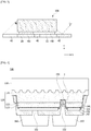
FIG. 5 is a conceptual diagram of a semiconductor device package according to another embodiment of the present invention, andFIG. 6 is a diagram for describing a method of manufacturing the semiconductor device package according to another embodiment of the present invention. - The package according to the present embodiment may have a directivity angle that is greater than that of the existing semiconductor device package. For example, the semiconductor device package of
FIG. 1 may have a directivity angle in a range of 123 degrees to 130 degrees and a light flux of 178 lm. Therefore, it is necessary to control the directivity angle so as to increase the light flux. - The light emitting device package according to the present embodiment may include a
dam portion 41 which surrounds thelight emitting device 100. Thedam portion 41 may have a structure connected to thereflective layer 40, but the present invention is not limited thereto. Thedam portion 41 may be disposed on theedge portion 23 of thefirst lead frame 20. - The
dam portion 41 may have a composition that is identical to that of thereflective layer 40. For example, thedam portion 41 may have a structure in which reflective particles are dispersed in a base material. The base material may be one or more among a light-transmitting epoxy resin, a silicone resin, a polyimide resin, a urea resin, and an acrylic resin. For example, the polymer resin may be a silicone resin. The reflective particles may include particles such as TiO2 or SiO2. - The
dam portion 41 may be disposed in theflat portion 61 of thelens 60. A height of thedam portion 41 may be 1/3 times to two times a height of a semiconductor device. That is, the height of thedam portion 41 may be variously adjusted to control the directivity angle. However, it may be advantageous in terms of reliability that the height of thedam portion 41 is formed to be lower than that of theflat portion 61. - The
dam portion 41 may include afirst surface 41a close to thelight emitting device 100, and asecond surface 41b opposite to thefirst surface 41a. Thefirst surface 41a may have a curvature, whereas thesecond surface 41b may have a flat surface. When thefirst surface 41a has a curvature, the light emitted from thelight emitting device 100 may be effectively reflected upward. When thedam portion 41 is formed, the directivity angle is controlled in a range of 120 degrees to 127 degrees, and the light flux is improved to 182 lm. - Referring to
FIG. 6 , thedam portion 41 may be formed on theedge portion 23. A cross section of thedam portion 41 may be formed in a semicircular shape. Thedam portion 41 and thereflective layer 40 may be formed simultaneously, and alternatively, thereflective layer 40 may be formed and then thedam portion 41 may be formed thereon. Thereafter, a portion C1 of the edge of thesubstrate 10 may be cut. - Then, using a dispenser, a resin which forms the lens may be applied. In this case, the
dam portion 41 may be pre-cured to maintain a shape thereof, and then thelens 60 and thedam portion 41 may be cured simultaneously. However, the present invention is not particularly limited thereto, and thedam portion 41 may be manufactured through a separate process and attached via an adhesive. -
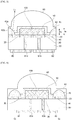
FIG. 7 is a conceptual diagram of a semiconductor device package according to still another embodiment of the present invention, andFIG. 8 is a diagram illustrating a modified example ofFIG. 7 . - Referring to
FIG. 7 , in the above-described structure, a wavelength conversion layer may be formed on an entire upper surface by being applied through spraying. In the present embodiment, awavelength conversion layer 51 may be manufactured in the form of a film and disposed on thelight emitting device 100. When thewavelength conversion layer 51 is manufactured in the form of a film, there is an advantage in that the package can be easily manufactured and entirely uniform light can be implemented. - A
reflective layer 42 may be disposed to the side surface of thelight emitting device 100. Thereflective layer 42 may be disposed such that a thickness thereof decreases farther away from the side surface of thelight emitting device 100. In this case, although an inclined surface is shown as a straight line, the inclined surface may have a concave curvature due to gravity during formation of the reflective layer. - The
edge portion 23 of thefirst lead frame 20 may prevent thereflective layer 42 from flowing downward to the outside of thesubstrate 10. With the above-described configuration, thereflective layer 40 may reflect light emitted to the side surface of thelight emitting device 100 to increase the light extraction efficiency and effectively control the directivity angle. - Referring to
FIG. 8 , adam portion 41 may be further disposed on theedge portion 23. Thedam portion 41 may be manufactured in the same manner as in the manufacturing process described with reference toFIG. 6 . According to the present embodiment, the directivity angle may be controlled by thedam portion 41 and thereflective layer 40 such that the light flux may be improved. - The
dam portion 41 may have a composition that is identical to that of thereflective layer 42. For example, thedam portion 41 may have a structure in which reflective particles are dispersed in a base material. The base material may be one or more among a light-transmitting epoxy resin, a silicone resin, a polyimide resin, a urea resin, and an acrylic resin. For example, the polymer resin may be a silicone resin. The reflective particles may include particles such as TiO2 or SiO2. - The
dam portion 41 may be disposed in theflat portion 61 of thelens 60. A height of thedam portion 41 may be 1/3 times to two times a height of a semiconductor device. That is, the height of thedam portion 41 may be variously adjusted to control the directivity angle. However, it may be advantageous in terms of reliability that the height of thedam portion 41 is formed to be lower than that of theflat portion 61. - The
dam portion 41 may include a first surface close to thelight emitting device 100 and a second surface opposite to the first surface. The first surface may have a curvature, whereas the second surface may have a flat surface. When the first surface has a curvature, the light emitted from thelight emitting device 100 may be effectively reflected upward. - The above-described semiconductor device package according to the embodiments of the present invention may further include an optical member such as a light guiding panel, a prism sheet, and a diffusion sheet, thereby serving as a backlight unit. Further, the semiconductor device package according to the embodiments of the present invention may be further applied to a display device, a lighting device, and an indicating device.
- At this point, the display device may include a bottom cover, a reflector, a light-emitting module, a light guide plate, an optical sheet, a display panel, an image signal output circuit, and a color filter. The bottom cover, the reflector, the light-emitting module, the light guide plate, and the optical sheet may configure a backlight unit.
- The reflector is disposed on the bottom cover, and the light-emitting module emits light. The light guiding panel is disposed in front of the reflector to guide the light emitted from the light emitting device forward, and the optical sheet may include a prism sheet or the like to be disposed in front of the light guiding panel. The display panel is disposed in front of the optical sheet, the image signal output circuit supplies an image signal to the display panel, and the color filter is disposed in front of the display panel.
- Further, the lighting device may include a light source module having a substrate and the semiconductor device package of the embodiments, a heat dissipation part configured to dissipate heat of the light source module, and a power supplier configured to process or convert an electrical signal provided from the outside to provide the electrical signal to the light source module. Further, the lighting device may include a lamp, a head lamp, a street lamp, or the like.
- It should be understood that the present invention is not limited to the above described embodiments and the accompanying drawings, and various substitutions, modifications, and alterations can be devised by those skilled in the art to which the present invention pertains without departing from the technical spirit of the embodiments described herein.
Claims (10)
- A semiconductor device package comprising:a substrate;a first lead frame and a second lead frame disposed on the substrate;a light emitting device electrically connected to the first and second lead frames;a reflective layer disposed on the substrate and configured to reflect light emitted from the light emitting device; anda lens disposed on the substrate and configured to cover the light emitting device, the reflective layer, the first and second lead frames,wherein the first lead frame includes:a first lead electrode portion electrically connected to the light emitting device;an edge portion disposed on an edge of the substrate; andan extension configured to connect the edge portion to the first lead electrode portion, andthe reflective layer is disposed inside the edge portion.
- The semiconductor device package of claim 1, comprising:a first pad electrically connected to the first lead frame;a second pad electrically connected to the second lead frame;a first through electrode configured to pass through the substrate in a thickness direction thereof to electrically connect the first lead frame to the first pad; anda second through electrode configured to pass through the substrate in the thickness direction thereof to electrically connect the second lead frame to the second pad.
- The semiconductor device package of claim 1, wherein a lead electrode portion of each of the first and second lead frames is connected to an electrode pad for a Zener diode.
- The semiconductor device package of claim 1, wherein the edge portion surrounds a second lead electrode portion of the second lead frame.
- The semiconductor device package of claim 1, wherein the lens includes a convex portion disposed on a central portion of the lens and a flat portion configured to surround the convex portion.
- The semiconductor device package of claim 5, comprising a dam portion disposed between the substrate and the flat portion,
wherein the dam portion has one surface close to the light emitting device and the other surface opposite to the one surface, and
the one surface has a curvature and the other surface has a flat surface. - The semiconductor device package of claim 6, wherein the dam portion is connected to the reflective layer.
- The semiconductor device package of claim 1, wherein the reflective layer covers a side surface of the light emitting device.
- The semiconductor device package of claim 8, wherein a thickness of the reflective layer decreases farther away from the light emitting device.
- The semiconductor device package of claim 1, comprising a wavelength conversion layer disposed on the light emitting device,
wherein the wavelength conversion layer extends to the reflective layer.
Applications Claiming Priority (2)
| Application Number | Priority Date | Filing Date | Title |
|---|---|---|---|
| KR1020160141323A KR102709497B1 (en) | 2016-10-27 | 2016-10-27 | Semiconductor device package |
| PCT/KR2017/011979 WO2018080224A1 (en) | 2016-10-27 | 2017-10-27 | Semiconductor device package |
Publications (3)
| Publication Number | Publication Date |
|---|---|
| EP3534413A1 true EP3534413A1 (en) | 2019-09-04 |
| EP3534413A4 EP3534413A4 (en) | 2020-06-24 |
| EP3534413B1 EP3534413B1 (en) | 2023-12-13 |
Family
ID=62025195
Family Applications (1)
| Application Number | Title | Priority Date | Filing Date |
|---|---|---|---|
| EP17864168.4A Active EP3534413B1 (en) | 2016-10-27 | 2017-10-27 | Semiconductor device package |
Country Status (5)
| Country | Link |
|---|---|
| US (1) | US10686108B2 (en) |
| EP (1) | EP3534413B1 (en) |
| KR (1) | KR102709497B1 (en) |
| CN (1) | CN109923684A (en) |
| WO (1) | WO2018080224A1 (en) |
Cited By (1)
| Publication number | Priority date | Publication date | Assignee | Title |
|---|---|---|---|---|
| WO2023046655A1 (en) * | 2021-09-23 | 2023-03-30 | Osram Opto Semiconductors Gmbh | Optical elements, radiation-emitting semiconductor component and methods for producing same |
Families Citing this family (14)
| Publication number | Priority date | Publication date | Assignee | Title |
|---|---|---|---|---|
| HUE025477T2 (en) | 2008-04-30 | 2016-02-29 | Xyleco Inc | Processing biomass |
| US7867358B2 (en) | 2008-04-30 | 2011-01-11 | Xyleco, Inc. | Paper products and methods and systems for manufacturing such products |
| US8236535B2 (en) | 2008-04-30 | 2012-08-07 | Xyleco, Inc. | Processing biomass |
| US8212087B2 (en) | 2008-04-30 | 2012-07-03 | Xyleco, Inc. | Processing biomass |
| US9266053B2 (en) | 2012-06-18 | 2016-02-23 | Invacare Corporation | System and method for concentrating gas |
| US9061238B2 (en) | 2013-03-15 | 2015-06-23 | Invacare Corporation | Gas concentrator |
| KR102408974B1 (en) | 2017-11-23 | 2022-06-15 | 삼성디스플레이 주식회사 | Display device and method of manufacturing the same |
| JP7054005B2 (en) * | 2018-09-28 | 2022-04-13 | 日亜化学工業株式会社 | Light emitting device |
| CN109585633A (en) * | 2018-10-12 | 2019-04-05 | 华中科技大学鄂州工业技术研究院 | A kind of LED encapsulation structure and LED component |
| KR102827371B1 (en) * | 2019-10-01 | 2025-07-01 | 엘지전자 주식회사 | Display device using micro led and manufacturing method thereof |
| US11950438B2 (en) * | 2019-12-17 | 2024-04-02 | Lg Display Co., Ltd. | Inorganic light emitting diode and inorganic light emitting device including the same |
| CN114122241B (en) * | 2022-01-28 | 2022-05-13 | 江西鸿利光电有限公司 | Light emitting device and method of manufacturing the same |
| US20240120452A1 (en) * | 2022-10-11 | 2024-04-11 | Creeled, Inc. | Reflectors for support structures in light-emitting diode packages |
| US20240363815A1 (en) * | 2023-04-25 | 2024-10-31 | Seoul Semiconductor Co., Ltd. | Light emitting device |
Family Cites Families (14)
| Publication number | Priority date | Publication date | Assignee | Title |
|---|---|---|---|---|
| US20030075724A1 (en) * | 2001-10-19 | 2003-04-24 | Bily Wang | Wing-shaped surface mount package for light emitting diodes |
| US20050189626A1 (en) * | 2004-01-29 | 2005-09-01 | Tan Xiaochun | Semiconductor device support structures |
| WO2006016398A1 (en) * | 2004-08-10 | 2006-02-16 | Renesas Technology Corp. | Light emitting device and process for manufacturing the same |
| DE112006000694B4 (en) | 2005-03-24 | 2013-10-17 | Kyocera Corp. | Housing for light emitting device, light emitting device and lighting device |
| US20070290220A1 (en) * | 2006-06-20 | 2007-12-20 | Bily Wang | Package for a light emitting diode and a process for fabricating the same |
| KR20080060114A (en) | 2006-12-26 | 2008-07-01 | 엘지이노텍 주식회사 | Light emitting diode package and manufacturing method thereof, surface light emitting device |
| KR101406787B1 (en) | 2008-06-24 | 2014-06-12 | 삼성전자주식회사 | LED package |
| EP3547380B1 (en) * | 2010-02-09 | 2023-12-20 | Nichia Corporation | Light emitting device |
| JP6038443B2 (en) | 2011-11-21 | 2016-12-07 | スタンレー電気株式会社 | Semiconductor light emitting device and method for manufacturing semiconductor light emitting device |
| KR101973613B1 (en) * | 2012-09-13 | 2019-04-29 | 엘지이노텍 주식회사 | Light emitting device and lighting system |
| KR20140102563A (en) * | 2013-02-14 | 2014-08-22 | 삼성전자주식회사 | Light-emitting device packages |
| JP6484396B2 (en) | 2013-06-28 | 2019-03-13 | 日亜化学工業株式会社 | Light emitting device package and light emitting device using the same |
| WO2015068072A1 (en) * | 2013-11-07 | 2015-05-14 | Koninklijke Philips N.V. | Substrate for led with total-internal reflection layer surrounding led |
| KR102122361B1 (en) * | 2013-12-27 | 2020-06-15 | 삼성전자주식회사 | Flip-chip Light Emitting Device package substrate and Light Emitting Device package structure |
-
2016
- 2016-10-27 KR KR1020160141323A patent/KR102709497B1/en active Active
-
2017
- 2017-10-27 WO PCT/KR2017/011979 patent/WO2018080224A1/en not_active Ceased
- 2017-10-27 US US16/345,186 patent/US10686108B2/en active Active
- 2017-10-27 EP EP17864168.4A patent/EP3534413B1/en active Active
- 2017-10-27 CN CN201780066917.3A patent/CN109923684A/en active Pending
Cited By (1)
| Publication number | Priority date | Publication date | Assignee | Title |
|---|---|---|---|---|
| WO2023046655A1 (en) * | 2021-09-23 | 2023-03-30 | Osram Opto Semiconductors Gmbh | Optical elements, radiation-emitting semiconductor component and methods for producing same |
Also Published As
| Publication number | Publication date |
|---|---|
| KR20180046274A (en) | 2018-05-08 |
| US10686108B2 (en) | 2020-06-16 |
| KR102709497B1 (en) | 2024-09-26 |
| CN109923684A (en) | 2019-06-21 |
| US20190288168A1 (en) | 2019-09-19 |
| EP3534413A4 (en) | 2020-06-24 |
| EP3534413B1 (en) | 2023-12-13 |
| WO2018080224A1 (en) | 2018-05-03 |
Similar Documents
| Publication | Publication Date | Title |
|---|---|---|
| EP3534413B1 (en) | Semiconductor device package | |
| EP2432036B1 (en) | Light emitting diode | |
| KR101039879B1 (en) | Light emitting device and manufacturing method | |
| US10217918B2 (en) | Light-emitting element package | |
| KR102038443B1 (en) | Light emitting device and light emitting device package | |
| CN102222741B (en) | Light emitting device and light emitting device package | |
| KR101916131B1 (en) | Light emitting device, method for fabricating the same and lighting system | |
| KR102407329B1 (en) | Light source module and lighting apparatus | |
| EP2381489B1 (en) | Light emitting device, light emitting device package, and lighting system | |
| CN103972348B (en) | Luminescent device | |
| CN108040503B (en) | Light emitting device | |
| US8502248B2 (en) | Light emitting device, having protrusions from a conductive support member, lighting emitting device package, and lighting system | |
| US9117975B2 (en) | Light emitting device having an anti-crack layer | |
| US8994058B2 (en) | Light emitting device having an ohmic layer with a plurality of protruding contact portions | |
| US10270006B2 (en) | Light emitting device and light emitting module | |
| KR101734541B1 (en) | Light emitting device, light emitting device package | |
| KR102251225B1 (en) | Light source module | |
| KR20140097899A (en) | Light emitting device | |
| KR20130088556A (en) | Light emitting device and light emitting device package | |
| US10297716B2 (en) | Light emitting device and light emitting module | |
| KR20130005589A (en) | Light emitting device, light emitting device package, light unit, and method of fabricating light emitting device | |
| KR20150015983A (en) | Light emitting device | |
| KR20190038020A (en) | Semiconductor device package |
Legal Events
| Date | Code | Title | Description |
|---|---|---|---|
| STAA | Information on the status of an ep patent application or granted ep patent |
Free format text: STATUS: THE INTERNATIONAL PUBLICATION HAS BEEN MADE |
|
| PUAI | Public reference made under article 153(3) epc to a published international application that has entered the european phase |
Free format text: ORIGINAL CODE: 0009012 |
|
| STAA | Information on the status of an ep patent application or granted ep patent |
Free format text: STATUS: REQUEST FOR EXAMINATION WAS MADE |
|
| 17P | Request for examination filed |
Effective date: 20190426 |
|
| AK | Designated contracting states |
Kind code of ref document: A1 Designated state(s): AL AT BE BG CH CY CZ DE DK EE ES FI FR GB GR HR HU IE IS IT LI LT LU LV MC MK MT NL NO PL PT RO RS SE SI SK SM TR |
|
| AX | Request for extension of the european patent |
Extension state: BA ME |
|
| DAV | Request for validation of the european patent (deleted) | ||
| DAX | Request for extension of the european patent (deleted) | ||
| A4 | Supplementary search report drawn up and despatched |
Effective date: 20200526 |
|
| RIC1 | Information provided on ipc code assigned before grant |
Ipc: H01L 25/16 20060101ALN20200518BHEP Ipc: H01L 33/50 20100101ALN20200518BHEP Ipc: H01L 33/60 20100101ALI20200518BHEP Ipc: H01L 33/48 20100101AFI20200518BHEP Ipc: H01L 33/62 20100101ALI20200518BHEP Ipc: H01L 33/54 20100101ALN20200518BHEP |
|
| RAP1 | Party data changed (applicant data changed or rights of an application transferred) |
Owner name: SUZHOU LEKIN SEMICONDUCTOR CO., LTD. |
|
| STAA | Information on the status of an ep patent application or granted ep patent |
Free format text: STATUS: EXAMINATION IS IN PROGRESS |
|
| 17Q | First examination report despatched |
Effective date: 20220511 |
|
| GRAP | Despatch of communication of intention to grant a patent |
Free format text: ORIGINAL CODE: EPIDOSNIGR1 |
|
| STAA | Information on the status of an ep patent application or granted ep patent |
Free format text: STATUS: GRANT OF PATENT IS INTENDED |
|
| INTG | Intention to grant announced |
Effective date: 20230526 |
|
| GRAS | Grant fee paid |
Free format text: ORIGINAL CODE: EPIDOSNIGR3 |
|
| GRAA | (expected) grant |
Free format text: ORIGINAL CODE: 0009210 |
|
| STAA | Information on the status of an ep patent application or granted ep patent |
Free format text: STATUS: THE PATENT HAS BEEN GRANTED |
|
| AK | Designated contracting states |
Kind code of ref document: B1 Designated state(s): AL AT BE BG CH CY CZ DE DK EE ES FI FR GB GR HR HU IE IS IT LI LT LU LV MC MK MT NL NO PL PT RO RS SE SI SK SM TR |
|
| REG | Reference to a national code |
Ref country code: GB Ref legal event code: FG4D |
|
| REG | Reference to a national code |
Ref country code: CH Ref legal event code: EP |
|
| REG | Reference to a national code |
Ref country code: DE Ref legal event code: R096 Ref document number: 602017077557 Country of ref document: DE |
|
| REG | Reference to a national code |
Ref country code: IE Ref legal event code: FG4D |
|
| PG25 | Lapsed in a contracting state [announced via postgrant information from national office to epo] |
Ref country code: GR Free format text: LAPSE BECAUSE OF FAILURE TO SUBMIT A TRANSLATION OF THE DESCRIPTION OR TO PAY THE FEE WITHIN THE PRESCRIBED TIME-LIMIT Effective date: 20240314 |
|
| REG | Reference to a national code |
Ref country code: LT Ref legal event code: MG9D |
|
| PG25 | Lapsed in a contracting state [announced via postgrant information from national office to epo] |
Ref country code: LT Free format text: LAPSE BECAUSE OF FAILURE TO SUBMIT A TRANSLATION OF THE DESCRIPTION OR TO PAY THE FEE WITHIN THE PRESCRIBED TIME-LIMIT Effective date: 20231213 |
|
| REG | Reference to a national code |
Ref country code: NL Ref legal event code: MP Effective date: 20231213 |
|
| PG25 | Lapsed in a contracting state [announced via postgrant information from national office to epo] |
Ref country code: ES Free format text: LAPSE BECAUSE OF FAILURE TO SUBMIT A TRANSLATION OF THE DESCRIPTION OR TO PAY THE FEE WITHIN THE PRESCRIBED TIME-LIMIT Effective date: 20231213 |
|
| PG25 | Lapsed in a contracting state [announced via postgrant information from national office to epo] |
Ref country code: LT Free format text: LAPSE BECAUSE OF FAILURE TO SUBMIT A TRANSLATION OF THE DESCRIPTION OR TO PAY THE FEE WITHIN THE PRESCRIBED TIME-LIMIT Effective date: 20231213 Ref country code: GR Free format text: LAPSE BECAUSE OF FAILURE TO SUBMIT A TRANSLATION OF THE DESCRIPTION OR TO PAY THE FEE WITHIN THE PRESCRIBED TIME-LIMIT Effective date: 20240314 Ref country code: ES Free format text: LAPSE BECAUSE OF FAILURE TO SUBMIT A TRANSLATION OF THE DESCRIPTION OR TO PAY THE FEE WITHIN THE PRESCRIBED TIME-LIMIT Effective date: 20231213 Ref country code: BG Free format text: LAPSE BECAUSE OF FAILURE TO SUBMIT A TRANSLATION OF THE DESCRIPTION OR TO PAY THE FEE WITHIN THE PRESCRIBED TIME-LIMIT Effective date: 20240313 |
|
| REG | Reference to a national code |
Ref country code: AT Ref legal event code: MK05 Ref document number: 1641225 Country of ref document: AT Kind code of ref document: T Effective date: 20231213 |
|
| PG25 | Lapsed in a contracting state [announced via postgrant information from national office to epo] |
Ref country code: NL Free format text: LAPSE BECAUSE OF FAILURE TO SUBMIT A TRANSLATION OF THE DESCRIPTION OR TO PAY THE FEE WITHIN THE PRESCRIBED TIME-LIMIT Effective date: 20231213 |
|
| PG25 | Lapsed in a contracting state [announced via postgrant information from national office to epo] |
Ref country code: SE Free format text: LAPSE BECAUSE OF FAILURE TO SUBMIT A TRANSLATION OF THE DESCRIPTION OR TO PAY THE FEE WITHIN THE PRESCRIBED TIME-LIMIT Effective date: 20231213 Ref country code: RS Free format text: LAPSE BECAUSE OF FAILURE TO SUBMIT A TRANSLATION OF THE DESCRIPTION OR TO PAY THE FEE WITHIN THE PRESCRIBED TIME-LIMIT Effective date: 20231213 Ref country code: NO Free format text: LAPSE BECAUSE OF FAILURE TO SUBMIT A TRANSLATION OF THE DESCRIPTION OR TO PAY THE FEE WITHIN THE PRESCRIBED TIME-LIMIT Effective date: 20240313 Ref country code: NL Free format text: LAPSE BECAUSE OF FAILURE TO SUBMIT A TRANSLATION OF THE DESCRIPTION OR TO PAY THE FEE WITHIN THE PRESCRIBED TIME-LIMIT Effective date: 20231213 Ref country code: LV Free format text: LAPSE BECAUSE OF FAILURE TO SUBMIT A TRANSLATION OF THE DESCRIPTION OR TO PAY THE FEE WITHIN THE PRESCRIBED TIME-LIMIT Effective date: 20231213 Ref country code: HR Free format text: LAPSE BECAUSE OF FAILURE TO SUBMIT A TRANSLATION OF THE DESCRIPTION OR TO PAY THE FEE WITHIN THE PRESCRIBED TIME-LIMIT Effective date: 20231213 |
|
| PG25 | Lapsed in a contracting state [announced via postgrant information from national office to epo] |
Ref country code: IS Free format text: LAPSE BECAUSE OF FAILURE TO SUBMIT A TRANSLATION OF THE DESCRIPTION OR TO PAY THE FEE WITHIN THE PRESCRIBED TIME-LIMIT Effective date: 20240413 |
|
| PG25 | Lapsed in a contracting state [announced via postgrant information from national office to epo] |
Ref country code: AT Free format text: LAPSE BECAUSE OF FAILURE TO SUBMIT A TRANSLATION OF THE DESCRIPTION OR TO PAY THE FEE WITHIN THE PRESCRIBED TIME-LIMIT Effective date: 20231213 Ref country code: CZ Free format text: LAPSE BECAUSE OF FAILURE TO SUBMIT A TRANSLATION OF THE DESCRIPTION OR TO PAY THE FEE WITHIN THE PRESCRIBED TIME-LIMIT Effective date: 20231213 |
|
| PG25 | Lapsed in a contracting state [announced via postgrant information from national office to epo] |
Ref country code: SK Free format text: LAPSE BECAUSE OF FAILURE TO SUBMIT A TRANSLATION OF THE DESCRIPTION OR TO PAY THE FEE WITHIN THE PRESCRIBED TIME-LIMIT Effective date: 20231213 |
|
| PG25 | Lapsed in a contracting state [announced via postgrant information from national office to epo] |
Ref country code: SM Free format text: LAPSE BECAUSE OF FAILURE TO SUBMIT A TRANSLATION OF THE DESCRIPTION OR TO PAY THE FEE WITHIN THE PRESCRIBED TIME-LIMIT Effective date: 20231213 Ref country code: SK Free format text: LAPSE BECAUSE OF FAILURE TO SUBMIT A TRANSLATION OF THE DESCRIPTION OR TO PAY THE FEE WITHIN THE PRESCRIBED TIME-LIMIT Effective date: 20231213 Ref country code: RO Free format text: LAPSE BECAUSE OF FAILURE TO SUBMIT A TRANSLATION OF THE DESCRIPTION OR TO PAY THE FEE WITHIN THE PRESCRIBED TIME-LIMIT Effective date: 20231213 Ref country code: IT Free format text: LAPSE BECAUSE OF FAILURE TO SUBMIT A TRANSLATION OF THE DESCRIPTION OR TO PAY THE FEE WITHIN THE PRESCRIBED TIME-LIMIT Effective date: 20231213 Ref country code: IS Free format text: LAPSE BECAUSE OF FAILURE TO SUBMIT A TRANSLATION OF THE DESCRIPTION OR TO PAY THE FEE WITHIN THE PRESCRIBED TIME-LIMIT Effective date: 20240413 Ref country code: EE Free format text: LAPSE BECAUSE OF FAILURE TO SUBMIT A TRANSLATION OF THE DESCRIPTION OR TO PAY THE FEE WITHIN THE PRESCRIBED TIME-LIMIT Effective date: 20231213 Ref country code: CZ Free format text: LAPSE BECAUSE OF FAILURE TO SUBMIT A TRANSLATION OF THE DESCRIPTION OR TO PAY THE FEE WITHIN THE PRESCRIBED TIME-LIMIT Effective date: 20231213 Ref country code: AT Free format text: LAPSE BECAUSE OF FAILURE TO SUBMIT A TRANSLATION OF THE DESCRIPTION OR TO PAY THE FEE WITHIN THE PRESCRIBED TIME-LIMIT Effective date: 20231213 |
|
| PG25 | Lapsed in a contracting state [announced via postgrant information from national office to epo] |
Ref country code: PL Free format text: LAPSE BECAUSE OF FAILURE TO SUBMIT A TRANSLATION OF THE DESCRIPTION OR TO PAY THE FEE WITHIN THE PRESCRIBED TIME-LIMIT Effective date: 20231213 Ref country code: PT Free format text: LAPSE BECAUSE OF FAILURE TO SUBMIT A TRANSLATION OF THE DESCRIPTION OR TO PAY THE FEE WITHIN THE PRESCRIBED TIME-LIMIT Effective date: 20240415 |
|
| PG25 | Lapsed in a contracting state [announced via postgrant information from national office to epo] |
Ref country code: PT Free format text: LAPSE BECAUSE OF FAILURE TO SUBMIT A TRANSLATION OF THE DESCRIPTION OR TO PAY THE FEE WITHIN THE PRESCRIBED TIME-LIMIT Effective date: 20240415 Ref country code: PL Free format text: LAPSE BECAUSE OF FAILURE TO SUBMIT A TRANSLATION OF THE DESCRIPTION OR TO PAY THE FEE WITHIN THE PRESCRIBED TIME-LIMIT Effective date: 20231213 |
|
| REG | Reference to a national code |
Ref country code: DE Ref legal event code: R097 Ref document number: 602017077557 Country of ref document: DE |
|
| PG25 | Lapsed in a contracting state [announced via postgrant information from national office to epo] |
Ref country code: DK Free format text: LAPSE BECAUSE OF FAILURE TO SUBMIT A TRANSLATION OF THE DESCRIPTION OR TO PAY THE FEE WITHIN THE PRESCRIBED TIME-LIMIT Effective date: 20231213 |
|
| PLBE | No opposition filed within time limit |
Free format text: ORIGINAL CODE: 0009261 |
|
| STAA | Information on the status of an ep patent application or granted ep patent |
Free format text: STATUS: NO OPPOSITION FILED WITHIN TIME LIMIT |
|
| PG25 | Lapsed in a contracting state [announced via postgrant information from national office to epo] |
Ref country code: SI Free format text: LAPSE BECAUSE OF FAILURE TO SUBMIT A TRANSLATION OF THE DESCRIPTION OR TO PAY THE FEE WITHIN THE PRESCRIBED TIME-LIMIT Effective date: 20231213 |
|
| PG25 | Lapsed in a contracting state [announced via postgrant information from national office to epo] |
Ref country code: SI Free format text: LAPSE BECAUSE OF FAILURE TO SUBMIT A TRANSLATION OF THE DESCRIPTION OR TO PAY THE FEE WITHIN THE PRESCRIBED TIME-LIMIT Effective date: 20231213 Ref country code: DK Free format text: LAPSE BECAUSE OF FAILURE TO SUBMIT A TRANSLATION OF THE DESCRIPTION OR TO PAY THE FEE WITHIN THE PRESCRIBED TIME-LIMIT Effective date: 20231213 |
|
| 26N | No opposition filed |
Effective date: 20240916 |
|
| REG | Reference to a national code |
Ref country code: DE Ref legal event code: R079 Ref document number: 602017077557 Country of ref document: DE Free format text: PREVIOUS MAIN CLASS: H01L0033480000 Ipc: H10H0020850000 |
|
| REG | Reference to a national code |
Ref country code: CH Ref legal event code: PL |
|
| GBPC | Gb: european patent ceased through non-payment of renewal fee |
Effective date: 20241027 |
|
| PG25 | Lapsed in a contracting state [announced via postgrant information from national office to epo] |
Ref country code: MC Free format text: LAPSE BECAUSE OF FAILURE TO SUBMIT A TRANSLATION OF THE DESCRIPTION OR TO PAY THE FEE WITHIN THE PRESCRIBED TIME-LIMIT Effective date: 20231213 |
|
| PG25 | Lapsed in a contracting state [announced via postgrant information from national office to epo] |
Ref country code: GB Free format text: LAPSE BECAUSE OF NON-PAYMENT OF DUE FEES Effective date: 20241027 |
|
| PG25 | Lapsed in a contracting state [announced via postgrant information from national office to epo] |
Ref country code: BE Free format text: LAPSE BECAUSE OF NON-PAYMENT OF DUE FEES Effective date: 20241031 Ref country code: LU Free format text: LAPSE BECAUSE OF NON-PAYMENT OF DUE FEES Effective date: 20241027 |
|
| PG25 | Lapsed in a contracting state [announced via postgrant information from national office to epo] |
Ref country code: FR Free format text: LAPSE BECAUSE OF NON-PAYMENT OF DUE FEES Effective date: 20241031 |
|
| PG25 | Lapsed in a contracting state [announced via postgrant information from national office to epo] |
Ref country code: CH Free format text: LAPSE BECAUSE OF NON-PAYMENT OF DUE FEES Effective date: 20241031 |
|
| REG | Reference to a national code |
Ref country code: BE Ref legal event code: MM Effective date: 20241031 |
|
| PG25 | Lapsed in a contracting state [announced via postgrant information from national office to epo] |
Ref country code: FI Free format text: LAPSE BECAUSE OF FAILURE TO SUBMIT A TRANSLATION OF THE DESCRIPTION OR TO PAY THE FEE WITHIN THE PRESCRIBED TIME-LIMIT Effective date: 20231213 |
|
| PG25 | Lapsed in a contracting state [announced via postgrant information from national office to epo] |
Ref country code: IE Free format text: LAPSE BECAUSE OF NON-PAYMENT OF DUE FEES Effective date: 20241027 |
|
| PGFP | Annual fee paid to national office [announced via postgrant information from national office to epo] |
Ref country code: DE Payment date: 20250910 Year of fee payment: 9 |
|
| PG25 | Lapsed in a contracting state [announced via postgrant information from national office to epo] |
Ref country code: CY Free format text: LAPSE BECAUSE OF FAILURE TO SUBMIT A TRANSLATION OF THE DESCRIPTION OR TO PAY THE FEE WITHIN THE PRESCRIBED TIME-LIMIT; INVALID AB INITIO Effective date: 20171027 |
|
| PG25 | Lapsed in a contracting state [announced via postgrant information from national office to epo] |
Ref country code: HU Free format text: LAPSE BECAUSE OF FAILURE TO SUBMIT A TRANSLATION OF THE DESCRIPTION OR TO PAY THE FEE WITHIN THE PRESCRIBED TIME-LIMIT; INVALID AB INITIO Effective date: 20171027 |