EP3534397A1 - Resin-sealed semiconductor device - Google Patents
Resin-sealed semiconductor device Download PDFInfo
- Publication number
- EP3534397A1 EP3534397A1 EP17865648.4A EP17865648A EP3534397A1 EP 3534397 A1 EP3534397 A1 EP 3534397A1 EP 17865648 A EP17865648 A EP 17865648A EP 3534397 A1 EP3534397 A1 EP 3534397A1
- Authority
- EP
- European Patent Office
- Prior art keywords
- resin
- sealing portion
- semiconductor device
- resin sealing
- power
- Prior art date
- Legal status (The legal status is an assumption and is not a legal conclusion. Google has not performed a legal analysis and makes no representation as to the accuracy of the status listed.)
- Granted
Links
Images


Classifications
-
- H—ELECTRICITY
- H10—SEMICONDUCTOR DEVICES; ELECTRIC SOLID-STATE DEVICES NOT OTHERWISE PROVIDED FOR
- H10W—GENERIC PACKAGES, INTERCONNECTIONS, CONNECTORS OR OTHER CONSTRUCTIONAL DETAILS OF DEVICES COVERED BY CLASS H10
- H10W42/00—Arrangements for protection of devices
- H10W42/80—Arrangements for protection of devices protecting against overcurrent or overload, e.g. fuses or shunts
-
- H—ELECTRICITY
- H10—SEMICONDUCTOR DEVICES; ELECTRIC SOLID-STATE DEVICES NOT OTHERWISE PROVIDED FOR
- H10W—GENERIC PACKAGES, INTERCONNECTIONS, CONNECTORS OR OTHER CONSTRUCTIONAL DETAILS OF DEVICES COVERED BY CLASS H10
- H10W74/00—Encapsulations, e.g. protective coatings
- H10W74/40—Encapsulations, e.g. protective coatings characterised by their materials
-
- H—ELECTRICITY
- H10—SEMICONDUCTOR DEVICES; ELECTRIC SOLID-STATE DEVICES NOT OTHERWISE PROVIDED FOR
- H10W—GENERIC PACKAGES, INTERCONNECTIONS, CONNECTORS OR OTHER CONSTRUCTIONAL DETAILS OF DEVICES COVERED BY CLASS H10
- H10W74/00—Encapsulations, e.g. protective coatings
- H10W74/10—Encapsulations, e.g. protective coatings characterised by their shape or disposition
- H10W74/111—Encapsulations, e.g. protective coatings characterised by their shape or disposition the semiconductor body being completely enclosed
-
- H—ELECTRICITY
- H10—SEMICONDUCTOR DEVICES; ELECTRIC SOLID-STATE DEVICES NOT OTHERWISE PROVIDED FOR
- H10W—GENERIC PACKAGES, INTERCONNECTIONS, CONNECTORS OR OTHER CONSTRUCTIONAL DETAILS OF DEVICES COVERED BY CLASS H10
- H10W90/00—Package configurations
- H10W90/701—Package configurations characterised by the relative positions of pads or connectors relative to package parts
- H10W90/731—Package configurations characterised by the relative positions of pads or connectors relative to package parts of die-attach connectors
- H10W90/736—Package configurations characterised by the relative positions of pads or connectors relative to package parts of die-attach connectors between a chip and a stacked lead frame, conducting package substrate or heat sink
-
- H—ELECTRICITY
- H10—SEMICONDUCTOR DEVICES; ELECTRIC SOLID-STATE DEVICES NOT OTHERWISE PROVIDED FOR
- H10W—GENERIC PACKAGES, INTERCONNECTIONS, CONNECTORS OR OTHER CONSTRUCTIONAL DETAILS OF DEVICES COVERED BY CLASS H10
- H10W90/00—Package configurations
- H10W90/701—Package configurations characterised by the relative positions of pads or connectors relative to package parts
- H10W90/751—Package configurations characterised by the relative positions of pads or connectors relative to package parts of bond wires
- H10W90/756—Package configurations characterised by the relative positions of pads or connectors relative to package parts of bond wires between a chip and a stacked lead frame, conducting package substrate or heat sink
Definitions
- the present invention relates to a resin-sealed semiconductor device to be applied to, for example, an automobile, and more particularly, to a resin-sealed semiconductor device in which a short-circuit current generated by a short-circuit fault of a component is cut off.
- An inverter device for motor drive which is configured to drive a motor, uses a battery as a power source to supply a high-voltage drive power to a motor drive circuit.
- a resin-sealed power semiconductor device is used in the inverter device for motor drive, and the importance of resin-sealed semiconductor devices as a key device is ever increasing in the field of power electronics.
- a power semiconductor element used in the inverter device for motor drive is sealed with resin along with other components.
- a short-circuit current flows in an excessive amount when a short-circuit fault occurs in a smoothing capacitor or other electronic parts of the power semiconductor element or of a snubber circuit while power is supplied from the battery.
- an overcurrent flows into the power semiconductor element and causes a short-circuit fault.
- an overcurrent flowing between the inverter device for motor drive and the battery can be blocked by a fuse for cutting off an overcurrent, which is inserted between the power semiconductor device and the battery.
- a chip-type overcurrent cutting fuse is very expensive.
- overcurrent cutting means that is simple but capable of cutting off a possible flow of overcurrent into the battery without fail when a short-circuit fault occurs in the power semiconductor element.
- One method of providing a resin-sealed semiconductor device having a fuse function uses a thin metal wire for joining the power semiconductor element to an external terminal as a fuse.
- the thin metal wire is melted by heat generated during a flow of an overcurrent, and eventually breaks as a result of the migration of the metal to the surrounding space.
- the thin metal wire is sealed with resin along with the power semiconductor element, there is no space to which the metal from the thin metal wire melted by a flow of an overcurrent can migrate, and the overcurrent accordingly continues to flow in the thin metal wire for a long period of time.
- the copper wire having the fuse function is partially covered with silicone gel in the semiconductor device described in Patent Literature 1.
- the silicone gel in contact with the copper wire is carbonized by heat generated in the copper wire, and, when the layer of the silicone gel is not thick enough, a problem occurs in which the product of the carbonization piles up and has a combustion reaction upon contact with the atmospheric air, thereby causing the resin-sealed semiconductor device to emit smoke and ignite.
- the present invention has been made to solve the problem described above, and an object of the present invention is to provide a resin-sealed semiconductor device capable of cutting off an overcurrent without fail and having high resistance against smoking and ignition.
- a resin-sealed semiconductor device which includes a power semiconductor element and a power lead connected to a main electrode of the power semiconductor element, the power semiconductor element being molded with resin, the power lead being protruded from a molded resin portion
- the resin-sealed semiconductor device including: a fuse portion formed in the power lead; a first resin sealing portion configured to cover the fuse portion; and a second resin sealing portion configured to block the first resin sealing portion from atmospheric air and to form the molded resin portion.
- the fuse portion formed in the power lead there are formed the fuse portion formed in the power lead, the first resin sealing portion configured to cover the fuse portion, and the second resin sealing portion configured to block the first resin sealing portion from atmospheric air and to form the molded resin portion.
- An overcurrent can be cut off without fail by forming the fuse portion in the power lead.
- smoking and ignition can be prevented by covering the fuse portion with the first resin sealing portion and blocking the first resin portion from the atmospheric air with the second resin sealing portion, and thereby suppressing the combustion reaction of the resin.
- FIG. 1 is a plan view for illustrating a resin-sealed semiconductor device according to a first embodiment of the present invention.
- FIG. 2 is a sectional view taken along the line A-A of FIG. 1 .
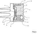
- FIG. 3 is a sectional view taken along the line B-B of FIG. 1 .
- a resin-sealed semiconductor device 100 includes an external terminal lead frame 1, which is a power lead, a power semiconductor element 2, a conductive joint material 3, control lead frames 4, a molded resin portion 5, which is a second resin sealing portion, a heat sink 6, a fuse portion 7, an insulating case 8, a first resin sealing portion 9, an insulating sheet 10, an external connection terminal 11, and an inner lead 12.
- the power semiconductor element 2 is formed on a face opposite to the heat sink 6.
- a main electrode of the power semiconductor element 2 is connected to the external terminal lead frame 1 by the joint material 3.
- the external terminal lead frame 1 is used for input and output, and is fixed to the heat sink 6 by the insulating sheet 10.
- the external terminal lead frame 1 is electrically connected, by welding or soldering, to the external connection terminal 11, which is inserted in the insulating case 8.
- the power semiconductor element 2 and the control lead frames 4 are electrically connected by the inner lead 12 or a bonding wire (not shown).
- the power semiconductor element 2 is constituted by a power field-effect transistor (power metal-oxide-semiconductor field-effect transistor: power MOSFET), an insulated gate bipolar transistor (IGBT), or the like.
- a power field-effect transistor power metal-oxide-semiconductor field-effect transistor: power MOSFET
- IGBT insulated gate bipolar transistor
- the above-mentioned elements are used in an inverter device configured to drive a motor or similar electric equipment to control a rated current of several hundred amperes.
- the conductive joint material 3 is made of solder or the like, and is used to electrically connect and firmly fix the power semiconductor element 2 to the external terminal lead frame 1.
- the fuse portion 7 is formed in the external terminal lead frame 1, and is embedded in the first resin sealing portion 9.
- the first resin sealing portion 9 is formed by application with the use of a dispenser or the like after the power semiconductor element 2 is mounted to the heat sink 6, and after the external terminal lead frame 1 and the external connection terminal 11 are joined. The mounting of a control substrate (not shown) and the cast molding of the molded resin portion 5 are then conducted.
- At least a surface of the first resin sealing portion 9 is required to be cured prior to the cast molding of the molded resin portion 5 because curing can be inhibited by accidental mixing of the first resin sealing portion 9 and the molded resin portion 5. It is therefore preferred for the first resin sealing portion 9 to be made of resin that is cured by moisture curing or solvent removal. Another material suitable for the first resin sealing portion 9 is rubber having an elastic coefficient of about several tens MPa, or a similar material, and silicone rubber or silicone gel from which an arc extinguishing effect can be expected is used.
- the fuse portion 7 is formed by forming a narrowed portion 7a in the external terminal lead frame 1, and is melted down to cut off the overcurrent when an overcurrent flows into the external terminal lead frame 1.
- the external terminal lead frame 1 can be formed, though not limited thereto, by performing punching process on a plate made of copper or a copper alloy and having a thickness of from about 0.5 mm to about 1 mm.
- the heat sink 6 and the insulating case 8 are arranged so as to wrap around the fuse portion 7, and have the role of molding the molded resin portion 5 by cast molding.
- a material having an elastic coefficient of several GPa for example, epoxy resin, is suitable for the molded resin portion 5.
- the molded resin portion 5 covers the first resin sealing portion 9 so as to expose a peripheral end portion of the external terminal lead frame 1.
- the insulating case 8 has a main body portion, an opening portion, and a hollow portion. Resin for cast molding is injected from the opening portion of the insulating case 8 to mold the molded resin portion 5 so that the insulating case 8 containing the power semiconductor element 2 and the first resin sealing portion 9 inside is entirely covered.
- the molded resin portion 5 is firmly fixed above the heat sink 6 made of metal, with the insulating sheet 10 interposed between the molded resin portion 5 and the heat sink 6.
- the insulating sheet 10 is inserted between the external terminal lead frame 1 and the heat sink 6 to firmly fix the external terminal lead frame 1 and the heat sink 6. Any material having high heat conductance and high electrical insulation properties, for example, a ceramic sheet, can be used for the insulating sheet 10.
- the molded resin portion 5 can be molded from any thermally curable resin material.
- An example of a preferred material from which the molded resin portion 5 is molded is epoxy resin in which alumina, a silicon compound, or other substance having high heat conductance is contained as a filler.
- the heat sink 6 has the role of dissipating heat that is generated when a current flows in the power semiconductor element 2 sealed in the molded resin portion 5.
- the heat sink 6 is formed from a material having a heat conductivity of 100 W/m ⁇ K or more, for example, aluminum.
- the molded resin portion 5 is joined directly to a top face of the heat sink 6, and a plurality of cooling fins 6a are arranged on a bottom face of the heat sink 6.
- an overcurrent is thus cut off without fail by forming the fuse portion 7 in the external terminal lead frame 1, and the resin-sealed semiconductor device can also be prevented from emitting smoke and igniting by covering the fuse portion 7 with the first resin sealing portion 9 and blocking the first resin sealing portion 9 from the atmospheric air, and thereby suppressing the combustion reaction of the resin.
- the molded resin portion 5 is formed from epoxy resin in which alumina, a silicon compound, or other substance having high heat conductance is contained as a filler, and is accordingly high in the conductance of heat to the first resin sealing portion 9, which means that heat generated in the fuse portion 7 can be conducted with efficiency to suppress the combustion reaction.
- the molded resin portion 5, which has a high elastic coefficient, is arranged around the first resin sealing portion 9, which has a low elastic coefficient, thereby preventing the molded resin portion 5 from developing a crack due to thermal stress applied when the fuse is melted down. This allows the spacing to be kept to a proper distance when the fuse is melted down, thereby ensuring that a current is cut off without fail.
- Substance of the fuse scattered by the melting down lands on the first resin sealing portion 9, which has a low elastic coefficient, and the amount of scattered substance that remains in the melted down portion of the fuse is accordingly small. A stable overcurrent cutting effect is obtained as a result.
- the scattered substance is also prevented from flying to the outside by arranging the molded resin portion 5, which has a high elastic coefficient, around the first resin sealing portion 9, which has a low elastic coefficient.
- the molded resin portion 5 is in direct contact with the top face of the heat sink 6, and the plurality of cooling fins 6a are formed on the bottom face of the heat sink 6. This reduces heat generation in the fuse portion 7 and accordingly suppresses the combustion reaction.
- the fuse portion formed in the power lead, the first resin sealing portion configured to cover the fuse portion, and the second resin sealing portion configured to block the first resin sealing portion from atmospheric air and to form the molded resin portion are formed.
- An overcurrent can be cut off without fail by forming the fuse portion in the power lead.
- smoking and ignition can be prevented by covering the fuse portion with the first resin sealing portion and covering the first resin portion with the second resin sealing portion to block the first resin portion from the atmospheric air, and thereby suppressing the combustion reaction of the resin.
Landscapes
- Structures Or Materials For Encapsulating Or Coating Semiconductor Devices Or Solid State Devices (AREA)
Abstract
Description
- The present invention relates to a resin-sealed semiconductor device to be applied to, for example, an automobile, and more particularly, to a resin-sealed semiconductor device in which a short-circuit current generated by a short-circuit fault of a component is cut off.
- In recent years, motor-driven vehicles such as hybrid automobiles and electric automobiles are actively being developed in the automotive industry. An inverter device for motor drive, which is configured to drive a motor, uses a battery as a power source to supply a high-voltage drive power to a motor drive circuit. A resin-sealed power semiconductor device is used in the inverter device for motor drive, and the importance of resin-sealed semiconductor devices as a key device is ever increasing in the field of power electronics.
- A power semiconductor element used in the inverter device for motor drive is sealed with resin along with other components. In this type of resin-sealed semiconductor device, a short-circuit current flows in an excessive amount when a short-circuit fault occurs in a smoothing capacitor or other electronic parts of the power semiconductor element or of a snubber circuit while power is supplied from the battery. For instance, when upper and lower arms of an inverter are short-circuited by malfunction of a gate drive circuit in an inverter control circuit, an overcurrent flows into the power semiconductor element and causes a short-circuit fault.
- When a relay for joining the battery and the motor drive circuit is connected, or the connection is continued, in the short-circuited state, a large current causes the resin-sealed semiconductor device to emit smoke and ignite. Another possible consequence is damage to the battery connected to the inverter device for motor drive from an overcurrent that exceeds the rated current.
- The usual way to avoid such situation is to cut off an overcurrent by quickly controlling the switching of the power semiconductor element when the overcurrent is detected by a sensor configured to detect an overcurrent. However, it also has merits to prevent the smoking and other failures described above more reliably by taking further measures to deal with unforeseen situations.
- To give a specific example, an overcurrent flowing between the inverter device for motor drive and the battery can be blocked by a fuse for cutting off an overcurrent, which is inserted between the power semiconductor device and the battery. A chip-type overcurrent cutting fuse, however, is very expensive. Thus, there has been required overcurrent cutting means that is simple but capable of cutting off a possible flow of overcurrent into the battery without fail when a short-circuit fault occurs in the power semiconductor element.
- One method of providing a resin-sealed semiconductor device having a fuse function uses a thin metal wire for joining the power semiconductor element to an external terminal as a fuse. The thin metal wire is melted by heat generated during a flow of an overcurrent, and eventually breaks as a result of the migration of the metal to the surrounding space. However, when the thin metal wire is sealed with resin along with the power semiconductor element, there is no space to which the metal from the thin metal wire melted by a flow of an overcurrent can migrate, and the overcurrent accordingly continues to flow in the thin metal wire for a long period of time.
- In order to address this, there has been proposed a semiconductor device in which a copper wire for electric connection between an electrode of a power semiconductor element and an external connection terminal is provided as a power lead, and the power lead is partially covered with silicone gel to be melted down or blocked (see
Patent Literature 1, for example). - [PTL 1]
JP 2009-218275 A - However, the related art has the following problem.
- The copper wire having the fuse function is partially covered with silicone gel in the semiconductor device described in
Patent Literature 1. The silicone gel in contact with the copper wire is carbonized by heat generated in the copper wire, and, when the layer of the silicone gel is not thick enough, a problem occurs in which the product of the carbonization piles up and has a combustion reaction upon contact with the atmospheric air, thereby causing the resin-sealed semiconductor device to emit smoke and ignite. - The present invention has been made to solve the problem described above, and an object of the present invention is to provide a resin-sealed semiconductor device capable of cutting off an overcurrent without fail and having high resistance against smoking and ignition.
- According to one embodiment of the present invention, there is provided a resin-sealed semiconductor device, which includes a power semiconductor element and a power lead connected to a main electrode of the power semiconductor element, the power semiconductor element being molded with resin, the power lead being protruded from a molded resin portion, the resin-sealed semiconductor device including: a fuse portion formed in the power lead; a first resin sealing portion configured to cover the fuse portion; and a second resin sealing portion configured to block the first resin sealing portion from atmospheric air and to form the molded resin portion.
- According to the resin-sealed semiconductor device of one embodiment of the present invention, there are formed the fuse portion formed in the power lead, the first resin sealing portion configured to cover the fuse portion, and the second resin sealing portion configured to block the first resin sealing portion from atmospheric air and to form the molded resin portion.
- An overcurrent can be cut off without fail by forming the fuse portion in the power lead. In addition, smoking and ignition can be prevented by covering the fuse portion with the first resin sealing portion and blocking the first resin portion from the atmospheric air with the second resin sealing portion, and thereby suppressing the combustion reaction of the resin.
- It is therefore possible to provide the resin-sealed semiconductor device capable of cutting off an overcurrent without fail and having high resistance against smoking and ignition.
-
-
FIG. 1 is a plan view for illustrating a resin-sealed semiconductor device according to a first embodiment of the present invention. -
FIG. 2 is a sectional view taken along the line A-A ofFIG. 1 . -
FIG. 3 is a sectional view taken along the line B-B ofFIG. 1 . - A description is now given of a resin-sealed semiconductor device according to a preferred embodiment of the present invention referring to the accompanying drawings, and throughout the drawings, like or corresponding components are denoted by like reference symbols to describe those components. A component in one drawing and the same component in another drawing are each illustrated in an independent size and on an independent scale.
-
FIG. 1 is a plan view for illustrating a resin-sealed semiconductor device according to a first embodiment of the present invention.FIG. 2 is a sectional view taken along the line A-A ofFIG. 1 .FIG. 3 is a sectional view taken along the line B-B ofFIG. 1 . - In
FIG. 1 to FIG. 3 , a resin-sealedsemiconductor device 100 includes an externalterminal lead frame 1, which is a power lead, apower semiconductor element 2, a conductivejoint material 3,control lead frames 4, a moldedresin portion 5, which is a second resin sealing portion, aheat sink 6, afuse portion 7, aninsulating case 8, a firstresin sealing portion 9, aninsulating sheet 10, anexternal connection terminal 11, and aninner lead 12. - The
power semiconductor element 2 is formed on a face opposite to theheat sink 6. A main electrode of thepower semiconductor element 2 is connected to the externalterminal lead frame 1 by thejoint material 3. The externalterminal lead frame 1 is used for input and output, and is fixed to theheat sink 6 by theinsulating sheet 10. - The external
terminal lead frame 1 is electrically connected, by welding or soldering, to theexternal connection terminal 11, which is inserted in theinsulating case 8. Thepower semiconductor element 2 and thecontrol lead frames 4 are electrically connected by theinner lead 12 or a bonding wire (not shown). - The
power semiconductor element 2 is constituted by a power field-effect transistor (power metal-oxide-semiconductor field-effect transistor: power MOSFET), an insulated gate bipolar transistor (IGBT), or the like. - The above-mentioned elements are used in an inverter device configured to drive a motor or similar electric equipment to control a rated current of several hundred amperes. The conductive
joint material 3 is made of solder or the like, and is used to electrically connect and firmly fix thepower semiconductor element 2 to the externalterminal lead frame 1. - The
fuse portion 7 is formed in the externalterminal lead frame 1, and is embedded in the firstresin sealing portion 9. The firstresin sealing portion 9 is formed by application with the use of a dispenser or the like after thepower semiconductor element 2 is mounted to theheat sink 6, and after the externalterminal lead frame 1 and theexternal connection terminal 11 are joined. The mounting of a control substrate (not shown) and the cast molding of the moldedresin portion 5 are then conducted. - At least a surface of the first
resin sealing portion 9 is required to be cured prior to the cast molding of the moldedresin portion 5 because curing can be inhibited by accidental mixing of the firstresin sealing portion 9 and the moldedresin portion 5. It is therefore preferred for the firstresin sealing portion 9 to be made of resin that is cured by moisture curing or solvent removal. Another material suitable for the firstresin sealing portion 9 is rubber having an elastic coefficient of about several tens MPa, or a similar material, and silicone rubber or silicone gel from which an arc extinguishing effect can be expected is used. - The
fuse portion 7 is formed by forming a narrowed portion 7a in the externalterminal lead frame 1, and is melted down to cut off the overcurrent when an overcurrent flows into the externalterminal lead frame 1. The externalterminal lead frame 1 can be formed, though not limited thereto, by performing punching process on a plate made of copper or a copper alloy and having a thickness of from about 0.5 mm to about 1 mm. - The
heat sink 6 and theinsulating case 8 are arranged so as to wrap around thefuse portion 7, and have the role of molding the moldedresin portion 5 by cast molding. A material having an elastic coefficient of several GPa, for example, epoxy resin, is suitable for the moldedresin portion 5. Any resin material that has high insulation properties and thermal plasticity, for example, polyphenylene sulfide (PPS), can be used to form theinsulating case 8. - The molded
resin portion 5 covers the firstresin sealing portion 9 so as to expose a peripheral end portion of the externalterminal lead frame 1. The insulatingcase 8 has a main body portion, an opening portion, and a hollow portion. Resin for cast molding is injected from the opening portion of the insulatingcase 8 to mold the moldedresin portion 5 so that the insulatingcase 8 containing thepower semiconductor element 2 and the firstresin sealing portion 9 inside is entirely covered. - The molded
resin portion 5 is firmly fixed above theheat sink 6 made of metal, with the insulatingsheet 10 interposed between the moldedresin portion 5 and theheat sink 6. The insulatingsheet 10 is inserted between the externalterminal lead frame 1 and theheat sink 6 to firmly fix the externalterminal lead frame 1 and theheat sink 6. Any material having high heat conductance and high electrical insulation properties, for example, a ceramic sheet, can be used for the insulatingsheet 10. - One of the control lead frames 4 is connected to a front-side electrode of the
power semiconductor element 2 via the conductivejoint material 3, and another of the control lead frames 4 is led out as a control input/output terminal. The moldedresin portion 5 can be molded from any thermally curable resin material. An example of a preferred material from which the moldedresin portion 5 is molded is epoxy resin in which alumina, a silicon compound, or other substance having high heat conductance is contained as a filler. - The
heat sink 6 has the role of dissipating heat that is generated when a current flows in thepower semiconductor element 2 sealed in the moldedresin portion 5. Theheat sink 6 is formed from a material having a heat conductivity of 100 W/m·K or more, for example, aluminum. The moldedresin portion 5 is joined directly to a top face of theheat sink 6, and a plurality ofcooling fins 6a are arranged on a bottom face of theheat sink 6. - According to the first embodiment of the present invention, an overcurrent is thus cut off without fail by forming the
fuse portion 7 in the externalterminal lead frame 1, and the resin-sealed semiconductor device can also be prevented from emitting smoke and igniting by covering thefuse portion 7 with the firstresin sealing portion 9 and blocking the firstresin sealing portion 9 from the atmospheric air, and thereby suppressing the combustion reaction of the resin. - In addition, water infiltration unique to automobiles due to the intake of a splashed snow melting agent can be prevented as well as electric corrosion of the narrowed portion 7a, which is a part of the
fuse portion 7 and is small in sectional area, by covering the narrowed portion 7a with the firstresin sealing portion 9 and with the moldedresin portion 5. The resultant effect is that thefuse portion 7 is not broken even when no overcurrent is generated. - The molded
resin portion 5 is formed from epoxy resin in which alumina, a silicon compound, or other substance having high heat conductance is contained as a filler, and is accordingly high in the conductance of heat to the firstresin sealing portion 9, which means that heat generated in thefuse portion 7 can be conducted with efficiency to suppress the combustion reaction. - The molded
resin portion 5, which has a high elastic coefficient, is arranged around the firstresin sealing portion 9, which has a low elastic coefficient, thereby preventing the moldedresin portion 5 from developing a crack due to thermal stress applied when the fuse is melted down. This allows the spacing to be kept to a proper distance when the fuse is melted down, thereby ensuring that a current is cut off without fail. - Substance of the fuse scattered by the melting down lands on the first
resin sealing portion 9, which has a low elastic coefficient, and the amount of scattered substance that remains in the melted down portion of the fuse is accordingly small. A stable overcurrent cutting effect is obtained as a result. The scattered substance is also prevented from flying to the outside by arranging the moldedresin portion 5, which has a high elastic coefficient, around the firstresin sealing portion 9, which has a low elastic coefficient. - The molded
resin portion 5 is in direct contact with the top face of theheat sink 6, and the plurality ofcooling fins 6a are formed on the bottom face of theheat sink 6. This reduces heat generation in thefuse portion 7 and accordingly suppresses the combustion reaction. - As described above, according to the first embodiment, the fuse portion formed in the power lead, the first resin sealing portion configured to cover the fuse portion, and the second resin sealing portion configured to block the first resin sealing portion from atmospheric air and to form the molded resin portion are formed.
- An overcurrent can be cut off without fail by forming the fuse portion in the power lead. In addition, smoking and ignition can be prevented by covering the fuse portion with the first resin sealing portion and covering the first resin portion with the second resin sealing portion to block the first resin portion from the atmospheric air, and thereby suppressing the combustion reaction of the resin.
- It is therefore possible to provide the resin-sealed semiconductor device capable of cutting off an overcurrent without fail and having high resistance against smoking and ignition.
- 1 external terminal lead frame (power lead), 2 power semiconductor element, 3 conductive joint material, 4 control lead frame, 5 molded resin portion (second resin sealing portion), 6 heat sink, 6a cooling fin, 7 fuse portion, 7a narrowed portion, 8 insulating case, 9 first resin sealing portion, 10 insulating sheet, 11 external connection terminal, 12 inner lead, 100 resin-sealed semiconductor device
Claims (4)
- A resin-sealed semiconductor device, which includes a power semiconductor element and a power lead connected to a main electrode of the power semiconductor element, the power semiconductor element being molded with resin, the power lead being protruded from a molded resin portion,
the resin-sealed semiconductor device comprising:a fuse portion formed in the power lead;a first resin sealing portion configured to cover the fuse portion; anda second resin sealing portion configured to block the first resin sealing portion from atmospheric air and to form the molded resin portion. - The resin-sealed semiconductor device according to claim 1, wherein the second resin sealing portion is higher in heat conductance than the first resin sealing portion.
- The resin-sealed semiconductor device according to claim 1 or 2, wherein the second resin sealing portion is higher in elastic coefficient than the first resin sealing portion.
- The resin-sealed semiconductor device according to any one of claims 1 to 3, wherein the second resin sealing portion is in direct contact with one face of a heat sink, and another face of the heat sink has a plurality of cooling fins formed thereon.
Applications Claiming Priority (2)
| Application Number | Priority Date | Filing Date | Title |
|---|---|---|---|
| JP2016209431A JP6660278B2 (en) | 2016-10-26 | 2016-10-26 | Resin-sealed semiconductor device |
| PCT/JP2017/037865 WO2018079409A1 (en) | 2016-10-26 | 2017-10-19 | Resin-sealed semiconductor device |
Publications (3)
| Publication Number | Publication Date |
|---|---|
| EP3534397A4 EP3534397A4 (en) | 2019-09-04 |
| EP3534397A1 true EP3534397A1 (en) | 2019-09-04 |
| EP3534397B1 EP3534397B1 (en) | 2022-02-23 |
Family
ID=62024840
Family Applications (1)
| Application Number | Title | Priority Date | Filing Date |
|---|---|---|---|
| EP17865648.4A Active EP3534397B1 (en) | 2016-10-26 | 2017-10-19 | Resin-sealed semiconductor device |
Country Status (3)
| Country | Link |
|---|---|
| EP (1) | EP3534397B1 (en) |
| JP (1) | JP6660278B2 (en) |
| WO (1) | WO2018079409A1 (en) |
Family Cites Families (12)
| Publication number | Priority date | Publication date | Assignee | Title |
|---|---|---|---|---|
| JPS5393781A (en) * | 1977-01-27 | 1978-08-17 | Toshiba Corp | Semiconductor device |
| JPS5838988Y2 (en) * | 1979-12-17 | 1983-09-02 | ロ−ム株式会社 | Protection elements for semiconductor devices |
| JPH0627959Y2 (en) * | 1988-10-20 | 1994-07-27 | ローム株式会社 | diode |
| JPS6214935U (en) * | 1985-07-09 | 1987-01-29 | ||
| JP2593471B2 (en) * | 1987-03-11 | 1997-03-26 | 株式会社東芝 | Semiconductor device |
| JP3459291B2 (en) * | 1993-09-21 | 2003-10-20 | ローム株式会社 | Electronic components with semiconductor chips |
| JPH08321578A (en) * | 1995-05-25 | 1996-12-03 | Rohm Co Ltd | Semiconductor device |
| JP3737673B2 (en) * | 2000-05-23 | 2006-01-18 | 株式会社ルネサステクノロジ | Semiconductor device |
| JP2008235502A (en) * | 2007-03-20 | 2008-10-02 | Mitsubishi Electric Corp | Resin-sealed semiconductor device |
| US7986212B2 (en) * | 2007-05-15 | 2011-07-26 | Yazaki Corporation | Fuse |
| JP5270196B2 (en) | 2008-03-07 | 2013-08-21 | 三菱電機株式会社 | Semiconductor device and inverter system provided with the semiconductor device |
| JP5781185B1 (en) * | 2014-03-25 | 2015-09-16 | 三菱電機株式会社 | Resin-sealed semiconductor device |
-
2016
- 2016-10-26 JP JP2016209431A patent/JP6660278B2/en active Active
-
2017
- 2017-10-19 EP EP17865648.4A patent/EP3534397B1/en active Active
- 2017-10-19 WO PCT/JP2017/037865 patent/WO2018079409A1/en not_active Ceased
Also Published As
| Publication number | Publication date |
|---|---|
| EP3534397B1 (en) | 2022-02-23 |
| WO2018079409A1 (en) | 2018-05-03 |
| EP3534397A4 (en) | 2019-09-04 |
| JP6660278B2 (en) | 2020-03-11 |
| JP2018073899A (en) | 2018-05-10 |
Similar Documents
| Publication | Publication Date | Title |
|---|---|---|
| KR101086803B1 (en) | Power module | |
| JP6815524B2 (en) | Power converter | |
| CN111066116B (en) | power conversion device | |
| US9355930B2 (en) | Semiconductor device | |
| US10163752B2 (en) | Semiconductor device | |
| JP6486526B1 (en) | Power converter | |
| WO2017082122A1 (en) | Power module | |
| US11380599B2 (en) | Semiconductor module, vehicle, and method of manufacturing semiconductor module | |
| CN105144373A (en) | Semiconductor device | |
| JP5781185B1 (en) | Resin-sealed semiconductor device | |
| JP6461264B1 (en) | Power converter | |
| US10109603B2 (en) | Semiconductor device | |
| JP6395164B1 (en) | Power converter | |
| EP3534397B1 (en) | Resin-sealed semiconductor device | |
| JP6797289B2 (en) | Power converter | |
| JP6479115B1 (en) | Power converter | |
| JP2013157485A (en) | Semiconductor device and manufacturing method thereof | |
| US20250031310A1 (en) | Power semiconductor module | |
| US12588571B2 (en) | Semiconductor device | |
| CN111033723A (en) | Power Semiconductor Modules |
Legal Events
| Date | Code | Title | Description |
|---|---|---|---|
| STAA | Information on the status of an ep patent application or granted ep patent |
Free format text: STATUS: THE INTERNATIONAL PUBLICATION HAS BEEN MADE |
|
| PUAI | Public reference made under article 153(3) epc to a published international application that has entered the european phase |
Free format text: ORIGINAL CODE: 0009012 |
|
| STAA | Information on the status of an ep patent application or granted ep patent |
Free format text: STATUS: REQUEST FOR EXAMINATION WAS MADE |
|
| 17P | Request for examination filed |
Effective date: 20190404 |
|
| A4 | Supplementary search report drawn up and despatched |
Effective date: 20190801 |
|
| AK | Designated contracting states |
Kind code of ref document: A1 Designated state(s): AL AT BE BG CH CY CZ DE DK EE ES FI FR GB GR HR HU IE IS IT LI LT LU LV MC MK MT NL NO PL PT RO RS SE SI SK SM TR |
|
| AX | Request for extension of the european patent |
Extension state: BA ME |
|
| DAV | Request for validation of the european patent (deleted) | ||
| DAX | Request for extension of the european patent (deleted) | ||
| STAA | Information on the status of an ep patent application or granted ep patent |
Free format text: STATUS: EXAMINATION IS IN PROGRESS |
|
| 17Q | First examination report despatched |
Effective date: 20200317 |
|
| GRAP | Despatch of communication of intention to grant a patent |
Free format text: ORIGINAL CODE: EPIDOSNIGR1 |
|
| STAA | Information on the status of an ep patent application or granted ep patent |
Free format text: STATUS: GRANT OF PATENT IS INTENDED |
|
| INTG | Intention to grant announced |
Effective date: 20211129 |
|
| GRAS | Grant fee paid |
Free format text: ORIGINAL CODE: EPIDOSNIGR3 |
|
| GRAA | (expected) grant |
Free format text: ORIGINAL CODE: 0009210 |
|
| STAA | Information on the status of an ep patent application or granted ep patent |
Free format text: STATUS: THE PATENT HAS BEEN GRANTED |
|
| AK | Designated contracting states |
Kind code of ref document: B1 Designated state(s): AL AT BE BG CH CY CZ DE DK EE ES FI FR GB GR HR HU IE IS IT LI LT LU LV MC MK MT NL NO PL PT RO RS SE SI SK SM TR |
|
| REG | Reference to a national code |
Ref country code: GB Ref legal event code: FG4D |
|
| REG | Reference to a national code |
Ref country code: CH Ref legal event code: EP |
|
| REG | Reference to a national code |
Ref country code: AT Ref legal event code: REF Ref document number: 1471101 Country of ref document: AT Kind code of ref document: T Effective date: 20220315 |
|
| REG | Reference to a national code |
Ref country code: IE Ref legal event code: FG4D |
|
| REG | Reference to a national code |
Ref country code: DE Ref legal event code: R096 Ref document number: 602017053844 Country of ref document: DE |
|
| REG | Reference to a national code |
Ref country code: LT Ref legal event code: MG9D |
|
| REG | Reference to a national code |
Ref country code: NL Ref legal event code: MP Effective date: 20220223 |
|
| REG | Reference to a national code |
Ref country code: AT Ref legal event code: MK05 Ref document number: 1471101 Country of ref document: AT Kind code of ref document: T Effective date: 20220223 |
|
| PG25 | Lapsed in a contracting state [announced via postgrant information from national office to epo] |
Ref country code: SE Free format text: LAPSE BECAUSE OF FAILURE TO SUBMIT A TRANSLATION OF THE DESCRIPTION OR TO PAY THE FEE WITHIN THE PRESCRIBED TIME-LIMIT Effective date: 20220223 Ref country code: RS Free format text: LAPSE BECAUSE OF FAILURE TO SUBMIT A TRANSLATION OF THE DESCRIPTION OR TO PAY THE FEE WITHIN THE PRESCRIBED TIME-LIMIT Effective date: 20220223 Ref country code: PT Free format text: LAPSE BECAUSE OF FAILURE TO SUBMIT A TRANSLATION OF THE DESCRIPTION OR TO PAY THE FEE WITHIN THE PRESCRIBED TIME-LIMIT Effective date: 20220623 Ref country code: NO Free format text: LAPSE BECAUSE OF FAILURE TO SUBMIT A TRANSLATION OF THE DESCRIPTION OR TO PAY THE FEE WITHIN THE PRESCRIBED TIME-LIMIT Effective date: 20220523 Ref country code: NL Free format text: LAPSE BECAUSE OF FAILURE TO SUBMIT A TRANSLATION OF THE DESCRIPTION OR TO PAY THE FEE WITHIN THE PRESCRIBED TIME-LIMIT Effective date: 20220223 Ref country code: LT Free format text: LAPSE BECAUSE OF FAILURE TO SUBMIT A TRANSLATION OF THE DESCRIPTION OR TO PAY THE FEE WITHIN THE PRESCRIBED TIME-LIMIT Effective date: 20220223 Ref country code: HR Free format text: LAPSE BECAUSE OF FAILURE TO SUBMIT A TRANSLATION OF THE DESCRIPTION OR TO PAY THE FEE WITHIN THE PRESCRIBED TIME-LIMIT Effective date: 20220223 Ref country code: ES Free format text: LAPSE BECAUSE OF FAILURE TO SUBMIT A TRANSLATION OF THE DESCRIPTION OR TO PAY THE FEE WITHIN THE PRESCRIBED TIME-LIMIT Effective date: 20220223 Ref country code: BG Free format text: LAPSE BECAUSE OF FAILURE TO SUBMIT A TRANSLATION OF THE DESCRIPTION OR TO PAY THE FEE WITHIN THE PRESCRIBED TIME-LIMIT Effective date: 20220523 |
|
| PG25 | Lapsed in a contracting state [announced via postgrant information from national office to epo] |
Ref country code: PL Free format text: LAPSE BECAUSE OF FAILURE TO SUBMIT A TRANSLATION OF THE DESCRIPTION OR TO PAY THE FEE WITHIN THE PRESCRIBED TIME-LIMIT Effective date: 20220223 Ref country code: LV Free format text: LAPSE BECAUSE OF FAILURE TO SUBMIT A TRANSLATION OF THE DESCRIPTION OR TO PAY THE FEE WITHIN THE PRESCRIBED TIME-LIMIT Effective date: 20220223 Ref country code: GR Free format text: LAPSE BECAUSE OF FAILURE TO SUBMIT A TRANSLATION OF THE DESCRIPTION OR TO PAY THE FEE WITHIN THE PRESCRIBED TIME-LIMIT Effective date: 20220524 Ref country code: FI Free format text: LAPSE BECAUSE OF FAILURE TO SUBMIT A TRANSLATION OF THE DESCRIPTION OR TO PAY THE FEE WITHIN THE PRESCRIBED TIME-LIMIT Effective date: 20220223 Ref country code: AT Free format text: LAPSE BECAUSE OF FAILURE TO SUBMIT A TRANSLATION OF THE DESCRIPTION OR TO PAY THE FEE WITHIN THE PRESCRIBED TIME-LIMIT Effective date: 20220223 |
|
| PG25 | Lapsed in a contracting state [announced via postgrant information from national office to epo] |
Ref country code: IS Free format text: LAPSE BECAUSE OF FAILURE TO SUBMIT A TRANSLATION OF THE DESCRIPTION OR TO PAY THE FEE WITHIN THE PRESCRIBED TIME-LIMIT Effective date: 20220623 |
|
| PG25 | Lapsed in a contracting state [announced via postgrant information from national office to epo] |
Ref country code: SM Free format text: LAPSE BECAUSE OF FAILURE TO SUBMIT A TRANSLATION OF THE DESCRIPTION OR TO PAY THE FEE WITHIN THE PRESCRIBED TIME-LIMIT Effective date: 20220223 Ref country code: SK Free format text: LAPSE BECAUSE OF FAILURE TO SUBMIT A TRANSLATION OF THE DESCRIPTION OR TO PAY THE FEE WITHIN THE PRESCRIBED TIME-LIMIT Effective date: 20220223 Ref country code: RO Free format text: LAPSE BECAUSE OF FAILURE TO SUBMIT A TRANSLATION OF THE DESCRIPTION OR TO PAY THE FEE WITHIN THE PRESCRIBED TIME-LIMIT Effective date: 20220223 Ref country code: EE Free format text: LAPSE BECAUSE OF FAILURE TO SUBMIT A TRANSLATION OF THE DESCRIPTION OR TO PAY THE FEE WITHIN THE PRESCRIBED TIME-LIMIT Effective date: 20220223 Ref country code: DK Free format text: LAPSE BECAUSE OF FAILURE TO SUBMIT A TRANSLATION OF THE DESCRIPTION OR TO PAY THE FEE WITHIN THE PRESCRIBED TIME-LIMIT Effective date: 20220223 Ref country code: CZ Free format text: LAPSE BECAUSE OF FAILURE TO SUBMIT A TRANSLATION OF THE DESCRIPTION OR TO PAY THE FEE WITHIN THE PRESCRIBED TIME-LIMIT Effective date: 20220223 |
|
| REG | Reference to a national code |
Ref country code: DE Ref legal event code: R097 Ref document number: 602017053844 Country of ref document: DE |
|
| PG25 | Lapsed in a contracting state [announced via postgrant information from national office to epo] |
Ref country code: AL Free format text: LAPSE BECAUSE OF FAILURE TO SUBMIT A TRANSLATION OF THE DESCRIPTION OR TO PAY THE FEE WITHIN THE PRESCRIBED TIME-LIMIT Effective date: 20220223 |
|
| PLBE | No opposition filed within time limit |
Free format text: ORIGINAL CODE: 0009261 |
|
| STAA | Information on the status of an ep patent application or granted ep patent |
Free format text: STATUS: NO OPPOSITION FILED WITHIN TIME LIMIT |
|
| 26N | No opposition filed |
Effective date: 20221124 |
|
| PG25 | Lapsed in a contracting state [announced via postgrant information from national office to epo] |
Ref country code: SI Free format text: LAPSE BECAUSE OF FAILURE TO SUBMIT A TRANSLATION OF THE DESCRIPTION OR TO PAY THE FEE WITHIN THE PRESCRIBED TIME-LIMIT Effective date: 20220223 |
|
| PG25 | Lapsed in a contracting state [announced via postgrant information from national office to epo] |
Ref country code: MC Free format text: LAPSE BECAUSE OF FAILURE TO SUBMIT A TRANSLATION OF THE DESCRIPTION OR TO PAY THE FEE WITHIN THE PRESCRIBED TIME-LIMIT Effective date: 20220223 |
|
| REG | Reference to a national code |
Ref country code: CH Ref legal event code: PL |
|
| P01 | Opt-out of the competence of the unified patent court (upc) registered |
Effective date: 20230512 |
|
| REG | Reference to a national code |
Ref country code: BE Ref legal event code: MM Effective date: 20221031 |
|
| GBPC | Gb: european patent ceased through non-payment of renewal fee |
Effective date: 20221019 |
|
| PG25 | Lapsed in a contracting state [announced via postgrant information from national office to epo] |
Ref country code: LU Free format text: LAPSE BECAUSE OF NON-PAYMENT OF DUE FEES Effective date: 20221019 |
|
| PG25 | Lapsed in a contracting state [announced via postgrant information from national office to epo] |
Ref country code: LI Free format text: LAPSE BECAUSE OF NON-PAYMENT OF DUE FEES Effective date: 20221031 Ref country code: IT Free format text: LAPSE BECAUSE OF FAILURE TO SUBMIT A TRANSLATION OF THE DESCRIPTION OR TO PAY THE FEE WITHIN THE PRESCRIBED TIME-LIMIT Effective date: 20220223 Ref country code: CH Free format text: LAPSE BECAUSE OF NON-PAYMENT OF DUE FEES Effective date: 20221031 |
|
| PG25 | Lapsed in a contracting state [announced via postgrant information from national office to epo] |
Ref country code: BE Free format text: LAPSE BECAUSE OF NON-PAYMENT OF DUE FEES Effective date: 20221031 |
|
| PG25 | Lapsed in a contracting state [announced via postgrant information from national office to epo] |
Ref country code: IE Free format text: LAPSE BECAUSE OF NON-PAYMENT OF DUE FEES Effective date: 20221019 Ref country code: GB Free format text: LAPSE BECAUSE OF NON-PAYMENT OF DUE FEES Effective date: 20221019 |
|
| PG25 | Lapsed in a contracting state [announced via postgrant information from national office to epo] |
Ref country code: HU Free format text: LAPSE BECAUSE OF FAILURE TO SUBMIT A TRANSLATION OF THE DESCRIPTION OR TO PAY THE FEE WITHIN THE PRESCRIBED TIME-LIMIT; INVALID AB INITIO Effective date: 20171019 |
|
| PG25 | Lapsed in a contracting state [announced via postgrant information from national office to epo] |
Ref country code: CY Free format text: LAPSE BECAUSE OF FAILURE TO SUBMIT A TRANSLATION OF THE DESCRIPTION OR TO PAY THE FEE WITHIN THE PRESCRIBED TIME-LIMIT Effective date: 20220223 |
|
| PG25 | Lapsed in a contracting state [announced via postgrant information from national office to epo] |
Ref country code: MK Free format text: LAPSE BECAUSE OF FAILURE TO SUBMIT A TRANSLATION OF THE DESCRIPTION OR TO PAY THE FEE WITHIN THE PRESCRIBED TIME-LIMIT Effective date: 20220223 |
|
| PG25 | Lapsed in a contracting state [announced via postgrant information from national office to epo] |
Ref country code: MT Free format text: LAPSE BECAUSE OF FAILURE TO SUBMIT A TRANSLATION OF THE DESCRIPTION OR TO PAY THE FEE WITHIN THE PRESCRIBED TIME-LIMIT Effective date: 20220223 |
|
| REG | Reference to a national code |
Ref country code: DE Ref legal event code: R081 Ref document number: 602017053844 Country of ref document: DE Owner name: MITSUBISHI ELECTRIC MOBILITY CORPORATION, JP Free format text: FORMER OWNER: MITSUBISHI ELECTRIC CORPORATION, TOKYO, JP |
|
| PGFP | Annual fee paid to national office [announced via postgrant information from national office to epo] |
Ref country code: FR Payment date: 20250908 Year of fee payment: 9 |
|
| REG | Reference to a national code |
Ref country code: DE Ref legal event code: R079 Ref document number: 602017053844 Country of ref document: DE Free format text: PREVIOUS MAIN CLASS: H01L0023290000 Ipc: H10W0074400000 |
|
| PG25 | Lapsed in a contracting state [announced via postgrant information from national office to epo] |
Ref country code: TR Free format text: LAPSE BECAUSE OF FAILURE TO SUBMIT A TRANSLATION OF THE DESCRIPTION OR TO PAY THE FEE WITHIN THE PRESCRIBED TIME-LIMIT Effective date: 20220223 |
|
| PGFP | Annual fee paid to national office [announced via postgrant information from national office to epo] |
Ref country code: DE Payment date: 20250902 Year of fee payment: 9 |