EP3534194A1 - Electromagnetic wave transmission cable - Google Patents
Electromagnetic wave transmission cable Download PDFInfo
- Publication number
- EP3534194A1 EP3534194A1 EP17875524.5A EP17875524A EP3534194A1 EP 3534194 A1 EP3534194 A1 EP 3534194A1 EP 17875524 A EP17875524 A EP 17875524A EP 3534194 A1 EP3534194 A1 EP 3534194A1
- Authority
- EP
- European Patent Office
- Prior art keywords
- electromagnetic wave
- foamed resin
- transmission cable
- resin member
- wave transmission
- Prior art date
- Legal status (The legal status is an assumption and is not a legal conclusion. Google has not performed a legal analysis and makes no representation as to the accuracy of the status listed.)
- Granted
Links
Images





Classifications
-
- H—ELECTRICITY
- H01—ELECTRIC ELEMENTS
- H01P—WAVEGUIDES; RESONATORS, LINES, OR OTHER DEVICES OF THE WAVEGUIDE TYPE
- H01P3/00—Waveguides; Transmission lines of the waveguide type
- H01P3/16—Dielectric waveguides, i.e. without a longitudinal conductor
-
- B—PERFORMING OPERATIONS; TRANSPORTING
- B32—LAYERED PRODUCTS
- B32B—LAYERED PRODUCTS, i.e. PRODUCTS BUILT-UP OF STRATA OF FLAT OR NON-FLAT, e.g. CELLULAR OR HONEYCOMB, FORM
- B32B15/00—Layered products comprising a layer of metal
- B32B15/04—Layered products comprising a layer of metal comprising metal as the main or only constituent of a layer, which is next to another layer of the same or of a different material
- B32B15/08—Layered products comprising a layer of metal comprising metal as the main or only constituent of a layer, which is next to another layer of the same or of a different material of synthetic resin
-
- G—PHYSICS
- G02—OPTICS
- G02B—OPTICAL ELEMENTS, SYSTEMS OR APPARATUS
- G02B5/00—Optical elements other than lenses
- G02B5/02—Diffusing elements; Afocal elements
- G02B5/0273—Diffusing elements; Afocal elements characterized by the use
- G02B5/0278—Diffusing elements; Afocal elements characterized by the use used in transmission
-
- G—PHYSICS
- G02—OPTICS
- G02B—OPTICAL ELEMENTS, SYSTEMS OR APPARATUS
- G02B6/00—Light guides; Structural details of arrangements comprising light guides and other optical elements, e.g. couplings
- G02B6/02—Optical fibres with cladding with or without a coating
- G02B6/02295—Microstructured optical fibre
- G02B6/023—Microstructured optical fibre having different index layers arranged around the core for guiding light by reflection, i.e. 1D crystal, e.g. omniguide
- G02B6/02304—Core having lower refractive index than cladding, e.g. air filled, hollow core
-
- G—PHYSICS
- G02—OPTICS
- G02B—OPTICAL ELEMENTS, SYSTEMS OR APPARATUS
- G02B6/00—Light guides; Structural details of arrangements comprising light guides and other optical elements, e.g. couplings
- G02B6/02—Optical fibres with cladding with or without a coating
- G02B6/032—Optical fibres with cladding with or without a coating with non solid core or cladding
-
- H—ELECTRICITY
- H01—ELECTRIC ELEMENTS
- H01P—WAVEGUIDES; RESONATORS, LINES, OR OTHER DEVICES OF THE WAVEGUIDE TYPE
- H01P3/00—Waveguides; Transmission lines of the waveguide type
- H01P3/12—Hollow waveguides
-
- H—ELECTRICITY
- H01—ELECTRIC ELEMENTS
- H01P—WAVEGUIDES; RESONATORS, LINES, OR OTHER DEVICES OF THE WAVEGUIDE TYPE
- H01P3/00—Waveguides; Transmission lines of the waveguide type
- H01P3/12—Hollow waveguides
- H01P3/122—Dielectric loaded (not air)
-
- H—ELECTRICITY
- H05—ELECTRIC TECHNIQUES NOT OTHERWISE PROVIDED FOR
- H05K—PRINTED CIRCUITS; CASINGS OR CONSTRUCTIONAL DETAILS OF ELECTRIC APPARATUS; MANUFACTURE OF ASSEMBLAGES OF ELECTRICAL COMPONENTS
- H05K9/00—Screening of apparatus or components against electric or magnetic fields
- H05K9/0071—Active shielding
-
- H—ELECTRICITY
- H01—ELECTRIC ELEMENTS
- H01P—WAVEGUIDES; RESONATORS, LINES, OR OTHER DEVICES OF THE WAVEGUIDE TYPE
- H01P11/00—Apparatus or processes specially adapted for manufacturing waveguides or resonators, lines, or other devices of the waveguide type
- H01P11/001—Manufacturing waveguides or transmission lines of the waveguide type
- H01P11/006—Manufacturing dielectric waveguides
Definitions
- the present invention relates to an electromagnetic wave transmission cable.
- a hollow waveguide tube made of a dielectric such as a resin has a light weight, high flexibility, a low transmission loss, and high transmission efficiency compared to metal cables such as a coaxial cable and metal waveguide tubes, and is thus effective as a cable for mainly transmitting millimeter waves (30 to 300 GHz) to THz-band (0.1 to 100 THz) electromagnetic waves.
- a hollow waveguide tube made of a single-layer dielectric tube has a confinement effect with respect to the surrounding air, the confinement effect can be hampered and electromagnetic waves leak and scatter off if a metal or another dielectric, such as a human body in particular, comes into contact with the outer wall of the waveguide tube.
- Patent Literature 1 A transmission path that confines and transmits electromagnetic waves by stacking two types of dielectrics in layers to construct a Bragg mirror on the outer periphery of a waveguide tube has thus been conceived (for example, Patent Literature 1).
- Patent Literature 1 United States Patent Application Publication No. 2009/0097809
- the electromagnetic wave confinement effect is hampered when another object is in contact with the hollow waveguide tube.
- the invention according to claim 1 is an electromagnetic wave transmission cable for transmitting an electromagnetic wave, comprising: a hollow waveguide tube including a hollow dielectric layer formed in a tubular shape; and a foamed resin member that is provided over a predetermined length in a longitudinal direction of the hollow waveguide tube and covers a surface of the dielectric layer to surround an outer periphery of the hollow waveguide tube.
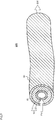
- FIG. 1 is a diagram schematically showing a configuration of an electromagnetic wave transmission cable 100 according to the present embodiment.
- the electromagnetic wave transmission cable 100 includes a hollow waveguide tube 10 including a hollow dielectric layer in which a waveguide of tubular shape is formed, and a foamed resin member 20 covering the outside surface of the hollow waveguide tube 10.
- the dielectric layer and the hollow portion of the hollow waveguide tube 10 form a waveguide for transmitting electromagnetic waves EW.
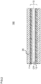
- FIG. 2 is a longitudinal cross-sectional view of the electromagnetic wave transmission cable 100.
- the hollow waveguide tube 10 includes a dielectric layer 11 and a hollow region 12.
- the dielectric layer 11 is formed in a tubular shape to surround the hollow region 12 with a center axis CA at the center.
- the dielectric layer 11 has a rotationally symmetrical shape about the center axis CA.
- FIG. 1 shows a case where the cross section of the dielectric layer 11 in a direction perpendicular to the center axis CA has a circular outer rim, whereas the outer rim may have an oblong circular shape, an elliptical shape, a rectangular shape, etc.
- the dielectric layer 11 is made of a fluorocarbon resin PTFE (polytetrafluoroethylene), for example.
- the dielectric layer 11 thus has a refractive index of approximately 1.5.
- the hollow region 12 is formed in a rotationally symmetrical shape about the center axis CA along the inner diameter of the hollow waveguide tube 10 (i.e., the inner diameter of the dielectric tube made of the dielectric layer 11).
- the dielectric waveguide does not necessarily need to have a rotationally symmetrical shape as long as desired performance is obtained.
- FIG. 1 shows a case where the cross section of the hollow region 12 (i.e., the cross section of the waveguide) in a direction perpendicular to the center axis CA is circular, the cross section may have an oblong circular shape, an elliptical shape, a rectangular shape, etc.
- the inner diameter of the hollow waveguide tube 10 is desirably set to be smaller than the wavelength.
- the inner diameter of the hollow waveguide tube 10 is desirably set to be greater than the half-wavelength since the electromagnetic wave confinement effect weakens as the hollow region 12 decreases.
- the inner diameter of the hollow waveguide tube 10 according to the present embodiment is therefore set to be equal to or greater than the half-wavelength and not greater than the wavelength.
- the outer diameter of the hollow waveguide tube 10 is desirably greater than a wavelength equivalent (wavelength ⁇ refractive index).
- the outer diameter of the hollow waveguide tube is desirably not so large. Specifically, the outer diameter is desirably less than or equal to twice the wavelength equivalent.
- the outer diameter of the hollow waveguide tube 10 according to the present embodiment is therefore set to be equal to or greater than the wavelength equivalent and not greater than twice the wavelength equivalent.
- the thickness of the dielectric layer 11 of the hollow waveguide tube 10 is desirably set to be smaller than the wavelength.
- the thickness of the dielectric layer 11 is desirably set to be greater than 1/10 the wavelength.
- the thickness of the dielectric layer 11 according to the present embodiment is therefore set to be equivalent to or greater than 1/10 the wavelength and not greater than the wavelength.
- the foamed resin member 20 extends in the longitudinal direction of the hollow waveguide tube 10 (i.e., waveguide direction) and covers the outside surface of the dielectric layer 11 (i.e., surface opposite from the hollow region 12) to surround the outer periphery of the hollow waveguide tube 10 with the center axis CA of the hollow waveguide tube 10 at the center.
- the foamed resin member 20 in its simplest form has a rotationally symmetrical cross-sectional shape about the center axis CA of the hollow waveguide tube 10.
- the foamed resin member 20 may have any shape as long as desired performance is obtained. For example, while FIG.
- the outer rim of the cross section of the foamed resin member 20 in the direction perpendicular to the center axis CA has a circular outer rim
- the outer rim may be an oblong circle, an ellipse, a rectangular, etc.
- the outer rim of the cross section of the foamed resin member 20 may have the same shape as or a different shape from that of the outer rim of the cross section of the dielectric layer 11.
- the foamed resin member 20 is made of foamed polystyrene.
- Foamed polystyrene has a fine intricate structure of polystyrene having a refractive index of 1.6 and air having a refractive index of 1, and includes a lot of fine reflection interfaces between polystyrene that is the dielectric and air.
- low-expansion-ratio foamed polystyrene used as a packaging material was measured in a bulk state and found to have an average refractive index (refractive index on the assumption that the bulk material was a uniform medium of a single substance) of approximately 1.1 at 0.1 to 0.5 THz. This result demonstrates that a large amount of air is mixed in foamed polystyrene.
- the foamed resin member 20 contains a large amount of air, and the ratio of polystyrene which is in contact with the surface of the hollow waveguide tube 10 is extremely low. This can significantly reduce the leakage of electromagnetic waves even in situations where a metal, a human body, or the like comes into contact with the outside surface of the foamed resin member 20 (i.e., surface opposite from the surface which is in contact with the hollow waveguide tube 10).
- Too small a thickness of the foamed resin member 20 lowers the electromagnetic wave confinement effect.
- a sufficient effect was not obtained if the thickness of the foamed resin member 20 was less than 1 mm.
- the thickness of the foamed resin member 20 is therefore desirably greater than or equal to a thickness equivalent to the wavelength of the electromagnetic waves to be transmitted (wavelength ⁇ average refractive index). Since too great a thickness results in poor handleability, the thickness of the foamed resin member 20 is desirably set to 50 mm or less, preferably 10 mm or less.
- the surface of the hollow waveguide tube 10 is covered with the foamed resin member 20.
- the foamed resin member 20 contains a large amount of air and has an average refractive index lower than the refractive index of the dielectric layer 11 of the hollow waveguide tube 10.
- the electromagnetic wave confinement effect of the hollow waveguide tube 10 can be maintained even in situations where a metal, human body, or other object comes into contact therewith.
- the foamed resin member 20 is described to be made of foamed polystyrene.
- the material of the foamed resin member 20 is not limited thereto, and the foamed resin member 20 may be made of foamed polyurethane, foamed polyolefin, foamed polyolefin (foamed polyethylene, foamed polypropylene), foamed polytetrafluoroethylene (PTFE), or the like.
- the outer diameter of the hollow waveguide tube 10 is smaller than the wavelength equivalent (wavelength ⁇ refractive index), there occurs a component propagating over the outer periphery of the waveguide tube. This can cause an adverse effect if the covering foamed resin has an attenuation factor higher than that of air. If the material of the foamed resin member 20 is polystyrene (PS), polyethylene (PE), or fluorocarbon resin (PTFE), the foamed material has an average attenuation factor of 0.1 cm -1 or less, and the problem does not matter much.
- PS polystyrene
- PE polyethylene
- PTFE fluorocarbon resin
- the foamed resin member 20 is described to be made of foamed polystyrene and have an average refractive index of approximately 1.1 at 0.1 to 0.5 THz, for example.
- the average refractive index of the foamed resin member 20 is not limited thereto. Since the electromagnetic wave confinement effect results from a low refractive index, the foamed resin member 20 desirably has a high expansion ratio. However, too high an expansion ratio increases softness and results in poor handleability.
- the foamed resin member 20 is therefore desirably foamed to an extent such that the average refractive index in the transmission frequency band in a bulk state falls below 1.4.
- the dielectric layer 11 of the hollow waveguide tube 10 and the foamed resin member 20 may be made of the same type of material by using a foam of foamed fluorocarbon resin (polytetrafluoroethylene) (PTFE) as the material of the foamed resin member 20.
- PTFE polytetrafluoroethylene
- the hollow waveguide tube 10 and the foamed resin member 20 can be constituted by changing the expansion ratio of the same material.
- a three-dimensional structure may be formed on the surface of the foamed resin member 20.
- the electromagnetic wave transmission cable 100 can be made flexible by forming a protruding structure on the outside surface opposite from the inside surface that is in contact with the dielectric layer 11 as shown in FIG. 3(a) .
- the electromagnetic wave confinement effect can be enhanced by forming a protruding structure on the inside surface that is in contact with the dielectric layer as shown in FIG. 3(b) .
- the three-dimensional structure formed on the surface(s) of the foamed resin member 20 may have a notch shape or other pit-and-projection shape.
- an outer coating 30 covering the outside surface of the foamed resin member 20 may be provided along the longitudinal direction of the hollow waveguide tube 10 and the foamed resin member 20.
- the foamed resin member 20 instead of covering the entire hollow waveguide tube 10 with the foamed resin member 20, only parts that can come into contact with other members, such as connector units for connecting waveguide tubes to each other and supports for holding the waveguide tube(s) at a predetermined height, may be configured to be covered with the foamed resin member 20.
- the foamed resin member 20 may be formed over a predetermined length (distance) in the longitudinal direction of the hollow waveguide tube, and may be provided at a plurality of positions.
- the expansion ratio of the foamed resin member 20 may be changed stepwise between regions closer to a contact surface that is in contact with the dielectric layer 11 (i.e., inside) and regions farther from the contact surface (i.e., outside). For example, in the inside regions closer to the contact surface with the dielectric layer 11, the expansion ratio can be increased to reduce the refractive index and enhance the electromagnetic wave confinement effect. In the outside regions farther from the contact surface with the dielectric layer 11, the expansion ratio can be reduced to increase cable rigidity.
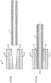
- a foamed resin member 20 can be used as a connector 40 in a connector unit for connecting waveguide tubes to each other.
- foamed resin members 20 are provided on the inner sides of a pair of holding members 41A and 41B to form a tapered gap.
- the hollow waveguide tube 10 can thus be inserted into the connector 40 so that the hollow waveguide tube is supported. This enables easy and reliable cable positioning while preventing the electromagnetic wave confinement effect from being hampered by contact with the holding members 41A and 41B.
- the dielectric layer 11 may be made of e-PTFE (expanded polytetrafluoroethylene) which is PTFE given stretch processing.
- e-PTFE expanded polytetrafluoroethylene
- e-PTFE can be obtained, for example, by stretching a PTFE material at least in one direction to provide continuous porosity (structure including a large number of continuous pores) and then sintering-fixing (fixing by sintering) the resultant at high temperature.
- the stretched porous resin (e-PTFE) used in the present embodiment has characteristic fine nodes and fine fiber structures in the stretching direction, and can thus function as a medium having a low average refractive index without increasing the electromagnetic wave transmission loss.
- the porosity of the stretched porous resin (the proportion of porous portions in the resin) can be selected from among 30% to 90% depending on the intended use.
- a refractive index difference of at least 0.01 or so is need.
- the desirable porosity derived therefrom is 70% or less.
- the optimum range of the porosity of the stretched porous resin of the dielectric layer 11 according to the present embodiment is therefore 30% to 70%.
- FIG. 7 is a diagram schematically showing a configuration of an electromagnetic wave transmission cable 200 according to the present embodiment.
- the electromagnetic wave transmission cable 200 includes a hollow waveguide tube 10 including a hollow dielectric layer in which a waveguide of tubular shape, a foamed resin member 20 covering the outside surface of the hollow waveguide tube 10, and a metal film 50 covering the outside surface of the foamed resin member 20.
- FIG. 8 is a longitudinal cross-sectional view of the electromagnetic wave transmission cable 200.
- the hollow waveguide tube 10 includes a dielectric layer 11 and a hollow region 12.
- the dielectric layer 11 is made of a resin material having a low refractive index or a low complex refractive index, such as PTFE (polytetrafluoroethylene), e-PTFE (expanded polytetrafluoroethylene) formed by stretching PTFE to provide continuous porosity and fixing the same by sintering, and PE (polyethylene).
- PTFE polytetrafluoroethylene
- e-PTFE expanded polytetrafluoroethylene formed by stretching PTFE to provide continuous porosity and fixing the same by sintering
- PE polyethylene
- the tube i.e. dielectric layer 11
- the tube desirably has a small thickness.
- the foamed resin member 20 is arranged to surround the outer periphery of the hollow waveguide tube 10.
- the foamed resin member 20 needs to have a refractive index lower than that of the dielectric constituting the dielectric layer 11 of the hollow waveguide tube 10. The closer to 1 the refractive index is, the better.
- the foamed resin member 20 is formed on the outer peripheral surface of the hollow waveguide tube 10, for example, by a method of inserting the hollow waveguide tube 10 into the inside of a foamed resin of hollow shape, a method of winding foamed resin around the hollow waveguide tube 10, or other methods.
- the metal film 50 has a rotationally symmetrical shape about the center axis CA.
- the metal film 50 extends in the longitudinal direction of the hollow waveguide tube 10 and the foamed resin member 20, and further covers the outside surface of the foamed resin member 20 covering the hollow waveguide tube 10 to surround the outer periphery of the foamed resin member 20 with the center axis CA at the center.
- the metal film 50 may have any shape as long as desired performance is obtained. While FIG.
- the outer rim of the cross section of the metal film 50 may have the same shape as or a different shape from that of the cross section of the hollow waveguide tube 10 or the foamed resin member 20.
- the metal film 50 may have any shape covering the foamed resin member 20.
- the metal film 50 is made of a metal having a relatively high conductivity, such as gold, silver, and copper.
- the metal film 50 may have a thickness of about 1 ⁇ m or more.
- the metal film 50 is formed, for example, by a method of directly forming a metal film on the surface of the foamed resin member 20, a method of forming a metal film on the surface of a dielectric sheet to fabricate a metal-coated sheet in advance and then winding the metal-coated sheet on the foamed resin member 20 with the metal surface toward the foamed resin member 20, or other methods.
- the outer peripheral portion of the metal film 50 is covered with a protective film (not shown) made of a dielectric or the like.
- the protective film has only a protective function and does not contribute to electromagnetic wave transmission.
- the metal film 50 is formed by the method of winding a metal-coated sheet on the foamed resin member 20, the dielectric sheet can be left unremoved and used as a protective film.
- the metal film 50 is formed to further cover the outside surface of the foamed resin member 20 covering the hollow waveguide tube 10. The effect of the metal film 50 will be described with reference to FIGs. 9 and 10 .
- FIG. 9 is a graph showing a relationship between the thickness of the dielectric layer 11 (dielectric tube) made of e-PTFE and the transmission loss, depending on the presence or absence of the outer covering.
- the transfer loss decreases as the thickness of the dielectric layer decreases (dielectric tube becomes thinner).
- the transmission loss is lower than without an outer covering, and the transmission loss decreases with the decreasing thickness of the dielectric layer within a range where the dielectric layer (dielectric tube) has a certain thickness or more (in FIG. 10 , approximately 0.2 mm to 0.7 mm). However, if the thickness of the dielectric layer falls below a certain value (0.2 mm), the transmission loss degrades to a nontransmissible degree (in FIG. 9 , shown as immeasurable).
- the transmission loss decreases in proportion to the thickness of the dielectric layer.
- the transmission loss does not degrade even in the range where the thickness of the dielectric layer is less than the certain value (0.2 mm).
- FIG. 10 is a graph showing a relationship between the thickness of the dielectric layer and an effective refractive index, depending on the presence or absence of the outer covering.
- the effective refractive index is a parameter that represents an average refractive index of the medium contributing to the electromagnetic wave transmission and characterizes the transmission state of the electromagnetic waves.
- the effective refractive index asymptotically approaches the refractive index of the foamed resin (1.016) (in the case of foamed polystyrene having an expansion ratio of approximately 30 times) as the thickness of the dielectric layer decreases (dielectric tube becomes thinner).
- the transmission with the foamed resin as the propagation medium is unstable in terms of the confinement of the electromagnetic waves, and eventually becomes incapable of transmission.
- the effective refractive index does not asymptotically approach the refractive index of the foamed resin, but the effective refractive index decreases with the decreasing thickness of the dielectric layer. This indicates that the propagation medium of the electromagnetic waves does not shift to the foamed resin and the electromagnetic waves are stably transmitted with the dielectric layer (dielectric tube) as the waveguide.
- the outer covering of the hollow waveguide tube 10 has a double structure including the foamed resin member 20 and the metal film 50. This can suppress a drop in the transmission loss occurring if the covering is the foamed resin alone. More specifically, if the dielectric layer of the hollow waveguide tube is covered with only the foamed resin, electromagnetic wave transmission can no longer be transmitted once the transmission loss falls below a lower limit value determined by the physical property values of the dielectric waveguide and the foamed resin (for example, the effective refractive index falls below the refractive index of the foamed resin).
- the metal film 50 functions as a shield against external electromagnetic waves (noise). Since the hollow waveguide tube 10 is shielded from outside, electromagnetic waves can be stably transmitted.
- the thickness of the entire covering portion can be reduced for miniaturization, compared to when the hollow waveguide tube is covered with only a foamed resin.
- the metal film 50 does not necessarily need to cover the entire outside surface of the foamed resin member 20.
- the metal film 50 may be patterned to partly cover the outside surface of the foamed resin member 20 at intervals less than or equal to the wavelength of the electromagnetic waves EW.
- the patterning of the metal film may be implemented, for example, by a method of winding a metal thin wire or a method of putting a net such as a braided shield.
- the patterning of the metal film may be implemented by forming a wire grid or a metamaterial structure by using a mask during film formation.
- the needed thickness of the foamed resin member 20 can be reduced by adjusting the structures and materials of the dielectric waveguide 10 and the metal film 50.
- the metal film 50 is described to be made of a metal such as gold, silver, and copper, the metal film 50 may be made of aluminum or an alloy.
- the metal constituting the metal film 50 desirably has a high conductivity, whereas any metal having some conductivity can be used since even a metal having a low conductivity has the effect of improving the transmission characteristic.
- a dielectric film may be used as the outer coating that covers the foamed resin member 20.
- a dielectric film having a refractive index of about 1.4 or more can provide a sufficient refractive index difference at the interface.
- the electromagnetic wave transmission cable according to the present embodiment can be used, for example, as a cable for in-vehicle high capacity high speed information communication to replace a vehicle information harness of an automobile and the like, or as a cable intended for a data center, moving image transmission, and the like where high capacity communication is needed.
Landscapes
- Physics & Mathematics (AREA)
- General Physics & Mathematics (AREA)
- Optics & Photonics (AREA)
- Engineering & Computer Science (AREA)
- Microelectronics & Electronic Packaging (AREA)
- Chemical & Material Sciences (AREA)
- Crystallography & Structural Chemistry (AREA)
- Waveguides (AREA)
Abstract
Description
- The present invention relates to an electromagnetic wave transmission cable.
- A hollow waveguide tube made of a dielectric such as a resin has a light weight, high flexibility, a low transmission loss, and high transmission efficiency compared to metal cables such as a coaxial cable and metal waveguide tubes, and is thus effective as a cable for mainly transmitting millimeter waves (30 to 300 GHz) to THz-band (0.1 to 100 THz) electromagnetic waves.
- While a hollow waveguide tube made of a single-layer dielectric tube has a confinement effect with respect to the surrounding air, the confinement effect can be hampered and electromagnetic waves leak and scatter off if a metal or another dielectric, such as a human body in particular, comes into contact with the outer wall of the waveguide tube.
- A transmission path that confines and transmits electromagnetic waves by stacking two types of dielectrics in layers to construct a Bragg mirror on the outer periphery of a waveguide tube has thus been conceived (for example, Patent Literature 1).
- Patent Literature 1: United States Patent Application Publication No.
2009/0097809 - According to the foregoing conventional technique, different materials need to be stacked in layers to constitute the Bragg mirror. There have thus been problems of increased man-hours and high manufacturing cost. In addition, the thicknesses of the respective layers need to be designed on the basis of the wavelength of transmission, and there has been a problem of wavelength dependence.
- Among examples of problems to be solved by the present invention is that the electromagnetic wave confinement effect is hampered when another object is in contact with the hollow waveguide tube.
- The invention according to
claim 1 is an electromagnetic wave transmission cable for transmitting an electromagnetic wave, comprising: a hollow waveguide tube including a hollow dielectric layer formed in a tubular shape; and a foamed resin member that is provided over a predetermined length in a longitudinal direction of the hollow waveguide tube and covers a surface of the dielectric layer to surround an outer periphery of the hollow waveguide tube. -
-
FIG. 1 is a diagram schematically showing an electromagnetic wave transmission cable according to the present invention. -
FIG. 2 is a longitudinal cross-sectional view of the electromagnetic wave transmission cable according to the present invention. -
FIG. 3 is a longitudinal cross-sectional view showing modifications of the electromagnetic wave transmission cable according to the present invention. -
FIG. 4 is a diagram schematically showing a modification of the electromagnetic wave transmission cable according to the present invention. -
FIG. 5 is a longitudinal cross-sectional view showing a modification of the electromagnetic wave transmission cable according to the present invention. -
FIG. 6 is a longitudinal cross-sectional view showing a modification of the electromagnetic wave transmission cable according to the present invention. -
FIG. 7 is a diagram schematically showing an electromagnetic wave transmission cable according to a second embodiment. -
FIG. 8 is a longitudinal cross-sectional view of the electromagnetic wave transmission cable according to the second embodiment. -
FIG. 9 is a chart showing an example of a relationship between the presence or absence of an outer covering and a transmission loss. -
FIG. 10 is a chart showing a relationship between the presence or absence of the outer covering and an effective refractive index. - Embodiments of the present invention will be described below with reference to the drawings. In the following description and the accompanying drawings, substantially the same or equivalent parts are designated by the same reference numerals.
-
FIG. 1 is a diagram schematically showing a configuration of an electromagneticwave transmission cable 100 according to the present embodiment. The electromagneticwave transmission cable 100 includes ahollow waveguide tube 10 including a hollow dielectric layer in which a waveguide of tubular shape is formed, and afoamed resin member 20 covering the outside surface of thehollow waveguide tube 10. The dielectric layer and the hollow portion of thehollow waveguide tube 10 form a waveguide for transmitting electromagnetic waves EW. -
FIG. 2 is a longitudinal cross-sectional view of the electromagneticwave transmission cable 100. Thehollow waveguide tube 10 includes adielectric layer 11 and ahollow region 12. - The
dielectric layer 11 is formed in a tubular shape to surround thehollow region 12 with a center axis CA at the center. In other words, thedielectric layer 11 has a rotationally symmetrical shape about the center axis CA. For example,FIG. 1 shows a case where the cross section of thedielectric layer 11 in a direction perpendicular to the center axis CA has a circular outer rim, whereas the outer rim may have an oblong circular shape, an elliptical shape, a rectangular shape, etc. Thedielectric layer 11 is made of a fluorocarbon resin PTFE (polytetrafluoroethylene), for example. Thedielectric layer 11 thus has a refractive index of approximately 1.5. - The
hollow region 12 is formed in a rotationally symmetrical shape about the center axis CA along the inner diameter of the hollow waveguide tube 10 (i.e., the inner diameter of the dielectric tube made of the dielectric layer 11). Note that the dielectric waveguide does not necessarily need to have a rotationally symmetrical shape as long as desired performance is obtained. For example, whileFIG. 1 shows a case where the cross section of the hollow region 12 (i.e., the cross section of the waveguide) in a direction perpendicular to the center axis CA is circular, the cross section may have an oblong circular shape, an elliptical shape, a rectangular shape, etc. - There is a close relationship between the wavelength of the electromagnetic waves EW flowing through the
hollow waveguide tube 10 and an optimum tube shape. For example, to enhance adherence to the HE11 mode of low transmission loss, the inner diameter of thehollow waveguide tube 10 is desirably set to be smaller than the wavelength. On the other hand, the inner diameter of thehollow waveguide tube 10 is desirably set to be greater than the half-wavelength since the electromagnetic wave confinement effect weakens as thehollow region 12 decreases. The inner diameter of thehollow waveguide tube 10 according to the present embodiment is therefore set to be equal to or greater than the half-wavelength and not greater than the wavelength. - The outer diameter of the
hollow waveguide tube 10 is desirably greater than a wavelength equivalent (wavelength × refractive index). On the other hand, to make the transmission in the HE11 mode dominant, the outer diameter of the hollow waveguide tube is desirably not so large. Specifically, the outer diameter is desirably less than or equal to twice the wavelength equivalent. The outer diameter of thehollow waveguide tube 10 according to the present embodiment is therefore set to be equal to or greater than the wavelength equivalent and not greater than twice the wavelength equivalent. - To enhance the adherence to the HE11 mode of low transmission loss, the thickness of the
dielectric layer 11 of thehollow waveguide tube 10 is desirably set to be smaller than the wavelength. However, since too thin adielectric layer 11 fails to provide strength needed for the waveguide, the thickness of thedielectric layer 11 is desirably set to be greater than 1/10 the wavelength. The thickness of thedielectric layer 11 according to the present embodiment is therefore set to be equivalent to or greater than 1/10 the wavelength and not greater than the wavelength. - The
foamed resin member 20 extends in the longitudinal direction of the hollow waveguide tube 10 (i.e., waveguide direction) and covers the outside surface of the dielectric layer 11 (i.e., surface opposite from the hollow region 12) to surround the outer periphery of thehollow waveguide tube 10 with the center axis CA of thehollow waveguide tube 10 at the center. Thefoamed resin member 20 in its simplest form has a rotationally symmetrical cross-sectional shape about the center axis CA of thehollow waveguide tube 10. However, thefoamed resin member 20 may have any shape as long as desired performance is obtained. For example, whileFIG. 1 shows a case where the cross section of thefoamed resin member 20 in the direction perpendicular to the center axis CA has a circular outer rim, the outer rim may be an oblong circle, an ellipse, a rectangular, etc. The outer rim of the cross section of thefoamed resin member 20 may have the same shape as or a different shape from that of the outer rim of the cross section of thedielectric layer 11. - For example, the
foamed resin member 20 is made of foamed polystyrene. Foamed polystyrene has a fine intricate structure of polystyrene having a refractive index of 1.6 and air having a refractive index of 1, and includes a lot of fine reflection interfaces between polystyrene that is the dielectric and air. For example, low-expansion-ratio foamed polystyrene used as a packaging material was measured in a bulk state and found to have an average refractive index (refractive index on the assumption that the bulk material was a uniform medium of a single substance) of approximately 1.1 at 0.1 to 0.5 THz. This result demonstrates that a large amount of air is mixed in foamed polystyrene. - As described above, the
foamed resin member 20 contains a large amount of air, and the ratio of polystyrene which is in contact with the surface of thehollow waveguide tube 10 is extremely low. This can significantly reduce the leakage of electromagnetic waves even in situations where a metal, a human body, or the like comes into contact with the outside surface of the foamed resin member 20 (i.e., surface opposite from the surface which is in contact with the hollow waveguide tube 10). - Too small a thickness of the foamed
resin member 20 lowers the electromagnetic wave confinement effect. For example, in an experiment performed by using a PTFE hollow waveguide tube having a waveguide frequency of 300 GHz, an outer diameter of 0.9 mm, and an inner diameter of 0.5 mm, a sufficient effect was not obtained if the thickness of the foamedresin member 20 was less than 1 mm. The thickness of the foamed resin member 20 (thickness of the covering portion) is therefore desirably greater than or equal to a thickness equivalent to the wavelength of the electromagnetic waves to be transmitted (wavelength × average refractive index). Since too great a thickness results in poor handleability, the thickness of the foamedresin member 20 is desirably set to 50 mm or less, preferably 10 mm or less. - As described above, in the electromagnetic
wave transmission cable 100 according to the present embodiment, the surface of thehollow waveguide tube 10 is covered with the foamedresin member 20. The foamedresin member 20 contains a large amount of air and has an average refractive index lower than the refractive index of thedielectric layer 11 of thehollow waveguide tube 10. - With such a configuration, the electromagnetic wave confinement effect of the
hollow waveguide tube 10 can be maintained even in situations where a metal, human body, or other object comes into contact therewith. - The embodiment of the present invention is not limited to the foregoing one. For example, in the foregoing embodiment, the foamed
resin member 20 is described to be made of foamed polystyrene. However, the material of the foamedresin member 20 is not limited thereto, and the foamedresin member 20 may be made of foamed polyurethane, foamed polyolefin, foamed polyolefin (foamed polyethylene, foamed polypropylene), foamed polytetrafluoroethylene (PTFE), or the like. - If the outer diameter of the
hollow waveguide tube 10 is smaller than the wavelength equivalent (wavelength × refractive index), there occurs a component propagating over the outer periphery of the waveguide tube. This can cause an adverse effect if the covering foamed resin has an attenuation factor higher than that of air. If the material of the foamedresin member 20 is polystyrene (PS), polyethylene (PE), or fluorocarbon resin (PTFE), the foamed material has an average attenuation factor of 0.1 cm-1 or less, and the problem does not matter much. - In the foregoing embodiment, the foamed
resin member 20 is described to be made of foamed polystyrene and have an average refractive index of approximately 1.1 at 0.1 to 0.5 THz, for example. However, the average refractive index of the foamedresin member 20 is not limited thereto. Since the electromagnetic wave confinement effect results from a low refractive index, the foamedresin member 20 desirably has a high expansion ratio. However, too high an expansion ratio increases softness and results in poor handleability. The foamedresin member 20 is therefore desirably foamed to an extent such that the average refractive index in the transmission frequency band in a bulk state falls below 1.4. - Unlike the foregoing embodiment, the
dielectric layer 11 of thehollow waveguide tube 10 and the foamedresin member 20 may be made of the same type of material by using a foam of foamed fluorocarbon resin (polytetrafluoroethylene) (PTFE) as the material of the foamedresin member 20. In other words, thehollow waveguide tube 10 and the foamedresin member 20 can be constituted by changing the expansion ratio of the same material. - A three-dimensional structure may be formed on the surface of the foamed
resin member 20. For example, the electromagneticwave transmission cable 100 can be made flexible by forming a protruding structure on the outside surface opposite from the inside surface that is in contact with thedielectric layer 11 as shown inFIG. 3(a) . The electromagnetic wave confinement effect can be enhanced by forming a protruding structure on the inside surface that is in contact with the dielectric layer as shown inFIG. 3(b) . The three-dimensional structure formed on the surface(s) of the foamedresin member 20 may have a notch shape or other pit-and-projection shape. - To protect the electromagnetic
wave transmission cable 100 from collapsing, as shown inFig. 3(c) , anouter coating 30 covering the outside surface of the foamedresin member 20 may be provided along the longitudinal direction of thehollow waveguide tube 10 and the foamedresin member 20. - As shown in
FIG. 4 , instead of covering the entirehollow waveguide tube 10 with the foamedresin member 20, only parts that can come into contact with other members, such as connector units for connecting waveguide tubes to each other and supports for holding the waveguide tube(s) at a predetermined height, may be configured to be covered with the foamedresin member 20. In other words, the foamedresin member 20 may be formed over a predetermined length (distance) in the longitudinal direction of the hollow waveguide tube, and may be provided at a plurality of positions. - As shown in
FIG. 5 , the expansion ratio of the foamedresin member 20 may be changed stepwise between regions closer to a contact surface that is in contact with the dielectric layer 11 (i.e., inside) and regions farther from the contact surface (i.e., outside). For example, in the inside regions closer to the contact surface with thedielectric layer 11, the expansion ratio can be increased to reduce the refractive index and enhance the electromagnetic wave confinement effect. In the outside regions farther from the contact surface with thedielectric layer 11, the expansion ratio can be reduced to increase cable rigidity. This can be implemented, for example, by dividing the regions closer to and farther from the contact surface of the foamedresin member 20 with thedielectric waveguide 10 into a plurality of areas, and reducing the expansion ratios of the respective areas stepwise from the areas closer to the contact surface to the farther areas. - As shown in
FIGs. 6(a) and 6(b) , a foamedresin member 20 can be used as aconnector 40 in a connector unit for connecting waveguide tubes to each other. For example, as shown inFIG. 6(a) , by utilizing the property of being deformable of the foamedresin member 20, foamedresin members 20 are provided on the inner sides of a pair of holdingmembers FIG. 6(b) , thehollow waveguide tube 10 can thus be inserted into theconnector 40 so that the hollow waveguide tube is supported. This enables easy and reliable cable positioning while preventing the electromagnetic wave confinement effect from being hampered by contact with the holdingmembers - In the electromagnetic
wave transmission cable 100 according to the present embodiment, thedielectric layer 11 may be made of e-PTFE (expanded polytetrafluoroethylene) which is PTFE given stretch processing. e-PTFE can be obtained, for example, by stretching a PTFE material at least in one direction to provide continuous porosity (structure including a large number of continuous pores) and then sintering-fixing (fixing by sintering) the resultant at high temperature. The stretched porous resin (e-PTFE) used in the present embodiment has characteristic fine nodes and fine fiber structures in the stretching direction, and can thus function as a medium having a low average refractive index without increasing the electromagnetic wave transmission loss. - The porosity of the stretched porous resin (the proportion of porous portions in the resin) can be selected from among 30% to 90% depending on the intended use. To cover the outside with the foamed
resin member 20 as in the present embodiment, there needs to be a refractive index difference from the foamedresin member 20. To suppress the electromagnetic wave transmission loss, a refractive index difference of at least 0.01 or so is need. The desirable porosity derived therefrom is 70% or less. The optimum range of the porosity of the stretched porous resin of thedielectric layer 11 according to the present embodiment is therefore 30% to 70%. -
FIG. 7 is a diagram schematically showing a configuration of an electromagneticwave transmission cable 200 according to the present embodiment. The electromagneticwave transmission cable 200 includes ahollow waveguide tube 10 including a hollow dielectric layer in which a waveguide of tubular shape, a foamedresin member 20 covering the outside surface of thehollow waveguide tube 10, and ametal film 50 covering the outside surface of the foamedresin member 20. -
FIG. 8 is a longitudinal cross-sectional view of the electromagneticwave transmission cable 200. Thehollow waveguide tube 10 includes adielectric layer 11 and ahollow region 12. - The
dielectric layer 11 is made of a resin material having a low refractive index or a low complex refractive index, such as PTFE (polytetrafluoroethylene), e-PTFE (expanded polytetrafluoroethylene) formed by stretching PTFE to provide continuous porosity and fixing the same by sintering, and PE (polyethylene). To reduce a transmission loss, the tube (i.e. dielectric layer 11) desirably has a small thickness. - The foamed
resin member 20 is arranged to surround the outer periphery of thehollow waveguide tube 10. The foamedresin member 20 needs to have a refractive index lower than that of the dielectric constituting thedielectric layer 11 of thehollow waveguide tube 10. The closer to 1 the refractive index is, the better. - The foamed
resin member 20 is formed on the outer peripheral surface of thehollow waveguide tube 10, for example, by a method of inserting thehollow waveguide tube 10 into the inside of a foamed resin of hollow shape, a method of winding foamed resin around thehollow waveguide tube 10, or other methods. - Like the
hollow waveguide tube 10 and the foamedresin member 20, themetal film 50 has a rotationally symmetrical shape about the center axis CA. Themetal film 50 extends in the longitudinal direction of thehollow waveguide tube 10 and the foamedresin member 20, and further covers the outside surface of the foamedresin member 20 covering thehollow waveguide tube 10 to surround the outer periphery of the foamedresin member 20 with the center axis CA at the center. Note that themetal film 50 may have any shape as long as desired performance is obtained. WhileFIG. 7 shows a case where the cross section of themetal film 50 in a direction perpendicular to the center axis CA has a circular outer rim, the outer rim may be an oblong circle, an ellipse, a rectangular, etc. The outer rim of the cross section of themetal film 50 may have the same shape as or a different shape from that of the cross section of thehollow waveguide tube 10 or the foamedresin member 20. In other words, themetal film 50 may have any shape covering the foamedresin member 20. - The
metal film 50 is made of a metal having a relatively high conductivity, such as gold, silver, and copper. Themetal film 50 may have a thickness of about 1 µm or more. Themetal film 50 is formed, for example, by a method of directly forming a metal film on the surface of the foamedresin member 20, a method of forming a metal film on the surface of a dielectric sheet to fabricate a metal-coated sheet in advance and then winding the metal-coated sheet on the foamedresin member 20 with the metal surface toward the foamedresin member 20, or other methods. - The outer peripheral portion of the
metal film 50 is covered with a protective film (not shown) made of a dielectric or the like. The protective film has only a protective function and does not contribute to electromagnetic wave transmission. For example, if themetal film 50 is formed by the method of winding a metal-coated sheet on the foamedresin member 20, the dielectric sheet can be left unremoved and used as a protective film. - As described above, in the electromagnetic
wave transmission cable 200 according to the present embodiment, themetal film 50 is formed to further cover the outside surface of the foamedresin member 20 covering thehollow waveguide tube 10. The effect of themetal film 50 will be described with reference toFIGs. 9 and10 . -
FIG. 9 is a graph showing a relationship between the thickness of the dielectric layer 11 (dielectric tube) made of e-PTFE and the transmission loss, depending on the presence or absence of the outer covering. - If the hollow waveguide tube is formed alone without any outer covering, as shown by a broken line in
FIG. 9 , the transfer loss decreases as the thickness of the dielectric layer decreases (dielectric tube becomes thinner). - If the outside surface of the dielectric layer of the hollow waveguide tube is covered with a foamed polystyrene resin having an expansion ratio of approximately 30 times, as shown by a dot-dashed line in
FIG. 9 , the transmission loss is lower than without an outer covering, and the transmission loss decreases with the decreasing thickness of the dielectric layer within a range where the dielectric layer (dielectric tube) has a certain thickness or more (inFIG. 10 , approximately 0.2 mm to 0.7 mm). However, if the thickness of the dielectric layer falls below a certain value (0.2 mm), the transmission loss degrades to a nontransmissible degree (inFIG. 9 , shown as immeasurable). - In contrast, if the outside surface of the foamed resin covering the hollow waveguide tube is further covered with a metal film, as shown by a solid line in
FIG. 9 , the transmission loss decreases in proportion to the thickness of the dielectric layer. The transmission loss does not degrade even in the range where the thickness of the dielectric layer is less than the certain value (0.2 mm). -
FIG. 10 is a graph showing a relationship between the thickness of the dielectric layer and an effective refractive index, depending on the presence or absence of the outer covering. The effective refractive index is a parameter that represents an average refractive index of the medium contributing to the electromagnetic wave transmission and characterizes the transmission state of the electromagnetic waves. - If the outside surface of the dielectric layer of the hollow waveguide tube is covered with a foamed resin, as shown by a dot-dashed line in
FIG. 10 , the effective refractive index asymptotically approaches the refractive index of the foamed resin (1.016) (in the case of foamed polystyrene having an expansion ratio of approximately 30 times) as the thickness of the dielectric layer decreases (dielectric tube becomes thinner). This indicates that the propagation medium of the electromagnetic waves shifts from the dielectric to the foamed resin as the thickness of the dielectric layer decreases. The transmission with the foamed resin as the propagation medium is unstable in terms of the confinement of the electromagnetic waves, and eventually becomes incapable of transmission. - In contrast, if the outside surface of the foamed resin is covered with the metal film, as shown by a solid line in
FIG. 10 , the effective refractive index does not asymptotically approach the refractive index of the foamed resin, but the effective refractive index decreases with the decreasing thickness of the dielectric layer. This indicates that the propagation medium of the electromagnetic waves does not shift to the foamed resin and the electromagnetic waves are stably transmitted with the dielectric layer (dielectric tube) as the waveguide. - As described above, in the electromagnetic
wave transmission cable 200 according to the present embodiment, the outer covering of thehollow waveguide tube 10 has a double structure including the foamedresin member 20 and themetal film 50. This can suppress a drop in the transmission loss occurring if the covering is the foamed resin alone. More specifically, if the dielectric layer of the hollow waveguide tube is covered with only the foamed resin, electromagnetic wave transmission can no longer be transmitted once the transmission loss falls below a lower limit value determined by the physical property values of the dielectric waveguide and the foamed resin (for example, the effective refractive index falls below the refractive index of the foamed resin). However, if the foamed resin (foamed resin member 20) is further covered with the metal film as in the present embodiment, transmission losses below the lower limit value (lower limit value of the transmission loss in the case of covering with only the foamed resin) can be achieved. - In the electromagnetic
wave transmission cable 200 according to the present embodiment, themetal film 50 functions as a shield against external electromagnetic waves (noise). Since thehollow waveguide tube 10 is shielded from outside, electromagnetic waves can be stably transmitted. - The thickness of the entire covering portion can be reduced for miniaturization, compared to when the hollow waveguide tube is covered with only a foamed resin.
- The
metal film 50 does not necessarily need to cover the entire outside surface of the foamedresin member 20. For example, themetal film 50 may be patterned to partly cover the outside surface of the foamedresin member 20 at intervals less than or equal to the wavelength of the electromagnetic waves EW. The patterning of the metal film may be implemented, for example, by a method of winding a metal thin wire or a method of putting a net such as a braided shield. The patterning of the metal film may be implemented by forming a wire grid or a metamaterial structure by using a mask during film formation. - The needed thickness of the foamed
resin member 20 can be reduced by adjusting the structures and materials of thedielectric waveguide 10 and themetal film 50. - While the
metal film 50 is described to be made of a metal such as gold, silver, and copper, themetal film 50 may be made of aluminum or an alloy. The metal constituting themetal film 50 desirably has a high conductivity, whereas any metal having some conductivity can be used since even a metal having a low conductivity has the effect of improving the transmission characteristic. - Instead of the
metal film 50, a dielectric film may be used as the outer coating that covers the foamedresin member 20. For example, a dielectric film having a refractive index of about 1.4 or more can provide a sufficient refractive index difference at the interface. - The electromagnetic wave transmission cable according to the present embodiment can be used, for example, as a cable for in-vehicle high capacity high speed information communication to replace a vehicle information harness of an automobile and the like, or as a cable intended for a data center, moving image transmission, and the like where high capacity communication is needed.
Claims (20)
- An electromagnetic wave transmission cable for transmitting an electromagnetic wave, comprising:a hollow waveguide tube including a hollow dielectric layer formed in a tubular shape; anda foamed resin member that is provided over a predetermined length in a longitudinal direction of the hollow waveguide tube and covers a surface of the dielectric layer to surround an outer periphery of the hollow waveguide tube.
- The electromagnetic wave transmission cable according to claim 1, wherein the foamed resin member has a rotationally symmetrical sectional shape about a center axis of the hollow waveguide tube.
- The electromagnetic wave transmission cable according to claim 1 or 2, wherein the foamed resin member has different expansion ratios between a region close to a contact surface that is in contact with the dielectric layer and a region far from the contact surface.
- The electromagnetic wave transmission cable according to claim 3, wherein the foamed resin member has a high expansion ratio in the region close to the contact surface and a low expansion ratio in the region far from the contact surface.
- The electromagnetic wave transmission cable according to any one of claims 1 to 4, wherein the foamed resin member covers an outside surface of the dielectric layer at a plurality of positions in the longitudinal direction of the hollow waveguide tube.
- The electromagnetic wave transmission cable according to any one of claims 1 to 5, wherein the foamed resin member includes a protruding structure on an inner surface that is in contact with the dielectric layer.
- The electromagnetic wave transmission cable according to any one of claims 1 to 6, wherein the foamed resin member includes a protruding structure on an outside surface opposite from an inside surface that is in contact with the dielectric layer.
- The electromagnetic wave transmission cable according to any one of claims 1 to 7, further comprising an outer coating that covers an outside surface of the foamed resin member along the longitudinal direction of the hollow waveguide tube and the foamed resin member.
- The electromagnetic wave transmission cable according to claim 8, wherein the outer coating is a metal film.
- The electromagnetic wave transmission cable according to claim 8, wherein the outer coating is a dielectric.
- The electromagnetic wave transmission cable according to claim 9 or 10, further comprising a protective film that covers an outside surface of the outer coating along the longitudinal direction of the hollow waveguide tube.
- The electromagnetic wave transmission cable according to claim 11, wherein the protective film is made of a material containing a dielectric material.
- The electromagnetic wave transmission cable according to any one of claims 1 to 12, wherein the foamed resin member is made of any one of foamed polystyrene, foamed polyurethane, foamed polyolefin, and foamed polytetrafluoroethylene.
- The electromagnetic wave transmission cable according to any one of claims 1 to 12, wherein the foamed resin member is made of the same type of foamed resin material as that of the dielectric layer.
- The electromagnetic wave transmission cable according to any one of claims 1 to 14, wherein the electromagnetic wave has a frequency of 30 to 100000 GHz.
- The electromagnetic wave transmission cable according to any one of claims 1 to 15, wherein the foamed resin member has an average refractive index of 1 or more and not more than 1.4 in a transmission frequency band of the electromagnetic wave.
- The electromagnetic wave transmission cable according to any one of claims 1 to 16, wherein the foamed resin member covering the dielectric layer has a thickness greater than or equal to a length expressed by a wavelength of the electromagnetic wave multiplied by an average refractive index of the foamed resin member.
- The electromagnetic wave transmission cable according to any one of claims 1 to 17, wherein the foamed resin member has an average attenuation factor of 0.1 cm-1 or less with respect to the electromagnetic wave.
- The electromagnetic wave transmission cable according to any one of claims 1 to 18, wherein the hollow waveguide tube has an outer diameter greater than or equal to a length expressed by a wavelength of the electromagnetic wave multiplied by a refractive index of the dielectric layer.
- The electromagnetic wave transmission cable according to any one of claims 1 to 19, wherein the dielectric layer is made of a dielectric containing a material having stretch porosity.
Applications Claiming Priority (2)
| Application Number | Priority Date | Filing Date | Title |
|---|---|---|---|
| JP2016232105 | 2016-11-30 | ||
| PCT/JP2017/037700 WO2018100908A1 (en) | 2016-11-30 | 2017-10-18 | Electromagnetic wave transmission cable |
Publications (4)
| Publication Number | Publication Date |
|---|---|
| EP3534194A1 true EP3534194A1 (en) | 2019-09-04 |
| EP3534194A4 EP3534194A4 (en) | 2020-07-01 |
| EP3534194C0 EP3534194C0 (en) | 2025-01-22 |
| EP3534194B1 EP3534194B1 (en) | 2025-01-22 |
Family
ID=62241489
Family Applications (1)
| Application Number | Title | Priority Date | Filing Date |
|---|---|---|---|
| EP17875524.5A Active EP3534194B1 (en) | 2016-11-30 | 2017-10-18 | Electromagnetic wave transmission cable |
Country Status (4)
| Country | Link |
|---|---|
| US (1) | US11018403B2 (en) |
| EP (1) | EP3534194B1 (en) |
| JP (2) | JP6667666B2 (en) |
| WO (1) | WO2018100908A1 (en) |
Families Citing this family (9)
| Publication number | Priority date | Publication date | Assignee | Title |
|---|---|---|---|---|
| TWI845510B (en) * | 2018-05-25 | 2024-06-21 | 美商山姆科技公司 | Electrical cable and waveguide with dielectric foam |
| HUE060990T2 (en) * | 2019-01-22 | 2023-04-28 | Grieshaber Vega Kg | Waveguide with high conductivity for high temperatures and high frequencies for fill level meters |
| CN112751422B (en) * | 2019-10-30 | 2024-08-06 | 中国石油化工股份有限公司 | Conveying pipeline for pipeline power transmission |
| US12021289B2 (en) | 2020-06-25 | 2024-06-25 | Intel Corporation | Components for millimeter-wave communication |
| US12126068B2 (en) | 2020-06-25 | 2024-10-22 | Intel Corporation | Millimeter-wave dielectric waveguide bundle including first and second adjacent dielectric waveguides having different core and/or cladding materials |
| US12126067B2 (en) * | 2020-06-25 | 2024-10-22 | Intel Corporation | Millimeter-wave dielectric waveguide including an opening of varying cross-section enclosed within a first material and the first material surrounded by a second material |
| US11955684B2 (en) | 2020-06-25 | 2024-04-09 | Intel Corporation | Components for millimeter-wave communication |
| US12166261B2 (en) | 2020-06-25 | 2024-12-10 | Intel Corporation | Components for millimeter-wave communication |
| WO2025027950A1 (en) * | 2023-07-31 | 2025-02-06 | ポリプラ・エボニック株式会社 | Waveguide |
Family Cites Families (15)
| Publication number | Priority date | Publication date | Assignee | Title |
|---|---|---|---|---|
| DE1590675C3 (en) | 1965-10-01 | 1974-07-18 | Telefunken Patentverwertungsgesellschaft Mbh, 7900 Ulm | Waveguide |
| JPS51138369A (en) * | 1975-05-26 | 1976-11-29 | Dainichi Nippon Cables Ltd | Mode exciter device for dielectric waveguide system |
| CH613565A5 (en) * | 1977-02-11 | 1979-09-28 | Patelhold Patentverwertung | |
| JPS5616303A (en) * | 1979-07-18 | 1981-02-17 | Shigeo Nishida | Low-loss leakage transmission line |
| JP2633866B2 (en) | 1987-10-08 | 1997-07-23 | 日立電線株式会社 | Hollow optical waveguide |
| US5221308A (en) | 1988-09-21 | 1993-06-22 | 3M | Low loss infrared transmitting hollow core optical fiber method of manufacture |
| GB2288469B (en) | 1994-04-15 | 1997-10-22 | Hitachi Cable | Optical hollow waveguide, method for fabricating the same, and laser transmission apparatus using the same |
| US7409132B2 (en) * | 2006-07-27 | 2008-08-05 | National Taiwan University | Plastic waveguide for terahertz wave |
| US20090097809A1 (en) | 2007-06-26 | 2009-04-16 | Corporation De L'ecole Polytechnique De Montreal | Ferroelectric all-polymer hollow bragg fibers for terahertz guidance |
| CN202600172U (en) * | 2009-06-12 | 2012-12-12 | 夏普株式会社 | Optical component and liquid crystal display device having same |
| WO2014159450A1 (en) * | 2013-03-11 | 2014-10-02 | The Regents Of The University Of California | Hollow plastic waveguide for data center communications |
| US9997819B2 (en) * | 2015-06-09 | 2018-06-12 | At&T Intellectual Property I, L.P. | Transmission medium and method for facilitating propagation of electromagnetic waves via a core |
| JP6414632B2 (en) * | 2015-03-31 | 2018-10-31 | ダイキン工業株式会社 | Dielectric waveguide line |
| US9748626B2 (en) | 2015-05-14 | 2017-08-29 | At&T Intellectual Property I, L.P. | Plurality of cables having different cross-sectional shapes which are bundled together to form a transmission medium |
| US10249925B2 (en) * | 2016-09-30 | 2019-04-02 | Intel Corporation | Dielectric waveguide bundle including a supporting feature for connecting first and second server boards |
-
2017
- 2017-10-18 US US16/465,497 patent/US11018403B2/en active Active
- 2017-10-18 EP EP17875524.5A patent/EP3534194B1/en active Active
- 2017-10-18 JP JP2018553704A patent/JP6667666B2/en active Active
- 2017-10-18 WO PCT/JP2017/037700 patent/WO2018100908A1/en not_active Ceased
-
2020
- 2020-02-25 JP JP2020029594A patent/JP2020092451A/en not_active Withdrawn
Also Published As
| Publication number | Publication date |
|---|---|
| JPWO2018100908A1 (en) | 2019-10-17 |
| WO2018100908A1 (en) | 2018-06-07 |
| JP2020092451A (en) | 2020-06-11 |
| US11018403B2 (en) | 2021-05-25 |
| US20190296416A1 (en) | 2019-09-26 |
| EP3534194C0 (en) | 2025-01-22 |
| JP6667666B2 (en) | 2020-03-18 |
| EP3534194A4 (en) | 2020-07-01 |
| EP3534194B1 (en) | 2025-01-22 |
Similar Documents
| Publication | Publication Date | Title |
|---|---|---|
| EP3534194B1 (en) | Electromagnetic wave transmission cable | |
| US10749238B2 (en) | Dielectric waveguide comprising a dielectric core surrounded by a dielectric cladding having a plurality of ribs that support the core within a conductive shield | |
| US8575488B2 (en) | Differential signal transmission cable | |
| KR102208519B1 (en) | Low-loss dielectric waveguide for transmission of millimeter-wave signals and cable comprising same | |
| KR102544452B1 (en) | Manufacturing Process of Ribbon Bundled Millimeter Waveguides | |
| JP6815848B2 (en) | Electromagnetic wave transmission cable | |
| WO2019069712A1 (en) | Electromagnetic wave transmission cable | |
| US20180268965A1 (en) | Data cable for high speed data transmissions and method of manufacturing the data cable | |
| JP2017147548A (en) | Flexible waveguide, connector, and electromagnetic wave transmission system | |
| KR20190065239A (en) | Dielectric waveguide cable | |
| CN113316866B (en) | Dielectric waveguide cable | |
| JP2026067961A (en) | Communication cable | |
| CN114207936B (en) | Dielectric waveguide | |
| CN109859888A (en) | A kind of high speed parallel cable of digital communication | |
| JP2015188146A (en) | Waveguide and method of manufacturing the same | |
| JP2010040200A (en) | Transmission cable | |
| CN108091429B (en) | Differential signal cable | |
| US3492607A (en) | Electromagnetic waveguides | |
| JP6825240B2 (en) | Waveguide | |
| JP2005294209A (en) | Leaky coaxial cable | |
| JP7147536B2 (en) | radio wave transmission cable | |
| JPH01170101A (en) | Dielectric waveguide with plastic core | |
| CN114696053B (en) | Circular waveguide transmission line for millimeter waves and its manufacturing method | |
| WO2022131258A1 (en) | Communication cable and manufacturing method therefor | |
| JP2005204023A (en) | High frequency electromagnetic antenna |
Legal Events
| Date | Code | Title | Description |
|---|---|---|---|
| STAA | Information on the status of an ep patent application or granted ep patent |
Free format text: STATUS: THE INTERNATIONAL PUBLICATION HAS BEEN MADE |
|
| PUAI | Public reference made under article 153(3) epc to a published international application that has entered the european phase |
Free format text: ORIGINAL CODE: 0009012 |
|
| STAA | Information on the status of an ep patent application or granted ep patent |
Free format text: STATUS: REQUEST FOR EXAMINATION WAS MADE |
|
| 17P | Request for examination filed |
Effective date: 20190529 |
|
| AK | Designated contracting states |
Kind code of ref document: A1 Designated state(s): AL AT BE BG CH CY CZ DE DK EE ES FI FR GB GR HR HU IE IS IT LI LT LU LV MC MK MT NL NO PL PT RO RS SE SI SK SM TR |
|
| AX | Request for extension of the european patent |
Extension state: BA ME |
|
| DAV | Request for validation of the european patent (deleted) | ||
| DAX | Request for extension of the european patent (deleted) | ||
| A4 | Supplementary search report drawn up and despatched |
Effective date: 20200602 |
|
| RIC1 | Information provided on ipc code assigned before grant |
Ipc: H01P 3/16 20060101ALI20200527BHEP Ipc: G02B 6/032 20060101AFI20200527BHEP |
|
| STAA | Information on the status of an ep patent application or granted ep patent |
Free format text: STATUS: EXAMINATION IS IN PROGRESS |
|
| 17Q | First examination report despatched |
Effective date: 20210721 |
|
| GRAP | Despatch of communication of intention to grant a patent |
Free format text: ORIGINAL CODE: EPIDOSNIGR1 |
|
| STAA | Information on the status of an ep patent application or granted ep patent |
Free format text: STATUS: GRANT OF PATENT IS INTENDED |
|
| INTG | Intention to grant announced |
Effective date: 20240919 |
|
| GRAS | Grant fee paid |
Free format text: ORIGINAL CODE: EPIDOSNIGR3 |
|
| GRAA | (expected) grant |
Free format text: ORIGINAL CODE: 0009210 |
|
| STAA | Information on the status of an ep patent application or granted ep patent |
Free format text: STATUS: THE PATENT HAS BEEN GRANTED |
|
| AK | Designated contracting states |
Kind code of ref document: B1 Designated state(s): AL AT BE BG CH CY CZ DE DK EE ES FI FR GB GR HR HU IE IS IT LI LT LU LV MC MK MT NL NO PL PT RO RS SE SI SK SM TR |
|
| REG | Reference to a national code |
Ref country code: GB Ref legal event code: FG4D |
|
| REG | Reference to a national code |
Ref country code: CH Ref legal event code: EP |
|
| REG | Reference to a national code |
Ref country code: IE Ref legal event code: FG4D |
|
| REG | Reference to a national code |
Ref country code: DE Ref legal event code: R096 Ref document number: 602017087484 Country of ref document: DE |
|
| U01 | Request for unitary effect filed |
Effective date: 20250122 |
|
| U07 | Unitary effect registered |
Designated state(s): AT BE BG DE DK EE FI FR IT LT LU LV MT NL PT RO SE SI Effective date: 20250128 |
|
| U79 | Statement concerning licences of right filed [unitary effect] |
Effective date: 20250128 |
|
| REG | Reference to a national code |
Ref country code: GB Ref legal event code: 746 Effective date: 20250218 |
|
| PG25 | Lapsed in a contracting state [announced via postgrant information from national office to epo] |
Ref country code: RS Free format text: LAPSE BECAUSE OF FAILURE TO SUBMIT A TRANSLATION OF THE DESCRIPTION OR TO PAY THE FEE WITHIN THE PRESCRIBED TIME-LIMIT Effective date: 20250422 |
|
| PG25 | Lapsed in a contracting state [announced via postgrant information from national office to epo] |
Ref country code: PL Free format text: LAPSE BECAUSE OF FAILURE TO SUBMIT A TRANSLATION OF THE DESCRIPTION OR TO PAY THE FEE WITHIN THE PRESCRIBED TIME-LIMIT Effective date: 20250122 |
|
| PG25 | Lapsed in a contracting state [announced via postgrant information from national office to epo] |
Ref country code: ES Free format text: LAPSE BECAUSE OF FAILURE TO SUBMIT A TRANSLATION OF THE DESCRIPTION OR TO PAY THE FEE WITHIN THE PRESCRIBED TIME-LIMIT Effective date: 20250122 |
|
| PG25 | Lapsed in a contracting state [announced via postgrant information from national office to epo] |
Ref country code: IS Free format text: LAPSE BECAUSE OF FAILURE TO SUBMIT A TRANSLATION OF THE DESCRIPTION OR TO PAY THE FEE WITHIN THE PRESCRIBED TIME-LIMIT Effective date: 20250522 Ref country code: NO Free format text: LAPSE BECAUSE OF FAILURE TO SUBMIT A TRANSLATION OF THE DESCRIPTION OR TO PAY THE FEE WITHIN THE PRESCRIBED TIME-LIMIT Effective date: 20250422 |
|
| PG25 | Lapsed in a contracting state [announced via postgrant information from national office to epo] |
Ref country code: HR Free format text: LAPSE BECAUSE OF FAILURE TO SUBMIT A TRANSLATION OF THE DESCRIPTION OR TO PAY THE FEE WITHIN THE PRESCRIBED TIME-LIMIT Effective date: 20250122 |
|
| PG25 | Lapsed in a contracting state [announced via postgrant information from national office to epo] |
Ref country code: GR Free format text: LAPSE BECAUSE OF FAILURE TO SUBMIT A TRANSLATION OF THE DESCRIPTION OR TO PAY THE FEE WITHIN THE PRESCRIBED TIME-LIMIT Effective date: 20250423 |
|
| PG25 | Lapsed in a contracting state [announced via postgrant information from national office to epo] |
Ref country code: SM Free format text: LAPSE BECAUSE OF FAILURE TO SUBMIT A TRANSLATION OF THE DESCRIPTION OR TO PAY THE FEE WITHIN THE PRESCRIBED TIME-LIMIT Effective date: 20250122 |
|
| PG25 | Lapsed in a contracting state [announced via postgrant information from national office to epo] |
Ref country code: CZ Free format text: LAPSE BECAUSE OF FAILURE TO SUBMIT A TRANSLATION OF THE DESCRIPTION OR TO PAY THE FEE WITHIN THE PRESCRIBED TIME-LIMIT Effective date: 20250122 |
|
| PG25 | Lapsed in a contracting state [announced via postgrant information from national office to epo] |
Ref country code: SK Free format text: LAPSE BECAUSE OF FAILURE TO SUBMIT A TRANSLATION OF THE DESCRIPTION OR TO PAY THE FEE WITHIN THE PRESCRIBED TIME-LIMIT Effective date: 20250122 |
|
| PLBE | No opposition filed within time limit |
Free format text: ORIGINAL CODE: 0009261 |
|
| STAA | Information on the status of an ep patent application or granted ep patent |
Free format text: STATUS: NO OPPOSITION FILED WITHIN TIME LIMIT |
|
| REG | Reference to a national code |
Ref country code: CH Ref legal event code: L10 Free format text: ST27 STATUS EVENT CODE: U-0-0-L10-L00 (AS PROVIDED BY THE NATIONAL OFFICE) Effective date: 20251203 |
|
| U20 | Renewal fee for the european patent with unitary effect paid |
Year of fee payment: 9 Effective date: 20251029 |
|
| 26N | No opposition filed |
Effective date: 20251023 |
|
| PGFP | Annual fee paid to national office [announced via postgrant information from national office to epo] |
Ref country code: GB Payment date: 20251022 Year of fee payment: 9 |
|
| REG | Reference to a national code |
Ref country code: CH Ref legal event code: H13 Free format text: ST27 STATUS EVENT CODE: U-0-0-H10-H13 (AS PROVIDED BY THE NATIONAL OFFICE) Effective date: 20260527 |
|
| PG25 | Lapsed in a contracting state [announced via postgrant information from national office to epo] |
Ref country code: MC Free format text: LAPSE BECAUSE OF FAILURE TO SUBMIT A TRANSLATION OF THE DESCRIPTION OR TO PAY THE FEE WITHIN THE PRESCRIBED TIME-LIMIT Effective date: 20250122 |
|
| PG25 | Lapsed in a contracting state [announced via postgrant information from national office to epo] |
Ref country code: CH Free format text: LAPSE BECAUSE OF NON-PAYMENT OF DUE FEES Effective date: 20251031 |