EP3532639B1 - Methods and devices for information storage - Google Patents
Methods and devices for information storage Download PDFInfo
- Publication number
- EP3532639B1 EP3532639B1 EP17865168.3A EP17865168A EP3532639B1 EP 3532639 B1 EP3532639 B1 EP 3532639B1 EP 17865168 A EP17865168 A EP 17865168A EP 3532639 B1 EP3532639 B1 EP 3532639B1
- Authority
- EP
- European Patent Office
- Prior art keywords
- nanopore
- dna
- frequency
- polymer
- cell
- Prior art date
- Legal status (The legal status is an assumption and is not a legal conclusion. Google has not performed a legal analysis and makes no representation as to the accuracy of the status listed.)
- Active
Links
- 238000000034 method Methods 0.000 title claims description 72
- 238000003860 storage Methods 0.000 title description 29
- 229920000642 polymer Polymers 0.000 claims description 198
- 239000000523 sample Substances 0.000 claims description 96
- 230000004044 response Effects 0.000 claims description 85
- 239000000178 monomer Substances 0.000 claims description 48
- 239000002773 nucleotide Substances 0.000 claims description 42
- 125000003729 nucleotide group Chemical group 0.000 claims description 42
- 239000012530 fluid Substances 0.000 claims description 26
- 238000012544 monitoring process Methods 0.000 claims description 7
- 238000012806 monitoring device Methods 0.000 claims 1
- 108020004414 DNA Proteins 0.000 description 443
- 210000004027 cell Anatomy 0.000 description 195
- 102000053602 DNA Human genes 0.000 description 84
- 238000007792 addition Methods 0.000 description 71
- 239000011324 bead Substances 0.000 description 70
- 108091034117 Oligonucleotide Proteins 0.000 description 67
- 239000011148 porous material Substances 0.000 description 65
- 101710183280 Topoisomerase Proteins 0.000 description 57
- 239000000872 buffer Substances 0.000 description 55
- OKKJLVBELUTLKV-UHFFFAOYSA-N Methanol Chemical compound OC OKKJLVBELUTLKV-UHFFFAOYSA-N 0.000 description 54
- VYPSYNLAJGMNEJ-UHFFFAOYSA-N Silicium dioxide Chemical compound O=[Si]=O VYPSYNLAJGMNEJ-UHFFFAOYSA-N 0.000 description 52
- 238000006243 chemical reaction Methods 0.000 description 46
- 239000012528 membrane Substances 0.000 description 44
- 108010090804 Streptavidin Proteins 0.000 description 40
- 108091006146 Channels Proteins 0.000 description 37
- 238000005259 measurement Methods 0.000 description 35
- YBJHBAHKTGYVGT-ZKWXMUAHSA-N (+)-Biotin Chemical compound N1C(=O)N[C@@H]2[C@H](CCCCC(=O)O)SC[C@@H]21 YBJHBAHKTGYVGT-ZKWXMUAHSA-N 0.000 description 32
- 108091008146 restriction endonucleases Proteins 0.000 description 30
- 108020004682 Single-Stranded DNA Proteins 0.000 description 29
- JLCPHMBAVCMARE-UHFFFAOYSA-N [3-[[3-[[3-[[3-[[3-[[3-[[3-[[3-[[3-[[3-[[3-[[5-(2-amino-6-oxo-1H-purin-9-yl)-3-[[3-[[3-[[3-[[3-[[3-[[5-(2-amino-6-oxo-1H-purin-9-yl)-3-[[5-(2-amino-6-oxo-1H-purin-9-yl)-3-hydroxyoxolan-2-yl]methoxy-hydroxyphosphoryl]oxyoxolan-2-yl]methoxy-hydroxyphosphoryl]oxy-5-(5-methyl-2,4-dioxopyrimidin-1-yl)oxolan-2-yl]methoxy-hydroxyphosphoryl]oxy-5-(6-aminopurin-9-yl)oxolan-2-yl]methoxy-hydroxyphosphoryl]oxy-5-(6-aminopurin-9-yl)oxolan-2-yl]methoxy-hydroxyphosphoryl]oxy-5-(6-aminopurin-9-yl)oxolan-2-yl]methoxy-hydroxyphosphoryl]oxy-5-(6-aminopurin-9-yl)oxolan-2-yl]methoxy-hydroxyphosphoryl]oxyoxolan-2-yl]methoxy-hydroxyphosphoryl]oxy-5-(5-methyl-2,4-dioxopyrimidin-1-yl)oxolan-2-yl]methoxy-hydroxyphosphoryl]oxy-5-(4-amino-2-oxopyrimidin-1-yl)oxolan-2-yl]methoxy-hydroxyphosphoryl]oxy-5-(5-methyl-2,4-dioxopyrimidin-1-yl)oxolan-2-yl]methoxy-hydroxyphosphoryl]oxy-5-(5-methyl-2,4-dioxopyrimidin-1-yl)oxolan-2-yl]methoxy-hydroxyphosphoryl]oxy-5-(6-aminopurin-9-yl)oxolan-2-yl]methoxy-hydroxyphosphoryl]oxy-5-(6-aminopurin-9-yl)oxolan-2-yl]methoxy-hydroxyphosphoryl]oxy-5-(4-amino-2-oxopyrimidin-1-yl)oxolan-2-yl]methoxy-hydroxyphosphoryl]oxy-5-(4-amino-2-oxopyrimidin-1-yl)oxolan-2-yl]methoxy-hydroxyphosphoryl]oxy-5-(4-amino-2-oxopyrimidin-1-yl)oxolan-2-yl]methoxy-hydroxyphosphoryl]oxy-5-(6-aminopurin-9-yl)oxolan-2-yl]methoxy-hydroxyphosphoryl]oxy-5-(4-amino-2-oxopyrimidin-1-yl)oxolan-2-yl]methyl [5-(6-aminopurin-9-yl)-2-(hydroxymethyl)oxolan-3-yl] hydrogen phosphate Polymers Cc1cn(C2CC(OP(O)(=O)OCC3OC(CC3OP(O)(=O)OCC3OC(CC3O)n3cnc4c3nc(N)[nH]c4=O)n3cnc4c3nc(N)[nH]c4=O)C(COP(O)(=O)OC3CC(OC3COP(O)(=O)OC3CC(OC3COP(O)(=O)OC3CC(OC3COP(O)(=O)OC3CC(OC3COP(O)(=O)OC3CC(OC3COP(O)(=O)OC3CC(OC3COP(O)(=O)OC3CC(OC3COP(O)(=O)OC3CC(OC3COP(O)(=O)OC3CC(OC3COP(O)(=O)OC3CC(OC3COP(O)(=O)OC3CC(OC3COP(O)(=O)OC3CC(OC3COP(O)(=O)OC3CC(OC3COP(O)(=O)OC3CC(OC3COP(O)(=O)OC3CC(OC3COP(O)(=O)OC3CC(OC3COP(O)(=O)OC3CC(OC3CO)n3cnc4c(N)ncnc34)n3ccc(N)nc3=O)n3cnc4c(N)ncnc34)n3ccc(N)nc3=O)n3ccc(N)nc3=O)n3ccc(N)nc3=O)n3cnc4c(N)ncnc34)n3cnc4c(N)ncnc34)n3cc(C)c(=O)[nH]c3=O)n3cc(C)c(=O)[nH]c3=O)n3ccc(N)nc3=O)n3cc(C)c(=O)[nH]c3=O)n3cnc4c3nc(N)[nH]c4=O)n3cnc4c(N)ncnc34)n3cnc4c(N)ncnc34)n3cnc4c(N)ncnc34)n3cnc4c(N)ncnc34)O2)c(=O)[nH]c1=O JLCPHMBAVCMARE-UHFFFAOYSA-N 0.000 description 28
- 230000006870 function Effects 0.000 description 28
- 230000008569 process Effects 0.000 description 27
- FAPWRFPIFSIZLT-UHFFFAOYSA-M Sodium chloride Chemical compound [Na+].[Cl-] FAPWRFPIFSIZLT-UHFFFAOYSA-M 0.000 description 26
- 239000003990 capacitor Substances 0.000 description 26
- 230000008859 change Effects 0.000 description 26
- 239000000377 silicon dioxide Substances 0.000 description 25
- XLYOFNOQVPJJNP-UHFFFAOYSA-N water Substances O XLYOFNOQVPJJNP-UHFFFAOYSA-N 0.000 description 25
- 238000013459 approach Methods 0.000 description 23
- 229910052581 Si3N4 Inorganic materials 0.000 description 22
- 102000004190 Enzymes Human genes 0.000 description 21
- 108090000790 Enzymes Proteins 0.000 description 21
- 235000012239 silicon dioxide Nutrition 0.000 description 21
- 230000033001 locomotion Effects 0.000 description 20
- HQVNEWCFYHHQES-UHFFFAOYSA-N silicon nitride Chemical compound N12[Si]34N5[Si]62N3[Si]51N64 HQVNEWCFYHHQES-UHFFFAOYSA-N 0.000 description 20
- 239000000243 solution Substances 0.000 description 20
- 229960002685 biotin Drugs 0.000 description 19
- 239000011616 biotin Substances 0.000 description 19
- 239000000463 material Substances 0.000 description 18
- 239000000047 product Substances 0.000 description 18
- 101000884385 Homo sapiens Arylamine N-acetyltransferase 1 Proteins 0.000 description 17
- 101001034811 Homo sapiens Eukaryotic translation initiation factor 4 gamma 2 Proteins 0.000 description 17
- 101000639975 Homo sapiens Sodium-dependent noradrenaline transporter Proteins 0.000 description 17
- 102100033929 Sodium-dependent noradrenaline transporter Human genes 0.000 description 17
- 239000003153 chemical reaction reagent Substances 0.000 description 17
- 230000000295 complement effect Effects 0.000 description 17
- 238000013461 design Methods 0.000 description 17
- 238000010586 diagram Methods 0.000 description 17
- 108091003079 Bovine Serum Albumin Proteins 0.000 description 16
- 235000020958 biotin Nutrition 0.000 description 16
- 229940098773 bovine serum albumin Drugs 0.000 description 16
- 230000021615 conjugation Effects 0.000 description 16
- 230000015572 biosynthetic process Effects 0.000 description 15
- 108090000623 proteins and genes Proteins 0.000 description 15
- 102000004169 proteins and genes Human genes 0.000 description 15
- 238000010511 deprotection reaction Methods 0.000 description 14
- 238000004519 manufacturing process Methods 0.000 description 14
- WYTZZXDRDKSJID-UHFFFAOYSA-N (3-aminopropyl)triethoxysilane Chemical compound CCO[Si](OCC)(OCC)CCCN WYTZZXDRDKSJID-UHFFFAOYSA-N 0.000 description 13
- 230000029087 digestion Effects 0.000 description 13
- 239000011780 sodium chloride Substances 0.000 description 13
- IAZDPXIOMUYVGZ-UHFFFAOYSA-N Dimethylsulphoxide Chemical compound CS(C)=O IAZDPXIOMUYVGZ-UHFFFAOYSA-N 0.000 description 12
- 239000007983 Tris buffer Substances 0.000 description 12
- 229910052681 coesite Inorganic materials 0.000 description 12
- 229910052906 cristobalite Inorganic materials 0.000 description 12
- 102000039446 nucleic acids Human genes 0.000 description 12
- 108020004707 nucleic acids Proteins 0.000 description 12
- 150000007523 nucleic acids Chemical class 0.000 description 12
- 238000012545 processing Methods 0.000 description 12
- 238000012163 sequencing technique Methods 0.000 description 12
- 229910052682 stishovite Inorganic materials 0.000 description 12
- 238000003786 synthesis reaction Methods 0.000 description 12
- 229910052905 tridymite Inorganic materials 0.000 description 12
- LENZDBCJOHFCAS-UHFFFAOYSA-N tris Chemical compound OCC(N)(CO)CO LENZDBCJOHFCAS-UHFFFAOYSA-N 0.000 description 12
- 230000002441 reversible effect Effects 0.000 description 11
- 230000008878 coupling Effects 0.000 description 10
- 238000010168 coupling process Methods 0.000 description 10
- 238000005859 coupling reaction Methods 0.000 description 10
- 230000000694 effects Effects 0.000 description 10
- 238000002474 experimental method Methods 0.000 description 10
- UYTPUPDQBNUYGX-UHFFFAOYSA-N guanine Chemical compound O=C1NC(N)=NC2=C1N=CN2 UYTPUPDQBNUYGX-UHFFFAOYSA-N 0.000 description 10
- 229910052751 metal Inorganic materials 0.000 description 10
- 239000002184 metal Substances 0.000 description 10
- 235000012431 wafers Nutrition 0.000 description 10
- GFFGJBXGBJISGV-UHFFFAOYSA-N Adenine Chemical compound NC1=NC=NC2=C1N=CN2 GFFGJBXGBJISGV-UHFFFAOYSA-N 0.000 description 9
- LFQSCWFLJHTTHZ-UHFFFAOYSA-N Ethanol Chemical compound CCO LFQSCWFLJHTTHZ-UHFFFAOYSA-N 0.000 description 9
- 229910019142 PO4 Inorganic materials 0.000 description 9
- XUIMIQQOPSSXEZ-UHFFFAOYSA-N Silicon Chemical compound [Si] XUIMIQQOPSSXEZ-UHFFFAOYSA-N 0.000 description 9
- 238000007259 addition reaction Methods 0.000 description 9
- 238000004458 analytical method Methods 0.000 description 9
- 238000013500 data storage Methods 0.000 description 9
- 239000012154 double-distilled water Substances 0.000 description 9
- 239000013642 negative control Substances 0.000 description 9
- 230000003287 optical effect Effects 0.000 description 9
- 239000010452 phosphate Substances 0.000 description 9
- 229910052710 silicon Inorganic materials 0.000 description 9
- 239000010703 silicon Substances 0.000 description 9
- 239000000758 substrate Substances 0.000 description 9
- 238000012360 testing method Methods 0.000 description 9
- KCXVZYZYPLLWCC-UHFFFAOYSA-N EDTA Chemical compound OC(=O)CN(CC(O)=O)CCN(CC(O)=O)CC(O)=O KCXVZYZYPLLWCC-UHFFFAOYSA-N 0.000 description 8
- OPTASPLRGRRNAP-UHFFFAOYSA-N cytosine Chemical compound NC=1C=CNC(=O)N=1 OPTASPLRGRRNAP-UHFFFAOYSA-N 0.000 description 8
- 239000000203 mixture Substances 0.000 description 8
- NBIIXXVUZAFLBC-UHFFFAOYSA-K phosphate Chemical compound [O-]P([O-])([O-])=O NBIIXXVUZAFLBC-UHFFFAOYSA-K 0.000 description 8
- OKTJSMMVPCPJKN-UHFFFAOYSA-N Carbon Chemical compound [C] OKTJSMMVPCPJKN-UHFFFAOYSA-N 0.000 description 7
- 102000003960 Ligases Human genes 0.000 description 7
- 108090000364 Ligases Proteins 0.000 description 7
- BQCADISMDOOEFD-UHFFFAOYSA-N Silver Chemical compound [Ag] BQCADISMDOOEFD-UHFFFAOYSA-N 0.000 description 7
- QAOWNCQODCNURD-UHFFFAOYSA-N Sulfuric acid Chemical compound OS(O)(=O)=O QAOWNCQODCNURD-UHFFFAOYSA-N 0.000 description 7
- 239000011543 agarose gel Substances 0.000 description 7
- 230000007423 decrease Effects 0.000 description 7
- 239000000499 gel Substances 0.000 description 7
- 229910021389 graphene Inorganic materials 0.000 description 7
- -1 i.e. Proteins 0.000 description 7
- 230000005055 memory storage Effects 0.000 description 7
- 230000036961 partial effect Effects 0.000 description 7
- 230000010363 phase shift Effects 0.000 description 7
- 150000003839 salts Chemical class 0.000 description 7
- 239000004065 semiconductor Substances 0.000 description 7
- 238000004627 transmission electron microscopy Methods 0.000 description 7
- 229930024421 Adenine Natural products 0.000 description 6
- 102000012410 DNA Ligases Human genes 0.000 description 6
- 108010061982 DNA Ligases Proteins 0.000 description 6
- SXRSQZLOMIGNAQ-UHFFFAOYSA-N Glutaraldehyde Chemical compound O=CCCCC=O SXRSQZLOMIGNAQ-UHFFFAOYSA-N 0.000 description 6
- TWRXJAOTZQYOKJ-UHFFFAOYSA-L Magnesium chloride Chemical compound [Mg+2].[Cl-].[Cl-] TWRXJAOTZQYOKJ-UHFFFAOYSA-L 0.000 description 6
- 108091028043 Nucleic acid sequence Proteins 0.000 description 6
- 230000009471 action Effects 0.000 description 6
- 229960000643 adenine Drugs 0.000 description 6
- 239000006227 byproduct Substances 0.000 description 6
- 238000003780 insertion Methods 0.000 description 6
- 230000037431 insertion Effects 0.000 description 6
- 230000007774 longterm Effects 0.000 description 6
- 239000002953 phosphate buffered saline Substances 0.000 description 6
- 230000035484 reaction time Effects 0.000 description 6
- RWQNBRDOKXIBIV-UHFFFAOYSA-N thymine Chemical compound CC1=CNC(=O)NC1=O RWQNBRDOKXIBIV-UHFFFAOYSA-N 0.000 description 6
- 230000005945 translocation Effects 0.000 description 6
- FDRHXXQUUFPDKT-IPWDFOCMSA-N (2s)-2-[(e)-3-(4-chlorophenyl)prop-2-enoyl]oxypropanoic acid Chemical compound OC(=O)[C@H](C)OC(=O)\C=C\C1=CC=C(Cl)C=C1 FDRHXXQUUFPDKT-IPWDFOCMSA-N 0.000 description 5
- 238000001712 DNA sequencing Methods 0.000 description 5
- 230000006820 DNA synthesis Effects 0.000 description 5
- 108010021757 Polynucleotide 5'-Hydroxyl-Kinase Proteins 0.000 description 5
- 102000008422 Polynucleotide 5'-hydroxyl-kinase Human genes 0.000 description 5
- 230000015556 catabolic process Effects 0.000 description 5
- 238000010894 electron beam technology Methods 0.000 description 5
- 239000012634 fragment Substances 0.000 description 5
- 230000001965 increasing effect Effects 0.000 description 5
- 238000010884 ion-beam technique Methods 0.000 description 5
- 150000002500 ions Chemical class 0.000 description 5
- 238000000926 separation method Methods 0.000 description 5
- 229910052709 silver Inorganic materials 0.000 description 5
- 239000004332 silver Substances 0.000 description 5
- 239000007787 solid Substances 0.000 description 5
- 102000002260 Alkaline Phosphatase Human genes 0.000 description 4
- 108020004774 Alkaline Phosphatase Proteins 0.000 description 4
- 102000003915 DNA Topoisomerases Human genes 0.000 description 4
- 108090000323 DNA Topoisomerases Proteins 0.000 description 4
- 102100033215 DNA nucleotidylexotransferase Human genes 0.000 description 4
- 241000238557 Decapoda Species 0.000 description 4
- 101000602350 Homo sapiens N-acetyltransferase 9 Proteins 0.000 description 4
- 102100037155 N-acetyltransferase 9 Human genes 0.000 description 4
- 238000003491 array Methods 0.000 description 4
- 239000003795 chemical substances by application Substances 0.000 description 4
- 238000003776 cleavage reaction Methods 0.000 description 4
- 229940104302 cytosine Drugs 0.000 description 4
- SUYVUBYJARFZHO-RRKCRQDMSA-N dATP Chemical compound C1=NC=2C(N)=NC=NC=2N1[C@H]1C[C@H](O)[C@@H](COP(O)(=O)OP(O)(=O)OP(O)(O)=O)O1 SUYVUBYJARFZHO-RRKCRQDMSA-N 0.000 description 4
- SUYVUBYJARFZHO-UHFFFAOYSA-N dATP Natural products C1=NC=2C(N)=NC=NC=2N1C1CC(O)C(COP(O)(=O)OP(O)(=O)OP(O)(O)=O)O1 SUYVUBYJARFZHO-UHFFFAOYSA-N 0.000 description 4
- 239000012153 distilled water Substances 0.000 description 4
- 230000009977 dual effect Effects 0.000 description 4
- 230000005684 electric field Effects 0.000 description 4
- 238000005530 etching Methods 0.000 description 4
- 238000002156 mixing Methods 0.000 description 4
- ZMOPPOZGRSDUBK-UHFFFAOYSA-N prop-2-ynylsilicon Chemical compound [Si]CC#C ZMOPPOZGRSDUBK-UHFFFAOYSA-N 0.000 description 4
- 238000003908 quality control method Methods 0.000 description 4
- 230000009467 reduction Effects 0.000 description 4
- 230000001105 regulatory effect Effects 0.000 description 4
- 238000005070 sampling Methods 0.000 description 4
- 230000007017 scission Effects 0.000 description 4
- 238000012216 screening Methods 0.000 description 4
- 238000002444 silanisation Methods 0.000 description 4
- 239000000126 substance Substances 0.000 description 4
- 238000012546 transfer Methods 0.000 description 4
- LWIHDJKSTIGBAC-UHFFFAOYSA-K tripotassium phosphate Chemical compound [K+].[K+].[K+].[O-]P([O-])([O-])=O LWIHDJKSTIGBAC-UHFFFAOYSA-K 0.000 description 4
- 102100039339 Atrial natriuretic peptide receptor 1 Human genes 0.000 description 3
- 241000252506 Characiformes Species 0.000 description 3
- RYGMFSIKBFXOCR-UHFFFAOYSA-N Copper Chemical compound [Cu] RYGMFSIKBFXOCR-UHFFFAOYSA-N 0.000 description 3
- 108010008286 DNA nucleotidylexotransferase Proteins 0.000 description 3
- 101000961044 Homo sapiens Atrial natriuretic peptide receptor 1 Proteins 0.000 description 3
- MHAJPDPJQMAIIY-UHFFFAOYSA-N Hydrogen peroxide Chemical compound OO MHAJPDPJQMAIIY-UHFFFAOYSA-N 0.000 description 3
- YJQPYGGHQPGBLI-UHFFFAOYSA-N Novobiocin Natural products O1C(C)(C)C(OC)C(OC(N)=O)C(O)C1OC1=CC=C(C(O)=C(NC(=O)C=2C=C(CC=C(C)C)C(O)=CC=2)C(=O)O2)C2=C1C YJQPYGGHQPGBLI-UHFFFAOYSA-N 0.000 description 3
- 238000012408 PCR amplification Methods 0.000 description 3
- 102000004160 Phosphoric Monoester Hydrolases Human genes 0.000 description 3
- 108090000608 Phosphoric Monoester Hydrolases Proteins 0.000 description 3
- 101100373202 Rattus norvegicus Cx3cl1 gene Proteins 0.000 description 3
- 229910021607 Silver chloride Inorganic materials 0.000 description 3
- 239000007984 Tris EDTA buffer Substances 0.000 description 3
- 241000700618 Vaccinia virus Species 0.000 description 3
- 206010046865 Vaccinia virus infection Diseases 0.000 description 3
- WTIJXIZOODAMJT-WBACWINTSA-N [(3r,4s,5r,6s)-5-hydroxy-6-[4-hydroxy-3-[[5-[[4-hydroxy-7-[(2s,3r,4s,5r)-3-hydroxy-5-methoxy-6,6-dimethyl-4-(5-methyl-1h-pyrrole-2-carbonyl)oxyoxan-2-yl]oxy-8-methyl-2-oxochromen-3-yl]carbamoyl]-4-methyl-1h-pyrrole-3-carbonyl]amino]-8-methyl-2-oxochromen- Chemical compound O([C@@H]1[C@H](C(O[C@H](OC=2C(=C3OC(=O)C(NC(=O)C=4C(=C(C(=O)NC=5C(OC6=C(C)C(O[C@@H]7[C@@H]([C@H](OC(=O)C=8NC(C)=CC=8)[C@@H](OC)C(C)(C)O7)O)=CC=C6C=5O)=O)NC=4)C)=C(O)C3=CC=2)C)[C@@H]1O)(C)C)OC)C(=O)C1=CC=C(C)N1 WTIJXIZOODAMJT-WBACWINTSA-N 0.000 description 3
- 230000008901 benefit Effects 0.000 description 3
- OMWQUXGVXQELIX-UHFFFAOYSA-N bitoscanate Chemical compound S=C=NC1=CC=C(N=C=S)C=C1 OMWQUXGVXQELIX-UHFFFAOYSA-N 0.000 description 3
- 230000000903 blocking effect Effects 0.000 description 3
- 238000004422 calculation algorithm Methods 0.000 description 3
- 238000004891 communication Methods 0.000 description 3
- 230000001143 conditioned effect Effects 0.000 description 3
- RGWHQCVHVJXOKC-SHYZEUOFSA-J dCTP(4-) Chemical compound O=C1N=C(N)C=CN1[C@@H]1O[C@H](COP([O-])(=O)OP([O-])(=O)OP([O-])([O-])=O)[C@@H](O)C1 RGWHQCVHVJXOKC-SHYZEUOFSA-J 0.000 description 3
- 239000012351 deprotecting agent Substances 0.000 description 3
- BNIILDVGGAEEIG-UHFFFAOYSA-L disodium hydrogen phosphate Chemical compound [Na+].[Na+].OP([O-])([O-])=O BNIILDVGGAEEIG-UHFFFAOYSA-L 0.000 description 3
- 229910000397 disodium phosphate Inorganic materials 0.000 description 3
- 108010030074 endodeoxyribonuclease MluI Proteins 0.000 description 3
- 238000005516 engineering process Methods 0.000 description 3
- 230000002255 enzymatic effect Effects 0.000 description 3
- 238000010438 heat treatment Methods 0.000 description 3
- 238000009396 hybridization Methods 0.000 description 3
- 229910001629 magnesium chloride Inorganic materials 0.000 description 3
- 230000001404 mediated effect Effects 0.000 description 3
- 230000004048 modification Effects 0.000 description 3
- 238000012986 modification Methods 0.000 description 3
- YJQPYGGHQPGBLI-KGSXXDOSSA-N novobiocin Chemical compound O1C(C)(C)[C@H](OC)[C@@H](OC(N)=O)[C@@H](O)[C@@H]1OC1=CC=C(C(O)=C(NC(=O)C=2C=C(CC=C(C)C)C(O)=CC=2)C(=O)O2)C2=C1C YJQPYGGHQPGBLI-KGSXXDOSSA-N 0.000 description 3
- 229960002950 novobiocin Drugs 0.000 description 3
- 239000013641 positive control Substances 0.000 description 3
- HKZLPVFGJNLROG-UHFFFAOYSA-M silver monochloride Chemical compound [Cl-].[Ag+] HKZLPVFGJNLROG-UHFFFAOYSA-M 0.000 description 3
- 210000000352 storage cell Anatomy 0.000 description 3
- 229940113082 thymine Drugs 0.000 description 3
- 208000007089 vaccinia Diseases 0.000 description 3
- 238000010200 validation analysis Methods 0.000 description 3
- JKMHFZQWWAIEOD-UHFFFAOYSA-N 2-[4-(2-hydroxyethyl)piperazin-1-yl]ethanesulfonic acid Chemical compound OCC[NH+]1CCN(CCS([O-])(=O)=O)CC1 JKMHFZQWWAIEOD-UHFFFAOYSA-N 0.000 description 2
- 102100025230 2-amino-3-ketobutyrate coenzyme A ligase, mitochondrial Human genes 0.000 description 2
- ZCYVEMRRCGMTRW-UHFFFAOYSA-N 7553-56-2 Chemical compound [I] ZCYVEMRRCGMTRW-UHFFFAOYSA-N 0.000 description 2
- 108010087522 Aeromonas hydrophilia lipase-acyltransferase Proteins 0.000 description 2
- 101710092462 Alpha-hemolysin Proteins 0.000 description 2
- NLXLAEXVIDQMFP-UHFFFAOYSA-N Ammonium chloride Substances [NH4+].[Cl-] NLXLAEXVIDQMFP-UHFFFAOYSA-N 0.000 description 2
- VHUUQVKOLVNVRT-UHFFFAOYSA-N Ammonium hydroxide Chemical compound [NH4+].[OH-] VHUUQVKOLVNVRT-UHFFFAOYSA-N 0.000 description 2
- 102100039341 Atrial natriuretic peptide receptor 2 Human genes 0.000 description 2
- 102100034605 Atrial natriuretic peptide receptor 3 Human genes 0.000 description 2
- 229910052582 BN Inorganic materials 0.000 description 2
- PZNSFCLAULLKQX-UHFFFAOYSA-N Boron nitride Chemical compound N#B PZNSFCLAULLKQX-UHFFFAOYSA-N 0.000 description 2
- 108010036364 Deoxyribonuclease IV (Phage T4-Induced) Proteins 0.000 description 2
- 102100031780 Endonuclease Human genes 0.000 description 2
- 108010042407 Endonucleases Proteins 0.000 description 2
- 239000007995 HEPES buffer Substances 0.000 description 2
- 101000961040 Homo sapiens Atrial natriuretic peptide receptor 2 Proteins 0.000 description 2
- 101000924488 Homo sapiens Atrial natriuretic peptide receptor 3 Proteins 0.000 description 2
- 229930010555 Inosine Natural products 0.000 description 2
- UGQMRVRMYYASKQ-KQYNXXCUSA-N Inosine Chemical compound O[C@@H]1[C@H](O)[C@@H](CO)O[C@H]1N1C2=NC=NC(O)=C2N=C1 UGQMRVRMYYASKQ-KQYNXXCUSA-N 0.000 description 2
- 210000004460 N cell Anatomy 0.000 description 2
- 108091093037 Peptide nucleic acid Proteins 0.000 description 2
- 108700019535 Phosphoprotein Phosphatases Proteins 0.000 description 2
- 102000045595 Phosphoprotein Phosphatases Human genes 0.000 description 2
- 229920002565 Polyethylene Glycol 400 Polymers 0.000 description 2
- 239000004793 Polystyrene Substances 0.000 description 2
- 241000251131 Sphyrna Species 0.000 description 2
- IQFYYKKMVGJFEH-XLPZGREQSA-N Thymidine Chemical compound O=C1NC(=O)C(C)=CN1[C@@H]1O[C@H](CO)[C@@H](O)C1 IQFYYKKMVGJFEH-XLPZGREQSA-N 0.000 description 2
- GWEVSGVZZGPLCZ-UHFFFAOYSA-N Titan oxide Chemical compound O=[Ti]=O GWEVSGVZZGPLCZ-UHFFFAOYSA-N 0.000 description 2
- 108010064978 Type II Site-Specific Deoxyribonucleases Proteins 0.000 description 2
- WYTGDNHDOZPMIW-RCBQFDQVSA-N alstonine Natural products C1=CC2=C3C=CC=CC3=NC2=C2N1C[C@H]1[C@H](C)OC=C(C(=O)OC)[C@H]1C2 WYTGDNHDOZPMIW-RCBQFDQVSA-N 0.000 description 2
- 235000011114 ammonium hydroxide Nutrition 0.000 description 2
- 230000003321 amplification Effects 0.000 description 2
- 238000004873 anchoring Methods 0.000 description 2
- 238000004630 atomic force microscopy Methods 0.000 description 2
- IVRMZWNICZWHMI-UHFFFAOYSA-N azide group Chemical group [N-]=[N+]=[N-] IVRMZWNICZWHMI-UHFFFAOYSA-N 0.000 description 2
- 229920001222 biopolymer Polymers 0.000 description 2
- 230000006287 biotinylation Effects 0.000 description 2
- 238000007413 biotinylation Methods 0.000 description 2
- 239000011248 coating agent Substances 0.000 description 2
- 238000000576 coating method Methods 0.000 description 2
- 238000009833 condensation Methods 0.000 description 2
- 230000005494 condensation Effects 0.000 description 2
- 230000003750 conditioning effect Effects 0.000 description 2
- 239000004020 conductor Substances 0.000 description 2
- 238000010276 construction Methods 0.000 description 2
- 230000001276 controlling effect Effects 0.000 description 2
- 238000007275 deallylation reaction Methods 0.000 description 2
- 238000000354 decomposition reaction Methods 0.000 description 2
- 238000001514 detection method Methods 0.000 description 2
- 239000003989 dielectric material Substances 0.000 description 2
- 230000004069 differentiation Effects 0.000 description 2
- 238000009792 diffusion process Methods 0.000 description 2
- LOKCTEFSRHRXRJ-UHFFFAOYSA-I dipotassium trisodium dihydrogen phosphate hydrogen phosphate dichloride Chemical compound P(=O)(O)(O)[O-].[K+].P(=O)(O)([O-])[O-].[Na+].[Na+].[Cl-].[K+].[Cl-].[Na+] LOKCTEFSRHRXRJ-UHFFFAOYSA-I 0.000 description 2
- 235000019800 disodium phosphate Nutrition 0.000 description 2
- 238000005553 drilling Methods 0.000 description 2
- 239000003792 electrolyte Substances 0.000 description 2
- 230000007613 environmental effect Effects 0.000 description 2
- 238000011049 filling Methods 0.000 description 2
- 238000011010 flushing procedure Methods 0.000 description 2
- 238000005286 illumination Methods 0.000 description 2
- 230000003100 immobilizing effect Effects 0.000 description 2
- 238000001566 impedance spectroscopy Methods 0.000 description 2
- 238000011534 incubation Methods 0.000 description 2
- 229960003786 inosine Drugs 0.000 description 2
- 230000010354 integration Effects 0.000 description 2
- 230000003993 interaction Effects 0.000 description 2
- 229910052740 iodine Inorganic materials 0.000 description 2
- 239000011630 iodine Substances 0.000 description 2
- 238000002955 isolation Methods 0.000 description 2
- 239000003446 ligand Substances 0.000 description 2
- UEGPKNKPLBYCNK-UHFFFAOYSA-L magnesium acetate Chemical compound [Mg+2].CC([O-])=O.CC([O-])=O UEGPKNKPLBYCNK-UHFFFAOYSA-L 0.000 description 2
- 229910021421 monocrystalline silicon Inorganic materials 0.000 description 2
- 238000003199 nucleic acid amplification method Methods 0.000 description 2
- 230000005257 nucleotidylation Effects 0.000 description 2
- 238000005457 optimization Methods 0.000 description 2
- 238000012856 packing Methods 0.000 description 2
- BASFCYQUMIYNBI-UHFFFAOYSA-N platinum Chemical compound [Pt] BASFCYQUMIYNBI-UHFFFAOYSA-N 0.000 description 2
- 229940068918 polyethylene glycol 400 Drugs 0.000 description 2
- 229920002223 polystyrene Polymers 0.000 description 2
- SCVFZCLFOSHCOH-UHFFFAOYSA-M potassium acetate Chemical compound [K+].CC([O-])=O SCVFZCLFOSHCOH-UHFFFAOYSA-M 0.000 description 2
- 229910000160 potassium phosphate Inorganic materials 0.000 description 2
- 235000011009 potassium phosphates Nutrition 0.000 description 2
- 238000002203 pretreatment Methods 0.000 description 2
- 238000007639 printing Methods 0.000 description 2
- 230000000717 retained effect Effects 0.000 description 2
- 230000035945 sensitivity Effects 0.000 description 2
- 229910052814 silicon oxide Inorganic materials 0.000 description 2
- 238000002415 sodium dodecyl sulfate polyacrylamide gel electrophoresis Methods 0.000 description 2
- LPXPTNMVRIOKMN-UHFFFAOYSA-M sodium nitrite Chemical compound [Na+].[O-]N=O LPXPTNMVRIOKMN-UHFFFAOYSA-M 0.000 description 2
- 239000001488 sodium phosphate Substances 0.000 description 2
- 239000011550 stock solution Substances 0.000 description 2
- 239000006228 supernatant Substances 0.000 description 2
- 229920002994 synthetic fiber Polymers 0.000 description 2
- 239000012085 test solution Substances 0.000 description 2
- 230000036962 time dependent Effects 0.000 description 2
- 230000001052 transient effect Effects 0.000 description 2
- 229910052723 transition metal Inorganic materials 0.000 description 2
- 150000003624 transition metals Chemical class 0.000 description 2
- PIEPQKCYPFFYMG-UHFFFAOYSA-N tris acetate Chemical compound CC(O)=O.OCC(N)(CO)CO PIEPQKCYPFFYMG-UHFFFAOYSA-N 0.000 description 2
- 230000000007 visual effect Effects 0.000 description 2
- AZUYLZMQTIKGSC-UHFFFAOYSA-N 1-[6-[4-(5-chloro-6-methyl-1H-indazol-4-yl)-5-methyl-3-(1-methylindazol-5-yl)pyrazol-1-yl]-2-azaspiro[3.3]heptan-2-yl]prop-2-en-1-one Chemical compound ClC=1C(=C2C=NNC2=CC=1C)C=1C(=NN(C=1C)C1CC2(CN(C2)C(C=C)=O)C1)C=1C=C2C=NN(C2=CC=1)C AZUYLZMQTIKGSC-UHFFFAOYSA-N 0.000 description 1
- AXAVXPMQTGXXJZ-UHFFFAOYSA-N 2-aminoacetic acid;2-amino-2-(hydroxymethyl)propane-1,3-diol Chemical compound NCC(O)=O.OCC(N)(CO)CO AXAVXPMQTGXXJZ-UHFFFAOYSA-N 0.000 description 1
- 125000003903 2-propenyl group Chemical group [H]C([*])([H])C([H])=C([H])[H] 0.000 description 1
- QTBSBXVTEAMEQO-UHFFFAOYSA-M Acetate Chemical compound CC([O-])=O QTBSBXVTEAMEQO-UHFFFAOYSA-M 0.000 description 1
- 101150005267 Add1 gene Proteins 0.000 description 1
- 108090001008 Avidin Proteins 0.000 description 1
- DWRXFEITVBNRMK-UHFFFAOYSA-N Beta-D-1-Arabinofuranosylthymine Natural products O=C1NC(=O)C(C)=CN1C1C(O)C(O)C(CO)O1 DWRXFEITVBNRMK-UHFFFAOYSA-N 0.000 description 1
- 238000009623 Bosch process Methods 0.000 description 1
- KXDHJXZQYSOELW-UHFFFAOYSA-M Carbamate Chemical compound NC([O-])=O KXDHJXZQYSOELW-UHFFFAOYSA-M 0.000 description 1
- 102100031456 Centriolin Human genes 0.000 description 1
- 108091026890 Coding region Proteins 0.000 description 1
- KKZFLSZAWCYPOC-VPENINKCSA-N Deoxyribose 5-phosphate Chemical compound O[C@H]1C[C@H](O)[C@@H](COP(O)(O)=O)O1 KKZFLSZAWCYPOC-VPENINKCSA-N 0.000 description 1
- BWGNESOTFCXPMA-UHFFFAOYSA-N Dihydrogen disulfide Chemical compound SS BWGNESOTFCXPMA-UHFFFAOYSA-N 0.000 description 1
- 108060002716 Exonuclease Proteins 0.000 description 1
- 102100039869 Histone H2B type F-S Human genes 0.000 description 1
- 102000006947 Histones Human genes 0.000 description 1
- 108010033040 Histones Proteins 0.000 description 1
- 101000941711 Homo sapiens Centriolin Proteins 0.000 description 1
- 101001035372 Homo sapiens Histone H2B type F-S Proteins 0.000 description 1
- 101001066878 Homo sapiens Polyribonucleotide nucleotidyltransferase 1, mitochondrial Proteins 0.000 description 1
- 239000007836 KH2PO4 Substances 0.000 description 1
- 239000000232 Lipid Bilayer Substances 0.000 description 1
- 241000187480 Mycobacterium smegmatis Species 0.000 description 1
- 241000935974 Paralichthys dentatus Species 0.000 description 1
- 102000002681 Polyribonucleotide nucleotidyltransferase Human genes 0.000 description 1
- 229920001213 Polysorbate 20 Polymers 0.000 description 1
- 108010013381 Porins Proteins 0.000 description 1
- BLRPTPMANUNPDV-UHFFFAOYSA-N Silane Chemical compound [SiH4] BLRPTPMANUNPDV-UHFFFAOYSA-N 0.000 description 1
- 108010052160 Site-specific recombinase Proteins 0.000 description 1
- 239000005708 Sodium hypochlorite Substances 0.000 description 1
- 150000001412 amines Chemical class 0.000 description 1
- 125000002344 aminooxy group Chemical group [H]N([H])O[*] 0.000 description 1
- 239000000427 antigen Substances 0.000 description 1
- 102000036639 antigens Human genes 0.000 description 1
- 108091007433 antigens Proteins 0.000 description 1
- 239000012062 aqueous buffer Substances 0.000 description 1
- 238000000231 atomic layer deposition Methods 0.000 description 1
- 210000003050 axon Anatomy 0.000 description 1
- 150000001540 azides Chemical class 0.000 description 1
- 230000004888 barrier function Effects 0.000 description 1
- IQFYYKKMVGJFEH-UHFFFAOYSA-N beta-L-thymidine Natural products O=C1NC(=O)C(C)=CN1C1OC(CO)C(O)C1 IQFYYKKMVGJFEH-UHFFFAOYSA-N 0.000 description 1
- 230000005540 biological transmission Effects 0.000 description 1
- 244000309466 calf Species 0.000 description 1
- 150000001718 carbodiimides Chemical class 0.000 description 1
- 125000003178 carboxy group Chemical group [H]OC(*)=O 0.000 description 1
- 150000007942 carboxylates Chemical class 0.000 description 1
- 230000003197 catalytic effect Effects 0.000 description 1
- 210000000170 cell membrane Anatomy 0.000 description 1
- 210000002421 cell wall Anatomy 0.000 description 1
- AGVAZMGAQJOSFJ-WZHZPDAFSA-M cobalt(2+);[(2r,3s,4r,5s)-5-(5,6-dimethylbenzimidazol-1-yl)-4-hydroxy-2-(hydroxymethyl)oxolan-3-yl] [(2r)-1-[3-[(1r,2r,3r,4z,7s,9z,12s,13s,14z,17s,18s,19r)-2,13,18-tris(2-amino-2-oxoethyl)-7,12,17-tris(3-amino-3-oxopropyl)-3,5,8,8,13,15,18,19-octamethyl-2 Chemical compound [Co+2].N#[C-].[N-]([C@@H]1[C@H](CC(N)=O)[C@@]2(C)CCC(=O)NC[C@@H](C)OP(O)(=O)O[C@H]3[C@H]([C@H](O[C@@H]3CO)N3C4=CC(C)=C(C)C=C4N=C3)O)\C2=C(C)/C([C@H](C\2(C)C)CCC(N)=O)=N/C/2=C\C([C@H]([C@@]/2(CC(N)=O)C)CCC(N)=O)=N\C\2=C(C)/C2=N[C@]1(C)[C@@](C)(CC(N)=O)[C@@H]2CCC(N)=O AGVAZMGAQJOSFJ-WZHZPDAFSA-M 0.000 description 1
- 238000004590 computer program Methods 0.000 description 1
- 238000012790 confirmation Methods 0.000 description 1
- 229910052802 copper Inorganic materials 0.000 description 1
- 239000010949 copper Substances 0.000 description 1
- 239000011162 core material Substances 0.000 description 1
- 238000012937 correction Methods 0.000 description 1
- 238000006880 cross-coupling reaction Methods 0.000 description 1
- 125000004122 cyclic group Chemical group 0.000 description 1
- HAAZLUGHYHWQIW-KVQBGUIXSA-N dGTP Chemical class C1=NC=2C(=O)NC(N)=NC=2N1[C@H]1C[C@H](O)[C@@H](COP(O)(=O)OP(O)(=O)OP(O)(O)=O)O1 HAAZLUGHYHWQIW-KVQBGUIXSA-N 0.000 description 1
- 230000003247 decreasing effect Effects 0.000 description 1
- 238000000151 deposition Methods 0.000 description 1
- 230000008021 deposition Effects 0.000 description 1
- 239000004205 dimethyl polysiloxane Substances 0.000 description 1
- 235000013870 dimethyl polysiloxane Nutrition 0.000 description 1
- 238000001312 dry etching Methods 0.000 description 1
- 230000005518 electrochemistry Effects 0.000 description 1
- 238000000609 electron-beam lithography Methods 0.000 description 1
- 238000005421 electrostatic potential Methods 0.000 description 1
- 239000003623 enhancer Substances 0.000 description 1
- 230000002708 enhancing effect Effects 0.000 description 1
- 230000007071 enzymatic hydrolysis Effects 0.000 description 1
- 238000006047 enzymatic hydrolysis reaction Methods 0.000 description 1
- 150000002148 esters Chemical class 0.000 description 1
- ZMMJGEGLRURXTF-UHFFFAOYSA-N ethidium bromide Chemical compound [Br-].C12=CC(N)=CC=C2C2=CC=C(N)C=C2[N+](CC)=C1C1=CC=CC=C1 ZMMJGEGLRURXTF-UHFFFAOYSA-N 0.000 description 1
- 229960005542 ethidium bromide Drugs 0.000 description 1
- 230000005284 excitation Effects 0.000 description 1
- 102000013165 exonuclease Human genes 0.000 description 1
- 238000007667 floating Methods 0.000 description 1
- 239000007850 fluorescent dye Substances 0.000 description 1
- 239000007789 gas Substances 0.000 description 1
- 238000001502 gel electrophoresis Methods 0.000 description 1
- 102000034356 gene-regulatory proteins Human genes 0.000 description 1
- 108091006104 gene-regulatory proteins Proteins 0.000 description 1
- 230000002068 genetic effect Effects 0.000 description 1
- PCHJSUWPFVWCPO-UHFFFAOYSA-N gold Chemical compound [Au] PCHJSUWPFVWCPO-UHFFFAOYSA-N 0.000 description 1
- 229910052737 gold Inorganic materials 0.000 description 1
- 239000010931 gold Substances 0.000 description 1
- 229920001519 homopolymer Polymers 0.000 description 1
- 210000005260 human cell Anatomy 0.000 description 1
- 238000003384 imaging method Methods 0.000 description 1
- 238000003018 immunoassay Methods 0.000 description 1
- 238000010348 incorporation Methods 0.000 description 1
- 239000003112 inhibitor Substances 0.000 description 1
- 230000002401 inhibitory effect Effects 0.000 description 1
- 238000013383 initial experiment Methods 0.000 description 1
- 230000000968 intestinal effect Effects 0.000 description 1
- 238000004255 ion exchange chromatography Methods 0.000 description 1
- 238000001659 ion-beam spectroscopy Methods 0.000 description 1
- 238000002372 labelling Methods 0.000 description 1
- 125000005647 linker group Chemical group 0.000 description 1
- 239000012160 loading buffer Substances 0.000 description 1
- 238000011068 loading method Methods 0.000 description 1
- 238000004518 low pressure chemical vapour deposition Methods 0.000 description 1
- 239000011777 magnesium Substances 0.000 description 1
- 239000011654 magnesium acetate Substances 0.000 description 1
- 235000011285 magnesium acetate Nutrition 0.000 description 1
- 229940069446 magnesium acetate Drugs 0.000 description 1
- 238000007726 management method Methods 0.000 description 1
- 229910044991 metal oxide Inorganic materials 0.000 description 1
- 150000004706 metal oxides Chemical class 0.000 description 1
- 238000001000 micrograph Methods 0.000 description 1
- 239000011859 microparticle Substances 0.000 description 1
- 239000004005 microsphere Substances 0.000 description 1
- 229910000402 monopotassium phosphate Inorganic materials 0.000 description 1
- 239000002090 nanochannel Substances 0.000 description 1
- CXQXSVUQTKDNFP-UHFFFAOYSA-N octamethyltrisiloxane Chemical compound C[Si](C)(C)O[Si](C)(C)O[Si](C)(C)C CXQXSVUQTKDNFP-UHFFFAOYSA-N 0.000 description 1
- 239000002245 particle Substances 0.000 description 1
- 125000002467 phosphate group Chemical group [H]OP(=O)(O[H])O[*] 0.000 description 1
- UEZVMMHDMIWARA-UHFFFAOYSA-M phosphonate Chemical compound [O-]P(=O)=O UEZVMMHDMIWARA-UHFFFAOYSA-M 0.000 description 1
- 238000000206 photolithography Methods 0.000 description 1
- 238000004987 plasma desorption mass spectroscopy Methods 0.000 description 1
- 238000001020 plasma etching Methods 0.000 description 1
- 238000000623 plasma-assisted chemical vapour deposition Methods 0.000 description 1
- 229910052697 platinum Inorganic materials 0.000 description 1
- 229920000435 poly(dimethylsiloxane) Polymers 0.000 description 1
- 229910021420 polycrystalline silicon Inorganic materials 0.000 description 1
- 239000000256 polyoxyethylene sorbitan monolaurate Substances 0.000 description 1
- 235000010486 polyoxyethylene sorbitan monolaurate Nutrition 0.000 description 1
- 229920005591 polysilicon Polymers 0.000 description 1
- 229940068977 polysorbate 20 Drugs 0.000 description 1
- 102000007739 porin activity proteins Human genes 0.000 description 1
- 235000011056 potassium acetate Nutrition 0.000 description 1
- GNSKLFRGEWLPPA-UHFFFAOYSA-M potassium dihydrogen phosphate Chemical compound [K+].OP(O)([O-])=O GNSKLFRGEWLPPA-UHFFFAOYSA-M 0.000 description 1
- 238000002360 preparation method Methods 0.000 description 1
- 125000002924 primary amino group Chemical group [H]N([H])* 0.000 description 1
- 230000002035 prolonged effect Effects 0.000 description 1
- 238000005086 pumping Methods 0.000 description 1
- 230000006798 recombination Effects 0.000 description 1
- 238000005215 recombination Methods 0.000 description 1
- 230000002829 reductive effect Effects 0.000 description 1
- 230000008439 repair process Effects 0.000 description 1
- 230000000284 resting effect Effects 0.000 description 1
- 230000000630 rising effect Effects 0.000 description 1
- 229910000077 silane Inorganic materials 0.000 description 1
- 239000002210 silicon-based material Substances 0.000 description 1
- SUKJFIGYRHOWBL-UHFFFAOYSA-N sodium hypochlorite Chemical compound [Na+].Cl[O-] SUKJFIGYRHOWBL-UHFFFAOYSA-N 0.000 description 1
- 239000011343 solid material Substances 0.000 description 1
- 239000002904 solvent Substances 0.000 description 1
- 238000001228 spectrum Methods 0.000 description 1
- 238000004544 sputter deposition Methods 0.000 description 1
- 238000010186 staining Methods 0.000 description 1
- 238000004381 surface treatment Methods 0.000 description 1
- 238000010408 sweeping Methods 0.000 description 1
- 229940104230 thymidine Drugs 0.000 description 1
- 239000004408 titanium dioxide Substances 0.000 description 1
- 231100000331 toxic Toxicity 0.000 description 1
- 230000002588 toxic effect Effects 0.000 description 1
- 239000003981 vehicle Substances 0.000 description 1
- 238000003631 wet chemical etching Methods 0.000 description 1
- 238000001039 wet etching Methods 0.000 description 1
- 238000009736 wetting Methods 0.000 description 1
- 238000004804 winding Methods 0.000 description 1
Images


Classifications
-
- G—PHYSICS
- G11—INFORMATION STORAGE
- G11C—STATIC STORES
- G11C13/00—Digital stores characterised by the use of storage elements not covered by groups G11C11/00, G11C23/00, or G11C25/00
- G11C13/02—Digital stores characterised by the use of storage elements not covered by groups G11C11/00, G11C23/00, or G11C25/00 using elements whose operation depends upon chemical change
-
- C—CHEMISTRY; METALLURGY
- C12—BIOCHEMISTRY; BEER; SPIRITS; WINE; VINEGAR; MICROBIOLOGY; ENZYMOLOGY; MUTATION OR GENETIC ENGINEERING
- C12Q—MEASURING OR TESTING PROCESSES INVOLVING ENZYMES, NUCLEIC ACIDS OR MICROORGANISMS; COMPOSITIONS OR TEST PAPERS THEREFOR; PROCESSES OF PREPARING SUCH COMPOSITIONS; CONDITION-RESPONSIVE CONTROL IN MICROBIOLOGICAL OR ENZYMOLOGICAL PROCESSES
- C12Q1/00—Measuring or testing processes involving enzymes, nucleic acids or microorganisms; Compositions therefor; Processes of preparing such compositions
- C12Q1/68—Measuring or testing processes involving enzymes, nucleic acids or microorganisms; Compositions therefor; Processes of preparing such compositions involving nucleic acids
-
- G—PHYSICS
- G01—MEASURING; TESTING
- G01N—INVESTIGATING OR ANALYSING MATERIALS BY DETERMINING THEIR CHEMICAL OR PHYSICAL PROPERTIES
- G01N33/00—Investigating or analysing materials by specific methods not covered by groups G01N1/00 - G01N31/00
- G01N33/48—Biological material, e.g. blood, urine; Haemocytometers
- G01N33/483—Physical analysis of biological material
- G01N33/487—Physical analysis of biological material of liquid biological material
- G01N33/48707—Physical analysis of biological material of liquid biological material by electrical means
- G01N33/48721—Investigating individual macromolecules, e.g. by translocation through nanopores
-
- C—CHEMISTRY; METALLURGY
- C12—BIOCHEMISTRY; BEER; SPIRITS; WINE; VINEGAR; MICROBIOLOGY; ENZYMOLOGY; MUTATION OR GENETIC ENGINEERING
- C12P—FERMENTATION OR ENZYME-USING PROCESSES TO SYNTHESISE A DESIRED CHEMICAL COMPOUND OR COMPOSITION OR TO SEPARATE OPTICAL ISOMERS FROM A RACEMIC MIXTURE
- C12P19/00—Preparation of compounds containing saccharide radicals
- C12P19/26—Preparation of nitrogen-containing carbohydrates
- C12P19/28—N-glycosides
- C12P19/30—Nucleotides
- C12P19/34—Polynucleotides, e.g. nucleic acids, oligoribonucleotides
-
- C—CHEMISTRY; METALLURGY
- C12—BIOCHEMISTRY; BEER; SPIRITS; WINE; VINEGAR; MICROBIOLOGY; ENZYMOLOGY; MUTATION OR GENETIC ENGINEERING
- C12Q—MEASURING OR TESTING PROCESSES INVOLVING ENZYMES, NUCLEIC ACIDS OR MICROORGANISMS; COMPOSITIONS OR TEST PAPERS THEREFOR; PROCESSES OF PREPARING SUCH COMPOSITIONS; CONDITION-RESPONSIVE CONTROL IN MICROBIOLOGICAL OR ENZYMOLOGICAL PROCESSES
- C12Q1/00—Measuring or testing processes involving enzymes, nucleic acids or microorganisms; Compositions therefor; Processes of preparing such compositions
- C12Q1/68—Measuring or testing processes involving enzymes, nucleic acids or microorganisms; Compositions therefor; Processes of preparing such compositions involving nucleic acids
- C12Q1/6869—Methods for sequencing
-
- G—PHYSICS
- G06—COMPUTING; CALCULATING OR COUNTING
- G06N—COMPUTING ARRANGEMENTS BASED ON SPECIFIC COMPUTATIONAL MODELS
- G06N3/00—Computing arrangements based on biological models
- G06N3/12—Computing arrangements based on biological models using genetic models
- G06N3/123—DNA computing
-
- G—PHYSICS
- G16—INFORMATION AND COMMUNICATION TECHNOLOGY [ICT] SPECIALLY ADAPTED FOR SPECIFIC APPLICATION FIELDS
- G16B—BIOINFORMATICS, i.e. INFORMATION AND COMMUNICATION TECHNOLOGY [ICT] SPECIALLY ADAPTED FOR GENETIC OR PROTEIN-RELATED DATA PROCESSING IN COMPUTATIONAL MOLECULAR BIOLOGY
- G16B30/00—ICT specially adapted for sequence analysis involving nucleotides or amino acids
-
- B—PERFORMING OPERATIONS; TRANSPORTING
- B82—NANOTECHNOLOGY
- B82Y—SPECIFIC USES OR APPLICATIONS OF NANOSTRUCTURES; MEASUREMENT OR ANALYSIS OF NANOSTRUCTURES; MANUFACTURE OR TREATMENT OF NANOSTRUCTURES
- B82Y10/00—Nanotechnology for information processing, storage or transmission, e.g. quantum computing or single electron logic
-
- C—CHEMISTRY; METALLURGY
- C12—BIOCHEMISTRY; BEER; SPIRITS; WINE; VINEGAR; MICROBIOLOGY; ENZYMOLOGY; MUTATION OR GENETIC ENGINEERING
- C12Q—MEASURING OR TESTING PROCESSES INVOLVING ENZYMES, NUCLEIC ACIDS OR MICROORGANISMS; COMPOSITIONS OR TEST PAPERS THEREFOR; PROCESSES OF PREPARING SUCH COMPOSITIONS; CONDITION-RESPONSIVE CONTROL IN MICROBIOLOGICAL OR ENZYMOLOGICAL PROCESSES
- C12Q2521/00—Reaction characterised by the enzymatic activity
- C12Q2521/10—Nucleotidyl transfering
- C12Q2521/131—Terminal transferase
-
- C—CHEMISTRY; METALLURGY
- C12—BIOCHEMISTRY; BEER; SPIRITS; WINE; VINEGAR; MICROBIOLOGY; ENZYMOLOGY; MUTATION OR GENETIC ENGINEERING
- C12Q—MEASURING OR TESTING PROCESSES INVOLVING ENZYMES, NUCLEIC ACIDS OR MICROORGANISMS; COMPOSITIONS OR TEST PAPERS THEREFOR; PROCESSES OF PREPARING SUCH COMPOSITIONS; CONDITION-RESPONSIVE CONTROL IN MICROBIOLOGICAL OR ENZYMOLOGICAL PROCESSES
- C12Q2563/00—Nucleic acid detection characterized by the use of physical, structural and functional properties
- C12Q2563/116—Nucleic acid detection characterized by the use of physical, structural and functional properties electrical properties of nucleic acids, e.g. impedance, conductivity or resistance
-
- C—CHEMISTRY; METALLURGY
- C12—BIOCHEMISTRY; BEER; SPIRITS; WINE; VINEGAR; MICROBIOLOGY; ENZYMOLOGY; MUTATION OR GENETIC ENGINEERING
- C12Q—MEASURING OR TESTING PROCESSES INVOLVING ENZYMES, NUCLEIC ACIDS OR MICROORGANISMS; COMPOSITIONS OR TEST PAPERS THEREFOR; PROCESSES OF PREPARING SUCH COMPOSITIONS; CONDITION-RESPONSIVE CONTROL IN MICROBIOLOGICAL OR ENZYMOLOGICAL PROCESSES
- C12Q2565/00—Nucleic acid analysis characterised by mode or means of detection
- C12Q2565/60—Detection means characterised by use of a special device
- C12Q2565/631—Detection means characterised by use of a special device being a biochannel or pore
Definitions
- the present disclosure relates to novel methods and devices useful for information storage and retrieval, using nanopore devices to synthesize and sequence polymers, e.g., nucleic acids.
- DNA is extremely stable and could in theory encode vast amounts of data and store the data for very long periods. See, for example, Bancroft, C., et al., Long-Term Storage of Information in DNA, Science (2001) 293: 1763-1765 . Additionally, DNA as a storage medium is not susceptible to the security risks of traditional digital storage media. But there has been no practical approach to implementing this idea.
- WO 2014/014991 describes a method of storing data on DNA oligonucleotides, wherein information is encoded in binary format, one bit per nucleotide, with a 96 bit (96 nucleotide) data block, a 19 nucleotide address sequence, and flanking sequences for amplification and sequencing.
- the code is then read by amplifying the sequences using PCR and sequencing using a high speed sequencer like the Illumina HiSeq machine.
- the data block sequences are then arranged in the correct order using the address tags, the address and flanking sequences are filtered out, and the sequence data is translated into binary code.
- Such an approach has significant limitations.
- the 96 bit data block could encode only 12 letters (using the conventional one byte or 8 bits per letter or space).
- the ratio of useful information stored relative to "housekeeping" information is low - approximately 40% of the sequence information is taken up with the address and the flanking DNA.
- the specification describes encoding a book using 54,898 oligonucleotides.
- the ink-jet printed, high-fidelity DNA microchips used to synthesize the oligonucleotides limited the size of the oligos (159-mers described were at the upper limit). Furthermore, reading the oligonucleotides requires amplification and isolation, which introduces additional potential for error.
- US 2012/326732 discloses "a sensor and method for detecting a target molecule.
- a sensor comprises a substrate including a hole, a first insulating layer located on the substrate and including a first nanopore corresponding to the hole, a first electrode, a second electrode, wherein the first electrode and the second electrode are located on a surface of the first insulating layer and are spaced apart by the first nanopore forming a nanogap, and a modulation unit configured to apply a unit input signal between the first electrode and the second electrode, wherein at least one unit input signal is applied as a target molecule passes through the nanogap.
- WO 2004/088585A2 WO 03/025123 A2 ; C.
- DNA sequencing devices include nanopore-based devices from Oxford Nanopore, Genia and others.
- typically a nanopore is used in a fluid-filled cell to read the DNA data by measuring a change in current as the DNA passes through the nanopore, which are typically in the range of nano-amps.
- Measurements based on changes in capacitance have been proposed but are not commercial; the changes are in the range of pico/fempto/attofarads. Accordingly, it is very difficult to reliably and repeatably detect such small changes, as they are difficult to distinguish over typical background noise.
- DNA can move through a nanopore at the rate of approximately one million bases per second, which is too fast to read accurately using existing means, requiring the use of protein nanopores which slow the passage of DNA through the nanopore, and which are impractical for reading large amounts of data.
- the present disclosure is directed to a method of reading data stored in a polymer and a nanopore-based device for reading data stored in a polymer, as defined by the claims appended hereto.
- Our approach allows for the reading of DNA strands which are hundreds, thousands or even millions of bases long. Because the sequences are long, only a relatively small proportion of the sequence is taken up with identifying information, so that the information density is much higher than in the approach described above.
- the nucleic acid as synthesized will have a specific location on a nanochip, so the sequence can be identified even without identifying information.
- the sequencing carried out in nanochambers is very rapid, and reading the sequence through a nanopore can be extremely rapid, on the order of up to one million bases per second. Since only two base types are required, the sequencing can be faster and more accurate than sequencing procedures that must distinguish among four nucleotide base types (adenine, thymine, cytosine, guanine). In particular teachings, the two bases will not pair with one another and form secondary structures and will also be of different sizes. For example, adenine and cytosine would be better for this purpose than adenine and thymine, which tend to hybridize, or adenine and guanine, which are of similar size.
- the nanochips used contain at least two separate reaction compartments connected by at least one nanopore, which prevents at least some of the components from mixing, but allows as few as a single molecule of DNA, or other charged polymers, e.g., RNA or peptide nucleic acid (PNA), to cross from one reaction compartment into another in a controllable manner.
- the transfer of the polymer (or at least the end of the polymer to which monomers are added) from one compartment to another permits sequential manipulations/ reactions to the polymer, such as addition of bases, using enzymes which are prevented from crossing through the nanopore, for example because they are too large or because they are tethered to a substrate or bulky portion.
- Nanopore sensors report back on the movement or location of the polymer and its state, for example its sequence and whether the attempted reaction was successful. This allows data to be written, stored, and read, for example wherein the base sequence corresponds to a machine readable code, for example a binary code, with each base or group of bases corresponding to a 1 or 0.
- a machine readable code for example a binary code
- ranges are used as shorthand for describing each and every value that is within the range. Any value within the range can be selected as the terminus of the range.. In the event of a conflict in a definition in the present disclosure and that of a cited reference, the present disclosure controls.
- Nanochip refers to a nanofluidic device, comprising multiple chambers containing fluid and channels allowing for fluid flow, wherein the critical dimensions of the features of the nanochip, for example the width of the elements dividing the chambers from one another, are from one atom to 10 microns in thickness, e.g., smaller than one micron, e.g. 0.01-1 micron.
- the flow of materials in the nanochip is regulated at least by electrodes. For example, as DNA and RNA are negatively charged, they will be drawn to a positively charged electrode. See, e.g., Gershow, M, et al., Recapturing and Trapping Single Molecules with a Solid State Nanopore, Nat Nanotechnol.
- the flow of fluids may in some cases also be regulated by gate elements, and by flushing, injecting, and/or suctioning fluids into or out of the nanochip.
- the system is capable of precise multiplexed analysis of nucleic acids (DNA/RNA).
- the nanochip can be made of a silicon material, for example silicon dioxide or silicon nitride. Silicon nitride (e.g., Si 3 N 4 ) is especially desirable for this purpose because it is chemically relatively inert and provides an effective barrier against diffusion of water and ions even when only a few nm thick. Silicon dioxide (as used in the examples herein) is also useful, because it is a good surface to chemically modify.
- the nanochip may be made in whole or in part out of materials which can form sheets as thin as a single molecule (sometimes referred to as single layered materials), for example graphene, e.g., as described in Heerema, SJ, et al, Graphene nanodevicesfor DNA sequencing, Nature Nanotechnology (2016) 11: 127-136 ; Garaj S et al., Graphene as a subnanometre trans-electrode membrane, Nature (2010) 467 (7312), 190-193 , or a transition metal dichalcogenide, e.g., molybendum disulfide (MoS 2 ) as described in Feng, et al., Identification of single nucleotides in MoS2 nanopores, Nat Nanotechnol.
- a transition metal dichalcogenide e.g., molybendum disulfide (MoS 2 ) as described in Feng, et al., Identification of single nucleotides in Mo
- the nanochip comprises such a single layered material which is relatively stiff and inert, e.g., at least as inert and stiff as graphene, such as MoS 2 .
- Single layered materials may, for example be used as all or part of the membrane comprising the nanopore.
- the nanochip may be lined in parts with metal, for example the walls may be layered (e.g. metal - silicon nitride - metal), and the metal can then be configured to provide a controllable pair of electrodes near the nanopore, so that the nucleic acid can be moved back and forth through the nanopore by electromotive force, and also can be sequenced by measuring the change in electric potential as the nucleic acid passes through the nanopore.
- Nanochip nanofluidic devices for sequencing DNA are generally known, for example as described in Li, J., et al, Solid-state nanopore for detecting individual biopolymers, Methods Mol Biol. (2009)544:81-93 ; Smeets RM, et al. Noise in solid-state nanopores, PNAS (2008)105(2):417-21 ; Venta K, et al., Differentiation of short, single-stranded DNA homopolymers in solid-state nanopores, ACS Nano. (2013)7(5):4629-36 ; Issuegs K, et al.
- Nanopore as used herein is pore having a diameter of less than 1 micron, e.g., 2-20 nm diameter, for example on the order of 2-5 nm.
- Single stranded DNA can pass through a 2 nm nanopore; single or double stranded DNA can pass through a 4 nm nanopore.
- Having a very small nanopore, e.g., 2-5 nm, allows the DNA to pass through, but not the larger protein enzymes, thereby allowing for controlled synthesis of the DNA (or other charged polymer).
- the protein enzyme may be conjugated to a substrate that will prevent it from passing though the nanopore, e.g.
- nanopores are known.
- biological nanopores are formed by assembly of a pore-forming protein in a membrane such as a lipid bilayer.
- ⁇ -hemolysin and similar protein pores are found naturally in cell membranes, where they act as channels for ions or molecules to be transported in and out of cells, and such proteins can be repurposed as nanochannels.
- Solid-state nanopores are formed in synthetic materials such as silicon nitride or graphene e.g., by configuring holes in the synthetic membrane, e.g.
- Hybrid nanopores can be made by embedding a pore-forming protein in synthetic material. Where there is a metal surface or electrode at either end or either side of the nanopore, a current flow across the nanopore may be established through the nanopore via an electrolyte media. Electrodes may be made of any conductive material, for example silver, gold, platinum, copper, titanium dioxide, for example silver coated with silver chloride.
- a silicon substrate is coated with the membrane material, e.g., silicon nitride, and the overall configuration of the membrane is created using photolithography and wet chemical etching, to provide silicon nitride membranes of the desired size for incorporation into a nanochip, e.g., about 25x25 microns.
- Initial 0.1 micron diameter holes or cavities are punched in the silicon nitride membrane using a focused ion beam (FIB).
- FIB focused ion beam
- Ion beam sculpting can configure the nanopore either by shrinking a larger pore, e.g., by ion beam induced lateral mass transport on the membrane surface, or by removing membrane material by ion beam sputtering layer by layer from the flat side of the membrane containing a cavity from opposing sides, so that when the cavity is ultimately reached, there is a sharp-edged nanopore.
- the ion beam exposure is extinguished then the ion current transmitted through the pore is appropriate for the desired pore size. See, e.g.. Li, J., et al., Solid-state nanopore for detecting individual biopolymers, Methods Mol Biol. (2009)544:81-93 .
- the nanopores can be configured using high energy (200-300 keV) electron beam illumination in a TEM.
- high energy (200-300 keV) electron beam illumination in a TEM Using semiconductor processing techniques, e-beam lithography, reactive-ion etching of SiO2 mask layers, and anisotropic KOH etching of Si, pyramidal 20 ⁇ 20 nm and larger pores are made in a 40 nm thick membrane.
- the electron beam in a TEM is used to shrink the larger 20 nm pores to smaller ones.
- the TEM allows the shrinking process to be observed in real-time.
- a thinner membrane e.g., ⁇ 10 nm thick
- nanopores can be drilled with a high energy focused electron beam in a TEM. See, generally, Storm AJ, et al.
- the nanopores may be made made using dielectric breakdown, using a relatively high voltage potential across the membrane, wherein the voltage is raised until current is detected, e.g., as described in Kwok, et al., "Nanopore Fabrication by Controlled Dielectric Breakdown," PLOS ONE (2014) 9(3): e92880 .
- the overall shape of the nanopore in a solid material such a silicon nitride may roughly resemble two funnels with their apexes coming together at the narrowest point, i.e., the actual nanopore.
- Such a double cone shape is conducive to steering the polymer through the nanopore and back.
- Imaging techniques for example atomic force microscopy (AFM) or transmission electron microscopy (TEM), particularly TEM, can be used to verify and measure the size, location and configuration of the nanomembranes, the FIB holes or cavities, and the final nanopores.
- one end of the polymer e.g., DNA
- the polymer is tethered near the nanopore or on the inner wall of the funnel leading to the nanopore. Since the polymer approaches the nanopore initially by diffusion, then is driven by the electrical gradient, the gradient-driven motion is maximized and the diffusive motion minimized, and speed and efficiency thereby enhanced, if one end of the polymer is tethered close to the nanopore.
- Wanunu M Electrostatic focusing of unlabelled DNA into nanoscale pores using a salt gradient, Nat Nanotechnol. (2010) 5(2):160-5 ; Gershow M., Recapturing and trapping single molecules with a solid-state nanopore. Nat Nanotechnol. (2007) 2(12):775-9 ; Gershow, M., Recapturing and Trapping Single Molecules with a Solid State Nanopore. Nat Nanotechnol. (2007) 2(12): 775-779 .
- one end of the polymer e.g., DNA
- the polymer is attached to a bead and the polymer is driven through the pore. Attachment to the bead will stop the polymer from moving all the way through the nanopore on the opposite side of the dividing membrane in an adjacent chamber. The current is then turned off, and the polymer, e.g., DNA, attaches to the surface adjacent to the nanopore in a chamber on the other side of the dividing membrane.
- one end of ssDNA is covalently attached to a 50nm bead, and the other end is biotinylated. Streptavidin is bound to the area at the desired point of attachment in the chamber on the other side of the dividing membrane.
- the DNA is pulled through the nanopore by an electrical potential, and the biotin attaches to the streptavidin.
- the attachments to the bead and/or the surface adjacent to the nanopore can be either covalent bonds or strong noncovalent bonds (like the biotin-streptavidin bond).
- the bead is then cut off with an enzyme and flushed away.
- the single stranded DNA is cleaved with a restriction enzyme which cleaves single stranded DNA, e.g., as described in K. Nishigaki, Type II restriction endonucleases cleave single-stranded DNAs in general. Nucleic Acids Res. (1985) 13(16): 5747-5760 .
- a complementary oligonuceotide is provided to make a double-stranded restriction site, which can then be cleaved with the corresponding restriction enzyme.
- the change in electric potential, capacitance or current across the nanopore caused by the partial blockage of the nanopore as the polymer passes through is detected and used to identify the sequence of monomers in the polymer, as the different monomers can be distinguished by their different sizes and electrostatic potentials.
- nanochips comprising nanopores in a method of DNA fabrication are not disclosed in the art, but such chips are well known and commercially available for rapid sequencing of DNA.
- the MinION (Oxford Nanopore Technologies, Oxford, UK) is small and can be attached to a laptop computer. As a single strand of DNA passes through a protein nanopore at 30 bases per second, the MinION measures the electrical current. The DNA strands in the pore disrupts the ionic flow, resulting in changes in current corresponding to the nucleotides in the sequence.
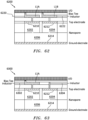
- the membrane comprising the nanopores may, in some embodiments, have a trilayer configuration, with a metal surface on either side of an insulating core material, e.g. a silicon nitride membrane.
- the metal surfaces are configured, e.g., by lithographic means, to provide a microcircuit with paired electrodes, one at each end of each nanopore, e.g., such that a current flows across the nanopore may be established between the electrodes and through the nanopore via an electrolyte media, which current can draw the polymer through the nanopore and by reversing the polarity, can draw it back.
- the electrodes can measure the change in electric potential across the nanopore so as to identify the sequence of monomers in the polymer.
- the sequence of the polymer is designed to store data.
- the data is stored in a binary code (1's and 0's).
- each base corresponded to a 1 or 0.
- an easily recognized sequence of two or more bases corresponds to a 1 and another easily recognized sequence of two or more bases corresponds to a 0.
- the data can be stored in a ternary, quaternary or other code.
- the polymer is DNA, for example single stranded DNA, wherein the DNA contains only two base types and does not contain any bases capable of self-hybridizing, e.g., wherein the DNA comprises adenines and guanines, adenines and cytosines, thymidines and guanines, or thymidines and cytosines.
- the two bases may be interspersed with one or more additional bases, for example A and C may contain a T to "punctuate" the sequence, e.g., by indicating a break in a coding sequence, at a frequency that does not result in significant self-hybridization.
- some or all available bases may be employed.
- the nucleotide bases may be natural or may in some teachings consist of or include nonnatural bases, e.g. as described in Malyshev, D. et al. "A semi-synthetic organism with an expanded genetic alphabet", Nature (2014) 509: 385-388 .
- the data is stored by addition of single monomers, e.g., single nucleotides in the case of DNA, to the polymer.
- the polymer is DNA and the monomers are adenine (A) and cytosine (C) residues.
- a and C residues have an advantage because (i) A and C have a large size difference, so differentiation through the nanopore should be facilitated, (ii) A and C do not pair with one another so do not form significant secondary structure which could complicate interpretation of the nanopore signal, and (iii) for the same reason, G's are less preferred as they are known to form guanine tetrads.
- Nucleotides are added by terminal transferase (or polynucleotide phosphorylase), but the nucleotides are 3'-blocked so that only a single nucleotide is added at a time. The block is removed prior to addition of the next nucleotide.
- the DNA is left in the nanochip. In other teachings, it is removed, and optionally converted to double stranded DNA and/or optionally converted to crystalline form, e.g. to enhance long term stability. In still other teachings, DNA can be amplified and the amplified DNA removed for long term storage, while the original template DNA, for example DNA bound to the wall of a chamber in the nanochip, can be left in the nanochip, where it can be read and/or used as a template to make additional DNA.
- the DNA or other polymer is anchored to a surface proximate to the nanopore during synthesis.
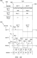
- single stranded DNA molecules may be each attached at the 5' end to a surface proximate to a nanopore, wherein the current at each nanopore can be independently regulated by electrodes for that nanopore, so that the 3'end of the DNA molecule can be pulled forward through the nanopore from a retaining chamber into a flow chamber containing a flow of 3'-protected dNTPs together with a polymerase or terminal transferase enzyme to add a 3'-protected dNTPs, or retained in the retaining chamber where the nanopore excludes the enzyme, so that the dNTP is not added.
- single stranded DNA is built by addition to the 5' end (with the 3' end attached), using topisomerase, as described more fully below.
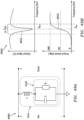
- Nanopore 1 and Nanopore 2 in this schematic are associated with different DNA strands and the positions of which (in or out of the flow chambers) are separately controllable.
- the DNA can be deprotected either by a specific enzyme in the retaining chamber, or by changing the flow in the flow chamber to provide deprotection by enzymatic, chemical, light-catalyzed or other means.
- the deblocking agent(s) flow between cycles of Flow A and Flow C, e.g., when the flow chamber is being washed with buffer, so that the deblocking agent does not deprotect the nucleotide building blocks.
- the deprotecting agent(s) are too bulky to cross to the flow chamber via the nanopores.
- the chamber configuration is similar, but with double stranded DNA anchored to the surface proximate to a nanopore, and oligonucleotide fragments, for example of two or more types, each corresponding to a binary code, are added sequentially, e.g., using site-specific recombinases, i.e., enzymes that spontaneously recognize and cleave at least one strand of a double strand of nucleic acids within a sequence segment known as the site-specific recombination sequence, for example using topoisomerase-charged oligonucleotides as described below.
- site-specific recombinases i.e., enzymes that spontaneously recognize and cleave at least one strand of a double strand of nucleic acids within a sequence segment known as the site-specific recombination sequence, for example using topoisomerase-charged oligonucleotides as described below.
- the electrically charged polymer e.g., DNA
- the charged polymer e.g., single or double stranded DNA
- bound to a surface proximate to a nanopore This can be accomplished in various ways.
- the polymer is localized to the nanopore by attaching the polymer to a relatively bulky structure (e.g.
- a bead, a protein, or a DNA origami structure (described below), having a diameter too large to fit through the nanopore, e.g., >10nm, e.g., about 20-50nm), pulling the charged polymer through the nanopore using current, anchoring the end of the polymer distal to the bulky structure to the surface adjacent to the nanopore, for example wherein the surface is modified to accept a linker group attached to the distal end of the polymer strand, thereby attaching the polymer strand, and cleaving off the bulky structure.
- the step of anchoring the end of the polymer distal to the bulky structure to the surface adjacent to the nanopore can be accomplished in various ways.
- the polymer is a single stranded DNA, and there are pre-attached DNA strands (about 50bp) which are complementary to part of the single stranded DNA, so that the single stranded DNA and the pre-attached DNA strands can join via base pairing. If the pairing is strong enough, it will be sufficient to keep the DNA anchored even while being manipulated.
- An advantage of this method of attachment is that it allows the DNA to be removed from the nanopore chip if desired for long term storage of the DNA.
- the strand is attached to the surface covalently, either using conjugation chemistry, e.g., streptavidin-biotin conjugation as described in Example 1 below, or 'click' chemistry (see Kolb, et al. Angew. Chem. Int. Ed. (2001)40: 2004-2021 , and/or using enzymatic attachment, for example by pre-attaching oligos covalently to the distal surface, and then using DNA ligase to connect them.
- conjugation chemistry e.g., streptavidin-biotin conjugation as described in Example 1 below
- 'click' chemistry see Kolb, et al. Angew. Chem. Int. Ed. (2001)40: 2004-2021
- enzymatic attachment for example by pre-attaching oligos covalently to the distal surface, and then using DNA ligase to connect them.
- the bulky structure is cleaved off, e.g., using an endonuclease which cleaves at a restriction site near the bulky structure.
- the bulky structure may be a bead, a bulky molecule, e.g., a protein which is reversibly bound to a DNA strand, or a DNA origami structure.
- DNA origami involves the use of base pairing to create three dimensional DNA structures. DNA origami techniques are generally described in Bell, et al, Nano Lett. (2012)12: 512-517 .
- DNA origami can be used to attach the single DNA molecule to a surface adjacent to the nanopore.
- the structure is a ⁇ honey comb cube', e.g., about 20nm on each side. This prevents this part of the DNA from going through the nanopore (just like in the attached paper).
- the electrically charged polymer, e.g., DNA, with the origami structure is in the middle chamber of a three chamber configuration.
- the origami will keep the DNA from completely entering the other 2 chambers (or other one chamber in the 2 chamber example).
- the polymer doesn't need to be anchored to the surface. This reduces the risk that the polymer will knot up and avoids the need for the step of binding one end of the polymer to the surface and cleaving off the bulky portion at the other end.
- the volume of the chamber with the origami should be kept as small as practical so that the polymer stays relatively close to the pore, which will help ensure that it translocates quickly when current is applied.
- middle chamber containing the origami portion of the polymer can't be interconnected with other middle chambers (or else the different polymers will get mixed up), the other chambers (or sets of chambers in the 3 chamber example) can be interconnected. These other chambers can have larger volumes if desired, as the polymer will necessarily be close to the pore (some of it will be in the pore in fact) when the DNA is moved to that chamber.
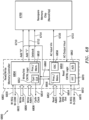
- the device comprises three in-line chambers, wherein the addition chambers are contiguous to allow for flow, and have common electrodes, while the ⁇ deprotect' chambers are fluidically isolated except for the flow through the nanopore and have unique electrodes.
- the DNA or other charged polymer is not anchored but can move between synthesis chamber(s) and deprotection chamber(s), under control of electrodes in the chambers, while the polymerase and the deprotecting agents are restricted from movement between chambers because they are too bulky to pass through the nanopores connecting the chambers and/or are anchored to a surface in a chamber. See, e.g., Figures 1-9 and 16-17 .
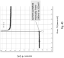
- the current needed to move the charged polymer through the nanopore depends on, e.g., the nature of the polymer, the size of the nanopore, the material of the membrane containing the nanopore, and the salt concentrations, and so will be optimized to the particular system as required.
- examples of voltage and current would be, e.g., 50-500mV, typically 100-200mV, and 1-10nA, e.g., about 4nA, with salt concentrations on the order of 100mM to 1M.
- the movement of charged polymer, e.g., DNA, through the nanopore is normally very rapid, e.g., 1 to 5 ⁇ s per base, so on the order of one million bases per second (1 MHz, if we adopt the nomenclature of frequency), which presents challenges for getting an accurate reading distinct from the noise in the system.
- a nucleotide needed to be repeated in a sequence e.g., ca.
- the charged polymer is a nucleic acid, e.g., single stranded DNA, wherein the sequences provide a secondary structure.
- Bell, et al., Nat Nanotechnol.(2016)11(7):645-51 describes using a relatively short sequence of dumbbell configurations detectible in a solid state nanopore format, to label antigens in an immunoassay.
- the nanopores used in Bell, et al. were relatively large, so the entire dumbbell structure could pass through the pore, but using nanopores smaller than the diameter of the dumbbell configuration, the DNA will "unzip" and become linearized. More complex configurations can be used, e.g.
- each bit corresponds to a sequence similar to a tRNA (see, e.g., Henley, et al. Nano Lett. (2016)16:138-144 ).
- the present disclosure uses charged polymers, e.g. single stranded DNA, having at least two types secondary structure, wherein the secondary structure encode data (e.g. binary data, wherein one secondary structure type is a 1 and a second is a 0).
- secondary structures are used to slow down the passage of the DNA through the nanopore or to provide breaks in the sequence, to facilitate reading of the sequence.
- the present disclosure utilizes a DNA molecule comprising a series of at least two different DNA motifs, wherein each motif specifically binds to a particular ligand, for example a gene regulatory protein for double stranded DNA or a tRNA for single stranded DNA, wherein the at least two different DNA motifs encode information, e.g. in a binary code, wherein one motif is a 1 and a second is a 0, e.g., wherein the ligand enhances the signal difference (e.g. change in current or capacitance) across the nanopore as the DNA passes through the nanopore.
- a particular ligand for example a gene regulatory protein for double stranded DNA or a tRNA for single stranded DNA
- the at least two different DNA motifs encode information, e.g. in a binary code, wherein one motif is a 1 and a second is a 0, e.g., wherein the ligand enhances the signal difference (e.g. change in current or capacit
- capacitance exists in any circuit where there is a gap between one electrical conductor and another. While current varies directly with capacitance, it does not vary simultaneously with capacitance. For example, if we were to plot the current and voltage over time in a capacitive circuit with an alternating electrical current, we would see that while both current and voltage each form a sine wave, the waves are out of phase. When there is a change in current, there is a change in capacitance, which is reflected in a change in the phase of the signal.
- a radiofrequency alternating current provides a signal with fixed frequency and amplitude, while the phase of the signal will vary with the capacitance of the circuit.
- a pulsating direct current rather than an alternating current (i.e., the voltage alternates between two values, but the voltage does not cross the "zero" line, such that polarity is maintained and one electrode remains positive and the other negative), so that the charged polymer can be drawn through the nanopore (towards the positive electrode in the case of DNA).
- the capacitance has one value, which changes as the different monomers of the polymer pass through the nanopore.
- Suitable frequency ranges are in the radiofrequency range, e.g. 1 MHz to 1GHz, e.g. 50-200MHz, for example about 100MHz, e.g. below higher microwave frequencies that could cause significant dielectric heating of the medium.
- different frequencies can be applied at different nanopores so that multiple nanopores can be measured simultaneously with a single radiofrequency input line.
- Measuring impedance changes due to, e.g. changes in capacitance
- Using a high frequency signal enhances the signal-to-noise ratio, as many measurements are made within a given time span, providing a more stable signal which is readily distinguished from impedance changes due to environmental or device variation and fluctuation.
- the present invention provides a method of measuring an impedance change in a high frequency signal induced by a change in capacitance as monomers (e.g., nucleotides) pass through a nanopore, a method of reading a monomer sequence of a charged polymer comprising at least two different types of monomers, for example a DNA molecule, comprising applying a radiofrequency pulsating direct current, e.g. at a frequency of 1 MHz to 1GHz, e.g.
- a nanopore-based cell 4800 having an upper (or top) chamber 4802 and a lower (or bottom) chamber 4804 and a membrane 4806, which separates the two chambers 4802, 4804.
- the membrane is made of a material as described herein above.
- a nanopore 4808 (or nanometer-sized hole) through the membrane, having a shape and dimensions such at that described herein, which allows for fluid communication between the chambers 4802, 4804.
- a polymer molecule e.g., a single-stranded DNA molecule 4810 (or ssDNA), such as that described herein above.
- the DNA 4810 has three units or bases, an upper base 4812, a middle base 4814, and a lower base 4816.
- Each of the bases 4812-4816 in the DNA 4810, or a collection of bases, may be referred to as a "bit" of information used to represent or store data, as also discussed herein. Any other polymer or DNA molecule (single or double-stranded) may be used if desired, as discussed herein above.
- the chambers 4802, 4804, of the cell 4800 may be filled with a fluid, such as that describe herein, that allows the DNA 4810 to float and move between the chambers 4802,4804.
- the cell 4800 also has a pair of electrodes 4818, 4820, an upper (or top) electrode 4818 connected to an input voltage Vin, and a lower (or bottom) electrode 4820 connected to ground (or GND or 0 volts).
- the lower electrode 4820 may also be connected to a non-zero DC voltage, but may still be at AC (or rf or radio frequency) "ground” through use of an AC coupling capacitor, connected to the electrode, having a capacitance value which passes the AC voltage (discussed more hereinafter).
- Voltage applied to the electrodes 4818,4820 determines the movement of the DNA 4810 in the cell 4800.
- the DNA 4810 will be attracted to the positive charge or voltage, because the DNA molecule 4810 has a net negative charge, as described hereinbefore with Figs. 1-5 .
- Figs. 48A, 48B and 48C shows the DNA 4810 moving through the nanopore 4808 from the upper chamber 4802 to the lower chamber 4804.
- the cell 4800 (or the nanopore and DNA system) may be electrically modeled as an equivalent circuit diagram 4830, shown as a capacitor C1 and resistor R1 connected in parallel.
- the top electrode 4818 sees a capacitance C1 and resistance R1 to ground that is set by its local environment, where the capacitor C1 represents the capacitance of the cell 4800 as determined by the properties of the two electrodes 4818,4820 (i.e., the capacitor plates) and the properties of dielectric material there-between, defined at least by the fluid within the cell 4800 and the membrane 4806 with the nanopore 4808.
- the resistor R1 represents the DC resistance associated with the cell 4800, defined at least by the losses associated with the dielectric material of the cell described above, which appear as a DC leakage current between the two electrodes.
- both the cell capacitance and resistance changes.
- Different DNA bases have different sizes, and thus have different effects on the capacitance and resistance, resulting in different equivalent circuit models as illustrated in Figs 48A-48C .
- the DNA 4810 is outside the nanopore 4808, resulting in a set of values C1,R1 (or Zcell1).
- the base 4814 of the DNA 4810 is in the nanopore, resulting in another set of values C2,R2 (or Zcell2).
- the base 4812 of the DNA 4810 is in the nanopore, resulting in another set of values C3,R3 (or Zcell3).
- the capacitance C and resistance R of the cell 4800 are combined with an inductor L to create an "inductor-cell” or “cell-inductor” RLC resonant circuit or resonator or filter (or band-stop, or notch, or band-reject filter) as shown by the circuit 4900 ( Fig. 49A ), having a magnitude frequency response shown by a graph 4952, and a phase frequency response shown by a graph 4954.
- the magnitude response 4952 of the resonant circuit 4900 (for a given value of C and R) has maximum attenuation (minimum impedance) at the resonant frequency f res , and a steep magnitude attenuation response over a narrow frequency band (or stop band) ⁇ f stp around the resonant frequency f res , which is the frequency range over which the magnitude response (Vout/Vin) is below a standard threshold, e.g., 3dB (or 20Log[SQRT(2)]).
- a standard threshold e.g., 3dB (or 20Log[SQRT(2)]
- the corresponding phase shift response curve 4954 of the resonant circuit 4900 has a phase shift of 45 degrees at the resonant frequency f reg (when the reactance or imaginary portion of the complex impedance is equal to zero), and has a steep phase response over the narrow stop band ⁇ f stp on each side of the resonant frequency f res , such that at frequencies above f reg and outside the band ⁇ f stp , the phase shift is at or near 180 deg., and at frequencies below f reg and outside the band ⁇ f stp , the phase shift is at or near 0 deg. Otherwise, the phase response output is substantially constant and non-shifting over all other frequencies.
- a family of resonant frequency response magnitude curves 5002 and phase curves 5003 of the resonant circuit (or filter) are shown in response to DNA (or other polymer or molecule having varying sizes along its length) passing through a nanopore and changing the capacitance (or impedance) measured to ground (e.g., 0 volts), and thereby changing the resonant frequency f res , as shown by the magnitude response curves 5010-5018 and the corresponding phase response curves 5020-5028.
- Eq. 2 increasing the capacitance measured to ground, decreases the resonant frequency f res .
- f res when DNA is in the nanopore, f res would be lowest when the largest base, e.g., Base G, is in the nanopore and f reg would be the highest when the smallest base, e.g., Base C, is in the nanopore. Also, when the nanopore is open (unblocked), i.e., no DNA or polymer in the nanopore, f res would be the highest frequency. This range or band of resonant frequencies is shown as ⁇ f res in Fig. 50 . Also, for the resonator response curves 5010-5018 for magnitude and 5020-5028 for phase shown in Fig. 50 , the overall bandwidth of the resonator (over which magnitudes and phase are materially affected by the resonator) is shown in Fig. 50 as ⁇ f BW .
- the overall resonant frequency band ⁇ f res for a given cell-inductor resonant circuit (or resonator or filter), presuming all other cell conditions affecting impedance remained fixed, would have a maximum resonant frequency f res-max when the nanopore is open (or unblocked by the polymer), and a minimum resonant frequency f res-min when the nanopore is closed (or blocked by the polymer), and the cell resonant frequency f reg is varied (or tuned or changed) by the size of the polymer in the nanopore at a given time, and thus may be referred to herein as a nanopore-polymer resonator (or NPR).
- the overall bandwidth ⁇ f Bw of the resonator (over which magnitudes and phase are materially affected by the resonator) would similarly be determined based on the resonant frequency band ⁇ f res .
- the resonator When there is an AC voltage applied to the resonator and the output voltage signal (Vout) of the resonator is observed (or monitored) at a fixed frequency f probe , e.g., near the center of the resonant frequency range for the DNA bases shown, shown as a dashed vertical line 5004, not necessarily aligned with one of the center (or resonant) frequencies f reg , the resonator provides four different possible output signals (or magnitude attenuation or phase shift amounts) at that frequency f probe , depending on the specific DNA base (size) passing through the nanopore, and a fifth output voltage state when the DNA is not in the nanopore ("open pore" condition). These five output signals are shown by where the family of response curves 5002,5003 intersect with the line 5004 corresponding to the monitor frequency f probe , i.e., magnitudes V1-V5, and phases Ph1-Ph5.
- the output voltage at the frequency f probe2 would be five magnitude output voltages V6-V10 (different from the output voltages V1-V5 seen at f probe ) and five output phase shifts Ph6-Ph10 (different from the output voltages Ph1-Ph5 seen at f probe ).
- these different five output signals are shown by where the family of response curves 5002, 5004 intersect with the line 5006 corresponding to the monitor frequency f probe2 , i.e., magnitudes V6-V10, and phases Ph6-Ph10.
- the values of V1-V10 and Ph1-Ph10 are arbitrary designations and are used for identification or labeling purposes only.
- the value or location for the probe or monitoring frequency f probe , f probe2 may be set based on the desired response values, as described below. As shown below, using values for the probe or monitoring frequencies in the range of resonant frequencies seen when the polymer is in the nanopore, may provide a useful range of output values. Other measurement or probe frequencies may be used if desired provided it meets the desired functional and performance requirements.
- the resonant frequency f res will be the lowest (capacitance highest), and the corresponding response is shown by the (far left) magnitude and phase curves 5010, 5020, respectively.
- the output voltage at the frequency f probe where the curves 5010, 5020 intersect with the line 5004 would correspond to an output voltage V2 and output phase Ph1, respectively.
- the output voltage at the frequency f probe2 where the curves 5010, 5020 intersect with the line 5006 would correspond to an output voltage V10 and output phase Ph6, respectively.
- the resonant frequency f res will be a little higher than that of the previous base, and the response is shown by the magnitude and phase curves 5012, 5022, respectively.
- the output voltage at the frequency f probe where the curves 5012, 5022 intersect with the line 5004 would correspond to an output voltage V5 and output phase Ph2, respectively.
- the output voltage at the frequency f probe2 where the curves 5012, 5022 intersect with the line 5006 would correspond to an output voltage V9 and output phase Ph7, respectively.
- the resonant frequency f res will be a little higher than that of the previous base, and the response is shown by the magnitude and phase curves 5014, 5024, respectively.
- the output voltage at the frequency f probe where the curves 5014, 5024 intersect with the line 5004 would correspond to an output voltage V4 and output phase Ph3, respectively.
- the output voltage at the frequency f probe2 where the curves 5014, 5024 intersect with the line 5006 would correspond to an output voltage V8 and output phase Ph8, respectively.
- the resonant frequency f res When the smallest base (e.g., Base C) passes through the nanopore, the resonant frequency f res will be a little higher than that of the previous base, and the response is shown by the magnitude and phase curves 5016, 5026, respectively.
- the output voltage at the frequency f probe where the curves 5016, 5026 intersect with the line 5004 would correspond to an output voltage V3 and output phase Ph4, respectively.
- the output voltage at the frequency f probe2 where the curves 5016, 5026 intersect with the line 5006 would correspond to an output voltage V7 and output phase Ph9, respectively.
- the resonant frequency f reg will be the highest (capacitance lowest), and the response is shown by the magnitude and phase curves 5018, 5028, respectively.
- the output voltage at the frequency f probe where the curves 5018, 5028 intersect with the line 5004 would correspond to an output voltage V1 and output phase Ph5, respectively.
- the output voltage at the frequency f probe2 where the curves 5018, 5028 intersect with the line 5006 would correspond to an output voltage V6 and output phase Ph10, respectively.
- a DNA-reading time sequence 5100 in accordance with embodiments the present disclosure is shown for reading data stored in DNA using two-bits (e.g., two bases) in the DNA strand 4810 via the "inductor-cell" resonator or “capacitive-resonance" DNA data reading technique of the present disclosure measured at a fixed probe (or monitor) frequency f probe .
- the DNA-reading time sequence has 5 time segments or stages T1-T5, shown as five columns 5102 to 5110, and the progression between time segments is shown by dashed lines 5111. For each of the time stages T1-T5, there is an image showing the DNA 4810 ( Fig.
- magnitude and phase response curves 5112-5120 for the time stages T1-T5, respectively, showing the intersection of the response curve at the monitor frequency f probe (corresponding to a curve from the family of curves shown in Fig. 50 ), and two output value graphs 5130, 5132 showing corresponding output signals (e.g., voltage values) for the magnitude and phase responses, respectively, at the monitor frequency f probe across each of the time stages T1-T5.
- the values V1-V5 and Ph1-PH5 for the graphs 5130, 5132 may be any voltage values indicative of the output value for that parameter having the appropriate range and scaling to provide the functions described herein.
- the DNA 4810 is outside of the pore 4808, the capacitance to ground is low (as discussed herein), the resonance frequency f reg is high, and the measured magnitude output signal is high and the phase value is very low (e.g., about 0 deg.) at the monitoring frequency f probe , which corresponds to the response curves 5018, 5028 shown in Fig. 50 , having output values at f probe where the curves 5018, 5028 intersect with the line 5004, corresponding to an output voltage V1 and output phase Ph5, respectively.
- the DNA base 4816 (Base A, in this example) enters the pore 4808, the capacitance to ground increases, the resonance frequency f reg shifts to lower central frequency, and the measured magnitude output signal is low and the phase value is intermediate (e.g., about 90 deg.) at f probe , which corresponds to the response curves 5012, 5022 shown in Fig. 50 , having output values at f probe where the curves 5012, 5022 intersect with the line 5004, corresponding to an output voltage V5 and output phase Ph2, respectively.
- Base A in this example
- the DNA base 4814 (Base G, the largest base, in this example), enters the pore 4808, the capacitance to ground extremely high, and the resonance frequency f res shifts lower, but the magnitude output signal is an intermediate output value is upper-mid (e.g., about 135 deg.) at f probe , which corresponds to the response curves 5010, 5020 shown in Fig. 50 , having output values at f probe where the curves 5010, 5020 intersect with the line 5004, corresponding to an output voltage V2 and output phase Ph1, respectively.
- Base G the largest base, in this example
- the DNA base 4812 (Base A in this example) enters the pore 4808 (again), the capacitance to ground decreases (from the value at T3), the resonance frequency f res shifts to central frequency, and the measured magnitude output signal is low and the phase value is intermediate (e.g., about 90 deg.) at f probe , which corresponds to the response curves 5012, 5022 shown in Fig. 50 , having output values at f probe where the curves 5012, 5022 intersect with the line 5004, corresponding to an output voltage V5 and output phase Ph2, respectively.
- the phase value is intermediate (e.g., about 90 deg.) at f probe , which corresponds to the response curves 5012, 5022 shown in Fig. 50 , having output values at f probe where the curves 5012, 5022 intersect with the line 5004, corresponding to an output voltage V5 and output phase Ph2, respectively.
- the DNA 4810 is outside of the pore 4808 (again), the capacitance to ground is low, the resonance frequency f res shifts (again) to high frequency, and the measured magnitude output signal is high at f probe , which corresponds to the response curves 5018, 5028 shown in Fig. 50 , having output values at f probe where the curves 5018, 5028 intersect with the line 5004, corresponding to an output voltage V1 and output phase Ph5, respectively.
- FIG. 52 another overview example 5200 of a time sequence (T1-T5) is shown for reading data stored in DNA using two-bits (e.g., two bases) in the DNA strand via the capacitive-resonance DNA data reading technique of the present disclosure using a different fixed probe (or monitor) frequency f probe2 .
- the sequence has 5 time segments or stages T1-T5, shown as five columns 5202-5210, and the progression between time segments is shown by dashed lines 5211. For each of the time stages T1-T5, there is an image showing the DNA 4810 ( Fig.
- magnitude and phase response curves 5212-5220 for the time stages T1-T5, respectively, showing the intersection of the response curve at the monitor frequency f probe2 (corresponding to a curve from the family of curves shown in Fig. 50 ), and two value graphs 5230, 5232 showing corresponding output signals (e.g., voltage values) for magnitude and phase responses, respectively, at the monitor frequency f probe2 across each of the time stages T1-T5.
- the values V1-V5 and Ph1-PH5 for the graphs 5130, 5132 may be any voltage values indicative of the output value for that parameter having the appropriate range and scaling to provide the functions described herein.
- the DNA 4810 is outside of the pore 4808, the capacitance to ground is low (as discussed herein), the resonance frequency f reg is high, and the measured magnitude output signal is high and the phase shift value is very low (e.g., about 0 deg.), which corresponds to the response curves 5018, 5028 shown in Fig. 50 , having output values at f probe2 where the curves 5018, 5028 intersect with the line 5006, corresponding to an output voltage V6 and output phase Ph10, respectively.
- the DNA base 4816 (Base A, in this example) enters the pore 4808, the capacitance to ground increases, the resonance frequency f res shifts to lower central frequency, and the measured magnitude output signal is intermediate and the phase value is low-mid value (e.g., about 45 deg) at f probe2 , which corresponds to the response curves 5012, 5022 shown in Fig. 50 , having output values at f probe2 where the curves 5012, 5022 intersect with the line 5006, corresponding to an output voltage V9 and output phase Ph7, respectively.
- Base A in this example
- the DNA base 4814 (Base G, the largest base, in this example), enters the pore 4808, the capacitance to ground is extremely high, and the resonance frequency f res shifts lower, and the magnitude output signal at f probe2 is at a low output value and the output phase is at about an intermediate or mid value (e.g., about 90 deg.), which corresponds to the response curves 5010, 5020 shown in Fig. 50 , having output values at f probe2 where the curves 5010, 5020 intersect with the line 5006, corresponding to an output voltage V10 and output phase Ph6, respectively.
- Base G the largest base, in this example
- the DNA base 4812 (Base A, in this example) enters the pore 4808 (again), the capacitance to ground decreases (from value at T3), the resonance frequency f res shifts to central frequency, and the measured magnitude output signal is intermediate and the phase is low at f probe2 , which corresponds to the response curves 5012, 5022 shown in Fig. 50 , having output values at f probe2 where the curves 5012, 5022 intersect with the line 5006, corresponding to an output voltage V9 and output phase Ph7, respectively.
- the DNA 4810 is outside of the pore 4808, the capacitance to ground is low, the resonance frequency f res shifts to a higher frequency, and the measured magnitude output signal is high and the phase signal is very low (e.g., about 0 deg.) at f probe2 , which corresponds to the response curves 5018, 5028 shown in Fig. 50 , having output values at f probe2 where the curves 5018, 5028 intersect with the line 5006, corresponding to an output voltage V6 and output phase Ph10, respectively.
- the desired output values can be selected based on the measurement or monitoring frequency f probe , f probe2 .
- any number of “bits” may be used if desired for the data storage polymer, provided the change in cell capacitance or impedance (and corresponding resonance frequency, or frequency response) is sufficient to produce an output magnitude and/or phase for each bit that is distinguishable over each of the other bits.
- capacitance change may be accomplished by changing the physical molecular size of the bases (e.g., the diameter)
- any property of the bases that creates a unique capacitance value of the cell when passing through the nanopore may be used if desired.
- bases that have different dielectric properties, different ionic (or charge) properties, and/or different quantum mechanical/electricalproperties may be used, provided they meet the desired functional and performance requirements.
- FIG. 53 an equivalent circuit and block diagram 5300 of a DNA data reading network array of the present disclosure is shown, having a parallel array of resonant circuits or Nanopore Polymer Resonators (NPRs) 5302-5306 (NPR1-NPR3) each connected in parallel, through a individual coupling capacitors C CPL (discussed hereinafter), to a common AC input voltage source 5308, which provides an AC voltage Vin having a frequency that includes at least the desired measurement frequency(ies) (f probe ) for each of the resonant circuits NPR1-NPR3 (discussed more hereinafter).
- NPRs Nanopore Polymer Resonators
- Each of the resonators NPR1-NPR3 has a unique inductor values L1-L3, respectively, connected in series with equivalent circuits 5312-5316 of corresponding cells (similar to the cell 4800 described in Figs. 48A-48C , and similar to the equivalent circuit 4900 described in Fig. 49A ), having a variable capacitor C and variable resistor R, which vary based on the location of the polymer (or DNA) 4810 ( Fig. 48A ) in the cell 4800 with respect to the nanopore 4808 in the cell 4800 (as discussed herein above).
- Each of the unique inductor values L1-L3 sets a unique resonant frequency band ⁇ f reg ( Fig.
- the plurality of resonators NPR1-NPR3 are connected in parallel in a frequency-multiplexed (or frequency-division multiplexed) arrangement creating an array of the resonators NPR1-NPR3, all driven by a single AC input voltage 5308, and each responding to its own probe input frequency.
- an optional AC RF attenuator 5310 may be provided in series with the AC input source 5308 prior to the connection to the parallel array of resonators NPR1-NPR3 to provide a voltage divider or impedance matching with the resonators NPR1-NPR3 and/or to adjust the AC output voltage Vout range based on the range of impedance values of the resonators over the operational frequency range of interest.
- the attenuator 5310 may be a constant or switched or variable type RF attenuator, depending on the frequency range used, the impedance of the array and load, and/or the desired functional and performance characteristics.
- an AC output voltage Vout from the parallel array of resonators NPR1-NPR3 may be provided to an amplifier (or pre-amp) 5320, which performs signal conditioning on the output signal Vout, such as remove noise, filter around the measurement frequency(ies) of interest, isolate impedance of resonator array from down-stream devices or components, improve measurement sensitivity, amplify or attenuate the Vout signal, and/or perform other desired signal conditioning of the AC output voltage signal Vout as needed to provide the desired functions and/or performance.
- the amplifier may also be an active filter which filters the AC output voltage signal around one or more of the probe frequencies.
- the amplifier 5320 provides an analog AC conditioned output voltage Vout signal on line 5322 to an A/D Converter 5324 (e.g., an integrated circuit or chip), which digitally samples the conditioned AC output voltage Vout and provides digital output data on a line 5326 indicative of the sampled conditioned AC output voltage Vout signals.
- A/D Converter 5324 e.g., an integrated circuit or chip
- the sample rate of the A/D converter may be any rate that provides sufficient sampling of the output signal to preserve the ability to perform frequency analysis at the desired measurement frequencies (e.g., the probe frequencies).
- the AC output voltage may also be down-converted to a lower intermediate frequency or DC, e.g., if the fundamental probe frequency(ies) is/are too high (or fast) to be directly sampled accurately by the A/D converter (or for other design or performance reasons), by mixing the AC output signal with the same (or similar) frequency, e.g., homodyne or heterodyne demodulation, or any other type or demodulation or frequency conversion, provided it preserves the magnitude and/or phase components needed to accurately measure the desired parameters.
- the A/D converter 5324 may have on-board memory that stores the sampled output data and/or may be connected to or communicate with a separate memory device (not shown) which may store all or a portion of the sampled output data.
- the digital sampled output data is provided on the line 5326 to digital signal processing frequency analysis (or decomposition) logic 5328, such as an FFT (or Fast Fourier Transform) logic or chip, which performs digital signal processing (DSP) on the digital sampled data and provides digital data on a line 5330 indicative of the magnitude and/or phase of the frequency components (or harmonics) that exist in the sampled AC output signal Vout.
- digital signal processing frequency analysis logic 5328 such as an FFT (or Fast Fourier Transform) logic or chip, which performs digital signal processing (DSP) on the digital sampled data and provides digital data on a line 5330 indicative of the magnitude and/or phase of the frequency components (or harmonics) that exist in the sampled AC output signal Vout.
- FFT Fast Fourier Transform
- any other frequency analysis hardware, firmware and/or software may be used if desired, provided it provides the functions and performance described herein and adequately measures the magnitude and/or phase of the output signal at the desired frequencies of interest (e.g., at least at the desired probe or
- the amplifier 5320, the A/D converter 5324, and the FFT logic 5329 are all known hardware or firmware components (which may have computer programmable portions) that may be obtained from an integrated circuit provider, such as Texas Instruments, Inc., Analog Devices, Inc., National Instruments Corp., Intel Corp, or other similar manufacturers.
- an integrated circuit provider such as Texas Instruments, Inc., Analog Devices, Inc., National Instruments Corp., Intel Corp, or other similar manufacturers.
- One example of components for digitization include: Xilinx FFT LogiCORE, part no. 4DSP FMC103, 1126, Alazartec 9360, 9370. Other components may be used if desired, provided they provide the functions and performance described herein.
- the FFT logic may be performed by a field programmable gate array (FPGA).
- the output signal Vout may be provided to one or more analog filters (not shown) tuned to the desired frequencies to identify the magnitude and/or phase of the desired frequency components and provide an analog output voltage signal indicative of same.
- a frequency plot 5400 shows a sample frequency separation for the plurality of resonators NPR1-NPR3 of Fig. 53 of the present disclosure.
- each of the resonators NPR1-NPR3 has a unique resonator bandwidth ⁇ f BW1 , ⁇ f BW2 , ⁇ f BW3 , which are set or determined by the unique inductor values L1-L3, respectively.
- the bandwidths ⁇ f BW1 , ⁇ f BW2 , ⁇ f BW3 , of the resonators NPR1-NPR3, respectively, may be separated from adjacent resonator bandwidths by a frequency separation or gap ⁇ f gap such that the resonator bandwidth ⁇ f BW of adjacent resonators do not overlap and cause interference or cross-talk between the adjacent resonators.
- the bandwidths may overlap provided the frequency response of each base is different and thus, they do not affect the ability to identify the response of each resonator.
- Fig. 54 there is shown a set of probe or monitor frequencies f p1 ,f p2 ,f p3 corresponding to the bandwidths ⁇ f BW1 , ⁇ f BW2 , ⁇ f BW3 , of the resonators NPR1-NPR3, respectively, which may be a frequency (or frequencies) within each of the resonator bandwidths ⁇ f BW1 , ⁇ f BW2 , ⁇ f BW3 , that provides the desired output signals as discussed herein, such as in the range of resonant frequencies seen when the polymer is in the nanopore (as discussed herein above with Figs. 50-52 ).
- Other measurement or probe frequencies may be used if desired provided it meets the desired functional and performance requirements.
- the gap frequency is determined primarily by the choice of inductor L value
- the amount of separation between adjacent frequency bands needed to avoid undesired overlap during operation caused by system parameter variations that may occur over the system operating conditions may also be determined by various factors, including but not limited to cell design parameter tolerances (e.g., electrodes, inductors, capacitors, fluids, cell walls, membranes, materials, dimensions, and any other cell design parameters that may vary from cell to cell), environmental operating ranges, e.g., temperature, pressure, humidity, and the like, electromagnetic interference or noise parameters/effects, any cell-to-cell (or chamber-to-chamber) interactions, and/or any other design practice, safety or regulatory requirements or tolerances, or any other factors that may affect the desired function or performance.
- cell design parameter tolerances e.g., electrodes, inductors, capacitors, fluids, cell walls, membranes, materials, dimensions, and any other cell design parameters that may vary from cell to cell
- environmental operating ranges e.g., temperature, pressure, humidity, and
- the AC input voltage Vin of the present disclosure includes at least desired measurement or probe frequencies at which the output AC voltage Vout will be frequency analyzed (e.g., by the FFT logic 5330 - Fig. 53 ).
- the AC input voltage Vin may be a continuous broadband AC frequency signal shown by a curve 5502 having all frequencies from the minimum possible measurement frequency f MIN to the minimum possible measurement frequency f MAX , or from the first probe frequency f p1 to the last probe frequency f pN . In that case, all the resonators NPR1-NPR3 are excided by the broadband frequency signal and will exhibit a response in the frequency components of the output signal.
- the AC input voltage Vin may be a broadband AC frequency signal shown by a curve 5510 having only the desired probe or monitor frequencies f p1 ,f p2 ,f p3 ,f pN f as shown by the individual frequency components 5512,5514,5516, 5518, respectively.
- the overall frequency range for the AC input voltage Vin for all the resonators in the array may be from about 1.0 MHz to 1GHz. Other frequencies may be used if desired, provided it meets the function and performance described herein.
- the AC input voltage Vin may be provided by a known oscillator chip (which may be adjustable and/or programmable) that provides the desired AC frequency components for the desired design configuration and excitation, such as FMC 2850, TIDAC900, or Xilinx DS558.
- Vin may be created by combining separate AC frequencies together electronically, or directly synthesized mathematically and programmed into the oscillator (either hard wired or programmed by a microprocessor connected thereto).
- the AC input voltage Vin may be a time swept AC frequency signal shown by a curve 5550, sweeping the input frequency from the minimum possible measurement frequency f MIN to the minimum possible measurement frequency f MAX , or from the first probe frequency f p1 to the last probe frequency f pN , and then repeated having a repeat-period of time T.
- the frequency of the input voltage Vin is at only one frequency at any given time, and all the resonators NPR1 -NPR3 respond to that single input frequency and will exhibit a response to that frequency at the output signal.
- the AC input voltage Vin may be a time-stepped AC frequency signal shown by a curve 5570, where the input frequency is stepped from the first probe frequency f p1 to the last probe frequency f PN , and waits a predetermined dwell time T D at each frequency, and then is repeated having a repeat-period of time T.
- the frequency of the input voltage Vin is at only one frequency at any given time, all the resonators NPR1-NPR3 respond to that single input frequency and will exhibit a response to that frequency at the output signal at that time.
- the dwell time T D allows more time for system to sample the output signal at each probe frequency.
- the overall frequency range for the AC input voltage Vin for all the resonators (and also the probe measurement frequency) in the array may be from about 1.0 MHz to 1GHz. Other frequencies may be used if desired, provided they meet the functional and performance requirements described herein.
- the AC input frequency should be set at a value that enables sufficient number of cycles (or periods) of the input frequency to allow the impedance of the cell to be adequately sampled. This will be based in part on the speed at which the DNA (or other polymer) is moving through the nanopore.
- the cell impedance will receive (or experience) 100 cycles of the input frequency for each base, which corresponds to a 100: 1 "sample" rate.
- Other input frequencies and sample rates may be used if desired, provided they provide the desired function and performance.
- the minimum sample frequency required to digitally resolve a given input frequency is the Nyquist sample frequency, which is 2 x the input frequency. In this case, for a 1MHz input signal (rate of DNA passage through nanopore), the minimum (or Nyquist) sample rate would be 2MHz.
- Fig. 56 an example of frequency spectrum graphs of the AC output voltage Vout magnitude and phase 5600, 5620, respectively, are shown, for some embodiments of the present disclosure.
- the probe frequency used is f probe2
- NPR1 had the scenario shown in column 5206 at time T3 ( Fig. 52 ), and the corresponding frequency response line 5602 indicates a magnitude of V10 and a phase ofPh6.
- NPR2 had the scenario shown in column 5204 at time T2 ( Fig. 52 ), and the corresponding frequency response line 5604 indicates a magnitude of V9 and a phase of Ph7.
- NPR3 had the scenario shown in column 5210 at time T5 ( Fig. 52 ), and the corresponding frequency response line 5606 ( Fig. 56 ) indicates a magnitude of V6 and a phase of Ph10.
- the probe or measurement frequency used may vary based on the resonator frequency response, polymer properties, and other factors such as system noise that may affect the quality of the output signal.
- the system may switch between measurement frequencies in real time to ensure the best quality output signal is obtained, or multiple different measurement frequencies may be used to perform error checking or validation of the data read.
- the AC input frequency of Vin should include the measurement frequency, e.g., by changing or adjusting accordingly (in synch with the measurement) or having the measurement frequency be part of the continuous AC input frequency components provided.
- a top level block diagram 5700 is shown for embodiments of the present disclosure.
- the array of resonators (or NPRs) when laid-out on a chip, it may be configured in a 2-Dimensional array of MxN resonators, where there are M rows 5702-5708 and each row having N resonators, all connected in parallel (as shown by lines 5716) and all NPRs driven by the same AC input voltage Vin 5308 ( Fig. 53 ) on the line 5710 and all NPRs contributing to a common frequency division multiplexed AC output voltage Vout on a line 5712, which may be fed to the amplifier (or pre-amp) 5320 ( Fig. 53 ).
- each of the rows 5702-5708 may correspond to a frequency band, such as 100MHz-199Mhz (for row 5702), 200MHz-299MHz (for row 5704), 300Mz-399MHz (for row 5706), and the like for the other rows.
- a frequency band such as 100MHz-199Mhz (for row 5702), 200MHz-299MHz (for row 5704), 300Mz-399MHz (for row 5706), and the like for the other rows.
- resonators or NPRs
- Each of the NPRs in a given row have a resonator bandwidth ⁇ f BW within the frequency band associated with that row, and is separated in frequency from the adjacent NPR by a gap frequency band ⁇ f gap , to avoid interference or cross-talk between the adjacent resonators, as discussed herein above with Fig. 54 .
- the reading system may be viewed as a 2D array of data elements that are individually readable with a single input and output line.
- Other frequency bands and ranges may be used if desired.
- a cross-sectional view of a multi-layer chip structure 5800 is shown, including the cell 4800 ( Fig. 48A ), the inductor L ( Figs 49A , 53 ), and the coupling capacitor C CPL , and including a top contact 5802, where the input (and output) I/O voltage line may be connected, which may collectively referred to herein as the nanopore-polymer resonator (NPR).
- Matching components of the cell 4800 ( Fig. 48A ) are labeled the same in Fig. 58 .
- Above the upper electrode 4818 is a vertical connection 5806 to the center of the chip inductor 5808 (see Fig.
- the cell 4800 There may also be dielectric layers 5804 that separate each of the functional circuit elements.
- a plurality of copies of the resonator or NPR structure 5800 may be connected together, in one or two dimensional arrays, to create a "chip" having the NPR arrays discussed herein above, e.g., with Fig. 53 and 57 .
- the amplifier 5320 ( Fig. 53 ), e.g., a CMOS amp or pre-amp, may be integrated into the chip structure in the output line contact layer 5802 at an appropriate location, e.g., after the last NPR 5800 in the array, via "flip chip” bonding or any other technique that provides the desired function and performance.
- a top view of the inductor L that may be used in the chip 5800 is shown, which may be fabricated using known chip-inductor fabrication techniques, such as lithographic fabrication or other fabrication techniques. As discussed herein, there may also be a DC voltage applied to the electrodes to move or steer the DNA or polymer floating in the chambers to a particular desired chamber.
- the AC voltage is applied to all the NPRs 5800 via the I/O contact which may be common to all NPRs and which is fed by the AC input voltage on a line 5812, and the DC voltage may be applied individually to each electrode on a line 5810, with each NPR have its own separate DC voltage input line 5810 to uniquely control the electrode 4818.
- the AC and DC lines may be connected to the structure 5800 using a "bias tee" connection, having a circuit 6000 shown in Fig. 60 and a sample physical chip implementation 6100 shown in Fig. 61 .
- the AC RF (high frequency) input signal Vin is coupled to the inductor L through a coupling capacitor C CPL (as discussed previously herein) and the DC input may be connected to the same side of the inductor L through a highly resistive wire Rw, which has enough self-inductance to "block" the high frequency AC signals from leaving the circuit via the DC input source path.
- the resistive wire Rw may be connected to the other side (electrode side) of the inductor L, if desired. However, in that case, the value of the resistive wire Rw would act to dampen the resonance (as another resistor in parallel with the cell capacitance to AC ground).
- FIG. 61 an example of a physical implementation 6100 of the "bias tee” connection is shown, which shows a magnified view of the "bias tee” connection.
- High frequency AC input signal Vin is capacitively coupled to the inductor L via a transmission line (e.g., the top I/O contact 5802 - Fig. 58 ) with a gap to a second plate 6102 to create the coupling capacitor CCPL which coupled the AC and blocks the DC voltage.
- a transmission line e.g., the top I/O contact 5802 - Fig. 58
- the DC input voltage (or DC "steering" voltage) may be connected to the same side of the inductor L through the highly resistive wire Rw, which has enough self-inductance to "block” the high frequency AC signals from leaving the circuit via the DC input source path, as also discussed above with Fig. 60 .
- the result of the "bias tee” connection is that the voltage applied to the inductor L is AC input voltage having a DC bias determined by the DC input voltage.
- FIG. 62 a cross-sectional view of a multi-layer chip structure 6200 is shown, including a cell having three chambers similar to that shown in Figs. 24 , 25 , 28 , and 29 and described herein, and having two integrated inductors L1A,L1B.
- top left chamber 6202 with a top left electrode 6210 (for adding a bit, e.g., "0")
- a top right chamber 6204 with a top right electrode 6212 (for adding a bit, e.g., "1")
- a lower "de-blocking" chamber 6206 common to both top left 6002 and top right 6004 chambers, with a corresponding electrode 6214, which may be connected to ground (e.g., 0 volts).
- ground e.g., 0 volts
- the left inductor L1A is connected to the left top electrode 6210, and the right inductor L1B is connected to the right top electrode 6212.
- the remainder of the components and elements may be the same as discussed hereinbefore with the two-chamber cell design.
- the AC RF I/O input line may be capacitively coupled to the inductor with each DC input line 6220, 6222 coupled by a resistor or resistive wire, using the "bias tee" connection as discussed herein above. If the inductors L1A, L1B have different values, the left and right chambers will have different resonant frequencies and different resonant bandwidths.
- each three-chamber cell would have two resonators with two resonant bandwidths, that may be positioned in the frequency space to be interrogated or monitored to read the data on the polymer (or DNA) as discussed herein above.
- the inductors L1A, L1B have the same values, the DNA can still be read for each chamber because the system can only read one chamber at a time, as there is only one polymer (or DNA) strand per cell. So it is inherently time sequenced or time dependent, and thus they do not need to be separated in frequency to accomplish the data reading. However, it may be desirable to separate them to ensure (or validate) the correct chamber is actually being read.
- a cross-sectional view of a multi-layer chip structure 6300 is shown, including a three-chamber cell having similar to that shown in Fig. 62 , having a single integrated inductor L1A.
- the AC input voltage Vin and the DC steering voltage may be coupled to the inductor L1A using the "bias tee" connection, as described herein above with other embodiments, to drive the left top electrode 6210, the DC steering voltage coming in on line 6302, and for the right top electrode 6212, the DC steering input voltage may be connected directly as shown by a line 6304.
- the rest of the components and elements may be the same as discussed hereinbefore with Fig. 62 for the three-chamber cell design.
- a single integrated inductor L1 may be connected to the bottom electrode 6214 and the top electrodes 6210,6212 are connected individually to the respective DC steering voltage for that electrode on lines 6410,6412, respectively.
- the AC RF input voltage may be provided to the bottom electrode, which may be AC coupled to the inductor L1 via a coupling capacitor C CPL and a coupling capacitor at the top couples the AC to AC RF ground.
- the DC lines 6410, 6412 ( Fig.
- the DNA can still be read for each chamber because the system can only read one chamber at a time, as there is only one polymer (or DNA) strand (or memory string, as discussed herein) per cell (as discussed above). Thus, it is inherently time sequenced or time dependent. Referring to Figs.
- a unique inductor L for each resonator such as is shown in Fig. 63
- a single common inductor L common may be used for all resonators in the array and a unique capacitor C R may be provided in parallel to each cell having a value that sets the resonant frequency of each resonator.
- the memory chip may have a built-in fixed chip resonator capacitor C R from the top electrode to the bottom electrode for each chamber being measured to set the resonance frequency with the common inductor for each cell.
- the value of the fixed resonance capacitor C R would be set to provide a unique resonance frequency response for each resonator in the resonator array.
- Fig. 63A shows an example of an equivalent circuit diagram for several cells with fixed resonance capacitors C R1 , C R2 ,C R3 , and a common inductor L common .
- a single common bottom inductor L common may be used for all resonators in the array and a unique capacitor C R may be provided in parallel to each cell having a value that sets the resonant frequency of each resonator.
- a similar variation using a fixed may be done for the inductor at the bottom, where resonance capacitors C R1 , C R2 ,C R3 , and a common inductor L common may be used.
- the memory chip may have a built-in fixed chip resonator capacitor C R ( Fig. 64C ) from the top electrode to the bottom electrode for each chamber being measured to set the resonance frequency with the common inductor L common for each cell.
- the present disclosure does not require the cells to be individually addressable to read the data in each of the cells. Also, the present disclosure allows the reading of data stored on polymers located in each of the cells by using a single source input line and single output line, using frequency division multiplexing. Further, the data reading technique of the present disclosurewill work with any type of nanopore, e.g., solid state, protein-based, or any other type of nanopore.
- the system and method of the present disclosure uses high rf frequencies to read the memory string (or DNA or polymer), e.g., about 1MH - 1 GHz, which substantially eliminates the 1/f noise, so the system will likely have higher sensitivity (or granularity or fidelity) than systems not using such a high frequency measurement approach.
- using such a high frequency approach also provides a fast time scale for reading (or sampling) the memory string as it passes through the nanopore, thereby not requiring the string to be intentionally slowed down for sampling or measurement purposes.
- the present disclosure provides a nanochip for sequencing an electrically charged polymer, e.g., DNA, comprising at least two distinct monomers, the nanochip comprising at least a first and second reaction chambers, each comprising electrolytic medium, and separated by a membrane comprising one or more nanopores, wherein a pair of electrodes (for example in the form of opposing plates), connected in circuit, is disposed on either side of the membrane comprising one or more nanopores, the electrodes being separated by a distance of 1-30 microns, e.g., about 10 microns, such that the gap between the electrodes has a capacitance when a radiofrequency pulsating direct current, e.g.
- a radiofrequency pulsating direct current e.g.
- the nanochip comprises multiple sets of reaction chambers wherein the reaction chambers within a set are separated by membrane having one or more nanopores, and the sets of reaction chambers are separated by a screening layer to minimize electrical interference between the sets of reaction chambers and/or to separate multiple linear polymers and allow them to be sequenced in parallel.
- the electrodes form the top and bottom plates of a capacitor embedded in a resonant circuit, and the change in capacitance is measured as the DNA passes through the pore between the plates.
- An oligonulceotide polymer of the present disclosure may comprise a topoisomerase binding site, an informational sequence (e.g., selected from at least two different sequences, e.g., wherein one sequence corresponds to '0' and the other to '1' in a binary code), and a restriction site which when cleaved by a restriction enzyme will yield a topoisomerase ligation site, e.g., comprising the following sequence:
- a topoisomerase charged oligonucleotide wherein the oligonucleotide comprises a topoisomerase binding site, an informational sequence (e.g., selected from at least two different sequences, e.g., wherein one sequence corresponds to '0' and the other to '1' in a binary code), and a restriction site which when cleaved by a restriction enzyme will yield a topoisomerase ligation site; for example a topoisomerase charged oligonucleotide having a structure as follows:
- the nanopore chips are controlled to carry out a method of reading the polymer using a computerized chip controller.
- a partial perspective drawing having selective transparent surfaces of a grouping of 3-chamber nanopore-based cells 6500 (each cell similar to that discussed herein above), of nanopore memory chip is shown for some embodiments of the present disclosure.
- a group of four 3-chamber cells 6506,6508,6510,6512 are connected together, such that the upper (or top) left chambers 6502 (Add “0" chambers) of each of the connected cells 6506-6512 are fluidically connected together to form an Add “0" flow channel or Add "0" chambers 6502.
- the upper (or top) right chambers 6504 (Add “1" chambers) of each of the connected cells 6506-6512 are also fluidically connected together to form a separate Add “1" flow channel or Add “1” chambers 6504.
- the Add “0" chambers (or channel) 6502 have a common electrode 6520
- the Add “1" chambers (or channel) 6504 have a different common electrode 6522.
- each of the deblock chambers 6530-6536 is corresponding individually controllable “deblock” electrodes, e.g., deblock electrodes 6514,6516 visible in Fig. 65 correspond to deblock chambers 6534,6536, respectively.
- the upper chambers for the cells 6506-6512 each have a corresponding nanopore 6528 through a membrane 6529.
- the fluidic cell 6512 has a left top Add "0" chamber 6537 and a right top Add "1" chamber 6539.
- each of the fluidic cells 6506-6512 has an independent memory storage string (e.g., DNA or polymer) 6550, which has one end that traverses through the nanopore 6550 to enter the Add "1" or Add “0” chambers, and returns to its corresponding deblock chamber 6530-6536, which is fluidically and electrically isolated from the other chambers (in this example).
- each of the 3-chamber fluidic cells 6506-6512 represents an independent memory storage cell, or memory cell (discussed more hereinafter).
- the writing (or adding) may occur in write (or add) "cycles," such as an Add "0" cycle, when all the cells that need to write a "0" may be written at the same time, followed by an Add "1" cycle, when all the cells that need to write a "1" may all be written at the same time.
- write (or add) "cycles” such as an Add "0” cycle, when all the cells that need to write a "0” may be written at the same time, followed by an Add "1” cycle, when all the cells that need to write a "1” may all be written at the same time.
- Other data writing cycles or approaches may be used if desired.
- Add "0" and Add “1" channels 6502, 6504 may be filled with fluid (or flushed, or washed or emptied) from the front or back, as shown by the arrows 6503-6505, respectively, and the deblock chambers 6530-6536 may be filled with fluid (or flushed, or washed or emptied) from the side, as shown by the arrows 6540-6546, respectively. It is not required that every Add "1" chamber be fluidically and electrically connected or that every Add “0" chamber be fluidically and electrically connected. If a large number of them are so connected it provides efficiencies; in general, the more cells that are connected the more efficiencies that can be realized.
- the entire polymer (or DNA) or "string" or memory string 6550 may be prevented from completely exiting the central deblock chamber by binding (or tethering or attaching) one end of the polymer 6550 to the surface of the central deblock chamber 6536, e.g., shown as point 6552 in deblock chamber 6536.
- Other locations in deblock chamber 6536 may be used to tether the polymer provided it meets the desired functional and performance requirements.
- a structure 6554 e.g., a bead, particle, or origami, or other structure, may be attached to one end of the polymer 6550 and prevent the polymer from leaving the deblock chamber 6536 through the nanopore 6550. Similar criteria apply for the polymer memory string 6550 in the other deblock chambers 6530-6534.
- the polymer 6550 used to store the data may be DNA as discussed herein, or it may be any other polymer or other material that has the properties described herein.
- the polymer 6550 used to store data may also be referred to herein as a "memory polymer” or “memory string” (due to its string-like appearance).
- Fig. 66 a partial perspective drawing having selective transparent surfaces of a grouping of 3-chamber nanopore-based cells 6600 (each cell similar to that discussed herein above), of nanopore memory chip is shown for some embodiments of the present disclosure.
- a group of four 3-chamber cells 6606,6608,6610,6612 are connected together, such that the upper (or top) left chambers 6602 (Add “0" chambers) of each of the connected cells 6606-6612 are fluidically connected together to form an Add "0" flow channel 6602.
- the upper (or top) right chambers 6604 (Add “1" chambers) of each of the connected cells 6606-6612 are also fluidically connected together to form a separate Add “1" flow channel 6604.
- the Add "0" chambers associated with the cells 6606-6612 have separate electrodes 6620-6626, and the Add “1" chambers associated with the cells 6606-6612 also have separate electrodes 6630-6636.
- This fluidic and electrode arrangement is similar to that described and shown herein above with Fig. 27 .
- the upper chambers may be fluidically separated or isolated from each other to avoid potential electrical-cross talk between adjacent Add chambers when trying to control the path of the DNA.
- deblock chambers may be fluidically connected even though the electrodes are separately controlled. In that case, there may be cross-talk between the channels, e.g., nearby DNA gets attracted by electric fields and/or current flow seen by adjacent cells.
- the electrodes may be 3D shapes, such as a triangle or pyramid rising up from the bottom of the cell or protruding down into the cell. In that case, the electrode may be constructed to produce a more targeted, focused or closer electric field to the nanopore for that cell, which may reduce cross talk between adjacent cells that are fluidically connected but electrically separated.
- the memory string (or DNA or polymer) gets so long it may wrap around from one add chamber and though the top of another. To avoid that issue, there may be partial walls disposed between adjacent cells along the flow channel, to make the distance between adjacent nanopores that much longer for long DNA.
- a common “deblock” chamber 6640 which is common to all the upper Add chambers, similar to that discussed herein above.
- a common deblock electrode 6642 On the bottom of the common deblock chamber 6540 is a common deblock electrode 6642.
- the upper chambers for the cells 6606-6612 may each have the nanopore 6528, similar to that discussed herein above, through the membrane 6529.
- the deblock chamber 6540 may be filled with fluid from a side (depending on the structural configuration of the cell). It may be filled from the left (or right side), as shown by the arrow 6650. Alternatively, it may be filled from the front (or back) side, as shown by the arrow 6652.
- the entire DNA or polymer "string" (or memory string) 6550 may be kept from completely exiting the central deblock chamber by binding (or tethering) one end of the polymer 6550 to the surface of the central deblock chamber 6640, e.g., shown as point 6552 for the cell 6612.
- binding or tethering
- one end of the polymer 6550 may be kept from completely exiting the central deblock chamber by binding (or tethering) one end of the polymer 6550 to the surface of the central deblock chamber 6640, e.g., shown as point 6552 for the cell 6612.
- Other locations may be used to tether the polymer provided it meets the desired functional and performance requirements.
- a schematic circuit block diagram of a nanopore-based "memory chip” 6700 is shown for embodiments of the present disclosure.
- the memory chip 6700 may have a plurality of nanopore-based "memory cells” 6702 (or “storage cell” or “data storage cell”), each having the ability to store data.
- Each of the "memory cells” 6702 has a multichamber nanopore-based fluidic cell 6704 with a cell structure similar to that discussed herein above (e.g., having a membrane with a nanopore and the "memory string” 6550 (e.g., DNA or other polymer, as discussed herein).
- the "memory cells” 6702 may also include any solid-state or semiconductor passive or active circuitry or chip layers or components, which interface with the fluidic cell 6704 to provide the data storage (or writing or adding) and/or data retrieval (or reading or sequencing) functions described herein.
- the memory cells 6702 may be connected together (electrically and fluidically), such as 3-chamber cells having common fluidic "Add” channels and common "Add” electrodes, and independent "deblock” chambers, such as is shown and described with Fig. 65 . Any number of chambers and any cell configurations described herein may be used if desired.
- the "memory cells” 6702 may be configured as an MxN array, with M rows and N columns, each of the cells 6702 being labeled C M,N . More specifically, the cells 6702 in the first row are labeled C 1,1 -C 1,N , and the cells 6702 in the last row are labeled C M,1 -C M,N .
- M and N may be any values that provide the desired functions and performance, and M,N may each be as small a 1 and as large as 1 million, 10 million, 100 million, 1 billion, or 1 trillion, or larger, depending on the desired footprint size of the memory chip and the size of each memory cell.
- the memory chip 6700 has an Add "0" input DC voltage on line 6710, which is electrically connected (directly or through on-chip circuitry or components, as described herein) to each of the Add “0" electrodes.
- the Add “0" input DC voltage on the line 6710 drives the Add “0" electrode to the desired voltage state (discussed herein), to help position (or move or steer) the memory string 6550 (DNA or other polymer, as discussed herein) to the desired chamber of the fluidic cell 6704.
- all the Add "0" electrodes for each of the memory cells are shared or common, or electrically connected, as shown in Fig. 65 .
- the memory chip 6700 also has an Add "1" input DC voltage on line 6712 which is electrically connected (directly or through on-chip circuitry or components as described herein) to each of the Add “1" electrodes.
- the Add “1" input DC voltage on the line 6710 drives the Add “1" electrode to the desired voltage state (discussed herein), to help position (or move or steer) the memory string 6550 (DNA or other polymer, as discussed herein) to the desired chamber of the fluidic cell 6704.
- all the Add "1" electrodes 6522 for each of the memory cells is shared or common, as shown in Fig. 65 .
- the memory chip 6700 also has a "Deblock" input DC voltage on a plurality of lines (or bus) 6714, each of which is electrically connected (directly or through on-chip circuitry or components as described herein) to a corresponding "deblock” electrode in each of the cells 6702.
- the deblock input DC voltage drives the corresponding deblock electrode for a given cell to the desired voltage state (discussed herein), to help position (or move or steer) the memory string 6550 (DNA or other polymer, as discussed herein) to the desired chamber of the fluidic cell 6704.
- each of the deblock electrodes are independently driven, as shown in Fig. 65 , thus the need for the plurality of electrical connections or bus (or deblock bus) 6714.
- Each row of memory cells 6702 will have a corresponding number of deblock input DC voltage lines provided.
- the first row there is a set of N deblock lines 6716 feeding the N cells 6702 in that row, and in the last row M, there is a separate set of N deblock lines 6718 feeding the N cells 6702 in the row M.
- the DC input voltages Add “0”, Add “1”, and deblock, on the lines 6710, 6712, 6714, respectively, may be referred to herein as DC “steering" voltages V ST (or polymer or DNA steering voltages or memory string steering voltages) as they are used to "steer” the polymer memory string to the appropriate chamber of the fluidic cell 6704 at the appropriate time to achieve the desired result, e.g., write or add a "0” or “1” onto the memory string, or do nothing, or move the memory string to a particular chamber to enable writing or reading data, or perform validation testing, or the like.
- V ST or polymer or DNA steering voltages or memory string steering voltages
- DC input voltages Add “0”, Add “1", and deblock, on the lines 6710, 6712, 6714, respectively, may be provided from a computer-based controller circuit or logic or device, as described herein, which has the appropriate logic to perform the functions described herein.
- the memory chip 6700 also has an AC input voltage Vin, and an AC output voltage Vout, on line 6720, 6722, respectively.
- the AC input voltage Vin on the line 6720 is electrically connected, as described herein, to each of the memory cells 6702 in parallel.
- the AC Vin provides an AC signal, e.g., rf or radio frequency signal, on the line 6720 to each of the memory cells 6702 and the memory cells are configured to be a resonator or nanopore polymer resonator (NPR), each having a different frequency response to the input AC Vin, as discussed herein.
- the line 6720 may connect the memory cell 6702 and/or the electronic components on the chip, the electrodes, and the fluidic cell 6704 therein, differently from that shown in Fig.
- the AC input voltage Vin on the line 6720 may be provided from a computer-based controller circuit or logic or device, as described herein, which has the appropriate logic to provide the appropriate AC input voltage Vin and perform the functions described herein.
- the combined frequency response from each of the memory cell 6702 may be provided to an on-chip amplifier (or pre-amp) 5320 ( Fig. 53 ), which provides the AC output voltage Vout on the line 6722 indicative of the combined frequency response.
- the AC output voltage Vout on the line 6722 may be provided to a computer-based processing circuit or logic or device, which has the appropriate logic, e.g., analog-to-digital (A/D) conversion and digital signal processing (DSP) logic, as described herein, which reads the data stored on the memory string 6550 and may perform other functions as described herein.
- A/D analog-to-digital
- DSP digital signal processing
- a top level hardware block diagram is shown of a read/write memory storage system 6800 having the nanopore-based memory chip 6700 ( Fig. 67 ) and a memory read/write controller 6802, in accordance with embodiments of the present disclosure.
- the memory read/write controller 6802 may have a write controller logic 6804, which receives input data to be written to the memory chip 6700 on lines and an address to store the data (or label or pointer or the like) on lines 6808, and provides the DC steering voltages Add "0", Add "1", and deblock, on the lines 6710, 6712, 6714, respectively, to the nanopore memory chip 6700.
- the write controller 6804 has the appropriate hardware, software and firmware (including any microprocessor or micro-computer based processor chips or devices and/or memory storage) as needed to provide the functions described herein, as indicated by a box 6810.
- the write controller 6804 may also provide a write (or add) cycle clock 6812 (or oscillator), which determines when the memory chip 6700 writes (or adds or stores) "0" or “1” bits.
- the write controller chip 6804 provides the DC steering voltages (Add “0", Add “1", Deblock) based on the write cycle clock 6812 to cause the memory chip 6700 to write "1" or "0" to the memory cells.
- the deblock electrodes are individually controlled (such as in Fig.
- the writing (or adding) of data bits may occur in write (or add) "cycles," such as an Add “0” cycle, when all the cells that need to write a "0” may be written at the same time, followed by an Add "1" cycle, when all the cells that need to write a "1" may all be written at the same time.
- the write cycle clock provides a write cycle signal on a line 6814 to enable the write requesting device or platform or computer bus, to determine the writing status of the memory chip.
- Other data writing cycles, timing, or approaches may be used if desired.
- the write controller 6802 may also receive control signals from the system or computer bus, such as a Write Request (W-REQ) signal on a line 6820 to request certain data be written to the memory chip 6700, and the write controller 6802 may also provide a Write (or Add) Complete (W-COM) signal on a line 6822, to indicate when the requested data has been written to the memory chip 6700.
- W-REQ Write Request
- W-COM Write (or Add) Complete
- the memory read/write controller 6802 may also have memory read controller logic 6850, which may receive a read address (or label or pointer or the like) on lines 6852 corresponding to the storage location of the data desired to be read from the memory chip 6700, and provides the requested data read from the memory chip 6700, on the lines 6854.
- the read controller 6850 may also have the necessary logics and components to provide the AC input voltage signal Vin to the memory chip 6700 on the line 6720.
- the AC input voltage Vin as described herein, is an AC rf (radio frequency) signal that has frequency components corresponding to the bandwidth of the nanopore resonators (NPRs) in the memory chip 6700.
- the read controller 6850 may have a frequency oscillator logic 6858 (programmable or non-programmable), which provides the necessary frequency components (discussed herein) to enable the read controller logic to read the requested data from the nanopore memory chip 6700.
- the AC Vin signal may be directly synthesized, combine multiple probe frequencies, and may be a single broadband signal, or a time swept or stepped frequency signal, or any other AC signal the provides the functions described herein.
- the read controller 6850 also receives the output AC Vout voltage from the memory chip 6700 on the line 6722, and performs A/D conversion and digital signal processing (e.g., using on-board A/D conversion logic 6862 and FFT logic 6864), as discussed herein, on the Vout signal to determine the values of the desired data at the specified read address and provide the output data on Read Data Out the lines 6854.
- A/D conversion and digital signal processing e.g., using on-board A/D conversion logic 6862 and FFT logic 6864
- the read controller 6850 has the appropriate hardware, software and firmware (including any microprocessor or micro-computer based processor chips or devices and/or memory storage) as needed to provide the functions described herein, as indicated by a box 6856.
- the read controller 6850 may also receive the write (or add) cycle clock signal on the line 6814 from the write cycle clock 6812 (or oscillator), which, as discussed above, determines when the memory chip 6700 will write (or add or store) "0" or “1” bits.
- controller chip 6804 will provide the DC steering voltages (Add “0”, Add “1", Deblock) based on the write cycle clock 6812 to cause the memory chip 6700 to write "1" or "0" to the memory cells.
- the write cycle clock signal may also be used by the read controller 6850 to determine when is the best time to read the data, discussed more hereinafter with Fig. 69 .
- the read controller may provide a read signal 6860 to the write controller 6804 to request the controller 6804 provide the necessary steering voltages (Add “0”, Add “1”, Deblock) on the lines 6710-6714 to cause the memory string to pass through the nanopore to enable reading of the memory string.
- the read controller 6850 may also receive a Read Request (RD-REQ) signal on a line 6870 to request certain data be read from the memory chip 6700, and the read controller 6850 may also provide a Read Complete (RD-COM) signal on a line 6822, to indicate when the requested data has been read from the memory chip 6700.
- the Memory Controller 6802 may perform only one function, e.g., read or writing to the nanopore chip if desired, or it may perform both of these functions (Read and Write), if desired.
- the Nanopore memory system 6800 may be part of a larger computer system which may interact with an Address/Data/Control Bus 6870, and may also interact with separate memory controllers 6876, all of which interact with one or more CPU/Processors 6874.
- one or more of the read/write address and/or data inputs, outputs and/or control lines, such as numerals 6820, 6822, 6806, 6808, 6814, 6852, 6854, 6872, 6870, shown in Fig. 68 may be received from or provided to the bus 6872 or the memory controller 6876.
- the computer system 8670 may interface with a user 6878 and a display screen 6880.
- the table 6900 shows the DC steering voltages V ST (e.g., Add “0”, Add “1”, Deblock, or V ST0 , V ST1 , V STDB , respectively) 6904 to be provided to the respective electrodes of the memory cell, based on the write cycle timing to cause the memory chip 6700 to write "1" or "0" to the memory cells, such as an Add “0” cycle, when all the cells that need to write a "0” may be written at the same time, followed by an Add "1” cycle, when all the cells that need to write a "1” may all be written at the same time.
- V ST DC steering voltages
- the time plots 6902 show the values of the steering voltages for the Add “1" and Add “0" write cycles.
- plot 6910 for the Add “1” cycle, shows the Add “1" voltage value is held at a constant value of GND (0 volts) for the entire Add “1” cycle
- plot 6912 shows the value of the Add "0" voltage is held at a constant value of a negative voltage (e.g., - 1.0 volts) for the entire Add "1” cycle.
- the plot 6914 for the "deblock” voltage shows a square wave having two parts 6916 and 6920, which starts at a negative voltage value (as discussed herein above) to release the memory string from the deblock chamber 6536 ( Fig.
- a first portion of the graph section 6918 (labeled “T1") is the time it takes for the memory string (DNA or polymer) to traverse the nanopore 6528 into the Add “1" chamber 6539, after which the "addition” chemical reaction occurs, during the time "W1".
- the amount of time W1 should be set long enough for the "1" bit addition reaction to complete, which may have a reaction time of, e.g., about .01-100 Hz, or about 10 seconds to 100 milliseconds. Other addition reaction times for the addition reactions may be used if desired, depending on the chemistry used, as discussed herein.
- the Deblock voltage becomes positive relative to the Add "1" voltage, which pulls memory string 6550 back through the nanopore 6528 into the Deblock chamber, after which it is held for a HOLD time period T H1 long enough for the deblock reaction to occur, as discussed herein (similar to the Add reaction time).
- the time “T2" indicated by numeral 6922 is the time it takes for the memory string 6550 to traverse the nanopore 6528.
- T H1 For the remainder of time (Hold time, T H1 ) in this portion 1920 of the cycle the string is held in the Deblock chamber, waiting for the next write request.
- the plot 6912 for the Add “0" cycle shows the Add "0" voltage value is held at a constant value of GND (0 volts) for the entire Add “0” cycle
- plot 6910 shows the value of the Add "0" voltage is held at a constant value of a negative voltage (e.g., -1.0 volts) for the entire Add “0” cycle.
- the plot 6914 for the "deblock” voltage for the Add “0” cycle shows a square wave having two parts 6926 and 6930, which starts at a negative voltage value (as discussed herein above) to release the memory string from the deblock chamber 6536 ( Fig.
- a first portion of the graph section 6924 (labeled “T3") is the time it takes for the memory string (DNA or polymer) to traverse the nanopore 6528 into the Add “0" chamber 6537, after which the "addition” of bit "0" chemical reaction occurs, during the time "W0".
- the amount of time W0 should be set long enough for the addition reaction to complete, which may have a reaction time of, e.g., about 10-100 Hz, or about 10 to 100 milliseconds. Other addition reaction times for the addition may be used if desired, depending on the chemistry used, as discussed herein.
- the Deblock voltage becomes positive relative to the Add "0" voltage, which pulls memory string 6550 back through the nanopore 6528 into the Deblock chamber 6536, after which it is held for a HOLD time period T H2 long enough for the deblock reaction to occur, as discussed herein (similar to the Add reaction time).
- the time "T4" indicated by numeral 6928 is the time it takes for the memory string 6550 to traverse the nanopore 6528 and reenter the Deblock chamber.
- a deblock reaction occurs (as discussed herein) on the string and the string is held in the Deblock chamber, waiting for the next write request.
- the deblock voltage may control the writing of a "1" or “0”, releasing of the memory string to enter the corresponding Add chamber, and the removal of the memory string from the chamber after writing and the holding of string in the deblock chamber.
- the deblock voltage may create a No Activity (NA) state or do nothing state, if desired for a given write cycle or portion thereof, by adjusting the "Hold” time during the cycle. It can also determine the timing of when the write (or add) time begins and ends by adjusting the write times W1, W0 during the cycle.
- the write times W1 (Add “1"),W0 (Add “0") may need to be adjusted to ensure there is adequate time to perform the desired write (or add) reaction in the Add chamber.
- the read/write controller 6802 ( Fig. 68 ) discuss herein above, may have logic that measures and adjusts for these conditions in real time, for any of the configurations and embodiments of fluidic, electrode, or other configurations described herein or others. Also, the traverse time will depend on the number of bases, the more bases the longer the time.
- the read/write controller 6802 may read (or sequence) the values of the bits as the pass through the nanopore, as discussed herein.
- T1,T2 or T3,T4 there are two time periods T1,T2 or T3,T4, respectively, when the system may read the data stored on the memory string. Reading the data on a continuous basis may be useful for verifying the data, providing multiple reads of the data, flagging errors in the data, and other reasons.
- timing e.g., when and how often to read
- fluidic & electrode and other related configurations e.g., how to provide the steering signals to perform the read
- other factors which may be determined based on the disclosure herein and the design, functional and performance requirements of the overall memory system.
- the memory string (or DNA or polymer) may only be read when no writing is occurring and the Add chambers have been rinsed and removed of chemical "Add" capability (e.g., addition enzymes, and the like).
- the memory string may be steered into and out of the desired nanopore(s) by the read controller and the information stored by the read controller for later use.
- the read controller may communicate with another memory storage device for holding the retrieved data for later use.
- the traverse (or transport) times T1,T2,T3,T4 it takes the memory string (or DNA or polymer) to traverse the nanopore (into or out of an Add chamber) may vary based on the length of the memory string (the more bits on the string the longer it will take) and the string transport velocity through the nanopore (the slower the string moves through the nanopore, the longer it will take).
- the transport velocity may vary based on a number of factors, including, the angle of the string approaching the nanopore, the geometry of the nanopore (cone, cylinder, etc.), the diameter of the nanopore compared to the diameter of the string (which may vary along its length), the amount of tangling or wrapping or coils in the string, how the velocity varies along the length of the string, fluid dynamic effects, friction/attraction/binding with walls of chamber, viscosity effects, acoustic waves in the fluid, and other factors.
- the system may not be able to accurately determine the number of bits in a word with a long string of the same bit state, such as 000000 or 1111111.
- the velocity may be determined or calibrated by the systems or methods of present disclosure by writing a predetermined "velocity calibration sequence" of data on the memory string (or DNA or polymer) for a cell, such, alternating 1s and 0s, i.e., 101010101010, and placing it in the stored data on the string in a known or determinable location, such as near the beginning of the string or after a certain number of words are written, or after detecting a "special" bit having special properties, such as being extra large, as discussed more hereafter.
- the system reads the alternating "1010" pattern, it can determine the velocity of the string because it knows the pattern.
- Such a velocity calibration sequence may be placed at numerous locations along the memory string to enable multiple realtime calibration of the velocity, if desired.
- baseline resolution In some instances, it may not be necessary to calibrate the velocity if there is a "baseline resolution" between bits, i.e., if the bit signal goes back to a baseline value prior to the next bit. However, if there is a nanopore with a length equal to or longer than a bit, then baseline resolution would not be expected. In that case, the system would be reading several bits simultaneously and assessing how that changes over time, e.g., 110011 to 100111 to 001110, and the like, for the sequence 1101110. To interpret this scenario effectively, having as many measurements per unit time as possible is desired. Also, the system may perform multiple reads of the same DNA to average out at least some of the variability of the time domain, much of which is random.
- a series of time graphs 7000 is shown, having a write cycle graph 7002 and a corresponding set of bit time graphs 7004-70012 showing how 5-bits words would populate for a corresponding five different bit patterns.
- the write (or add) cycle graph shows a square wave 7002 indicative of an alternating repeating write cycle of Add "0" cycle, Add "1" cycle, Add “0” cycle, and so on.
- the time graphs 7004-7012 show an example of five, 5-bit binary data words 7020 on the left (11100, 00011, 01010, 1111, 0000), and corresponding time graphs 7004-7012 showing when each bit of the 5-bit data words 7020 would be written in a single cell using the alternating write cycle 7002 (Add “1", Add “0") approach. Cells with an "X" indicate no data is written during that portion of the write cycle 7002. The graph also show when each of the data words 7020 would be completely written into a cell, shown by an arrow 7014. For Data 11100, it took 9 cycles to write, data 00011 took 8 cycles to write, data 01010 took 5 cycles to write, 1111 took 10 cycles to write, and data 0000 took 9 cycles to write.
- number of write cycles (or the time) to write the same number of bits can vary based on the pattern of the 1's and 0's in the word, if writing each word to a given cell.
- the number of write cycles varied from 5 cycles to 10 cycles (i.e., from the number of bits to twice the number of bits).
- a flowchart 7030 is shown for the Write/Vst CNTRL Logic 6804 of the Read/Write Memory Controller 6802 ( Fig. 68 ) for writing bits in accordance with embodiments of the present disclosure.
- Fig. 70B a table showing steps to write "1" and "0" for the nanopore memory device cell configuration shown in Fig. 66 , in particular, a cell having a common electrode on the bottom for the deblock chamber and individually controllable electrodes on the top add chambers.
- the format of how data is stored may vary based on various factors and design criteria.
- the memory string (or DNA or polymer) 6550 may be shown as a line 7102 on which are a series of ovals, indicative of individual "bits" written (or added) on the memory string 6550 in a given memory cell.
- the bits 7104 may be written one after the other to build a "storage word".
- a first example data format 7110 shows three components to the storage word 7112, an address section 7106, a data section 7108, and an error checking section 7110.
- the address section 7106 is a label or pointer used by the memory system to locate the desired data.
- the memory chip and system of the present disclosure require the address (or label) to be part of the data stored and indicative of where the data desired to be retrieved is located.
- the address is located proximate to or contiguous with the data, as well as error checking data, such as parity, checksum, error correction code (ECC), cyclic redundancy check (CRC), or any other form of error checking and/or security information, including encryption information.
- error checking data such as parity, checksum, error correction code (ECC), cyclic redundancy check (CRC), or any other form of error checking and/or security information, including encryption information.
- each of the components Address 7106, Data 7108, Error Checking 7110 are located after each other in the memory string.
- Another example data format 7120 shows the same three components, address section 7106, data section 7108, and error checking section 7110. However, in between each of the sections there is a "special bit(s) or sequence" sections S1,S2,S3, shown as numerals 7122,7124,7126, respectively. These special bits S1,S2,S3 may be a predetermined series of bits or code that indicate what section is coming next, e.g., 1001001001 may indicate the address is coming next, where as 10101010 may indicated the data is coming next, and 1100110011 may indicate the error checking section in next.
- 1001001001 may indicate the address is coming next
- 10101010 may indicated the data is coming next
- 1100110011 may indicate the error checking section in next.
- the special bits may be a different molecular bit or bit structure attached to the string, such as dumbbell, flower, or other "large” molecular structure that is easily definable when it passes through the nanopore. Instead of it being large it may have other molecular properties that provide a unique change the capacitance or resonance different from the 1 bits and 0 bits, as discussed herein above.
- Another example data format 7130 shows only Data components 7140 with no address component, and an error checking component 7110.
- the string holds only the "Data" components and no Address components, which may be stored in other strings, as discussed hereafter.
- a single row of memory cells 7202-7208 is shown, with an sample memory string 7210-7216, respectively, associated with each cell.
- the memory system of the present disclosure is significantly different from traditional semiconductor memory because instead of each memory cell storing a single bit of information (1 or 0), each memory cell of the present disclosure can store a significant amount of data.
- the traditional semiconductor memory is viewed as a 2D array
- the present memory system is 3D array, where each memory cell location in the array has significant storage depth. This provides a large range of options for how to store data and retrieve data.
- each cell may store a linear self contained string of information (storage word), similar to that discussed in the example 7110 of Fig. 71 .
- each storage word is stored back-to-back on top of other storage words.
- each of the cells 7202-7208 in the row replicates this structure, and this is repeated for multiple rows (not shown).
- some cells may store only address information, and some cells only data information.
- each row may have a cell, e.g., Cell 1, 7310, which has a memory string 7302 of addresses or pointers, and the remainder of the row, e.g., Cell2-CellN, 7310-7316, respectively, have a corresponding string of data 7304-7308, respectively.
- the addresses or pointers would have a value indicative of where the data is stored on the memory chip, such as a row, column and entry number, e.g. Row 3, Column 8, Entry 50, meaning the data corresponding to this address resides at the 50 th data block in Row 3 and Column 8. This effectively decouples the address from being located physically next to the data, which can provide flexibility in storage.
- each of the strings may have one or more error checking or security components to validate the information stored on the string. This may be repeated for each row in the array.
- the data may be stored in the memory cell array in parallel.
- a storage word when a storage word is stored, it may be able to be stored more quickly in a single storage action, storing it across the array, similar to the way traditional semiconductor memory works, but allowing it to do it over and over again due to the 3D depth, each time "pushing" (storing) another storage word onto the strings.
- Such a format also enables quick parallel retrieval of a given storage word (once located).
- certain cells 7402 may be allocated to storing addresses/ pointers
- certain cells 7204 may be allocated to storing parallel data
- certain cells 7406 may be allocated to storing error checking and security data.
- the storage word 7210 shown in Fig. 72 (which is stored in series on one string), may be stored as shown as storage word 7410, having Address1, Data1, and Error Check1, and which is stored in parallel across a plurality of cells (1-N, N+1 to M, and M+1 to P).
- storage word 7412 which would be stacked across the same strings in parallel with the storage word 7410 (either underneath or on top of, depending on the direction of storage on the string).
- the data may be stored in parallel in 2 Dimensions, thereby creating a layered 2D array of stored information, such as a multi-layered 2D image capture data may be stored, except allowing a 2D image it to be stored in realtime, with each 2D snapshot layering on top the prior snap shot.
- the bits may be binary bits; however, they are not limited to any base numbering system as the present disclosure allows the memory stick to write (or add) more than two different values, as described herein. In that case, the cell design would be adjusted accordingly.
- a base-4 system e.g., GCAT, for DNA based system
- the only limitation would be that the chambers are oriented such that the memory string (or DNA or polymer) can reach all the add chambers.
- data includes all forms of data including data representing addresses (or labels or pointers, including physical or virtual), machine code of any type (including but not limited to object code, executable code and the like), error checking, encryption, libraries, databases, stacks, and the like that may be stored in memory.
- addresses or labels or pointers, including physical or virtual
- machine code of any type (including but not limited to object code, executable code and the like)
- error checking encryption
- libraries databases
- stacks, and the like that may be stored in memory.
- the term “Data” may be shown or described as being separate from the "Address,” or "Error Checking". In those cases, these terms may be used to show different forms of data for illustrative purposes only.
- the nanopore chip 6700 may interact with the read/write memory controller 6802, as discussed herein above with Fig. 68 , which may control the voltages (AC and DC) to steer or control the polymer to Add bits and or read the bits on the memory string as shown collectively by lines 7504.
- the memory chip may also interface with an instrument 7502 on lines 7506, which may provide fluidics to the memory chip, such as filling the chip with buffers, enzymes, and/or polymers or DNA (or other memory strings), as discussed herein.
- the Instrument 7502 and the Memory Controller 6802 may be controlled or receive commands from a Computer System 6870, such at that described and shown with Fig.
- the computer system 6870 may interact with the Read/Write Memory Controller 6802 and the Instrument 7502 via the computer bus 6872 ( Fig. 68 ).
- the instrument 7502 has the necessary electronics, computer processing power, interfaces, memory, hardware, software, firmware, logic/state machines, databases, microprocessors, communication links, displays or other visual or audio user interfaces, printing devices, and any other input/output interfaces, including sufficient fluidic and/or pneumatic control, supply and measurement capability to provide the functions or achieve the results described herein.
- the instrument may perform the following fluidic actions with the memory chip: initially fill the chip with the necessary fluids, enzymes, reagents, DNA, or the like through capillary action & or micro pumping.
- the deblock chambers could be filled en-masse (via capillary action) first, then sealed - water and buffers would travel into the add chambers which could then be filled with their enzymes/buffers OR deblock chambers could be individually filled via targeted addition (e.g., ink-jet) and dried and sealed.
- the Add chambers may be filled under vacuum to ensure no bubbles get trapped in the deblock chamber, or the deblock chambers may be sealed with a material which allows gas but not water to pass through (such as PDMS). Also, the deblock chambers may be filled by leaving the bottom of the cell open during assembly, and placing the cell bottom in the desired fluid, and the fluid will wick up into the deblock chambers by capillary action.
- the Add "0" channels and Add “1” channels may respectively be connected together (like channels together) in a continuous serpentine (back and forth) pattern, and fed fluid through vias from a layer above the channels.
- the vias may connect to the instrument via standard fluidic interfaces sufficient to supply the desired fluids to the channels.
- the Add channels may each be fed through separate vias from a common reservoir for Add "0" channels and from a separate common reservoir for Add "1" channels located on a layer above the channels. Any other fluidic design may be used if desired.
- Sample dimensions for the Add channels are: width about 100 nm to about 10 microns, height of about 1 micron to about 50 microns, and length of about 100 mm (1cm or 1000 microns) from one side of the chip to the other.
- a serpentine connected channel would be a multiple of this depending on how many channels are connected in series.
- the instrument 7502 may also be used during initialization and cell testing if desired. For example, for cell initialization & cell testing Quality Control (QC) for nanopore quality to ensure expected current is observed (current proportional to pore size). Also, QC for DNA presence: ensure that the expected current (or capacitance or impedance, or shift in magnitude or phase of the resonance, as discussed herein) changes characteristic of DNA (or polymer, etc.) moving though the nanopore (e.g., expected reduction in current, or shift in magnitude or phase of the resonance, as discussed herein). In addition, it may be used for QC for circuit formation which would be similar to that performed for nanopore quality.
- Quality Control QC for nanopore quality to ensure expected current is observed (current proportional to pore size).
- QC for DNA presence ensure that the expected current (or capacitance or impedance, or shift in magnitude or phase of the resonance, as discussed herein) changes characteristic of DNA (or polymer, etc.) moving though the nanopore (e.g., expected reduction in current, or shift in magnitude or
- the instrument 7502 may also be used for DNA addition, as previously described herein, where DNA with origami is introduced via one of the add chambers (or channels), current may be applied to cells until insertion is detected, modified DNA end in deblock chamber diffuses and then attaches to surface, and restriction enzyme introduced to add chamber to cleave origami which is then removed via buffer flow.
- each polymer strand is associated with two or four addition chambers, wherein the two addition chamber format is useful for encoding binary code in the polymer, and the four addition chamber format is particularly useful for making custom DNA sequences.
- Each addition chamber contains a separately controllable electrode.
- the addition chambers contain reagents to add monomers to the polymer in buffer.
- the addition chambers are separated by a membrane comprising one or more nanopores from a reserve chamber, which may be common to multiple addition chambers, and which contains deprotection reagents and buffer, to deprotect the protected monomers or oligomers added in the addition chambers.
- the nanochips comprise a multiplicity of addition chamber sets, to allow parallel synthesis of many polymers.
- the nanopore-based memory device of the present disclosure may be fabricated on a polished single-crystal silicon wafer, e.g., approximately 400 microns thick.
- a layer of silicon nitride of about 200nm thick is deposited onto both sides of the silicon wafer via, e.g., low pressure chemical vapor deposition, or other similar technique.
- a layer of silicon dioxide e.g., about 5 micron thick, is deposited on the top side of the single-crystal silicon wafer and then polished.
- a thin (e.g., about 5 nm) layer of silicon nitride is deposited.
- a layer of silicon dioxide e.g., about 5 micron
- silicon nitride e.g., about ⁇ 200nm thick
- the fluidic "Add" Channels are created by etching through the top layer of silicon nitride and through the silicon dioxide, exposing the thin silicon nitride layer at the bottom of the channels. These channels will become the 'Add 1' and 'Add 0' channels.
- Another silicon wafer (approximately 300 microns thick, with insulated (using, for example, silicon dioxide) vias filled with conductive metal to serve as wiring), is aligned to the original silicon wafer and the wafers bonded together.
- the bonded wafer is then etched from the bottom of the device through the silicon nitride, then silicon layer.
- the individual deblock chambers are etched in the silicon dioxide, exposing the thin silicon nitride layer. Nanopores are then created in appropriate locations in the thin silicon nitride layer using electron beams or other appropriate techniques.
- An additional silicon wafer (approximately 300 microns thick, with insulated (via, for example, silicon dioxide) vias filled with conductive metal to serve as wiring) is aligned to and bonded to the bottom of the bonded wafer.
- Fluidic inlets and outlets are introduced by etching or drilling into the top layer of the device, through to the fluidic channels. Connections to the electrodes embedded within the device (which connect internally to the fluidic channels and deblock chambers), can be accessed on the top an bottom surfaces of the device.
- the nanochip is electrically linked to a Complementary Metal-Oxide Semiconductor (CMOS) chip.
- CMOS Complementary Metal-Oxide Semiconductor
- Solid-state nanopores can be integrated within a CMOS platform, in close proximity to the biasing electrodes and custom-designed amplifier electronics, e.g., as described in Uddin, et al., "Integration of solid-state nanopores in a 0.5 ⁇ m cmos foundry process", Nanotechnology (2013) 24(15): 155501 .
- the present disclosure is not limited to use with DNA based data storage, and may be used with any type of molecular data storage, such as any polymer or other material that has the necessary properties to achieve the functions or performance described herein.
- Any automated or semi-automated device or component described herein may be a computer-controlled device having the necessary electronics, computer processing power, interfaces, memory, hardware, software, firmware, logic/state machines, databases, microprocessors, communication links, displays or other visual or audio user interfaces, printing devices, and any other input/output interfaces, including sufficient fluidic and pneumatic control, supply and measurement capability to provide the functions or achieve the results described herein.
- process or method steps described herein may be implemented within software modules (or computer programs) executed on one or more general purpose computers. Specially designed hardware may alternatively be used to perform certain operations.
- computers or computer-based devices described herein may include any number of computing devices capable of performing the functions described herein, including but not limited to: tablets, laptop computers, desktop computers and the like.
- a nanochip comprising two chambers is fabricated from silicon nitride.
- Nanopores of ⁇ 4 nm (for dsDNA or ssDNA) and 2 nm (for ssDNA only) are prepared as described in Briggs K, et al. Automated fabrication of 2-nm solid-state nanopores for nucleic acid analysis, Small (2014)10(10):2077-86 .
- the two chambers are referred to as a 'near' and 'far' chamber, the far chamber being the chamber where 3' end of DNA is conjugated.
- Conjugation of DNA to pore surface Attach 5' amino modified DNA to carboxy-coated polystyrene beads (Fluoresbrite ® BB Carboxylate Microspheres 0.05 ⁇ m, from Polysciences, Inc.) via carbodiimide mediated attachment. 3' of DNA is labeled with biotin. DNA is of a prespecified length.
- Strepatividin conjugation Conjugation was performed on the 'far' side of a silicon nitride nanopore conjugate streptavidin to the surface, as described in Arafat, A. Covalent Biofunctionalization of Silicon Nitride Surfaces. Langmuir (2007) 23 (11): 6233-6244 .
- DNA conjugated polystyrene beads in buffer is added to 'near' chamber and buffer is added to 'far' chamber (standard buffer: 10mM Tris pH 8, 1 mM EDTA, 150 mM KCl). Voltage (-100 mV) is applied until current disruption is observed (use an Axon Nanopatch200B patch-clamp amplifier). 50 nm beads cannot pass through the nanopore, so when a DNA strand has gone through and a bead is pressed against an end of the nanopore the current is highly disrupted. Current is maintained 1-2 mins until DNA is irreversibly bound to immobilized streptavidin on the far side via binding of biotin. To confirm that the DNA has been immobilized, the current is reversed. Different currents are observed if DNA is in or out of the pore. If it appears that DNA is not immobilized, then the process is repeated.
- Restriction enzyme in restriction enzyme buffer is added to the chamber where the DNA is attached.
- the DNA is single stranded and contains a restriction site cleavable by an enzyme that will cleave single stranded DNA. See, e.g., Nishigaki, K., Type II restriction endonucleases cleave single-stranded DNAs in general. Nucleic Acids Res. (1985) 13(16): 5747-5760 .
- a complementary oligonucleotide is added to the chamber where the DNA is attached and allowed to hybridize for 30 minutes to create dsDNA, then the restriction enzyme is added. Once the bead is released, it is washed away. Current is switched between forward and reverse to confirm that the DNA goes into/through and out of the pore.
- Demonstrate controlled back and forth movement Using standard buffer, current is applied in forward direction until signal disruption is observed and then reverted to 'normal' after the DNA passes. Reverse current is applied until signal disruption is observed. It is observed that the signal does not go back to normal as the DNA remains in the pore. Application of current in forward and reverse direction is repeated for several cycles to confirm that DNA moves back and forth through the nanopore.
- Example 1a Immobilizing DNA strand adjacent to nanopore in a silicon dioxide chip
- a nanochip interior wall is fabricated from silicon dioxide. Both sides are silanized, but the oligonucleotide is conjugated to just one side of the chip wall, then a nanopore is created.
- Silanization The surface of the chip wall is cleaned with piranha solution (various brands commercially available, generally comprising a mixture of sulfuric acid (H 2 SO 4 ) and hydrogen peroxide (H 2 O 2 ), which remove organic residues from the surface) at 30°C, and washed with double-distilled water.
- piranha solution various brands commercially available, generally comprising a mixture of sulfuric acid (H 2 SO 4 ) and hydrogen peroxide (H 2 O 2 ), which remove organic residues from the surface
- H 2 SO 4 sulfuric acid
- H 2 O 2 hydrogen peroxide
- the chip wall is then incubated for 5 hours at room temperature in a 0.5% w/v solution of 1,,4-phenylene diisothiocyanate (PDC) in dimethyl sulfoxide (DMSO). It is washed briefly twice with DMSO and the briefly twice with double distilled water.
- the chip wall is then incubated with 100 nM amine-modified single stranded DNA oligomers (ca. 50-mers) in double distilled water (pH 8) overnight at 37°C. Then the chip wall is washed twice with 28% ammonia solution to deactivate any unreacted material, and washed twice with double distilled water. One or more nanopores are then created in the wall.
- the interior wall is coated with DNA oligomers ca. 50bp long.
- a relatively bulky structure e.g. a bead, a protein, or a DNA origami structure having a diameter too large to fit through the nanopore,
- DNA is moved to ⁇ reserve' chamber by applying appropriate current and detecting DNA movement.
- Terminal transferase enzyme (TdT, New England Biolabs) in appropriate buffer (50 mM Potassium Acetate, 20 mM Tris-acetate, 10 mM Magnesium Acetate, pH 7.9 @ 25°C), plus reversibly blocked-dATP* is added to the ⁇ addition' chamber.
- the buffer is also added to the ⁇ reserve' chamber.
- dNTPs that have reversible blocks on the 3' -OH are used to add nucleotides to the DNA. When added to the DNA chain, the next dNTP cannot be added until the blocked dNTP is unblocked.
- Deblocking can be chemical or enzymatic. Different approaches are utilized:
- DNA is then moved to the ⁇ far' chamber by applying appropriate current and detecting DNA movement.
- DNA is deprotected by switching out buffers and adding deblocking buffer/solution as described in a. - d. above.
- Process is repeated as desired to make sequence of interest.
- the 3' end of double stranded DNA is attached adjacent to a nanopore with 4nm aperture.
- the 5' end of the DNA has an overhang of CG (reading from 5' to 3').
- Oligo cassettes A and B are made as follows:
- CodeA and CodeB each represent an informational sequence.
- Ns refer to any nucleotide.
- the 5' sequence comprises a topoisomerase recognition site and the 3' sequence comprises an Acc1 restriction site.
- the oligo is exposed to topoisomerase and the toposisomerase binds to 3' thymidine:
- DNA is moved to 'near' chamber by applying appropriate current and detecting DNA movement.
- the topoisomerase-charged ⁇ codeA' oligo is provided in the ⁇ addition' chamber.
- the DNA is moved into the addition chamber by applying appropriate current and detecting DNA movement, whereupon the code A oligo is bound to the DNA, Acc1 is added to the ⁇ reserve' chamber, where it cleaves at the restriction site to provide a topoisimerase ligation site.
- one bit of information is encoded in a string of nucleotides.
- the DNA bit to be 'added' is a short dsDNA sequence conjugated to vaccinia topoisomerase I (topo).
- topo vaccinia topoisomerase I
- a restriction enzyme can then cleave the added bit to ⁇ deprotect' it and create of suitable 'acceptor' sequence for addition of the next bit.
- a generic charging scheme is as follows, depicted schematically in figure 22 and below, where N indicates any nucleotide, and A, T, G, and C represent nucleotides with adenine, thymine, guanine and cytosine bases respectively. N's on top of one another are complementary. While this example uses the restriction enzyme HpyCH4III, the basic strategy will work with other restriction enzymes, e.g., as demonstrated in Example 4.
- oligonucleotides are ordered from Integrated DNA Technologies (IDT). The "b" at the end of some of the oligonucleotides indicates biotin): BAB: B1: b-CACGTACTCGCAATGCTGTATGATCTCTTAAGTAGATA B2: ATCTACTTAAGAGATCATACAGCATTGCGAGTACG TA1: b-CACACTCATGCCGCTGTAGTCACTATCGGAAT TA2: AGGGCGACACGGACAGTTTGAATCATACCG TA3b: TB1: b-CACACTCATGCCGCTGTAGTCACTATCGGAAT TB2: AGGGCGCAGCAAACAGTGCCTAGACTATCG TB3b: FP1: CACGTACTCGCAATGCT FP2: CGGTATGATTCAAACTGTCCG FP3: GCCCTTGTCCGTGTC
- Oligonucleotides are solubilized to 100uM in TE buffer and stored at -20C.
- Hybridized oligonucleotides are made by mixing oligonucleotides as described below, heating to 95°C for 5 minutes, and then dropping the temperature by 5°C every 3 minutes until the temperature reaches 20°C. Hybridized oligonucleotides are stored at 4°C or -20°C. The combinations of oligonucleotide are as follows:
- Acceptor is prepared as follows: 5uL of s-magbeads are washed one time in 200uL WB (binding time 1 minute). 5uL B1/2 + 195uL WB is added to beads and incubated 15 minutes at room temperature, then washed one time with 200uL WB, then washed one time with 200uL 1x Topo, and resuspended in 150uL of 1x Topo
- Topo-charged A5 (see figure 20 ) is prepared as follows: 4uL 10x topo buffer + 23 uL water + 8uL A5 + 5 uL topo are incubated at 37°C for 30 minutes, added to to 5uL s-magbeads (washed 1x with 200uL WB, 1x with 200uL 1x Topo, resuspended in 150uL 1x topo), and allowed to bind for 15 minutes at room temperature.
- s-magbeads are removed from from from Topo-charged-A5, added to Acceptor, and incubated at 37°C for 60 minutes. The aliquot is removed, diluted 1/200 in TE, and stored at -20C
- Topo charged B5 (see figure 21 ) is prepared as follows: 4uL 10x topo buffer. 23 uL water and 8uL B5 + 5 uL topo are combined and incubated at 37°C for 30 min. the product is added to 5uL s-magbeads (washed one time with 200uL WB, one time with 200uL 1x Topo, and resuspended in 150uL 1x topo) and allowed to bind for 15 minutes at room temperature.
- s-magbeads are removed from Topo-charged-B5, added to Acceptor-A5 and incubated at 37°C for 60 minutes. The aliquot is then removed, diluted 1/200 in TE, and stored at -20°C
- PCR reactions (30 cycles of 95/55/68 (1 minutes each) are carried out as follows: A5 (-) ctrl A5 B5 (-) ctrl B5 Template 1 uL 1 uL 1 uL FP1 1 uL 1 uL 1 uL 1 uL FP2 1 uL 1 uL FP3 1 uL 1 uL Water 8 uL 7 uL 7 ⁇ L 7 ⁇ L Maxima MM 10 ⁇ L 10 uL 10 ⁇ L 10 uL 10 uL 10 uL
- DNA bit addition via topoisomerase-charged DNA cassettes and deprotection performed via restriction enzyme are thus shown to be feasible.
- the DNA is immobilized via streptavidin-conjugated magnetic beads, and moved sequentially into different reaction mixes, but in the nanopore chip format, we create separate reaction chambers and use electrical current to move the DNA into those different reaction chambers.
- PCR demonstrates that the expected DNA sequences are created when performing sequential additions of DNA sequences corresponding to 'bits' of information. These reactions have worked as designed, even with minimal optimization.
- DNA made as described in examples 2 and 3 is recovered and sequenced, using a commercial nanopore sequencer (MinION from Oxford Nanopore), confirming that the desired sequence is obtained.
- a commercial nanopore sequencer MinION from Oxford Nanopore
- TOPO is charged to form a complex with sequence complementarity that will enable the charged TOPO to transfer DNA to DNA cut with MluI :
- the charged TOPO is then used to add the oligomer to the 5' end of strand being synthesized, having a complementary acceptor sequence, thereby releasing the TOPO, and the strand is then "deprotected" using the MluI, and the cycle repeated until the desired sequence of oligomers is obtained.
- topoisomerase system can also be designed to add single bases to a single stranded DNA chain (in comparison to Example 3, which describes adding 'cassettes').
- the DNA bit to be 'added' is contained in a short DNA sequence conjugated to vaccinia topoisomerase I (topo).
- topo vaccinia topoisomerase I
- a type IIS restriction enzyme can then cleave all of the added DNA with the exception of a single base (the base which is being 'added'). This process of deprotect-add is repeated to add additional bases (bits).
- Topo Charging A generic charging protocol is as follows, similar to Example 3: As in Example 3, the N's on top of one another are complementary. I is inosine. The biotin is used to remove unreacted product and byproduct. Addition of a single base is carried out as follows Deprotection is illustrated as follows, using BciVI restriction enzyme (site in bold): (NNIIIII dissociates from the single stand with added base)
- the oligonucleotides are solubilized to 100 ⁇ M in TE buffer and stored at -20 °C.
- Hybridization The following hybridized oligonucleotides are made by mixing the oligonucleotides as described, heating to 95 °C for 5 minutes, and then dropping the temperature by 5 °C every 3' until the temperature reaches 20 °C. Hybridized oligonucleotides are stored at 4 °C or -20 °C.
- Buffers & Enzymes The following buffers are used:
- BciVI is purchased from NEB and Streptavidin-coated magnetic beads (s-MagBeads) are purchased from ThermoFisher
- the reagents are then incubated at 37 °C for 30 minutes.
- the byproducts are removed using streptavidin magnetic beads (5uL) in 1x topo buffer after 10 minutes at room temperature to allow binding.
- the reagents are then incubated at 37 °C for 30 minutes.
- the addition reaction is expected to proceed as follows:
- asterisk represents topoisomerase. Note that NAT9cI is phosphorylated, but this isn't shown for illustration purposes.
- reagents are incubated at 37 °C for 90 minutes.
- deprotection reaction a representative product of an addition reaction is created using purchased oligonucleotides, and tested for digestion with the BciVI restriction enzyme:
- Topo / TypeIIS restriction enzyme combination demonstrates that it is feasible to use a Topo / TypeIIS restriction enzyme combination to add a single nucleotide to the 5' end of a target single stranded DNA.
- a related topoisomerase, SVF that recognizes the sequence CCCTG (https://www.ncbi.nlm.nih.gov/pubmed/8661446) is used to add a 'G' instead of a 'T', using an analogous process, thus allowing construction of a sequence encoding binary information with T and G.
- nicks in DNA on the opposing strand can be repaired using a ligase together with ATP. But when doing the single nucleotide addition, as in this example, we are building a single stranded DNA, so there are no nicks that need to be repaired and no need to use ligase.
- a 5'phosphate as a blocking group to provide single base pair addition in the 3' to 5' direction.
- the charging reaction charges the topoisomerase with a single T (or G, or other nucleotide as desired), having a 5' phosphate group.
- T or G, or other nucleotide as desired
- the charged topoisomerase sees' a free 5' unblocked (unphosphorylated) single stranded DNA chain it will add the T to that chain, providing a DNA with a T added to the 5'.
- This addition is facilitated by the presence of an adapter DNA having sequences to which the topoisomerase and the single stranded acceptor DNA can bind.
- the added nucleotide has a 5' phosphate on it, so it won't be a substrate for further addition until it is exposed to a phosphatase, which removes the 5' phosphate.
- the process is repeated, using Topo to add a single "T" to the 5' end of a target single stranded DNA and SVF topoisomerase to add a single 'G', thus allowing construction of a sequence encoding binary information with T and G.
- the process is depicted schematically as follows:
- a DNA strand with a large origami structure on one end is captured in a nanopore, and immobilized to surface-conjugated streptavidin through a terminal biotin moiety on the DNA. After restriction enzyme cleavage of the origami structure, the immobilized DNA can be moved back and forth through the pore, as confirmed by current disruption.
- the immobilization enables a controlled movement of a single DNA molecule through the pore, which in turn enables both the 'reading' and 'writing' of information to DNA.
- a bulky double-stranded DNA unit is formed, which is too large to fit through the nanopore, with a single stranded region, linked to the bulky portion by two short double stranded regions having which serves to anchor the DNA to be added to in the synthesis.
- the single stranded region can then be detached and anchored to the surface adjacent to the nanopore, and the origami structure released. See Figure 33 .
- Nanopores are formed in 3mm chips with 20nm SiO2, with 50 * 50 ⁇ m windows. Chip are provided by Nanopore Solutions. Nanopore cassette holders and flow cells are provided by Nanopore Solutions.
- the amplifier is a Tecella Pico 2 amplifier. This is a usb-powered amplifier that uses a usb-computer interface for control. Tecella supplies (Windows) software to control the amplifier.
- the multimeter is a FLUKE 17B+ Digital Multimeter, capable of detecting current as low as 0.1 uA. For screening of radiofrequency noise we use a Concentric Technology Solutions TC-5916A Shield Box (Faraday Cage) with USB interface. Oligonucleotides are obtained from IDT.com.
- PS is Proparyl Silane - O-(PROPARGYL)-N-(TRIETHOXYSILYLPROPYL) CARBAMATE from http://www.gelest.com/product/o-propargyl-n-triethoxysilylpropylcarbamate-90/.
- the origami structure is based on single-stranded m13 with a 'honeycomb' cube origami structure which is ⁇ 20nm on one side. There are double stranded regions adjacent to the honeycomb each containing a unique restriction site. One of those sites is used to attach modified DNA to enable attachment near the nanopore, the other is used for cleaving off the origami structure once the DNA is attached.
- Nanopores are formed in the chips using dielectric breakdown, as follows:
- Figure 34 depicts a basic functioning nanopore.
- the y-axis is current (nA) and the x-axis is time (s).
- the left panel "Screening of RF Noise” illustrates the utility of the Faraday cage.
- a chip with no nanopore is placed in the flow cell and 300mV applied.
- the lid of the Faraday cage is closed (first arrow) the noise reduction can be seen.
- a small spike occurs when the latch is closed (second arrow). Notice the current is ⁇ 0 nA.
- 300mV (arrow) results in a current of ⁇ 3.5 nA.
- DNA translocations When DNA is applied to the ground chamber and +300mV is applied DNA translocations (right panel) can be observed as transient decreases in the current. (Note, in this case the TS buffer is used: 50mM Tris, pH 8, 1M NaCl). Lambda DNA is used for this DNA translocation experiment.
- silanization of Beads The silanization method is initially developed/tested on SiO 2 coated magnetic beads (GBioscience). The following protocol is adopted:
- Streptavidin conjugation of beads The streptavidin conjugation is initially developed/tested on the silanized beads prepared above.
- the buffers used herein are made as follows:
- Oligonucleotides (5' TO 3') are ordered:
- Oligonucleotide pair hybridization is carried out as follows:
- Streptavidin conjugation to SiO 2 is developed and tested using SiO2 coated magnetic beads, and the protocols were then adapted for SiO 2 chips. Binding of biotinylated oligos to both streptavidin and BSA conjugated beads are tested. As expected, negligible binding is observed with BSA-conjugated beads, while strong binding is observed with streptavidin conjugated beads. See Figure 38 . Since it would be more convenient to perform the conjugation in high salt (DNA movement is performed in high salt), the ability of the beads to bind in HK buffer is also tested. Binding in HK buffer is comparable to binding in MPBS buffer ( Figure 39 ).
- Origami constructs are made and confirmed operable as described above in Figures 35-37 .
- Biotinylation of the origami structure is tested using oligonucleotides.
- AlwNI site is active.
- An oligonucleotide pair that recreates a segment of the exact sequence in the origami DNA is used below (o1/o3).
- the origami molecule is depicted as follows:
- the oligo pair o1/o3 is CTGGAACGGTAAATTCAGAGACTGCGCTTTCCATTCTGGCTTTAATG o1 CATTTAAGTCTCTGACGCGAAAGG o3
- the DNA is digested with AlwNI in the presence of T4 DNA ligase, and a biotinylated oligo that is complementary to the overhang on the 3' side of the origami sequence (which itself is attached to a long ssDNA sequence which itself is attached to the other side of the origami), according to the following reaction:
- ligase All reagents except ligase are added and solution is incubated at 37° C for 60 minutes. Ligase is added and solution incubated overnight at 16° C. 10x lig buff refers to NEB 10x T4 DNA ligase buffer. Ligase in NEB T4 DNA ligase. o1/o3 and n1/n2 refer to annealed oligo pairs, as depicted above. Units are microliters. Agarose gel analysis confirms that in the presence of the AlwNI, a larger product is formed, corresponding to the biotinylated oligonucleotide attached to the long ssDNA arm attached to the origami structure. A similar strategy is used for 3' biotinylation, where desired.
- the first step is to conjugate streptavidin to one surface of an SiO2 nanopore (and BSA to the other side). This is accomplished according to the protocol above.
- the resulting pores tend to have a lower current than they initially have. After some brief 6v pulses, the currents return to be near their original current. A functioning nanopore at this point is shown in Figure 40 .
- the origami DNA is inserted.
- the origami DNA is added to the appropriate chamber and the current turned on, the origami will insert into the chamber.
- a representation of this is shown in Figure 41 .
- Experimental results when the origami is introduced at a final concentration of 50 pM confirm that the DNA with the origami inserts into the pore relatively soon (typically in seconds), which is detectable by the resulting reduction of current flow across the nanopore (e.g., in these experiments, current before origami insertion is ⁇ 3nA, and ⁇ 2.5nA after insertion). If the current is allowed to run for longer times, double insertions can be observed. If higher concentrations are used, insertion occurs too quickly to be observed.
- binding of inserted DNA to chip After the origami is inserted into the nanopore, 15 minutes are allowed to elapse before voltage is applied again. The end of the ssDNA region of the origami contains a biotin, and streptavidin is conjugated to the surface of the nanopore. Streptavidin binds to avidin with an affinity constant that approaches that of a covalent bond. The 15 minute time allows the DNA to diffuse and for the biotin end to find and bind to the streptavidin. If the DNA has in fact become attached to the surface, when the voltage is reversed the observed current should be slightly less than what was seen previously. Also, switching the current back and forth should result in currents in both directions that are lower than that seen with a free pore..
- a free pore shows a current of ⁇ 3nA.
- Figure 42 shows a representation of attached DNA
- Figure 43 shows experimental results of voltage switching the attached origami DNA. Note that the currents seen in both directions are ⁇ +/-2.5 nA, which is lower than the ⁇ +/-3nA observed with a free pore. If the DNA hasn't bound to the surface, the original current will be recovered when the voltage is switched ( Figure 44 ).
- the buffer in the flow cell chamber containing the origami structure was removed and replaced with 1 ⁇ Swa1 buffer with 1uL Swa1/20 °L.
- the buffer in the other flow cell chamber is replaced with 1x Swa1 buffer without Swa1. This is incubated at room temperature for 60 minutes, then washed with HK buffer, and voltage applied. Movement of the DNA back and forth as represented in Figure 45 is confirmed by the experimental data in Figure 46 , showing controlled movement of immobilized DNA through a SiO2 nanopore.
- Single stranded DNA having a terminal sequence complementary to the attached oligonucleotides is introduced as described above and allowed to hybridize with the attached oligonucleotides.
- Click chemistry is a general term for reactions that are simple and thermodynamically efficient, do not create toxic or highly reactive byproducts, and operate in water or biocompatible solvents, and are often used to join substrates of choice with specific biomolecules.
- the click conjugation in this case uses similar chemistry as used in a) to attach the oligonucleotides, only it is here used to attach the polymer which is extended in the course of synthesis in the methods of the present disclosure. While in this example, DNA is the polymer, this chemistry would work to attach other polymers which have been functionalized by addition of a compatible azide group.
- DNA which is terminated in an azide functional group will covalently bind to this surface (as shown in Figure 47 ).
- Azide terminated oligos are ordered, and attached to the longer origami DNA, as described for the biotin addition to the DNA previously.
- An oligonucleotide cassette is composed of three oligonucleotides that are hybridized to form a double-stranded DNA cassette.
- the cassettes are designed with a vaccinia virus topoisomerase recognition sequence (CCCTT) on the plus DNA strand and followed by a GCCG sequence on the minus strand.
- CCTT vaccinia virus topoisomerase recognition sequence
- GCCG GCCG sequence
- the oligonucleotide in italics is 5' phosphorylated.
- Topoisomerase is covalently linked the 3' T of the CCCTT recognition sequence (not shown).
- the by-product oligonucleotide is removed by the biotin bound to streptavidin beads
- the charged topoisomerase has the unique ability to add the 5' section of the oligonucleotide to a DNA acceptor strand that has a complementary overhang: DNA bound to the Charged Topo DNA Acceptor Strand 5' GCGCACGGTCTCCCGGCGTATCCATCCCTT 3' + CGGC CTCGCAATGCTGTATGGCGATGGAATTCCACAGTCAGCAG 3' CGCGTGCCAGAGGGCCGCATAGGTAGGGAA GCCG 5' GAGCGTTACGACATACCGCTACCTTAAGGTGTCAGTCGTC
- the topoisomerase is released by this reaction.
- the oligonucleotide cassette, or bit is then "deprotected” by digestion with the restriction enzyme Bsa I, which recognizes the nucleotides GGTCTC.
- Bsa I is a type IIS restriction enzyme, which recognizes asymmetric DNA sequences (the GGTCTC sequence) and cleaves outside of their recognition sequence.
- the cassette was designed so that cleavage with Bsa I will result in a CGGC overhang. This overhang, the same as is found in the DNA acceptor strand, allows another cassette, or bit, to be added by another charged topoisomerase.
- This process can be repeated over and over, to extend the DNA strand with "bits" which encode data.
- Topoisomerase Charging Reaction Forty microliters of streptavidin-coated magnetic dynabeads (Thermo Fisher) are washed 5 times in B & W buffer (10 mM Tris, pH 8.0, 1 mM EDTA, 2 M NaCl). 2.7 pmole of biotinylated charging oligonucleotide is added to the beads, and the mixture is incubated for 10 minutes at room temperature, gently shaking. The supernatant is drawn off the beads and discarded, leaving only bound charging oligonucleotide.
- the beads are then incubated in 1 ⁇ Cutsmart buffer (New England Biolabs, NEB) containing vaccinia virus topoisomerase (6 ug), 10 units T4 polynucleotide kinase (3' phosphatase minus, NEB), 0.1 uM ATP (NEB) and 5 mM DTT, for 30 minutes at 37C to charge the topoisomerase.
- Cutsmart buffer New England Biolabs, NEB
- T4 polynucleotide kinase 3' phosphatase minus, NEB
- NEB 0.1 uM ATP
- DTT 5 mM DTT
- the polynucleotide kinase phosphorylates the 5' end of the newly formed by-product oligonucleotide, thereby preventing the topoisomerase from ligating the charging oligonucleotide back together again, and increasing the efficiency of the charging reaction.
- Any uncharged topoisomerase binds to the streptavidin-coated Dynabeads via electrostatic forces. The charged topoisomerase is freed from the streptavidin-coated beads.
- PNK polynucleotide kinase
- shrimp alkaline phosphatase which reverses the activity of PNK or preferably, the charged topoisomerase is purified either by ion exchange chromatography or via Nickel-NTA beads (the topoisomerase is His-6 tagged),
- Addition reaction To prepare addition mix add E coli DNA ligase plus 1 mM NAD to the charged topoisomerase. Optional: add 100 uM Coumermycin or 1mM Novobiocin. (rationale: E coli DNA ligase (which requires NAD) will 'repair' the nick left when the charged topoisomerase adds DNA to the acceptor. This ensures that if an uncharged topoisomerase encounters this DNA it will not cleave it. Also, coumermycin and novobiocin will inhibit topoisomerase, and preferentially inhibit the 'charging' and not the ⁇ addition' reaction.
- the inhibitor also helps ensure that any uncharged topoisomerase formed during the reaction isn't active). Fifty microliters of addition mix is added to the beads, and incubated at 37°C for 15 minutes, to allow for the addition of a DNA cassette to the DNA acceptor molecule.
- Figure 76 shows a 4% agarose gel, proving that the cassettes were added as predicted. In order to release the DNA from the magnetic beads to prepare this gel, the sample is digested with Eco (EcoRI)).
- the beads are then placed next to a magnet, and the topoisomerase solution is removed and stored on ice.
- the beads are then washed 3x with fifty microliters of 1 ⁇ cutsmart buffer (NEB), to remove any residue of the topoisomerase.
- NEB cutsmart buffer
- Deblocking reaction The beads are then incubated with fifty microliters of cutsmart buffer (with NAD and optionally coumermycin/novobiocin), containing 40 units of Bsa I and 1 unit of shrimp alkaline phosphatase.
- cutsmart buffer with NAD and optionally coumermycin/novobiocin
- Bsa I the restriction enzyme
- shrimp alkaline phosphatase removes the 5' phosphate, thereby effectively de-protecting the cassette.
- the use of a phosphatase such as shrimp alkaline phosphatase or calf intestinal phosphatase enhances the efficiency of the reaction; without the phosphatase, the 5' phosphate has an inhibitory effect.
- the Bsa I and SAP are removed from the beads, and the beads are washed 3x in cutsmart buffer. They are now ready for the addition of another cassette by charged topoisomerase.
Landscapes
- Life Sciences & Earth Sciences (AREA)
- Chemical & Material Sciences (AREA)
- Engineering & Computer Science (AREA)
- Health & Medical Sciences (AREA)
- Physics & Mathematics (AREA)
- Organic Chemistry (AREA)
- Proteomics, Peptides & Aminoacids (AREA)
- Wood Science & Technology (AREA)
- Zoology (AREA)
- Biophysics (AREA)
- General Health & Medical Sciences (AREA)
- Bioinformatics & Cheminformatics (AREA)
- Molecular Biology (AREA)
- Analytical Chemistry (AREA)
- Biotechnology (AREA)
- Biochemistry (AREA)
- General Engineering & Computer Science (AREA)
- Genetics & Genomics (AREA)
- Immunology (AREA)
- Microbiology (AREA)
- Biomedical Technology (AREA)
- Evolutionary Biology (AREA)
- Theoretical Computer Science (AREA)
- Bioinformatics & Computational Biology (AREA)
- Spectroscopy & Molecular Physics (AREA)
- General Physics & Mathematics (AREA)
- Medical Informatics (AREA)
- Nanotechnology (AREA)
- Hematology (AREA)
- Urology & Nephrology (AREA)
- Food Science & Technology (AREA)
- Medicinal Chemistry (AREA)
- Pathology (AREA)
- Mathematical Physics (AREA)
- Artificial Intelligence (AREA)
- Computational Linguistics (AREA)
- Data Mining & Analysis (AREA)
- Evolutionary Computation (AREA)
- Computing Systems (AREA)
- Software Systems (AREA)
Description
- This application claims priority to
U.S. Application No. 15/690,189, filed August 29, 2017 PCT/US2017/020044, filed February 28, 2017 , andU.S. Provisional Patent Application No. 62/415,430, filed October 31, 2016 - The present disclosure relates to novel methods and devices useful for information storage and retrieval, using nanopore devices to synthesize and sequence polymers, e.g., nucleic acids.
- There is a continuing demand to store ever more data on or in physical media, with storage devices getting ever smaller as their capacity gets bigger. The amount of data stored is reportedly doubling in size every two years, and according to one study, by 2020 the amount of data we create and copy annually will reach 44 zetabytes, or 44 trillion gigabytes. Moreover, existing data storage media such as hard drives, optical media, and magnetic tapes, are relatively unstable and become corrupted after prolonged storage.
- There is an urgent need for alternative approaches to storing large volumes of data for extended periods, e.g. decades or centuries.
- Some have proposed using DNA to store data. DNA is extremely stable and could in theory encode vast amounts of data and store the data for very long periods. See, for example, Bancroft, C., et al., Long-Term Storage of Information in DNA, Science (2001) 293: 1763-1765. Additionally, DNA as a storage medium is not susceptible to the security risks of traditional digital storage media. But there has been no practical approach to implementing this idea.
-
WO 2014/014991 , for example, describes a method of storing data on DNA oligonucleotides, wherein information is encoded in binary format, one bit per nucleotide, with a 96 bit (96 nucleotide) data block, a 19 nucleotide address sequence, and flanking sequences for amplification and sequencing. The code is then read by amplifying the sequences using PCR and sequencing using a high speed sequencer like the Illumina HiSeq machine. The data block sequences are then arranged in the correct order using the address tags, the address and flanking sequences are filtered out, and the sequence data is translated into binary code. Such an approach has significant limitations. For example, the 96 bit data block could encode only 12 letters (using the conventional one byte or 8 bits per letter or space). The ratio of useful information stored relative to "housekeeping" information is low - approximately 40% of the sequence information is taken up with the address and the flanking DNA. The specification describes encoding a book using 54,898 oligonucleotides. The ink-jet printed, high-fidelity DNA microchips used to synthesize the oligonucleotides limited the size of the oligos (159-mers described were at the upper limit). Furthermore, reading the oligonucleotides requires amplification and isolation, which introduces additional potential for error.US 2012/326732 , for example, discloses "a sensor and method for detecting a target molecule. In one instance, a sensor comprises a substrate including a hole, a first insulating layer located on the substrate and including a first nanopore corresponding to the hole, a first electrode, a second electrode, wherein the first electrode and the second electrode are located on a surface of the first insulating layer and are spaced apart by the first nanopore forming a nanogap, and a modulation unit configured to apply a unit input signal between the first electrode and the second electrode, wherein at least one unit input signal is applied as a target molecule passes through the nanogap." See also,WO 2004/088585A2 ;WO 03/025123 A2 - DNA sequencing devices include nanopore-based devices from Oxford Nanopore, Genia and others. In many of those devices, typically a nanopore is used in a fluid-filled cell to read the DNA data by measuring a change in current as the DNA passes through the nanopore, which are typically in the range of nano-amps. Measurements based on changes in capacitance have been proposed but are not commercial; the changes are in the range of pico/fempto/attofarads. Accordingly, it is very difficult to reliably and repeatably detect such small changes, as they are difficult to distinguish over typical background noise. The difficulties are further enhanced in that DNA can move through a nanopore at the rate of approximately one million bases per second, which is too fast to read accurately using existing means, requiring the use of protein nanopores which slow the passage of DNA through the nanopore, and which are impractical for reading large amounts of data.
- Existing nano-pore based DNA data readers do not overcome these problems and thus do not provide highly precise, repeatable, reliable, automated, and robust DNA data reading results. Thus, it would be desirable to have a device that provides high quality, reliable DNA data reading results and also provides a scalable approach to reliably read data stored on multiple DNA molecules simultaneously.
- While the potential information density and stability of DNA make it an attractive vehicle for data storage, as has been recognized for over twenty-five years, there is still no practical approach to writing and reading large amounts of data in this form.
- We have developed a new approach using nanofluidic systems to read the sequences of polymers. The present disclosure is directed to a method of reading data stored in a polymer and a nanopore-based device for reading data stored in a polymer, as defined by the claims appended hereto. Our approach allows for the reading of DNA strands which are hundreds, thousands or even millions of bases long. Because the sequences are long, only a relatively small proportion of the sequence is taken up with identifying information, so that the information density is much higher than in the approach described above. Moreover, in some teachings, the nucleic acid as synthesized will have a specific location on a nanochip, so the sequence can be identified even without identifying information. The sequencing carried out in nanochambers is very rapid, and reading the sequence through a nanopore can be extremely rapid, on the order of up to one million bases per second. Since only two base types are required, the sequencing can be faster and more accurate than sequencing procedures that must distinguish among four nucleotide base types (adenine, thymine, cytosine, guanine). In particular teachings, the two bases will not pair with one another and form secondary structures and will also be of different sizes. For example, adenine and cytosine would be better for this purpose than adenine and thymine, which tend to hybridize, or adenine and guanine, which are of similar size.
- The nanochips used contain at least two separate reaction compartments connected by at least one nanopore, which prevents at least some of the components from mixing, but allows as few as a single molecule of DNA, or other charged polymers, e.g., RNA or peptide nucleic acid (PNA), to cross from one reaction compartment into another in a controllable manner. The transfer of the polymer (or at least the end of the polymer to which monomers are added) from one compartment to another permits sequential manipulations/ reactions to the polymer, such as addition of bases, using enzymes which are prevented from crossing through the nanopore, for example because they are too large or because they are tethered to a substrate or bulky portion. Nanopore sensors report back on the movement or location of the polymer and its state, for example its sequence and whether the attempted reaction was successful. This allows data to be written, stored, and read, for example wherein the base sequence corresponds to a machine readable code, for example a binary code, with each base or group of bases corresponding to a 1 or 0.
- Further areas of applicability of the present disclosure will become apparent from the detailed description provided hereinafter. It should be understood that the detailed description and specific examples, while indicating preferred embodiments of the present disclosure, are intended for purposes of illustration only and are not intended to limit the scope of the present disclosure.
- The present disclosure will become more fully understood from the detailed description and the accompanying drawings, wherein:
-
Figure 1 shows a diagram of a simple two-chamber nanochip design, with a dividing membrane perforated by a nanopore, and electrodes on either side of the membrane. -
Figures 2 and3 show how the charged polymer, e.g. DNA, is drawn towards the anode. -
Figures 4 and5 show that the polymer can be moved back by reversing the polarity of the electrodes. -
Figure 6 shows a two chamber nanochip design for DNA synthesis, in which a polymerase enzyme is located in one chamber, a de-blocking enzyme is in the other chamber, and neither can pass through the nanopore. -
Figure 7 shows addition of an adenine nucleotide when a 3'-blocked dATP (A) flows through left chamber, and the current is set 'forward' to bring the DNA into the chamber. -
Figure 8 shows deprotection of the oligonucleotide so an additional nucleotide can be added. For example, deprotection occurs after moving the DNA into the chamber by setting the current to 'reverse'. -
Figure 9 shows addition of a 3'-blocked dCTP (C). In certain embodiments, fluid flow is used to exchange the contents of this chamber, e.g., as depicted, previously there was 'A' in this chamber. -
Figure 10 shows how multiple separate retaining chambers can be provided while the flow chamber becomes a single lane to provide reagents. -
Figure 11 shows an approach to keeping the DNA associated with its chamber, by attaching to the chamber (upper DNA fragment in figure) or by coupling to a bulky group that cannot get through the nanopore (lower DNA fragment in figure). In this system, the end of the DNA can still move into the flow chamber and receive additional nucleotides, but the other end remains in the retaining chamber. -
Figure 12 shows a configuration where the DNA is attached to the wall of the chamber and controlled by multiple electrodes. -
Figure 13 shows how the DNA can be retained in the chamber when desired, simply by controlling the polarity of the electrodes. -
Figure 14 shows an array with free-flowing reagents through both sides, with the DNA bound to the surface of a chamber. -
Figure 15 shows an alternate design with the electrodes on the sides adjacent to the dividing membrane, which allows for less expensive manufacture. -
Figure 16 shows a three-compartment arrangement, where the DNA can be moved from compartment to compartment by the electrodes. This system does not require significant flow of reagents during synthesis. -
Figure 17 shows an example of how reagents could be configured in a three compartment arrangement. -
Figure 18 depicts an oligonucleotide tethered adjacent to a nanopore, where the nanopore has electrode elements on either side of the membrane. -
Figure 19 depicts a series of DNA molecules attached along a membrane comprising nanopores and each under control of electrodes adjacent to a nanopore, with a flow lane on either side of the membrane. For example, as depicted, the left flow lane provides a flow of buffer wash / 3'-blocked dATP (A) / buffer wash / 3'-blocked dCTP (C) / buffer wash, wherein the DNA molecules are brought into the flow chamber only when the desired nucleotide is present. The right lane provides deblocking agent(s) to deprotect the 3' end of the nucleotide and allow for addition of another nucleotide. The deblocking agent(s) flow when the left lane is being washed with buffer. The deprotecting agent(s) are too bulky to cross to the left lane via the nanopores. -
Figures 20-22 depict the schematically the proof of concept experiments wherein the bits used to encode the data are short oligomers attached using topoisomerase. -
Figure 23 depicts a format for a nanopore sequencer wherein the polymer sequence is read using capacitive variance. In this capacitive readout scheme, electrodes form the top and bottom plates of a capacitor, separated by a membrane comprising a nanopore. The capacitor is embedded in a resonant circuit, wherein a pulsating direct current can draw the charged polymer through the nanopore. The change in capacitance is measured as the polymer, e.g. DNA, passes through the nanopore, using high frequency impedance spectroscopy. A major advantage of this approach, particularly with DNA, is that the measurement frequency can be very high (effectively a measurement for every cycle, so a 100MHz frequency corresponds to 100 million measurements per second), and much greater than the rate of transfer of monomers through the nanopore (DNA, for example, unless somehow constrained, will pass through the nanopore in response to electrical current at a speed on the order of 1 million nucleotides per second). -
Figure 24 depicts a dual addition chamber layout, suitable for adding two different types of monomers or oligomers, e.g., for 2-bit or binary encoding. The upper part of the figure shows a top view. The lower part shows a side view cross-section. The full device in this embodiment can be assembled from up to 3 independently fabricated layers and joined by wafer bonding, or may be formed by etching a single substrate. The chip comprises an electrical control layer (1), a fluidics layer (2) which contains the two addition chambers atop a reserve chamber, with the charged polymer (e.g., DNA) anchored between nanopore entrances to the first and second addition chambers, and an electrical ground layer (3). -
Figure 25 depicts the operation of the dual addition chamber layout ofFigure 24 . It will be observed that at the base of each addition chamber, there is a nanopore (4). The nanopore is made, for example, by drilling with FIB, TEM, wet or dry etching, or via dielectric breakdown. The membrane (5) comprising the nanopores is, e.g.,from 1 atomic layer to 10's of nm thick. It is made from, e.g., SiN, BN, SiOx, Graphene, transition metal dichalcogenides e.g. WS2 or MoS2. Underneath the nanopore membrane (5) there is a reserve or deblocker chamber (6), which contains reagents for deprotection of the polymer following addition of a monomer or oligomer in one of addition chambers (it will be recalled that the monomers or oligomers are added in end-protected form, so that only a single monomer or oligimer is added at a time). The polymer (7) can be drawn into or out of the addition chambers by changing the polarity of the electrodes in the electrical control layer (1). -
Figure 26 depicts a top view of similar layout tofigures 24 and25 , but here there are four addition chambers which share a common reserve or deblocker chamber and the polymer is tethered at a position (9) with access to each of the four chambers. The cross section of this layout would be as depicted inFigures 24 and25 , and the charged polymer can be moved into each of the four addition chambers by operation of the electrodes in the electrical control layer (1 inFigure 24 ). -
Figure 27 depicts a top view of a nanopore chip having multiple sets of dual addition chambers as depicted inFigure 24 and25 , allowing multiple polymers to be synthesized in parallel. The monomers are (here dATP and dGTP nucleotides represented as A and G) are loaded into each chamber via serial flow paths. One or more common deblocker flow cells allows for the polymers to be deprotected after addition of a monomer or oligomer in one of the addition chambers. This also allow the polymers to be detatched on demand (for example using a restriction enzyme in the case of DNA, or a chemical detachment from the surface adjacent to the nanopore, and collected externally. In this particular embodiment, the deblocker flow cells are perpendicular to the fluidics loading channels used to fill the addition chambers. -
Figure 28 depicts further details of the wiring for the dual addition chamber layouts. The electrical control layer (1) includes wiring made from metal or polysilicon. The wiring density is increased by 3D stacking, with electrical isolation provided by dielectric deposition (e.g., via PECVD, sputtering, ALD etc). The contact (11) to the top electrode by in the addition chamber in in one embodiment is made using Through Silicon Via (TSV) by Deep Reactive Ion Etch (DRIE) (cryo or BOSCH process). Individual voltage control (12) allows for each addition chamber to be addressed individually, allowing fine control of the sequence of multiple polymers in parallel. The right side of the figure depicts a top view illustrating wiring to multiple addition cells. The electrical ground layer (3) may be common (as shown) or split to reduce cross coupling between the cells. -
Figure 29 depicts an alternative configuration where the control electrodes (13) for the addition chambers may be deposited on the side of the chamber in a wrap around fashion instead of at the top of the chamber. -
Figure 30 depicts a SDS-PAGE gel confirming that topoisomerase addition protocol as described in Example 3 works, with bands corresponding to the expected A5 and B5 products being clearly visible. -
Figure 31 depicts an agarose gel confirming that the PCR product of Example 5 is the correct size.Lane 0 is a 25 base pair ladder;lane 1 is product of experiment, line corresponding to expected molecular weight;lane 2 isnegative control # 1;lane 3 isnegative control # 2; lane 4isnegative control # 4. -
Figure 32 depicts an agarose gel confirming that the restriction enzyme as described in Example 5 produces the expected product. The ladder on the left is a 100 base pair ladder.Lane 1 is undigested NAT1/NAT9c,Lane 2 is digested NAT1/NAT9c.Lane 3 is undigested NAT1/NAT9cI,Lane 4 is digested NAT1/NAT9cI. -
Figure 33 depicts Immobilization of DNA near nanopore. Panel (1) shows DNA with an origami structure on one end in the left chamber (in the actual nanochip, there initially are many such origami structures in the left chamber). Panel (2) illustrates the system with anode on the right, which drives the DNA to the nanopore. While the DNA strand is able to transit the nanopore, the origami structure is too large to pass through, so the DNA is 'stuck'. Turning the current off (panel 3) allows the DNA to diffuse. With suitable chemistry, the end of the DNA strand is able to bind when it comes in contact with the surface near the nanopore. In panel (4) a restriction enzyme is added, which cuts the origami structure from the DNA. The chamber is washed to remove enzyme and residual DNA. The final result is a single DNA molecule attached near a nanopore, able to be moved back and forth through the nanopore. -
Figure 34 depicts a basic functioning nanopore. In each panel, the y-axis is current (nA) and the x-axis is time (s). The left panel "Screening of RF Noise" illustrates the utility of the Faraday cage. A chip with no nanopore is placed in the flow cell and 300mV applied. When the lid of the Faraday cage is closed (first arrow) the noise reduction can be seen. A small spike occurs when the latch is closed (second arrow). Notice the current is ~0 nA. After pore manufacture (middle panel), application of 300mV (arrow) results in a current of ~3.5 nA. When DNA is applied to the ground chamber and +300mV is applied DNA translocations (right panel) can be observed as transient decreases in the current. (Note, in this case the TS buffer is used: 50mM Tris,pH 8, 1M NaCl). Lambda DNA is used for this DNA translocation experiment. -
Figure 35 depicts a simplified picture illustrating the main features of the DNA origami structure: a large single stranded region, the cubic origami structure, and the presence of 2 restriction sites (SwaI and AlwN1) near the origami structure. -
Figure 36 depicts an electron microscope image of the manufactured DNA origami structure, and demonstrates the expected topology. Origami is made in 5mM Tris base, 1 mM EDTA, 5 mM NaCl, 5mM MgCl2. In order to maintain the origami structure, it is preferable to have Mg++ concentrations of ~5mM or Na+/K+ concentrations around 1M. The origami structure is stored at 4°C at 500nM. -
Figure 37 depicts a restriction digestion of the DNA origami to confirm correct assembly and function. The lane on the far left provides MW standards. The restriction sites are tested by digesting the origami with AlwN1 and Swa1. The four test lanes contain reagents as follows (units are microliters):
- Test lane (1) is a negative control; (2) is digestion with Swa1; (3) is digestion with AlwN1; (4) is double digestion with Swa1/AlwN1. Digestion is performed at room temperature for 60 minutes, followed by 37° C for 90 minutes.
Agarose gel 1/2x TBE-Mg (1/2x TBE with 5mM MgCl2), visualized with ethidium bromide staining. Individual digestion with either enzyme shows no mobility effect in a gel, but digestion with both enzymes together (lane 4) results in two fragments of different lengths, as expected. -
Figure 38 depicts binding of biotin-labeled oligonucleotides to streptavadin-coated beads vs. binding to control BSA coated beads. The y-axis is fluorescence units, 'pre-binding' is oligo fluorescence from test solution prior to binding beads, (-) controls are fluorescence seen after binding to two different batches of BSA-conjugated beads, SA-1 and SA-2 are fluorescence seen after binding to 2 different batches of streptavidin-conjugated beads. A small apparent amount of binding is observed with BSA-conjugated beads, but much larger binding is seen with the streptavidin-conjugated beads. -
Figure 39 depicts binding of biotin-labeled oligonucleotides to streptavadin-coated beads vs. binding to control BSA coated beads in different buffer systems, MPBS and HK buffer. The left bar `Neg Ctrl' is the oligo fluorescence from test solution prior to binding the beads. Middle column shows fluorescence of `BSA beads' and right column of `SA beads' after binding to BSA or streptavidin beads respectively. In both buffer systems, the fluoresence is reduced by the streptavidin beads relative to controls, indicating that the biotin-labeled oligonucleotides are binding well to streptavadin-coated beads in different buffer systems. -
Figure 40 depicts a functioning conjugated SiO2 nanopore, wherein the surface is strepavidin coated on one side and BSA coated on the other. The x-axis is time and the y-axis is current. The dot shows the point where the current is reversed. There is a brief overshoot when the current is reversed, then the current settles to approximately the same absolute value. The nanopore shows a current of -+3nA at 200mV and ~-3nA at -200mV. -
Figure 41 shows a representation of an origami DNA structure inserted into a nanopore. -
Figure 42 shows a representation of attachment of the single stranded DNA to the streptavidin-coated surface adjacent to the nanopore. -
Figure 43 shows experimental results of an origami DNA attached to the surface near a nanopore. Current is + or - ~2.5nA in both directions, which is less than the original current of +/- ~3nA, reflecting partial obstruction by the origami structure. The x-axis is time (s), y-axis is current (nA), circles represent voltage switch points. -
Figure 44 shows the insertion of origami DNA, resulting in a slight drop in current. The origami immediately exits the nanopore when the current is released. The x-axis is time (s), y-axis is current (nA), circles represent voltage switch points. -
Figure 45 shows a representation of controlled movement of a DNA strand back and forth through a nanopore by application of current. On the left side the DNA is in the pore, so the observed current will be lower than if there was no DNA in the pore. When the current is reversed (right side) the is no DNA in the pore so the current will be unchanged. -
Figure 46 shows experimental results confirming this representation. When a positive voltage is applied the current is ~3nA, comparable to the current typically observed when the pore is open. When the voltage is reversed the current is ~-2.5nA. This is lower than the current typically seen when the pore is open, and corresponds to the current typically observed when the pore is blocked by a strand of DNA. Several sequential voltage switches show consistent results, suggesting that the DNA is alternating in configuration as depicted inFigure 45 . -
Figure 47 shows different conjugation chemistries to link the DNA to the surface adjacent to the nanopore. -
Figures 48A, 48B, and 48C are three views of a polymer and a nanopore and the equivalent circuit, in accordance with embodiments of the present disclosure. -
Figure 49A is an equivalent circuit for a resonator made with a nanopore cell, in accordance with embodiments of the present disclosure. -
Figure 49B is a graph of magnitude and phase of the output response of the resonator ofFigure 49A , in accordance with embodiments of the present disclosure. -
Figure 50 is a family of curves showing a range of magnitude and phase of the output responses of the resonator ofFigure 49A , in accordance with embodiments of the present disclosure. -
Figure 51 is a time series showing a polymer passing through a nanopore and the resulting resonator magnitude and phase of the output responses at a probe frequency, in accordance with embodiments of the present disclosure. -
Figure 52 is a time series showing a polymer passing through a nanopore and the resulting resonator magnitude and phase of the output responses at a second probe frequency, in accordance with embodiments of the present disclosure. -
Figure 53 is an equivalent circuit of a plurality of parallel nanopore-polymer resonators and signal processing, in accordance with embodiments of the present disclosure. -
Figure 54 is a frequency plot for several resonant frequency bandwidths, in accordance with embodiments of the present disclosure. -
Figure 55A are frequency plots for AC input voltages Vin, in accordance with embodiments of the present disclosure. -
Figure 55B are time & frequency plots for alternative AC input voltages Vin, in accordance with embodiments of the present disclosure. -
Figure 56 are magnitude and phase frequency plots at three probe frequencies, in accordance with embodiments of the present disclosure. -
Figure 57 is a block diagram of a 2D array of nanopore-polymer resonators, in accordance with embodiments of the present disclosure. -
Fig 58 is a side cross-sectional view of a nanopore memory chip, in accordance with embodiments of the present disclosure. -
Figure 59 is a top view of an inductor used in the chip ofFigure 58 , in accordance with embodiments of the present disclosure. -
Figure 60 is an equivalent circuit diagram of a "bias-tee" configuration to connect both AC and DC signals, in accordance with embodiments of the present disclosure. -
Figure 61 is a diagram of a portion of the "bias-tee" configuration ofFigure 60 , in accordance with embodiments of the present disclosure. -
Figure 62 is a side cross sectional view of another embodiment of nanopore memory chip having two inductors, one on each of the top Add chambers, in accordance with embodiments of the present disclosure. -
Figure 63 is a side cross sectional view of another embodiment of nanopore memory chip having one inductor one of the top Add chambers, in accordance with embodiments of the present disclosure. -
Figure 63A is an equivalent circuit of a plurality of parallel nanopore-polymer resonators and signal processing having a single common inductor connected to the top electrodes of the resonator and fixed capacitance in each resonator cell, in accordance with embodiments of the present disclosure. -
Figure 63B is a side cross sectional view of another embodiment of nanopore memory chip having the configuration ofFigure 63A , in accordance with embodiments of the present disclosure. -
Figure 64 is a side cross sectional view of another embodiment of nanopore memory chip having an inductor on the bottom of the deblock chamber, in accordance with embodiments of the present disclosure. -
Figure 64A is an equivalent circuit diagram of a "bias-tee" configuration to connect both AC and DC signals for the configuration ofFigure 64 , in accordance with embodiments of the present disclosure. -
Figure 64B is an equivalent circuit of a plurality of parallel nanopore-polymer resonators and signal processing having a single common inductor and fixed capacitance in each resonator cell, in accordance with embodiments of the present disclosure. -
Figure 64C is a side cross sectional view of another embodiment of nanopore memory chip having the configuration ofFigure 64B , in accordance with embodiments of the present disclosure. -
Figure 65 is a partial perspective view of a group of connected 3-chamber cell nanopore devices having a transparent top and electrodes, in accordance with embodiments of the present disclosure. -
Figure 66 is a partial perspective view of an alternative embodiment of a group of connected 3-chamber cell nanopore devices having a transparent top and electrodes, in accordance with embodiments of the present disclosure. -
Figure 67 is a circuit block diagram of an array of nanopore cells connected as perFigure 65 , in accordance with embodiments of the present disclosure. -
Figure 68 is a block diagram of a read/write memory controller and a nanopore memory chip, in accordance with embodiments of the present disclosure. -
Figure 68A is a block diagram of a computer system, in accordance with embodiments of the present disclosure. -
Figure 69 is a table and graphs of memory add cycles and steering voltages needed to perform the cycles, in accordance with embodiments of the present disclosure. -
Figure 70 is a graph and data map showing how memory is populated for various data inputs using alternating write cycles, in accordance with embodiments of the present disclosure. -
Figure 70A is a flowchart of controller logic for performing the write cycles shown inFigure 70 , in accordance with embodiments of the present disclosure. -
Figure 70B is a table showing steps for writing "1" and "0" with the nanopore chip configured as shown inFigure 66 , in accordance with embodiments of the present disclosure. -
Figure 71 shows three different data format listings of the bits on a memory string, in accordance with embodiments of the present disclosure. -
Figure 72 shows a data format listing of the bits on a memory string for each cell in a row, in accordance with embodiments of the present disclosure. -
Figure 73 shows an alternative data format listing of the bits on a memory string for each cell in a row, in accordance with embodiments of the present disclosure. -
Figure 74 shows an alternative parallel data storage format listing of the bits on a memory string for cells in a row. -
Figure 75 is a block diagram showing a nanopore memory system showing a read/write memory controller and an instrument for fluidics/reagents, in accordance with embodiments of the present disclosure. -
Figure 76 is a gel electrophoresis preparation, showing topoisomerase-mediated addition of oligonucleotide cassettes ("bits") to a DNA molecule. - The following description of the preferred embodiment(s) is merely exemplary in nature and is in no way intended to limit the present disclosure, its application, or uses.
- As used throughout, ranges are used as shorthand for describing each and every value that is within the range. Any value within the range can be selected as the terminus of the range.. In the event of a conflict in a definition in the present disclosure and that of a cited reference, the present disclosure controls.
- Unless otherwise specified, all percentages and amounts expressed herein and elsewhere in the specification should be understood to refer to percentages by weight. The amounts given are based on the active weight of the material.
- "Nanochip" as used herein refers to a nanofluidic device, comprising multiple chambers containing fluid and channels allowing for fluid flow, wherein the critical dimensions of the features of the nanochip, for example the width of the elements dividing the chambers from one another, are from one atom to 10 microns in thickness, e.g., smaller than one micron, e.g. 0.01-1 micron. The flow of materials in the nanochip is regulated at least by electrodes. For example, as DNA and RNA are negatively charged, they will be drawn to a positively charged electrode. See, e.g., Gershow, M, et al., Recapturing and Trapping Single Molecules with a Solid State Nanopore, Nat Nanotechnol. (2007) 2(12): 775-779. The flow of fluids may in some cases also be regulated by gate elements, and by flushing, injecting, and/or suctioning fluids into or out of the nanochip. The system is capable of precise multiplexed analysis of nucleic acids (DNA/RNA). The nanochip can be made of a silicon material, for example silicon dioxide or silicon nitride. Silicon nitride (e.g., Si3N4) is especially desirable for this purpose because it is chemically relatively inert and provides an effective barrier against diffusion of water and ions even when only a few nm thick. Silicon dioxide (as used in the examples herein) is also useful, because it is a good surface to chemically modify. The nanochip, may be made in whole or in part out of materials which can form sheets as thin as a single molecule (sometimes referred to as single layered materials), for example graphene, e.g., as described in Heerema, SJ, et al, Graphene nanodevicesfor DNA sequencing, Nature Nanotechnology (2016) 11: 127-136; Garaj S et al., Graphene as a subnanometre trans-electrode membrane, Nature (2010) 467 (7312), 190-193, or a transition metal dichalcogenide, e.g., molybendum disulfide (MoS2) as described in Feng, et al., Identification of single nucleotides in MoS2 nanopores, Nat Nanotechnol. (2015) 10(12):1070-1076, or boron nitride, as described in Gilbert, et al. Fabrication of Atomically Precise Nanopores in Hexagonal Boron Nitride, eprint arXiv:1702.01220 (2017).
- In some teachings, the nanochip comprises such a single layered material which is relatively stiff and inert, e.g., at least as inert and stiff as graphene, such as MoS2. Single layered materials may, for example be used as all or part of the membrane comprising the nanopore. The nanochip may be lined in parts with metal, for example the walls may be layered (e.g. metal - silicon nitride - metal), and the metal can then be configured to provide a controllable pair of electrodes near the nanopore, so that the nucleic acid can be moved back and forth through the nanopore by electromotive force, and also can be sequenced by measuring the change in electric potential as the nucleic acid passes through the nanopore.
- Nanochip nanofluidic devices for sequencing DNA are generally known, for example as described in Li, J., et al, Solid-state nanopore for detecting individual biopolymers, Methods Mol Biol. (2009)544:81-93; Smeets RM, et al. Noise in solid-state nanopores, PNAS (2008)105(2):417-21; Venta K, et al., Differentiation of short, single-stranded DNA homopolymers in solid-state nanopores, ACS Nano. (2013)7(5):4629-36; Briggs K, et al. Automated fabrication of 2-nm solid-state nanopores for nucleic acid analysis, Small (2014)10(10):2077-86; and Chen Z, DNA translocation through an array of kinked nanopores, Nat Mater. (2010)9(8):667-75; e.g. for their teachings on the design and manufacture of nanochips comprising nanopores.
- "Nanopore" as used herein is pore having a diameter of less than 1 micron, e.g., 2-20 nm diameter, for example on the order of 2-5 nm. Single stranded DNA can pass through a 2 nm nanopore; single or double stranded DNA can pass through a 4 nm nanopore. Having a very small nanopore, e.g., 2-5 nm, allows the DNA to pass through, but not the larger protein enzymes, thereby allowing for controlled synthesis of the DNA (or other charged polymer). Where larger nanopores (or smaller protein enzymes) are used, the protein enzyme may be conjugated to a substrate that will prevent it from passing though the nanopore, e.g. to a larger molecule, such as a larger protein, to a bead, or to a surface in the chamber. Different types of nanopores are known. For example, biological nanopores are formed by assembly of a pore-forming protein in a membrane such as a lipid bilayer. For example, α-hemolysin and similar protein pores are found naturally in cell membranes, where they act as channels for ions or molecules to be transported in and out of cells, and such proteins can be repurposed as nanochannels. Solid-state nanopores are formed in synthetic materials such as silicon nitride or graphene e.g., by configuring holes in the synthetic membrane, e.g. using feedback controlled low energy ion beam sculpting (IBS) or high energy electron beam illumination. Hybrid nanopores can be made by embedding a pore-forming protein in synthetic material. Where there is a metal surface or electrode at either end or either side of the nanopore, a current flow across the nanopore may be established through the nanopore via an electrolyte media. Electrodes may be made of any conductive material, for example silver, gold, platinum, copper, titanium dioxide, for example silver coated with silver chloride.
- Methods for configuring a nanopore in a solid state, e.g., silicon nitride, membrane, are known. In one approach, a silicon substrate is coated with the membrane material, e.g., silicon nitride, and the overall configuration of the membrane is created using photolithography and wet chemical etching, to provide silicon nitride membranes of the desired size for incorporation into a nanochip, e.g., about 25x25 microns. Initial 0.1 micron diameter holes or cavities are punched in the silicon nitride membrane using a focused ion beam (FIB). Ion beam sculpting can configure the nanopore either by shrinking a larger pore, e.g., by ion beam induced lateral mass transport on the membrane surface, or by removing membrane material by ion beam sputtering layer by layer from the flat side of the membrane containing a cavity from opposing sides, so that when the cavity is ultimately reached, there is a sharp-edged nanopore. The ion beam exposure is extinguished then the ion current transmitted through the pore is appropriate for the desired pore size. See, e.g.. Li, J., et al., Solid-state nanopore for detecting individual biopolymers, Methods Mol Biol. (2009)544:81-93. Alternatively, the nanopores can be configured using high energy (200-300 keV) electron beam illumination in a TEM. Using semiconductor processing techniques, e-beam lithography, reactive-ion etching of SiO2 mask layers, and anisotropic KOH etching of Si, pyramidal 20 × 20 nm and larger pores are made in a 40 nm thick membrane. The electron beam in a TEM is used to shrink the larger 20 nm pores to smaller ones. The TEM allows the shrinking process to be observed in real-time. Using a thinner membrane (e.g., < 10 nm thick) nanopores can be drilled with a high energy focused electron beam in a TEM. See, generally, Storm AJ, et al. Fabrication of solid-state nanopores with single-nanometre precision. Nature Materials (2003) 2:537-540; Storm AJ, et al. Translocation of double-stranded DNA through a silicon oxide nanopore. Phys. Rev. E (2005)71:051903; Heng JB, et al. Sizing DNA Using a Nanometer-Diameter Pore. Biophys. J (2004) 87(4):2905-11.
- The nanopores may be made made using dielectric breakdown, using a relatively high voltage potential across the membrane, wherein the voltage is raised until current is detected, e.g., as described in Kwok, et al., "Nanopore Fabrication by Controlled Dielectric Breakdown," PLOS ONE (2014) 9(3): e92880.
- Using these techniques, and depending of course on the exact technique used and the thickness and exact composition of the membrane, the overall shape of the nanopore in a solid material such a silicon nitride may roughly resemble two funnels with their apexes coming together at the narrowest point, i.e., the actual nanopore. Such a double cone shape is conducive to steering the polymer through the nanopore and back. Imaging techniques, for example atomic force microscopy (AFM) or transmission electron microscopy (TEM), particularly TEM, can be used to verify and measure the size, location and configuration of the nanomembranes, the FIB holes or cavities, and the final nanopores.
- In some instances, one end of the polymer, e.g., DNA, is tethered near the nanopore or on the inner wall of the funnel leading to the nanopore. Since the polymer approaches the nanopore initially by diffusion, then is driven by the electrical gradient, the gradient-driven motion is maximized and the diffusive motion minimized, and speed and efficiency thereby enhanced, if one end of the polymer is tethered close to the nanopore. See, e.g. Wanunu M, Electrostatic focusing of unlabelled DNA into nanoscale pores using a salt gradient, Nat Nanotechnol. (2010) 5(2):160-5; Gershow M., Recapturing and trapping single molecules with a solid-state nanopore. Nat Nanotechnol. (2007) 2(12):775-9; Gershow, M., Recapturing and Trapping Single Molecules with a Solid State Nanopore. Nat Nanotechnol. (2007) 2(12): 775-779.
- In one instance, one end of the polymer, e.g., DNA, is attached to a bead and the polymer is driven through the pore. Attachment to the bead will stop the polymer from moving all the way through the nanopore on the opposite side of the dividing membrane in an adjacent chamber. The current is then turned off, and the polymer, e.g., DNA, attaches to the surface adjacent to the nanopore in a chamber on the other side of the dividing membrane. For example, in one embodiment, one end of ssDNA is covalently attached to a 50nm bead, and the other end is biotinylated. Streptavidin is bound to the area at the desired point of attachment in the chamber on the other side of the dividing membrane. The DNA is pulled through the nanopore by an electrical potential, and the biotin attaches to the streptavidin. The attachments to the bead and/or the surface adjacent to the nanopore can be either covalent bonds or strong noncovalent bonds (like the biotin-streptavidin bond). The bead is then cut off with an enzyme and flushed away. In some instances, the single stranded DNA is cleaved with a restriction enzyme which cleaves single stranded DNA, e.g., as described in K. Nishigaki, Type II restriction endonucleases cleave single-stranded DNAs in general. Nucleic Acids Res. (1985) 13(16): 5747-5760. In other instances, a complementary oligonuceotide is provided to make a double-stranded restriction site, which can then be cleaved with the corresponding restriction enzyme.
- As the polymer passes through the nanopore, the change in electric potential, capacitance or current across the nanopore caused by the partial blockage of the nanopore as the polymer passes through is detected and used to identify the sequence of monomers in the polymer, as the different monomers can be distinguished by their different sizes and electrostatic potentials.
- The use of nanochips comprising nanopores in a method of DNA fabrication is not disclosed in the art, but such chips are well known and commercially available for rapid sequencing of DNA. For example, the MinION (Oxford Nanopore Technologies, Oxford, UK) is small and can be attached to a laptop computer. As a single strand of DNA passes through a protein nanopore at 30 bases per second, the MinION measures the electrical current. The DNA strands in the pore disrupts the ionic flow, resulting in changes in current corresponding to the nucleotides in the sequence. Mikheyev, AS, et al. A first look at the Oxford Nanopore MinION sequencer, Mol. Ecol. Resour. (2014)14, 1097-1102. While the accuracy of the MinION is poor, requiring repeated resequencing, the speed and accuracy of the sequencing using the nanochips of the present disclosurecan be greatly improved if the DNA being read contains only two easily distinguishable bases, e.g. A and C.
- The membrane comprising the nanopores may, in some embodiments, have a trilayer configuration, with a metal surface on either side of an insulating core material, e.g. a silicon nitride membrane. In this embodiment, the metal surfaces are configured, e.g., by lithographic means, to provide a microcircuit with paired electrodes, one at each end of each nanopore, e.g., such that a current flows across the nanopore may be established between the electrodes and through the nanopore via an electrolyte media, which current can draw the polymer through the nanopore and by reversing the polarity, can draw it back. As the polymer passes through the nanopore, the electrodes can measure the change in electric potential across the nanopore so as to identify the sequence of monomers in the polymer.
- In some teachings, the sequence of the polymer is designed to store data. In some teachings, the data is stored in a binary code (1's and 0's). In some embodiments each base corresponded to a 1 or 0. In other teachings, an easily recognized sequence of two or more bases corresponds to a 1 and another easily recognized sequence of two or more bases corresponds to a 0. In other teachings, the data can be stored in a ternary, quaternary or other code. In a particular teaching, the polymer is DNA, for example single stranded DNA, wherein the DNA contains only two base types and does not contain any bases capable of self-hybridizing, e.g., wherein the DNA comprises adenines and guanines, adenines and cytosines, thymidines and guanines, or thymidines and cytosines. In some teachings, the two bases may be interspersed with one or more additional bases, for example A and C may contain a T to "punctuate" the sequence, e.g., by indicating a break in a coding sequence, at a frequency that does not result in significant self-hybridization. In other teaching, e.g., where the nucleic acid is double stranded, some or all available bases may be employed.
- The nucleotide bases may be natural or may in some teachings consist of or include nonnatural bases, e.g. as described in Malyshev, D. et al. "A semi-synthetic organism with an expanded genetic alphabet", Nature (2014) 509: 385-388.
- In one teaching, the data is stored by addition of single monomers, e.g., single nucleotides in the case of DNA, to the polymer. In one embodiment, the polymer is DNA and the monomers are adenine (A) and cytosine (C) residues. A and C residues have an advantage because (i) A and C have a large size difference, so differentiation through the nanopore should be facilitated, (ii) A and C do not pair with one another so do not form significant secondary structure which could complicate interpretation of the nanopore signal, and (iii) for the same reason, G's are less preferred as they are known to form guanine tetrads. Nucleotides are added by terminal transferase (or polynucleotide phosphorylase), but the nucleotides are 3'-blocked so that only a single nucleotide is added at a time. The block is removed prior to addition of the next nucleotide.
- In some teachings, the DNA is left in the nanochip. In other teachings, it is removed, and optionally converted to double stranded DNA and/or optionally converted to crystalline form, e.g. to enhance long term stability. In still other teachings, DNA can be amplified and the amplified DNA removed for long term storage, while the original template DNA, for example DNA bound to the wall of a chamber in the nanochip, can be left in the nanochip, where it can be read and/or used as a template to make additional DNA.
- In some teachings, the DNA or other polymer is anchored to a surface proximate to the nanopore during synthesis. For example, single stranded DNA molecules may be each attached at the 5' end to a surface proximate to a nanopore, wherein the current at each nanopore can be independently regulated by electrodes for that nanopore, so that the 3'end of the DNA molecule can be pulled forward through the nanopore from a retaining chamber into a flow chamber containing a flow of 3'-protected dNTPs together with a polymerase or terminal transferase enzyme to add a 3'-protected dNTPs, or retained in the retaining chamber where the nanopore excludes the enzyme, so that the dNTP is not added. See, e.g., depictions at
Figures 12-16 and alsoFigures 18 and19 . In other teachings, single stranded DNA is built by addition to the 5' end (with the 3' end attached), using topisomerase, as described more fully below. By controlling whether or not each DNA molecule participates in each cycle, the sequence of each DNA molecule can be precisely controlled, e.g., as follows:Step Flow Chamber Nanopore 1 Nanopore 20 Retain Retain 1 flow 'A' 2 Forward into flow chamber 'A' gets added retain 3 Reverse back into resting chamber; oligo is deprotected retain 4 Flush with buffer retain retain 5 flow `C' forward 'C' gets added forward 'C' gets added 6 reverse oligo is deprotected reverse oligo is deprotected 7 retain forward 'C' gets added 8 retain reverse oligo is deprotected 9 Flush with buffer retain retain Flow A = 3'-protected dATP
Flow C = 3'-protected dCTP -
Nanopore 1 andNanopore 2 in this schematic are associated with different DNA strands and the positions of which (in or out of the flow chambers) are separately controllable. The DNA can be deprotected either by a specific enzyme in the retaining chamber, or by changing the flow in the flow chamber to provide deprotection by enzymatic, chemical, light-catalyzed or other means. In one embodiment, the deblocking agent(s) flow between cycles of Flow A and Flow C, e.g., when the flow chamber is being washed with buffer, so that the deblocking agent does not deprotect the nucleotide building blocks. In other teachings, the deprotecting agent(s) are too bulky to cross to the flow chamber via the nanopores. - The end result in the foregoing example would be that an A and a C were added to the DNA at
Nanopore 1, and a C and a C were added to the DNA atNanopore 2. - In another teaching, the chamber configuration is similar, but with double stranded DNA anchored to the surface proximate to a nanopore, and oligonucleotide fragments, for example of two or more types, each corresponding to a binary code, are added sequentially, e.g., using site-specific recombinases, i.e., enzymes that spontaneously recognize and cleave at least one strand of a double strand of nucleic acids within a sequence segment known as the site-specific recombination sequence, for example using topoisomerase-charged oligonucleotides as described below.
- In certain teachings, it may be desirable to keep the electrically charged polymer, e.g., DNA, in a condensed state. There are several reasons for this:
- the polymer should be more stable in this form,
- condensing the polymer will keep down crowding and allow use of longer polymers in small volumes,
- orderly condensation can reduce potential that the polymer will form knots or tangles,
- if any of the chambers are interconnected it will help keep the polymer from getting so long that it goes through a different pore than it is supposed to when current is applied,
- condensation will help keep polymer away from the electrodes, where electrochemistry could damage the polymer.
- In certain teachings, the charged polymer, e.g., single or double stranded DNA, bound to a surface proximate to a nanopore. This can be accomplished in various ways. Generally, the polymer is localized to the nanopore by attaching the polymer to a relatively bulky structure (e.g. a bead, a protein, or a DNA origami structure (described below), having a diameter too large to fit through the nanopore, e.g., >10nm, e.g., about 20-50nm), pulling the charged polymer through the nanopore using current, anchoring the end of the polymer distal to the bulky structure to the surface adjacent to the nanopore, for example wherein the surface is modified to accept a linker group attached to the distal end of the polymer strand, thereby attaching the polymer strand, and cleaving off the bulky structure.
- The step of anchoring the end of the polymer distal to the bulky structure to the surface adjacent to the nanopore, can be accomplished in various ways. In one teaching, the polymer is a single stranded DNA, and there are pre-attached DNA strands (about 50bp) which are complementary to part of the single stranded DNA, so that the single stranded DNA and the pre-attached DNA strands can join via base pairing. If the pairing is strong enough, it will be sufficient to keep the DNA anchored even while being manipulated. An advantage of this method of attachment is that it allows the DNA to be removed from the nanopore chip if desired for long term storage of the DNA. Alternatively, the strand is attached to the surface covalently, either using conjugation chemistry, e.g., streptavidin-biotin conjugation as described in Example 1 below, or 'click' chemistry (see Kolb, et al. Angew. Chem. Int. Ed. (2001)40: 2004-2021, and/or using enzymatic attachment, for example by pre-attaching oligos covalently to the distal surface, and then using DNA ligase to connect them.
- Once the distal end of the strand is attached to the surface adjacent to the nanopore, the bulky structure is cleaved off, e.g., using an endonuclease which cleaves at a restriction site near the bulky structure.
- The bulky structure may be a bead, a bulky molecule, e.g., a protein which is reversibly bound to a DNA strand, or a DNA origami structure. DNA origami involves the use of base pairing to create three dimensional DNA structures. DNA origami techniques are generally described in Bell, et al, Nano Lett. (2012)12: 512-517. For example, in the current disclosure, DNA origami can be used to attach the single DNA molecule to a surface adjacent to the nanopore. In one teaching, the structure is a `honey comb cube', e.g., about 20nm on each side. This prevents this part of the DNA from going through the nanopore (just like in the attached paper). There is a long strand of DNA (single or double stranded) attached to the origami structure. The DNA strand goes through through the nanopore, until the origami cube meets the nanopore and blocks further progress. The current is then turned off and the strand is attached to the surface adjacent to the nanopore.
- In another teaching, the electrically charged polymer, e.g., DNA, with the origami structure is in the middle chamber of a three chamber configuration. The origami will keep the DNA from completely entering the other 2 chambers (or other one chamber in the 2 chamber example). Thus, in this example the polymer doesn't need to be anchored to the surface. This reduces the risk that the polymer will knot up and avoids the need for the step of binding one end of the polymer to the surface and cleaving off the bulky portion at the other end. The volume of the chamber with the origami should be kept as small as practical so that the polymer stays relatively close to the pore, which will help ensure that it translocates quickly when current is applied. It should be noted that while the middle chamber containing the origami portion of the polymer can't be interconnected with other middle chambers (or else the different polymers will get mixed up), the other chambers (or sets of chambers in the 3 chamber example) can be interconnected. These other chambers can have larger volumes if desired, as the polymer will necessarily be close to the pore (some of it will be in the pore in fact) when the DNA is moved to that chamber.
- In some embodiments, the device comprises three in-line chambers, wherein the addition chambers are contiguous to allow for flow, and have common electrodes, while the `deprotect' chambers are fluidically isolated except for the flow through the nanopore and have unique electrodes.
- In other teachings, the DNA or other charged polymer is not anchored but can move between synthesis chamber(s) and deprotection chamber(s), under control of electrodes in the chambers, while the polymerase and the deprotecting agents are restricted from movement between chambers because they are too bulky to pass through the nanopores connecting the chambers and/or are anchored to a surface in a chamber. See, e.g.,
Figures 1-9 and16-17 . - The current needed to move the charged polymer through the nanopore depends on, e.g., the nature of the polymer, the size of the nanopore, the material of the membrane containing the nanopore, and the salt concentrations, and so will be optimized to the particular system as required. In the case of DNA as used in the examples herein, examples of voltage and current would be, e.g., 50-500mV, typically 100-200mV, and 1-10nA, e.g., about 4nA, with salt concentrations on the order of 100mM to 1M.
- The movement of charged polymer, e.g., DNA, through the nanopore is normally very rapid, e.g., 1 to 5µs per base, so on the order of one million bases per second (1 MHz, if we adopt the nomenclature of frequency), which presents challenges for getting an accurate reading distinct from the noise in the system. Using current methods, either (i) a nucleotide needed to be repeated in a sequence, e.g., ca. 100 times successively, in order to produce a measurable characteristic change, or (ii) using protein pores, such as Alpha hemolysin (αHL) or Mycobacterium smegmatis porin A (MspA), which provide a relatively long pore with potential for multiple reads as the base moves through the polymer, and in some cases, can be adapted to provide a controlled feed of DNA through the pore one base at a time, in some cases using an exonuclease to cleave each base as it passes through. Various approaches are possible, e.g.,
- slowing down the speed of the polymer, from ca. 1MHz to ca. 100-200Hz, for example using a medium comprising an electrorheological fluid in which becomes more viscous when a voltage is applied, thereby slowing down the speed of the polymer through the nanopore, or a plasmonic fluid system, wherein the viscosity of the medium can be controlled by light; or a molecular motor or ratchet;
- providing a sequence in the polymer, e.g., in single stranded DNA, which will form a bulky secondary structure, e.g., a "hairpin", "hammerhead", or "dumbbell" configuration, which will have to be linearized in order to fit through the nanopore, thereby making the information less dense and providing a signal having a longer duration;
- providing many reads of the same sequence, e.g., by using rapidly alternating current, allowing for many reads of the same sequence frame, and combined with brief bursts of direct current to pull the molecule to the next sequence frame, by reading the entire sequence multiple times, or by reading multiple identical sequences in parallel, in each case collating the reads to provide a consensus read that amplifies the signal;
- measuring an impedance change in a high frequency signal induced by a change in capacitance as monomers (e.g., nucleotides) pass through the nanopore, rather than measuring changes in current flow or resistance directly;
- enhancing the differences in current, resistance or capacitance between different bases, e.g., by using non-natural bases which have a greater difference in size or are otherwise modified to give different signals, or by forming larger secondary structures within the DNA, such as a "hairpin", "hammerhead", or "dumbbell" configuration, which provide an enhanced signal because of their larger size;
- using an optical reading system, for example using an integrated optical antenna adjacent to the nanopore, which acts as an optical transducer (or optical signal enhancer) to complement or replace standard ion current measurements, e.g., as described in Nam, et al., "Graphene Nanopore with a Self-Integrated Optical Antenna", Nano Lett. (2014)14: 5584-5589The monomers , e.g. DNA nucleotides, may be labeled with fluorescent dyes so that each different monomer fluoresces at a signature intensity as it passes through the junction of the nanopore and its optical antenna. In some examples, a solid-state nanopore strips off fluorescent labels, leading to a series of detectable photon bursts, as the polymer passes through the nanopore at high speed, e.g. as described in McNally et al., "Optical recognition of converted DNA nucleotides for single molecule DNA sequencing using nanopore arrays", Nano Lett. (2010)10(6): 2237-2244, and Meller A., "Towards Optical DNA Sequencing Using Nanopore Arrays", J Biomol Tech. (2011) 22(Suppl): S8-S9.
- In one embodiment, the charged polymer is a nucleic acid, e.g., single stranded DNA, wherein the sequences provide a secondary structure. Bell, et al., Nat Nanotechnol.(2016)11(7):645-51, describes using a relatively short sequence of dumbbell configurations detectible in a solid state nanopore format, to label antigens in an immunoassay. The nanopores used in Bell, et al. were relatively large, so the entire dumbbell structure could pass through the pore, but using nanopores smaller than the diameter of the dumbbell configuration, the DNA will "unzip" and become linearized. More complex configurations can be used, e.g. wherein each bit corresponds to a sequence similar to a tRNA (see, e.g., Henley, et al. Nano Lett. (2016)16:138-144). Thus the present disclosure uses charged polymers, e.g. single stranded DNA, having at least two types secondary structure, wherein the secondary structure encode data (e.g. binary data, wherein one secondary structure type is a 1 and a second is a 0). In other teachings, secondary structures are used to slow down the passage of the DNA through the nanopore or to provide breaks in the sequence, to facilitate reading of the sequence.
- In another teaching, the present disclosure utilizes a DNA molecule comprising a series of at least two different DNA motifs, wherein each motif specifically binds to a particular ligand, for example a gene regulatory protein for double stranded DNA or a tRNA for single stranded DNA, wherein the at least two different DNA motifs encode information, e.g. in a binary code, wherein one motif is a 1 and a second is a 0, e.g., wherein the ligand enhances the signal difference (e.g. change in current or capacitance) across the nanopore as the DNA passes through the nanopore.
- As discussed above, when different monomers pass through the nanopore, they affect the current flow through the nanopore, primarily by physically blocking the nanopore and changing the conductance across the nanopore. In existing nanopore systems, this change in current is measured directly. The problem with current reading systems is that there is considerable noise in the system, and in the case of DNA, for example, when measuring current fluctuations as different nucleotide units pass through the nanopore, a relatively long integration time, on the order of one hundredth of a second, is needed to accurately detect differences between different monomers, e.g., between different bases. Recently, it has been shown that changes in impedance and capacitance can be useful to study cells and biological systems, despite the potential for complex interactions with salts and biological molecules. For example, Laborde, et al. Nat Nano. (2015)10(9):791-5, demonstrates that high-frequency impedance spectroscopy can be used to detect small changes in capacitance under physiological salt conditions and image microparticles and living cells beyond the Debye limit.
- We measure capacitive variance rather than measuring current variance directly, for example, wherein the sequence of the charged polymer is identified by measuring the phase change in a radiofrequency signal induced by change in capacitance as the monomers (e.g., nucleotides) pass through the nanopore.
- Simply stated, capacitance exists in any circuit where there is a gap between one electrical conductor and another. While current varies directly with capacitance, it does not vary simultaneously with capacitance. For example, if we were to plot the current and voltage over time in a capacitive circuit with an alternating electrical current, we would see that while both current and voltage each form a sine wave, the waves are out of phase. When there is a change in current, there is a change in capacitance, which is reflected in a change in the phase of the signal. A radiofrequency alternating current provides a signal with fixed frequency and amplitude, while the phase of the signal will vary with the capacitance of the circuit. In our system, we use a pulsating direct current rather than an alternating current (i.e., the voltage alternates between two values, but the voltage does not cross the "zero" line, such that polarity is maintained and one electrode remains positive and the other negative), so that the charged polymer can be drawn through the nanopore (towards the positive electrode in the case of DNA). When there is nothing in the nanopore, the capacitance has one value, which changes as the different monomers of the polymer pass through the nanopore. Suitable frequency ranges are in the radiofrequency range, e.g. 1 MHz to 1GHz, e.g. 50-200MHz, for example about 100MHz, e.g. below higher microwave frequencies that could cause significant dielectric heating of the medium. To reduce the potential for interference, different frequencies can be applied at different nanopores so that multiple nanopores can be measured simultaneously with a single radiofrequency input line.
- Measuring impedance changes (due to, e.g. changes in capacitance) at high frequencies increases the signal to noise available within a certain time span, as it reduces the effects of 1/f noise, or 'pink' noise that is inherent in electronic measurement circuits. Using a high frequency signal enhances the signal-to-noise ratio, as many measurements are made within a given time span, providing a more stable signal which is readily distinguished from impedance changes due to environmental or device variation and fluctuation.
- Applying these principles to the instant disclosure, the present invention provides a method of measuring an impedance change in a high frequency signal induced by a change in capacitance as monomers (e.g., nucleotides) pass through a nanopore, a method of reading a monomer sequence of a charged polymer comprising at least two different types of monomers, for example a DNA molecule, comprising applying a radiofrequency pulsating direct current, e.g. at a frequency of 1 MHz to 1GHz, e.g. 50-200MHz, for example about 100MHz, across a nanopore, wherein the pulsating direct current draws the charged polymer through the nanopore and the monomer sequence is read by measuring the capacitive variance across the nanopore as the charged polymer goes through the nanopore.
- For example, referring to
Figs. 48A, 48B, 48C , a nanopore-basedcell 4800 is shown having an upper (or top)chamber 4802 and a lower (or bottom)chamber 4804 and amembrane 4806, which separates the twochambers chambers - Inside the
cell 4800, is a polymer molecule, e.g., a single-stranded DNA molecule 4810 (or ssDNA), such as that described herein above. In this example, theDNA 4810 has three units or bases, anupper base 4812, amiddle base 4814, and alower base 4816. Each of the bases 4812-4816 in theDNA 4810, or a collection of bases, may be referred to as a "bit" of information used to represent or store data, as also discussed herein. Any other polymer or DNA molecule (single or double-stranded) may be used if desired, as discussed herein above. - The
chambers cell 4800 may be filled with a fluid, such as that describe herein, that allows theDNA 4810 to float and move between thechambers cell 4800 also has a pair ofelectrodes electrode 4818 connected to an input voltage Vin, and a lower (or bottom)electrode 4820 connected to ground (or GND or 0 volts). In some embodiments, thelower electrode 4820 may also be connected to a non-zero DC voltage, but may still be at AC (or rf or radio frequency) "ground" through use of an AC coupling capacitor, connected to the electrode, having a capacitance value which passes the AC voltage (discussed more hereinafter). Voltage applied to theelectrodes DNA 4810 in thecell 4800. In particular, when theDNA strand 4810 is in the presence of an electric field or voltage or charge difference, theDNA 4810 will be attracted to the positive charge or voltage, because theDNA molecule 4810 has a net negative charge, as described hereinbefore withFigs. 1-5 . - In this case, when the
top electrode 4818 has a positive voltage relative to the bottom electrode 4820 (shown here at ground or 0 volts), theDNA 4810 will move through the nanopore 4808 (if it was in the lower chamber 4804) toward thetop electrode 4818, and into theupper chamber 4802. Conversely, when thetop electrode 4818 has a negative voltage relative to thebottom electrode 4820, theDNA 4810 will move through thenanopore 4808 toward thebottom electrode 4818, and into thelower chamber 4804.Figs. 48A, 48B and 48C shows theDNA 4810 moving through thenanopore 4808 from theupper chamber 4802 to thelower chamber 4804. - Referring to
Figs. 48A-48C , the cell 4800 (or the nanopore and DNA system) may be electrically modeled as an equivalent circuit diagram 4830, shown as a capacitor C1 and resistor R1 connected in parallel. In particular, thetop electrode 4818 sees a capacitance C1 and resistance R1 to ground that is set by its local environment, where the capacitor C1 represents the capacitance of thecell 4800 as determined by the properties of the twoelectrodes 4818,4820 (i.e., the capacitor plates) and the properties of dielectric material there-between, defined at least by the fluid within thecell 4800 and themembrane 4806 with thenanopore 4808. The resistor R1 represents the DC resistance associated with thecell 4800, defined at least by the losses associated with the dielectric material of the cell described above, which appear as a DC leakage current between the two electrodes. - When the
DNA 4810 passes through thenanopore 4808, both the cell capacitance and resistance (or the cell impedance, Zcell) changes. Different DNA bases have different sizes, and thus have different effects on the capacitance and resistance, resulting in different equivalent circuit models as illustrated inFigs 48A-48C . In particular, inFig. 48A , theDNA 4810 is outside thenanopore 4808, resulting in a set of values C1,R1 (or Zcell1). InFig. 48B , thebase 4814 of theDNA 4810 is in the nanopore, resulting in another set of values C2,R2 (or Zcell2). Similarly, inFig. 48C , thebase 4812 of theDNA 4810 is in the nanopore, resulting in another set of values C3,R3 (or Zcell3). - Referring to
Figs. 49A and 49B , the capacitance C and resistance R of the cell 4800 (nanopore and DNA system) are combined with an inductor L to create an "inductor-cell" or "cell-inductor" RLC resonant circuit or resonator or filter (or band-stop, or notch, or band-reject filter) as shown by the circuit 4900 (Fig. 49A ), having a magnitude frequency response shown by agraph 4952, and a phase frequency response shown by agraph 4954. The center or resonant frequency freg of thecircuit 4900 is given by the equation:
- When the value of the cell resistance R is large, Eq. 1 becomes:

- Referring to
Fig. 49B , themagnitude response 4952 of the resonant circuit 4900 (for a given value of C and R) has maximum attenuation (minimum impedance) at the resonant frequency fres, and a steep magnitude attenuation response over a narrow frequency band (or stop band) Δfstp around the resonant frequency fres, which is the frequency range over which the magnitude response (Vout/Vin) is below a standard threshold, e.g., 3dB (or 20Log[SQRT(2)]). For all other frequencies, the output magnitude is substantially constant and non-attenuating. The corresponding phaseshift response curve 4954 of theresonant circuit 4900 has a phase shift of 45 degrees at the resonant frequency freg (when the reactance or imaginary portion of the complex impedance is equal to zero), and has a steep phase response over the narrow stop band Δfstp on each side of the resonant frequency fres, such that at frequencies above freg and outside the band Δfstp, the phase shift is at or near 180 deg., and at frequencies below freg and outside the band Δfstp, the phase shift is at or near 0 deg. Otherwise, the phase response output is substantially constant and non-shifting over all other frequencies. - Referring to
Fig. 50 , a family of resonant frequency response magnitude curves 5002 andphase curves 5003 of the resonant circuit (or filter) are shown in response to DNA (or other polymer or molecule having varying sizes along its length) passing through a nanopore and changing the capacitance (or impedance) measured to ground (e.g., 0 volts), and thereby changing the resonant frequency fres, as shown by the magnitude response curves 5010-5018 and the corresponding phase response curves 5020-5028. In particular, as shown by Eq. 2 above, increasing the capacitance measured to ground, decreases the resonant frequency fres. Also, increasing the DNA "base" size (blocking the nanopore more), may increase the cell capacitance (depending on the dielectric constant of the DNA), which would decrease the resonant frequency fres. Conversely, decreasing the DNA base size (un-blocking the nanopore more), may decrease the cell capacitance (depending on the dielectric constant of the DNA), which would increase the resonant frequency freg. Using standard DNA bases (G,C,A,T), the size order would be: G (largest), A, T, C (smallest). Accordingly, presuming the dielectric constant of the DNA changes appropriately with the DNA bases, when DNA is in the nanopore, fres would be lowest when the largest base, e.g., Base G, is in the nanopore and freg would be the highest when the smallest base, e.g., Base C, is in the nanopore. Also, when the nanopore is open (unblocked), i.e., no DNA or polymer in the nanopore, fres would be the highest frequency. This range or band of resonant frequencies is shown as Δfres inFig. 50 . Also, for the resonator response curves 5010-5018 for magnitude and 5020-5028 for phase shown inFig. 50 , the overall bandwidth of the resonator (over which magnitudes and phase are materially affected by the resonator) is shown inFig. 50 as ΔfBW. - In addition, the overall resonant frequency band Δfres for a given cell-inductor resonant circuit (or resonator or filter), presuming all other cell conditions affecting impedance remained fixed, would have a maximum resonant frequency fres-max when the nanopore is open (or unblocked by the polymer), and a minimum resonant frequency fres-min when the nanopore is closed (or blocked by the polymer), and the cell resonant frequency freg is varied (or tuned or changed) by the size of the polymer in the nanopore at a given time, and thus may be referred to herein as a nanopore-polymer resonator (or NPR). Also, the overall bandwidth ΔfBw of the resonator (over which magnitudes and phase are materially affected by the resonator) would similarly be determined based on the resonant frequency band Δfres.
- When there is an AC voltage applied to the resonator and the output voltage signal (Vout) of the resonator is observed (or monitored) at a fixed frequency fprobe, e.g., near the center of the resonant frequency range for the DNA bases shown, shown as a dashed
vertical line 5004, not necessarily aligned with one of the center (or resonant) frequencies freg, the resonator provides four different possible output signals (or magnitude attenuation or phase shift amounts) at that frequency fprobe, depending on the specific DNA base (size) passing through the nanopore, and a fifth output voltage state when the DNA is not in the nanopore ("open pore" condition). These five output signals are shown by where the family ofresponse curves line 5004 corresponding to the monitor frequency fprobe, i.e., magnitudes V1-V5, and phases Ph1-Ph5. - Alternatively, if the output voltage is monitored at a different frequency fprobe2, e.g., near the resonant frequency of the lowest
frequency response curve 5010, shown as a dashedvertical line 5006, which is, e.g., at a lower frequency than fprobe, the output voltage at the frequency fprobe2 would be five magnitude output voltages V6-V10 (different from the output voltages V1-V5 seen at fprobe) and five output phase shifts Ph6-Ph10 (different from the output voltages Ph1-Ph5 seen at fprobe). In particular, these different five output signals are shown by where the family ofresponse curves line 5006 corresponding to the monitor frequency fprobe2, i.e., magnitudes V6-V10, and phases Ph6-Ph10. The values of V1-V10 and Ph1-Ph10 are arbitrary designations and are used for identification or labeling purposes only. The value or location for the probe or monitoring frequency fprobe, fprobe2 may be set based on the desired response values, as described below. As shown below, using values for the probe or monitoring frequencies in the range of resonant frequencies seen when the polymer is in the nanopore, may provide a useful range of output values. Other measurement or probe frequencies may be used if desired provided it meets the desired functional and performance requirements. - In particular, if the four bases were to pass through the nanopore sequentially in size order (i.e., G, A, T, C), when the largest base (e.g., Base G) passes through the nanopore, the resonant frequency fres will be the lowest (capacitance highest), and the corresponding response is shown by the (far left) magnitude and
phase curves curves line 5004 would correspond to an output voltage V2 and output phase Ph1, respectively. Alternatively, if the output voltage is monitored at the monitor frequency fprobe2, the output voltage at the frequency fprobe2 where thecurves line 5006 would correspond to an output voltage V10 and output phase Ph6, respectively. - Similarly, when the next smaller base (e.g., Base A) passes through the nanopore, the resonant frequency fres will be a little higher than that of the previous base, and the response is shown by the magnitude and
phase curves curves line 5004 would correspond to an output voltage V5 and output phase Ph2, respectively. Alternatively, if the output voltage is monitored at the monitor frequency fprobe2, the output voltage at the frequency fprobe2 where thecurves line 5006 would correspond to an output voltage V9 and output phase Ph7, respectively. - Similarly, when the next smaller base (e.g., Base T) passes through the nanopore, the resonant frequency fres will be a little higher than that of the previous base, and the response is shown by the magnitude and
phase curves curves line 5004, would correspond to an output voltage V4 and output phase Ph3, respectively. Alternatively, if the output voltage is monitored at the monitor frequency fprobe2, the output voltage at the frequency fprobe2 where thecurves line 5006 would correspond to an output voltage V8 and output phase Ph8, respectively. - When the smallest base (e.g., Base C) passes through the nanopore, the resonant frequency fres will be a little higher than that of the previous base, and the response is shown by the magnitude and
phase curves curves line 5004 would correspond to an output voltage V3 and output phase Ph4, respectively. Alternatively, if the output voltage is monitored at the monitor frequency fprobe2, the output voltage at the frequency fprobe2 where thecurves line 5006 would correspond to an output voltage V7 and output phase Ph9, respectively. - Lastly, when there is no DNA in the nanopore, the resonant frequency freg will be the highest (capacitance lowest), and the response is shown by the magnitude and
phase curves curves line 5004, would correspond to an output voltage V1 and output phase Ph5, respectively. Alternatively, if the output voltage is monitored at the monitor frequency fprobe2, the output voltage at the frequency fprobe2 where thecurves line 5006 would correspond to an output voltage V6 and output phase Ph10, respectively. - Referring to
Fig. 51 , an overview example of a DNA-reading time sequence 5100 in accordance with embodiments the present disclosure is shown for reading data stored in DNA using two-bits (e.g., two bases) in theDNA strand 4810 via the "inductor-cell" resonator or "capacitive-resonance" DNA data reading technique of the present disclosure measured at a fixed probe (or monitor) frequency fprobe. The DNA-reading time sequence has 5 time segments or stages T1-T5, shown as fivecolumns 5102 to 5110, and the progression between time segments is shown by dashedlines 5111. For each of the time stages T1-T5, there is an image showing the DNA 4810 (Fig. 48 ) and its location relative to thenanopore 4808 for that time stage, there are also magnitude and phase response curves 5112-5120 for the time stages T1-T5, respectively, showing the intersection of the response curve at the monitor frequency fprobe (corresponding to a curve from the family of curves shown inFig. 50 ), and twooutput value graphs graphs - Regarding the location and movement of the
DNA 4810 at each of the five time states T1-T5 in the example ofFig. 51 , at time stage T1 (5102) = no DNA in nanopore (Open Pore), at time stage T2 (5104) = Base A in nanopore, at time stage T3 (5106) = Base G in nanopore, at time stage T4 (5108) = Base A in nanopore, and at time stage T5 (5110) = No DNA in nanopore (Open Pore). - Referring to
Figs. 50 and51 , starting at time stage T1, theDNA 4810 is outside of thepore 4808, the capacitance to ground is low (as discussed herein), the resonance frequency freg is high, and the measured magnitude output signal is high and the phase value is very low (e.g., about 0 deg.) at the monitoring frequency fprobe, which corresponds to the response curves 5018, 5028 shown inFig. 50 , having output values at fprobe where thecurves line 5004, corresponding to an output voltage V1 and output phase Ph5, respectively. At time T2, the DNA base 4816 (Base A, in this example) enters thepore 4808, the capacitance to ground increases, the resonance frequency freg shifts to lower central frequency, and the measured magnitude output signal is low and the phase value is intermediate (e.g., about 90 deg.) at fprobe, which corresponds to the response curves 5012, 5022 shown inFig. 50 , having output values at fprobe where thecurves line 5004, corresponding to an output voltage V5 and output phase Ph2, respectively. At time T3, the DNA base 4814 (Base G, the largest base, in this example), enters thepore 4808, the capacitance to ground extremely high, and the resonance frequency fres shifts lower, but the magnitude output signal is an intermediate output value is upper-mid (e.g., about 135 deg.) at fprobe, which corresponds to the response curves 5010, 5020 shown inFig. 50 , having output values at fprobe where thecurves line 5004, corresponding to an output voltage V2 and output phase Ph1, respectively. - At time T4, the DNA base 4812 (Base A in this example) enters the pore 4808 (again), the capacitance to ground decreases (from the value at T3), the resonance frequency fres shifts to central frequency, and the measured magnitude output signal is low and the phase value is intermediate (e.g., about 90 deg.) at fprobe, which corresponds to the response curves 5012, 5022 shown in
Fig. 50 , having output values at fprobe where thecurves line 5004, corresponding to an output voltage V5 and output phase Ph2, respectively. At time T5, theDNA 4810 is outside of the pore 4808 (again), the capacitance to ground is low, the resonance frequency fres shifts (again) to high frequency, and the measured magnitude output signal is high at fprobe, which corresponds to the response curves 5018, 5028 shown inFig. 50 , having output values at fprobe where thecurves line 5004, corresponding to an output voltage V1 and output phase Ph5, respectively. - Referring to
Fig. 52 , another overview example 5200 of a time sequence (T1-T5) is shown for reading data stored in DNA using two-bits (e.g., two bases) in the DNA strand via the capacitive-resonance DNA data reading technique of the present disclosure using a different fixed probe (or monitor) frequency fprobe2. The sequence has 5 time segments or stages T1-T5, shown as five columns 5202-5210, and the progression between time segments is shown by dashedlines 5211. For each of the time stages T1-T5, there is an image showing the DNA 4810 (Fig. 48 ) and its location relative to thenanopore 4808 for that time stage, there are also magnitude and phase response curves 5212-5220 for the time stages T1-T5, respectively, showing the intersection of the response curve at the monitor frequency fprobe2 (corresponding to a curve from the family of curves shown inFig. 50 ), and twovalue graphs graphs - Regarding the location and movement of the
DNA 4810 at each of the five time states T1-T5 in the example ofFig. 52 , more specifically, at time stage T1 (5202) = no DNA in nanopore (Open Pore), at time stage T2 (5204) = Base A in nanopore, at time stage T3 (5206) = Base G in nanopore, at time stage T4 (5208) = Base A in nanopore, and at time stage T5 (5210) = No DNA in nanopore (Open Pore). - Referring to
Figs. 50 and52 , starting at time stage T1, theDNA 4810 is outside of thepore 4808, the capacitance to ground is low (as discussed herein), the resonance frequency freg is high, and the measured magnitude output signal is high and the phase shift value is very low (e.g., about 0 deg.), which corresponds to the response curves 5018, 5028 shown inFig. 50 , having output values at fprobe2 where thecurves line 5006, corresponding to an output voltage V6 and output phase Ph10, respectively. At time T2, the DNA base 4816 (Base A, in this example) enters thepore 4808, the capacitance to ground increases, the resonance frequency fres shifts to lower central frequency, and the measured magnitude output signal is intermediate and the phase value is low-mid value (e.g., about 45 deg) at fprobe2, which corresponds to the response curves 5012, 5022 shown inFig. 50 , having output values at fprobe2 where thecurves line 5006, corresponding to an output voltage V9 and output phase Ph7, respectively. - At time T3, the DNA base 4814 (Base G, the largest base, in this example), enters the
pore 4808, the capacitance to ground is extremely high, and the resonance frequency fres shifts lower, and the magnitude output signal at fprobe2 is at a low output value and the output phase is at about an intermediate or mid value (e.g., about 90 deg.), which corresponds to the response curves 5010, 5020 shown inFig. 50 , having output values at fprobe2 where thecurves line 5006, corresponding to an output voltage V10 and output phase Ph6, respectively. At time T4, the DNA base 4812 (Base A, in this example) enters the pore 4808 (again), the capacitance to ground decreases (from value at T3), the resonance frequency fres shifts to central frequency, and the measured magnitude output signal is intermediate and the phase is low at fprobe2, which corresponds to the response curves 5012, 5022 shown inFig. 50 , having output values at fprobe2 where thecurves line 5006, corresponding to an output voltage V9 and output phase Ph7, respectively. At time T5, theDNA 4810 is outside of thepore 4808, the capacitance to ground is low, the resonance frequency fres shifts to a higher frequency, and the measured magnitude output signal is high and the phase signal is very low (e.g., about 0 deg.) at fprobe2, which corresponds to the response curves 5018, 5028 shown inFig. 50 , having output values at fprobe2 where thecurves line 5006, corresponding to an output voltage V6 and output phase Ph10, respectively. - Referring to the two examples of
Figs. 51 and52 , and comparing theoutput graphs - While DNA using two and four bits (or bases) representing data to be read have been described above, any number of "bits" (or monomers or bases) may be used if desired for the data storage polymer, provided the change in cell capacitance or impedance (and corresponding resonance frequency, or frequency response) is sufficient to produce an output magnitude and/or phase for each bit that is distinguishable over each of the other bits. While such capacitance change may be accomplished by changing the physical molecular size of the bases (e.g., the diameter), any property of the bases that creates a unique capacitance value of the cell when passing through the nanopore may be used if desired. For example, bases that have different dielectric properties, different ionic (or charge) properties, and/or different quantum mechanical/electricalproperties, may be used, provided they meet the desired functional and performance requirements.
- Referring to
Fig. 53 , an equivalent circuit and block diagram 5300 of a DNA data reading network array of the present disclosure is shown, having a parallel array of resonant circuits or Nanopore Polymer Resonators (NPRs) 5302-5306 (NPR1-NPR3) each connected in parallel, through a individual coupling capacitors CCPL (discussed hereinafter), to a common ACinput voltage source 5308, which provides an AC voltage Vin having a frequency that includes at least the desired measurement frequency(ies) (fprobe) for each of the resonant circuits NPR1-NPR3 (discussed more hereinafter). Each of the resonators NPR1-NPR3 has a unique inductor values L1-L3, respectively, connected in series with equivalent circuits 5312-5316 of corresponding cells (similar to thecell 4800 described inFigs. 48A-48C , and similar to theequivalent circuit 4900 described inFig. 49A ), having a variable capacitor C and variable resistor R, which vary based on the location of the polymer (or DNA) 4810 (Fig. 48A ) in thecell 4800 with respect to thenanopore 4808 in the cell 4800 (as discussed herein above). Each of the unique inductor values L1-L3 sets a unique resonant frequency band Δfreg (Fig. 50 ) and a corresponding overall resonator bandwidth ΔfBw (Fig. 50 ), discussed more hereinafter withFig. 54 . Thus, the plurality of resonators NPR1-NPR3 are connected in parallel in a frequency-multiplexed (or frequency-division multiplexed) arrangement creating an array of the resonators NPR1-NPR3, all driven by a singleAC input voltage 5308, and each responding to its own probe input frequency. - Referring to
Fig. 53 , an optionalAC RF attenuator 5310 may be provided in series with theAC input source 5308 prior to the connection to the parallel array of resonators NPR1-NPR3 to provide a voltage divider or impedance matching with the resonators NPR1-NPR3 and/or to adjust the AC output voltage Vout range based on the range of impedance values of the resonators over the operational frequency range of interest. Theattenuator 5310 may be a constant or switched or variable type RF attenuator, depending on the frequency range used, the impedance of the array and load, and/or the desired functional and performance characteristics. - Referring to
Fig. 53 , an AC output voltage Vout from the parallel array of resonators NPR1-NPR3, may be provided to an amplifier (or pre-amp) 5320, which performs signal conditioning on the output signal Vout, such as remove noise, filter around the measurement frequency(ies) of interest, isolate impedance of resonator array from down-stream devices or components, improve measurement sensitivity, amplify or attenuate the Vout signal, and/or perform other desired signal conditioning of the AC output voltage signal Vout as needed to provide the desired functions and/or performance. In some embodiments, the amplifier may also be an active filter which filters the AC output voltage signal around one or more of the probe frequencies. Theamplifier 5320 provides an analog AC conditioned output voltage Vout signal online 5322 to an A/D Converter 5324 (e.g., an integrated circuit or chip), which digitally samples the conditioned AC output voltage Vout and provides digital output data on aline 5326 indicative of the sampled conditioned AC output voltage Vout signals. The sample rate of the A/D converter may be any rate that provides sufficient sampling of the output signal to preserve the ability to perform frequency analysis at the desired measurement frequencies (e.g., the probe frequencies). The AC output voltage may also be down-converted to a lower intermediate frequency or DC, e.g., if the fundamental probe frequency(ies) is/are too high (or fast) to be directly sampled accurately by the A/D converter (or for other design or performance reasons), by mixing the AC output signal with the same (or similar) frequency, e.g., homodyne or heterodyne demodulation, or any other type or demodulation or frequency conversion, provided it preserves the magnitude and/or phase components needed to accurately measure the desired parameters. The A/D converter 5324 may have on-board memory that stores the sampled output data and/or may be connected to or communicate with a separate memory device (not shown) which may store all or a portion of the sampled output data. The digital sampled output data is provided on theline 5326 to digital signal processing frequency analysis (or decomposition)logic 5328, such as an FFT (or Fast Fourier Transform) logic or chip, which performs digital signal processing (DSP) on the digital sampled data and provides digital data on aline 5330 indicative of the magnitude and/or phase of the frequency components (or harmonics) that exist in the sampled AC output signal Vout. Instead of theFFT logic 5328, any other frequency analysis hardware, firmware and/or software may be used if desired, provided it provides the functions and performance described herein and adequately measures the magnitude and/or phase of the output signal at the desired frequencies of interest (e.g., at least at the desired probe or measurement frequencies). - The
amplifier 5320, the A/D converter 5324, and the FFT logic 5329 are all known hardware or firmware components (which may have computer programmable portions) that may be obtained from an integrated circuit provider, such as Texas Instruments, Inc., Analog Devices, Inc., National Instruments Corp., Intel Corp, or other similar manufacturers. One example of components for digitization that may be used include: Xilinx FFT LogiCORE, part no. 4DSP FMC103, 1126, Alazartec 9360, 9370. Other components may be used if desired, provided they provide the functions and performance described herein. Also, the FFT logic may be performed by a field programmable gate array (FPGA). - Also, instead of sampling the output voltage with an A/D converter and performing digital signal processing to determine the frequency components, the output signal Vout may be provided to one or more analog filters (not shown) tuned to the desired frequencies to identify the magnitude and/or phase of the desired frequency components and provide an analog output voltage signal indicative of same.
- Referring to
Fig. 54 , a frequency plot 5400 shows a sample frequency separation for the plurality of resonators NPR1-NPR3 ofFig. 53 of the present disclosure. In particular, as discussed above withFig. 53 , each of the resonators NPR1-NPR3 has a unique resonator bandwidth ΔfBW1, ΔfBW2, ΔfBW3, which are set or determined by the unique inductor values L1-L3, respectively. The bandwidths ΔfBW1, ΔfBW2, ΔfBW3, of the resonators NPR1-NPR3, respectively, may be separated from adjacent resonator bandwidths by a frequency separation or gap Δfgap such that the resonator bandwidth ΔfBW of adjacent resonators do not overlap and cause interference or cross-talk between the adjacent resonators. In some instances, the bandwidths may overlap provided the frequency response of each base is different and thus, they do not affect the ability to identify the response of each resonator. - Similarly, in
Fig. 54 there is shown a set of probe or monitor frequencies fp1,fp2 ,fp3 corresponding to the bandwidths ΔfBW1, ΔfBW2, ΔfBW3, of the resonators NPR1-NPR3, respectively, which may be a frequency (or frequencies) within each of the resonator bandwidths ΔfBW1, ΔfBW2, ΔfBW3, that provides the desired output signals as discussed herein, such as in the range of resonant frequencies seen when the polymer is in the nanopore (as discussed herein above withFigs. 50-52 ). Other measurement or probe frequencies may be used if desired provided it meets the desired functional and performance requirements. - While the gap frequency is determined primarily by the choice of inductor L value, the amount of separation between adjacent frequency bands needed to avoid undesired overlap during operation caused by system parameter variations that may occur over the system operating conditions may also be determined by various factors, including but not limited to cell design parameter tolerances (e.g., electrodes, inductors, capacitors, fluids, cell walls, membranes, materials, dimensions, and any other cell design parameters that may vary from cell to cell), environmental operating ranges, e.g., temperature, pressure, humidity, and the like, electromagnetic interference or noise parameters/effects, any cell-to-cell (or chamber-to-chamber) interactions, and/or any other design practice, safety or regulatory requirements or tolerances, or any other factors that may affect the desired function or performance. Such factors can cause the bandwidth of a given resonator to change from its ideal conditions, and thus should be considered in the overall design tolerance parameters for the frequency separation over time and environments.
- Referring to
Figs. 55A and 55B , the AC input voltage Vin of the present disclosure includes at least desired measurement or probe frequencies at which the output AC voltage Vout will be frequency analyzed (e.g., by the FFT logic 5330 -Fig. 53 ). Referring toFig. 55A , the AC input voltage Vin may be a continuous broadband AC frequency signal shown by acurve 5502 having all frequencies from the minimum possible measurement frequency fMIN to the minimum possible measurement frequency fMAX, or from the first probe frequency fp1 to the last probe frequency fpN. In that case, all the resonators NPR1-NPR3 are excided by the broadband frequency signal and will exhibit a response in the frequency components of the output signal. Alternatively, the AC input voltage Vin may be a broadband AC frequency signal shown by acurve 5510 having only the desired probe or monitor frequencies fp1,fp2,fp3,fpN f as shown by theindividual frequency components - Referring to
Fig. 55B , the AC input voltage Vin may be a time swept AC frequency signal shown by acurve 5550, sweeping the input frequency from the minimum possible measurement frequency fMIN to the minimum possible measurement frequency fMAX, or from the first probe frequency fp1 to the last probe frequency fpN, and then repeated having a repeat-period of time T. In that case, the frequency of the input voltage Vin is at only one frequency at any given time, and all the resonators NPR1 -NPR3 respond to that single input frequency and will exhibit a response to that frequency at the output signal. Also, in that case, because the system only responds to one frequency at a time, and the system knows the frequency sweep timing of the input voltage Vin, there is no need for frequency analysis as the system can sample the magnitude and/or phase at the time associated with the desired probe frequency and determine the value directly. - Alternatively, the AC input voltage Vin may be a time-stepped AC frequency signal shown by a
curve 5570, where the input frequency is stepped from the first probe frequency fp1 to the last probe frequency fPN, and waits a predetermined dwell time TD at each frequency, and then is repeated having a repeat-period of time T. In that case, similar to the swept-frequency curve 5550, the frequency of the input voltage Vin is at only one frequency at any given time, all the resonators NPR1-NPR3 respond to that single input frequency and will exhibit a response to that frequency at the output signal at that time. The dwell time TD allows more time for system to sample the output signal at each probe frequency. Also, in that case, because the system only responds to one frequency at a time, and the system knows the timing, there is no need for frequency analysis (or decomposition) as the system can sample the magnitude and/or phase at the time associated with the desired probe frequency and determine the value directly. - Also, the overall frequency range for the AC input voltage Vin for all the resonators (and also the probe measurement frequency) in the array may be from about 1.0 MHz to 1GHz. Other frequencies may be used if desired, provided they meet the functional and performance requirements described herein. The AC input frequency should be set at a value that enables sufficient number of cycles (or periods) of the input frequency to allow the impedance of the cell to be adequately sampled. This will be based in part on the speed at which the DNA (or other polymer) is moving through the nanopore. For example, if the DNA is moving through the nanopore at a rate of about 1 MHz (i.e., one million bases every second), and if the AC input frequency is 100MHz, then the cell impedance will receive (or experience) 100 cycles of the input frequency for each base, which corresponds to a 100: 1 "sample" rate. Other input frequencies and sample rates may be used if desired, provided they provide the desired function and performance. For example, the minimum sample frequency required to digitally resolve a given input frequency is the Nyquist sample frequency, which is 2 x the input frequency. In this case, for a 1MHz input signal (rate of DNA passage through nanopore), the minimum (or Nyquist) sample rate would be 2MHz.
- Referring to
Fig. 56 , an example of frequency spectrum graphs of the AC output voltage Vout magnitude andphase magnitudes lines Fig. 52 . At the time this output was obtained for this example, NPR1 had the scenario shown incolumn 5206 at time T3 (Fig. 52 ), and the correspondingfrequency response line 5602 indicates a magnitude of V10 and a phase ofPh6. At the same time, NPR2 had the scenario shown incolumn 5204 at time T2 (Fig. 52 ), and the correspondingfrequency response line 5604 indicates a magnitude of V9 and a phase of Ph7. Also at the same time, NPR3 had the scenario shown incolumn 5210 at time T5 (Fig. 52 ), and the corresponding frequency response line 5606 (Fig. 56 ) indicates a magnitude of V6 and a phase of Ph10. - In some embodiments, the probe or measurement frequency used may vary based on the resonator frequency response, polymer properties, and other factors such as system noise that may affect the quality of the output signal. In some embodiments, the system may switch between measurement frequencies in real time to ensure the best quality output signal is obtained, or multiple different measurement frequencies may be used to perform error checking or validation of the data read. In that case, the AC input frequency of Vin should include the measurement frequency, e.g., by changing or adjusting accordingly (in synch with the measurement) or having the measurement frequency be part of the continuous AC input frequency components provided.
- Referring to
Fig. 57 , a top level block diagram 5700 is shown for embodiments of the present disclosure. In particular, when the array of resonators (or NPRs) is laid-out on a chip, it may be configured in a 2-Dimensional array of MxN resonators, where there are M rows 5702-5708 and each row having N resonators, all connected in parallel (as shown by lines 5716) and all NPRs driven by the same AC input voltage Vin 5308 (Fig. 53 ) on theline 5710 and all NPRs contributing to a common frequency division multiplexed AC output voltage Vout on aline 5712, which may be fed to the amplifier (or pre-amp) 5320 (Fig. 53 ). In that case, each of the rows 5702-5708 may correspond to a frequency band, such as 100MHz-199Mhz (for row 5702), 200MHz-299MHz (for row 5704), 300Mz-399MHz (for row 5706), and the like for the other rows. Within each of the rows 5702-5708, there may be a plurality of resonators (or NPRs), each shown as abox 5714 with the designation frow,column. Each of the NPRs in a given row have a resonator bandwidth ΔfBW within the frequency band associated with that row, and is separated in frequency from the adjacent NPR by a gap frequency band Δfgap, to avoid interference or cross-talk between the adjacent resonators, as discussed herein above withFig. 54 . - For example, if the first row at the top 5702 is designated with the frequency band 100MHz-199Mhz, the NPRs f1,1 to f1,N in that
row 5702 would be within this band and be separated from each other by a gap frequency band, as discussed herein above and withFig. 54 . Thus, in this format, the reading system may be viewed as a 2D array of data elements that are individually readable with a single input and output line. Other frequency bands and ranges may be used if desired. - Referring to
Fig. 58 , a cross-sectional view of amulti-layer chip structure 5800 is shown, including the cell 4800 (Fig. 48A ), the inductor L (Figs 49A ,53 ), and the coupling capacitor CCPL, and including atop contact 5802, where the input (and output) I/O voltage line may be connected, which may collectively referred to herein as the nanopore-polymer resonator (NPR). Matching components of the cell 4800 (Fig. 48A ) are labeled the same inFig. 58 . Above theupper electrode 4818 is avertical connection 5806 to the center of the chip inductor 5808 (seeFig. 59 ) L and the other end of thechip inductor 5808 is connected tocoupling chip capacitor 5812. The upper side of thechip capacitor 5812 is connected to the I/O contact 5802. 3-D stacking of multiple layers allows for increased packing of thecell 4800 and circuit components which permits close packing of thecells 5804. In particular, referring toFigs. 48A and58 , thecell 4800. There may also bedielectric layers 5804 that separate each of the functional circuit elements. A plurality of copies of the resonator orNPR structure 5800 may be connected together, in one or two dimensional arrays, to create a "chip" having the NPR arrays discussed herein above, e.g., withFig. 53 and57 . Also, the amplifier 5320 (Fig. 53 ), e.g., a CMOS amp or pre-amp, may be integrated into the chip structure in the outputline contact layer 5802 at an appropriate location, e.g., after thelast NPR 5800 in the array, via "flip chip" bonding or any other technique that provides the desired function and performance. Also, Referring toFig. 59 , a top view of the inductor L that may be used in thechip 5800 is shown, which may be fabricated using known chip-inductor fabrication techniques, such as lithographic fabrication or other fabrication techniques. As discussed herein, there may also be a DC voltage applied to the electrodes to move or steer the DNA or polymer floating in the chambers to a particular desired chamber. As discussed herein, the AC voltage is applied to all theNPRs 5800 via the I/O contact which may be common to all NPRs and which is fed by the AC input voltage on aline 5812, and the DC voltage may be applied individually to each electrode on aline 5810, with each NPR have its own separate DCvoltage input line 5810 to uniquely control theelectrode 4818. - Referring to
Figs. 60 and 61 , to allow both the AC and DC voltages to drive the same cell, the AC and DC lines may be connected to thestructure 5800 using a "bias tee" connection, having acircuit 6000 shown inFig. 60 and a samplephysical chip implementation 6100 shown inFig. 61 . Referring toFig. 60 , the AC RF (high frequency) input signal Vin is coupled to the inductor L through a coupling capacitor CCPL (as discussed previously herein) and the DC input may be connected to the same side of the inductor L through a highly resistive wire Rw, which has enough self-inductance to "block" the high frequency AC signals from leaving the circuit via the DC input source path. Alternatively, the resistive wire Rw may be connected to the other side (electrode side) of the inductor L, if desired. However, in that case, the value of the resistive wire Rw would act to dampen the resonance (as another resistor in parallel with the cell capacitance to AC ground). - Referring to
Fig 61 , an example of aphysical implementation 6100 of the "bias tee" connection is shown, which shows a magnified view of the "bias tee" connection. High frequency AC input signal Vin is capacitively coupled to the inductor L via a transmission line (e.g., the top I/O contact 5802 -Fig. 58 ) with a gap to asecond plate 6102 to create the coupling capacitor CCPL which coupled the AC and blocks the DC voltage. Also, the DC input voltage (or DC "steering" voltage) may be connected to the same side of the inductor L through the highly resistive wire Rw, which has enough self-inductance to "block" the high frequency AC signals from leaving the circuit via the DC input source path, as also discussed above withFig. 60 . The result of the "bias tee" connection is that the voltage applied to the inductor L is AC input voltage having a DC bias determined by the DC input voltage. - Referring to
Fig. 62 , a cross-sectional view of amulti-layer chip structure 6200 is shown, including a cell having three chambers similar to that shown inFigs. 24 ,25 ,28 , and29 and described herein, and having two integrated inductors L1A,L1B. In that case, there is an upper (or top) leftchamber 6202 with a top left electrode 6210 (for adding a bit, e.g., "0"), a topright chamber 6204 with a top right electrode 6212 (for adding a bit, e.g., "1"), and a lower "de-blocking"chamber 6206, common to both top left 6002 and top right 6004 chambers, with acorresponding electrode 6214, which may be connected to ground (e.g., 0 volts). For the three-chamber cell, it can be viewed as having two capacitors in parallel, each having their own impedance which changes with time. In this case, the left inductor L1A is connected to the lefttop electrode 6210, and the right inductor L1B is connected to the righttop electrode 6212. The remainder of the components and elements may be the same as discussed hereinbefore with the two-chamber cell design. The AC RF I/O input line may be capacitively coupled to the inductor with eachDC input line - Referring to
Fig. 63 , a cross-sectional view of amulti-layer chip structure 6300 is shown, including a three-chamber cell having similar to that shown inFig. 62 , having a single integrated inductor L1A. In some embodiments, depending on the data read and write protocol, it may be desirable to use only one cell, e.g., the top left cell 6002, to read the polymer data, and the other cell, e.g., 6004, may be not be configured for reading, and thus does not have an inductor and does not form a resonator. In that case, the AC input voltage Vin and the DC steering voltage, may be coupled to the inductor L1A using the "bias tee" connection, as described herein above with other embodiments, to drive the lefttop electrode 6210, the DC steering voltage coming in online 6302, and for the righttop electrode 6212, the DC steering input voltage may be connected directly as shown by aline 6304. The rest of the components and elements may be the same as discussed hereinbefore withFig. 62 for the three-chamber cell design. - Referring to
Fig. 64 and64A , instead of having the inductor attached to one or two of the top electrodes, a single integrated inductor L1 may be connected to thebottom electrode 6214 and thetop electrodes lines Fig. 64A ). In that case, the AC RF input voltage may be provided to the bottom electrode, which may be AC coupled to the inductor L1 via a coupling capacitor CCPL and a coupling capacitor at the top couples the AC to AC RF ground. The DC lines 6410, 6412 (Fig. 64 ), are each coupled through Rw (Fig. 64A ) to their respective electrode, and the DC is passed through the cell and inductor and through a bottom Rw to DC ground. The bottom contact may act as the AC rf I/O line, and the top contact 4610 may act as the DC I/O line. Also, the DC ground could also be a DC input line, the only requirement is to define the DC potential difference between the top and bottom electrodes. With a common inductor L1, the DNA can still be read for each chamber because the system can only read one chamber at a time, as there is only one polymer (or DNA) strand (or memory string, as discussed herein) per cell (as discussed above). Thus, it is inherently time sequenced or time dependent. Referring toFigs. 63 ,63A, and 63B , in some embodiments, instead of using a unique inductor L for each resonator (such as is shown inFig. 63 ) to set unique resonance frequency and frequency bandwidth, a single common inductor Lcommon may be used for all resonators in the array and a unique capacitor CR may be provided in parallel to each cell having a value that sets the resonant frequency of each resonator. In that case, the memory chip may have a built-in fixed chip resonator capacitor CR from the top electrode to the bottom electrode for each chamber being measured to set the resonance frequency with the common inductor for each cell. As the polymer moves through the nanopore, and the capacitance of the cell changes, this capacitance change would adjust the overall parallel capacitance combination and adjust the resonance frequency accordingly. Like the case with the unique inductors L, the value of the fixed resonance capacitor CR would be set to provide a unique resonance frequency response for each resonator in the resonator array. As discussed for the inductor embodiment herein above, there may only need to be one capacitor (one resonator) that performs the measurement, or if two are used, they may be the same value (due to inherent time sequencing as discussed above), or may be different values if desired for validation, redundancy or other purposes.Fig. 63A shows an example of an equivalent circuit diagram for several cells with fixed resonance capacitors CR1, CR2,CR3, and a common inductor Lcommon. - Referring to
Figs. 64 ,64B, 64C , in some embodiments, instead of using a unique inductor L on the bottom of each resonator (such as is shown inFig. 64 ) to set unique resonance frequency and frequency bandwidth, a single common bottom inductor Lcommon may be used for all resonators in the array and a unique capacitor CR may be provided in parallel to each cell having a value that sets the resonant frequency of each resonator. a similar variation using a fixed may be done for the inductor at the bottom, where resonance capacitors CR1, CR2 ,CR3, and a common inductor Lcommon may be used. In that case, the memory chip may have a built-in fixed chip resonator capacitor CR (Fig. 64C ) from the top electrode to the bottom electrode for each chamber being measured to set the resonance frequency with the common inductor Lcommon for each cell. - The present disclosure does not require the cells to be individually addressable to read the data in each of the cells. Also, the present disclosure allows the reading of data stored on polymers located in each of the cells by using a single source input line and single output line, using frequency division multiplexing. Further, the data reading technique of the present disclosurewill work with any type of nanopore, e.g., solid state, protein-based, or any other type of nanopore. In addition, the system and method of the present disclosure uses high rf frequencies to read the memory string (or DNA or polymer), e.g., about 1MH - 1 GHz, which substantially eliminates the 1/f noise, so the system will likely have higher sensitivity (or granularity or fidelity) than systems not using such a high frequency measurement approach. In addition, using such a high frequency approach also provides a fast time scale for reading (or sampling) the memory string as it passes through the nanopore, thereby not requiring the string to be intentionally slowed down for sampling or measurement purposes.
- In one teaching, the present disclosure provides a nanochip for sequencing an electrically charged polymer, e.g., DNA, comprising at least two distinct monomers, the nanochip comprising at least a first and second reaction chambers, each comprising electrolytic medium, and separated by a membrane comprising one or more nanopores, wherein a pair of electrodes (for example in the form of opposing plates), connected in circuit, is disposed on either side of the membrane comprising one or more nanopores, the electrodes being separated by a distance of 1-30 microns, e.g., about 10 microns, such that the gap between the electrodes has a capacitance when a radiofrequency pulsating direct current, e.g. 1 MHz to 1GHz, is applied to the electrodes so as to draw the electrically charged polymer through the nanopore, e.g., from one chamber to the next, and such that the phase of the pulsating direct radiofrequency current changes with changes in capacitance as the electrically charged polymer passes through the nanopore, thereby allowing detection of the monomer sequence of the electrically charged polymer. In certain embodiments, the nanochip comprises multiple sets of reaction chambers wherein the reaction chambers within a set are separated by membrane having one or more nanopores, and the sets of reaction chambers are separated by a screening layer to minimize electrical interference between the sets of reaction chambers and/or to separate multiple linear polymers and allow them to be sequenced in parallel.
- For example, in one embodiment the electrodes form the top and bottom plates of a capacitor embedded in a resonant circuit, and the change in capacitance is measured as the DNA passes through the pore between the plates.
- An oligonulceotide polymer of the present disclosure may comprise a topoisomerase binding site, an informational sequence (e.g., selected from at least two different sequences, e.g., wherein one sequence corresponds to '0' and the other to '1' in a binary code), and a restriction site which when cleaved by a restriction enzyme will yield a topoisomerase ligation site, e.g., comprising the following sequence:
- 5' CGAAGGG <Informational sequence A or B> GTCGAC
- 3' GCTTCCC <---------Complement----------> CAGCTG
- In another example, there is taught a topoisomerase charged oligonucleotide wherein the oligonucleotide comprises a topoisomerase binding site, an informational sequence (e.g., selected from at least two different sequences, e.g., wherein one sequence corresponds to '0' and the other to '1' in a binary code), and a restriction site which when cleaved by a restriction enzyme will yield a topoisomerase ligation site; for example a topoisomerase charged oligonucleotide having a structure as follows:
- 5' CGAAGGG <Informational sequence A or B> GTCGACNNNNN
- 3' *TTCCC <--------- Complement---------> CAGCTGNNNNN
- In certain teachings, the nanopore chips are controlled to carry out a method of reading the polymer using a computerized chip controller.
- For example, referring to
Fig. 65 , a partial perspective drawing having selective transparent surfaces of a grouping of 3-chamber nanopore-based cells 6500 (each cell similar to that discussed herein above), of nanopore memory chip is shown for some embodiments of the present disclosure. In particular, a group of four 3-chamber cells chambers 6502. In addition, the upper (or top) right chambers 6504 (Add "1" chambers) of each of the connected cells 6506-6512 are also fluidically connected together to form a separate Add "1" flow channel or Add "1"chambers 6504. In addition, the Add "0" chambers (or channel) 6502 have acommon electrode 6520, and the Add "1" chambers (or channel) 6504 have a differentcommon electrode 6522. In some embodiments there may be a single metallic or conductive strip providing the common electrode for each add channel, and in some embodiments there may be separate electrodes, which are connected by in-chip wiring. - Below the
collective Add channels deblock electrodes Fig. 65 correspond to deblockchambers corresponding nanopore 6528 through amembrane 6529. Also, in this example, thefluidic cell 6512 has a left top Add "0"chamber 6537 and a right top Add "1"chamber 6539. While the Add "0" chambers for the fluidic cells 6502-6512 are fluidically connected via thefluidic channels 6502, and the Add "1" chambers for the fluidic cells 6502-6512 are fluidically connected via thefluidic channels 6504, each of the fluidic cells 6506-6512 has an independent memory storage string (e.g., DNA or polymer) 6550, which has one end that traverses through thenanopore 6550 to enter the Add "1" or Add "0" chambers, and returns to its corresponding deblock chamber 6530-6536, which is fluidically and electrically isolated from the other chambers (in this example). Thus, each of the 3-chamber fluidic cells 6506-6512 represents an independent memory storage cell, or memory cell (discussed more hereinafter). - As the configuration of
Fig. 65 has all the Add "0" electrodes connected together and, separately, all the Add "1" electrodes connected together, and the deblock electrodes are individually controlled, the writing (or adding) may occur in write (or add) "cycles," such as an Add "0" cycle, when all the cells that need to write a "0" may be written at the same time, followed by an Add "1" cycle, when all the cells that need to write a "1" may all be written at the same time. Other data writing cycles or approaches may be used if desired. - In addition, the Add "0" and Add "1"
channels - Also, the entire polymer (or DNA) or "string" or
memory string 6550 may be prevented from completely exiting the central deblock chamber by binding (or tethering or attaching) one end of thepolymer 6550 to the surface of thecentral deblock chamber 6536, e.g., shown aspoint 6552 indeblock chamber 6536. Other locations indeblock chamber 6536 may be used to tether the polymer provided it meets the desired functional and performance requirements. In some embodiments, astructure 6554, e.g., a bead, particle, or origami, or other structure, may be attached to one end of thepolymer 6550 and prevent the polymer from leaving thedeblock chamber 6536 through thenanopore 6550. Similar criteria apply for thepolymer memory string 6550 in the other deblock chambers 6530-6534. - The
polymer 6550 used to store the data may be DNA as discussed herein, or it may be any other polymer or other material that has the properties described herein. Thepolymer 6550 used to store data may also be referred to herein as a "memory polymer" or "memory string" (due to its string-like appearance). - Referring to
Fig. 66 , a partial perspective drawing having selective transparent surfaces of a grouping of 3-chamber nanopore-based cells 6600 (each cell similar to that discussed herein above), of nanopore memory chip is shown for some embodiments of the present disclosure. In particular, similar toFig. 65 , a group of four 3-chamber cells flow channel 6602. In addition, the upper (or top) right chambers 6604 (Add "1" chambers) of each of the connected cells 6606-6612 are also fluidically connected together to form a separate Add "1"flow channel 6604. However, in this embodiment, the Add "0" chambers associated with the cells 6606-6612 have separate electrodes 6620-6626, and the Add "1" chambers associated with the cells 6606-6612 also have separate electrodes 6630-6636. This fluidic and electrode arrangement is similar to that described and shown herein above withFig. 27 . In some embodiments, the upper chambers (Add "0" and Add "1") may be fluidically separated or isolated from each other to avoid potential electrical-cross talk between adjacent Add chambers when trying to control the path of the DNA. - Also, for
Fig. 65 , deblock chambers may be fluidically connected even though the electrodes are separately controlled. In that case, there may be cross-talk between the channels, e.g., nearby DNA gets attracted by electric fields and/or current flow seen by adjacent cells. - The electrodes may be 3D shapes, such as a triangle or pyramid rising up from the bottom of the cell or protruding down into the cell. In that case, the electrode may be constructed to produce a more targeted, focused or closer electric field to the nanopore for that cell, which may reduce cross talk between adjacent cells that are fluidically connected but electrically separated.
- If the memory string (or DNA or polymer) gets so long it may wrap around from one add chamber and though the top of another. To avoid that issue, there may be partial walls disposed between adjacent cells along the flow channel, to make the distance between adjacent nanopores that much longer for long DNA.
- Below the Add chambers is a common "deblock" chamber 6640, which is common to all the upper Add chambers, similar to that discussed herein above. On the bottom of the
common deblock chamber 6540 is acommon deblock electrode 6642. Also, the upper chambers for the cells 6606-6612 may each have thenanopore 6528, similar to that discussed herein above, through themembrane 6529. - In addition, the
deblock chamber 6540 may be filled with fluid from a side (depending on the structural configuration of the cell). It may be filled from the left (or right side), as shown by thearrow 6650. Alternatively, it may be filled from the front (or back) side, as shown by thearrow 6652. - Also, the entire DNA or polymer "string" (or memory string) 6550 may be kept from completely exiting the central deblock chamber by binding (or tethering) one end of the
polymer 6550 to the surface of the central deblock chamber 6640, e.g., shown aspoint 6552 for thecell 6612. A similar arrangement would apply for the other cells 6606-6610. Other locations may be used to tether the polymer provided it meets the desired functional and performance requirements. - Referring to
Fig. 67 , a schematic circuit block diagram of a nanopore-based "memory chip" 6700, is shown for embodiments of the present disclosure. In particular, thememory chip 6700 may have a plurality of nanopore-based "memory cells" 6702 (or "storage cell" or "data storage cell"), each having the ability to store data. Each of the "memory cells" 6702 has a multichamber nanopore-basedfluidic cell 6704 with a cell structure similar to that discussed herein above (e.g., having a membrane with a nanopore and the "memory string" 6550 (e.g., DNA or other polymer, as discussed herein). The "memory cells" 6702 may also include any solid-state or semiconductor passive or active circuitry or chip layers or components, which interface with thefluidic cell 6704 to provide the data storage (or writing or adding) and/or data retrieval (or reading or sequencing) functions described herein. - The
memory cells 6702 may be connected together (electrically and fluidically), such as 3-chamber cells having common fluidic "Add" channels and common "Add" electrodes, and independent "deblock" chambers, such as is shown and described withFig. 65 . Any number of chambers and any cell configurations described herein may be used if desired. - The "memory cells" 6702 may be configured as an MxN array, with M rows and N columns, each of the
cells 6702 being labeled CM,N. More specifically, thecells 6702 in the first row are labeled C1,1-C1,N, and thecells 6702 in the last row are labeled CM,1-CM,N. M and N may be any values that provide the desired functions and performance, and M,N may each be as small a 1 and as large as 1 million, 10 million, 100 million, 1 billion, or 1 trillion, or larger, depending on the desired footprint size of the memory chip and the size of each memory cell. - The
memory chip 6700 has an Add "0" input DC voltage online 6710, which is electrically connected (directly or through on-chip circuitry or components, as described herein) to each of the Add "0" electrodes. The Add "0" input DC voltage on theline 6710 drives the Add "0" electrode to the desired voltage state (discussed herein), to help position (or move or steer) the memory string 6550 (DNA or other polymer, as discussed herein) to the desired chamber of thefluidic cell 6704. In this configuration, all the Add "0" electrodes for each of the memory cells are shared or common, or electrically connected, as shown inFig. 65 . - The
memory chip 6700 also has an Add "1" input DC voltage online 6712 which is electrically connected (directly or through on-chip circuitry or components as described herein) to each of the Add "1" electrodes. The Add "1" input DC voltage on theline 6710 drives the Add "1" electrode to the desired voltage state (discussed herein), to help position (or move or steer) the memory string 6550 (DNA or other polymer, as discussed herein) to the desired chamber of thefluidic cell 6704. In this configuration, all the Add "1"electrodes 6522 for each of the memory cells is shared or common, as shown inFig. 65 . - The
memory chip 6700 also has a "Deblock" input DC voltage on a plurality of lines (or bus) 6714, each of which is electrically connected (directly or through on-chip circuitry or components as described herein) to a corresponding "deblock" electrode in each of thecells 6702. The deblock input DC voltage drives the corresponding deblock electrode for a given cell to the desired voltage state (discussed herein), to help position (or move or steer) the memory string 6550 (DNA or other polymer, as discussed herein) to the desired chamber of thefluidic cell 6704. In this configuration, each of the deblock electrodes are independently driven, as shown inFig. 65 , thus the need for the plurality of electrical connections or bus (or deblock bus) 6714. Each row ofmemory cells 6702 will have a corresponding number of deblock input DC voltage lines provided. For example, the first row there is a set of N deblocklines 6716 feeding theN cells 6702 in that row, and in the last row M, there is a separate set of N deblocklines 6718 feeding theN cells 6702 in the row M. - The DC input voltages Add "0", Add "1", and deblock, on the
lines fluidic cell 6704 at the appropriate time to achieve the desired result, e.g., write or add a "0" or "1" onto the memory string, or do nothing, or move the memory string to a particular chamber to enable writing or reading data, or perform validation testing, or the like. DC input voltages Add "0", Add "1", and deblock, on thelines - The
memory chip 6700 also has an AC input voltage Vin, and an AC output voltage Vout, online line 6720 is electrically connected, as described herein, to each of thememory cells 6702 in parallel. The AC Vin provides an AC signal, e.g., rf or radio frequency signal, on theline 6720 to each of thememory cells 6702 and the memory cells are configured to be a resonator or nanopore polymer resonator (NPR), each having a different frequency response to the input AC Vin, as discussed herein. Theline 6720 may connect thememory cell 6702 and/or the electronic components on the chip, the electrodes, and thefluidic cell 6704 therein, differently from that shown inFig. 67 , depending on the circuit configuration used for the nanopore polymer resonator (NPR), fluidic cell configuration, electrode configuration, or other factors, as described herein. The AC input voltage Vin on theline 6720 may be provided from a computer-based controller circuit or logic or device, as described herein, which has the appropriate logic to provide the appropriate AC input voltage Vin and perform the functions described herein. - The combined frequency response from each of the
memory cell 6702 may be provided to an on-chip amplifier (or pre-amp) 5320 (Fig. 53 ), which provides the AC output voltage Vout on theline 6722 indicative of the combined frequency response. The AC output voltage Vout on theline 6722 may be provided to a computer-based processing circuit or logic or device, which has the appropriate logic, e.g., analog-to-digital (A/D) conversion and digital signal processing (DSP) logic, as described herein, which reads the data stored on thememory string 6550 and may perform other functions as described herein. - Referring to
Fig. 68 , a top level hardware block diagram is shown of a read/writememory storage system 6800 having the nanopore-based memory chip 6700 (Fig. 67 ) and a memory read/write controller 6802, in accordance with embodiments of the present disclosure. In particular, the memory read/write controller 6802 may have awrite controller logic 6804, which receives input data to be written to thememory chip 6700 on lines and an address to store the data (or label or pointer or the like) onlines 6808, and provides the DC steering voltages Add "0", Add "1", and deblock, on thelines nanopore memory chip 6700. Thewrite controller 6804 has the appropriate hardware, software and firmware (including any microprocessor or micro-computer based processor chips or devices and/or memory storage) as needed to provide the functions described herein, as indicated by abox 6810. - In addition, the
write controller 6804 may also provide a write (or add) cycle clock 6812 (or oscillator), which determines when thememory chip 6700 writes (or adds or stores) "0" or "1" bits. In particular, thewrite controller chip 6804 provides the DC steering voltages (Add "0", Add "1", Deblock) based on thewrite cycle clock 6812 to cause thememory chip 6700 to write "1" or "0" to the memory cells. As discussed herein above withFig. 65 , in certain cell configurations, such as when all the Add "0" electrodes are connected together and, separately, all the Add "1" electrodes are connected together, and the deblock electrodes are individually controlled (such as inFig. 65 ), the writing (or adding) of data bits may occur in write (or add) "cycles," such as an Add "0" cycle, when all the cells that need to write a "0" may be written at the same time, followed by an Add "1" cycle, when all the cells that need to write a "1" may all be written at the same time. The write cycle clock provides a write cycle signal on aline 6814 to enable the write requesting device or platform or computer bus, to determine the writing status of the memory chip. Other data writing cycles, timing, or approaches may be used if desired. - In some embodiments, the
write controller 6802 may also receive control signals from the system or computer bus, such as a Write Request (W-REQ) signal on aline 6820 to request certain data be written to thememory chip 6700, and thewrite controller 6802 may also provide a Write (or Add) Complete (W-COM) signal on aline 6822, to indicate when the requested data has been written to thememory chip 6700. - The memory read/
write controller 6802 may also have memory readcontroller logic 6850, which may receive a read address (or label or pointer or the like) onlines 6852 corresponding to the storage location of the data desired to be read from thememory chip 6700, and provides the requested data read from thememory chip 6700, on thelines 6854. Theread controller 6850 may also have the necessary logics and components to provide the AC input voltage signal Vin to thememory chip 6700 on theline 6720. The AC input voltage Vin, as described herein, is an AC rf (radio frequency) signal that has frequency components corresponding to the bandwidth of the nanopore resonators (NPRs) in thememory chip 6700. To provide the Vin signal, theread controller 6850 may have a frequency oscillator logic 6858 (programmable or non-programmable), which provides the necessary frequency components (discussed herein) to enable the read controller logic to read the requested data from thenanopore memory chip 6700. As discussed herein, the AC Vin signal may be directly synthesized, combine multiple probe frequencies, and may be a single broadband signal, or a time swept or stepped frequency signal, or any other AC signal the provides the functions described herein. - The
read controller 6850 also receives the output AC Vout voltage from thememory chip 6700 on theline 6722, and performs A/D conversion and digital signal processing (e.g., using on-board A/D conversion logic 6862 and FFT logic 6864), as discussed herein, on the Vout signal to determine the values of the desired data at the specified read address and provide the output data on Read Data Out thelines 6854. - The
read controller 6850 has the appropriate hardware, software and firmware (including any microprocessor or micro-computer based processor chips or devices and/or memory storage) as needed to provide the functions described herein, as indicated by abox 6856. - In addition, the
read controller 6850 may also receive the write (or add) cycle clock signal on theline 6814 from the write cycle clock 6812 (or oscillator), which, as discussed above, determines when thememory chip 6700 will write (or add or store) "0" or "1" bits. In particular,controller chip 6804 will provide the DC steering voltages (Add "0", Add "1", Deblock) based on thewrite cycle clock 6812 to cause thememory chip 6700 to write "1" or "0" to the memory cells. Because the act of writing with the present disclosure requires the DNA (or polymer or memory string) to pass through the nanopore to enter the desired chamber to Add bits and also to pass through the nanopore when exiting back to the deblock chamber, the write cycle clock signal may also be used by theread controller 6850 to determine when is the best time to read the data, discussed more hereinafter withFig. 69 . - The read controller may provide a
read signal 6860 to thewrite controller 6804 to request thecontroller 6804 provide the necessary steering voltages (Add "0", Add "1", Deblock) on the lines 6710-6714 to cause the memory string to pass through the nanopore to enable reading of the memory string. - The
read controller 6850 may also receive a Read Request (RD-REQ) signal on aline 6870 to request certain data be read from thememory chip 6700, and theread controller 6850 may also provide a Read Complete (RD-COM) signal on aline 6822, to indicate when the requested data has been read from thememory chip 6700. TheMemory Controller 6802 may perform only one function, e.g., read or writing to the nanopore chip if desired, or it may perform both of these functions (Read and Write), if desired. - Referring to
Fig. 68A , theNanopore memory system 6800 may be part of a larger computer system which may interact with an Address/Data/Control Bus 6870, and may also interact withseparate memory controllers 6876, all of which interact with one or more CPU/Processors 6874. For example, one or more of the read/write address and/or data inputs, outputs and/or control lines, such asnumerals Fig. 68 , may be received from or provided to thebus 6872 or thememory controller 6876. The computer system 8670 may interface with auser 6878 and adisplay screen 6880. - Referring to
Fig. 69 , a table 6900 of sample DC steering voltages (VST) for the configuration shown inFig. 65 andcorresponding time graphs 6902 for the steering voltages VST and associated results on thememory chip 6700, in accordance with embodiments of the present disclosure, is shown. In particular, the table 6900 shows the DC steering voltages VST (e.g., Add "0", Add "1", Deblock, or VST0, VST1, VSTDB, respectively) 6904 to be provided to the respective electrodes of the memory cell, based on the write cycle timing to cause thememory chip 6700 to write "1" or "0" to the memory cells, such as an Add "0" cycle, when all the cells that need to write a "0" may be written at the same time, followed by an Add "1" cycle, when all the cells that need to write a "1" may all be written at the same time. - Referring to
Fig. 69 andFig. 65 , sample steering voltages for the Add "1" cycle are shown in column 6906 (Fig. 69 ), and steering voltages for the Add "0" cycle are shown incolumn 6908. More specifically, during Add "1" cycle, it is desired to cause the memory string (DNA or polymer) 6550 to traverse through thenanopore 6528 to the Add "1" chamber 6539 (Fig. 65 ) of thefluidic cell 6512. This may be done by having the Add "1" electrode voltage VST1 be at ground (GND) or 0 Volts, the Add "0" electrode voltage VST0 be at a negative voltage (relative to the Add "1" voltage), and the deblock electrode voltage VSTDB be at a negative voltage (relative to the Add "1" voltage), until the "1" bit is written (or added) to thestring 6550. After the "1" bit is written, thestring 6550 may be pulled back into the deblock chamber 6536 (to be ready for the next write command) by having the deblock voltage change to a positive voltage (relative to the Add "1" voltage and the Add "0" voltage), which will attract the memory string if it has a net negative charge, such as DNA. - The time plots 6902 show the values of the steering voltages for the Add "1" and Add "0" write cycles. In this case, for
plot 6910, for the Add "1" cycle, shows the Add "1" voltage value is held at a constant value of GND (0 volts) for the entire Add "1" cycle, andplot 6912 shows the value of the Add "0" voltage is held at a constant value of a negative voltage (e.g., - 1.0 volts) for the entire Add "1" cycle. Theplot 6914 for the "deblock" voltage shows a square wave having twoparts Fig. 65 ) and allow one end of thememory string 6550 to traverse from thedeblock chamber 6536 through thenanopore 6528 to the Add "1"chamber 6539, where the Add "1" bit reaction occurs as shown on thegraph 6914, also indicated by a "W1" for write of a "1" bit. A first portion of the graph section 6918 (labeled "T1") is the time it takes for the memory string (DNA or polymer) to traverse thenanopore 6528 into the Add "1"chamber 6539, after which the "addition" chemical reaction occurs, during the time "W1". The amount of time W1 should be set long enough for the "1" bit addition reaction to complete, which may have a reaction time of, e.g., about .01-100 Hz, or about 10 seconds to 100 milliseconds. Other addition reaction times for the addition reactions may be used if desired, depending on the chemistry used, as discussed herein. - Next in the Deblock
time graph section 6920, the Deblock voltage becomes positive relative to the Add "1" voltage, which pullsmemory string 6550 back through thenanopore 6528 into the Deblock chamber, after which it is held for a HOLD time period TH1 long enough for the deblock reaction to occur, as discussed herein (similar to the Add reaction time). The time "T2" indicated by numeral 6922 is the time it takes for thememory string 6550 to traverse thenanopore 6528. For the remainder of time (Hold time, TH1) in this portion 1920 of the cycle the string is held in the Deblock chamber, waiting for the next write request. Thus, other than the deblock reaction, there is no activity (NA) occurring on the string during this Hold time. - Next the write cycle repeats, this time for the Add "0" cycle,
column 6908. Referring toFig. 69 andFig. 65 , sample steering voltages for the Add "0" cycle are shown incolumn 6908. More specifically, during Add "0" cycle, it is desired to cause the memory string (DNA or polymer) 6550 to traverse through thenanopore 6528 to the Add "0" chamber 6537 (Fig. 65 ) of thefluidic cell 6512. This may be done by having the Add "0" electrode voltage VST0 be at ground (GND) or 0 Volts, the Add "1" electrode voltage VST1 be at a negative voltage (relative to the Add "0" voltage), and the Deblock electrode voltage VSTDB be at a negative voltage (relative to the Add "0" voltage), until the "0" bit is written (or added) to thestring 6550. After the "0" bit is written, thestring 6550 may be pulled back into the deblock chamber 6536 (to be ready for the next write command) by having the deblock voltage change to a positive voltage (relative to both the Add "1" voltage and the Add "0" voltage), which will attract the memory string if the string has a net negative charge, such as DNA. - Similarly, for the Add "0" cycle, the
plot 6912 for the Add "0" cycle shows the Add "0" voltage value is held at a constant value of GND (0 volts) for the entire Add "0" cycle, andplot 6910 shows the value of the Add "0" voltage is held at a constant value of a negative voltage (e.g., -1.0 volts) for the entire Add "0" cycle. Theplot 6914 for the "deblock" voltage for the Add "0" cycle shows a square wave having twoparts Fig. 65 ) and allow one end of thememory string 6550 to traverse from thedeblock chamber 6536 through thenanopore 6528 to the Add "0"chamber 6537, where the Add "0" bit reaction occurs as shown on thegraph 6914, also indicated by a "W0" for write bit "0". A first portion of the graph section 6924 (labeled "T3") is the time it takes for the memory string (DNA or polymer) to traverse thenanopore 6528 into the Add "0"chamber 6537, after which the "addition" of bit "0" chemical reaction occurs, during the time "W0". The amount of time W0 should be set long enough for the addition reaction to complete, which may have a reaction time of, e.g., about 10-100 Hz, or about 10 to 100 milliseconds. Other addition reaction times for the addition may be used if desired, depending on the chemistry used, as discussed herein. - Next in the Deblock
time graph section 6930, the Deblock voltage becomes positive relative to the Add "0" voltage, which pullsmemory string 6550 back through thenanopore 6528 into theDeblock chamber 6536, after which it is held for a HOLD time period TH2 long enough for the deblock reaction to occur, as discussed herein (similar to the Add reaction time). The time "T4" indicated by numeral 6928 is the time it takes for thememory string 6550 to traverse thenanopore 6528 and reenter the Deblock chamber. For the remainder of time (Hold time, TH2) in this portion 1930 of the write cycle, a deblock reaction occurs (as discussed herein) on the string and the string is held in the Deblock chamber, waiting for the next write request. Thus, other than the deblock reaction, there is no activity (NA) occurring on the string during this Hold time. - Thus, for the embodiment described, the deblock voltage may control the writing of a "1" or "0", releasing of the memory string to enter the corresponding Add chamber, and the removal of the memory string from the chamber after writing and the holding of string in the deblock chamber. Thus, the deblock voltage may create a No Activity (NA) state or do nothing state, if desired for a given write cycle or portion thereof, by adjusting the "Hold" time during the cycle. It can also determine the timing of when the write (or add) time begins and ends by adjusting the write times W1, W0 during the cycle. Also, depending on the traverse time T1-T4 it takes the memory string to fully traverse thought the nanopore, the write times W1 (Add "1"),W0 (Add "0") may need to be adjusted to ensure there is adequate time to perform the desired write (or add) reaction in the Add chamber. Accordingly, the read/write controller 6802 (
Fig. 68 ) discuss herein above, may have logic that measures and adjusts for these conditions in real time, for any of the configurations and embodiments of fluidic, electrode, or other configurations described herein or others. Also, the traverse time will depend on the number of bases, the more bases the longer the time. For example, for 100K bases, traveling through the nanopore at 1 million bases per second (typical average velocity for DNA through an nanopore), would take about 100 milliseconds to traverse the nanopore. There may also be a delay for entry into the pore, e.g., about 100 milliseconds, however other values may be used. - In addition, during the traverse times T1-T4 shown on the
graph 6914, while the memory string (or DNA or polymer) is traversing through the nanopore the read/write controller 6802 may read (or sequence) the values of the bits as the pass through the nanopore, as discussed herein. Thus, for each write cycle (Add "1" cycle or Add "0" cycle), there are two time periods T1,T2 or T3,T4, respectively, when the system may read the data stored on the memory string. Reading the data on a continuous basis may be useful for verifying the data, providing multiple reads of the data, flagging errors in the data, and other reasons. - There are numerous possible approaches and factors to consider regarding reading the data from the memory string for the present disclosure, including timing (e.g., when and how often to read), fluidic & electrode and other related configurations (e.g., how to provide the steering signals to perform the read), and other factors, which may be determined based on the disclosure herein and the design, functional and performance requirements of the overall memory system.
- In some instances, the memory string (or DNA or polymer) may only be read when no writing is occurring and the Add chambers have been rinsed and removed of chemical "Add" capability (e.g., addition enzymes, and the like). In that case, the memory string may be steered into and out of the desired nanopore(s) by the read controller and the information stored by the read controller for later use. In that case, the read controller may communicate with another memory storage device for holding the retrieved data for later use.
- The traverse (or transport) times T1,T2,T3,T4 it takes the memory string (or DNA or polymer) to traverse the nanopore (into or out of an Add chamber) may vary based on the length of the memory string (the more bits on the string the longer it will take) and the string transport velocity through the nanopore (the slower the string moves through the nanopore, the longer it will take). The transport velocity may vary based on a number of factors, including, the angle of the string approaching the nanopore, the geometry of the nanopore (cone, cylinder, etc.), the diameter of the nanopore compared to the diameter of the string (which may vary along its length), the amount of tangling or wrapping or coils in the string, how the velocity varies along the length of the string, fluid dynamic effects, friction/attraction/binding with walls of chamber, viscosity effects, acoustic waves in the fluid, and other factors.
- If the velocity is not known accurately, the system may not be able to accurately determine the number of bits in a word with a long string of the same bit state, such as 000000 or 1111111. However, the velocity may be determined or calibrated by the systems or methods of present disclosure by writing a predetermined "velocity calibration sequence" of data on the memory string (or DNA or polymer) for a cell, such, alternating 1s and 0s, i.e., 101010101010, and placing it in the stored data on the string in a known or determinable location, such as near the beginning of the string or after a certain number of words are written, or after detecting a "special" bit having special properties, such as being extra large, as discussed more hereafter. When the system reads the alternating "1010" pattern, it can determine the velocity of the string because it knows the pattern. Such a velocity calibration sequence may be placed at numerous locations along the memory string to enable multiple realtime calibration of the velocity, if desired.
- In some instances, it may not be necessary to calibrate the velocity if there is a "baseline resolution" between bits, i.e., if the bit signal goes back to a baseline value prior to the next bit. However, if there is a nanopore with a length equal to or longer than a bit, then baseline resolution would not be expected. In that case, the system would be reading several bits simultaneously and assessing how that changes over time, e.g., 110011 to 100111 to 001110, and the like, for the sequence 1101110. To interpret this scenario effectively, having as many measurements per unit time as possible is desired. Also, the system may perform multiple reads of the same DNA to average out at least some of the variability of the time domain, much of which is random.
- The sample voltage values for the steering voltages VST shown in
Fig. 69 are for a memory string that has a net (or overall or average) negative charge, such a negatively charged polymer, such as DNA, or other negatively charged polymer. If the memory string has a net positive charge, the values shown here would be reversed. Other values (and polarities (+/-)) for the memory string (or DNA or polymer) steering voltages shown herein may be used if desired based on the electronic circuits components and other factors, provided the relative voltage differences are sufficient to achieve the desire results. Also, it is not necessary that the steering voltages VST have negative and positive values. It is only necessary that the relative voltage difference created by the steering voltages are such that they create the necessary electric field force to move the memory string through thenanopore 6528 to the desired chamber. - Referring to
Fig. 70 , a series oftime graphs 7000 is shown, having awrite cycle graph 7002 and a corresponding set of bit time graphs 7004-70012 showing how 5-bits words would populate for a corresponding five different bit patterns. In particular, the write (or add) cycle graph, shows asquare wave 7002 indicative of an alternating repeating write cycle of Add "0" cycle, Add "1" cycle, Add "0" cycle, and so on. The time graphs 7004-7012 show an example of five, 5-bitbinary data words 7020 on the left (11100, 00011, 01010, 1111, 0000), and corresponding time graphs 7004-7012 showing when each bit of the 5-bit data words 7020 would be written in a single cell using the alternating write cycle 7002 (Add "1", Add "0") approach. Cells with an "X" indicate no data is written during that portion of thewrite cycle 7002. The graph also show when each of thedata words 7020 would be completely written into a cell, shown by anarrow 7014. ForData 11100, it took 9 cycles to write,data 00011 took 8 cycles to write,data 01010 took 5 cycles to write, 1111 took 10 cycles to write, and data 0000 took 9 cycles to write. Thus, number of write cycles (or the time) to write the same number of bits can vary based on the pattern of the 1's and 0's in the word, if writing each word to a given cell. In this example, the number of write cycles varied from 5 cycles to 10 cycles (i.e., from the number of bits to twice the number of bits). - However, if the cells are written (or added) in parallel, i.e., each bit is assigned to a different cell and written simultaneously, the maximum number of write cycles would be 2, and the minimum number would be 1, independent of the number of bits or the pattern of the bits. Thus, if writing speed is important and a version is used that has alternating write cycles, formatting the data to be written into parallel cells instead of writing data words in series to a single cell may be advantageous. Thus, for some instances, there may be a trade-off between write cycle management and data memory cell format.
- Referring to
Fig. 70A , aflowchart 7030 is shown for the Write/Vst CNTRL Logic 6804 of the Read/Write Memory Controller 6802 (Fig. 68 ) for writing bits in accordance with embodiments of the present disclosure. The process/logic 7030 begins at ablock 7032, which checks if the write cycle is an Add "0" cycle. If not, the process goes to ablock 7034 which checks if the write cycle is an Add "0" cycle. If not, the process exits. If the result ofblock 7034 is YES, ablock 7036 sets the steering voltages VST to values shown inFig. 69 , e.g., VST1 = GND; VST0 = Neg. Next, ablock 7038 checks if the next bit of data to be written is a "1". If NO, the process exits. If YES, ablock 7040 sets VSTDB =Neg., to release the memory string (or DNA or polymer) into the Add "1" chamber, for a time t=T1+W1, as shown inFig. 69 . Then, after this time has passed, the logic sets VSTDB =Pos., to pull the memory string out of the Add chamber into the Deblock chamber, and the process exits. - If the result of
block 7032 is YES, the write cycle is in an Add "0" cycle, and ablock 7042 sets VST to values shown inFig. 69 , e.g., VST1 = Neg.; VST0 = GND. Next, ablock 7044 checks if the next bit of data to be written is a "0". If NO, the process exits. If YES, ablock 7046 sets VSTDB =Neg., to release the memory string (or DNA or polymer) into the Add "0" chamber, for a time t=T3+W0, as shown inFig. 69 . Then, after this time has passed, the logic sets VSTDB =Pos., to pull the memory string out of the Add chamber into the Deblock chamber, and the process exits. Theprocess 7030 repeats itself continuously to look for the next write cycle and respond accordingly. - Referring to
Fig. 70B , a table showing steps to write "1" and "0" for the nanopore memory device cell configuration shown inFig. 66 , in particular, a cell having a common electrode on the bottom for the deblock chamber and individually controllable electrodes on the top add chambers. There are four steps shown incolumn 7082 for each type of writing and a corresponding controller action shown incolumn 7084 for the write controller, and a corresponding result shown in column 7076 explaining what happens inside the chip for that particular step. - Referring to
Fig. 71 , the format of how data is stored may vary based on various factors and design criteria. In particular, the memory string (or DNA or polymer) 6550 may be shown as aline 7102 on which are a series of ovals, indicative of individual "bits" written (or added) on thememory string 6550 in a given memory cell. In some embodiments, thebits 7104 may be written one after the other to build a "storage word". A firstexample data format 7110 shows three components to thestorage word 7112, anaddress section 7106, adata section 7108, and anerror checking section 7110. Theaddress section 7106 is a label or pointer used by the memory system to locate the desired data. Unlike traditional semiconductor memory storage where hardware address lines on a computer memory bus would address a unique memory location, the memory chip and system of the present disclosure require the address (or label) to be part of the data stored and indicative of where the data desired to be retrieved is located. In the examples shown inFig. 71 , the address is located proximate to or contiguous with the data, as well as error checking data, such as parity, checksum, error correction code (ECC), cyclic redundancy check (CRC), or any other form of error checking and/or security information, including encryption information. In thestorage word 7112, each of thecomponents Address 7106,Data 7108,Error Checking 7110, are located after each other in the memory string. As each of the components have a known length (number of bits), e.g., address = 32 bits, data = 16 bits, error check = 8 bits, eachstorage word 7112 and its components can be determined by counting the number of bits. - Another
example data format 7120 shows the same three components,address section 7106,data section 7108, anderror checking section 7110. However, in between each of the sections there is a "special bit(s) or sequence" sections S1,S2,S3, shown asnumerals - Another
example data format 7130 shows onlyData components 7140 with no address component, and anerror checking component 7110. In this structure, the string holds only the "Data" components and no Address components, which may be stored in other strings, as discussed hereafter. In this example there are also Special bits S1,S2,S3, shown asnumerals - Referring to
Fig. 72 , a single row of memory cells 7202-7208 is shown, with an sample memory string 7210-7216, respectively, associated with each cell. The memory system of the present disclosure is significantly different from traditional semiconductor memory because instead of each memory cell storing a single bit of information (1 or 0), each memory cell of the present disclosure can store a significant amount of data. Thus, if the traditional semiconductor memory is viewed as a 2D array, the present memory system is 3D array, where each memory cell location in the array has significant storage depth. This provides a large range of options for how to store data and retrieve data. - For the example shown in
Fig. 72 , each cell may store a linear self contained string of information (storage word), similar to that discussed in the example 7110 ofFig. 71 . In that case, each storage word is stored back-to-back on top of other storage words. And each of the cells 7202-7208 in the row replicates this structure, and this is repeated for multiple rows (not shown). - Referring to
Fig. 73 , in some embodiments, some cells may store only address information, and some cells only data information. In that case, each row may have a cell, e.g.,Cell memory string 7302 of addresses or pointers, and the remainder of the row, e.g., Cell2-CellN, 7310-7316, respectively, have a corresponding string of data 7304-7308, respectively. In that case, the addresses or pointers would have a value indicative of where the data is stored on the memory chip, such as a row, column and entry number,e.g. Row 3,Column 8,Entry 50, meaning the data corresponding to this address resides at the 50th data block inRow 3 andColumn 8. This effectively decouples the address from being located physically next to the data, which can provide flexibility in storage. Also, each of the strings may have one or more error checking or security components to validate the information stored on the string. This may be repeated for each row in the array. - Referring to
Fig. 74 , instead of storing information contiguously (or serially) on a given memory string, the data may be stored in the memory cell array in parallel. For example, when a storage word is stored, it may be able to be stored more quickly in a single storage action, storing it across the array, similar to the way traditional semiconductor memory works, but allowing it to do it over and over again due to the 3D depth, each time "pushing" (storing) another storage word onto the strings. Such a format also enables quick parallel retrieval of a given storage word (once located). In that case,certain cells 7402 may be allocated to storing addresses/ pointers,certain cells 7204 may be allocated to storing parallel data, andcertain cells 7406 may be allocated to storing error checking and security data. For example, thestorage word 7210 shown inFig. 72 (which is stored in series on one string), may be stored as shown asstorage word 7410, having Address1, Data1, and Error Check1, and which is stored in parallel across a plurality of cells (1-N, N+1 to M, and M+1 to P). Similarly, forstorage word 7412 which would be stacked across the same strings in parallel with the storage word 7410 (either underneath or on top of, depending on the direction of storage on the string). In some embodiments, the data may be stored in parallel in 2 Dimensions, thereby creating a layered 2D array of stored information, such as a multi-layered 2D image capture data may be stored, except allowing a 2D image it to be stored in realtime, with each 2D snapshot layering on top the prior snap shot. - The bits may be binary bits; however, they are not limited to any base numbering system as the present disclosure allows the memory stick to write (or add) more than two different values, as described herein. In that case, the cell design would be adjusted accordingly. For example for a base-4 system (e.g., GCAT, for DNA based system), there would be 4 add chambers and a single de-block chamber, as described herein. This can be extended for any base number system greater than 2, such as 3,4,5,6,7,8,9,10 (decimal), or more, up to N. Where there would be N add chambers and 1 deblock chamber. The only limitation would be that the chambers are oriented such that the memory string (or DNA or polymer) can reach all the add chambers.
- The term "data" as used herein includes all forms of data including data representing addresses (or labels or pointers, including physical or virtual), machine code of any type (including but not limited to object code, executable code and the like), error checking, encryption, libraries, databases, stacks, and the like that may be stored in memory. In certain examples, such as in
Figs. 71-74 (or elsewhere as the context implies), the term "Data" may be shown or described as being separate from the "Address," or "Error Checking". In those cases, these terms may be used to show different forms of data for illustrative purposes only. - Chip Fluidics instrument & control: Referring to
Fig. 75 , the nanopore chip 6700 (Fig. 67 ) may interact with the read/write memory controller 6802, as discussed herein above withFig. 68 , which may control the voltages (AC and DC) to steer or control the polymer to Add bits and or read the bits on the memory string as shown collectively bylines 7504. The memory chip may also interface with aninstrument 7502 onlines 7506, which may provide fluidics to the memory chip, such as filling the chip with buffers, enzymes, and/or polymers or DNA (or other memory strings), as discussed herein. TheInstrument 7502 and theMemory Controller 6802 may be controlled or receive commands from aComputer System 6870, such at that described and shown withFig. 68A , that may interact with theuser 6878 and may have thedisplay 6880. Thecomputer system 6870 may interact with the Read/Write Memory Controller 6802 and theInstrument 7502 via the computer bus 6872 (Fig. 68 ). Theinstrument 7502 has the necessary electronics, computer processing power, interfaces, memory, hardware, software, firmware, logic/state machines, databases, microprocessors, communication links, displays or other visual or audio user interfaces, printing devices, and any other input/output interfaces, including sufficient fluidic and/or pneumatic control, supply and measurement capability to provide the functions or achieve the results described herein. - In particular, the instrument may perform the following fluidic actions with the memory chip: initially fill the chip with the necessary fluids, enzymes, reagents, DNA, or the like through capillary action & or micro pumping. For the embodiments where the Add1 and Add0 have flow-through channels and deblock as isolated chambers, the deblock chambers could be filled en-masse (via capillary action) first, then sealed - water and buffers would travel into the add chambers which could then be filled with their enzymes/buffers OR deblock chambers could be individually filled via targeted addition (e.g., ink-jet) and dried and sealed. In that case, the Add chambers may be filled under vacuum to ensure no bubbles get trapped in the deblock chamber, or the deblock chambers may be sealed with a material which allows gas but not water to pass through (such as PDMS). Also, the deblock chambers may be filled by leaving the bottom of the cell open during assembly, and placing the cell bottom in the desired fluid, and the fluid will wick up into the deblock chambers by capillary action.
- There are various fluidics designs that will achieve the desired results for fluidic filling and flushing. For example, the Add "0" channels and Add "1" channels may respectively be connected together (like channels together) in a continuous serpentine (back and forth) pattern, and fed fluid through vias from a layer above the channels. The vias may connect to the instrument via standard fluidic interfaces sufficient to supply the desired fluids to the channels. In some embodiments, the Add channels may each be fed through separate vias from a common reservoir for Add "0" channels and from a separate common reservoir for Add "1" channels located on a layer above the channels. Any other fluidic design may be used if desired. Sample dimensions for the Add channels, are: width about 100 nm to about 10 microns, height of about 1 micron to about 50 microns, and length of about 100 mm (1cm or 1000 microns) from one side of the chip to the other. A serpentine connected channel would be a multiple of this depending on how many channels are connected in series.
- The
instrument 7502 may also be used during initialization and cell testing if desired. For example, for cell initialization & cell testing Quality Control (QC) for nanopore quality to ensure expected current is observed (current proportional to pore size). Also, QC for DNA presence: ensure that the expected current (or capacitance or impedance, or shift in magnitude or phase of the resonance, as discussed herein) changes characteristic of DNA (or polymer, etc.) moving though the nanopore (e.g., expected reduction in current, or shift in magnitude or phase of the resonance, as discussed herein). In addition, it may be used for QC for circuit formation which would be similar to that performed for nanopore quality. - The
instrument 7502 may also be used for DNA addition, as previously described herein, where DNA with origami is introduced via one of the add chambers (or channels), current may be applied to cells until insertion is detected, modified DNA end in deblock chamber diffuses and then attaches to surface, and restriction enzyme introduced to add chamber to cleave origami which is then removed via buffer flow. - The nanochips can be fabricated for example as depicted in
figures 23-29 . For example, in one format, each polymer strand is associated with two or four addition chambers, wherein the two addition chamber format is useful for encoding binary code in the polymer, and the four addition chamber format is particularly useful for making custom DNA sequences. Each addition chamber contains a separately controllable electrode. The addition chambers contain reagents to add monomers to the polymer in buffer. The addition chambers are separated by a membrane comprising one or more nanopores from a reserve chamber, which may be common to multiple addition chambers, and which contains deprotection reagents and buffer, to deprotect the protected monomers or oligomers added in the addition chambers. The nanochips comprise a multiplicity of addition chamber sets, to allow parallel synthesis of many polymers. - For example, in some embodiments, the nanopore-based memory device of the present disclosure may be fabricated on a polished single-crystal silicon wafer, e.g., approximately 400 microns thick. A layer of silicon nitride of about 200nm thick is deposited onto both sides of the silicon wafer via, e.g., low pressure chemical vapor deposition, or other similar technique. Next, a layer of silicon dioxide, e.g., about 5 micron thick, is deposited on the top side of the single-crystal silicon wafer and then polished. Next, on top of the Silicon dioxide layer, a thin (e.g., about 5 nm) layer of silicon nitride is deposited. Then, a layer of silicon dioxide (e.g., about 5 micron) is deposited. On top of the silicon dioxide layer, a layer of silicon nitride, e.g., about ~200nm thick, is deposited. Next, the fluidic "Add" Channels are created by etching through the top layer of silicon nitride and through the silicon dioxide, exposing the thin silicon nitride layer at the bottom of the channels. These channels will become the 'Add 1' and 'Add 0' channels. Another silicon wafer (approximately 300 microns thick, with insulated (using, for example, silicon dioxide) vias filled with conductive metal to serve as wiring), is aligned to the original silicon wafer and the wafers bonded together. The bonded wafer is then etched from the bottom of the device through the silicon nitride, then silicon layer. After this, the individual deblock chambers are etched in the silicon dioxide, exposing the thin silicon nitride layer. Nanopores are then created in appropriate locations in the thin silicon nitride layer using electron beams or other appropriate techniques. An additional silicon wafer (approximately 300 microns thick, with insulated (via, for example, silicon dioxide) vias filled with conductive metal to serve as wiring) is aligned to and bonded to the bottom of the bonded wafer. Fluidic inlets and outlets are introduced by etching or drilling into the top layer of the device, through to the fluidic channels. Connections to the electrodes embedded within the device (which connect internally to the fluidic channels and deblock chambers), can be accessed on the top an bottom surfaces of the device.
- High-bandwidth and low-noise nanopore sensor and detection electronics are important to achieving single-DNA base resolution. In certain embodiments, the nanochip is electrically linked to a Complementary Metal-Oxide Semiconductor (CMOS) chip. Solid-state nanopores can be integrated within a CMOS platform, in close proximity to the biasing electrodes and custom-designed amplifier electronics, e.g., as described in Uddin, et al., "Integration of solid-state nanopores in a 0.5 µm cmos foundry process", Nanotechnology (2013) 24(15): 155501.
- All dimensions described herein are shown for exemplary embodiments of the present disclosure, other dimensions, geometries, layouts, and orientations may be used if desired, provided they provide the functions described herein.
- Also, the present disclosure is not limited to use with DNA based data storage, and may be used with any type of molecular data storage, such as any polymer or other material that has the necessary properties to achieve the functions or performance described herein.
- Any automated or semi-automated device or component described herein may be a computer-controlled device having the necessary electronics, computer processing power, interfaces, memory, hardware, software, firmware, logic/state machines, databases, microprocessors, communication links, displays or other visual or audio user interfaces, printing devices, and any other input/output interfaces, including sufficient fluidic and pneumatic control, supply and measurement capability to provide the functions or achieve the results described herein. Except as otherwise explicitly or implicitly indicated herein, process or method steps described herein may be implemented within software modules (or computer programs) executed on one or more general purpose computers. Specially designed hardware may alternatively be used to perform certain operations. In addition, computers or computer-based devices described herein may include any number of computing devices capable of performing the functions described herein, including but not limited to: tablets, laptop computers, desktop computers and the like.
- Although the disclosure has been described herein using exemplary techniques, algorithms, or processes for implementing the present disclosure, it should be understood by those skilled in the art that other techniques, algorithms and processes or other combinations and sequences of the techniques, algorithms and processes described herein may be used or performed that achieve the same function(s) and result(s) described herein and which are included within the scope of the present disclosure.
- Any process descriptions, steps, or blocks in process flow diagrams provided herein indicate one potential implementation, and alternate implementations are included within the scope of the preferred embodiments of the systems and methods described herein in which functions or steps may be deleted or performed out of order from that shown or discussed, including substantially concurrently or in reverse order, depending on the functionality involved, as would be understood by those reasonably skilled in the art.
- It should be understood that, unless otherwise explicitly or implicitly indicated herein, any of the features, characteristics, alternatives or modifications described regarding a particular embodiment herein may also be applied, used, or incorporated with any other embodiment described herein. Also, the drawings herein are not drawn to scale, unless indicated otherwise.
- Experimental procedures are developed to demonstrate that DNA is moved back and forth between two chambers separated by a nanopore, via an electrical current, under conditions that a relevant protein does not move between chambers.
- A nanochip comprising two chambers is fabricated from silicon nitride. Nanopores of <4 nm (for dsDNA or ssDNA) and 2 nm (for ssDNA only) are prepared as described in Briggs K, et al. Automated fabrication of 2-nm solid-state nanopores for nucleic acid analysis, Small (2014)10(10):2077-86. The two chambers are referred to as a 'near' and 'far' chamber, the far chamber being the chamber where 3' end of DNA is conjugated.
- It is shown that ssDNA (2nm pore) and ssDNA+dsDNA (4nm pore) but not protein pass through the nanopore. Passing through the nanopores is detected by electrical current disruption.
- Conjugation of DNA to pore surface: Attach 5' amino modified DNA to carboxy-coated polystyrene beads (Fluoresbrite® BB Carboxylate Microspheres 0.05µm, from Polysciences, Inc.) via carbodiimide mediated attachment. 3' of DNA is labeled with biotin. DNA is of a prespecified length.
- Strepatividin conjugation: Conjugation was performed on the 'far' side of a silicon nitride nanopore conjugate streptavidin to the surface, as described in Arafat, A. Covalent Biofunctionalization of Silicon Nitride Surfaces. Langmuir (2007) 23 (11): 6233-6244.
- Immobilization of DNA near the nanopore: DNA conjugated polystyrene beads in buffer is added to 'near' chamber and buffer is added to 'far' chamber (standard buffer:
10mM Tris pH - Release the bead via endonuclease: Restriction enzyme in restriction enzyme buffer is added to the chamber where the DNA is attached. In one embodiment, the DNA is single stranded and contains a restriction site cleavable by an enzyme that will cleave single stranded DNA. See, e.g., Nishigaki, K., Type II restriction endonucleases cleave single-stranded DNAs in general. Nucleic Acids Res. (1985) 13(16): 5747-5760. In an alternative embodiment, a complementary oligonucleotide is added to the chamber where the DNA is attached and allowed to hybridize for 30 minutes to create dsDNA, then the restriction enzyme is added. Once the bead is released, it is washed away. Current is switched between forward and reverse to confirm that the DNA goes into/through and out of the pore.
- Demonstrate controlled back and forth movement: Using standard buffer, current is applied in forward direction until signal disruption is observed and then reverted to 'normal' after the DNA passes. Reverse current is applied until signal disruption is observed. It is observed that the signal does not go back to normal as the DNA remains in the pore. Application of current in forward and reverse direction is repeated for several cycles to confirm that DNA moves back and forth through the nanopore.
- A nanochip interior wall is fabricated from silicon dioxide. Both sides are silanized, but the oligonucleotide is conjugated to just one side of the chip wall, then a nanopore is created.
- Silanization: The surface of the chip wall is cleaned with piranha solution (various brands commercially available, generally comprising a mixture of sulfuric acid (H2SO4) and hydrogen peroxide (H2O2), which remove organic residues from the surface) at 30°C, and washed with double-distilled water. A stock solution of (3-aminopropyl)triethoxysilane (APTES) is prepared, with 50% methanol (MeOH), 47.5% APTES, 2.5% nanopure H2O, and aged > 1hour at 4°C. The APTES stock is then diluted 1:500 in MeOH and applied to and incubated with the chip wall at room temperature. The chip wall is then rinsed with MeOH and dried at 110°C for 30 minutes.
- Conjugation: The chip wall is then incubated for 5 hours at room temperature in a 0.5% w/v solution of 1,,4-phenylene diisothiocyanate (PDC) in dimethyl sulfoxide (DMSO). It is washed briefly twice with DMSO and the briefly twice with double distilled water. The chip wall is then incubated with 100 nM amine-modified single stranded DNA oligomers (ca. 50-mers) in double distilled water (pH 8) overnight at 37°C. Then the chip wall is washed twice with 28% ammonia solution to deactivate any unreacted material, and washed twice with double distilled water. One or more nanopores are then created in the wall.
- Once the fabrication of the nanochip is complete, the interior wall is coated with DNA oligomers ca. 50bp long. This permits a single stranded DNA having an end-terminal sequence complementary to the surface bound DNA to be localized to a nanopore by attaching the ssDNA to a relatively bulky structure (e.g. a bead, a protein, or a DNA origami structure having a diameter too large to fit through the nanopore,), wherein the sequence complementary to the surface-bound DNA is distal to the bulky structure, pulling the charged polymer through the nanopore using current, allowing the ssDNA to bind to a complementary surface bound DNA oligomer adjacent to the nanopore, and cleaving off the bulky structure.
- DNA is moved to `reserve' chamber by applying appropriate current and detecting DNA movement.
- Terminal transferase enzyme (TdT, New England Biolabs) in appropriate buffer (50 mM Potassium Acetate, 20 mM Tris-acetate, 10 mM Magnesium Acetate, pH 7.9 @ 25°C), plus reversibly blocked-dATP* is added to the `addition' chamber. The buffer is also added to the `reserve' chamber.
- dNTPs that have reversible blocks on the 3' -OH are used to add nucleotides to the DNA. When added to the DNA chain, the next dNTP cannot be added until the blocked dNTP is unblocked.
- Deblocking can be chemical or enzymatic. Different approaches are utilized:
- a. 3' O-allyl: Allyl is removed by Pd-catalyzed deallylation in aqueous buffer solution as described in Ju J, Four-color DNA sequencing by synthesis using cleavable fluorescent nucleotide reversible terminators. Proc Natl Acad Sci USA. (2006);103(52):19635-40; or by using using iodine (10 mol%) in polyethylene glycol-400, as described in Shankaraiah G., et al., Rapid and selective deallylation of allyl ethers and esters using iodine in polyethylene glycol-400. Green Chem. (2011)13: 2354-2358
- b. 3' O-NH2: Amine is removed in buffered NaNO2, as described in
US 8034923 . - c. 3'-phosphate. Phosphate is hydrolyzed with Endonuclease IV (New England Biolabs). Other possible 3' modifications which can also be removed with Endonuclease IV include phosphoglycoaldehyde and deoxyribose-5-phosphate.
- d. 3'-O-Ac: Acetate is removed by enzymatic hydrolysis as described in Ud-Dean, A theoretical model for template-free synthesis of long DNA sequence. Syst Synth Biol (2008) 2:67-73,
- The DNA is then moved to the `far' chamber by applying appropriate current and detecting DNA movement. DNA is deprotected by switching out buffers and adding deblocking buffer/solution as described in a. - d. above.
- Process is repeated as desired to make sequence of interest.
- The 3' end of double stranded DNA is attached adjacent to a nanopore with 4nm aperture. The 5' end of the DNA has an overhang of CG (reading from 5' to 3').
- Oligo cassettes A and B are made as follows:
- 5' CGAAGGG <CODEA OR B> GTCGACNNNNN
- 3' GCTTCCC <COMPLEMENT> CAGCTGNNNNN
- CodeA and CodeB each represent an informational sequence. Ns refer to any nucleotide. The 5' sequence comprises a topoisomerase recognition site and the 3' sequence comprises an Acc1 restriction site. The oligo is exposed to topoisomerase and the toposisomerase binds to 3' thymidine:
- 5' CGAAGGG <CODEA OR B> GTCGACNNNNN
- 3' *TTCCC <COMPLEMENT> CAGCTGNNNNN (* = topoisomerase)
- DNA is moved to 'near' chamber by applying appropriate current and detecting DNA movement. The topoisomerase-charged `codeA' oligo is provided in the `addition' chamber. The DNA is moved into the addition chamber by applying appropriate current and detecting DNA movement, whereupon the code A oligo is bound to the DNA, Acc1 is added to the `reserve' chamber, where it cleaves at the restriction site to provide a topoisimerase ligation site.
- The process is repeated until the desired sequence is reached, adding other `code A' or `code B.' Note that it is not required to continually add new Acc1 to the `reserve' chamber; it is just needed to flush out codeA or codeB oligos in 'addition' chamber when switching from codeA or codeB.
- For sequencing a pore that only allows ssDNA to pass, some modifications to the protocol above are required. It is already known that when dsDNA encounters a small pore (2nm) only ssDNA will go through and the complement will be 'stripped' off. Thus, if doing this synthesis with a 2nm pore one must ensure that the proper dsDNA is able to 'reform' on the other side. To do this one would add "CGAAGGG <CODEA OR B> GTCGACNNNNN" to the near chamber (to ensure a restriction site is created) and "CGAAGGG <CODEA OR B> GT" to the far chamber (to ensure a topo-compatible site is generated).
- Elaborating on the foregoing method, we demonstrate the sequential 'addition' of DNA-encoded information into a growing DNA chain with ≥2 sequential additions (representing 2 bits of data), each of which comprise an 'add' and a `deprotect' step. Initial experiments for optimization and proof of concept are performed in microtubes.
- In the approach described in this example, one bit of information is encoded in a string of nucleotides. The DNA bit to be 'added' is a short dsDNA sequence conjugated to vaccinia topoisomerase I (topo). In the presence of a suitable 'deprotected' 'acceptor' DNA, the topo-charged DNA 'bit' is enzymatically and covalently linked ('added') to the acceptor by the topoisomerase, which in the process becomes removed from the DNA. A restriction enzyme can then cleave the added bit to `deprotect' it and create of suitable 'acceptor' sequence for addition of the next bit.
- Topo Charging: A generic charging scheme is as follows, depicted schematically in
figure 22 and below, where N indicates any nucleotide, and A, T, G, and C represent nucleotides with adenine, thymine, guanine and cytosine bases respectively. N's on top of one another are complementary. While this example uses the restriction enzyme HpyCH4III, the basic strategy will work with other restriction enzymes, e.g., as demonstrated in Example 4.
- Generic 'add' reaction:

- Generic 'deprotection' reaction:

- The following oligonucleotides are ordered from Integrated DNA Technologies (IDT). The "b" at the end of some of the oligonucleotides indicates biotin):
BAB: 
B1: b-CACGTACTCGCAATGCTGTATGATCTCTTAAGTAGATA B2: ATCTACTTAAGAGATCATACAGCATTGCGAGTACG TA1: b-CACACTCATGCCGCTGTAGTCACTATCGGAAT TA2: AGGGCGACACGGACAGTTTGAATCATACCG TA3b: 
TB1: b-CACACTCATGCCGCTGTAGTCACTATCGGAAT TB2: AGGGCGCAGCAAACAGTGCCTAGACTATCG TB3b: 
FP1: CACGTACTCGCAATGCT FP2: CGGTATGATTCAAACTGTCCG FP3: GCCCTTGTCCGTGTC - Oligonucleotides are solubilized to 100uM in TE buffer and stored at -20C.
- Hybridized oligonucleotides are made by mixing oligonucleotides as described below, heating to 95°C for 5 minutes, and then dropping the temperature by 5°C every 3 minutes until the temperature reaches 20°C. Hybridized oligonucleotides are stored at 4°C or -20°C. The combinations of oligonucleotide are as follows:
- B1/2
- 48 uL B1
- 48 uL B2
- 4 uL 5M NaCl
- A5
- 20 uL TA1
- 20 uL TA2
- 5 uL TA3b
- 4 uL 5MNaCl
- 51 uL TE
- B5
- 20 uL TB1
- 20 uL TB2
- 5 uL TB3b
- 4 uL 5M NaCl
- 51 uL TE
- The following buffers and enzymes are used in this example:
- TE: 10M Tris pH 8.0, 1mM EDTA, pH 8.0
- WB: 1M NaCl, 10mM Tris pH8.0, 1mM EDTA pH8.0
- 1x Topo: 20mM Tris pH7.5, 100mM NaCl, 2mM DTT, 5mM MgCl2
- 1x RE: 50mM K-acetate, 20mM Tris-acetate, 10mM Mg-acetate, 100ug/ml BSA pH 7.9 @ 25C.
- Vaccinia DNA Topoisomerase I (topo) is purchased from Monserate Biotech (10,000 U/mL)
- HypCH4III is purchased from NEB
- Streptavidin-coated magnetic beads (s-MagBeads) are purchased from ThermoFisher.
- Acceptor is prepared as follows: 5uL of s-magbeads are washed one time in 200uL WB (
binding time 1 minute). 5uL B1/2 + 195uL WB is added to beads and incubated 15 minutes at room temperature, then washed one time with 200uL WB, then washed one time with 200uL 1x Topo, and resuspended in 150uL of 1x Topo - Topo-charged A5 (see
figure 20 ) is prepared as follows: 4uL 10x topo buffer + 23 uL water + 8uL A5 + 5 uL topo are incubated at 37°C for 30 minutes, added to to 5uL s-magbeads (washed 1x with 200uL WB, 1x with 200uL 1x Topo, resuspended in 150uL 1x topo), and allowed to bind for 15 minutes at room temperature. - 'Add' charged A5 to Acceptor: s-magbeads are removed from from Topo-charged-A5, added to Acceptor, and incubated at 37°C for 60 minutes. The aliquot is removed, diluted 1/200 in TE, and stored at -20C
- Deprotection: The material is washed one time with 200uL of WB, when washed one time with 200uL of 1x RE, and resuspended in 15uL 10x RE and 120uL water). 15uL HypCH4III is added. The mixture is incubated at 37°C for 60 minutes, then washed one time with 200uL WB, washed one time with 200uL 1x topo, to produce a product which we term ' Acceptor-A5'.
- Topo charged B5 (see
figure 21 ) is prepared as follows: 4uL 10x topo buffer. 23 uL water and 8uL B5 + 5 uL topo are combined and incubated at 37°C for 30 min. the product is added to 5uL s-magbeads (washed one time with 200uL WB, one time with 200uL 1x Topo, and resuspended in 150uL 1x topo) and allowed to bind for 15 minutes at room temperature. - 'Add' charged B5 to Acceptor-A5: s-magbeads are removed from Topo-charged-B5, added to Acceptor-A5 and incubated at 37°C for 60 minutes. The aliquot is then removed, diluted 1/200 in TE, and stored at -20°C
- Deprotection: The material is washed one time with 200uL of WB, then washed one time with 200uL of 1x RE, and resuspended in 15uL 10x RE and 120uL water. 15uL HypCH4III is added, and the mixture is ncubated at 37°C for 60 minutes.
- Confirmation that the above reactions worked is provided by PCR amplification of aliquots from A5 (Acceptor with A5 added: step iii, 'A5 Added' in schematic) and B5 (Acceptor-A5 with B5 added: step vi, `BS Added' in schematic). `No template' is used as negative control for A5, A5 is used as negative control for B5, oligo BAB is used as positive control for B5. The expected product size for A5 PCR is 68bp, the expected product size for B5 PCR is 57bp. (B1/2 is also run on the gel, expected size is ~47bp, but this may be approximate as there are overhangs and it is biotinylated). PCR reactions (30 cycles of 95/55/68 (1 minutes each) are carried out as follows:
A5 (-) ctrl A5 B5 (-) ctrl B5 Template 1 uL 1 uL 1 uL FP1 1 uL 1 uL 1 uL 1 uL FP2 1 uL 1 uL FP3 1 uL 1 uL Water 8 uL 7 uL 7 µL 7 µL Maxima MM 10 µL 10 uL 10 µL 10 uL - SDS-PAGE using 4-20% Tris-glycine gels is used to confirm that expected size oligonucleotides are produced. Charging is performed as described above, but directly after charging (37°C incubation step), loading buffer is mixed in and samples are heated to 70°C for 2 minutes and allowed to cool prior to running the gel. Gel is stained with Coomassie. For the negative control, water is added to the reaction instead of topo.
Figure 30 depicts the results, clearly showing bands corresponding to the expected product sizes for A5 PCR and for B5 PCR. - DNA bit addition via topoisomerase-charged DNA cassettes and deprotection performed via restriction enzyme are thus shown to be feasible. In these proof of concept experiments the DNA is immobilized via streptavidin-conjugated magnetic beads, and moved sequentially into different reaction mixes, but in the nanopore chip format, we create separate reaction chambers and use electrical current to move the DNA into those different reaction chambers.
- Finally, PCR demonstrates that the expected DNA sequences are created when performing sequential additions of DNA sequences corresponding to 'bits' of information. These reactions have worked as designed, even with minimal optimization.
- DNA made as described in examples 2 and 3 is recovered and sequenced, using a commercial nanopore sequencer (MinION from Oxford Nanopore), confirming that the desired sequence is obtained.
- The following synthesis is carried analogously to Example 3, but using the restriction enzyme MluI, which cuts at 'ACGCGT' to form:

- In this example TOPO is charged to form a complex with sequence complementarity that will enable the charged TOPO to transfer DNA to DNA cut with MluI :


- By a process analogous to the preceding example, the charged TOPO is then used to add the oligomer to the 5' end of strand being synthesized, having a complementary acceptor sequence, thereby releasing the TOPO, and the strand is then "deprotected" using the MluI, and the cycle repeated until the desired sequence of oligomers is obtained.
- We have found that the topoisomerase system can also be designed to add single bases to a single stranded DNA chain (in comparison to Example 3, which describes adding 'cassettes'). The DNA bit to be 'added' is contained in a short DNA sequence conjugated to vaccinia topoisomerase I (topo). In the presence of a suitable single stranded 'deprotected' 'acceptor' DNA, the topo-charged DNA is enzymatically and covalently ligated ('added') to the acceptor by the topoisomerase, which in the process becomes removed from the DNA. A type IIS restriction enzyme can then cleave all of the added DNA with the exception of a single base (the base which is being 'added'). This process of deprotect-add is repeated to add additional bases (bits).
- Topo Charging: A generic charging protocol is as follows, similar to Example 3:
 As in Example 3, the N's on top of one another are complementary. I is inosine. The biotin is used to remove unreacted product and byproduct. Addition of a single base is carried out as follows
 Deprotection is illustrated as follows, using BciVI restriction enzyme (site in bold):
 (NNIIIII dissociates from the single stand with added base)
- The following oligonucleotides are synthesized commercially (B=biotin, P-phosphate, I = inosine):
- NAT1 CACGTCAGGCGTATCCATCCCTTCACGTACTCGCAATGCTGTATGGCGAT
- NATlb P-CACGTCAGGCGTATCCATCCCTTCACGTACTCGCAATGCTGTATGGCGAT-B
- NAT9cI P-IIIIIAAGGGATGGATACGCCTGACGTG
- NAT9x P-ATCGCCATACAGCATTGCGAG
- NAT9 ACGTGAAGGGATGGATACGCCTGACGTG
- Nat9Acc CACGTAGCAGCAAACAGTGCCTAGACTATCG
- NatIP CACGTCAGGCGTATCCATCC
- FP4 CGATAGTCTAGGCACTGTTTG
- The oligonucleotides are solubilized to 100 µM in TE buffer and stored at -20 °C.
- Hybridization: The following hybridized oligonucleotides are made by mixing the oligonucleotides as described, heating to 95 °C for 5 minutes, and then dropping the temperature by 5 °C every 3' until the temperature reaches 20 °C. Hybridized oligonucleotides are stored at 4 °C or -20 °C.
- NAT1b/N AT9cI/N A T9x
- 8 µL NAT1B
- 10 µL NAT9cI
- 10 µL NAT9x
- 48 µL TE
- 4 µL 5M NaCl
- NAT1/NAT9cI
- 10 µL NAT1
- 10 µL NAT9cI
- 80 uL PBS
- NAT1/NAT9
- 10 µL NAT1
- 10 µL NAT9
- 80 uL PBS
- Buffers & Enzymes: The following buffers are used:
- TE: 10M Tris pH 8.0, 1mM EDTA, pH 8.0
- PBS: phosphate buffered saline (137mMNaCl, 2.7mMKCl, 10mM Na2HPO4, 1.8mM KH2PO4)(pH 7.4)
- 10x Cutsmart: 500 mM KAc, 200 mM Tris-Ac, 100 mM Mg-Ac, 1 mg/mL BSA pH 7.9
- BciVI is purchased from NEB and Streptavidin-coated magnetic beads (s-MagBeads) are purchased from ThermoFisher
- The addition reaction is carried out as follows.
1. Topo charge: The reagents are assembled as per table:Experiment (-) control #1 (-) control # 210x topo buffer 3 3 3 Water 17 21 23 NAT1B/ NAT9cl/NAT9x 6 6 - Topo 4 - 4 - The reagents are then incubated at 37 °C for 30 minutes. The byproducts are removed using streptavidin magnetic beads (5uL) in 1x topo buffer after 10 minutes at room temperature to allow binding.
- 2. Reaction: The reagents are assembled as per table:
Experiment (-) control #1 (-) control # 2From A.1. c 1 1 1 NAT9Acc 1 1 1 10x topo buffer 1 1 1 water 7 7 7 - The reagents are then incubated at 37 °C for 30 minutes. The addition reaction is expected to proceed as follows:

- The asterisk (*) represents topoisomerase. Note that NAT9cI is phosphorylated, but this isn't shown for illustration purposes.
- When the charged topo is in the presence of an acceptor sequence, it undergoes the following reaction:


- PCR amplification and measurement of the molecular weights of the product on agarose gel confirms the expected product is produced. See
Figure 30 , depicting correct sized band in lane 1 (experiment), no bands in negative controls. - B. Deprotection Reaction: The reagents are assembled as per table:
1 2 3 4 NAT1/ NAT9 1 1 - NAT1/NAT9cI - - 1 1 10x cutsmart 2 2 2 2 water 17 16 17 16 BciVI 0 1 0 1 - The reagents are incubated at 37 °C for 90 minutes. For the deprotection reaction, a representative product of an addition reaction is created using purchased oligonucleotides, and tested for digestion with the BciVI restriction enzyme:


- It was not known whether the the restriction enzyme would cut the DNA as intended, given that 3' of the cut site are a series of inosines as opposed to 'regular' bases. As a positive control, the `appropriately' base-paired equivalent of NAT1/NAT9cI is made (NAT1/NAT9c):
- NAT1 5' CACGTCAGGCGTATCCATCCCTTCACGTACTCGCAATGCTGTATGGCGAT
-
NAT9c 3' GTGCAGTCCGCATAGGTAGGGAAGTGCA - PCR amplification of the product followed by measurement of molecular weight on agarose gels (
Figure 31 ) shows that the enzyme works as intended. For the positive control, a larger band is observed when undigested (lane 1), but a smaller band/s are observed with digestion. The same pattern is observed with NAT1/NAT9cI, showing that the presence of inosines does not negate or interfere with digestion. A small amount of undigested product seems to remain with NAT1/NAT9cI, suggesting that the cleavage is not as effective, at least under these conditions, as with NAT1/NAT9c. Cleavage efficiency may be improved by altering buffer conditions and/or addition of more inosines at the 5' end of NAT9cI. - The foregoing example demonstrates that it is feasible to use a Topo / TypeIIS restriction enzyme combination to add a single nucleotide to the 5' end of a target single stranded DNA. A related topoisomerase, SVF, that recognizes the sequence CCCTG (https://www.ncbi.nlm.nih.gov/pubmed/8661446) is used to add a 'G' instead of a 'T', using an analogous process, thus allowing construction of a sequence encoding binary information with T and G.
- As noted above, where dsDNA is generated using topoisomerase strategies, nicks in DNA on the opposing strand can be repaired using a ligase together with ATP. But when doing the single nucleotide addition, as in this example, we are building a single stranded DNA, so there are no nicks that need to be repaired and no need to use ligase.
- In another approach to single base addition, we use a 5'phosphate as a blocking group to provide single base pair addition in the 3' to 5' direction. The charging reaction charges the topoisomerase with a single T (or G, or other nucleotide as desired), having a 5' phosphate group. When the charged topoisomerase 'sees' a free 5' unblocked (unphosphorylated) single stranded DNA chain it will add the T to that chain, providing a DNA with a T added to the 5'. This addition is facilitated by the presence of an adapter DNA having sequences to which the topoisomerase and the single stranded acceptor DNA can bind. (Note that the adapter DNA is catalytic - it can be reused as a template in repeated reactions.) The added nucleotide has a 5' phosphate on it, so it won't be a substrate for further addition until it is exposed to a phosphatase, which removes the 5' phosphate. The process is repeated, using Topo to add a single "T" to the 5' end of a target single stranded DNA and SVF topoisomerase to add a single 'G', thus allowing construction of a sequence encoding binary information with T and G. The process is depicted schematically as follows:
-

-

-


- A DNA strand with a large origami structure on one end is captured in a nanopore, and immobilized to surface-conjugated streptavidin through a terminal biotin moiety on the DNA. After restriction enzyme cleavage of the origami structure, the immobilized DNA can be moved back and forth through the pore, as confirmed by current disruption. The immobilization enables a controlled movement of a single DNA molecule through the pore, which in turn enables both the 'reading' and 'writing' of information to DNA.
- As depicted in
Figure 35 , a bulky double-stranded DNA unit is formed, which is too large to fit through the nanopore, with a single stranded region, linked to the bulky portion by two short double stranded regions having which serves to anchor the DNA to be added to in the synthesis. The single stranded region can then be detached and anchored to the surface adjacent to the nanopore, and the origami structure released. SeeFigure 33 . - Nanopores are formed in 3mm chips with 20nm SiO2, with 50 * 50 µm windows. Chip are provided by Nanopore Solutions. Nanopore cassette holders and flow cells are provided by Nanopore Solutions. The amplifier is a
Tecella Pico 2 amplifier. This is a usb-powered amplifier that uses a usb-computer interface for control. Tecella supplies (Windows) software to control the amplifier. The multimeter is a FLUKE 17B+ Digital Multimeter, capable of detecting current as low as 0.1 uA. For screening of radiofrequency noise we use a Concentric Technology Solutions TC-5916A Shield Box (Faraday Cage) with USB interface. Oligonucleotides are obtained from IDT.com. "PS" is Proparyl Silane - O-(PROPARGYL)-N-(TRIETHOXYSILYLPROPYL) CARBAMATE from http://www.gelest.com/product/o-propargyl-n-triethoxysilylpropylcarbamate-90/. - The origami structure is based on single-stranded m13 with a 'honeycomb' cube origami structure which is ~ 20nm on one side. There are double stranded regions adjacent to the honeycomb each containing a unique restriction site. One of those sites is used to attach modified DNA to enable attachment near the nanopore, the other is used for cleaving off the origami structure once the DNA is attached.
- Nanopore Formation: Nanopores are formed in the chips using dielectric breakdown, as follows:
- 1. Chips are carefully mounted in the cassettes
- 2. Wetting: 100% ethanol is carefully pipetted on the chip. Bubbles must be removed. However, direct pipetting of solution on the chip should be avoided or the chip can crack (SiO2 is only 20nm).
- 3. Surface treatment: ethanol is removed, and freshly prepared Piranah solution (75% sulfuric acid, 25% hydrogen peroxide (30%)) is pipetted onto the chip. (let piranha solution come to room temperature). Leave on for 30 minutes.
- 4. Rinse 4 times with distilled water.
- 5. Rinse 2 times with HK buffer (
10mM HEPES pH 8, 1M KCl) - 6. Assemble cassette into flow cell.
- 7. Add 700 µL HK buffer to each chamber of the flow cell.
- 8. Insert silver electrodes attached to the amplifier and close the Faraday cage.
- 9. Test resistance with 300 mV. No current should be detected. If it is detected, the chip is likely cracked and one must start again.
- 10. Connect electrodes to a DC current of 6 V and test the current with a multimeter. Current should be low and should not change. Increase voltage by 1.5 V and hold the voltage until the resistance increases. If resistance does not increase after 5-10 minutes, increase the voltage another 1.5 V and try again. Repeat until resistance increases, at which point the applied voltage should be stopped immediately. (with sufficient voltage, dielectric breakdown occurs and a `hole' is created in the SiO2 membrane. When initially created the hole is small, but will increase in size as the voltage is maintained.)
- 11. Test the pore using the amplifier. At 300 mV one should see current of a few to several nA. The more current, the larger the pore.
-
Figure 34 depicts a basic functioning nanopore. In each panel, the y-axis is current (nA) and the x-axis is time (s). The left panel "Screening of RF Noise" illustrates the utility of the Faraday cage. A chip with no nanopore is placed in the flow cell and 300mV applied. When the lid of the Faraday cage is closed (first arrow) the noise reduction can be seen. A small spike occurs when the latch is closed (second arrow). Notice the current is ~0 nA. After pore manufacture (middle panel), application of 300mV (arrow) results in a current of ~3.5 nA. When DNA is applied to the ground chamber and +300mV is applied DNA translocations (right panel) can be observed as transient decreases in the current. (Note, in this case the TS buffer is used: 50mM Tris,pH 8, 1M NaCl). Lambda DNA is used for this DNA translocation experiment. - Silver Chloride Electrodes:
- 1. Silver wire is soldered to insulated copper wire.
- 2. Copper wire is grounded, and silver is dipped into fresh 30% sodium hypochlorite for 30 minutes.
- 3. Silver should acquire a dark gray coating (silver chloride).
- 4. Silver wire is rinsed extensively in distilled water and dried.
- 5. It is now ready for use.
- Silanization of Beads: The silanization method is initially developed/tested on SiO2 coated magnetic beads (GBioscience). The following protocol is adopted:
- 1. Pretreat beads in fresh pirannah solution for 30 minutes.
- 2. Wash 3x with distilled water.
- 3. Wash 2x in methanol.
- 4. Dilute APTES stock 1:500 in methanol.
- 5. Add diluted APTES to beads, incubate at RT for 45 minutes.
- 6. Rinse with methanol.
- 7. 100° C for 30 minutes.
- 8. Store under vacuum.
-
- 1. Mount chip with nanopore in a cassette.
- 2. Rinse with methanol, carefully removing any air bubbles.
- 3. Add fresh pirannah solution (equilibrated to room temperature) and incubate for 30 minutes.
- 4. Wash 4x with distilled water.
- 5. Wash 3x with methanol.
- 6. Dilute APTES stock 1:500 in methanol and use to wash chip 2x. Incubate at RT for 45 minutes.
- 7. Rinse 2x with methanol.
- 8. Dry under and air stream.
- 9. Store under vacuum overnight.
- Streptavidin conjugation of beads: The streptavidin conjugation is initially developed/tested on the silanized beads prepared above.
- 1. Wash silanized beads with Modified Phosphate-Buffered Saline (MPBS)
- 2. Make a fresh solution of 1.25% glutaraldehyde in MPBS (using 50% glutaraldehyde stock, stored frozen).
- 3. Add 1.25% glutaraldehyde to beads and let stand for 60' with gentle up-down pipetting every 15 minutes.
- 4. Wash 2x with MPBS.
- 5. Wash 2x with water.
- 6. Let dry under vacuum.
- 7. Add streptavidin (500 µg/mL in MPBS) to beads and incubate 60 minutes. (For negative control beads, use bovine serum albumin (BSA) (2mg/mL in MPBS) in place of streptavidin).
- 8. Remove streptavidin and add BSA (2mg/mL in MPBS). Incubate 60 minutes.
- 9. Wash 2x in MPBS.
- 10. Store at 4° C.
-
- 1. Rinse silanized chip with ethanol 2x
- 2. Rinse silanized chip with MPBS 2x
- 3. Make a fresh solution of 1.25% glutaraldehyde in MPBS (using 50% glutaraldehyde stock, stored frozen).
- 4. Rinse chip with 1.25% glutaraldehyde 2x, let stand for 60' with gentle up-down pipetting every 15 minutes
- 5. Wash 2x with MPBS
- 6. Wash 2x with water
- 7. Let dry under air stream
- 8. To one half of the chip add BSA (2 mg/mL in MPBS), and to the other add streptavidin (500 µg/mL in MPBS). Incubate 60 minutes. Make a marking on the cassette to indicate which half of the chip is streptavidin modified.
- 9. Rinse both halfs of the chip with BSA (2 mg/mL in MPBS). Incubate 60 minutes.
- 10. Wash in MPBS.
- The buffers used herein are made as follows:
- MPBS: 8 g/L NaCl, 0.2 g/L KCl, 1.44 g/L disodium-phosphate, 0.240 g/L potassium phosphate, 0.2 g/L polysorbate-20 (pH 7.2)
- PBS: 8 g/L NaCl, 0.2 g/L KCl, 1.44 g/L disodium-phosphate, 0.240 g/L potassium phosphate
- TS: 50 mM Tris pH 8.0, 1M NaCl
- HK: 10 mM HEPES pH 8.0, 1M KCl
- TE: 10 mM Tris, 1 mM EDTA, pH 8.0
- Pirannah Solution: 75% hydrogen peroxide (30%) + 25% sulfuric acid
- APTES stock: 50% methanol, 47.5% APTES, 2.5% nanopure water. Age at 4°C for at least 1 hour. Store at 4° C.
- PDC stock: 0.5% w/
v 1,4-phenylene diisothiocyanate in DMSO - Oligonucleotides (5' TO 3') are ordered:
- o1 CTGGAACGGTAAATTCAGAGACTGCGCTTTCCATTCTGGCTTTAATG
- o3 GGAAAGCGCAGTCTCTGAATTTAC
- N1 CTTACTGGAACGGCTATCGATATCGCAGCAGGACAGA
- BN1 Biotin-CTTACTGGAACGGCTATCGATATCGCAGCAGGACAGA
- N2 GTCCTGCTGCGATATCGATAGCCGTTCCAGTAAG
- Oligonucleotide pair hybridization is carried out as follows:
- 1. Make stock solutions of oligo's at 100uM concentration in TE buffer
- 2. Dilute oligos to 10 µM in PBS
- 3. Heat to 85° C for 5' in a thermal cycler
- 4. Ramp heat down by 5° C every 3' until 25° C
- 5. Store at 4° C or -20° C
- Streptavidin Conjugation: Streptavidin conjugation to SiO2 is developed and tested using SiO2 coated magnetic beads, and the protocols were then adapted for SiO2 chips. Binding of biotinylated oligos to both streptavidin and BSA conjugated beads are tested. As expected, negligible binding is observed with BSA-conjugated beads, while strong binding is observed with streptavidin conjugated beads. See
Figure 38 . Since it would be more convenient to perform the conjugation in high salt (DNA movement is performed in high salt), the ability of the beads to bind in HK buffer is also tested. Binding in HK buffer is comparable to binding in MPBS buffer (Figure 39 ). - Origami constructs are made and confirmed operable as described above in
Figures 35-37 . Biotinylation of the origami structure is tested using oligonucleotides. We already know from the `Orgami' results described above forFigure 37 that the AlwNI site is active. An oligonucleotide pair that recreates a segment of the exact sequence in the origami DNA is used below (o1/o3). The origami molecule is depicted as follows:
- The oligo pair o1/o3 is
CTGGAACGGTAAATTCAGAGACTGCGCTTTCCATTCTGGCTTTAATG o1 CATTTAAGTCTCTGACGCGAAAGG o3 - The DNA is digested with AlwNI in the presence of T4 DNA ligase, and a biotinylated oligo that is complementary to the overhang on the 3' side of the origami sequence (which itself is attached to a long ssDNA sequence which itself is attached to the other side of the origami), according to the following reaction:

- In this strategy, AlwN1 cleaves the target DNA. When the ligase is added it is possible for this DNA to be religated, but the restriction enzyme will cut it again. However, if/when the (right) fragment (of o1/o3) binds to BN1/N2, the restriction site is NOT recreated, thus this product will not be cut. Specific attachment is confirmed, by testing with and without the restriction enzyme:

- All reagents except ligase are added and solution is incubated at 37° C for 60 minutes. Ligase is added and solution incubated overnight at 16° C. 10x lig buff refers to NEB 10x T4 DNA ligase buffer. Ligase in NEB T4 DNA ligase. o1/o3 and n1/n2 refer to annealed oligo pairs, as depicted above. Units are microliters. Agarose gel analysis confirms that in the presence of the AlwNI, a larger product is formed, corresponding to the biotinylated oligonucleotide attached to the long ssDNA arm attached to the origami structure. A similar strategy is used for 3' biotinylation, where desired.
- Above we demonstrate the ability to form and use a nanopore to detect voltage induced transit of DNA across the pore, the creation of an origami molecule with a long ss region attached at its' far end to a biotin, and the conjugation of streptavidin to silicon dioxide, and to use that to capture biotinylated DNA. These tools are used to attach and control the movement of a single DNA molecule next to a nanopore.
- The first step is to conjugate streptavidin to one surface of an SiO2 nanopore (and BSA to the other side). This is accomplished according to the protocol above. The resulting pores tend to have a lower current than they initially have. After some brief 6v pulses, the currents return to be near their original current. A functioning nanopore at this point is shown in
Figure 40 . - Next, the origami DNA is inserted. When the origami DNA is added to the appropriate chamber and the current turned on, the origami will insert into the chamber. A representation of this is shown in
Figure 41 . Experimental results when the origami is introduced at a final concentration of 50 pM confirm that the DNA with the origami inserts into the pore relatively soon (typically in seconds), which is detectable by the resulting reduction of current flow across the nanopore (e.g., in these experiments, current before origami insertion is ~3nA, and ~2.5nA after insertion). If the current is allowed to run for longer times, double insertions can be observed. If higher concentrations are used, insertion occurs too quickly to be observed. - Binding of inserted DNA to chip. After the origami is inserted into the nanopore, 15 minutes are allowed to elapse before voltage is applied again. The end of the ssDNA region of the origami contains a biotin, and streptavidin is conjugated to the surface of the nanopore. Streptavidin binds to avidin with an affinity constant that approaches that of a covalent bond. The 15 minute time allows the DNA to diffuse and for the biotin end to find and bind to the streptavidin. If the DNA has in fact become attached to the surface, when the voltage is reversed the observed current should be slightly less than what was seen previously. Also, switching the current back and forth should result in currents in both directions that are lower than that seen with a free pore.. In the example shown here, a free pore shows a current of ~3nA.
Figure 42 shows a representation of attached DNA, andFigure 43 shows experimental results of voltage switching the attached origami DNA. Note that the currents seen in both directions are ~+/-2.5 nA, which is lower than the ~+/-3nA observed with a free pore. If the DNA hasn't bound to the surface, the original current will be recovered when the voltage is switched (Figure 44 ). - In order to remove the origami structure, the buffer in the flow cell chamber containing the origami structure was removed and replaced with 1× Swa1 buffer with 1uL Swa1/20 °L. The buffer in the other flow cell chamber is replaced with 1x Swa1 buffer without Swa1. This is incubated at room temperature for 60 minutes, then washed with HK buffer, and voltage applied. Movement of the DNA back and forth as represented in
Figure 45 is confirmed by the experimental data inFigure 46 , showing controlled movement of immobilized DNA through a SiO2 nanopore. - The foregoing examples describe attachment of DNA to the surface adjacent to the nanopore by biotinylating the DNA and coating the attachment surface with streptavidin. Some alternative means of attaching the polymer are depicted in
Figure 47 . - a) DNA Hybridizaation: In one method, the DNA which is extended in the methods of the present disclosure is hybridized to a short oligonucleotide which is attached near the nanopore. Once the synthesis is complete, the synthesized DNA can be easily removed without a need for restriction enzymes, or alternatively the double strand formed by the bound oligonucleotide and the synthesized DNA can provide a substrate for a restriction enzyme. In this example, the short oligomers are conjugated to the surface using biotin-strepavidin, or ligated using 1,4-phenylene diisothiocyanate as follows:
Conjugation of biotinylated DNA to SiO2:- A. SILANIZE:
- 1. Pre-treatment: nha solution for 30 minutes, wash with double distilled H2O (ddH2O)
- 2. Prepare APTES stock: 50% MeOH, 47.5% APTES, 2.5% nanopure H2O: age >
1hr 4°C - 3. dilute APTES stock 1:500 in MeOH
- 4. incubate chips at room temperature
- 5. rinse MeOH
- 6. dry
- 7. heat at 110° C for 30 minutes
- CONJUGATE:
- 1. Treat chip with PDC stock 5h (room temperature) (PDC stock: 0.5% w/
v 1,4-phenylene diisothiocyanate in DMSO) - 2. 2 washes in DMSO (brief!)
- 3. 2 washes in ddH2O (brief!)
- 4. 100 nM amino-modified DNA in ddH2O (pH 8) O/N 37° C
- 5. 2 washes 28% ammonia solution (deactivate)
- 6. 2 washes ddH2O
- 1. Treat chip with PDC stock 5h (room temperature) (PDC stock: 0.5% w/
- A. SILANIZE:
- Single stranded DNA having a terminal sequence complementary to the attached oligonucleotides is introduced as described above and allowed to hybridize with the attached oligonucleotides.
- b) Click chemistry: Click chemistry is a general term for reactions that are simple and thermodynamically efficient, do not create toxic or highly reactive byproducts, and operate in water or biocompatible solvents, and are often used to join substrates of choice with specific biomolecules. The click conjugation in this case uses similar chemistry as used in a) to attach the oligonucleotides, only it is here used to attach the polymer which is extended in the course of synthesis in the methods of the present disclosure. While in this example, DNA is the polymer, this chemistry would work to attach other polymers which have been functionalized by addition of a compatible azide group.
-
- 1. Pre-treatment: piranha solution for 30', wash ddH2O
- 2. Prepare PS (propargyl silane) stock: 50% MeOH, 47.5% PS, 2.5% nanopure H2O: age >1hr 4C
- 3. Dilute APTES stock 1:500 in MeOH
- 4. Incubate chips at room temperature
- 5. Rinse MeOH
- 6. Dry
- 7. Heat at 110° C for 30 minutes
- DNA which is terminated in an azide functional group will covalently bind to this surface (as shown in
Figure 47 ). Azide terminated oligos are ordered, and attached to the longer origami DNA, as described for the biotin addition to the DNA previously. - An oligonucleotide cassette is composed of three oligonucleotides that are hybridized to form a double-stranded DNA cassette. The cassettes are designed with a vaccinia virus topoisomerase recognition sequence (CCCTT) on the plus DNA strand and followed by a GCCG sequence on the minus strand. Upon topoisomerase recognition of its target sequence, the topoisomerase cleaves the oligonucleotide, and forms a covalent bond with the 5' section of the oligonucleotide, resulting in the formation of a "charged" topoisomerase. The addition of unmatched base pairs just 3' of the CCCTT on the plus strand (CGAA matched to the GCCG on the minus strand) results in more efficient topoisomerase charging. The cleaved 3' portion of the oligonucleotide cassette (termed by-product) can be removed from the charged topoisomerase when streptavidin-coated beads are added to the mixture, binding to the biotin attached to the 3' end of the plus DNA strand. This reaction is depicted as follows:
Initial Charging Oligonucleotide: - 5' GCGCACGGTCTCCCGGCGTATCCATCCCTTCGAATTCACGTACTCGCCAGTCTACAG-
biotin 3' - 3' CGCGTGCCAGAGGGCCGCATAGGTAGGGAAGCCG AGTGCATGAGCGGTCAGATGTC 5'
- The oligonucleotide in italics is 5' phosphorylated.
- After Topoisomerase Charges:
- 5'
GCGCACGGTCTCCCGGCGTATCCATCCCTT 3' - 3' CGCGTGCCAGAGGGCCGCATAGGTAGGGAAGCCG 5'
- Topoisomerase is covalently linked the 3' T of the CCCTT recognition sequence (not shown)..
- The by-product oligonucleotide is removed by the biotin bound to streptavidin beads
- 5' CGAATTCACGTACTCGCCAGTCTACAG-
biotin 3' bound to S/A coated magnetic beads - 3' AGT GCAT GAGC GGT CAGAT GT C 5'
- The charged topoisomerase has the unique ability to add the 5' section of the oligonucleotide to a DNA acceptor strand that has a complementary overhang:
DNA bound to the Charged Topo DNA Acceptor Strand 5' GCGCACGGTCTCCCGGCGTATCCATCCCTT 3' + CGGC CTCGCAATGCTGTATGGCGATGGAATTCCACAGTCAGCAG 3' CGCGTGCCAGAGGGCCGCATAGGTAGGGAAGCCG 5' GAGCGTTACGACATACCGCTACCTTAAGGTGTCAGTCGTC - The DNA acceptor strand extended by one cassette (or bit):
- 5'
GCGCACGGTCTCCCGGCGTATCCATCCCTT CGGCCTCGCAATGCTGTATGGCGATGGAATTCCACAGTCAGCAG 3' - 3' CGCGTGCCAGAGGGCCGCATAGGTAGGGAAGCCG GAGCGTTACGACATACCGCTACCTTAAGGTGTCAGTCGTC 5'
- The topoisomerase is released by this reaction. The oligonucleotide cassette, or bit, is then "deprotected" by digestion with the restriction enzyme Bsa I, which recognizes the nucleotides GGTCTC. Bsa I is a type IIS restriction enzyme, which recognizes asymmetric DNA sequences (the GGTCTC sequence) and cleaves outside of their recognition sequence. The cassette was designed so that cleavage with Bsa I will result in a CGGC overhang. This overhang, the same as is found in the DNA acceptor strand, allows another cassette, or bit, to be added by another charged topoisomerase.
- DNA acceptor with one protected cassette (Bsa I restriction site in bold):
- 5'
GCGCACGGTCTCCCGGCGTATCCATCCCTTCGGCCTCGCAATGCTGTATGGCGATGGAATTCCACAGTCAGCAG 3' - 3' CGCGTGCCAGAGGGCCGCATAGGTAGGGAAGCCGGAGCGTTACGACATACCGCTACCTTAAGGTGTCAGTCGTC 5'
- DNA acceptor with one cassette after Bsa I digestion:
- 5'
CGGCGTATCCATCCCTTCGGCCTCGCAATGCTGTATGGCGATGGAATTCCACAGTCAGCAG 3' - 3' CATAGGTAGGGAAGCCGGAGCGTTACGACATACCGCTACCTTAAGGTGTCAGTCGTC 5'
- Incubation with charged topoisomerase results in the addition of another cassette (bit), and extends the DNA chain to encode more information.
DNA bound to the Charged Topo DNA Acceptor strand plus one cassette 5' GCGCACGGTCTCCCGGCGTATCCATCCCTT + CGGC GTATCCATCCCTTCGGCCTCGCAATGCTGTATGGCGATGGAATTCCACAGTCAGCAG 3'3' CGCGTGCCAGAGGGCCGCATAGGTAGGGAAGCCG CATAGGTAGGGAAGCCGGAGCGTTACGACATACCGCTACCTTAAGGTGTCAGTCGTC 5' - DNA acceptor strand extended by two cassettes (or bits)
5'GCGCACGGTCTCCCGGCGTATCCATCCCTT CGGCGTATCCATCCCTTCGGCCTCGCAATGCTGTATGGCGATGGAATTCCACAGTCAGCAG 3' 3' CGCGTGCCAGAGGGCCGCATAGGTAGGGAAGCCG CATAGGTAGGGAAGCCGGAGCGTTACGACATACCGCTACCTTAAGGTGTCAGTCGTC - This process can be repeated over and over, to extend the DNA strand with "bits" which encode data.
- Topoisomerase Charging Reaction: Forty microliters of streptavidin-coated magnetic dynabeads (Thermo Fisher) are washed 5 times in B & W buffer (10 mM Tris, pH 8.0, 1 mM EDTA, 2 M NaCl). 2.7 pmole of biotinylated charging oligonucleotide is added to the beads, and the mixture is incubated for 10 minutes at room temperature, gently shaking. The supernatant is drawn off the beads and discarded, leaving only bound charging oligonucleotide. The beads are then incubated in 1× Cutsmart buffer (New England Biolabs, NEB) containing vaccinia virus topoisomerase (6 ug), 10 units T4 polynucleotide kinase (3' phosphatase minus, NEB), 0.1 uM ATP (NEB) and 5 mM DTT, for 30 minutes at 37C to charge the topoisomerase. After the topoisomerase cleaves the charging oligonucleotide, the polynucleotide kinase phosphorylates the 5' end of the newly formed by-product oligonucleotide, thereby preventing the topoisomerase from ligating the charging oligonucleotide back together again, and increasing the efficiency of the charging reaction. Any uncharged topoisomerase binds to the streptavidin-coated Dynabeads via electrostatic forces. The charged topoisomerase is freed from the streptavidin-coated beads. The polynucleotide kinase (PNK) is neutralized by recombinant shrimp alkaline phosphatase which reverses the activity of PNK or preferably, the charged topoisomerase is purified either by ion exchange chromatography or via Nickel-NTA beads (the topoisomerase is His-6 tagged),
- Initial binding of Acceptor DNA to beads: Twenty microliters of streptavidin-coated magnetic dynabeads (Thermo Fisher) are washed 5 times in B&W buffer (10 mM Tris, pH 8.0, 1 mM EDTA, 2 M NaCl). 0.03 pmoles of biotinylated DNA acceptor oligonucleotide is added to the washed beads, and incubated for 10 minutes at room temperature shaking. The supernatant is drawn off of the streptavidin-coated beads and discarded, leaving only DNA acceptor strands bound to the beads.
- Addition reaction: To prepare addition mix add E coli DNA ligase plus 1 mM NAD to the charged topoisomerase. Optional: add 100 uM Coumermycin or 1mM Novobiocin. (rationale: E coli DNA ligase (which requires NAD) will 'repair' the nick left when the charged topoisomerase adds DNA to the acceptor. This ensures that if an uncharged topoisomerase encounters this DNA it will not cleave it. Also, coumermycin and novobiocin will inhibit topoisomerase, and preferentially inhibit the 'charging' and not the `addition' reaction. So the inhibitor also helps ensure that any uncharged topoisomerase formed during the reaction isn't active). Fifty microliters of addition mix is added to the beads, and incubated at 37°C for 15 minutes, to allow for the addition of a DNA cassette to the DNA acceptor molecule.
Figure 76 shows a 4% agarose gel, proving that the cassettes were added as predicted. In order to release the DNA from the magnetic beads to prepare this gel, the sample is digested with Eco (EcoRI)). - The beads are then placed next to a magnet, and the topoisomerase solution is removed and stored on ice. The beads are then washed 3x with fifty microliters of 1× cutsmart buffer (NEB), to remove any residue of the topoisomerase.
- Deblocking reaction: The beads are then incubated with fifty microliters of cutsmart buffer (with NAD and optionally coumermycin/novobiocin), containing 40 units of Bsa I and 1 unit of shrimp alkaline phosphatase. When the restriction enzyme cuts the DNA, a 5' phosphate is left, and this inhibits charged topoisomerase from adding another cassette. The addition of shrimp alkaline phosphatase removes the 5' phosphate, thereby effectively de-protecting the cassette. The use of a phosphatase such as shrimp alkaline phosphatase or calf intestinal phosphatase enhances the efficiency of the reaction; without the phosphatase, the 5' phosphate has an inhibitory effect.
- The Bsa I and SAP are removed from the beads, and the beads are washed 3x in cutsmart buffer. They are now ready for the addition of another cassette by charged topoisomerase.
- This sequence of adding a cassette by incubating the DNA acceptor strand with charged topoisomerase (/ligase), followed by digestion with BsaI/rSAP is repeated for the number of cassettes to be added.
Claims (12)
- A method for reading data stored in a polymer, comprising:i) providing an RLC resonator having an inductor and a cell, the cell having a nanopore and a polymer that can traverse through the nanopore, the resonator having an AC output voltage frequency response at a probe frequency in response to an AC input voltage at the probe frequency;ii) providing the AC input voltage having at least the probe frequency; andiii) monitoring the AC output voltage at least at the probe frequency, the AC output voltage at the probe frequency being indicative of the data stored in the polymer at the time of monitoring,
wherein the cell comprises at least two compartments and at least a top and bottom electrode, the nanopore being disposed between the electrodes, and the cell having a fluid therein, wherein the polymer is moved through the nanopore via a DC steering voltage applied to the electrodes, wherein the DC steering voltage being provided by a controller, wherein the electrodes, the nanopore and the fluid having an effective cell capacitance that changes when the polymer passes through the nanopore, and wherein the inductor is connected in series with the cell to create the resonator, a combination of the inductor and effective cell capacitance being related to the resonant frequency response. - The method of claim 1 wherein the polymer comprises at least two types of monomers or oligomers having different properties causing different resonant frequency responses, optionally wherein the at least two types of monomers or oligomers comprises at least a first monomer or oligomer having a first property that causes a first resonant frequency response when the first monomer or oligomer is in the nanopore, and a second monomer or oligomer having a second property that causes a second resonant frequency response when the second monomer or oligomer is in the nanopore, optionally wherein a characteristic of the first frequency response at the probe frequency is different from the same characteristic of the second frequency response at the probe frequency, optionally wherein the characteristic of the first and second frequency responses comprises at least one of magnitude and phase response, optionally wherein the first property and the second property of the monomers comprises a dielectric property.
- The method of any foregoing claim wherein the cell has at least three chambers, at least two nanopores, and at least three electrodes for moving the polymer through the nanopore.
- The method of any foregoing claim wherein the polymer comprises at least two types of monomers or oligomers having different properties causing different resonant frequency responses, and wherein at least part of the sequence of the at least two types of monomers or oligomers in the polymer stores data in the form of a computer-readable code.
- The method of any foregoing claim wherein the polymer comprises DNA, and wherein the DNA comprises at least two types of nucleotides, each type of nucleotide providing a unique frequency response at the probe frequency, optionally wherein the probe frequency is about 1MHz to 1GHz.
- The method of any foregoing claim wherein the polymer comprises at least two different types of monomers or oligomers each type having a different dielectric property that affects the frequency response of the resonator to produce at least two different frequency responses at the probe frequency.
- A nanopore-based device for reading data stored in a polymer, comprising:i) an RLC resonator having an inductor and a cell, the cell having a nanopore and a polymer that can traverse through the nanopore, the resonator having an AC output voltage frequency response at a probe frequency in response to an AC input voltage at the probe frequency;ii) an AC input voltage source configured to provide an AC input voltage at least the probe frequency; andiii) a monitoring device configured to monitor the AC output voltage at least at the probe frequency, the AC output voltage at the probe frequency being indicative of the data stored in the polymer at the time of monitoring,wherein the cell comprises at least two compartments and at least a top and bottom electrode, the nanopore being disposed between the electrodes, and the cell having a fluid therein, wherein the electrodes are configured to move the polymer through the nanopore via a DC steering voltage applied to the electrodes, wherein the DC steering voltage being provided by a controller, wherein the electrodes, the nanopore and the fluid having an effective cell capacitance that changes when the polymer passes through the nanopore, and wherein the inductor is connected in series with the cell to create the resonator, a combination of the inductor and effective cell capacitance being related to the resonant frequency response.
- The device of claim 7 wherein the polymer comprises at least two monomers or oligomers having different properties causing different resonant frequency responses at the probe frequency the response indicative of at least two different data bits.
- The device of claim 8 wherein the at least two types of monomers or oligomers comprises at least a first monomer or oligomer having a first property that causes a first resonant frequency response when the first monomer or oligomer is in the nanopore, and a second monomer or oligomer having a second property that causes a second resonant frequency response when the second monomer or oligomer is in the nanopore, optionally wherein a characteristic of the first frequency response at the probe frequency is different from the same characteristic of the second frequency response at the probe frequency, optionally wherein the characteristic of the first and second frequency responses comprises at least one of magnitude and phase response, optionally wherein the first property and the second property of the monomers comprises a dielectric property.
- The device of any of claims 7-9 wherein the cell has at least three chambers, at least two nanopores, and at least three electrodes for moving the polymer through the nanopore.
- The device of any of claims 7-10 wherein the polymer comprises at least two types of monomers or oligomers having different properties causing different resonant frequency responses, and wherein at least part of the sequence of the at least two types of monomers or oligomers in the polymer stores data in the form of a computer-readable code.
- The device of any of claims 7-11 wherein the polymer comprises DNA, and wherein the DNA comprises at least two types of nucleotides, each type of nucleotide providing a unique frequency response at the probe frequency, optionally wherein the probe frequency is about 1MHz to 1GHz.
Applications Claiming Priority (4)
| Application Number | Priority Date | Filing Date | Title |
|---|---|---|---|
| US201662415430P | 2016-10-31 | 2016-10-31 | |
| PCT/US2017/020044 WO2017151680A2 (en) | 2016-02-29 | 2017-02-28 | Methods, compositions, and devices for information storage |
| US15/690,189 US10438662B2 (en) | 2016-02-29 | 2017-08-29 | Methods, compositions, and devices for information storage |
| PCT/US2017/059100 WO2018081745A1 (en) | 2016-10-31 | 2017-10-30 | Methods, compositions, and devices for information storage |
Publications (4)
| Publication Number | Publication Date |
|---|---|
| EP3532639A1 EP3532639A1 (en) | 2019-09-04 |
| EP3532639A4 EP3532639A4 (en) | 2020-12-02 |
| EP3532639B1 true EP3532639B1 (en) | 2023-09-27 |
| EP3532639C0 EP3532639C0 (en) | 2023-09-27 |
Family
ID=62025548
Family Applications (1)
| Application Number | Title | Priority Date | Filing Date |
|---|---|---|---|
| EP17865168.3A Active EP3532639B1 (en) | 2016-10-31 | 2017-10-30 | Methods and devices for information storage |
Country Status (7)
| Country | Link |
|---|---|
| US (2) | US10438662B2 (en) |
| EP (1) | EP3532639B1 (en) |
| JP (1) | JP7112394B2 (en) |
| KR (1) | KR102464547B1 (en) |
| CN (1) | CN110325653B (en) |
| CA (1) | CA3079046A1 (en) |
| WO (1) | WO2018081745A1 (en) |
Families Citing this family (21)
| Publication number | Priority date | Publication date | Assignee | Title |
|---|---|---|---|---|
| US10640822B2 (en) | 2016-02-29 | 2020-05-05 | Iridia, Inc. | Systems and methods for writing, reading, and controlling data stored in a polymer |
| AT518590A3 (en) * | 2016-04-29 | 2022-09-15 | Mosbach Klaus | STORAGE OF BINARY CODES IN MOLECULAR IMPRINTED POLYMERS |
| US11763169B2 (en) | 2016-11-16 | 2023-09-19 | Catalog Technologies, Inc. | Systems for nucleic acid-based data storage |
| US10650312B2 (en) | 2016-11-16 | 2020-05-12 | Catalog Technologies, Inc. | Nucleic acid-based data storage |
| AU2019236289A1 (en) | 2018-03-16 | 2020-10-08 | Catalog Technologies, Inc. | Chemical methods for nucleic acid-based data storage |
| US10605800B2 (en) * | 2018-03-20 | 2020-03-31 | Wisconsin Alumni Research Foundation | Planar high-speed molecule sequencer |
| CA3100529A1 (en) | 2018-05-16 | 2019-11-21 | Catalog Technologies, Inc. | Compositions and methods for nucleic acid-based data storage |
| WO2019222612A1 (en) * | 2018-05-17 | 2019-11-21 | Georgia Tech Research Corporation | Devices, systems, and methods of electronic modulation of polymerase for dna synthesis |
| CN113302700A (en) * | 2018-09-07 | 2021-08-24 | 艾瑞迪亚公司 | Improved system and method for writing and reading data stored in polymer |
| US11017170B2 (en) | 2018-09-27 | 2021-05-25 | At&T Intellectual Property I, L.P. | Encoding and storing text using DNA sequences |
| GB201821155D0 (en) * | 2018-12-21 | 2019-02-06 | Oxford Nanopore Tech Ltd | Method |
| US11655465B1 (en) | 2019-05-02 | 2023-05-23 | Iridia, Inc. | Enzymes and systems for synthesizing DNA |
| WO2020227718A1 (en) | 2019-05-09 | 2020-11-12 | Catalog Technologies, Inc. | Data structures and operations for searching, computing, and indexing in dna-based data storage |
| EP3969887A4 (en) * | 2019-05-28 | 2023-06-07 | The University of Tokyo | Analyzing apparatus and method using a pore device |
| KR20220080172A (en) | 2019-10-11 | 2022-06-14 | 카탈로그 테크놀로지스, 인크. | Nucleic Acid Security and Authentication |
| JP2023526017A (en) | 2020-05-11 | 2023-06-20 | カタログ テクノロジーズ, インコーポレイテッド | Programs and functions in DNA-based data storage |
| US11837302B1 (en) | 2020-08-07 | 2023-12-05 | Iridia, Inc. | Systems and methods for writing and reading data stored in a polymer using nano-channels |
| US11545213B1 (en) | 2020-08-07 | 2023-01-03 | Iridia, Inc. | Systems and methods for writing and reading data stored in a polymer using nano-channels |
| WO2022069022A1 (en) | 2020-09-29 | 2022-04-07 | Ecole Polytechnique Federale De Lausanne (Epfl) | Systems and methods for digital information decoding and data storage in hybrid macromolecules |
| CN113249433B (en) * | 2021-05-31 | 2021-10-26 | 安康(上海)生物科技有限公司 | Gene long-term storage method and kit |
| US20230244412A1 (en) * | 2022-01-28 | 2023-08-03 | Western Digital Technologies, Inc. | Encoding and integrity markers for molecular storage applications |
Citations (1)
| Publication number | Priority date | Publication date | Assignee | Title |
|---|---|---|---|---|
| US20140099726A1 (en) * | 2012-10-10 | 2014-04-10 | Two Pore Guys, Inc. | Device for characterizing polymers |
Family Cites Families (69)
| Publication number | Priority date | Publication date | Assignee | Title |
|---|---|---|---|---|
| US5605662A (en) | 1993-11-01 | 1997-02-25 | Nanogen, Inc. | Active programmable electronic devices for molecular biological analysis and diagnostics |
| US5681702A (en) | 1994-08-30 | 1997-10-28 | Chiron Corporation | Reduction of nonspecific hybridization by using novel base-pairing schemes |
| US5795782A (en) | 1995-03-17 | 1998-08-18 | President & Fellows Of Harvard College | Characterization of individual polymer molecules based on monomer-interface interactions |
| US6403311B1 (en) | 1997-02-12 | 2002-06-11 | Us Genomics | Methods of analyzing polymers using ordered label strategies |
| JP3935509B2 (en) | 1997-02-12 | 2007-06-27 | ワイ. チャン,ユージーン | Methods and products for polymer analysis |
| JP4447664B2 (en) | 1997-06-12 | 2010-04-07 | スローン―ケタリング・インスティテュート・フォー・キャンサー・リサーチ | Covalent binding of DNA strands to RNA strands catalyzed by vaccinia topoisomerase |
| ATE347617T1 (en) | 1999-05-06 | 2006-12-15 | Sinai School Medicine | DNA-BASED STEGANOGRAPHY |
| WO2003025123A2 (en) | 2001-08-28 | 2003-03-27 | Mount Sinai School Of Medecine | Dna: a medium for long-term information storage specification |
| US6905586B2 (en) | 2002-01-28 | 2005-06-14 | Ut-Battelle, Llc | DNA and RNA sequencing by nanoscale reading through programmable electrophoresis and nanoelectrode-gated tunneling and dielectric detection |
| AU2003269813A1 (en) | 2002-04-16 | 2003-12-31 | Princeton University | Gradient structures interfacing microfluidics and nanofluidics, methods for fabrication and uses thereof |
| US20040001371A1 (en) * | 2002-06-26 | 2004-01-01 | The Arizona Board Of Regents On Behalf Of The University Of Arizona | Information storage and retrieval device using macromolecules as storage media |
| US7932025B2 (en) | 2002-12-10 | 2011-04-26 | Massachusetts Institute Of Technology | Methods for high fidelity production of long nucleic acid molecules with error control |
| US20050053968A1 (en) | 2003-03-31 | 2005-03-10 | Council Of Scientific And Industrial Research | Method for storing information in DNA |
| US7238485B2 (en) | 2004-03-23 | 2007-07-03 | President And Fellows Of Harvard College | Methods and apparatus for characterizing polynucleotides |
| US20060073489A1 (en) | 2004-10-05 | 2006-04-06 | Gangqiang Li | Nanopore separation devices and methods of using same |
| US8262998B2 (en) | 2005-04-15 | 2012-09-11 | Branislav Vlahovic | Detection methods and detection devices based on the quantum confinement effects |
| WO2006122317A2 (en) | 2005-05-11 | 2006-11-16 | The Regents Of The University Of California | Nanofabrication processes and devices for the controlled assembly of functionalized nanostructures |
| EP1907988B1 (en) | 2005-06-20 | 2013-11-06 | AuthentiForm Technologies, L.L.C. | Systems and methods for product authentication |
| US20070190542A1 (en) | 2005-10-03 | 2007-08-16 | Ling Xinsheng S | Hybridization assisted nanopore sequencing |
| US20070194225A1 (en) | 2005-10-07 | 2007-08-23 | Zorn Miguel D | Coherent electron junction scanning probe interference microscope, nanomanipulator and spectrometer with assembler and DNA sequencing applications |
| US8003319B2 (en) | 2007-02-02 | 2011-08-23 | International Business Machines Corporation | Systems and methods for controlling position of charged polymer inside nanopore |
| US20110005918A1 (en) | 2007-04-04 | 2011-01-13 | Akeson Mark A | Compositions, devices, systems, and methods for using a nanopore |
| US8192600B2 (en) | 2007-09-27 | 2012-06-05 | The Board Of Trustees Of The University Of Illinois | Solid state device |
| EP3824902A1 (en) | 2007-09-28 | 2021-05-26 | Portola Pharmaceuticals, Inc. | Antidotes for factor xa inhibitors and methods of using the same |
| US8273532B2 (en) | 2007-10-02 | 2012-09-25 | President And Fellows Of Harvard College | Capture, recapture, and trapping of molecules with a nanopore |
| WO2009117522A2 (en) | 2008-03-18 | 2009-09-24 | Reinhart, Kevin | Nanopore and carbon nanotube based dna sequencer and a serial recognition sequencer |
| ATE530497T1 (en) | 2008-03-31 | 2011-11-15 | Sony Deutschland Gmbh | METHOD FOR PRODUCING A MEMBRANE WITH A CONICAL PORE |
| AU2009269792A1 (en) | 2008-07-07 | 2010-01-14 | Oxford Nanopore Technologies Limited | Base-detecting pore |
| WO2010031007A2 (en) | 2008-09-12 | 2010-03-18 | Genvault Corporation | Matrices and media for storage and stabilization of biomolecules |
| CA3092369A1 (en) | 2008-09-22 | 2010-03-25 | University Of Washington | Msp nanopores and related methods |
| US20100137143A1 (en) | 2008-10-22 | 2010-06-03 | Ion Torrent Systems Incorporated | Methods and apparatus for measuring analytes |
| BRPI1007215A2 (en) | 2009-01-30 | 2017-08-29 | Oxford Nanopore Tech Ltd | METHOD OF COVALENT COUPLING OF TWO OR MORE PORTIONS, FIRST AND SECOND PORTIONS, FIRST PORTION COUPLED TO A SECOND PORTION, PAIR OF FIRST AND SECOND LINKERS, AND, USE OF A PAIR OF LINKERS. |
| CA2750879C (en) | 2009-01-30 | 2018-05-22 | Oxford Nanopore Technologies Limited | Adaptors for nucleic acid constructs in transmembrane sequencing |
| US8034923B1 (en) | 2009-03-27 | 2011-10-11 | Steven Albert Benner | Reagents for reversibly terminating primer extension |
| WO2010122293A1 (en) | 2009-04-20 | 2010-10-28 | Oxford Nanopore Technologies Limited | Lipid bilayer sensor array |
| US20110037486A1 (en) | 2009-08-13 | 2011-02-17 | Ut-Battelle, Llc | Nucleotide capacitance measurement for low cost dna sequencing |
| CA2781581C (en) | 2009-12-01 | 2018-03-06 | Oxford Nanopore Technologies Limited | Biochemical analysis instrument |
| US20110287414A1 (en) | 2010-02-08 | 2011-11-24 | Genia Technologies, Inc. | Systems and methods for identifying a portion of a molecule |
| US8324914B2 (en) | 2010-02-08 | 2012-12-04 | Genia Technologies, Inc. | Systems and methods for characterizing a molecule |
| WO2011097028A1 (en) | 2010-02-08 | 2011-08-11 | Genia Technologies, Inc. | Systems and methods for manipulating a molecule in a nanopore |
| US8597577B2 (en) * | 2010-02-19 | 2013-12-03 | California Institute Of Technology | Swept-frequency semiconductor laser coupled to microfabricated biomolecular sensor and methods related thereto |
| WO2012042399A1 (en) | 2010-09-30 | 2012-04-05 | Nxp B.V. | Biosensor device and method |
| CN103370617B (en) | 2010-10-01 | 2015-11-25 | 牛津纳米孔技术有限公司 | Biochemical analysis equipment and rotary valve |
| US8845880B2 (en) | 2010-12-22 | 2014-09-30 | Genia Technologies, Inc. | Nanopore-based single DNA molecule characterization, identification and isolation using speed bumps |
| US8962242B2 (en) | 2011-01-24 | 2015-02-24 | Genia Technologies, Inc. | System for detecting electrical properties of a molecular complex |
| KR20130001614A (en) | 2011-06-27 | 2013-01-04 | 삼성전자주식회사 | Nano-sensor and method of detecting a target molecule by using the same |
| ES2659343T3 (en) | 2011-07-20 | 2018-03-14 | The Regents Of The University Of California | Dual pore device |
| EP2737536B1 (en) | 2011-07-27 | 2018-05-09 | The Board of Trustees of the University of Illionis | Nanopore sensors for biomolecular characterization |
| WO2013038164A2 (en) | 2011-09-15 | 2013-03-21 | Oxford Nanopore Technologies Limited | Piston seal |
| EP2798055A4 (en) | 2011-12-28 | 2016-01-27 | Agilent Technologies Inc | Two dimensional nanofluidic ccd arrays for manipulation of charged molecules in solution |
| CN104136631B (en) | 2011-12-29 | 2017-03-01 | 牛津纳米孔技术公司 | Method using XPD unwindase characterising polynucleotides |
| US8986629B2 (en) | 2012-02-27 | 2015-03-24 | Genia Technologies, Inc. | Sensor circuit for controlling, detecting, and measuring a molecular complex |
| EP3346404A1 (en) | 2012-06-01 | 2018-07-11 | European Molecular Biology Laboratory | High-capacity storage of digital information in dna |
| JP2015525077A (en) | 2012-06-15 | 2015-09-03 | ジェニア・テクノロジーズ・インコーポレイテッド | Chip configuration and highly accurate nucleic acid sequencing |
| CN104662544B (en) | 2012-07-19 | 2018-08-03 | 哈佛大学校长及研究员协会 | The method for storing information using nucleic acid |
| US9551023B2 (en) | 2012-09-14 | 2017-01-24 | Oxford Nanopore Technologies Ltd. | Sample preparation method |
| US9322820B2 (en) * | 2013-03-14 | 2016-04-26 | Wisconsin Alumni Research Foundation | System and apparatus for nanopore sequencing |
| WO2014182634A1 (en) | 2013-05-06 | 2014-11-13 | Two Pore Guys, Inc. | A method of biological target detection using a nanopore and a fusion protein binding agent |
| US9551697B2 (en) | 2013-10-17 | 2017-01-24 | Genia Technologies, Inc. | Non-faradaic, capacitively coupled measurement in a nanopore cell array |
| GB2521387B (en) | 2013-12-18 | 2020-05-27 | Ge Healthcare Uk Ltd | Oligonucleotide data storage on solid supports |
| KR101556378B1 (en) * | 2014-05-13 | 2015-10-01 | 고려대학교 산학협력단 | Multisensing platform using nanoporous cantilever sensor |
| WO2015176034A1 (en) * | 2014-05-15 | 2015-11-19 | Two Pore Guys, Inc. | Scaffold data storage and target detection in a sample using a nanopore |
| US9488600B2 (en) | 2014-07-28 | 2016-11-08 | Wisconsin Alumni Research Foundation | Radio-frequency nanopore sensor |
| US10274477B2 (en) | 2014-12-15 | 2019-04-30 | Brown University | High-speed molecular diagnostics |
| US9557294B2 (en) | 2014-12-19 | 2017-01-31 | Genia Technologies, Inc. | Nanopore-based sequencing with varying voltage stimulus |
| EP3253889A4 (en) * | 2015-02-02 | 2018-09-26 | Two Pore Guys, Inc. | Nanopore detection of target polynucleotides from sample background |
| EP3420342A4 (en) * | 2016-02-25 | 2019-10-02 | Quantapore Inc. | Redundant polymer analysis by translocation reversals |
| MX2018010388A (en) * | 2016-02-29 | 2019-03-06 | Iridia Inc | Methods, compositions, and devices for information storage. |
| US10650312B2 (en) | 2016-11-16 | 2020-05-12 | Catalog Technologies, Inc. | Nucleic acid-based data storage |
-
2017
- 2017-08-29 US US15/690,189 patent/US10438662B2/en active Active
- 2017-10-30 JP JP2019523791A patent/JP7112394B2/en active Active
- 2017-10-30 EP EP17865168.3A patent/EP3532639B1/en active Active
- 2017-10-30 WO PCT/US2017/059100 patent/WO2018081745A1/en unknown
- 2017-10-30 CA CA3079046A patent/CA3079046A1/en active Pending
- 2017-10-30 CN CN201780080140.6A patent/CN110325653B/en active Active
- 2017-10-30 KR KR1020197015597A patent/KR102464547B1/en active IP Right Grant
-
2019
- 2019-07-17 US US16/514,726 patent/US10714178B2/en active Active
Patent Citations (1)
| Publication number | Priority date | Publication date | Assignee | Title |
|---|---|---|---|---|
| US20140099726A1 (en) * | 2012-10-10 | 2014-04-10 | Two Pore Guys, Inc. | Device for characterizing polymers |
Also Published As
| Publication number | Publication date |
|---|---|
| CA3079046A1 (en) | 2018-05-03 |
| KR102464547B1 (en) | 2022-11-07 |
| EP3532639A1 (en) | 2019-09-04 |
| JP7112394B2 (en) | 2022-08-03 |
| US20190341108A1 (en) | 2019-11-07 |
| WO2018081745A1 (en) | 2018-05-03 |
| US10438662B2 (en) | 2019-10-08 |
| US10714178B2 (en) | 2020-07-14 |
| JP2020502494A (en) | 2020-01-23 |
| CN110325653A (en) | 2019-10-11 |
| EP3532639A4 (en) | 2020-12-02 |
| EP3532639C0 (en) | 2023-09-27 |
| US20190080760A1 (en) | 2019-03-14 |
| CN110325653B (en) | 2023-08-18 |
| KR20190111897A (en) | 2019-10-02 |
Similar Documents
| Publication | Publication Date | Title |
|---|---|---|
| EP3532639B1 (en) | Methods and devices for information storage | |
| US11505825B2 (en) | Methods of synthesizing DNA | |
| US10859562B2 (en) | Methods, compositions, and devices for information storage | |
| AU2017227608B2 (en) | Methods, compositions, and devices for information storage | |
| WO2019213437A1 (en) | Systems and methods for writing, reading, and controlling data stored in a polymer | |
| US20130260371A1 (en) | Apparatus and method for molecular separation, purification, and sensing | |
| US20070042366A1 (en) | Nanopores, methods for using same, methods for making same and methods for characterizing biomolecules using same | |
| US20230235379A1 (en) | Devices and methods for macromolecular manipulation | |
| JP7232433B2 (en) | Electric field-assisted junctions for sequencing | |
| WO2023114548A1 (en) | Electronic assembly of long dna molecules | |
| US20130082722A1 (en) | Method of forming nanopore and structure formed with nanopore |
Legal Events
| Date | Code | Title | Description |
|---|---|---|---|
| STAA | Information on the status of an ep patent application or granted ep patent |
Free format text: STATUS: THE INTERNATIONAL PUBLICATION HAS BEEN MADE |
|
| PUAI | Public reference made under article 153(3) epc to a published international application that has entered the european phase |
Free format text: ORIGINAL CODE: 0009012 |
|
| STAA | Information on the status of an ep patent application or granted ep patent |
Free format text: STATUS: REQUEST FOR EXAMINATION WAS MADE |
|
| 17P | Request for examination filed |
Effective date: 20190605 |
|
| AK | Designated contracting states |
Kind code of ref document: A1 Designated state(s): AL AT BE BG CH CY CZ DE DK EE ES FI FR GB GR HR HU IE IS IT LI LT LU LV MC MK MT NL NO PL PT RO RS SE SI SK SM TR |
|
| AX | Request for extension of the european patent |
Extension state: BA ME |
|
| DAV | Request for validation of the european patent (deleted) | ||
| DAX | Request for extension of the european patent (deleted) | ||
| RIC1 | Information provided on ipc code assigned before grant |
Ipc: C12P 19/34 20060101ALI20200727BHEP Ipc: G01N 33/487 20060101ALI20200727BHEP Ipc: G11C 13/00 20060101ALN20200727BHEP Ipc: G06N 3/12 20060101ALN20200727BHEP Ipc: C12Q 1/68 20180101AFI20200727BHEP Ipc: C07H 21/04 20060101ALI20200727BHEP |
|
| A4 | Supplementary search report drawn up and despatched |
Effective date: 20201103 |
|
| RIC1 | Information provided on ipc code assigned before grant |
Ipc: C12P 19/34 20060101ALI20201028BHEP Ipc: G06N 3/12 20060101ALN20201028BHEP Ipc: G01N 33/487 20060101ALI20201028BHEP Ipc: C12Q 1/68 20180101AFI20201028BHEP Ipc: G11C 13/00 20060101ALN20201028BHEP Ipc: C07H 21/04 20060101ALI20201028BHEP |
|
| STAA | Information on the status of an ep patent application or granted ep patent |
Free format text: STATUS: EXAMINATION IS IN PROGRESS |
|
| STAA | Information on the status of an ep patent application or granted ep patent |
Free format text: STATUS: EXAMINATION IS IN PROGRESS |
|
| 17Q | First examination report despatched |
Effective date: 20210827 |
|
| GRAP | Despatch of communication of intention to grant a patent |
Free format text: ORIGINAL CODE: EPIDOSNIGR1 |
|
| STAA | Information on the status of an ep patent application or granted ep patent |
Free format text: STATUS: GRANT OF PATENT IS INTENDED |
|
| RIC1 | Information provided on ipc code assigned before grant |
Ipc: G11C 13/00 20060101ALN20230316BHEP Ipc: G06N 3/12 20060101ALN20230316BHEP Ipc: G01N 33/487 20060101ALI20230316BHEP Ipc: C12P 19/34 20060101ALI20230316BHEP Ipc: C07H 21/04 20060101ALI20230316BHEP Ipc: C12Q 1/68 20180101AFI20230316BHEP |
|
| INTG | Intention to grant announced |
Effective date: 20230411 |
|
| GRAS | Grant fee paid |
Free format text: ORIGINAL CODE: EPIDOSNIGR3 |
|
| GRAA | (expected) grant |
Free format text: ORIGINAL CODE: 0009210 |
|
| STAA | Information on the status of an ep patent application or granted ep patent |
Free format text: STATUS: THE PATENT HAS BEEN GRANTED |
|
| AK | Designated contracting states |
Kind code of ref document: B1 Designated state(s): AL AT BE BG CH CY CZ DE DK EE ES FI FR GB GR HR HU IE IS IT LI LT LU LV MC MK MT NL NO PL PT RO RS SE SI SK SM TR |
|
| REG | Reference to a national code |
Ref country code: GB Ref legal event code: FG4D |
|
| REG | Reference to a national code |
Ref country code: CH Ref legal event code: EP |
|
| REG | Reference to a national code |
Ref country code: DE Ref legal event code: R096 Ref document number: 602017074757 Country of ref document: DE |
|
| REG | Reference to a national code |
Ref country code: IE Ref legal event code: FG4D |
|
| U01 | Request for unitary effect filed |
Effective date: 20231026 |
|
| U07 | Unitary effect registered |
Designated state(s): AT BE BG DE DK EE FI FR IT LT LU LV MT NL PT SE SI Effective date: 20231102 |
|
| U20 | Renewal fee paid [unitary effect] |
Year of fee payment: 7 Effective date: 20231116 |
|
| PG25 | Lapsed in a contracting state [announced via postgrant information from national office to epo] |
Ref country code: GR Free format text: LAPSE BECAUSE OF FAILURE TO SUBMIT A TRANSLATION OF THE DESCRIPTION OR TO PAY THE FEE WITHIN THE PRESCRIBED TIME-LIMIT Effective date: 20231228 |
|
| PGFP | Annual fee paid to national office [announced via postgrant information from national office to epo] |
Ref country code: GB Payment date: 20231026 Year of fee payment: 7 |
|
| PG25 | Lapsed in a contracting state [announced via postgrant information from national office to epo] |
Ref country code: RS Free format text: LAPSE BECAUSE OF FAILURE TO SUBMIT A TRANSLATION OF THE DESCRIPTION OR TO PAY THE FEE WITHIN THE PRESCRIBED TIME-LIMIT Effective date: 20230927 Ref country code: NO Free format text: LAPSE BECAUSE OF FAILURE TO SUBMIT A TRANSLATION OF THE DESCRIPTION OR TO PAY THE FEE WITHIN THE PRESCRIBED TIME-LIMIT Effective date: 20231227 Ref country code: HR Free format text: LAPSE BECAUSE OF FAILURE TO SUBMIT A TRANSLATION OF THE DESCRIPTION OR TO PAY THE FEE WITHIN THE PRESCRIBED TIME-LIMIT Effective date: 20230927 Ref country code: GR Free format text: LAPSE BECAUSE OF FAILURE TO SUBMIT A TRANSLATION OF THE DESCRIPTION OR TO PAY THE FEE WITHIN THE PRESCRIBED TIME-LIMIT Effective date: 20231228 |
|
| PGFP | Annual fee paid to national office [announced via postgrant information from national office to epo] |
Ref country code: CH Payment date: 20231124 Year of fee payment: 7 |
|
| PG25 | Lapsed in a contracting state [announced via postgrant information from national office to epo] |
Ref country code: IS Free format text: LAPSE BECAUSE OF FAILURE TO SUBMIT A TRANSLATION OF THE DESCRIPTION OR TO PAY THE FEE WITHIN THE PRESCRIBED TIME-LIMIT Effective date: 20240127 |
|
| PG25 | Lapsed in a contracting state [announced via postgrant information from national office to epo] |
Ref country code: ES Free format text: LAPSE BECAUSE OF FAILURE TO SUBMIT A TRANSLATION OF THE DESCRIPTION OR TO PAY THE FEE WITHIN THE PRESCRIBED TIME-LIMIT Effective date: 20230927 |
|
| PG25 | Lapsed in a contracting state [announced via postgrant information from national office to epo] |
Ref country code: SM Free format text: LAPSE BECAUSE OF FAILURE TO SUBMIT A TRANSLATION OF THE DESCRIPTION OR TO PAY THE FEE WITHIN THE PRESCRIBED TIME-LIMIT Effective date: 20230927 Ref country code: RO Free format text: LAPSE BECAUSE OF FAILURE TO SUBMIT A TRANSLATION OF THE DESCRIPTION OR TO PAY THE FEE WITHIN THE PRESCRIBED TIME-LIMIT Effective date: 20230927 Ref country code: IS Free format text: LAPSE BECAUSE OF FAILURE TO SUBMIT A TRANSLATION OF THE DESCRIPTION OR TO PAY THE FEE WITHIN THE PRESCRIBED TIME-LIMIT Effective date: 20240127 Ref country code: ES Free format text: LAPSE BECAUSE OF FAILURE TO SUBMIT A TRANSLATION OF THE DESCRIPTION OR TO PAY THE FEE WITHIN THE PRESCRIBED TIME-LIMIT Effective date: 20230927 Ref country code: CZ Free format text: LAPSE BECAUSE OF FAILURE TO SUBMIT A TRANSLATION OF THE DESCRIPTION OR TO PAY THE FEE WITHIN THE PRESCRIBED TIME-LIMIT Effective date: 20230927 Ref country code: SK Free format text: LAPSE BECAUSE OF FAILURE TO SUBMIT A TRANSLATION OF THE DESCRIPTION OR TO PAY THE FEE WITHIN THE PRESCRIBED TIME-LIMIT Effective date: 20230927 |