EP3531296B1 - Camera device - Google Patents
Camera device Download PDFInfo
- Publication number
- EP3531296B1 EP3531296B1 EP17863146.1A EP17863146A EP3531296B1 EP 3531296 B1 EP3531296 B1 EP 3531296B1 EP 17863146 A EP17863146 A EP 17863146A EP 3531296 B1 EP3531296 B1 EP 3531296B1
- Authority
- EP
- European Patent Office
- Prior art keywords
- image data
- memory
- line
- processing
- bus
- Prior art date
- Legal status (The legal status is an assumption and is not a legal conclusion. Google has not performed a legal analysis and makes no representation as to the accuracy of the status listed.)
- Active
Links
Images





Classifications
-
- G—PHYSICS
- G06—COMPUTING OR CALCULATING; COUNTING
- G06T—IMAGE DATA PROCESSING OR GENERATION, IN GENERAL
- G06T1/00—General purpose image data processing
- G06T1/60—Memory management
-
- G—PHYSICS
- G06—COMPUTING OR CALCULATING; COUNTING
- G06F—ELECTRIC DIGITAL DATA PROCESSING
- G06F12/00—Accessing, addressing or allocating within memory systems or architectures
-
- G—PHYSICS
- G06—COMPUTING OR CALCULATING; COUNTING
- G06F—ELECTRIC DIGITAL DATA PROCESSING
- G06F12/00—Accessing, addressing or allocating within memory systems or architectures
- G06F12/02—Addressing or allocation; Relocation
- G06F12/0207—Addressing or allocation; Relocation with multidimensional access, e.g. row/column, matrix
-
- G—PHYSICS
- G06—COMPUTING OR CALCULATING; COUNTING
- G06F—ELECTRIC DIGITAL DATA PROCESSING
- G06F13/00—Interconnection of, or transfer of information or other signals between, memories, input/output devices or central processing units
- G06F13/14—Handling requests for interconnection or transfer
- G06F13/16—Handling requests for interconnection or transfer for access to memory bus
-
- G—PHYSICS
- G06—COMPUTING OR CALCULATING; COUNTING
- G06F—ELECTRIC DIGITAL DATA PROCESSING
- G06F13/00—Interconnection of, or transfer of information or other signals between, memories, input/output devices or central processing units
- G06F13/14—Handling requests for interconnection or transfer
- G06F13/16—Handling requests for interconnection or transfer for access to memory bus
- G06F13/1668—Details of memory controller
- G06F13/1673—Details of memory controller using buffers
-
- G—PHYSICS
- G06—COMPUTING OR CALCULATING; COUNTING
- G06T—IMAGE DATA PROCESSING OR GENERATION, IN GENERAL
- G06T1/00—General purpose image data processing
- G06T1/20—Processor architectures; Processor configuration, e.g. pipelining
-
- G—PHYSICS
- G06—COMPUTING OR CALCULATING; COUNTING
- G06T—IMAGE DATA PROCESSING OR GENERATION, IN GENERAL
- G06T7/00—Image analysis
- G06T7/50—Depth or shape recovery
- G06T7/55—Depth or shape recovery from multiple images
- G06T7/593—Depth or shape recovery from multiple images from stereo images
-
- G—PHYSICS
- G06—COMPUTING OR CALCULATING; COUNTING
- G06T—IMAGE DATA PROCESSING OR GENERATION, IN GENERAL
- G06T7/00—Image analysis
- G06T7/70—Determining position or orientation of objects or cameras
- G06T7/73—Determining position or orientation of objects or cameras using feature-based methods
-
- H—ELECTRICITY
- H04—ELECTRIC COMMUNICATION TECHNIQUE
- H04N—PICTORIAL COMMUNICATION, e.g. TELEVISION
- H04N13/00—Stereoscopic video systems; Multi-view video systems; Details thereof
- H04N13/20—Image signal generators
- H04N13/204—Image signal generators using stereoscopic image cameras
- H04N13/207—Image signal generators using stereoscopic image cameras using a single two-dimensional [2D] image sensor
- H04N13/225—Image signal generators using stereoscopic image cameras using a single two-dimensional [2D] image sensor using parallax barriers
-
- H—ELECTRICITY
- H04—ELECTRIC COMMUNICATION TECHNIQUE
- H04N—PICTORIAL COMMUNICATION, e.g. TELEVISION
- H04N13/00—Stereoscopic video systems; Multi-view video systems; Details thereof
- H04N13/20—Image signal generators
- H04N13/204—Image signal generators using stereoscopic image cameras
- H04N13/239—Image signal generators using stereoscopic image cameras using two two-dimensional [2D] image sensors having a relative position equal to or related to the interocular distance
-
- H—ELECTRICITY
- H04—ELECTRIC COMMUNICATION TECHNIQUE
- H04N—PICTORIAL COMMUNICATION, e.g. TELEVISION
- H04N19/00—Methods or arrangements for coding, decoding, compressing or decompressing digital video signals
- H04N19/42—Methods or arrangements for coding, decoding, compressing or decompressing digital video signals characterised by implementation details or hardware specially adapted for video compression or decompression, e.g. dedicated software implementation
- H04N19/423—Methods or arrangements for coding, decoding, compressing or decompressing digital video signals characterised by implementation details or hardware specially adapted for video compression or decompression, e.g. dedicated software implementation characterised by memory arrangements
-
- H—ELECTRICITY
- H04—ELECTRIC COMMUNICATION TECHNIQUE
- H04N—PICTORIAL COMMUNICATION, e.g. TELEVISION
- H04N23/00—Cameras or camera modules comprising electronic image sensors; Control thereof
-
- H—ELECTRICITY
- H04—ELECTRIC COMMUNICATION TECHNIQUE
- H04N—PICTORIAL COMMUNICATION, e.g. TELEVISION
- H04N23/00—Cameras or camera modules comprising electronic image sensors; Control thereof
- H04N23/60—Control of cameras or camera modules
-
- B—PERFORMING OPERATIONS; TRANSPORTING
- B60—VEHICLES IN GENERAL
- B60R—VEHICLES, VEHICLE FITTINGS, OR VEHICLE PARTS, NOT OTHERWISE PROVIDED FOR
- B60R2300/00—Details of viewing arrangements using cameras and displays, specially adapted for use in a vehicle
- B60R2300/10—Details of viewing arrangements using cameras and displays, specially adapted for use in a vehicle characterised by the type of camera system used
- B60R2300/105—Details of viewing arrangements using cameras and displays, specially adapted for use in a vehicle characterised by the type of camera system used using multiple cameras
-
- B—PERFORMING OPERATIONS; TRANSPORTING
- B60—VEHICLES IN GENERAL
- B60R—VEHICLES, VEHICLE FITTINGS, OR VEHICLE PARTS, NOT OTHERWISE PROVIDED FOR
- B60R2300/00—Details of viewing arrangements using cameras and displays, specially adapted for use in a vehicle
- B60R2300/10—Details of viewing arrangements using cameras and displays, specially adapted for use in a vehicle characterised by the type of camera system used
- B60R2300/107—Details of viewing arrangements using cameras and displays, specially adapted for use in a vehicle characterised by the type of camera system used using stereoscopic cameras
-
- B—PERFORMING OPERATIONS; TRANSPORTING
- B60—VEHICLES IN GENERAL
- B60R—VEHICLES, VEHICLE FITTINGS, OR VEHICLE PARTS, NOT OTHERWISE PROVIDED FOR
- B60R2300/00—Details of viewing arrangements using cameras and displays, specially adapted for use in a vehicle
- B60R2300/30—Details of viewing arrangements using cameras and displays, specially adapted for use in a vehicle characterised by the type of image processing
- B60R2300/303—Details of viewing arrangements using cameras and displays, specially adapted for use in a vehicle characterised by the type of image processing using joined images, e.g. multiple camera images
-
- B—PERFORMING OPERATIONS; TRANSPORTING
- B60—VEHICLES IN GENERAL
- B60R—VEHICLES, VEHICLE FITTINGS, OR VEHICLE PARTS, NOT OTHERWISE PROVIDED FOR
- B60R2300/00—Details of viewing arrangements using cameras and displays, specially adapted for use in a vehicle
- B60R2300/80—Details of viewing arrangements using cameras and displays, specially adapted for use in a vehicle characterised by the intended use of the viewing arrangement
- B60R2300/8093—Details of viewing arrangements using cameras and displays, specially adapted for use in a vehicle characterised by the intended use of the viewing arrangement for obstacle warning
-
- G—PHYSICS
- G06—COMPUTING OR CALCULATING; COUNTING
- G06F—ELECTRIC DIGITAL DATA PROCESSING
- G06F2212/00—Indexing scheme relating to accessing, addressing or allocation within memory systems or architectures
- G06F2212/10—Providing a specific technical effect
- G06F2212/1016—Performance improvement
- G06F2212/1024—Latency reduction
-
- G—PHYSICS
- G06—COMPUTING OR CALCULATING; COUNTING
- G06F—ELECTRIC DIGITAL DATA PROCESSING
- G06F2212/00—Indexing scheme relating to accessing, addressing or allocation within memory systems or architectures
- G06F2212/10—Providing a specific technical effect
- G06F2212/1048—Scalability
-
- H—ELECTRICITY
- H04—ELECTRIC COMMUNICATION TECHNIQUE
- H04N—PICTORIAL COMMUNICATION, e.g. TELEVISION
- H04N13/00—Stereoscopic video systems; Multi-view video systems; Details thereof
- H04N2013/0074—Stereoscopic image analysis
- H04N2013/0081—Depth or disparity estimation from stereoscopic image signals
Definitions
- the present invention relates to a camera device.
- Sensors for monitoring the front of the vehicle include millimeter-wave radar, laser radar, a camera, and the like.
- a type of the camera there are a monocular camera and a stereo camera using a plurality of cameras.
- the stereo camera can measure a distance to a photographed object by using a parallax of an overlapping region photographed with two cameras at a predetermined interval. Therefore, the stereo camera can accurately detect the risk of collision to the front object.
- the stereo camera obtains a parallax of images photographed by two cameras, and converts the parallax into a distance.
- the calculations necessary for calculating the parallax of the stereo camera are divided into detailed steps, and these calculations are pipelined to realize high-speed processing.
- the calculations to be processed in parallel are speeded up, and the amount of image data required for the calculations is also increased. Therefore, if the number of pipeline processing stages is increased for additional high-speed processing, there is a problem that a bus traffic of a memory is increased, which hinders the improvement of the processing speed.
- a plurality of function modules having the same calculation function are prepared and are operated in parallel to realize high-speed processing. According to the method, it is possible to speed up the calculation according to the number of functional modules. However, there is a problem that as the number of functional modules increases, the bus traffic in a main memory increases, which hinders high-speed processing.
- US 2006/114330 A1 discloses an electronic camera with the features in the preamble of present claim 1.
- Other conventional camera devices are described in US 2011/242342 A1 and US 2011/141308 A1 .
- US 5.483.642B discloses an architecture for parallel processing of data where also two busses are used and access of the processing units to the bus connected to the main memory is only possible through a memory access management unit.
- An object of the present invention is to provide a camera device capable of processing image data at a high speed while suppressing a bus traffic.
- a camera device includes the features defined in appended claim 1.
- the dependent claims relate to preferred embodiments.
- the image data can be processed at a high speed while suppressing the bus traffic.
- Other problems, structures, and effects are apparent from the description of the embodiments below.
- the stereo camera device is, for example, an on-board stereo camera device used for recognition of an obstacle outside a vehicle.
- the same reference numerals denote the same parts.
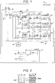
- FIG. 1 illustrates a block diagram of a stereo camera device 10.
- the stereo camera device 10 has two cameras of a left camera 21 and a right camera 22 as a photographing unit 20.
- the photographing unit 20 performs luminance correction or noise removal for images photographed by the left camera 21 and the right camera 22, and then writes the images to regions of a source image right 220 and a source image left 210 in an image memory 50 via a memory bus 70.
- the source image right 220 and the source image left 210 written in this way are transmitted to an internal bus 80 by a memory access management 40.
- the image memory 50 (a first memory) is connected to the memory bus 70 (a first bus) to store the source image right 220 and the source image left 210 (image data) .
- the memory access management 40 (memory access management unit) is connected to the memory bus 70 and the internal bus 80 (a second bus) for reading the source image right 220 and the source image left 210 from the image memory 50, respectively, via the memory bus 70 and outputting the read source image right 220 and source image left 210 to the internal bus 80.
- the memory access management 40 reads the image data from the image memory 50 instead of a processing unit A 30, a processing unit B 31, and a processing unit C 32 (a plurality of processing units), a traffic of the memory bus 70 is suppressed when there are the plurality of processing units that perform processing on the image data of any region.
- the memory access management 40 outputs the image data to the internal bus 80, the plurality of processing units can appropriately perform parallel processing. Accordingly, the image data can be processed at a high speed.
- the memory access management 40 detects the amount of the image written to the image memory 50 by the photographing unit 20 by a control signal 103 and controls an access timing of the image memory 50. In addition, the memory access management 40 detects an execution state of each processing unit by control signals 100, 101, and 102, and determines whether each processing unit is ready to receive the image data.
- processing management A 300, B 310, and C 320 as the processing management units detect the execution state of the processing of the processing unit A 30, the processing unit B 31, and the processing unit C 32, respectively.
- the memory access management 40 (memory access management unit) acquires the execution state of the processing of the processing unit A 30, the processing unit B 31, and the processing unit C 32 via the control signals 100, 101, and 102, and determines whether or not the processing unit A 30, the processing unit B 31, and the processing unit C 32 can receive the image data from the acquired execution state. Accordingly, when the processing unit of processing the image data can receive the image data, the memory access management 40 may distribute the image data.
- the processing unit A 30 receives data of the source image right 220 and the source image left 210 from the internal bus 80 and stores the data in a memory buffer A 301. After an affine transformation processing is performed on the stored image data in the affine transformation A 302 to perform distortion correction, a parallax of the left and right images is calculated in a parallax calculation A 303 to calculate parallax data. The calculated parallax data is written in a region of a parallax image 502 of the image memory 50.
- the memory buffer A 301 stores the image data output to the internal bus 80 (the second bus).
- the affine transformation A 302 affine transformation unit
- the parallax calculation A 303 calculates the parallax from the image data which is affine-transformed by the affine transformation A 302.
- the processing management A 300 performs a control for collect the image data of the internal bus 80 in the memory buffer A 301.
- the processing unit B 31 and the processing unit C 32 have the same function as the processing unit A 30, and these processing units perform a parallel processing, thereby realizing high-speed image processing.
- processing unit A 30, the processing unit B 31, and the processing unit C 32 are connected to the internal bus 80 (the second bus) to process the image data output to the internal bus 80.
- a CPU 60 performs processing such as detection of an obstacle by using the parallax image 502 while controlling the stereo camera device 10.
- the CPU 60, the photographing unit 20, the memory access management 40, the processing unit A 30, the processing unit B 31, the processing unit C 31, and the internal bus 80 are mounted on the same system on a chip (SoC) 90.
- SoC system on a chip
- FIG. 2 illustrates an outline of processing of the affine transformation A 302.
- the images photographed by the left camera 21 and the right camera 22 are distorted by a lens and are written in the source image right 220 and the source image left 210 with the distortion.
- An image of the source image right 220 in FIG. 2 illustrates an example of distortion when a rectangular pattern is photographed.
- the image is affine-transformed by the affine transformation A 302
- the image is transformed into a correct rectangular pattern like an image of a right after affine transformation 2209. This processing is similarly performed for the source image left 210.
- an affine transformation B 312 and an affine transformation C 322 have the same function.
- FIG. 3 illustrates an example of a memory access when the affine transformation A 302 performs transformation processing.
- a curve 2204 in the source image right 220 is transformed into a straight line 2206 of the right after affine transformation 2209
- image data of a region of an A block line 2201 is read, and affine transformation processing of the entire region is performed.
- a curve 2205 is transformed into a straight line 2207
- a region of a B block line 2202 is read and processing is performed.
- the A block line 2201 and the B block line 2202 have overlapping regions indicated by an overlapped line 2203.
- processing unit A 30 and the processing unit B 31 process image data of different regions. Each region has a portion overlapping another region.
- the processing unit A 30 processes the A block line 2201 and the processing unit B 31 processes the B block line 2202 in a shared manner
- the image data of the overlapped line 2203 are read by both the processing unit A 30 and the processing unit B 31. Therefore, when the processing unit A 30 and the processing unit B 31 independently access the image memory 50, the bus traffic of the memory bus 70 is increased by the overlapped line 2203.
- the memory access management 40 accesses the image memory 50 instead of each processing unit and distributes the accessed data to each processing unit, thereby preventing the traffic of the memory bus 70 from being increased.
- FIG. 4 illustrates parallax calculation processing of the parallax calculation A 303.
- the image photographed by the right camera 22 is used as a criteria image, and a criteria block image 221 such as 8 pixels ⁇ 8 pixels, for example, is defined.
- a size of the block image is not limited to this example.
- a reference image with a search width for example, 128 pixels
- SAD a difference between the criteria block image 221 and the reference image. This difference calculation is called SAD and performs the following calculation.
- FIG. 4 In an actual scenery 230 seen from a front window of the vehicle illustrated in FIG. 4 , there is a front vehicle 200.
- a part 201 of the front vehicle 200 is photographed at a position of the criteria block image 221 in the source image right 220 and is photographed at a position of the reference block image 211 in the source image left 210.
- a parallax d occurs in the position of the criteria block image 221 and the reference block image 211.
- This parallax d becomes a large value when the front vehicle 200 is close to the stereo camera device 10, and becomes a small value when the front vehicle 200 is far from the stereo camera device 10.
- the parallax obtained in this way is obtained in the whole image.
- a distance from the front vehicle 200 (a subject) to the stereo camera device 10 can be measured by a principle of triangulation.
- the distance Z from the parallax d is obtained by the following equation.
- xr is an x coordinate on the source image right 220
- yr is a y coordinate on the source image right 220.
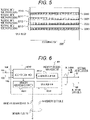
- FIG. 5 describes a source image of the image memory 50 and a sharing of each processing unit.
- the source image right 220 is divided in a horizontal direction in a block line unit.
- the processing unit A 30 performs processing of a block line 2210
- the processing unit B 31 performs processing of a block line 2211
- the processing unit C 32 performs processing of a block line 2212.
- the processing unit A 30 takes charge of the block line 2213, and the processing is sequentially performed from the processing unit A 30 to the processing unit C 32 for each block line.
- an overlapped line 2220 is a region necessary for both the processing unit A 30 and the processing unit B 31, and an overlapped region 2221 is a region necessary for both the processing unit B 31 and the processing unit C 32.
- the source image left 210 is also divided in the same way.
- FIG. 6 illustrates a configuration of a memory access management A 40.
- the memory bus 70 used when the memory access management A 40 reads the image data from the image memory 50 is constituted by a memory address bus 71 and a memory data bus 72.
- An access control 4010 detects that an image of one raster (one line) or more is written in the source image right 220 and the source image left 210 of the image memory 50 by the control signal 103, and outputs an address of the source image right 220 of the image memory 50 to the memory address bus 71, and the image memory 50 outputs data indicated by the address to the memory data bus 72.
- the output data is collected (stored) in a data buffer 4013.
- each processing unit can receive data by the control signals 100, 101, and 102, and an address of the data read from the image memory 50 is input to the address buffer 4012 and is output to the internal address bus 81 of the internal bus 80.
- data of a data buffer 4013 is output to an internal data bus 82.
- the memory access management A 40 (memory access management unit) reads the image data line by line and outputs the read image data to the internal bus 80 (second bus) line by line. Accordingly, each of the plurality of processing units can appropriately receive the one line of image data output to the internal bus 80.
- FIG. 7 illustrates a configuration of the processing management A 300 of the processing unit A 30.
- the internal address bus 81 of the internal bus 80 is connected to a comparator 3002 and a comparator 3004.
- the comparator 3002 compares a magnitude relation with a start address 3001.
- the start address 3001 indicates a start address of a data region to be processed by the processing unit A 30, and the comparator 3002 determines that the internal address bus 81 indicates an address of the start address 3001 or more.
- An end address 3003 indicates an end address of a data region to be processed by the processing unit A 30, and the comparator 3004 determines that the internal address bus 81 indicates an address of the end address 3003 or less. These determination results are sent to an AND (logical AND) 3005, where data of the internal data bus 82 is collected in the internal data buffer 3006 only when both are established.
- the start address 3001 and the end address 3003 may have a plurality of sets.
- the processing management B 310 and the processing management C 320 also perform the same processing.
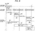
- FIG. 8 is a time chart illustrating an access of the image memory 50 and a timing of processing of each processing unit. Originally, both the source image right 220 and the source image left 210 are accessed, but here, the source image right 220 is described. First, the image photographed by the photographing unit 20 is written at a timing indicated by a source image writing line.
- Data 5001 is a first line 0 (the highest raster of the image) written by the photographing unit 20, data 5002 is a line 1, and continuous raster data is written in the same manner thereafter.
- the memory access management 40 reads a first line of the source image right 220 in data 5003, and then reads the data line by line in the order of the data 5004.
- the processing unit A 30 receives the data.
- the processing unit A 30 and the processing unit B 31 receive the data redundantly.
- a period 5007 the processing unit B 31 receives the data.
- the processing unit B 31 and the processing unit C 32 receive the data redundantly.
- a processing C 32 receives the data.
- a period 5010 indicates a period during which the data read by the memory access management 40 is collected in the memory buffer A 301 of the processing unit A 30. That is, the processing management A 300 of the processing unit A 30 collects data from a line 0 to a line 13 output to the internal data bus 82 in the memory buffer A 301.
- the processing unit A 30 (first processing unit) receives image data from the line 0 (a first line) to the line 13 (a second line). In addition, the processing unit A 30 corrects (affine-transforms) distortion of the received image data, as described with reference to FIG. 1 .
- a period 5011 indicates a period during which the data read by the memory access management 40 is collected in a memory buffer B 311 of the processing unit B 31. That is, the processing management B 310 of the processing unit B 31 collects data from a line 10 to a line 23 output to the internal data bus 82 in the memory buffer B 311.
- the processing unit B 31 receives image data from the line 10 (a third line) located between the line 0 (the first line) and the line 13 (the second line) to the line 23 (a fourth line) . Accordingly, the processing unit A 30 and the processing unit B 31 can perform parallel processing for the image data from the line 10 to the line 13. In addition, the processing unit B 31 corrects distortion of the received image data, as described with reference to FIG. 1 .
- a period 5012 indicates a period during which the data read by the memory access management 40 is collected in a memory buffer C 321 of the processing unit C 32. That is, the processing management C 320 of the processing unit C 32 collects data from a line 20 to a line 33 output to the internal data bus 82 in the memory buffer C 321.
- the data of the source image right 220 is accessed once from the line 0 to the end.
- the memory buffer A 301 and the memory buffer B 311 simultaneously collect the same data on the internal data bus 82 so that each processing unit (for example, the processing unit A and the processing unit B) can receive the data.
- the amount of data read from the image memory 50 (the first memory) by the memory access management 40 is smaller than a total sum of the amount of data processed by the plurality of processing units (the processing unit A 30, the processing unit B 31, and the processing unit C 32), respectively.
- the processing unit A 30 starts affine transformation processing at the time when data corresponding to one block line is collected in the memory buffer A 301. The same applies to the processing unit B 31 and the processing unit C 32.
- FIG. 13 illustrates an example of an operation of the memory buffer and a processing period of calculation processing. Since the processing time of the affine transformation processing and the parallax calculation processing, that is, the periods of 5013, 5014, and 5015 are sufficiently late than a time in which the memory access management 40 reads the image memory 50 line by line and the data is stored in the memory buffer, that is, a period of the sum of 5010, 5011, and 5012, there is a period 5016p in which the affine transformation and parallax calculation processing of the processing unit A 30 to the processing unit C 32 are processed in parallel. In addition, since a period 5016 in which the image photographed by the photographing unit 20 is written in the image memory 50, and a memory read of the memory access management 40 can also be processed in parallel, the system can be speeded up.
- FIG. 9 illustrates a processing flow of the memory access management 40. It is determined whether or not the photographing unit 20 writes one or more lines of data in the source image right 220 or the source image left 210 and waits for the processing until one or more lines of data have been written (S110). If one or more lines of data are written, the data is read from the source image right 220 (or the source image left 210) (S120).
- an address is updated for the next access (S130).
- the read data is output to the internal bus 80 (S140) .
- the processing is repeated until the last line of the source image right 220 (or the source image left 210) is read (S150).
- the memory access management 40 reads the source image right 220 (or the source image left 210) without repeating the access to the same line.
- the memory access management 40 detects that one or more lines of image data are written in the image memory 50 (the first memory) .
- the memory access management 40 reads the image data line by line from the image memory 50 via the memory bus 70 (the first bus) and outputs the read image data to the internal bus 80 (the second bus).
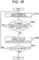
- FIG. 10 illustrates an operation flow of the processing management A 300.
- An address sent from the memory access management 40 to the internal address bus 81 is acquired (S210) . It is determined whether the acquired address is the start address 3001 or more and is the end address 3003 or less (S220) . If the condition is satisfied, the data is collected from the internal data bus 82 when the condition is satisfied and is stored in the memory buffer A 301. Thereafter, the processing is repeated until the defined processing ends (S240).
- This processing is performed for the processing management B 310 and the processing management C 320 in the same way, and it is independently determined whether or not the data is received from the internal bus 80 by an address comparison by the start address 3001 and the end address 3003 which are respectively set. Therefore, if the condition is simultaneously satisfied in the plurality of processing units, the data can be simultaneously collected.
- the memory access management 40 can prevent the overlapped access of the image memory 50 to the overlapped region commonly used by the plurality of processing units, an increase of the traffic of the memory bus 70 can be prevented.
- the image data can be processed at a high speed while suppressing the bus traffic.
- the memory access management 40 has a local memory 4015 (second memory)
- the local memory 4015 has a capacity equal to or greater than the overlapped line 2203 illustrated in FIG. 3 . Accordingly, a timing of data distribution to each processing unit can be adjusted.
- Each processing unit writes the parallax image of the parallax calculation result in the image memory 50 via the memory bus 70. For this reason, there is a possibility that the writing of the parallax image may be waited depending on an operation state of the memory bus 70. Therefore, an operable timing of each processing unit is deviated.
- FIG. 8 although the plurality of processing units simultaneously receive the data from the memory access management 40, there is a possibility that the simultaneous reception becomes impossible due to a deviation of the operation timing of each processing unit. Therefore, the overlapped line is stored in the local memory 4015, and the data is transmitted individually to each processing unit.
- FIG. 12 illustrates an operation time chart of the second embodiment.
- a difference from FIG. 8 is that there is a retransmission period 5013.
- the memory access management 40 temporarily idles the access of the source image right 220. This assumes a case in which the operation of the processing unit B 31 becomes a little slower than that in FIG. 8 , and the processing unit B 31 cannot receive the overlapped portion with the processing unit A 30 at the same time.
- the memory access management 40 transmits the data of the line 10 again to the internal bus 80 (local bus) in the retransmission period 5013 and sends it to the processing unit B 31.
- the memory access management 40 (memory access management unit) stores the image data from the line 10 (the third line) to the line 13 (the second line) in the local memory 4015 (the second memory) and stops reading of the image data after a line 14 next to the line 13. Subsequently, when the processing unit B 31 may receive the image data, the memory access management 40 outputs the image data from the line 10 to the line 13 stored in the local memory 4015 to the internal bus 80 (the second bus) .
- the local memory 4015 even if the operation timing of each processing unit is deviated, the overlapped access of the image memory 50 can be prevented.
- the present invention is not limited to the embodiments described above, but includes various variations.
- the embodiments described above have been described in detail in order to explain the present invention in detail, and are not necessarily limited to those having all the configurations described above.
- the photographing unit 20 (a capturing unit) is constituted by the two cameras, but the number of cameras constituting the photographing unit 20 is arbitrary.
- the photographing unit 20 is constituted by a single camera, the parallax calculation is not possible, but the affine transformation processing can be performed at a high speed by applying the present invention to correct the distortion of the image data.
- the memory access management 40 may read image data of an image data region according to priority corresponding to the image data region, and may output the read image data of the region to the internal bus 80 (the second bus). Accordingly, the image data of a region having high priority is first distributed and is processed by a processing unit responsible for the region.
- the region and priority of the image data are stored corresponding to a predetermined memory (storage device), for example, as illustrated in FIG. 14 .
- embodiments of the present invention may have the following aspects.
- the memory access management unit representatively reads the image data commonly used by the plurality of processing units from the image memory. Since the common image data is distributed to each processing unit as needed by the memory access management unit, an increase in bus traffic of the image memory can be suppressed even if the processing unit is increased. For this reason, it is possible to perform high-speed processing in accordance with the degree of parallelism of the processing unit.
Landscapes
- Engineering & Computer Science (AREA)
- Theoretical Computer Science (AREA)
- Physics & Mathematics (AREA)
- General Physics & Mathematics (AREA)
- Signal Processing (AREA)
- Multimedia (AREA)
- General Engineering & Computer Science (AREA)
- Computer Vision & Pattern Recognition (AREA)
- Mathematical Physics (AREA)
- Image Processing (AREA)
- Traffic Control Systems (AREA)
- Image Analysis (AREA)
- Measurement Of Optical Distance (AREA)
- Memory System (AREA)
- Studio Devices (AREA)
Description
- The present invention relates to a camera device.
- In order to improve running safety of a vehicle, a system for detecting an obstacle in front of the vehicle by a camera mounted on the vehicle and giving a driver an alarm or performing an automatic brake when there is a possibility that the vehicle may collide with the obstacle has been studied.
- Sensors for monitoring the front of the vehicle include millimeter-wave radar, laser radar, a camera, and the like. As a type of the camera, there are a monocular camera and a stereo camera using a plurality of cameras. The stereo camera can measure a distance to a photographed object by using a parallax of an overlapping region photographed with two cameras at a predetermined interval. Therefore, the stereo camera can accurately detect the risk of collision to the front object.
- The stereo camera obtains a parallax of images photographed by two cameras, and converts the parallax into a distance. In order to obtain the parallax, it is necessary to perform matching determination of images between the two cameras. Since the matching process has a large amount of calculation, a method of processing by hardware has been devised. However, in the future, it is expected that the number of photographed pixels of the camera is increased and a frame rate is further increased, and additional high-speed processing of the parallax calculation is required.
- Therefore, there has been proposed a method of realizing the high-speed processing by performing geometric correction processing, texture detection processing, parallax calculation processing, and the like for each small region in parallel (for example, see PTL 1).
- In addition, there has been proposed a method of performing parallel image processing for each region of an image memory having a plurality of processing modules and divided into a plurality of regions (for example, see PTL 2).
-
- PTL 1:
JP 2012-18014 A - PTL 2:
JP 2007-72867 A - In
PTL 1, the calculations necessary for calculating the parallax of the stereo camera are divided into detailed steps, and these calculations are pipelined to realize high-speed processing. According to the method, the calculations to be processed in parallel are speeded up, and the amount of image data required for the calculations is also increased. Therefore, if the number of pipeline processing stages is increased for additional high-speed processing, there is a problem that a bus traffic of a memory is increased, which hinders the improvement of the processing speed. - In
PTL 2, a plurality of function modules having the same calculation function are prepared and are operated in parallel to realize high-speed processing. According to the method, it is possible to speed up the calculation according to the number of functional modules. However, there is a problem that as the number of functional modules increases, the bus traffic in a main memory increases, which hinders high-speed processing. -
US 2006/114330 A1 discloses an electronic camera with the features in the preamble ofpresent claim 1. Other conventional camera devices are described inUS 2011/242342 A1 andUS 2011/141308 A1 .US 5.483.642B discloses an architecture for parallel processing of data where also two busses are used and access of the processing units to the bus connected to the main memory is only possible through a memory access management unit. - An object of the present invention is to provide a camera device capable of processing image data at a high speed while suppressing a bus traffic.
- In order to achieve the object, a camera device according to the present invention includes the features defined in appended
claim 1. The dependent claims relate to preferred embodiments. - According to the present invention, the image data can be processed at a high speed while suppressing the bus traffic. Other problems, structures, and effects are apparent from the description of the embodiments below.
-
- [
FIG. 1] FIG. 1 is a functional block diagram of a stereo camera device. - [
FIG. 2] FIG. 2 is an explanation diagram of an affine transformation processing. - [
FIG. 3] FIG. 3 is a diagram illustrating duplicate accesses of an image memory by the affine transformation processing. - [
FIG. 4] FIG. 4 is an explanation diagram of a parallax calculation. - [
FIG. 5] FIG. 5 is a diagram for describing a classification of the image memory and a division of a processing unit. - [
FIG. 6] FIG. 6 is a block diagram of a memory access management. - [
FIG. 7] FIG. 7 is a block diagram of a processing management. - [
FIG. 8] FIG. 8 is a diagram illustrating an example of a time chart of access of the image memory and data distribution to the processing unit. - [
FIG. 9] FIG. 9 is a processing flow of a memory access management. - [
FIG. 10] FIG. 10 is a block diagram of a processing management. - [
FIG. 11] FIG. 11 is a block diagram of a second embodiment in which a local memory is installed on the memory access management. - [
FIG. 12] FIG. 12 is a diagram illustrating an example of an operation time chart ofFIG. 11 . - [
FIG. 13] FIG. 13 is a diagram illustrating an example of an operation of a memory buffer and a processing period of calculation processing. - [
FIG. 14] FIG. 14 is a diagram illustrating a correspondence relationship between a region of image data and priority. - A configuration and an operation of a stereo camera device (camera device) according to first and second embodiments of the present invention are hereinafter described with reference to the drawings. The stereo camera device is, for example, an on-board stereo camera device used for recognition of an obstacle outside a vehicle. In addition, in the drawings, the same reference numerals denote the same parts.
-
FIG. 1 illustrates a block diagram of astereo camera device 10. Thestereo camera device 10 has two cameras of aleft camera 21 and aright camera 22 as a photographingunit 20. The photographingunit 20 performs luminance correction or noise removal for images photographed by theleft camera 21 and theright camera 22, and then writes the images to regions of a source image right 220 and a source image left 210 in animage memory 50 via amemory bus 70. The source image right 220 and the source image left 210 written in this way are transmitted to aninternal bus 80 by amemory access management 40. - In other words, the image memory 50 (a first memory) is connected to the memory bus 70 (a first bus) to store the source image right 220 and the source image left 210 (image data) . The memory access management 40 (memory access management unit) is connected to the
memory bus 70 and the internal bus 80 (a second bus) for reading thesource image right 220 and the source image left 210 from theimage memory 50, respectively, via thememory bus 70 and outputting the readsource image right 220 and source image left 210 to theinternal bus 80. - Since the
memory access management 40 reads the image data from theimage memory 50 instead of aprocessing unit A 30, aprocessing unit B 31, and a processing unit C 32 (a plurality of processing units), a traffic of thememory bus 70 is suppressed when there are the plurality of processing units that perform processing on the image data of any region. In addition, since thememory access management 40 outputs the image data to theinternal bus 80, the plurality of processing units can appropriately perform parallel processing. Accordingly, the image data can be processed at a high speed. - The
memory access management 40 detects the amount of the image written to theimage memory 50 by the photographingunit 20 by acontrol signal 103 and controls an access timing of theimage memory 50. In addition, thememory access management 40 detects an execution state of each processing unit bycontrol signals - In other words, processing
management A 300,B 310, andC 320 as the processing management units detect the execution state of the processing of theprocessing unit A 30, theprocessing unit B 31, and theprocessing unit C 32, respectively. The memory access management 40 (memory access management unit) acquires the execution state of the processing of theprocessing unit A 30, theprocessing unit B 31, and theprocessing unit C 32 via the control signals 100, 101, and 102, and determines whether or not theprocessing unit A 30, theprocessing unit B 31, and theprocessing unit C 32 can receive the image data from the acquired execution state. Accordingly, when the processing unit of processing the image data can receive the image data, thememory access management 40 may distribute the image data. - The
processing unit A 30 receives data of the source image right 220 and the source image left 210 from theinternal bus 80 and stores the data in amemory buffer A 301. After an affine transformation processing is performed on the stored image data in theaffine transformation A 302 to perform distortion correction, a parallax of the left and right images is calculated in aparallax calculation A 303 to calculate parallax data. The calculated parallax data is written in a region of aparallax image 502 of theimage memory 50. - In other words, the
memory buffer A 301 stores the image data output to the internal bus 80 (the second bus). The affine transformation A 302 (affine transformation unit) affine-transforms the image data stored in thememory buffer A 301. The parallax calculation A 303 (parallax calculation unit) calculates the parallax from the image data which is affine-transformed by theaffine transformation A 302. - The
processing management A 300 performs a control for collect the image data of theinternal bus 80 in thememory buffer A 301. Theprocessing unit B 31 and theprocessing unit C 32 have the same function as theprocessing unit A 30, and these processing units perform a parallel processing, thereby realizing high-speed image processing. - In other words, the
processing unit A 30, theprocessing unit B 31, and the processing unit C 32 (a plurality of processing units) are connected to the internal bus 80 (the second bus) to process the image data output to theinternal bus 80. - In addition, a
CPU 60 performs processing such as detection of an obstacle by using theparallax image 502 while controlling thestereo camera device 10. - In addition, in the
stereo camera device 10, it is assumed that theCPU 60, the photographingunit 20, thememory access management 40, theprocessing unit A 30, theprocessing unit B 31, theprocessing unit C 31, and theinternal bus 80 are mounted on the same system on a chip (SoC) 90. Each processing unit of theSoC 90 accesses the image memory via thememory bus 70. Therefore, in order to speed-up the system, it is necessary to reduce bus traffic of thememory bus 70. -
FIG. 2 illustrates an outline of processing of theaffine transformation A 302. The images photographed by theleft camera 21 and theright camera 22 are distorted by a lens and are written in the source image right 220 and the source image left 210 with the distortion. An image of the source image right 220 inFIG. 2 illustrates an example of distortion when a rectangular pattern is photographed. When the image is affine-transformed by theaffine transformation A 302, the image is transformed into a correct rectangular pattern like an image of a right afteraffine transformation 2209. This processing is similarly performed for the source image left 210. In addition, anaffine transformation B 312 and anaffine transformation C 322 have the same function. -
FIG. 3 illustrates an example of a memory access when theaffine transformation A 302 performs transformation processing. In an example in which acurve 2204 in the source image right 220 is transformed into astraight line 2206 of the right afteraffine transformation 2209, image data of a region of anA block line 2201 is read, and affine transformation processing of the entire region is performed. In addition, when acurve 2205 is transformed into astraight line 2207, a region of aB block line 2202 is read and processing is performed. In this case, theA block line 2201 and theB block line 2202 have overlapping regions indicated by an overlappedline 2203. - In other words, the
processing unit A 30 and the processing unit B 31 (a plurality of processing units) process image data of different regions. Each region has a portion overlapping another region. - For example, when the
processing unit A 30 processes theA block line 2201 and theprocessing unit B 31 processes theB block line 2202 in a shared manner, the image data of the overlappedline 2203 are read by both theprocessing unit A 30 and theprocessing unit B 31. Therefore, when theprocessing unit A 30 and theprocessing unit B 31 independently access theimage memory 50, the bus traffic of thememory bus 70 is increased by the overlappedline 2203. - Therefore, in the present embodiment, the
memory access management 40 accesses theimage memory 50 instead of each processing unit and distributes the accessed data to each processing unit, thereby preventing the traffic of thememory bus 70 from being increased. -
FIG. 4 illustrates parallax calculation processing of theparallax calculation A 303. The image photographed by theright camera 22 is used as a criteria image, and acriteria block image 221 such as 8 pixels × 8 pixels, for example, is defined. A size of the block image is not limited to this example. On the other hand, in the image photographed by theleft camera 21, a reference image with a search width (for example, 128 pixels) is selected based on the same vertical position (Y coordinate) and horizontal position (X coordinate) as the criteria blockimage 221. Thereafter, a difference between the criteria blockimage 221 and the reference image is calculated. This difference calculation is called SAD and performs the following calculation. - [Equation 1]

where I is an 8 × 8 image block in the reference image, T is image data of the criteria blockimage 221, and i and j are coordinates in the image block. In order to calculate one parallax, a reference position of the reference image is shifted one by one and a calculation is performed by the search width to search for a position where an SAD value becomes the smallest. - In an
actual scenery 230 seen from a front window of the vehicle illustrated inFIG. 4 , there is afront vehicle 200. When there are the source image right 220 photographed by theright camera 22 and the source image left 210 photographed by theleft camera 21, apart 201 of thefront vehicle 200 is photographed at a position of the criteria blockimage 221 in the source image right 220 and is photographed at a position of thereference block image 211 in the source image left 210. - As a result, a parallax d occurs in the position of the criteria block
image 221 and thereference block image 211. This parallax d becomes a large value when thefront vehicle 200 is close to thestereo camera device 10, and becomes a small value when thefront vehicle 200 is far from thestereo camera device 10. The parallax obtained in this way is obtained in the whole image. By using the parallax d, a distance from the front vehicle 200 (a subject) to thestereo camera device 10 can be measured by a principle of triangulation. The distance Z from the parallax d is obtained by the following equation. - [Equation 2]

where f is a focal distance of the right and left cameras, and B is a distance between theright camera 22 and the left camera 21 (baseline length) . In addition, in order to transform the parallax data into three dimensions, distances in the X and Y directions on the three dimensions of the point where Z is obtained are expressed by the following equations. - [Equation 3]

- [Equation 4]

where xr is an x coordinate on the source image right 220 and yr is a y coordinate on the source image right 220. As described above, the position (X, Y, Z) on a three-dimensional space of the subject can be obtained as the distance Z from thestereo camera device 10 by the images photographed by thestereo camera device 10. -
FIG. 5 describes a source image of theimage memory 50 and a sharing of each processing unit. The source image right 220 is divided in a horizontal direction in a block line unit. Theprocessing unit A 30 performs processing of ablock line 2210, theprocessing unit B 31 performs processing of ablock line 2211, and theprocessing unit C 32 performs processing of ablock line 2212. Theprocessing unit A 30 takes charge of theblock line 2213, and the processing is sequentially performed from theprocessing unit A 30 to theprocessing unit C 32 for each block line. In addition, an overlappedline 2220 is a region necessary for both theprocessing unit A 30 and theprocessing unit B 31, and an overlappedregion 2221 is a region necessary for both theprocessing unit B 31 and theprocessing unit C 32. The source image left 210 is also divided in the same way. -
FIG. 6 illustrates a configuration of a memoryaccess management A 40. Thememory bus 70 used when the memoryaccess management A 40 reads the image data from theimage memory 50 is constituted by a memory address bus 71 and a memory data bus 72. Anaccess control 4010 detects that an image of one raster (one line) or more is written in the source image right 220 and the source image left 210 of theimage memory 50 by thecontrol signal 103, and outputs an address of the source image right 220 of theimage memory 50 to the memory address bus 71, and theimage memory 50 outputs data indicated by the address to the memory data bus 72. The output data is collected (stored) in adata buffer 4013. - Thereafter, it is confirmed that each processing unit can receive data by the control signals 100, 101, and 102, and an address of the data read from the
image memory 50 is input to theaddress buffer 4012 and is output to theinternal address bus 81 of theinternal bus 80. In addition, data of adata buffer 4013 is output to aninternal data bus 82. When the access to data by one raster of the source image right 220 is terminated, an access to data by one raster of the source image left 210 is performed. Thereafter, the source image right 220 and the source image left 210 are alternately accessed. - In other words, the memory access management A 40 (memory access management unit) reads the image data line by line and outputs the read image data to the internal bus 80 (second bus) line by line. Accordingly, each of the plurality of processing units can appropriately receive the one line of image data output to the
internal bus 80. -
FIG. 7 illustrates a configuration of theprocessing management A 300 of theprocessing unit A 30. Theinternal address bus 81 of theinternal bus 80 is connected to acomparator 3002 and acomparator 3004. Thecomparator 3002 compares a magnitude relation with astart address 3001. Thestart address 3001 indicates a start address of a data region to be processed by theprocessing unit A 30, and thecomparator 3002 determines that theinternal address bus 81 indicates an address of thestart address 3001 or more. - An
end address 3003 indicates an end address of a data region to be processed by theprocessing unit A 30, and thecomparator 3004 determines that theinternal address bus 81 indicates an address of theend address 3003 or less. These determination results are sent to an AND (logical AND) 3005, where data of theinternal data bus 82 is collected in theinternal data buffer 3006 only when both are established. Thestart address 3001 and theend address 3003 may have a plurality of sets. Theprocessing management B 310 and theprocessing management C 320 also perform the same processing. -
FIG. 8 is a time chart illustrating an access of theimage memory 50 and a timing of processing of each processing unit. Originally, both the source image right 220 and the source image left 210 are accessed, but here, the source image right 220 is described. First, the image photographed by the photographingunit 20 is written at a timing indicated by a source image writing line. -
Data 5001 is a first line 0 (the highest raster of the image) written by the photographingunit 20,data 5002 is aline 1, and continuous raster data is written in the same manner thereafter. On the other hand, thememory access management 40 reads a first line of the source image right 220 indata 5003, and then reads the data line by line in the order of thedata 5004. In aperiod 5005, theprocessing unit A 30 receives the data. In aperiod 5006, theprocessing unit A 30 and theprocessing unit B 31 receive the data redundantly. - In a
period 5007, theprocessing unit B 31 receives the data. In aperiod 5008, theprocessing unit B 31 and theprocessing unit C 32 receive the data redundantly. In aperiod 5009, aprocessing C 32 receives the data. Aperiod 5010 indicates a period during which the data read by thememory access management 40 is collected in thememory buffer A 301 of theprocessing unit A 30. That is, theprocessing management A 300 of theprocessing unit A 30 collects data from aline 0 to aline 13 output to theinternal data bus 82 in thememory buffer A 301. - In other words, the processing unit A 30 (first processing unit) receives image data from the line 0 (a first line) to the line 13 (a second line). In addition, the
processing unit A 30 corrects (affine-transforms) distortion of the received image data, as described with reference toFIG. 1 . - A
period 5011 indicates a period during which the data read by thememory access management 40 is collected in amemory buffer B 311 of theprocessing unit B 31. That is, theprocessing management B 310 of theprocessing unit B 31 collects data from aline 10 to aline 23 output to theinternal data bus 82 in thememory buffer B 311. - In other words, the processing unit B 31 (a second processing unit) receives image data from the line 10 (a third line) located between the line 0 (the first line) and the line 13 (the second line) to the line 23 (a fourth line) . Accordingly, the
processing unit A 30 and theprocessing unit B 31 can perform parallel processing for the image data from theline 10 to theline 13. In addition, theprocessing unit B 31 corrects distortion of the received image data, as described with reference toFIG. 1 . - A
period 5012 indicates a period during which the data read by thememory access management 40 is collected in amemory buffer C 321 of theprocessing unit C 32. That is, theprocessing management C 320 of theprocessing unit C 32 collects data from aline 20 to a line 33 output to theinternal data bus 82 in thememory buffer C 321. - In this drawing, the data of the source image right 220 is accessed once from the
line 0 to the end. However, for example, in the overlapped period such as theperiod 5006, thememory buffer A 301 and thememory buffer B 311 simultaneously collect the same data on theinternal data bus 82 so that each processing unit (for example, the processing unit A and the processing unit B) can receive the data. - In other words, the amount of data read from the image memory 50 (the first memory) by the memory access management 40 (the memory access management unit) is smaller than a total sum of the amount of data processed by the plurality of processing units (the
processing unit A 30, theprocessing unit B 31, and the processing unit C 32), respectively. - Therefore, overlapped access to data is removed to prevent an increase of the bus traffic.
- The
processing unit A 30 starts affine transformation processing at the time when data corresponding to one block line is collected in thememory buffer A 301. The same applies to theprocessing unit B 31 and theprocessing unit C 32. -
FIG. 13 illustrates an example of an operation of the memory buffer and a processing period of calculation processing. Since the processing time of the affine transformation processing and the parallax calculation processing, that is, the periods of 5013, 5014, and 5015 are sufficiently late than a time in which thememory access management 40 reads theimage memory 50 line by line and the data is stored in the memory buffer, that is, a period of the sum of 5010, 5011, and 5012, there is aperiod 5016p in which the affine transformation and parallax calculation processing of theprocessing unit A 30 to theprocessing unit C 32 are processed in parallel. In addition, since aperiod 5016 in which the image photographed by the photographingunit 20 is written in theimage memory 50, and a memory read of thememory access management 40 can also be processed in parallel, the system can be speeded up. -
FIG. 9 illustrates a processing flow of thememory access management 40. It is determined whether or not the photographingunit 20 writes one or more lines of data in the source image right 220 or the source image left 210 and waits for the processing until one or more lines of data have been written (S110). If one or more lines of data are written, the data is read from the source image right 220 (or the source image left 210) (S120). - If one line of access is completed, an address is updated for the next access (S130). The read data is output to the internal bus 80 (S140) . The processing is repeated until the last line of the source image right 220 (or the source image left 210) is read (S150). As described above, the
memory access management 40 reads the source image right 220 (or the source image left 210) without repeating the access to the same line. - In other words, the memory access management 40 (the memory access management unit) detects that one or more lines of image data are written in the image memory 50 (the first memory) . When it is detected that one or more lines of image data are written in the
image memory 50, thememory access management 40 reads the image data line by line from theimage memory 50 via the memory bus 70 (the first bus) and outputs the read image data to the internal bus 80 (the second bus). -
FIG. 10 illustrates an operation flow of theprocessing management A 300. An address sent from thememory access management 40 to theinternal address bus 81 is acquired (S210) . It is determined whether the acquired address is thestart address 3001 or more and is theend address 3003 or less (S220) . If the condition is satisfied, the data is collected from theinternal data bus 82 when the condition is satisfied and is stored in thememory buffer A 301. Thereafter, the processing is repeated until the defined processing ends (S240). - This processing is performed for the
processing management B 310 and theprocessing management C 320 in the same way, and it is independently determined whether or not the data is received from theinternal bus 80 by an address comparison by thestart address 3001 and theend address 3003 which are respectively set. Therefore, if the condition is simultaneously satisfied in the plurality of processing units, the data can be simultaneously collected. - According to the first embodiment described above, since the
memory access management 40 can prevent the overlapped access of theimage memory 50 to the overlapped region commonly used by the plurality of processing units, an increase of the traffic of thememory bus 70 can be prevented. - That is, the image data can be processed at a high speed while suppressing the bus traffic.
- Next, an operation when the
memory access management 40 has a local memory 4015 (second memory) will be described as a second embodiment with reference toFIG. 11 . It is assumed that thelocal memory 4015 has a capacity equal to or greater than the overlappedline 2203 illustrated inFIG. 3 . Accordingly, a timing of data distribution to each processing unit can be adjusted. - Each processing unit writes the parallax image of the parallax calculation result in the
image memory 50 via thememory bus 70. For this reason, there is a possibility that the writing of the parallax image may be waited depending on an operation state of thememory bus 70. Therefore, an operable timing of each processing unit is deviated. InFIG. 8 , although the plurality of processing units simultaneously receive the data from thememory access management 40, there is a possibility that the simultaneous reception becomes impossible due to a deviation of the operation timing of each processing unit. Therefore, the overlapped line is stored in thelocal memory 4015, and the data is transmitted individually to each processing unit. -
FIG. 12 illustrates an operation time chart of the second embodiment. A difference fromFIG. 8 is that there is aretransmission period 5013. In theperiod 5010, after theline 0 to line 13 of thedata 5003 are transmitted to thememory buffer A 301, thememory access management 40 temporarily idles the access of the source image right 220. This assumes a case in which the operation of theprocessing unit B 31 becomes a little slower than that inFIG. 8 , and theprocessing unit B 31 cannot receive the overlapped portion with theprocessing unit A 30 at the same time. Thememory access management 40 transmits the data of theline 10 again to the internal bus 80 (local bus) in theretransmission period 5013 and sends it to theprocessing unit B 31. - In other words, when the processing unit A 30 (first processing unit) can receive the image data and the processing unit B 31 (second processing unit) cannot receive the image data, the memory access management 40 (memory access management unit) stores the image data from the line 10 (the third line) to the line 13 (the second line) in the local memory 4015 (the second memory) and stops reading of the image data after a
line 14 next to theline 13. Subsequently, when theprocessing unit B 31 may receive the image data, thememory access management 40 outputs the image data from theline 10 to theline 13 stored in thelocal memory 4015 to the internal bus 80 (the second bus) . - According to the second embodiment described above, by having the
local memory 4015, even if the operation timing of each processing unit is deviated, the overlapped access of theimage memory 50 can be prevented. - Note that the present invention is not limited to the embodiments described above, but includes various variations. For example, the embodiments described above have been described in detail in order to explain the present invention in detail, and are not necessarily limited to those having all the configurations described above. In addition, it is possible to replace some of the configurations of any embodiment with those of other embodiments, and it is also possible to add the constitution of another embodiment to the constitution of any embodiment. In addition, it is possible to add, delete, and replace other configurations for some of the configurations of each embodiment.
- In the above embodiment, the photographing unit 20 (a capturing unit) is constituted by the two cameras, but the number of cameras constituting the photographing
unit 20 is arbitrary. When the photographingunit 20 is constituted by a single camera, the parallax calculation is not possible, but the affine transformation processing can be performed at a high speed by applying the present invention to correct the distortion of the image data. - The memory access management 40 (memory access management unit) may read image data of an image data region according to priority corresponding to the image data region, and may output the read image data of the region to the internal bus 80 (the second bus). Accordingly, the image data of a region having high priority is first distributed and is processed by a processing unit responsible for the region. The region and priority of the image data are stored corresponding to a predetermined memory (storage device), for example, as illustrated in
FIG. 14 . - In addition, the embodiments of the present invention may have the following aspects.
- (1) A camera device including: an image memory storing image data; a plurality of processing units disposed in parallel to the image memory to process the image data; and a memory access management unit reading the image data from the image memory and distributing the image data to the plurality of processing units.
- (2) The camera device according to (1), wherein the memory access management unit simultaneously distributes the image data.
- (3) The camera device according to (1), wherein the processing region of each processing unit is set to be partially overlapped with the processing region of another processing unit.
- (4) The camera device according to (1), wherein the amount of data read from the image memory by the memory access management unit is smaller than the total sum of the amount of data necessary for the plurality of processing units.
- According to the above embodiments (1) to (4), the memory access management unit representatively reads the image data commonly used by the plurality of processing units from the image memory. Since the common image data is distributed to each processing unit as needed by the memory access management unit, an increase in bus traffic of the image memory can be suppressed even if the processing unit is increased. For this reason, it is possible to perform high-speed processing in accordance with the degree of parallelism of the processing unit.
-
- 10
- stereo camera device
- 20
- photographing unit
- 21
- left camera
- 22
- right camera
- 30
- processing unit A
- 31
- processing unit B
- 32
- processing unit C
- 40
- memory access management
- 50
- image memory
- 60
- CPU
- 70
- memory bus
- 80
- internal bus
- 90
- SoC
- 210
- source image left
- 220
- source image right
- 300
- processing management A
- 301
- memory buffer A
- 302
- affine transformation A
- 303
- parallax calculation A
- 310
- processing management B
- 311
- memory buffer B
- 312
- affine transformation B
- 313
- parallax calculation B
- 320
- processing management C
- 321
- memory buffer C
- 322
- affine transformation C
- 323
- parallax calculation C
- 4015
- local memory
Claims (8)
- A camera device (10) comprising:a photographing unit (20);a first bus (70);a first memory (50) connected to the first bus (70) to store image data written to the first memory (50) by the photographing unit (20);a second bus (80);a memory access management unit (40) connected to the first bus (70) and the second bus (80) to read the image data from the first memory (50) via the first bus (70) and to output the read image data to the second bus (80); anda plurality of processing units (30-32) connected to the second bus (80) to process the image data output to the second bus (80),characterised in thatthe plurality of processing units (30-32) have the same function and are adapted to perform parallel processing of different regions (2210-2213) of the image data output to the second bus (80), each region having a portion (2220-2223) overlapping another region, andthe memory access management unit (40) is adapted to access the image memory (50) instead of the processing units (30-32) and to distribute the accessed data to each processing unit (30-32), thereby preventing the traffic of the first bus (70) from being increased by overlapped access to the image memory (50) for the overlapped regions (2220-2223) commonly used by the plurality of processing units (30-32).
- The camera device (10) according to claim 1, wherein the memory access management unit (40) is adapted to read the image data line by line, and output the read image data to the second bus (80) line by line.
- The camera device (10) according to claim 2, whereinthe plurality of processing units (30-32) include at least a first processing unit (30) and a second processing unit (31),the first processing unit (30) is adapted to receive the image data from a first line to a second line, and correct distortion of the received image data, andthe second processing unit (31) is adapted to receive the image data from a third line located between the first line and the second line to a fourth line, and correct distortion of the received image data.
- The camera device (10) according to claim 3, further comprising a second memory (4015),
wherein the memory access management unit (40) is adapted to store the image data from the third line to the second line in the second memory (4015) and stop reading of the image data after a line next to the second line when the first processing unit (30) receives the image data and the second processing unit (31) does not receive the image data, and output the image data from the third line to the second line stored in the second memory (4015) to the second bus (80) when the second processing unit (31) receives the image data. - The camera device (10) according to claim 4, whereineach of the plurality of processing units (30-32) includes a processing management unit (300, 310, 320) detecting an execution state of the processing, andthe memory access management unit (40) is adapted to determine whether or not the respective processing units (30-32) receive the image data from the execution state detected by the respective processing management units (300, 310, 320).
- The camera device (10) according to claim 1, wherein an amount of data read from the first memory (50) by the memory access management unit (40) is smaller than a total sum of an amount of data processed by each of the plurality of processing units (30-32).
- The camera device (10) according to claim 1, wherein
the memory access management unit (40) is adapted to read the image data of the different regions (2210-2213) according to priority corresponding to the regions, and output the read image data of the region to the second bus (80). - The camera device (10) according to claim 1, wherein each of the plurality of processing units (30-32) includesan affine transformation unit (302, 312, 322) that is adapted to affine-transform the image data, anda parallax calculation unit (303, 313, 323) that is adapted to calculate the parallax from the image data which has been affine-transformed by the affine transformation unit (302, 312, 322).
Applications Claiming Priority (2)
| Application Number | Priority Date | Filing Date | Title |
|---|---|---|---|
| JP2016206052A JP6838725B2 (en) | 2016-10-20 | 2016-10-20 | Camera device |
| PCT/JP2017/037122 WO2018074340A1 (en) | 2016-10-20 | 2017-10-13 | Camera device |
Publications (3)
| Publication Number | Publication Date |
|---|---|
| EP3531296A1 EP3531296A1 (en) | 2019-08-28 |
| EP3531296A4 EP3531296A4 (en) | 2020-05-27 |
| EP3531296B1 true EP3531296B1 (en) | 2022-05-18 |
Family
ID=62018534
Family Applications (1)
| Application Number | Title | Priority Date | Filing Date |
|---|---|---|---|
| EP17863146.1A Active EP3531296B1 (en) | 2016-10-20 | 2017-10-13 | Camera device |
Country Status (4)
| Country | Link |
|---|---|
| US (1) | US10911739B2 (en) |
| EP (1) | EP3531296B1 (en) |
| JP (1) | JP6838725B2 (en) |
| WO (1) | WO2018074340A1 (en) |
Families Citing this family (1)
| Publication number | Priority date | Publication date | Assignee | Title |
|---|---|---|---|---|
| US11760280B2 (en) * | 2018-01-12 | 2023-09-19 | Uatc, Llc | Systems and methods for streaming processing for autonomous vehicles |
Family Cites Families (12)
| Publication number | Priority date | Publication date | Assignee | Title |
|---|---|---|---|---|
| JP2910303B2 (en) * | 1990-06-04 | 1999-06-23 | 株式会社日立製作所 | Information processing device |
| JP4304795B2 (en) * | 1999-09-28 | 2009-07-29 | 株式会社ニコン | Electronic camera |
| JP2007072867A (en) | 2005-09-08 | 2007-03-22 | Sharp Corp | Image memory and image processing system |
| US8369632B2 (en) | 2009-04-08 | 2013-02-05 | Olympus Corporation | Image processing apparatus and imaging apparatus |
| JP5249116B2 (en) * | 2009-04-08 | 2013-07-31 | オリンパス株式会社 | Image processing device |
| JP5443844B2 (en) * | 2009-06-17 | 2014-03-19 | オリンパス株式会社 | Image processing apparatus and imaging apparatus |
| US8537244B2 (en) * | 2009-12-16 | 2013-09-17 | Samsung Electronics Co., Ltd. | Image processing apparatus and method, and computer-readable medium having stored thereon computer program for executing the method |
| US9001227B2 (en) * | 2010-04-05 | 2015-04-07 | Qualcomm Incorporated | Combining data from multiple image sensors |
| JP5392198B2 (en) | 2010-07-06 | 2014-01-22 | 株式会社リコー | Ranging device and imaging device |
| JP5867903B2 (en) * | 2012-03-13 | 2016-02-24 | カシオ計算機株式会社 | Image processing apparatus, image processing method, and program |
| WO2014141654A1 (en) * | 2013-03-13 | 2014-09-18 | パナソニック株式会社 | Distance measurement device, imaging device, and distance measurement method |
| US10321083B2 (en) * | 2013-08-12 | 2019-06-11 | Nikon Corporation | Electronic apparatus, method for controlling electronic apparatus, and control program |
-
2016
- 2016-10-20 JP JP2016206052A patent/JP6838725B2/en active Active
-
2017
- 2017-10-13 US US16/335,760 patent/US10911739B2/en active Active
- 2017-10-13 WO PCT/JP2017/037122 patent/WO2018074340A1/en not_active Ceased
- 2017-10-13 EP EP17863146.1A patent/EP3531296B1/en active Active
Also Published As
| Publication number | Publication date |
|---|---|
| WO2018074340A1 (en) | 2018-04-26 |
| JP2018067836A (en) | 2018-04-26 |
| EP3531296A4 (en) | 2020-05-27 |
| US20190253694A1 (en) | 2019-08-15 |
| EP3531296A1 (en) | 2019-08-28 |
| US10911739B2 (en) | 2021-02-02 |
| JP6838725B2 (en) | 2021-03-03 |
Similar Documents
| Publication | Publication Date | Title |
|---|---|---|
| US10757395B2 (en) | Camera parameter set calculation method, recording medium, and camera parameter set calculation apparatus | |
| US10268901B2 (en) | Quasi-parametric optical flow estimation | |
| US10484665B2 (en) | Camera parameter set calculation method, recording medium, and camera parameter set calculation apparatus | |
| CN107122770B (en) | Multi-camera system, intelligent driving system, automobile, method and storage medium | |
| EP1209645B1 (en) | Apparatus and method for detecting road white lines for automotive vehicle | |
| CN114730472A (en) | Calibration method for external parameters of vehicle-mounted camera and related device | |
| US10152890B2 (en) | On-vehicle camera device | |
| EP3859596B1 (en) | Object collision prediction method and device | |
| EP2914001A9 (en) | Image processing device | |
| JP2016053748A (en) | Driving support device and driving support method | |
| CN111989541A (en) | Stereo camera device | |
| WO2016146559A1 (en) | Method for determining a position of an object in a three-dimensional world coordinate system, computer program product, camera system and motor vehicle | |
| US10726528B2 (en) | Image processing apparatus and image processing method for image picked up by two cameras | |
| EP3531296B1 (en) | Camera device | |
| JP3348939B2 (en) | Vehicle distance detection device | |
| WO2022188077A1 (en) | Distance measuring method and device | |
| EP4235574A1 (en) | Measuring device, moving device, measuring method, and storage medium | |
| US20250368480A1 (en) | Step position detection apparatus | |
| EP3640585B1 (en) | Stereo camera device | |
| CN111376904A (en) | Method and device for automatically following a car | |
| KR101907852B1 (en) | Method and Apparatus for Processing Stereo Images | |
| US12530801B2 (en) | Image processing device and image processing method | |
| EP2919191B1 (en) | Disparity value deriving device, equipment control system, movable apparatus, robot, and disparity value producing method | |
| JP3452075B2 (en) | Vehicle distance detection device | |
| US11010625B2 (en) | Vehicle exterior environment recognition apparatus and method of recognizing exterior environment outside vehicle |
Legal Events
| Date | Code | Title | Description |
|---|---|---|---|
| STAA | Information on the status of an ep patent application or granted ep patent |
Free format text: STATUS: THE INTERNATIONAL PUBLICATION HAS BEEN MADE |
|
| PUAI | Public reference made under article 153(3) epc to a published international application that has entered the european phase |
Free format text: ORIGINAL CODE: 0009012 |
|
| STAA | Information on the status of an ep patent application or granted ep patent |
Free format text: STATUS: REQUEST FOR EXAMINATION WAS MADE |
|
| 17P | Request for examination filed |
Effective date: 20190313 |
|
| AK | Designated contracting states |
Kind code of ref document: A1 Designated state(s): AL AT BE BG CH CY CZ DE DK EE ES FI FR GB GR HR HU IE IS IT LI LT LU LV MC MK MT NL NO PL PT RO RS SE SI SK SM TR |
|
| AX | Request for extension of the european patent |
Extension state: BA ME |
|
| DAV | Request for validation of the european patent (deleted) | ||
| DAX | Request for extension of the european patent (deleted) | ||
| A4 | Supplementary search report drawn up and despatched |
Effective date: 20200430 |
|
| RIC1 | Information provided on ipc code assigned before grant |
Ipc: H04N 5/225 20060101ALI20200423BHEP Ipc: G06T 1/20 20060101ALI20200423BHEP Ipc: G06F 13/16 20060101AFI20200423BHEP Ipc: G06F 12/00 20060101ALI20200423BHEP Ipc: H04N 5/232 20060101ALI20200423BHEP |
|
| RAP3 | Party data changed (applicant data changed or rights of an application transferred) |
Owner name: HITACHI ASTEMO, LTD. |
|
| GRAP | Despatch of communication of intention to grant a patent |
Free format text: ORIGINAL CODE: EPIDOSNIGR1 |
|
| STAA | Information on the status of an ep patent application or granted ep patent |
Free format text: STATUS: GRANT OF PATENT IS INTENDED |
|
| INTG | Intention to grant announced |
Effective date: 20220223 |
|
| RIN1 | Information on inventor provided before grant (corrected) |
Inventor name: ICHIGE, ATSUSHI Inventor name: SASAMOTO, MANABU Inventor name: MATSUO, SHIGERU |
|
| GRAS | Grant fee paid |
Free format text: ORIGINAL CODE: EPIDOSNIGR3 |
|
| GRAA | (expected) grant |
Free format text: ORIGINAL CODE: 0009210 |
|
| STAA | Information on the status of an ep patent application or granted ep patent |
Free format text: STATUS: THE PATENT HAS BEEN GRANTED |
|
| AK | Designated contracting states |
Kind code of ref document: B1 Designated state(s): AL AT BE BG CH CY CZ DE DK EE ES FI FR GB GR HR HU IE IS IT LI LT LU LV MC MK MT NL NO PL PT RO RS SE SI SK SM TR |
|
| REG | Reference to a national code |
Ref country code: GB Ref legal event code: FG4D |
|
| REG | Reference to a national code |
Ref country code: CH Ref legal event code: EP |
|
| REG | Reference to a national code |
Ref country code: IE Ref legal event code: FG4D |
|
| REG | Reference to a national code |
Ref country code: DE Ref legal event code: R096 Ref document number: 602017057721 Country of ref document: DE |
|
| REG | Reference to a national code |
Ref country code: AT Ref legal event code: REF Ref document number: 1493560 Country of ref document: AT Kind code of ref document: T Effective date: 20220615 |
|
| REG | Reference to a national code |
Ref country code: LT Ref legal event code: MG9D |
|
| REG | Reference to a national code |
Ref country code: NL Ref legal event code: MP Effective date: 20220518 |
|
| REG | Reference to a national code |
Ref country code: AT Ref legal event code: MK05 Ref document number: 1493560 Country of ref document: AT Kind code of ref document: T Effective date: 20220518 |
|
| PG25 | Lapsed in a contracting state [announced via postgrant information from national office to epo] |
Ref country code: SE Free format text: LAPSE BECAUSE OF FAILURE TO SUBMIT A TRANSLATION OF THE DESCRIPTION OR TO PAY THE FEE WITHIN THE PRESCRIBED TIME-LIMIT Effective date: 20220518 Ref country code: PT Free format text: LAPSE BECAUSE OF FAILURE TO SUBMIT A TRANSLATION OF THE DESCRIPTION OR TO PAY THE FEE WITHIN THE PRESCRIBED TIME-LIMIT Effective date: 20220919 Ref country code: NO Free format text: LAPSE BECAUSE OF FAILURE TO SUBMIT A TRANSLATION OF THE DESCRIPTION OR TO PAY THE FEE WITHIN THE PRESCRIBED TIME-LIMIT Effective date: 20220818 Ref country code: NL Free format text: LAPSE BECAUSE OF FAILURE TO SUBMIT A TRANSLATION OF THE DESCRIPTION OR TO PAY THE FEE WITHIN THE PRESCRIBED TIME-LIMIT Effective date: 20220518 Ref country code: LT Free format text: LAPSE BECAUSE OF FAILURE TO SUBMIT A TRANSLATION OF THE DESCRIPTION OR TO PAY THE FEE WITHIN THE PRESCRIBED TIME-LIMIT Effective date: 20220518 Ref country code: HR Free format text: LAPSE BECAUSE OF FAILURE TO SUBMIT A TRANSLATION OF THE DESCRIPTION OR TO PAY THE FEE WITHIN THE PRESCRIBED TIME-LIMIT Effective date: 20220518 Ref country code: GR Free format text: LAPSE BECAUSE OF FAILURE TO SUBMIT A TRANSLATION OF THE DESCRIPTION OR TO PAY THE FEE WITHIN THE PRESCRIBED TIME-LIMIT Effective date: 20220819 Ref country code: FI Free format text: LAPSE BECAUSE OF FAILURE TO SUBMIT A TRANSLATION OF THE DESCRIPTION OR TO PAY THE FEE WITHIN THE PRESCRIBED TIME-LIMIT Effective date: 20220518 Ref country code: ES Free format text: LAPSE BECAUSE OF FAILURE TO SUBMIT A TRANSLATION OF THE DESCRIPTION OR TO PAY THE FEE WITHIN THE PRESCRIBED TIME-LIMIT Effective date: 20220518 Ref country code: BG Free format text: LAPSE BECAUSE OF FAILURE TO SUBMIT A TRANSLATION OF THE DESCRIPTION OR TO PAY THE FEE WITHIN THE PRESCRIBED TIME-LIMIT Effective date: 20220818 Ref country code: AT Free format text: LAPSE BECAUSE OF FAILURE TO SUBMIT A TRANSLATION OF THE DESCRIPTION OR TO PAY THE FEE WITHIN THE PRESCRIBED TIME-LIMIT Effective date: 20220518 |
|
| PG25 | Lapsed in a contracting state [announced via postgrant information from national office to epo] |
Ref country code: RS Free format text: LAPSE BECAUSE OF FAILURE TO SUBMIT A TRANSLATION OF THE DESCRIPTION OR TO PAY THE FEE WITHIN THE PRESCRIBED TIME-LIMIT Effective date: 20220518 Ref country code: PL Free format text: LAPSE BECAUSE OF FAILURE TO SUBMIT A TRANSLATION OF THE DESCRIPTION OR TO PAY THE FEE WITHIN THE PRESCRIBED TIME-LIMIT Effective date: 20220518 Ref country code: LV Free format text: LAPSE BECAUSE OF FAILURE TO SUBMIT A TRANSLATION OF THE DESCRIPTION OR TO PAY THE FEE WITHIN THE PRESCRIBED TIME-LIMIT Effective date: 20220518 Ref country code: IS Free format text: LAPSE BECAUSE OF FAILURE TO SUBMIT A TRANSLATION OF THE DESCRIPTION OR TO PAY THE FEE WITHIN THE PRESCRIBED TIME-LIMIT Effective date: 20220918 |
|
| PG25 | Lapsed in a contracting state [announced via postgrant information from national office to epo] |
Ref country code: SM Free format text: LAPSE BECAUSE OF FAILURE TO SUBMIT A TRANSLATION OF THE DESCRIPTION OR TO PAY THE FEE WITHIN THE PRESCRIBED TIME-LIMIT Effective date: 20220518 Ref country code: SK Free format text: LAPSE BECAUSE OF FAILURE TO SUBMIT A TRANSLATION OF THE DESCRIPTION OR TO PAY THE FEE WITHIN THE PRESCRIBED TIME-LIMIT Effective date: 20220518 Ref country code: RO Free format text: LAPSE BECAUSE OF FAILURE TO SUBMIT A TRANSLATION OF THE DESCRIPTION OR TO PAY THE FEE WITHIN THE PRESCRIBED TIME-LIMIT Effective date: 20220518 Ref country code: EE Free format text: LAPSE BECAUSE OF FAILURE TO SUBMIT A TRANSLATION OF THE DESCRIPTION OR TO PAY THE FEE WITHIN THE PRESCRIBED TIME-LIMIT Effective date: 20220518 Ref country code: DK Free format text: LAPSE BECAUSE OF FAILURE TO SUBMIT A TRANSLATION OF THE DESCRIPTION OR TO PAY THE FEE WITHIN THE PRESCRIBED TIME-LIMIT Effective date: 20220518 Ref country code: CZ Free format text: LAPSE BECAUSE OF FAILURE TO SUBMIT A TRANSLATION OF THE DESCRIPTION OR TO PAY THE FEE WITHIN THE PRESCRIBED TIME-LIMIT Effective date: 20220518 |
|
| REG | Reference to a national code |
Ref country code: DE Ref legal event code: R097 Ref document number: 602017057721 Country of ref document: DE |
|
| PLBE | No opposition filed within time limit |
Free format text: ORIGINAL CODE: 0009261 |
|
| STAA | Information on the status of an ep patent application or granted ep patent |
Free format text: STATUS: NO OPPOSITION FILED WITHIN TIME LIMIT |
|
| PG25 | Lapsed in a contracting state [announced via postgrant information from national office to epo] |
Ref country code: AL Free format text: LAPSE BECAUSE OF FAILURE TO SUBMIT A TRANSLATION OF THE DESCRIPTION OR TO PAY THE FEE WITHIN THE PRESCRIBED TIME-LIMIT Effective date: 20220518 |
|
| 26N | No opposition filed |
Effective date: 20230221 |
|
| PG25 | Lapsed in a contracting state [announced via postgrant information from national office to epo] |
Ref country code: SI Free format text: LAPSE BECAUSE OF FAILURE TO SUBMIT A TRANSLATION OF THE DESCRIPTION OR TO PAY THE FEE WITHIN THE PRESCRIBED TIME-LIMIT Effective date: 20220518 Ref country code: MC Free format text: LAPSE BECAUSE OF FAILURE TO SUBMIT A TRANSLATION OF THE DESCRIPTION OR TO PAY THE FEE WITHIN THE PRESCRIBED TIME-LIMIT Effective date: 20220518 |
|
| REG | Reference to a national code |
Ref country code: CH Ref legal event code: PL |
|
| REG | Reference to a national code |
Ref country code: BE Ref legal event code: MM Effective date: 20221031 |
|
| GBPC | Gb: european patent ceased through non-payment of renewal fee |
Effective date: 20221013 |
|
| PG25 | Lapsed in a contracting state [announced via postgrant information from national office to epo] |
Ref country code: LU Free format text: LAPSE BECAUSE OF NON-PAYMENT OF DUE FEES Effective date: 20221013 |
|
| PG25 | Lapsed in a contracting state [announced via postgrant information from national office to epo] |
Ref country code: LI Free format text: LAPSE BECAUSE OF NON-PAYMENT OF DUE FEES Effective date: 20221031 Ref country code: FR Free format text: LAPSE BECAUSE OF NON-PAYMENT OF DUE FEES Effective date: 20221031 Ref country code: CH Free format text: LAPSE BECAUSE OF NON-PAYMENT OF DUE FEES Effective date: 20221031 |
|
| PG25 | Lapsed in a contracting state [announced via postgrant information from national office to epo] |
Ref country code: BE Free format text: LAPSE BECAUSE OF NON-PAYMENT OF DUE FEES Effective date: 20221031 |
|
| PG25 | Lapsed in a contracting state [announced via postgrant information from national office to epo] |
Ref country code: IE Free format text: LAPSE BECAUSE OF NON-PAYMENT OF DUE FEES Effective date: 20221013 Ref country code: GB Free format text: LAPSE BECAUSE OF NON-PAYMENT OF DUE FEES Effective date: 20221013 |
|
| PG25 | Lapsed in a contracting state [announced via postgrant information from national office to epo] |
Ref country code: IT Free format text: LAPSE BECAUSE OF FAILURE TO SUBMIT A TRANSLATION OF THE DESCRIPTION OR TO PAY THE FEE WITHIN THE PRESCRIBED TIME-LIMIT Effective date: 20220518 |
|
| PG25 | Lapsed in a contracting state [announced via postgrant information from national office to epo] |
Ref country code: HU Free format text: LAPSE BECAUSE OF FAILURE TO SUBMIT A TRANSLATION OF THE DESCRIPTION OR TO PAY THE FEE WITHIN THE PRESCRIBED TIME-LIMIT; INVALID AB INITIO Effective date: 20171013 |
|
| PG25 | Lapsed in a contracting state [announced via postgrant information from national office to epo] |
Ref country code: CY Free format text: LAPSE BECAUSE OF FAILURE TO SUBMIT A TRANSLATION OF THE DESCRIPTION OR TO PAY THE FEE WITHIN THE PRESCRIBED TIME-LIMIT Effective date: 20220511 |
|
| PG25 | Lapsed in a contracting state [announced via postgrant information from national office to epo] |
Ref country code: MK Free format text: LAPSE BECAUSE OF FAILURE TO SUBMIT A TRANSLATION OF THE DESCRIPTION OR TO PAY THE FEE WITHIN THE PRESCRIBED TIME-LIMIT Effective date: 20220511 |
|
| PG25 | Lapsed in a contracting state [announced via postgrant information from national office to epo] |
Ref country code: MT Free format text: LAPSE BECAUSE OF FAILURE TO SUBMIT A TRANSLATION OF THE DESCRIPTION OR TO PAY THE FEE WITHIN THE PRESCRIBED TIME-LIMIT Effective date: 20220511 |
|
| PG25 | Lapsed in a contracting state [announced via postgrant information from national office to epo] |
Ref country code: BG Free format text: LAPSE BECAUSE OF FAILURE TO SUBMIT A TRANSLATION OF THE DESCRIPTION OR TO PAY THE FEE WITHIN THE PRESCRIBED TIME-LIMIT Effective date: 20220518 |
|
| PG25 | Lapsed in a contracting state [announced via postgrant information from national office to epo] |
Ref country code: BG Free format text: LAPSE BECAUSE OF FAILURE TO SUBMIT A TRANSLATION OF THE DESCRIPTION OR TO PAY THE FEE WITHIN THE PRESCRIBED TIME-LIMIT Effective date: 20220518 |
|
| PG25 | Lapsed in a contracting state [announced via postgrant information from national office to epo] |
Ref country code: TR Free format text: LAPSE BECAUSE OF FAILURE TO SUBMIT A TRANSLATION OF THE DESCRIPTION OR TO PAY THE FEE WITHIN THE PRESCRIBED TIME-LIMIT Effective date: 20220518 |
|
| PGFP | Annual fee paid to national office [announced via postgrant information from national office to epo] |
Ref country code: DE Payment date: 20250902 Year of fee payment: 9 |