EP3531247A1 - Traceable optical device - Google Patents
Traceable optical device Download PDFInfo
- Publication number
- EP3531247A1 EP3531247A1 EP19159683.2A EP19159683A EP3531247A1 EP 3531247 A1 EP3531247 A1 EP 3531247A1 EP 19159683 A EP19159683 A EP 19159683A EP 3531247 A1 EP3531247 A1 EP 3531247A1
- Authority
- EP
- European Patent Office
- Prior art keywords
- light
- optical device
- guide member
- light guide
- traceable optical
- Prior art date
- Legal status (The legal status is an assumption and is not a legal conclusion. Google has not performed a legal analysis and makes no representation as to the accuracy of the status listed.)
- Granted
Links
Images





Classifications
-
- G—PHYSICS
- G06—COMPUTING OR CALCULATING; COUNTING
- G06F—ELECTRIC DIGITAL DATA PROCESSING
- G06F3/00—Input arrangements for transferring data to be processed into a form capable of being handled by the computer; Output arrangements for transferring data from processing unit to output unit, e.g. interface arrangements
- G06F3/01—Input arrangements or combined input and output arrangements for interaction between user and computer
- G06F3/03—Arrangements for converting the position or the displacement of a member into a coded form
- G06F3/033—Pointing devices displaced or positioned by the user, e.g. mice, trackballs, pens or joysticks; Accessories therefor
- G06F3/038—Control and interface arrangements therefor, e.g. drivers or device-embedded control circuitry
- G06F3/0383—Signal control means within the pointing device
-
- A—HUMAN NECESSITIES
- A63—SPORTS; GAMES; AMUSEMENTS
- A63F—CARD, BOARD, OR ROULETTE GAMES; INDOOR GAMES USING SMALL MOVING PLAYING BODIES; VIDEO GAMES; GAMES NOT OTHERWISE PROVIDED FOR
- A63F13/00—Video games, i.e. games using an electronically generated display having two or more dimensions
- A63F13/20—Input arrangements for video game devices
- A63F13/21—Input arrangements for video game devices characterised by their sensors, purposes or types
- A63F13/213—Input arrangements for video game devices characterised by their sensors, purposes or types comprising photodetecting means, e.g. cameras, photodiodes or infrared cells
-
- A—HUMAN NECESSITIES
- A63—SPORTS; GAMES; AMUSEMENTS
- A63F—CARD, BOARD, OR ROULETTE GAMES; INDOOR GAMES USING SMALL MOVING PLAYING BODIES; VIDEO GAMES; GAMES NOT OTHERWISE PROVIDED FOR
- A63F13/00—Video games, i.e. games using an electronically generated display having two or more dimensions
- A63F13/20—Input arrangements for video game devices
- A63F13/23—Input arrangements for video game devices for interfacing with the game device, e.g. specific interfaces between game controller and console
- A63F13/235—Input arrangements for video game devices for interfacing with the game device, e.g. specific interfaces between game controller and console using a wireless connection, e.g. infrared or piconet
-
- A—HUMAN NECESSITIES
- A63—SPORTS; GAMES; AMUSEMENTS
- A63F—CARD, BOARD, OR ROULETTE GAMES; INDOOR GAMES USING SMALL MOVING PLAYING BODIES; VIDEO GAMES; GAMES NOT OTHERWISE PROVIDED FOR
- A63F13/00—Video games, i.e. games using an electronically generated display having two or more dimensions
- A63F13/20—Input arrangements for video game devices
- A63F13/24—Constructional details thereof, e.g. game controllers with detachable joystick handles
-
- A—HUMAN NECESSITIES
- A63—SPORTS; GAMES; AMUSEMENTS
- A63F—CARD, BOARD, OR ROULETTE GAMES; INDOOR GAMES USING SMALL MOVING PLAYING BODIES; VIDEO GAMES; GAMES NOT OTHERWISE PROVIDED FOR
- A63F13/00—Video games, i.e. games using an electronically generated display having two or more dimensions
- A63F13/25—Output arrangements for video game devices
-
- A—HUMAN NECESSITIES
- A63—SPORTS; GAMES; AMUSEMENTS
- A63F—CARD, BOARD, OR ROULETTE GAMES; INDOOR GAMES USING SMALL MOVING PLAYING BODIES; VIDEO GAMES; GAMES NOT OTHERWISE PROVIDED FOR
- A63F13/00—Video games, i.e. games using an electronically generated display having two or more dimensions
- A63F13/25—Output arrangements for video game devices
- A63F13/26—Output arrangements for video game devices having at least one additional display device, e.g. on the game controller or outside a game booth
-
- A—HUMAN NECESSITIES
- A63—SPORTS; GAMES; AMUSEMENTS
- A63F—CARD, BOARD, OR ROULETTE GAMES; INDOOR GAMES USING SMALL MOVING PLAYING BODIES; VIDEO GAMES; GAMES NOT OTHERWISE PROVIDED FOR
- A63F13/00—Video games, i.e. games using an electronically generated display having two or more dimensions
- A63F13/80—Special adaptations for executing a specific game genre or game mode
- A63F13/833—Hand-to-hand fighting, e.g. martial arts competition
-
- G—PHYSICS
- G02—OPTICS
- G02B—OPTICAL ELEMENTS, SYSTEMS OR APPARATUS
- G02B27/00—Optical systems or apparatus not provided for by any of the groups G02B1/00 - G02B26/00, G02B30/00
- G02B27/01—Head-up displays
- G02B27/017—Head mounted
- G02B27/0172—Head mounted characterised by optical features
-
- G—PHYSICS
- G06—COMPUTING OR CALCULATING; COUNTING
- G06F—ELECTRIC DIGITAL DATA PROCESSING
- G06F1/00—Details not covered by groups G06F3/00 - G06F13/00 and G06F21/00
- G06F1/16—Constructional details or arrangements
- G06F1/1613—Constructional details or arrangements for portable computers
- G06F1/163—Wearable computers, e.g. on a belt
-
- G—PHYSICS
- G06—COMPUTING OR CALCULATING; COUNTING
- G06F—ELECTRIC DIGITAL DATA PROCESSING
- G06F1/00—Details not covered by groups G06F3/00 - G06F13/00 and G06F21/00
- G06F1/16—Constructional details or arrangements
- G06F1/1613—Constructional details or arrangements for portable computers
- G06F1/1633—Constructional details or arrangements of portable computers not specific to the type of enclosures covered by groups G06F1/1615 - G06F1/1626
- G06F1/1684—Constructional details or arrangements related to integrated I/O peripherals not covered by groups G06F1/1635 - G06F1/1675
- G06F1/1686—Constructional details or arrangements related to integrated I/O peripherals not covered by groups G06F1/1635 - G06F1/1675 the I/O peripheral being an integrated camera
-
- G—PHYSICS
- G06—COMPUTING OR CALCULATING; COUNTING
- G06F—ELECTRIC DIGITAL DATA PROCESSING
- G06F3/00—Input arrangements for transferring data to be processed into a form capable of being handled by the computer; Output arrangements for transferring data from processing unit to output unit, e.g. interface arrangements
- G06F3/01—Input arrangements or combined input and output arrangements for interaction between user and computer
- G06F3/011—Arrangements for interaction with the human body, e.g. for user immersion in virtual reality
-
- G—PHYSICS
- G06—COMPUTING OR CALCULATING; COUNTING
- G06F—ELECTRIC DIGITAL DATA PROCESSING
- G06F3/00—Input arrangements for transferring data to be processed into a form capable of being handled by the computer; Output arrangements for transferring data from processing unit to output unit, e.g. interface arrangements
- G06F3/01—Input arrangements or combined input and output arrangements for interaction between user and computer
- G06F3/017—Gesture based interaction, e.g. based on a set of recognized hand gestures
-
- G—PHYSICS
- G06—COMPUTING OR CALCULATING; COUNTING
- G06F—ELECTRIC DIGITAL DATA PROCESSING
- G06F3/00—Input arrangements for transferring data to be processed into a form capable of being handled by the computer; Output arrangements for transferring data from processing unit to output unit, e.g. interface arrangements
- G06F3/01—Input arrangements or combined input and output arrangements for interaction between user and computer
- G06F3/03—Arrangements for converting the position or the displacement of a member into a coded form
- G06F3/0304—Detection arrangements using opto-electronic means
- G06F3/0325—Detection arrangements using opto-electronic means using a plurality of light emitters or reflectors or a plurality of detectors forming a reference frame from which to derive the orientation of the object, e.g. by triangulation or on the basis of reference deformation in the picked up image
-
- G—PHYSICS
- G06—COMPUTING OR CALCULATING; COUNTING
- G06F—ELECTRIC DIGITAL DATA PROCESSING
- G06F3/00—Input arrangements for transferring data to be processed into a form capable of being handled by the computer; Output arrangements for transferring data from processing unit to output unit, e.g. interface arrangements
- G06F3/01—Input arrangements or combined input and output arrangements for interaction between user and computer
- G06F3/03—Arrangements for converting the position or the displacement of a member into a coded form
- G06F3/033—Pointing devices displaced or positioned by the user, e.g. mice, trackballs, pens or joysticks; Accessories therefor
- G06F3/0346—Pointing devices displaced or positioned by the user, e.g. mice, trackballs, pens or joysticks; Accessories therefor with detection of the device orientation or free movement in a three-dimensional [3D] space, e.g. 3D mice, 6-DOF [six degrees of freedom] pointers using gyroscopes, accelerometers or tilt-sensors
-
- A—HUMAN NECESSITIES
- A63—SPORTS; GAMES; AMUSEMENTS
- A63F—CARD, BOARD, OR ROULETTE GAMES; INDOOR GAMES USING SMALL MOVING PLAYING BODIES; VIDEO GAMES; GAMES NOT OTHERWISE PROVIDED FOR
- A63F2300/00—Features of games using an electronically generated display having two or more dimensions, e.g. on a television screen, showing representations related to the game
- A63F2300/10—Features of games using an electronically generated display having two or more dimensions, e.g. on a television screen, showing representations related to the game characterized by input arrangements for converting player-generated signals into game device control signals
- A63F2300/1025—Features of games using an electronically generated display having two or more dimensions, e.g. on a television screen, showing representations related to the game characterized by input arrangements for converting player-generated signals into game device control signals details of the interface with the game device, e.g. USB version detection
- A63F2300/1031—Features of games using an electronically generated display having two or more dimensions, e.g. on a television screen, showing representations related to the game characterized by input arrangements for converting player-generated signals into game device control signals details of the interface with the game device, e.g. USB version detection using a wireless connection, e.g. Bluetooth®, infrared connections
-
- A—HUMAN NECESSITIES
- A63—SPORTS; GAMES; AMUSEMENTS
- A63F—CARD, BOARD, OR ROULETTE GAMES; INDOOR GAMES USING SMALL MOVING PLAYING BODIES; VIDEO GAMES; GAMES NOT OTHERWISE PROVIDED FOR
- A63F2300/00—Features of games using an electronically generated display having two or more dimensions, e.g. on a television screen, showing representations related to the game
- A63F2300/10—Features of games using an electronically generated display having two or more dimensions, e.g. on a television screen, showing representations related to the game characterized by input arrangements for converting player-generated signals into game device control signals
- A63F2300/1087—Features of games using an electronically generated display having two or more dimensions, e.g. on a television screen, showing representations related to the game characterized by input arrangements for converting player-generated signals into game device control signals comprising photodetecting means, e.g. a camera
-
- A—HUMAN NECESSITIES
- A63—SPORTS; GAMES; AMUSEMENTS
- A63F—CARD, BOARD, OR ROULETTE GAMES; INDOOR GAMES USING SMALL MOVING PLAYING BODIES; VIDEO GAMES; GAMES NOT OTHERWISE PROVIDED FOR
- A63F2300/00—Features of games using an electronically generated display having two or more dimensions, e.g. on a television screen, showing representations related to the game
- A63F2300/30—Features of games using an electronically generated display having two or more dimensions, e.g. on a television screen, showing representations related to the game characterized by output arrangements for receiving control signals generated by the game device
-
- A—HUMAN NECESSITIES
- A63—SPORTS; GAMES; AMUSEMENTS
- A63F—CARD, BOARD, OR ROULETTE GAMES; INDOOR GAMES USING SMALL MOVING PLAYING BODIES; VIDEO GAMES; GAMES NOT OTHERWISE PROVIDED FOR
- A63F2300/00—Features of games using an electronically generated display having two or more dimensions, e.g. on a television screen, showing representations related to the game
- A63F2300/80—Features of games using an electronically generated display having two or more dimensions, e.g. on a television screen, showing representations related to the game specially adapted for executing a specific type of game
- A63F2300/8082—Virtual reality
-
- G—PHYSICS
- G02—OPTICS
- G02B—OPTICAL ELEMENTS, SYSTEMS OR APPARATUS
- G02B27/00—Optical systems or apparatus not provided for by any of the groups G02B1/00 - G02B26/00, G02B30/00
- G02B27/01—Head-up displays
- G02B27/017—Head mounted
-
- G—PHYSICS
- G06—COMPUTING OR CALCULATING; COUNTING
- G06F—ELECTRIC DIGITAL DATA PROCESSING
- G06F2203/00—Indexing scheme relating to G06F3/00 - G06F3/048
- G06F2203/038—Indexing scheme relating to G06F3/038
- G06F2203/0384—Wireless input, i.e. hardware and software details of wireless interface arrangements for pointing devices
-
- G—PHYSICS
- G08—SIGNALLING
- G08C—TRANSMISSION SYSTEMS FOR MEASURED VALUES, CONTROL OR SIMILAR SIGNALS
- G08C2201/00—Transmission systems of control signals via wireless link
- G08C2201/30—User interface
- G08C2201/32—Remote control based on movements, attitude of remote control device
-
- G—PHYSICS
- G08—SIGNALLING
- G08C—TRANSMISSION SYSTEMS FOR MEASURED VALUES, CONTROL OR SIMILAR SIGNALS
- G08C23/00—Non-electrical signal transmission systems, e.g. optical systems
- G08C23/04—Non-electrical signal transmission systems, e.g. optical systems using light waves, e.g. infrared
Definitions
- the present disclosure relates to an electronic device, and more particularly, to a traceable optical device.
- HMDs head-mounted displays
- This type of display has multiple commercial applications involving simulation of virtual reality including video games, medicine, sport training, entertainment applications, and so forth.
- these displays may be used, for example, to render three-dimensional (3D) virtual game worlds.
- object tracking may be used in a virtual reality (VR) system to detect the location of a handle held by a user. More specifically, the location and orientation of a handle can be determined by detecting feature points on the handle.
- VR virtual reality
- the feature points of the handle are always hard to be detected.
- An aspect of the disclosure is to provide a traceable optical device that can efficiently solve the aforementioned problems.
- a traceable optical device is capable of being tracked by an electronic device having an image sensor.
- the traceable optical device includes a light guide member, at least one light source, and a shielding member.
- the light guide member has at least one light-incident surface and a light-emitting surface connected to each other.
- the light source is configured to emit light into the light guide member from the light-incident surface.
- the shielding member shields the light guide member and has at least one light transmission area.
- the shielding member includes a hollow housing. At least a part of the light guide member is in the hollow housing.
- the light guide member and the light source are in the hollow housing.
- the light source is outside the hollow housing.
- the shielding member further includes a reflective layer on an inner surface of the hollow housing.
- the shielding member further includes a light diffusion structure on an inner surface of the hollow housing.
- the traceable optical device further includes a light distribution member in the hollow housing.
- the light distribution member is connected to the light guide member and optically coupled between the light-emitting surface and the light transmission area.
- the light guide member and the light distribution member form a unitary structure and have different refractive indices.
- a refractive index of the light guide member is greater than a refractive index of the light distribution member.
- the light distribution member is detachably engaged with the light guide member.
- the light guide member and the light distribution member are made of an identical material.
- said at least one light transmission area is at least one opening of the hollow housing.
- the light distribution member fills the opening.
- said at least one light transmission area is at least one opening of the hollow housing.
- the light-emitting surface of the light guide member is in contact with an edge of the opening.
- the light-emitting surface of the light guide member seals the opening.
- the hollow housing includes a non-transparent part and at least one transparent part connected to each other.
- the transparent part serves as the light transmission area.
- a number of said at least one light-incident surface and a number of said at least one light source are both two.
- the light sources are optically coupled to the light guide members respectively.
- the light guide member is tubular and has two ends.
- the light-incident surfaces are respectively at the ends of the light guide member.
- the shielding member is an opaque layer coated on the light-emitting surface of the light guide member.
- the light-incident surface and the light-emitting surface form an entire appearance of the light guide member.
- the traceable optical device of the present disclosure after the light source emits light into the light guide member, the light can be transmitted in the light guide member and uniformly leave the light guide member from the light-emitting surface thereof.
- the light leaving the light guide member passes through the light transmission area of the shielding member to be detected.
- the traceable optical device can provide a traceable optical feature with high brightness contrast which can be easily identified, so that the location and/or orientation of the traceable optical device can be easily determined.
- the need to increase the number of the light source can be greatly reduced, so that the traceable optical device is low in electrical power loss.
- Fig. 1 illustrates a user interacting with a head-mounted display (HMD) 900 and a traceable optical device 100A according to some embodiments of the present disclosure.
- the HMD 900 may communicate wirelessly (e.g., WiFi, Bluetooth, etc.) with a computing device.
- the HMD 900 may be wired directly to the computing device or in communication with the computing device via a network (e.g., the Internet).
- the computing device may be a server on a network that provides game services.
- the HMD 900 is a game playing device and the game is executed directly on the HMD 900, without the need of an external device to run the game.
- the HMD 900 is equipped with a camera 910 thereon.
- the camera 910 may be a regular image camera, a stereo camera (i.e., with two or more lenses that capture images from the playing area), an infrared camera, a depth camera, a 3D camera, etc. Images taken by the camera 910 may be processed to track the location and movement of the traceable optical device 100A.
- the traceable optical device 100A may be a one-handed controller illustrated in Fig. 1 , but the disclosure is not limited in this regard.
- the user holds the traceable optical device 100A.
- the camera 910 is used to track the location and movement of the traceable optical device 100A, and operations related to the motion of the traceable optical device 100A may be used as inputs for the game.
- the traceable optical device 100A may represent the handle of a sword, and the sword is displayed in the game scene.
- the sword moves in the virtual world in synchronism with the traceable optical device 100A. This way, the player is able to perform a fighting game operation where the sword is the weapon.
- a relative position between the HMD 900 and the traceable optical device 100A is calculated. The relative position is then used by the game to move a game object in synchronism with the HMD 900.
- Fig. 2A is a partial schematic view of the traceable optical device 100A according to some embodiments of the present disclosure.
- Fig. 2B is another partial schematic view of the traceable optical device 100A in Fig. 2A according to some embodiments of the present disclosure.
- the traceable optical device 100A includes a light guide member 110, a light source 120, and a shielding member.
- the light guide member 110 has a light-incident surface 111 and a light-emitting surface 112 connected to each other.
- the light source 120 is configured to emit light into the light guide member 110 from the light-incident surface 111.
- the shielding member shields the light guide member 110 and has a plurality of light transmission areas.
- the shielding member includes a hollow housing 130A.
- the light guide member 110 and the light source 120 are in the hollow housing 130A.
- the light guide member 110 is tubular.
- the light-incident surface 111 is at an end E1 of the light guide member 110. That is, the light-incident surface 111 is an end face of the light guide member 110, and the light-emitting surface 112 is a curved surface of the light guide member 110 extended away from the end E1.
- the light-incident surface 111 and the light-emitting surface 112 form an entire appearance of the light guide member 110.
- the light guide member 110 After the light source 120 emits light into the light guide member 110, the light can be transmitted in the light guide member 110 and uniformly leave the light guide member 110 from the light-emitting surface 112 thereof.
- the luminous flux of the light source 120 is continuously transmitted to the other end in the light guide member 110.
- the light guide member 110 may be made of a transparent material (e.g., plastic, polymer, glass, etc.), so when the light does not satisfy the condition of total internal reflection, the light will be emitted from the light-emitting surface 112 of the light guide member 110.
- the light guide member 110 also emits light over the entire light-emitting surface 112.
- some design parameters of the light guide member 110 can be adjusted by the assistance of an optical simulation software, so as to let the light leave the light-emitting surface 112 uniformly.
- Fig. 3 is a cross-sectional view of the traceable optical device 100A according to some embodiments of the present disclosure.
- the hollow housing 130A includes a non-transparent part 131, and the light transmission areas of the shielding member are openings 131a of the non-transparent part 131.
- the non-transparent part 131 may be made of an opaque material.
- the non-transparent part 131 may be made of a transparent material with an opaque layer coated on the inner surface 131b (and/or an outer surface) of the non-transparent part 131.
- some parts of the light may directly leave the hollow housing 130A through the openings 131a to be detected, and some parts of the light may be reflected by an inner surface 131b of the non-transparent part 131 one or more times before leaving the hollow housing 130A through the openings 131a to be detected. As such, most of the light can be uniformly mixed in the hollow housing 130A before leaving the hollow housing 130A through the openings 131a.
- the traceable optical device 100A can provide a traceable optical feature with high brightness contrast which can be easily identified, so that the location and/or orientation of the traceable optical device 100A can be easily determined. Moreover, by using the light guide member 110 to transmit the light emitted from the light source 120 and uniformly distribute the light leaving from the light-emitting surface 112 thereof, the need to increase the number of the light source 120 can be greatly reduced, so that the traceable optical device 100A is low in electrical power loss.
- Fig. 4 is a cross-sectional view of a traceable optical device 100B according to some embodiments of the present disclosure.
- the traceable optical device 100B includes a light guide member 110, a light source 120, and a shielding member, and the shielding member includes a hollow housing 130A.
- the light guide member 110, the light source 120, and the hollow housing 130A are identical or similar to those of the embodiments as illustrated by Figs. 2A-3 , therefore descriptions of these components are the same and would not be repeated here for simplicity.
- the reflective layer 132 may be a metal layer, but the disclosure is not limited in this regard.
- Fig. 5 is a cross-sectional view of a traceable optical device 100C according to some embodiments of the present disclosure.
- the traceable optical device 100C includes a light guide member 110, a light source 120, and a shielding member, and the shielding member includes a hollow housing 130A.
- the light guide member 110, the light source 120, and the hollow housing 130A are identical or similar to those of the embodiments as illustrated by Figs. 2A-3 , therefore descriptions of these components are the same and would not be repeated here for simplicity.
- the light diffusion structure 133 may include a plurality of tiny protrusions (e.g., white dots) distributed on the inner surface 131b of the hollow housing 130A, but the disclosure is not limited in this regard.
- the inner surface 131b of the hollow housing 130A may have a large surface roughness, so as to serve as the light diffusion structure 133.
- the light diffusion structure 133 may be an inner part of the hollow housing 130A.
- Fig. 6 is a cross-sectional view of a traceable optical device 100D according to some embodiments of the present disclosure.
- the traceable optical device 100D includes a light guide member 110, a light source 120, and a shielding member.
- the light guide member 110 and the light source 120 are identical or similar to those of the embodiments as illustrated by Figs. 2A-3 , therefore descriptions of these components are the same and would not be repeated here for simplicity.
- the shielding member of the embodiments as illustrated by Fig. 6 includes a hollow housing 130D.
- the hollow housing 130D includes a non-transparent part 131 and a plurality of transparent parts 134 connected to each other.
- the transparent parts serve as the light transmission areas of the shielding member. That is, the hollow housing 130D has no opening, and the light reflected in the hollow housing 130D may leave the hollow housing 130D through the transparent parts 134.
- the light guide member 110 and the light source 120 may be sealed in the hollow housing 130D, so that dirt (e.g., dust or liquid) can be prevented from entering the hollow housing 130D.
- the non-transparent part 131 may be made of an opaque material.
- the non-transparent part 131 and the transparent parts 134 may be made of a transparent material with an opaque layer coated on the inner surface 131b (and/or an outer surface) of the non-transparent part 131.
- structures/textures/features may be added to a surface of the transparent part 134 to increase light uniformity and to freely define the angle of diffusion.
- Fig. 7 is a cross-sectional view of a traceable optical device 100E according to some embodiments of the present disclosure.
- the traceable optical device 100E includes two light guide members 110, two light sources 120, and a shielding member.
- the light sources 120 are optically coupled to the light guide members 110 respectively.
- the light guide members 110, the light sources 120, and the shielding member are identical or similar to those of the embodiments as illustrated by Figs. 2A-3 , therefore descriptions of these components are the same and would not be repeated here for simplicity.
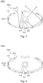
- the traceable optical device 100E of the embodiments as illustrated by Fig. 7 includes the two light guide members 110 and the two light sources 120, the traceable optical device 100E may have a greater total light output.
- the traceable optical device 100E can provide a traceable optical feature with a higher brightness contrast which can be easier to be identified.
- Fig. 8 is a schematic view of components in a traceable optical device (e.g., the traceable optical device 100A as shown in Figs. 2A-3 ) according to some embodiments of the present disclosure.
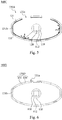
- the traceable optical device 100A may include one light guide member 110 and two light sources 120.
- the light guide member 110 has two light-incident surfaces 111 respectively at two ends E1, E2 of the light guide member 110.
- the light-incident surfaces 111 and the light-emitting surface 112 form an entire appearance of the light guide member 110.
- a greater luminous flux may be transmitted in the light guide member 110, and the light leaving the light-emitting surface 112 of the light guide member 110 may have a greater total light output, such that the traceable optical device 100A can provide a traceable optical feature with a higher brightness contrast which can be easier to be identified.
- Fig. 9 is a schematic view of a traceable optical device 100F according to some embodiments of the present disclosure.
- the traceable optical device 100F includes a light guide member 110, a light source 120, and a shielding member.
- the light guide member 110 and the light source 120 are identical or similar to those of the embodiments as illustrated by Figs. 2A-3 , therefore descriptions of these components are the same and would not be repeated here for simplicity.
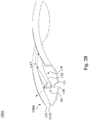
- the shielding member of the embodiments as illustrated by Fig. 9 includes a hollow housing 130F through which the light guide member 110 passes. That is, the light source 120 is outside the hollow housing 130F. As such, the light source 120 can be easily replaced with other kinds of light sources (e.g., the light sources of other colors) as needed.
- Fig. 10 is a schematic view of a traceable optical device 100G according to some embodiments of the present disclosure.
- the traceable optical device 100G includes a light guide member 110, a light source 120, and a shielding member.
- the light guide member 110 and the light source 120 are identical or similar to those of the embodiments as illustrated by Figs. 2A-3 , therefore descriptions of these components are the same and would not be repeated here for simplicity.
- the shielding member of the embodiments as illustrated by Fig. 10 includes a hollow housing 130G.
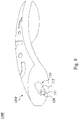
- the hollow housing 130G has an opening 131a' extending at a side surface thereof.
- the light-emitting surface 112 of the light guide member 110 is in contact with an edge of the opening 131a'. In other words, the light-emitting surface 112 of the light guide member 110 is close to the opening 131a', such that most of the light leaving the hollow housing 130G directly travels from the light-emitting surface 112 to the opening 131a'. In some embodiments, light-emitting surface 112 of the light guide member 110 may further seal the opening 131a'. As such, since a part of the light-emitting surface 112 forms a part of an appearance of the traceable optical device 100G, the traceable optical device 100G may have a low light loss and provide a traceable optical feature with the highest brightness contrast. In addition, dirt (e.g., dust or liquid) can be prevented from entering the hollow housing 130G by the light guide member 110.
- dirt e.g., dust or liquid
- Fig. 11 is a cross-sectional view of a traceable optical device 100H according to some embodiments of the present disclosure.
- the traceable optical device 100H includes a light guide member 110, a light source 120, and a shielding member.
- the light guide member 110, the light source 120, and the shielding member are identical or similar to those of the embodiments as illustrated by Figs. 2A-3 , therefore descriptions of these components are the same and would not be repeated here for simplicity.
- the shielding member of the embodiments as illustrated by Fig. 11 further includes a light distribution member 140 in the hollow housing 130A.
- the light distribution member 140 is connected to the light guide member 110 and optically coupled between the light-emitting surface 112 and the light transmission areas (i.e., the openings 131a). As discussed above, the light uniformly leaves the light-emitting surface 112 of the light guide member 110.
- the light distribution member 140 is configured to receive the light leaving the light-emitting surface 112 and evenly distribute the received light to each of the openings 131a. In detail, also according to the principle of total internal reflection, the light emitted from the light-emitting surface 112 of the light guide member 110 is transmitted forward through the light distribution member 140.
- the light distribution member 140 can more directly guide the light flux emitted from the light-emitting surface 112 of the light guide member 110 to the openings 131a.
- the light distribution member 140 may be made of a transparent material (e.g., plastic, polymer, glass, etc.).
- the light distribution member 140 includes a connecting portion 141 and a plurality of extending portions 142 connected to the connecting portion 141.
- the light distribution member 140 is detachably engaged with the light guide member 110 through the connecting portion 141.
- the connecting portion 141 has a recess 141a, and the light guide member 110 is accommodated in and engaged with the recess 141a, such that most of the light leaving the light-emitting surface 112 of the light guide member 110 may be received by the connecting portion 141 as far as possible.
- the extending portions 142 are extended from the connecting portion 141 to the openings 131a, respectively.
- extending portions 142 entirely fill the openings 131a, respectively, such that dirt (e.g., dust or liquid) can be prevented from entering the hollow housing 130A.
- the other surfaces of the light distribution member 140 may be coated with a reflective layer (e.g., a metal layer) to prevent light leakage.
- the light guide member 110 and the light distribution member 140 may be made of an identical material.
- the light guide member 110 and the light distribution member 140 form a unitary structure and have different refractive indices. In some embodiments, for unimpeded transmission of the luminous flux from the light guide member 110 to the light distribution member 140, the refractive index of the light guide member 110 is greater than the refractive index of the light distribution member 140.
- Fig. 12 is a schematic view of a traceable optical device 1001 according to some embodiments of the present disclosure.
- the traceable optical device 1001 includes a light guide member 110, a light source 120, and a shielding member.
- the light guide member 110 and the light source 120 are identical or similar to those of the embodiments as illustrated by Figs. 2A-3 , therefore descriptions of these components are the same and would not be repeated here for simplicity.
- the shielding member of the embodiments as illustrated by Fig. 11 is an opaque layer 1301 coated on the light-emitting surface 112 of the light guide member 110.
- the traceable optical device 1001 may have a low light loss and provide a traceable optical feature with the highest brightness contrast.
- the traceable optical device of the present disclosure after the light source emits light into the light guide member, the light can be transmitted in the light guide member and uniformly leave the light guide member from the light-emitting surface thereof.
- the light leaving the light guide member passes through the light transmission area of the shielding member to be detected.
- the traceable optical device can provide a traceable optical feature with high brightness contrast which can be easily identified, so that the location and/or orientation of the traceable optical device can be easily determined.
- the need to increase the number of the light source can be greatly reduced, so that the traceable optical device is low in electrical power loss.
Landscapes
- Engineering & Computer Science (AREA)
- Multimedia (AREA)
- Theoretical Computer Science (AREA)
- Human Computer Interaction (AREA)
- General Engineering & Computer Science (AREA)
- Physics & Mathematics (AREA)
- General Physics & Mathematics (AREA)
- Computer Hardware Design (AREA)
- Optics & Photonics (AREA)
- Computer Networks & Wireless Communication (AREA)
- Planar Illumination Modules (AREA)
- Optical Elements Other Than Lenses (AREA)
- Catching Or Destruction (AREA)
Abstract
Description
- The present disclosure relates to an electronic device, and more particularly, to a traceable optical device.
- One of the rapidly growing technologies in the field of human-computer interaction is various head-mounted displays (HMDs), which may be worn on a user's head and have one or two displays in front of the user's eyes. This type of display has multiple commercial applications involving simulation of virtual reality including video games, medicine, sport training, entertainment applications, and so forth. In the gaming field, these displays may be used, for example, to render three-dimensional (3D) virtual game worlds.
- Nowadays, computer vision methods, in particular, object tracking, are widely used in various applications. For example, object tracking may be used in a virtual reality (VR) system to detect the location of a handle held by a user. More specifically, the location and orientation of a handle can be determined by detecting feature points on the handle. However, when being held in front of a high-intensity light source in a dim environment, the feature points of the handle are always hard to be detected.
- Accordingly, it is an important issue for the industry to provide a traceable optical device capable of solving the aforementioned problems.
- An aspect of the disclosure is to provide a traceable optical device that can efficiently solve the aforementioned problems.
- According to an embodiment of the disclosure, a traceable optical device is capable of being tracked by an electronic device having an image sensor. The traceable optical device includes a light guide member, at least one light source, and a shielding member. The light guide member has at least one light-incident surface and a light-emitting surface connected to each other. The light source is configured to emit light into the light guide member from the light-incident surface. The shielding member shields the light guide member and has at least one light transmission area.
- In an embodiment of the disclosure, the shielding member includes a hollow housing. At least a part of the light guide member is in the hollow housing.
- In an embodiment of the disclosure, the light guide member and the light source are in the hollow housing.
- In an embodiment of the disclosure, the light source is outside the hollow housing.
- In an embodiment of the disclosure, the shielding member further includes a reflective layer on an inner surface of the hollow housing.
- In an embodiment of the disclosure, the shielding member further includes a light diffusion structure on an inner surface of the hollow housing.
- In an embodiment of the disclosure, the traceable optical device further includes a light distribution member in the hollow housing. The light distribution member is connected to the light guide member and optically coupled between the light-emitting surface and the light transmission area.
- In an embodiment of the disclosure, the light guide member and the light distribution member form a unitary structure and have different refractive indices.
- In an embodiment of the disclosure, a refractive index of the light guide member is greater than a refractive index of the light distribution member.
- In an embodiment of the disclosure, the light distribution member is detachably engaged with the light guide member.
- In an embodiment of the disclosure, the light guide member and the light distribution member are made of an identical material.
- In an embodiment of the disclosure, said at least one light transmission area is at least one opening of the hollow housing. The light distribution member fills the opening.
- In an embodiment of the disclosure, said at least one light transmission area is at least one opening of the hollow housing.
- In an embodiment of the disclosure, the light-emitting surface of the light guide member is in contact with an edge of the opening.
- In an embodiment of the disclosure, the light-emitting surface of the light guide member seals the opening.
- In an embodiment of the disclosure, the hollow housing includes a non-transparent part and at least one transparent part connected to each other. The transparent part serves as the light transmission area.
- In an embodiment of the disclosure, a number of said at least one light-incident surface and a number of said at least one light source are both two. The light sources are optically coupled to the light guide members respectively.
- In an embodiment of the disclosure, the light guide member is tubular and has two ends. The light-incident surfaces are respectively at the ends of the light guide member.
- In an embodiment of the disclosure, the shielding member is an opaque layer coated on the light-emitting surface of the light guide member.
- In an embodiment of the disclosure, the light-incident surface and the light-emitting surface form an entire appearance of the light guide member.
- Accordingly, in the traceable optical device of the present disclosure, after the light source emits light into the light guide member, the light can be transmitted in the light guide member and uniformly leave the light guide member from the light-emitting surface thereof. The light leaving the light guide member passes through the light transmission area of the shielding member to be detected. As such, the traceable optical device can provide a traceable optical feature with high brightness contrast which can be easily identified, so that the location and/or orientation of the traceable optical device can be easily determined. Moreover, by using the light guide member to transmit the light emitted from the light source and uniformly distribute the light leaving from the light-emitting surface thereof, the need to increase the number of the light source can be greatly reduced, so that the traceable optical device is low in electrical power loss.
- It is to be understood that both the foregoing general description and the following detailed description are by examples, and are intended to provide further explanation of the disclosure as claimed.
- The disclosure can be more fully understood by reading the following detailed description of the embodiment, with reference made to the accompanying drawings as follows:
-
Fig. 1 illustrates a user interacting with a head-mounted display (HMD) and a traceable optical device according to some embodiments of the present disclosure; -
Fig. 2A is a partial schematic view of a traceable optical device according to some embodiments of the present disclosure; -
Fig. 2B is another partial schematic view of the traceable optical device inFig. 2A according to some embodiments of the present disclosure; -
Fig. 3 is a cross-sectional view of a traceable optical device according to some embodiments of the present disclosure; -
Fig. 4 is a cross-sectional view of a traceable optical device according to some embodiments of the present disclosure; -
Fig. 5 is a cross-sectional view of a traceable optical device according to some embodiments of the present disclosure; -
Fig. 6 is a cross-sectional view of a traceable optical device according to some embodiments of the present disclosure; -
Fig. 7 is a cross-sectional view of a traceable optical device according to some embodiments of the present disclosure; -
Fig. 8 is a schematic view of components in a traceable optical device according to some embodiments of the present disclosure; -
Fig. 9 is a schematic view of a traceable optical device according to some embodiments of the present disclosure; -
Fig. 10 is a schematic view of a traceable optical device according to some embodiments of the present disclosure; -
Fig. 11 is a cross-sectional view of a traceable optical device according to some embodiments of the present disclosure; and -
Fig. 12 is a schematic view of a traceable optical device according to some embodiments of the present disclosure. - Reference will now be made in detail to the present embodiments of the disclosure, examples of which are illustrated in the accompanying drawings. Wherever possible, the same reference numbers are used in the drawings and the description to refer to the same or like parts. However, specific structural and functional details disclosed herein are merely representative for purposes of describing example embodiments, and thus may be embodied in many alternate forms and should not be construed as limited to only example embodiments set forth herein. Therefore, it should be understood that there is no intent to limit example embodiments to the particular forms disclosed, but on the contrary, example embodiments are to cover all modifications, equivalents, and alternatives falling within the scope of the disclosure.
- Reference is made to
Fig. 1. Fig. 1 illustrates a user interacting with a head-mounted display (HMD) 900 and a traceableoptical device 100A according to some embodiments of the present disclosure. In some embodiments, theHMD 900 may communicate wirelessly (e.g., WiFi, Bluetooth, etc.) with a computing device. In some embodiments, theHMD 900 may be wired directly to the computing device or in communication with the computing device via a network (e.g., the Internet). For example, the computing device may be a server on a network that provides game services. In some embodiments, theHMD 900 is a game playing device and the game is executed directly on theHMD 900, without the need of an external device to run the game. - In some embodiments, the
HMD 900 is equipped with acamera 910 thereon. Thecamera 910 may be a regular image camera, a stereo camera (i.e., with two or more lenses that capture images from the playing area), an infrared camera, a depth camera, a 3D camera, etc. Images taken by thecamera 910 may be processed to track the location and movement of the traceableoptical device 100A. The traceableoptical device 100A may be a one-handed controller illustrated inFig. 1 , but the disclosure is not limited in this regard. - In some embodiments, the user holds the traceable
optical device 100A. Thecamera 910 is used to track the location and movement of the traceableoptical device 100A, and operations related to the motion of the traceableoptical device 100A may be used as inputs for the game. For example, the traceableoptical device 100A may represent the handle of a sword, and the sword is displayed in the game scene. As the user moves the traceableoptical device 100A, the sword moves in the virtual world in synchronism with the traceableoptical device 100A. This way, the player is able to perform a fighting game operation where the sword is the weapon. In one embodiment, a relative position between theHMD 900 and the traceableoptical device 100A is calculated. The relative position is then used by the game to move a game object in synchronism with theHMD 900. - Reference is made to
Figs. 2A and2B .Fig. 2A is a partial schematic view of the traceableoptical device 100A according to some embodiments of the present disclosure.Fig. 2B is another partial schematic view of the traceableoptical device 100A inFig. 2A according to some embodiments of the present disclosure. The traceableoptical device 100A includes alight guide member 110, alight source 120, and a shielding member. Thelight guide member 110 has a light-incident surface 111 and a light-emittingsurface 112 connected to each other. Thelight source 120 is configured to emit light into thelight guide member 110 from the light-incident surface 111. The shielding member shields thelight guide member 110 and has a plurality of light transmission areas. - In some embodiments, as illustrated in
Figs. 2A and2B , the shielding member includes ahollow housing 130A. Thelight guide member 110 and thelight source 120 are in thehollow housing 130A. In some embodiments, thelight guide member 110 is tubular. The light-incident surface 111 is at an end E1 of thelight guide member 110. That is, the light-incident surface 111 is an end face of thelight guide member 110, and the light-emittingsurface 112 is a curved surface of thelight guide member 110 extended away from the end E1. In some embodiments, the light-incident surface 111 and the light-emittingsurface 112 form an entire appearance of thelight guide member 110. After thelight source 120 emits light into thelight guide member 110, the light can be transmitted in thelight guide member 110 and uniformly leave thelight guide member 110 from the light-emittingsurface 112 thereof. In detail, with the principle of total internal reflection, the luminous flux of thelight source 120 is continuously transmitted to the other end in thelight guide member 110. Thelight guide member 110 may be made of a transparent material (e.g., plastic, polymer, glass, etc.), so when the light does not satisfy the condition of total internal reflection, the light will be emitted from the light-emittingsurface 112 of thelight guide member 110. Thus, in addition to transmitting the luminous flux of thelight source 120, thelight guide member 110 also emits light over the entire light-emittingsurface 112. - In practice, some design parameters of the light guide member 110 (e.g., the angle of the light emitted by the
light source 120, the shape of thelight guide member 110, the material of thelight guide member 110, etc.) can be adjusted by the assistance of an optical simulation software, so as to let the light leave the light-emittingsurface 112 uniformly. - Reference is made to
Fig. 3. Fig. 3 is a cross-sectional view of the traceableoptical device 100A according to some embodiments of the present disclosure. As shown inFigs. 2A-3 , in some embodiments, thehollow housing 130A includes anon-transparent part 131, and the light transmission areas of the shielding member areopenings 131a of thenon-transparent part 131. In some embodiments, thenon-transparent part 131 may be made of an opaque material. In some other embodiments, thenon-transparent part 131 may be made of a transparent material with an opaque layer coated on theinner surface 131b (and/or an outer surface) of thenon-transparent part 131. After the light leaves thelight guide member 110 from the light-emittingsurface 112 thereof, some parts of the light may directly leave thehollow housing 130A through theopenings 131a to be detected, and some parts of the light may be reflected by aninner surface 131b of thenon-transparent part 131 one or more times before leaving thehollow housing 130A through theopenings 131a to be detected. As such, most of the light can be uniformly mixed in thehollow housing 130A before leaving thehollow housing 130A through theopenings 131a. - With the foregoing optical configurations, the traceable
optical device 100A can provide a traceable optical feature with high brightness contrast which can be easily identified, so that the location and/or orientation of the traceableoptical device 100A can be easily determined. Moreover, by using thelight guide member 110 to transmit the light emitted from thelight source 120 and uniformly distribute the light leaving from the light-emittingsurface 112 thereof, the need to increase the number of thelight source 120 can be greatly reduced, so that the traceableoptical device 100A is low in electrical power loss. - Reference is made to
Fig. 4. Fig. 4 is a cross-sectional view of a traceableoptical device 100B according to some embodiments of the present disclosure. As shown inFig. 4 , in some embodiments, the traceableoptical device 100B includes alight guide member 110, alight source 120, and a shielding member, and the shielding member includes ahollow housing 130A. Thelight guide member 110, thelight source 120, and thehollow housing 130A are identical or similar to those of the embodiments as illustrated byFigs. 2A-3 , therefore descriptions of these components are the same and would not be repeated here for simplicity. Compared to the embodiments as illustrated byFigs. 2A-3 , the shielding member of the embodiments as illustrated byFig. 4 further includes a reflective layer 132 on theinner surface 131b of thehollow housing 130A. As such, the light reflected in thehollow housing 130A can be more evenly mixed and has less light loss. In some embodiments, the reflective layer 132 may be a metal layer, but the disclosure is not limited in this regard. - Reference is made to
Fig. 5. Fig. 5 is a cross-sectional view of a traceableoptical device 100C according to some embodiments of the present disclosure. As shown inFig. 5 , in some embodiments, the traceableoptical device 100C includes alight guide member 110, alight source 120, and a shielding member, and the shielding member includes ahollow housing 130A. Thelight guide member 110, thelight source 120, and thehollow housing 130A are identical or similar to those of the embodiments as illustrated byFigs. 2A-3 , therefore descriptions of these components are the same and would not be repeated here for simplicity. Compared to the embodiments as illustrated byFigs. 2A-3 , the shielding member of the embodiments as illustrated byFig. 5 further includes alight diffusion structure 133 on theinner surface 131b of thehollow housing 130A. As such, the light reflected in thehollow housing 130A can be more evenly mixed. In some embodiments, thelight diffusion structure 133 may include a plurality of tiny protrusions (e.g., white dots) distributed on theinner surface 131b of thehollow housing 130A, but the disclosure is not limited in this regard. In some embodiments, theinner surface 131b of thehollow housing 130A may have a large surface roughness, so as to serve as thelight diffusion structure 133. In other words, thelight diffusion structure 133 may be an inner part of thehollow housing 130A. - Reference is made to
Fig. 6. Fig. 6 is a cross-sectional view of a traceableoptical device 100D according to some embodiments of the present disclosure. As shown inFig. 6 , in some embodiments, the traceableoptical device 100D includes alight guide member 110, alight source 120, and a shielding member. Thelight guide member 110 and thelight source 120 are identical or similar to those of the embodiments as illustrated byFigs. 2A-3 , therefore descriptions of these components are the same and would not be repeated here for simplicity. Compared to the embodiments as illustrated byFigs. 2A-3 , the shielding member of the embodiments as illustrated byFig. 6 includes ahollow housing 130D. Thehollow housing 130D includes anon-transparent part 131 and a plurality oftransparent parts 134 connected to each other. The transparent parts serve as the light transmission areas of the shielding member. That is, thehollow housing 130D has no opening, and the light reflected in thehollow housing 130D may leave thehollow housing 130D through thetransparent parts 134. As such, thelight guide member 110 and thelight source 120 may be sealed in thehollow housing 130D, so that dirt (e.g., dust or liquid) can be prevented from entering thehollow housing 130D. In some embodiments, thenon-transparent part 131 may be made of an opaque material. In some other embodiments, thenon-transparent part 131 and thetransparent parts 134 may be made of a transparent material with an opaque layer coated on theinner surface 131b (and/or an outer surface) of thenon-transparent part 131. In some embodiments, structures/textures/features may be added to a surface of thetransparent part 134 to increase light uniformity and to freely define the angle of diffusion. - Reference is made to
Fig. 7. Fig. 7 is a cross-sectional view of a traceableoptical device 100E according to some embodiments of the present disclosure. As shown inFig. 7 , in some embodiments, the traceableoptical device 100E includes twolight guide members 110, twolight sources 120, and a shielding member. Thelight sources 120 are optically coupled to thelight guide members 110 respectively. Thelight guide members 110, thelight sources 120, and the shielding member are identical or similar to those of the embodiments as illustrated byFigs. 2A-3 , therefore descriptions of these components are the same and would not be repeated here for simplicity. Compared to the embodiments as illustrated byFigs. 2A-3 , because the traceableoptical device 100E of the embodiments as illustrated byFig. 7 includes the twolight guide members 110 and the twolight sources 120, the traceableoptical device 100E may have a greater total light output. As such, the traceableoptical device 100E can provide a traceable optical feature with a higher brightness contrast which can be easier to be identified. - Reference is made to
Fig. 8. Fig. 8 is a schematic view of components in a traceable optical device (e.g., the traceableoptical device 100A as shown inFigs. 2A-3 ) according to some embodiments of the present disclosure. As shown inFigs. 2A and8 , in some embodiments, the traceableoptical device 100A may include onelight guide member 110 and twolight sources 120. Thelight guide member 110 has two light-incident surfaces 111 respectively at two ends E1, E2 of thelight guide member 110. The light-incident surfaces 111 and the light-emittingsurface 112 form an entire appearance of thelight guide member 110. As such, a greater luminous flux may be transmitted in thelight guide member 110, and the light leaving the light-emittingsurface 112 of thelight guide member 110 may have a greater total light output, such that the traceableoptical device 100A can provide a traceable optical feature with a higher brightness contrast which can be easier to be identified. - Reference is made to
Fig. 9. Fig. 9 is a schematic view of a traceableoptical device 100F according to some embodiments of the present disclosure. As shown inFig. 9 , in some embodiments, the traceableoptical device 100F includes alight guide member 110, alight source 120, and a shielding member. Thelight guide member 110 and thelight source 120 are identical or similar to those of the embodiments as illustrated byFigs. 2A-3 , therefore descriptions of these components are the same and would not be repeated here for simplicity. Compared to the embodiments as illustrated byFigs. 2A-3 , the shielding member of the embodiments as illustrated byFig. 9 includes ahollow housing 130F through which thelight guide member 110 passes. That is, thelight source 120 is outside thehollow housing 130F. As such, thelight source 120 can be easily replaced with other kinds of light sources (e.g., the light sources of other colors) as needed. - Reference is made to
Fig. 10. Fig. 10 is a schematic view of a traceableoptical device 100G according to some embodiments of the present disclosure. As shown inFig. 10 , in some embodiments, the traceableoptical device 100G includes alight guide member 110, alight source 120, and a shielding member. Thelight guide member 110 and thelight source 120 are identical or similar to those of the embodiments as illustrated byFigs. 2A-3 , therefore descriptions of these components are the same and would not be repeated here for simplicity. Compared to the embodiments as illustrated byFigs. 2A-3 , the shielding member of the embodiments as illustrated byFig. 10 includes ahollow housing 130G. Thehollow housing 130G has anopening 131a' extending at a side surface thereof. The light-emittingsurface 112 of thelight guide member 110 is in contact with an edge of theopening 131a'. In other words, the light-emittingsurface 112 of thelight guide member 110 is close to theopening 131a', such that most of the light leaving thehollow housing 130G directly travels from the light-emittingsurface 112 to theopening 131a'. In some embodiments, light-emittingsurface 112 of thelight guide member 110 may further seal theopening 131a'. As such, since a part of the light-emittingsurface 112 forms a part of an appearance of the traceableoptical device 100G, the traceableoptical device 100G may have a low light loss and provide a traceable optical feature with the highest brightness contrast. In addition, dirt (e.g., dust or liquid) can be prevented from entering thehollow housing 130G by thelight guide member 110. - Reference is made to
Fig. 11. Fig. 11 is a cross-sectional view of a traceableoptical device 100H according to some embodiments of the present disclosure. As shown inFig. 11 , in some embodiments, the traceableoptical device 100H includes alight guide member 110, alight source 120, and a shielding member. Thelight guide member 110, thelight source 120, and the shielding member are identical or similar to those of the embodiments as illustrated byFigs. 2A-3 , therefore descriptions of these components are the same and would not be repeated here for simplicity. Compared to the embodiments as illustrated byFigs. 2A-3 , the shielding member of the embodiments as illustrated byFig. 11 further includes alight distribution member 140 in thehollow housing 130A. Thelight distribution member 140 is connected to thelight guide member 110 and optically coupled between the light-emittingsurface 112 and the light transmission areas (i.e., theopenings 131a). As discussed above, the light uniformly leaves the light-emittingsurface 112 of thelight guide member 110. Thelight distribution member 140 is configured to receive the light leaving the light-emittingsurface 112 and evenly distribute the received light to each of theopenings 131a. In detail, also according to the principle of total internal reflection, the light emitted from the light-emittingsurface 112 of thelight guide member 110 is transmitted forward through thelight distribution member 140. Thelight distribution member 140 can more directly guide the light flux emitted from the light-emittingsurface 112 of thelight guide member 110 to theopenings 131a. In some embodiments, thelight distribution member 140 may be made of a transparent material (e.g., plastic, polymer, glass, etc.). - In some embodiments, the
light distribution member 140 includes a connectingportion 141 and a plurality of extendingportions 142 connected to the connectingportion 141. Thelight distribution member 140 is detachably engaged with thelight guide member 110 through the connectingportion 141. Specifically, the connectingportion 141 has arecess 141a, and thelight guide member 110 is accommodated in and engaged with therecess 141a, such that most of the light leaving the light-emittingsurface 112 of thelight guide member 110 may be received by the connectingportion 141 as far as possible. The extendingportions 142 are extended from the connectingportion 141 to theopenings 131a, respectively. In some embodiments, extendingportions 142 entirely fill theopenings 131a, respectively, such that dirt (e.g., dust or liquid) can be prevented from entering thehollow housing 130A. In some embodiments, in addition to the surface in contact with the light-emittingsurface 112 of thelight guide member 110 and the surfaces respectively exposed to theopenings 131a, the other surfaces of thelight distribution member 140 may be coated with a reflective layer (e.g., a metal layer) to prevent light leakage. In some embodiments, for unimpeded transmission of the luminous flux from thelight guide member 110 to thelight distribution member 140, thelight guide member 110 and thelight distribution member 140 may be made of an identical material. - In some embodiments, the
light guide member 110 and thelight distribution member 140 form a unitary structure and have different refractive indices. In some embodiments, for unimpeded transmission of the luminous flux from thelight guide member 110 to thelight distribution member 140, the refractive index of thelight guide member 110 is greater than the refractive index of thelight distribution member 140. - Reference is made to
Fig. 12. Fig. 12 is a schematic view of a traceableoptical device 1001 according to some embodiments of the present disclosure. As shown inFig. 12 , in some embodiments, the traceableoptical device 1001 includes alight guide member 110, alight source 120, and a shielding member. Thelight guide member 110 and thelight source 120 are identical or similar to those of the embodiments as illustrated byFigs. 2A-3 , therefore descriptions of these components are the same and would not be repeated here for simplicity. Compared to the embodiments as illustrated byFigs. 2A-3 , the shielding member of the embodiments as illustrated byFig. 11 is anopaque layer 1301 coated on the light-emittingsurface 112 of thelight guide member 110. As such, since a part of the light-emittingsurface 112 forms a part of an appearance of the traceableoptical device 1001, the traceableoptical device 1001 may have a low light loss and provide a traceable optical feature with the highest brightness contrast. - According to the foregoing recitations of the embodiments of the disclosure, it can be seen that in the traceable optical device of the present disclosure, after the light source emits light into the light guide member, the light can be transmitted in the light guide member and uniformly leave the light guide member from the light-emitting surface thereof. The light leaving the light guide member passes through the light transmission area of the shielding member to be detected. As such, the traceable optical device can provide a traceable optical feature with high brightness contrast which can be easily identified, so that the location and/or orientation of the traceable optical device can be easily determined. Moreover, by using the light guide member to transmit the light emitted from the light source and uniformly distribute the light leaving from the light-emitting surface thereof, the need to increase the number of the light source can be greatly reduced, so that the traceable optical device is low in electrical power loss.
- Although the present disclosure has been described in considerable detail with reference to certain embodiments thereof, other embodiments are possible. Therefore, the spirit and scope of the appended claims should not be limited to the description of the embodiments contained herein.
- It will be apparent to those skilled in the art that various modifications and variations can be made to the structure of the present disclosure without departing from the scope or spirit of the disclosure. In view of the foregoing, it is intended that the present disclosure cover modifications and variations of this disclosure provided they fall within the scope of the following claims.
Claims (15)
- A traceable optical device capable of being tracked by an electronic device having an image sensor, comprising:a light guide member having at least one light-incident surface and a light-emitting surface connected to each other;at least one light source configured to emit light into the light guide member from said at least one light-incident surface; anda shielding member shielding the light guide member and having at least one light transmission area.
- The traceable optical device of claim 1, wherein the shielding member comprises a hollow housing, and at least a part of the light guide member is in the hollow housing.
- The traceable optical device of claim 2, wherein the light guide member and said at least one light source are in the hollow housing.
- The traceable optical device of claim 2, wherein said at least one light source is outside the hollow housing.
- The traceable optical device of claim 2, wherein the shielding member further comprises a reflective layer or a light diffusion structure on an inner surface of the hollow housing.
- The traceable optical device of claim 2, further comprising a light distribution member in the hollow housing, wherein the light distribution member is connected to the light guide member and optically coupled between the light-emitting surface and said at least one light transmission area.
- The traceable optical device of claim 6, wherein the light guide member and the light distribution member form a unitary structure and have different refractive indices.
- The traceable optical device of claim 7, wherein a refractive index of the light guide member is greater than a refractive index of the light distribution member.
- The traceable optical device of claim 6, wherein the light distribution member is detachably engaged with the light guide member.
- The traceable optical device of claim 9, wherein said at least one light transmission area is at least one opening of the hollow housing, and the light distribution member fills said at least one opening.
- The traceable optical device of claim 2, wherein said at least one light transmission area is at least one opening of the hollow housing, and the light-emitting surface of the light guide member is in contact with an edge of said at least one opening.
- The traceable optical device of claim 2, wherein the hollow housing comprises a non-transparent part and at least one transparent part connected to each other, and said at least one transparent part serves as said at least one light transmission area.
- The traceable optical device of claim 1, wherein a number of said at least one light-incident surface and a number of said at least one light source are both two, and the light sources are optically coupled to the light guide members respectively.
- The traceable optical device of claim 13, wherein the light guide member is tubular and has two ends, and the light-incident surfaces are respectively at the ends of the light guide member.
- The traceable optical device of claim 1, wherein the shielding member is an opaque layer coated on the light-emitting surface of the light guide member.
Applications Claiming Priority (1)
| Application Number | Priority Date | Filing Date | Title |
|---|---|---|---|
| US201862635557P | 2018-02-27 | 2018-02-27 |
Publications (2)
| Publication Number | Publication Date |
|---|---|
| EP3531247A1 true EP3531247A1 (en) | 2019-08-28 |
| EP3531247B1 EP3531247B1 (en) | 2023-03-29 |
Family
ID=65628652
Family Applications (1)
| Application Number | Title | Priority Date | Filing Date |
|---|---|---|---|
| EP19159683.2A Active EP3531247B1 (en) | 2018-02-27 | 2019-02-27 | Traceable optical device |
Country Status (4)
| Country | Link |
|---|---|
| US (1) | US11181995B2 (en) |
| EP (1) | EP3531247B1 (en) |
| CN (1) | CN110193189B (en) |
| TW (1) | TWI705355B (en) |
Citations (5)
| Publication number | Priority date | Publication date | Assignee | Title |
|---|---|---|---|---|
| US20080261693A1 (en) * | 2008-05-30 | 2008-10-23 | Sony Computer Entertainment America Inc. | Determination of controller three-dimensional location using image analysis and ultrasonic communication |
| US8795078B1 (en) * | 2006-07-14 | 2014-08-05 | Ailive Inc. | Method and system providing compatibility between two different controllers |
| KR101483372B1 (en) * | 2013-10-07 | 2015-01-15 | 이금성 | Escape exit guidance lights |
| US20170192495A1 (en) * | 2015-12-30 | 2017-07-06 | Oculus Vr, Llc | Tracking constellation assembly for use in a virtual reality system |
| US20170354864A1 (en) * | 2016-06-11 | 2017-12-14 | Sony Interactive Entertainment Inc. | Directional Interface Object |
Family Cites Families (48)
| Publication number | Priority date | Publication date | Assignee | Title |
|---|---|---|---|---|
| US4996632A (en) * | 1988-10-07 | 1991-02-26 | Gulton Industries, Inc. | Multi-color illuminating system |
| JPH02174161A (en) * | 1988-12-26 | 1990-07-05 | Fuji Xerox Co Ltd | Image reading device |
| US5283772A (en) * | 1990-05-15 | 1994-02-01 | Sharp Kabushiki Kaisha | Optical head |
| US5796450A (en) * | 1994-12-16 | 1998-08-18 | Canon Kabushiki Kaisha | Illumination device and liquid crystal display apparatus including same |
| JP3551996B2 (en) * | 1995-08-25 | 2004-08-11 | 松下電器産業株式会社 | Medical laser probe |
| US6398778B1 (en) * | 1999-06-18 | 2002-06-04 | Photonics Research Ontario | Optical fiber diffuser |
| US7627139B2 (en) * | 2002-07-27 | 2009-12-01 | Sony Computer Entertainment Inc. | Computer image and audio processing of intensity and input devices for interfacing with a computer program |
| CA2398177A1 (en) * | 2002-08-14 | 2004-02-14 | Gilles Trudeau | Illuminating structure |
| US20040070965A1 (en) * | 2002-10-10 | 2004-04-15 | Bin-Tzer Lin | Removable light guide system for advertising display |
| US7559680B2 (en) * | 2003-09-04 | 2009-07-14 | Sensitile Systems Llc | Light system with stacked light pipe structure |
| US7131761B2 (en) * | 2003-09-13 | 2006-11-07 | Pipo Walter E | Self-illuminating fabricated solid material objects |
| FR2875993B1 (en) * | 2004-09-28 | 2006-12-08 | Thales Sa | ELECTROLUMINESCENT DIODE LIGHT BOX |
| JP5140922B2 (en) * | 2005-01-17 | 2013-02-13 | オムロン株式会社 | Light emitting light source and light emitting light source array |
| US8718437B2 (en) * | 2006-03-07 | 2014-05-06 | Qd Vision, Inc. | Compositions, optical component, system including an optical component, devices, and other products |
| US7386203B2 (en) * | 2005-06-30 | 2008-06-10 | Lawrence Livermore National Security, Llc | System for diffusing light from an optical fiber or light guide |
| US7588359B2 (en) * | 2005-09-26 | 2009-09-15 | Osram Sylvania Inc. | LED lamp with direct optical coupling in axial arrangement |
| CN101449309A (en) * | 2006-04-20 | 2009-06-03 | 株式会社藤仓 | Display device and its manufacturing method, pattern displaying method, and blind device and blind method |
| US7256899B1 (en) * | 2006-10-04 | 2007-08-14 | Ivan Faul | Wireless methods and systems for three-dimensional non-contact shape sensing |
| EP1995613A1 (en) * | 2007-05-21 | 2008-11-26 | Rohm and Haas Denmark Finance A/S | Mini Lightbar Illuminators For LCD Displays |
| EP2264560A1 (en) * | 2009-06-02 | 2010-12-22 | Koninklijke Philips Electronics N.V. | Appliance with luminous housing control depending on environment color |
| US8638549B2 (en) * | 2010-08-24 | 2014-01-28 | Apple Inc. | Electronic device display module |
| CN103238092A (en) * | 2010-12-04 | 2013-08-07 | 3M创新有限公司 | Lighting assembly and method of forming same |
| EP2742540B1 (en) * | 2011-08-08 | 2016-04-20 | Quarkstar, LLC | Illumination devices including multiple light emitting elements |
| US9116555B2 (en) * | 2011-11-23 | 2015-08-25 | Sony Computer Entertainment America Llc | Gaming controller |
| JP5913949B2 (en) * | 2011-12-13 | 2016-05-11 | オリンパス株式会社 | Light source system |
| JP2013123477A (en) * | 2011-12-13 | 2013-06-24 | Olympus Corp | Radiation module having plurality of light guide members |
| US9201452B2 (en) * | 2012-02-28 | 2015-12-01 | Apple Inc. | Electronic device with illuminated logo structures |
| WO2014074406A2 (en) * | 2012-11-07 | 2014-05-15 | Corning Incorporated | Films for display covers and display devices comprising the same |
| DE102012023190B4 (en) * | 2012-11-28 | 2018-10-31 | Balluff Gmbh | signal Tower |
| US9164032B2 (en) * | 2012-12-31 | 2015-10-20 | Omni Medsci, Inc. | Short-wave infrared super-continuum lasers for detecting counterfeit or illicit drugs and pharmaceutical process control |
| WO2014141391A1 (en) * | 2013-03-12 | 2014-09-18 | 堺ディスプレイプロダクト株式会社 | Light source device and display device |
| US20140340424A1 (en) * | 2013-05-17 | 2014-11-20 | Jeri J. Ellsworth | System and method for reconfigurable projected augmented/virtual reality appliance |
| JP6313432B2 (en) * | 2013-06-09 | 2018-04-18 | 株式会社ソニー・インタラクティブエンタテインメント | Head mounted display |
| WO2015104239A2 (en) * | 2014-01-07 | 2015-07-16 | Seereal Technologies S.A. | Display device for holographic reconstruction |
| MX2016010319A (en) * | 2014-02-10 | 2016-11-11 | Saint Gobain | Luminous glass assembly. |
| US20150355408A1 (en) * | 2014-06-10 | 2015-12-10 | Siriustek Incorporated | Illumination lamp having light guide bar |
| US9710711B2 (en) * | 2014-06-26 | 2017-07-18 | Adidas Ag | Athletic activity heads up display systems and methods |
| CN104299831B (en) * | 2014-09-24 | 2016-10-05 | 苏州达方电子有限公司 | The manufacture method of light-penetration key, transparent keycap and transparent keycap |
| EP3067449A1 (en) | 2015-03-10 | 2016-09-14 | SMR Patents S.à.r.l. | Light guide, lighting device and vehicle part |
| US10456685B2 (en) * | 2015-04-14 | 2019-10-29 | Nintendo Co., Ltd. | Identifying and tracking objects via lighting patterns |
| US10232770B2 (en) * | 2015-09-08 | 2019-03-19 | Ykk Corporation Of America | Illuminated marker |
| US20170273665A1 (en) * | 2016-03-28 | 2017-09-28 | Siemens Medical Solutions Usa, Inc. | Pose Recovery of an Ultrasound Transducer |
| WO2017169641A1 (en) * | 2016-03-29 | 2017-10-05 | 株式会社齋藤創造研究所 | Input device and image display system |
| CN106598260A (en) * | 2017-02-06 | 2017-04-26 | 上海青研科技有限公司 | Eyeball-tracking device, VR (Virtual Reality) equipment and AR (Augmented Reality) equipment by use of eyeball-tracking device |
| TWM552879U (en) * | 2017-08-04 | 2017-12-11 | Depo Auto Parts Ind Co Ltd | Device making text and figure luminescent |
| CN107510439A (en) * | 2017-09-25 | 2017-12-26 | 北京我爱购科技发展有限公司 | A kind of photoelectric detection system and physiological information detection device |
| JP2019132914A (en) * | 2018-01-29 | 2019-08-08 | キヤノン株式会社 | Illumination device and camera system including teh same |
| US10962701B2 (en) * | 2019-04-04 | 2021-03-30 | S.V.V. Technology Innovations, Inc. | Wide-area solid-state illumination devices and systems |
-
2019
- 2019-02-27 US US16/286,598 patent/US11181995B2/en active Active
- 2019-02-27 TW TW108106877A patent/TWI705355B/en active
- 2019-02-27 EP EP19159683.2A patent/EP3531247B1/en active Active
- 2019-02-27 CN CN201910146554.5A patent/CN110193189B/en active Active
Patent Citations (5)
| Publication number | Priority date | Publication date | Assignee | Title |
|---|---|---|---|---|
| US8795078B1 (en) * | 2006-07-14 | 2014-08-05 | Ailive Inc. | Method and system providing compatibility between two different controllers |
| US20080261693A1 (en) * | 2008-05-30 | 2008-10-23 | Sony Computer Entertainment America Inc. | Determination of controller three-dimensional location using image analysis and ultrasonic communication |
| KR101483372B1 (en) * | 2013-10-07 | 2015-01-15 | 이금성 | Escape exit guidance lights |
| US20170192495A1 (en) * | 2015-12-30 | 2017-07-06 | Oculus Vr, Llc | Tracking constellation assembly for use in a virtual reality system |
| US20170354864A1 (en) * | 2016-06-11 | 2017-12-14 | Sony Interactive Entertainment Inc. | Directional Interface Object |
Non-Patent Citations (1)
| Title |
|---|
| ANONYMOUS: "JIT Catalog R1", 16 August 2007 (2007-08-16), XP055603425, Retrieved from the Internet <URL:https://sites.google.com/site/jitdownload/JITCatalog-R1.zip?attredirects=0> [retrieved on 20190708] * |
Also Published As
| Publication number | Publication date |
|---|---|
| CN110193189A (en) | 2019-09-03 |
| CN110193189B (en) | 2022-09-13 |
| US11181995B2 (en) | 2021-11-23 |
| TWI705355B (en) | 2020-09-21 |
| TW201937346A (en) | 2019-09-16 |
| US20190302905A1 (en) | 2019-10-03 |
| EP3531247B1 (en) | 2023-03-29 |
Similar Documents
| Publication | Publication Date | Title |
|---|---|---|
| US10521026B2 (en) | Passive optical and inertial tracking in slim form-factor | |
| JP2022551550A (en) | Artificial reality system with Bragg grating | |
| US10146335B2 (en) | Modular extension of inertial controller for six DOF mixed reality input | |
| US9710973B2 (en) | Low-latency fusing of virtual and real content | |
| US8884984B2 (en) | Fusing virtual content into real content | |
| JP5879353B2 (en) | Head position and orientation tracking | |
| US10254846B1 (en) | Systems and methods to facilitate interactions with virtual content in an augmented reality environment | |
| US11507201B2 (en) | Virtual reality | |
| US20130328925A1 (en) | Object focus in a mixed reality environment | |
| US20140368534A1 (en) | Concurrent optimal viewing of virtual objects | |
| CA2914012A1 (en) | Shared and private holographic objects | |
| US20110149043A1 (en) | Device and method for displaying three-dimensional images using head tracking | |
| US20240264660A1 (en) | Facilitating User Interface Interactions in an Artificial Reality Environment | |
| US20240201456A1 (en) | Thin illumination layer waveguide and methods of fabrication | |
| US20240012244A1 (en) | OPTICAL ASSEMBLY WITH MICRO LIGHT EMITTING DIODE (LED) AS EYE-TRACKING NEAR INFRARED (nIR) ILLUMINATION SOURCE | |
| CN110007462B (en) | head mounted display | |
| US20240069347A1 (en) | System and method using eye tracking illumination | |
| US11181995B2 (en) | Traceable optical device | |
| US20250278316A1 (en) | Systems and methods to extend an interactive space across multiple platforms | |
| JPWO2019189868A1 (en) | Head mounted display | |
| US20250037621A1 (en) | Systems and methods for providing sensing and lighting to maintain real nose perception in virtual reality | |
| EP4425304A2 (en) | Radar-assisted three-dimensional (3d) detection for near-eye display devices | |
| KR20150084510A (en) | Wearable display device | |
| CN110732133A (en) | method and device for remotely controlling game view angle based on intelligent glasses | |
| CN118631982A (en) | Line-of-sight (LoS) communication capabilities for near-eye display devices |
Legal Events
| Date | Code | Title | Description |
|---|---|---|---|
| PUAI | Public reference made under article 153(3) epc to a published international application that has entered the european phase |
Free format text: ORIGINAL CODE: 0009012 |
|
| STAA | Information on the status of an ep patent application or granted ep patent |
Free format text: STATUS: REQUEST FOR EXAMINATION WAS MADE |
|
| STAA | Information on the status of an ep patent application or granted ep patent |
Free format text: STATUS: EXAMINATION IS IN PROGRESS |
|
| 17P | Request for examination filed |
Effective date: 20190227 |
|
| AK | Designated contracting states |
Kind code of ref document: A1 Designated state(s): AL AT BE BG CH CY CZ DE DK EE ES FI FR GB GR HR HU IE IS IT LI LT LU LV MC MK MT NL NO PL PT RO RS SE SI SK SM TR |
|
| AX | Request for extension of the european patent |
Extension state: BA ME |
|
| 17Q | First examination report despatched |
Effective date: 20190808 |
|
| RBV | Designated contracting states (corrected) |
Designated state(s): AL AT BE BG CH CY CZ DE DK EE ES FI FR GB GR HR HU IE IS IT LI LT LU LV MC MK MT NL NO PL PT RO RS SE SI SK SM TR |
|
| GRAP | Despatch of communication of intention to grant a patent |
Free format text: ORIGINAL CODE: EPIDOSNIGR1 |
|
| RIC1 | Information provided on ipc code assigned before grant |
Ipc: G02B 27/01 20060101ALN20221005BHEP Ipc: G08C 23/04 20060101ALI20221005BHEP Ipc: G06F 3/0346 20130101ALI20221005BHEP Ipc: G06F 1/16 20060101ALI20221005BHEP Ipc: A63F 13/833 20140101ALI20221005BHEP Ipc: A63F 13/26 20140101ALI20221005BHEP Ipc: A63F 13/24 20140101ALI20221005BHEP Ipc: A63F 13/213 20140101ALI20221005BHEP Ipc: G06F 3/033 20130101ALI20221005BHEP Ipc: G06F 3/03 20060101ALI20221005BHEP Ipc: G06F 3/01 20060101AFI20221005BHEP |
|
| STAA | Information on the status of an ep patent application or granted ep patent |
Free format text: STATUS: GRANT OF PATENT IS INTENDED |
|
| RIC1 | Information provided on ipc code assigned before grant |
Ipc: G02B 27/01 20060101ALN20221021BHEP Ipc: G08C 23/04 20060101ALI20221021BHEP Ipc: G06F 3/0346 20130101ALI20221021BHEP Ipc: G06F 1/16 20060101ALI20221021BHEP Ipc: A63F 13/833 20140101ALI20221021BHEP Ipc: A63F 13/26 20140101ALI20221021BHEP Ipc: A63F 13/24 20140101ALI20221021BHEP Ipc: A63F 13/213 20140101ALI20221021BHEP Ipc: G06F 3/033 20130101ALI20221021BHEP Ipc: G06F 3/03 20060101ALI20221021BHEP Ipc: G06F 3/01 20060101AFI20221021BHEP |
|
| INTG | Intention to grant announced |
Effective date: 20221110 |
|
| GRAS | Grant fee paid |
Free format text: ORIGINAL CODE: EPIDOSNIGR3 |
|
| GRAA | (expected) grant |
Free format text: ORIGINAL CODE: 0009210 |
|
| STAA | Information on the status of an ep patent application or granted ep patent |
Free format text: STATUS: THE PATENT HAS BEEN GRANTED |
|
| AK | Designated contracting states |
Kind code of ref document: B1 Designated state(s): AL AT BE BG CH CY CZ DE DK EE ES FI FR GB GR HR HU IE IS IT LI LT LU LV MC MK MT NL NO PL PT RO RS SE SI SK SM TR |
|
| REG | Reference to a national code |
Ref country code: CH Ref legal event code: EP |
|
| REG | Reference to a national code |
Ref country code: AT Ref legal event code: REF Ref document number: 1557146 Country of ref document: AT Kind code of ref document: T Effective date: 20230415 |
|
| REG | Reference to a national code |
Ref country code: DE Ref legal event code: R096 Ref document number: 602019026791 Country of ref document: DE |
|
| REG | Reference to a national code |
Ref country code: NL Ref legal event code: FP Ref country code: IE Ref legal event code: FG4D |
|
| REG | Reference to a national code |
Ref country code: DE Ref legal event code: R082 Ref document number: 602019026791 Country of ref document: DE |
|
| REG | Reference to a national code |
Ref country code: LT Ref legal event code: MG9D |
|
| PG25 | Lapsed in a contracting state [announced via postgrant information from national office to epo] |
Ref country code: RS Free format text: LAPSE BECAUSE OF FAILURE TO SUBMIT A TRANSLATION OF THE DESCRIPTION OR TO PAY THE FEE WITHIN THE PRESCRIBED TIME-LIMIT Effective date: 20230329 Ref country code: NO Free format text: LAPSE BECAUSE OF FAILURE TO SUBMIT A TRANSLATION OF THE DESCRIPTION OR TO PAY THE FEE WITHIN THE PRESCRIBED TIME-LIMIT Effective date: 20230629 Ref country code: LV Free format text: LAPSE BECAUSE OF FAILURE TO SUBMIT A TRANSLATION OF THE DESCRIPTION OR TO PAY THE FEE WITHIN THE PRESCRIBED TIME-LIMIT Effective date: 20230329 Ref country code: LT Free format text: LAPSE BECAUSE OF FAILURE TO SUBMIT A TRANSLATION OF THE DESCRIPTION OR TO PAY THE FEE WITHIN THE PRESCRIBED TIME-LIMIT Effective date: 20230329 Ref country code: HR Free format text: LAPSE BECAUSE OF FAILURE TO SUBMIT A TRANSLATION OF THE DESCRIPTION OR TO PAY THE FEE WITHIN THE PRESCRIBED TIME-LIMIT Effective date: 20230329 |
|
| REG | Reference to a national code |
Ref country code: AT Ref legal event code: MK05 Ref document number: 1557146 Country of ref document: AT Kind code of ref document: T Effective date: 20230329 |
|
| PG25 | Lapsed in a contracting state [announced via postgrant information from national office to epo] |
Ref country code: SE Free format text: LAPSE BECAUSE OF FAILURE TO SUBMIT A TRANSLATION OF THE DESCRIPTION OR TO PAY THE FEE WITHIN THE PRESCRIBED TIME-LIMIT Effective date: 20230329 Ref country code: GR Free format text: LAPSE BECAUSE OF FAILURE TO SUBMIT A TRANSLATION OF THE DESCRIPTION OR TO PAY THE FEE WITHIN THE PRESCRIBED TIME-LIMIT Effective date: 20230630 Ref country code: FI Free format text: LAPSE BECAUSE OF FAILURE TO SUBMIT A TRANSLATION OF THE DESCRIPTION OR TO PAY THE FEE WITHIN THE PRESCRIBED TIME-LIMIT Effective date: 20230329 |
|
| PG25 | Lapsed in a contracting state [announced via postgrant information from national office to epo] |
Ref country code: SM Free format text: LAPSE BECAUSE OF FAILURE TO SUBMIT A TRANSLATION OF THE DESCRIPTION OR TO PAY THE FEE WITHIN THE PRESCRIBED TIME-LIMIT Effective date: 20230329 Ref country code: RO Free format text: LAPSE BECAUSE OF FAILURE TO SUBMIT A TRANSLATION OF THE DESCRIPTION OR TO PAY THE FEE WITHIN THE PRESCRIBED TIME-LIMIT Effective date: 20230329 Ref country code: PT Free format text: LAPSE BECAUSE OF FAILURE TO SUBMIT A TRANSLATION OF THE DESCRIPTION OR TO PAY THE FEE WITHIN THE PRESCRIBED TIME-LIMIT Effective date: 20230731 Ref country code: ES Free format text: LAPSE BECAUSE OF FAILURE TO SUBMIT A TRANSLATION OF THE DESCRIPTION OR TO PAY THE FEE WITHIN THE PRESCRIBED TIME-LIMIT Effective date: 20230329 Ref country code: EE Free format text: LAPSE BECAUSE OF FAILURE TO SUBMIT A TRANSLATION OF THE DESCRIPTION OR TO PAY THE FEE WITHIN THE PRESCRIBED TIME-LIMIT Effective date: 20230329 Ref country code: AT Free format text: LAPSE BECAUSE OF FAILURE TO SUBMIT A TRANSLATION OF THE DESCRIPTION OR TO PAY THE FEE WITHIN THE PRESCRIBED TIME-LIMIT Effective date: 20230329 |
|
| PG25 | Lapsed in a contracting state [announced via postgrant information from national office to epo] |
Ref country code: SK Free format text: LAPSE BECAUSE OF FAILURE TO SUBMIT A TRANSLATION OF THE DESCRIPTION OR TO PAY THE FEE WITHIN THE PRESCRIBED TIME-LIMIT Effective date: 20230329 Ref country code: PL Free format text: LAPSE BECAUSE OF FAILURE TO SUBMIT A TRANSLATION OF THE DESCRIPTION OR TO PAY THE FEE WITHIN THE PRESCRIBED TIME-LIMIT Effective date: 20230329 Ref country code: IS Free format text: LAPSE BECAUSE OF FAILURE TO SUBMIT A TRANSLATION OF THE DESCRIPTION OR TO PAY THE FEE WITHIN THE PRESCRIBED TIME-LIMIT Effective date: 20230729 |
|
| REG | Reference to a national code |
Ref country code: DE Ref legal event code: R097 Ref document number: 602019026791 Country of ref document: DE |
|
| PG25 | Lapsed in a contracting state [announced via postgrant information from national office to epo] |
Ref country code: DK Free format text: LAPSE BECAUSE OF FAILURE TO SUBMIT A TRANSLATION OF THE DESCRIPTION OR TO PAY THE FEE WITHIN THE PRESCRIBED TIME-LIMIT Effective date: 20230329 Ref country code: CZ Free format text: LAPSE BECAUSE OF FAILURE TO SUBMIT A TRANSLATION OF THE DESCRIPTION OR TO PAY THE FEE WITHIN THE PRESCRIBED TIME-LIMIT Effective date: 20230329 |
|
| PLBE | No opposition filed within time limit |
Free format text: ORIGINAL CODE: 0009261 |
|
| STAA | Information on the status of an ep patent application or granted ep patent |
Free format text: STATUS: NO OPPOSITION FILED WITHIN TIME LIMIT |
|
| 26N | No opposition filed |
Effective date: 20240103 |
|
| PG25 | Lapsed in a contracting state [announced via postgrant information from national office to epo] |
Ref country code: SI Free format text: LAPSE BECAUSE OF FAILURE TO SUBMIT A TRANSLATION OF THE DESCRIPTION OR TO PAY THE FEE WITHIN THE PRESCRIBED TIME-LIMIT Effective date: 20230329 |
|
| PG25 | Lapsed in a contracting state [announced via postgrant information from national office to epo] |
Ref country code: SI Free format text: LAPSE BECAUSE OF FAILURE TO SUBMIT A TRANSLATION OF THE DESCRIPTION OR TO PAY THE FEE WITHIN THE PRESCRIBED TIME-LIMIT Effective date: 20230329 Ref country code: IT Free format text: LAPSE BECAUSE OF FAILURE TO SUBMIT A TRANSLATION OF THE DESCRIPTION OR TO PAY THE FEE WITHIN THE PRESCRIBED TIME-LIMIT Effective date: 20230329 |
|
| PG25 | Lapsed in a contracting state [announced via postgrant information from national office to epo] |
Ref country code: MC Free format text: LAPSE BECAUSE OF FAILURE TO SUBMIT A TRANSLATION OF THE DESCRIPTION OR TO PAY THE FEE WITHIN THE PRESCRIBED TIME-LIMIT Effective date: 20230329 |
|
| REG | Reference to a national code |
Ref country code: CH Ref legal event code: PL |
|
| PG25 | Lapsed in a contracting state [announced via postgrant information from national office to epo] |
Ref country code: LU Free format text: LAPSE BECAUSE OF NON-PAYMENT OF DUE FEES Effective date: 20240227 |
|
| PG25 | Lapsed in a contracting state [announced via postgrant information from national office to epo] |
Ref country code: CH Free format text: LAPSE BECAUSE OF NON-PAYMENT OF DUE FEES Effective date: 20240229 |
|
| PG25 | Lapsed in a contracting state [announced via postgrant information from national office to epo] |
Ref country code: LU Free format text: LAPSE BECAUSE OF NON-PAYMENT OF DUE FEES Effective date: 20240227 Ref country code: CH Free format text: LAPSE BECAUSE OF NON-PAYMENT OF DUE FEES Effective date: 20240229 |
|
| PG25 | Lapsed in a contracting state [announced via postgrant information from national office to epo] |
Ref country code: BG Free format text: LAPSE BECAUSE OF FAILURE TO SUBMIT A TRANSLATION OF THE DESCRIPTION OR TO PAY THE FEE WITHIN THE PRESCRIBED TIME-LIMIT Effective date: 20230329 |
|
| PG25 | Lapsed in a contracting state [announced via postgrant information from national office to epo] |
Ref country code: BG Free format text: LAPSE BECAUSE OF FAILURE TO SUBMIT A TRANSLATION OF THE DESCRIPTION OR TO PAY THE FEE WITHIN THE PRESCRIBED TIME-LIMIT Effective date: 20230329 |
|
| REG | Reference to a national code |
Ref country code: BE Ref legal event code: MM Effective date: 20240229 |
|
| PG25 | Lapsed in a contracting state [announced via postgrant information from national office to epo] |
Ref country code: BE Free format text: LAPSE BECAUSE OF NON-PAYMENT OF DUE FEES Effective date: 20240229 |
|
| PGFP | Annual fee paid to national office [announced via postgrant information from national office to epo] |
Ref country code: FR Payment date: 20241231 Year of fee payment: 7 |
|
| PG25 | Lapsed in a contracting state [announced via postgrant information from national office to epo] |
Ref country code: IE Free format text: LAPSE BECAUSE OF NON-PAYMENT OF DUE FEES Effective date: 20240227 |
|
| PG25 | Lapsed in a contracting state [announced via postgrant information from national office to epo] |
Ref country code: IE Free format text: LAPSE BECAUSE OF NON-PAYMENT OF DUE FEES Effective date: 20240227 Ref country code: BE Free format text: LAPSE BECAUSE OF NON-PAYMENT OF DUE FEES Effective date: 20240229 |
|
| PGFP | Annual fee paid to national office [announced via postgrant information from national office to epo] |
Ref country code: NL Payment date: 20250108 Year of fee payment: 7 |
|
| PGFP | Annual fee paid to national office [announced via postgrant information from national office to epo] |
Ref country code: DE Payment date: 20241231 Year of fee payment: 7 |
|
| PGFP | Annual fee paid to national office [announced via postgrant information from national office to epo] |
Ref country code: GB Payment date: 20250102 Year of fee payment: 7 |
|
| PG25 | Lapsed in a contracting state [announced via postgrant information from national office to epo] |
Ref country code: CY Free format text: LAPSE BECAUSE OF FAILURE TO SUBMIT A TRANSLATION OF THE DESCRIPTION OR TO PAY THE FEE WITHIN THE PRESCRIBED TIME-LIMIT; INVALID AB INITIO Effective date: 20190227 |
|
| PG25 | Lapsed in a contracting state [announced via postgrant information from national office to epo] |
Ref country code: HU Free format text: LAPSE BECAUSE OF FAILURE TO SUBMIT A TRANSLATION OF THE DESCRIPTION OR TO PAY THE FEE WITHIN THE PRESCRIBED TIME-LIMIT; INVALID AB INITIO Effective date: 20190227 |
|
| PG25 | Lapsed in a contracting state [announced via postgrant information from national office to epo] |
Ref country code: TR Free format text: LAPSE BECAUSE OF FAILURE TO SUBMIT A TRANSLATION OF THE DESCRIPTION OR TO PAY THE FEE WITHIN THE PRESCRIBED TIME-LIMIT Effective date: 20230329 |