EP3528387A1 - A led driver circuit, corresponding device and method - Google Patents
A led driver circuit, corresponding device and method Download PDFInfo
- Publication number
- EP3528387A1 EP3528387A1 EP19155623.2A EP19155623A EP3528387A1 EP 3528387 A1 EP3528387 A1 EP 3528387A1 EP 19155623 A EP19155623 A EP 19155623A EP 3528387 A1 EP3528387 A1 EP 3528387A1
- Authority
- EP
- European Patent Office
- Prior art keywords
- led driver
- devices
- driver devices
- chain
- slave address
- Prior art date
- Legal status (The legal status is an assumption and is not a legal conclusion. Google has not performed a legal analysis and makes no representation as to the accuracy of the status listed.)
- Granted
Links
Images

Classifications
-
- H—ELECTRICITY
- H03—ELECTRONIC CIRCUITRY
- H03K—PULSE TECHNIQUE
- H03K7/00—Modulating pulses with a continuously-variable modulating signal
- H03K7/08—Duration or width modulation ; Duty cycle modulation
-
- G—PHYSICS
- G06—COMPUTING OR CALCULATING; COUNTING
- G06F—ELECTRIC DIGITAL DATA PROCESSING
- G06F13/00—Interconnection of, or transfer of information or other signals between, memories, input/output devices or central processing units
- G06F13/38—Information transfer, e.g. on bus
- G06F13/42—Bus transfer protocol, e.g. handshake; Synchronisation
- G06F13/4282—Bus transfer protocol, e.g. handshake; Synchronisation on a serial bus, e.g. I2C bus, SPI bus
- G06F13/4291—Bus transfer protocol, e.g. handshake; Synchronisation on a serial bus, e.g. I2C bus, SPI bus using a clocked protocol
-
- H—ELECTRICITY
- H05—ELECTRIC TECHNIQUES NOT OTHERWISE PROVIDED FOR
- H05B—ELECTRIC HEATING; ELECTRIC LIGHT SOURCES NOT OTHERWISE PROVIDED FOR; CIRCUIT ARRANGEMENTS FOR ELECTRIC LIGHT SOURCES, IN GENERAL
- H05B45/00—Circuit arrangements for operating light-emitting diodes [LED]
-
- G—PHYSICS
- G06—COMPUTING OR CALCULATING; COUNTING
- G06F—ELECTRIC DIGITAL DATA PROCESSING
- G06F2213/00—Indexing scheme relating to interconnection of, or transfer of information or other signals between, memories, input/output devices or central processing units
- G06F2213/0016—Inter-integrated circuit (I2C)
-
- G—PHYSICS
- G06—COMPUTING OR CALCULATING; COUNTING
- G06F—ELECTRIC DIGITAL DATA PROCESSING
- G06F2213/00—Indexing scheme relating to interconnection of, or transfer of information or other signals between, memories, input/output devices or central processing units
- G06F2213/0052—Assignment of addresses or identifiers to the modules of a bus system
Definitions
- the description relates to LED driver circuits.
- One or more embodiments may apply to arrangements wherein a microcontroller is intended to co-operate with a plurality of LED drivers.
- a desirable feature in (e.g., integrated) circuits for driving LEDs is the ability for a user to start simultaneously and maintain the synchronization of the channels in a set of LED driver devices coupled, e.g. in a star or chain topology.
- LED drivers may use dedicated pins in order to facilitate synchronization of the various devices.
- a reduced number of pins used for that purpose would represent a desirable feature.
- An object of one or more embodiments is to contribute in pursuing a reduction of the number of pins in such arrangements without this reduction being detrimental to operation.
- One or more embodiments may relate to a corresponding device, e.g. a circuit as discussed previously coupled to a set of LED sources driven thereby.
- One or more embodiments may relate to a corresponding method.
- One or more embodiments facilitate coupling in a star or chain topology a number of LED driver devices (e.g., N such devices) with a simultaneous start-up capability of their LED channels obtained by means of a microcontroller without dedicated synchronization pins, thereby reducing the number of pins involved.
- a number of LED driver devices e.g., N such devices
- One or more embodiments may provide an architecture for an integrated LED driver circuit which facilitates simultaneously switching-on of channels of a plurality of LED driver devices.
- One or more embodiments facilitate automatic synchronization of the PWM patterns from a plurality of LED drivers connected, e.g., in a chain arrangement by dispensing with the use of dedicated synchronization pins.
- One or more embodiments make it possible, for each one of a plurality of LED driver devices, to reconfigure some LED driver input-output pins (IOs) used to assign a local I2C address to each LED driver with the capability of using a single clock signal either from a LED driver master device in a chain connection or from an external clock source.
- IOs LED driver input-output pins
- a LED driver can be configured as a master or slave unit via an I2C bus by means of its local I2C address.
- various LED drivers in a set can be started simultaneously by means of an I2C (global) address.
- the various LED drivers can then be addressed individually by e.g. a microcontroller by using the local I2C slave address of each LED driver, so that the configuration of the channels in each LED driver can be changed as desired.
- references to "an embodiment” or “one embodiment” in the framework of the present description is intended to indicate that a particular configuration, structure, or characteristic described in relation to the embodiment is comprised in at least one embodiment.
- phrases such as “in an embodiment” or “in one embodiment” that may be present in one or more points of the present description do not necessarily refer to one and the same embodiment.
- particular conformations, structures, or characteristics may be combined in any adequate way in one or more embodiments.
- One or more embodiments as exemplified herein refer to a circuit arrangement wherein an (external) microcontroller (see, e.g., MC in Figure 2 ) may start-up (different) channels in a number (e.g. N) LED drivers simultaneously.
- an (external) microcontroller see, e.g., MC in Figure 2
- One or more embodiments may involve reconfiguring some "non-dedicated" LED driver input/output pins (IOs) used to assign respective local I2C addresses to the N LED drivers in order to facilitate exploiting a single clock signal from a LED driver master device in a chain (or from an external clock source) thereby dispensing with dedicated synchronization input and output pins for each of the N LED drivers.
- IOs LED driver input/output pins
- FIG. 1 a circuit arrangement is exemplified including a number N of LED drivers referred to as #1, #2, ... and so on.
- N While a generic number N of such devices may be present in embodiments, in the representations of Figure 1 and Figure 2 only two such devices (#1 and #2, in Figure 1 ) or four devices (#1, #2, #3 and #4, in Figure 2 ) are visible for simplicity.
- each of the devices #1, #2, ... includes Ax pins which can be used to assign a dedicated local slave address to each device.
- pins are coupled to a pin address latching (local slave add) circuit block 10 via respective signal paths 12, 14.
- these signal paths can be exploited as signal paths for propagating clock signals.
- the signal path 12 may extend towards the pin (node) A0 from a multiplexer (MUX OUT) 16 controlled via a signal chain_out_en. While a simple representation is provided to facilitate understanding, such a selector may include a multi-bit mux selector. For instance, in the presence of four inputs, the selector may include two bits.
- the multiplexer (MUX OUT) 16 facilitates selecting one of its inputs coupled to an oscillator 18 producing an oscillator output signal osc_out, with the oscillator 18 enabled via a signal EN (which, as discussed in the following, can be provided by means of a global slave address).
- the signal path 14 may extend from the pin A1 towards another multiplexer (MUX IN) 20 controlled via a signal chain_in_en and having an input coupled to the signal osc_out from the oscillator 18.
- MUX IN multiplexer
- the output from the multiplexer 20 (that is, either the signal osc_out or the signal from A1), depending on the signal chain_in_en, is supplied to a finite state machine (FSM) 22.
- FSM finite state machine
- the FSM 22 is enabled by the signal EN (to be discussed in the following) and may receive the signal osc_out from the oscillator 18 or from pin A1 (depending on the value of signal chain_in_en) to provide output drive channels CHx (1 to n) for respective LED arrangement L1, L2, ..., which per se may be distinct elements from the embodiments.
- these signals can be generated (in a manner known per se) in the microcontroller MC and transferred to the driver devices #1,#2, ..., e.g. over the bus I2C bus. Corresponding signal paths may not be visible in the figures for the sake of simplicity of illustration.
- EN, chain_in_en, chain_out_en may be configuration bits of the LED driver device which can be programmed by the microcontroller MC via the bus I2C, while en_A0 and en_A1 can be configured in order that the pins A0 and A1 are configured as input; when chain_out_en is set via I2C, en_A0 can be automatically set to configure pin A0 as an output.
- the pin A1 can be (always) configured as an input, so that signal en_A1 is (always) reset, other than, e.g., in a LED driver device test/debug mode where certain internal signals can be brought out on A1.
- pin A0 which (see, e.g., the diagram of Figure 1 ) can be used to bring out certain internal signals in a test/debug mode of the device.
- Embodiments as exemplified herein comprise two pins A0 and A1, so that up to four devices can be addressed through an associated bus (top portion in both Figures 1 and 2 ).
- An I2C will hereinafter exemplified as a possible bus option having an internal slave address for use in one or more embodiments.
- N LED driver devices e.g. #1, #2, ..., #N
- one or more embodiments may apply to N LED driver devices coupled in a "star" topology.
- the clock output on A0 from a master device can be applied (simultaneously) to the A1 pins in the slave devices (e.g., #2, #3, ).
- the pins A0 will be used (only) for address definition and will not be used for conveying to A0 the (master) clock from A1. In other words, the signal path 12 through the multiplexer 16 will not be enabled.
- pins such as A0 and A1 can be used to assign internal I2C local Slave Addresses to N led driver devices #1, #2, ..., #N.
- the A0 and A1 pins can be connected to general purpose input/outputs (IOs) in e.g. a microcontroller MC (see Figure 2 ) which facilitates configuring the I2C local slave address in each of N LED driver devices #1, #2, ..., #N.
- IOs general purpose input/outputs
- the microcontroller master I2C bus is connected, by means of I2C bus clock (SCL) and data (SDA) lines with SDA and SCL pins in the N LED driver devices.
- SCL and SDA are well-known acronyms for Serial CLock and Serial DAta, respectively.
- the I2C bus comprises pull-up resistors Rp according to I2C standards.
- the microcontroller MC may configure its own general purpose IOs in order to drive the 10 port A and the IO port C to VDD and the IO port B to GND.
- the microcontroller MC may also configure the LED driver device #4 as slave, by programming via I2C, using the I2C local slave address of the LED driver device #4 (bit 0 chain_in_en of a daisy chain register - see Figure 4 ).
- the input of the multiplexer 20 (see Figure 1 ) in the LED driver device #4 will be the signal coming from its A1 pin.
- Setting bit 0 chain_in_en in the LED driver device #4 implies that the pin address latching block 10 will latch its A0 and A1 values and provide them to its I2C interface, instead of providing these information from pin A0 and A1, with LED driver #4 pin A1 now configured as input for the clock as a result of the en_A1 signal driven low.
- the microcontroller MC may configure in the same way the LED driver devices #2 and #3 as slave devices, by programming via I2C (again using the I2C local slave addresses in the LED driver devices #2 and #3), bit 0 chain_in_en of daisy chain register (see Figure 4 ).
- the input of the multiplexer 20 (see Figure 1 ) in the LED driver devices #2 and #3 will be the signal coming from the respective A1 pin.
- Setting bit 0 chain_in_en in the LED driver devices #2 and #3 implies that the pin address latching block 10 therein will latch its A0 and A1 values and provide them to its I2C interface, instead of providing that information from the pins A0 and A1, with the pin A1 in LED driver #2 and LED driver #3 now configured as an input for the clock, e.g., by means of the en_A1 signal driven low.
- the slave devices #2, #3 and #4 will have their slave address information coming from their respective A0, A1 pins latched internally by the block 10.
- the microcontroller MC will thus be in a position to release the I/O port A (I/O ports in High-Z condition) in order to be used further for clock propagation from the master device #1, by relying on the fact that, from that point on, the slave devices #2, #3 and #4 will respond with their respective I2C local addresses, e.g. 59h, 5Bh and 5Ah.
- the microcontroller MC will configure the LED driver devices #2 and #3 (again using the I2C local slave addresses for devices #2 and #3), bit 1 chain_out_en of the daisy chain register (see Figure 4 ).
- the output of the multiplexer 16 (see Figure 1 ) of the LED driver devices #2 and #3 will be the signal coming from the A1 pin with the LED driver device #1 adapted to be configured as a master device.
- the microcontroller MC may configure the LED driver device #1, again by programming via I2C by using the I2C local slave address, bit 1 chain_out_en.
- a further (last) step may involve releasing the I/O port B (I/O port in High-Z condition) in order to enable a clock path between the master device #1 and the slave device #2.
- the I2C global slave address may be an I2C address recognized as a valid address by all the (e.g., N) LED drivers coupled to I2C.
- the master device e.g., #1 in the exemplary case discussed here
- Each one of the N-1 slave LED driver device (e.g., #2, ..., #N) will from now operate (time) aligned with the master LED driver device #1.
- one or more embodiments may involve reconfiguring some "non-dedicated" LED driver input/output pins (IOs) used to assign respective local I2C addresses to the N LED drivers in order to facilitate exploiting a single clock signal thereby dispensing with dedicated synchronization input and output pins for each of the N LED drivers.
- IOs LED driver input/output pins
- each and every LED driver device e.g., #1, #2, ... may retain its capability of operating in a "stand-alone” mode, by exploiting for that purpose the respective internal oscillator 18 that can be activated via the signal (bit) EN, programmable via the I2C bus.
- the programming bit EN can be written individually in each device, e.g., #1, #2, ..., by using its own slave address (e.g., 58H, 59H, 5AH, 5BH).
- such "global" EN signal may turn on the FSMs in the LED driver devices #1, #2, ..., with the FSMs in the slave devices #2, #3, ... exploiting the clock signal received from the master device #1.
- the programming bits chain_in_en can be set, e.g., to "1" with chain_out_en also set, e.g. to "1".
- the multiplexer 16 in the slave devices # 2, #3, ... will propagate towards A0 - in the place of the signal from the respective internal oscillator 18 - the output from the multiplexer 20 which in turn will obtain the clock signal from the "previous" device in the chain as received at the input A1.
- the (single) clock propagated from the device #1 has been assumed to be the clock signal from the oscillator 18 in that device (e.g., #1).
- the "master" configuration of, e.g. device #1 can be adopted (possibly in a selective, programmable manner) when exploiting the clock produced by its internal oscillator 18 as a clock signal for the chain of devices.
- the single clock signal propagated over the chain can be sourced (as a possible alternative to the clock signal generated by the oscillator 18 in the device #1) from an external clock EXT CLK sourced - in any known manner - as schematically exemplified in Figure 2 .
- a line coupled to, e.g., the D port of the microcontroller MC. This may be coupled to ground (e.g. according to the diagram of Figure 1 ).
- that line can be at first coupled to ground and then switched to a desired frequency conveying the external clock to the device #1 which at this point can be configured as slave device receiving the clock signal EXT CLK via the pin A1.
- the global enable may be set as a step following configuration of the devices.
- the source of EXT CLK can be, e.g. a high-accuracy clock source already available to the circuit exemplified for other purposes.
- the device #1 will eventually share the same "slave” configuration of the other devices, #2, #3, ... and thus accept the external clock source EXT CLK as input on pin A1 and transmit that clock signal to the "subsequent" device (e.g., device #2) on pin A0.
- said one LED driver device (#1) in the set of LED driver devices may have said first slave address pin configured to receive an external clock signal (e.g., RXT CLK in Figure 2 ) and couple said external clock signal to the finite state machine in said one LED driver device in the set of LED driver devices via the first signal path between the first slave address pin and the finite state machine in said one LED driver device in the set of LED driver devices.
- an external clock signal e.g., RXT CLK in Figure 2
- the finite state machine in said one LED driver device in the set of LED driver devices may be coupled to the oscillator in said one LED driver device in the set of LED driver devices to receive the clock signal (e.g. osc_out) generated thereby.
- the clock signal e.g. osc_out
- the controller may have has a set of (e.g. general-purpose input/output nodes, such as A, B, C) each coupled to the second slave address pin of one of the devices in the set of LED driver devices and to the first slave address pin of another one of the devices in the set of LED driver devices.
- a set of e.g. general-purpose input/output nodes, such as A, B, C
- the controller may be configured to provide over via said bus a global bus address (e.g. EN) to the LED driver devices in the set of LED driver devices, said global bus address configured to be set alternatively to a first one resp. a second one binary value to provide coordinated activation, resp. de-activation, of the finite state machines in the LED driver devices in the set of LED driver devices.
- a global bus address e.g. EN
- the LED driver devices in the set of LED driver devices may comprise respective pin address latching blocks (e.g., 10) configured to latch values for said at least one first and one second slave address pins and provide such latched values to said bus via said bus pins coupled to said bus.
- respective pin address latching blocks e.g., 10
- a device e.g. an automotive light
Landscapes
- Engineering & Computer Science (AREA)
- Theoretical Computer Science (AREA)
- Physics & Mathematics (AREA)
- General Engineering & Computer Science (AREA)
- General Physics & Mathematics (AREA)
- Control Of Indicators Other Than Cathode Ray Tubes (AREA)
- Control Of El Displays (AREA)
- Selective Calling Equipment (AREA)
- Optical Communication System (AREA)
Abstract
Description
- The description relates to LED driver circuits.
- One or more embodiments may apply to arrangements wherein a microcontroller is intended to co-operate with a plurality of LED drivers.
- A desirable feature in (e.g., integrated) circuits for driving LEDs is the ability for a user to start simultaneously and maintain the synchronization of the channels in a set of LED driver devices coupled, e.g. in a star or chain topology.
- These LED drivers may use dedicated pins in order to facilitate synchronization of the various devices. In certain applications, e.g. low-cost and/or small devices, a reduced number of pins used for that purpose would represent a desirable feature.
- An object of one or more embodiments is to contribute in pursuing a reduction of the number of pins in such arrangements without this reduction being detrimental to operation.
- According to one or more embodiments, such an object can be achieved by means of a circuit having the features set forth in the claims that follow.
- One or more embodiments may relate to a corresponding device, e.g. a circuit as discussed previously coupled to a set of LED sources driven thereby.
- One or more embodiments may relate to a corresponding method.
- The claims are an integral part of the technical teaching provided herein in respect of embodiments.
- One or more embodiments facilitate coupling in a star or chain topology a number of LED driver devices (e.g., N such devices) with a simultaneous start-up capability of their LED channels obtained by means of a microcontroller without dedicated synchronization pins, thereby reducing the number of pins involved.
- One or more embodiments may provide an architecture for an integrated LED driver circuit which facilitates simultaneously switching-on of channels of a plurality of LED driver devices.
- One or more embodiments facilitate automatic synchronization of the PWM patterns from a plurality of LED drivers connected, e.g., in a chain arrangement by dispensing with the use of dedicated synchronization pins.
- One or more embodiments make it possible, for each one of a plurality of LED driver devices, to reconfigure some LED driver input-output pins (IOs) used to assign a local I2C address to each LED driver with the capability of using a single clock signal either from a LED driver master device in a chain connection or from an external clock source.
- In one or more embodiments, a LED driver can be configured as a master or slave unit via an I2C bus by means of its local I2C address.
- In one or more embodiments, various LED drivers in a set can be started simultaneously by means of an I2C (global) address.
- In one or more embodiments, once started simultaneously via an I2C global address recognized by all the LED driver devices in a set, the various LED drivers, can then be addressed individually by e.g. a microcontroller by using the local I2C slave address of each LED driver, so that the configuration of the channels in each LED driver can be changed as desired.
- One or more embodiments will now be described, by way of example only, with reference to the annexed figures, wherein:
-
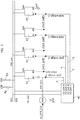
Figure 1 is an exemplary circuit diagram of embodiments, -
Figure 2 is a block diagram exemplary of certain possible features of embodiments, -
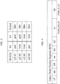
Figures 3 and 4 are exemplary of possible configurations in embodiments. - In the ensuing description, one or more specific details are illustrated, aimed at providing an in-depth understanding of examples of embodiments of this description. The embodiments may be obtained without one or more of the specific details, or with other methods, components, materials, etc. In other cases, known structures, materials, or operations are not illustrated or described in detail so that certain aspects of embodiments will not be obscured.
- Reference to "an embodiment" or "one embodiment" in the framework of the present description is intended to indicate that a particular configuration, structure, or characteristic described in relation to the embodiment is comprised in at least one embodiment. Hence, phrases such as "in an embodiment" or "in one embodiment" that may be present in one or more points of the present description do not necessarily refer to one and the same embodiment. Moreover, particular conformations, structures, or characteristics may be combined in any adequate way in one or more embodiments.
- The references used herein are provided merely for convenience and hence do not define the extent of protection or the scope of the embodiments.
- One or more embodiments as exemplified herein refer to a circuit arrangement wherein an (external) microcontroller (see, e.g., MC in
Figure 2 ) may start-up (different) channels in a number (e.g. N) LED drivers simultaneously. - One or more embodiments may involve reconfiguring some "non-dedicated" LED driver input/output pins (IOs) used to assign respective local I2C addresses to the N LED drivers in order to facilitate exploiting a single clock signal from a LED driver master device in a chain (or from an external clock source) thereby dispensing with dedicated synchronization input and output pins for each of the N LED drivers.
- In
Figure 1 a circuit arrangement is exemplified including a number N of LED drivers referred to as #1, #2, ... and so on. - While a generic number N of such devices may be present in embodiments, in the representations of
Figure 1 andFigure 2 only two such devices (#1 and #2, inFigure 1 ) or four devices (#1, #2, #3 and #4, inFigure 2 ) are visible for simplicity. - As exemplified herein, each of the
devices # 1, #2, ... includes Ax pins which can be used to assign a dedicated local slave address to each device. - These pins (two of them, labeled A0 and A1, are considered here by way of example) are coupled to a pin address latching (local slave add)
circuit block 10 viarespective signal paths - As discussed in the following, in one or more embodiments, these signal paths can be exploited as signal paths for propagating clock signals.
- As exemplified herein, the
signal path 12 may extend towards the pin (node) A0 from a multiplexer (MUX OUT) 16 controlled via a signal chain_out_en. While a simple representation is provided to facilitate understanding, such a selector may include a multi-bit mux selector. For instance, in the presence of four inputs, the selector may include two bits. - As exemplified herein, the multiplexer (MUX OUT) 16 facilitates selecting one of its inputs coupled to an
oscillator 18 producing an oscillator output signal osc_out, with theoscillator 18 enabled via a signal EN (which, as discussed in the following, can be provided by means of a global slave address). - As exemplified herein, the
signal path 14 may extend from the pin A1 towards another multiplexer (MUX IN) 20 controlled via a signal chain_in_en and having an input coupled to the signal osc_out from theoscillator 18. - The output from the multiplexer 20 (that is, either the signal osc_out or the signal from A1), depending on the signal chain_in_en, is supplied to a finite state machine (FSM) 22.
- The FSM 22 is enabled by the signal EN (to be discussed in the following) and may receive the signal osc_out from the
oscillator 18 or from pin A1 (depending on the value of signal chain_in_en) to provide output drive channels CHx (1 to n) for respective LED arrangement L1, L2, ..., which per se may be distinct elements from the embodiments. - Save for the points discussed in the following - the structure of the various
drive devices # 1, #2, ..., #N as exemplified herein is conventional in the art, thus making it unnecessary to provide a more detailed description herein. - This applies, e.g., to the arrangements which facilitate generation of various control signals (EN, en_A0, en_A1, chain_in_en, chain_out_en, and so on) applied to the
driver devices # 1, #2, ... as discussed in the following. - In one or more embodiments, these signals can be generated (in a manner known per se) in the microcontroller MC and transferred to the
driver devices # 1,#2, ..., e.g. over the bus I2C bus. Corresponding signal paths may not be visible in the figures for the sake of simplicity of illustration. - For instance, EN, chain_in_en, chain_out_en may be configuration bits of the LED driver device which can be programmed by the microcontroller MC via the bus I2C, while en_A0 and en_A1 can be configured in order that the pins A0 and A1 are configured as input; when chain_out_en is set via I2C, en_A0 can be automatically set to configure pin A0 as an output.
- The pin A1 can be (always) configured as an input, so that signal en_A1 is (always) reset, other than, e.g., in a LED driver device test/debug mode where certain internal signals can be brought out on A1.
- The same points apply, mutatis mutandis, to the pin A0, which (see, e.g., the diagram of
Figure 1 ) can be used to bring out certain internal signals in a test/debug mode of the device. - Taken per se, these can again represent conventional options in the art.
- Also, it will be appreciated that one or more embodiments are not intended to be used imperatively with device structures as exemplified herein.
- As discussed in the following, in one or more embodiments the possibility may exist of:
- configuring one of the devices (e.g., the device #1) as a master device, wherein the chain_in_en selector is set, e.g., to "0" and the output osc_out from the (internal)
oscillator 18 propagates through themultiplexer 20; - configuring the other devices (e.g., the
devices # 2, #3, ...) as slave devices wherein the chain_in_en selector is set to "1" and the signal from the pin A1 propagates through themultiplexer 20. - For each N led driver device, Ax pins, where x= log2 (N), are used to assign a dedicated local Slave Address to each
device # 1, #2, ..., #N. - Embodiments as exemplified herein comprise two pins A0 and A1, so that up to four devices can be addressed through an associated bus (top portion in both
Figures 1 and2 ). - An I2C will hereinafter exemplified as a possible bus option having an internal slave address for use in one or more embodiments.
- Of course the possibility exists of addressing a higher number of devices. For instance, document
US 9 275 000 B2 - While a chain connection of N LED driver devices (
e.g. # 1, #2, ..., #N) is exemplified herein, one or more embodiments may apply to N LED driver devices coupled in a "star" topology. - In a star topology, the clock output on A0 from a master device (e.g., #1, as discussed in the following) can be applied (simultaneously) to the A1 pins in the slave devices (e.g., #2, #3, ...). In the case of a star topology the pins A0 will be used (only) for address definition and will not be used for conveying to A0 the (master) clock from A1. In other words, the
signal path 12 through themultiplexer 16 will not be enabled. - In the following, a further detailed description will be provided in respect of embodiments involving a chain topology, insofar as the same concepts disclosed adapted to be applied to a star topology as discussed above.
- As noted, in a multiple device connection, pins such as A0 and A1 can be used to assign internal I2C local Slave Addresses to N led
driver devices # 1, #2, ..., #N. - To that effect, the A0 and A1 pins can be connected to general purpose input/outputs (IOs) in e.g. a microcontroller MC (see
Figure 2 ) which facilitates configuring the I2C local slave address in each of N LEDdriver devices # 1, #2, ..., #N. - In one or more embodiments as exemplified herein, the microcontroller master I2C bus is connected, by means of I2C bus clock (SCL) and data (SDA) lines with SDA and SCL pins in the N LED driver devices. In this context, SCL and SDA are well-known acronyms for Serial CLock and Serial DAta, respectively.
- In one or more embodiments as exemplified herein, the I2C bus comprises pull-up resistors Rp according to I2C standards.
- In one or more embodiments as exemplified herein, at start-up, the microcontroller MC may configure its own general purpose IOs in order to drive the 10 port A and the IO port C to VDD and the IO port B to GND.
- In one or more possible embodiments as exemplified in
Figure 2 : - the IO port A may be connected to the A0 pin of the
LED driver # 2 and to the A1 pin of theLED driver # 3; - the IO port C may be connected to the A0 pin of the
LED driver # 3 and to the A1 pin of theLED driver # 4; - the IO port B may be connected to the A0 pin of the
LED driver # 1 and to the A1 pin of theLED driver # 2. - These IO port connections facilitate assigning to each one of the N LED driver devices a local slave address of its own as summarized in the table of
Figure 3 . - The microcontroller MC may also configure the LED
driver device # 4 as slave, by programming via I2C, using the I2C local slave address of the LED driver device #4 (bit 0 chain_in_en of a daisy chain register - seeFigure 4 ). - In that way, the input of the multiplexer 20 (see
Figure 1 ) in the LEDdriver device # 4 will be the signal coming from its A1 pin. Settingbit 0 chain_in_en in the LEDdriver device # 4 implies that the pinaddress latching block 10 will latch its A0 and A1 values and provide them to its I2C interface, instead of providing these information from pin A0 and A1, withLED driver # 4 pin A1 now configured as input for the clock as a result of the en_A1 signal driven low. - The microcontroller MC may configure in the same way the LED
driver devices # 2 and #3 as slave devices, by programming via I2C (again using the I2C local slave addresses in the LEDdriver devices # 2 and #3),bit 0 chain_in_en of daisy chain register (seeFigure 4 ). - In that way, the input of the multiplexer 20 (see
Figure 1 ) in the LEDdriver devices # 2 and #3 will be the signal coming from the respective A1 pin. - Setting
bit 0 chain_in_en in the LEDdriver devices # 2 and #3 implies that the pinaddress latching block 10 therein will latch its A0 and A1 values and provide them to its I2C interface, instead of providing that information from the pins A0 and A1, with the pin A1 inLED driver # 2 andLED driver # 3 now configured as an input for the clock, e.g., by means of the en_A1 signal driven low. - At this point, the
slave devices # 2, #3 and #4 will have their slave address information coming from their respective A0, A1 pins latched internally by theblock 10. - The microcontroller MC will thus be in a position to release the I/O port A (I/O ports in High-Z condition) in order to be used further for clock propagation from the
master device # 1, by relying on the fact that, from that point on, theslave devices # 2, #3 and #4 will respond with their respective I2C local addresses, e.g. 59h, 5Bh and 5Ah. - As a further act, in order to enable clock paths between
slave devices # 2 and #3 and betweenslave devices # 3 and #4, the microcontroller MC will configure the LEDdriver devices # 2 and #3 (again using the I2C local slave addresses fordevices # 2 and #3),bit 1 chain_out_en of the daisy chain register (seeFigure 4 ). - In that way, the output of the multiplexer 16 (see
Figure 1 ) of the LEDdriver devices # 2 and #3 will be the signal coming from the A1 pin with the LEDdriver device # 1 adapted to be configured as a master device. - For instance, the microcontroller MC may configure the LED
driver device # 1, again by programming via I2C by using the I2C local slave address,bit 1 chain_out_en. - Such an act will not produce any conflict between the A0 pin of the LED
driver device # 1 and the I/O port B of the microcontroller MC, with the A0 output carrying out GND (at that point of time, the internal oscillator ofdevice # 1 is still disabled) and port B forced to GND. - A further (last) step may involve releasing the I/O port B (I/O port in High-Z condition) in order to enable a clock path between the
master device # 1 and theslave device # 2. - It will be appreciated that setting I/O port lines free does not imply that each one of the N LED devices will be unable to respond to its own local address: thanks to the pin
address latching block 10, the initial information provided by the microcontroller MC by means of the A0 and A1 pins will be latched internally of each one of the N LED driver devices. These devices will thus be able to answer over I2C at the respective I2C local slave address for forwarding on-the-fly channel configurations from the microcontroller MC. - The system will now be ready to be started simultaneously by setting EN=1 (enable signal to the oscillator 18) by means of an I2C Global Slave Address (5Ch, but this can be chosen differently) on all
devices # 1, #2, ..., #N. - As noted, the I2C global slave address may be an I2C address recognized as a valid address by all the (e.g., N) LED drivers coupled to I2C.
- In the LED driver device #1 (namely, the master device) the EN=1 bit being set e.g. by means of an I2C global address will activate the
oscillator 18 and theFSM 22. - Conversely, in the other LED
driver devices # 2, ..., #N (namely, the slave devices), setting chain_in_en=1 may lead to theoscillator 18 therein remaining inactive insofar as the associated circuitry may exploit the clock signal applied on the input A1 via clock path 14-20: e.g., theFSMs 22 will start-up and operate with the oscillator clock of the master device (e.g., #1 in the exemplary case discussed here) coming from their A1 pins. - Each one of the N-1 slave LED driver device (e.g., #2, ..., #N) will from now operate (time) aligned with the master LED
driver device # 1. - Also, generation of PWM signals from the
FMSs 22 can be halted simultaneously by setting EN=0 for all devices e.g., by means of the I2C global address. - As noted at the outset of this description, one or more embodiments may involve reconfiguring some "non-dedicated" LED driver input/output pins (IOs) used to assign respective local I2C addresses to the N LED drivers in order to facilitate exploiting a single clock signal thereby dispensing with dedicated synchronization input and output pins for each of the N LED drivers.
- It will be otherwise appreciated that, in one or more embodiments, along with the coupling (e.g., a "daisy-chain" connection) to other identical devices as exemplified in the figures, each and every LED driver device, e.g., #1, #2, ... may retain its capability of operating in a "stand-alone" mode, by exploiting for that purpose the respective
internal oscillator 18 that can be activated via the signal (bit) EN, programmable via the I2C bus. - In addition to enabling the
internal oscillator 18 such a signal may also be exploited to enable other circuitry including the channels to which the LED units L1, L2, ... may be connected. - The programming bit EN can be written individually in each device, e.g., #1, #2, ..., by using its own slave address (e.g., 58H, 59H, 5AH, 5BH).
- This may be the case when a single, individual LED
driver device # 1, #2, ..., is intended to be turned on or when all the LEDdriver devices # 1, #2, ..., are intended to be turned on the same time, which may occur via a "global" slave address recognized by all the LED driver devices connected to the I2C communication bus. This may result in a simultaneous activation of alldriver devices # 1, #2, ..., connected to the I2C bus and the LED units L1, L2, ... driven thereby. - Conversely, as a result of adopting the coupling (e.g., a "daisy-chain" connection) exemplified herein such "global" EN signal may turn on the FSMs in the LED
driver devices # 1, #2, ..., with the FSMs in theslave devices # 2, #3, ... exploiting the clock signal received from themaster device # 1. - In one or more embodiments, in those devices configured as slaves (e.g., # 2, #3, ...) the programming bits chain_in_en can be set, e.g., to "1" with chain_out_en also set, e.g. to "1". In that case, the
multiplexer 16 in theslave devices # 2, #3, ... will propagate towards A0 - in the place of the signal from the respective internal oscillator 18 - the output from themultiplexer 20 which in turn will obtain the clock signal from the "previous" device in the chain as received at the input A1. - The last slave device in the chain (e.g.,
slave device # 4 inFigure 2 ) will have chain_in_en = 1 and chain_out_en = 0 and therefore will accept on input A1 the clock coming fromslave # 3 without propagating it to output on A0 viaMUX 16. - Throughout the detailed description of exemplary embodiments provided herein so far the (single) clock propagated from the
device # 1 has been assumed to be the clock signal from theoscillator 18 in that device (e.g., #1). - Stated otherwise, in certain embodiments, the "master" configuration of,
e.g. device # 1, can be adopted (possibly in a selective, programmable manner) when exploiting the clock produced by itsinternal oscillator 18 as a clock signal for the chain of devices. - In certain embodiments, the single clock signal propagated over the chain can be sourced (as a possible alternative to the clock signal generated by the
oscillator 18 in the device #1) from an external clock EXT CLK sourced - in any known manner - as schematically exemplified inFigure 2 . - For instance, the possibility exists of providing a line coupled to, e.g., the D port of the microcontroller MC. This may be coupled to ground (e.g. according to the diagram of
Figure 1 ). - In one or more embodiments that line can be at first coupled to ground and then switched to a desired frequency conveying the external clock to the
device # 1 which at this point can be configured as slave device receiving the clock signal EXT CLK via the pin A1. - In that case, the global enable may be set as a step following configuration of the devices. As exemplified herein, the external oscillator providing the signal EXT CLK may be enabled via a signal en_CLK_EXT. This facilitates applying that clock signal to the pin A1 of the first device (e.g. #1) only after configuration thereof (setting of chain_in_en=1 and chain_out_en=1), that is only after the microcontroller MC has released the line D, which goes to High-Z. This facilitates avoiding conflicts on the D line of the controller.
- Stated otherwise, after the
device # 1 has been configured with chain_in_en=1 e chain_out_en=1, the external clock source can be enabled by setting en_CLK_EXT=1 and then the global enable can be set, e.g., to "1" via the bus I2C. - The source of EXT CLK can be, e.g. a high-accuracy clock source already available to the circuit exemplified for other purposes.
- In that case, the
device # 1 will eventually share the same "slave" configuration of the other devices, #2, #3, ... and thus accept the external clock source EXT CLK as input on pin A1 and transmit that clock signal to the "subsequent" device (e.g., device #2) on pin A0. - As noted previously, the concepts and operating principles described herein in connection with a chain topology will apply mutatis mutandis to a star topology as considered in the foregoing.
- In a circuit according to one or more embodiments:
- i) the circuit may comprise a set of LED driver devices (e.g., #1, #2, ...) comprising a finite state machine (e.g., 22) configured to generate LED drive PWM-modulated signal patterns (e.g., CHx) as well as an oscillator (e.g., 18) generating a clock signal (e.g., osc_out) for the finite state machine;
- ii) the LED driver devices in the set of LED driver devices may be coupled (e.g., SDA, SCL) via a bus (e.g. I2C bus), the LED driver devices in the set of LED driver devices having bus pins (e.g., I2C) coupled to said bus as well a set of slave address pins comprising at least one first (e.g., A1) and one second (e.g., A0) slave address pin,
- iii) the LED driver devices in the set of LED driver devices may comprise:
- a first signal path (e.g., 14, 20) activatable (e.g., en_A1, chain_in_en) between the first slave address pin and the finite state machine;
- a second signal path (e.g., 12, 16) activatable (e.g., en_A0, chain_out_en) between the finite state machine and the second slave address pin,
- iv) the circuit may comprise a controller (e.g. MC) having a set of (e.g. general-purpose input/output nodes such as A, B, C) coupled to the slave address pins in the LED driver devices in the set of LED driver devices, wherein the controller may be configured to:
- provide via the slave address pins of the LED driver devices in the set of LED driver devices at least one inter-device clock signal propagation path from the second slave address pin in one (e.g., #1) LED driver device in the set of LED driver devices to the first slave address pin in another (e.g., #2) LED driver device in the set of LED driver devices, and
- activate (e.g., en_A0, chain_out_en, en_A1, chain_in_en) the second signal path between the finite state machine and the second slave address pin in said one LED driver device and the first signal path between the first slave address pin and the finite state machine in said another LED driver device in the set of LED driver devices, wherein a clock signal (e.g., osc_out; EXT CLK) coupled to the finite state machine in said one LED driver device in the set of LED driver devices is coupled to the finite state machine in said another LED driver device in the set of LED driver devices via said activated second signal path and first signal path and said at least one inter-device clock signal propagation path.
- In one or more embodiments, said one LED driver device (#1) in the set of LED driver devices may have said first slave address pin configured to receive an external clock signal (e.g., RXT CLK in
Figure 2 ) and couple said external clock signal to the finite state machine in said one LED driver device in the set of LED driver devices via the first signal path between the first slave address pin and the finite state machine in said one LED driver device in the set of LED driver devices. - In one or more embodiments, the finite state machine in said one LED driver device in the set of LED driver devices may be coupled to the oscillator in said one LED driver device in the set of LED driver devices to receive the clock signal (e.g. osc_out) generated thereby.
- In one or more embodiments:
- the controller (MC) may be coupled to the bus and configured to transmit over the bus to the bus pins in the LED driver devices in the set of LED driver devices configuration data of said one (e.g., #1) of the LED driver devices in the set of LED driver devices as a master device and of a plurality of other LED driver devices (e.g., #2, #3, #4) in the set of LED driver devices as a plurality of slave devices, wherein:
- said master device may have said second signal path activated to couple to the second slave address pin the clock signal generated by the oscillator (18) in said master device;
- said slave devices have said first signal path activated to couple to the finite state machines therein the clock signal generated by the oscillator in said master device obtained at the first slave address pin.
- In one or more embodiments:
- said master device may have said first slave address pin set to ground, and/or
- said master device and said plurality of slave devices may be coupled in a (e.g., daisy-chain) chain arrangement comprising a last slave device in the chain, wherein said last slave device (e.g. #4) in the chain may have said second slave address pin set to ground.
- In one or more embodiments, the controller may have has a set of (e.g. general-purpose input/output nodes, such as A, B, C) each coupled to the second slave address pin of one of the devices in the set of LED driver devices and to the first slave address pin of another one of the devices in the set of LED driver devices.
- In one or more embodiments, the controller may be configured to provide over via said bus a global bus address (e.g. EN) to the LED driver devices in the set of LED driver devices, said global bus address configured to be set alternatively to a first one resp. a second one binary value to provide coordinated activation, resp. de-activation, of the finite state machines in the LED driver devices in the set of LED driver devices.
- In one or more embodiments, the LED driver devices in the set of LED driver devices may comprise respective pin address latching blocks (e.g., 10) configured to latch values for said at least one first and one second slave address pins and provide such latched values to said bus via said bus pins coupled to said bus.
- A device according to one or more embodiments (e.g. an automotive light) may comprise:
- a circuit according to one or more embodiments, , and
- a set of LED light radiations sources (e.g. L1, L2) coupled (e.g. at 22) with respective LED driver devices in the set of LED driver devices to be driven thereby.
- A method of operating a circuit or a device according one or more embodiments may comprise:
- coupling a clock signal (e.g., osc_out; EXT CLK) to the finite state machine in said one LED driver device in the set of LED driver devices, and
- activating (e.g. en_A0, chain_out_en, en_A1, chain_in_en) the second signal path between the finite state machine and the second slave address pin in said one LED driver device and the first signal path between the first slave address pin and the finite state machine in said another LED driver device in the set of LED driver devices, wherein the clock signal (e.g., osc_out; EXT CLK) coupled to the finite state machine in said one LED driver device in the set of LED driver devices is coupled to the finite state machine in said another LED driver device in the set of LED driver devices via said activated second signal path and first signal path and said at least one inter-device clock signal propagation path.
- Without prejudice to the underlying principles, the details and embodiments may vary, even significantly, with respect to what has been described herein by way of example only, without departing from the extent of protection.
- The extent of protection is determined by the annexed claims.
Claims (10)
- A circuit, wherein:- i) the circuit comprises a set of LED driver devices (#1, #2, ...) comprising a finite state machine (22) configured to generate LED drive PWM-modulated signal patterns (CHx) as well as an oscillator (18) generating a clock signal (osc_out) for the finite state machine (22);- ii) the LED driver devices in the set of LED driver devices (#1, #2, ..) are coupled (SDA, SCL) via a bus (I2C bus), the LED driver devices in the set of LED driver devices (#1, #2, ...) having bus pins (12C) coupled to said bus (SDA, SCL) as well a set of slave address pins comprising at least one first (A1) and one second (A0) slave address pin,- iii) the LED driver devices in the set of LED driver devices (#1, #2, ..) comprise:- a first signal path (14, 20) activatable (en_A1, chain_in_en) between the first (A1) slave address pin and the finite state machine (22);- a second signal path (12, 16) activatable (en_A0, chain_out_en) between the finite state machine (22) and the second (A0) slave address pin,- iv) the circuit comprises a controller (MC) having a set of nodes (A, B, C) coupled to the slave address pins (A0, A1) in the LED driver devices in the set of LED driver devices (#1, #2, ...), wherein the controller (MC) is configured to:- provide via the slave address pins (A0, A1) of the LED driver devices in the set of LED driver devices (#1, #2, ...) at least one inter-device clock signal propagation path from the second slave address pin (A0) in one LED driver device (#1, #2, ...) in the set of LED driver devices (#1, #2, ...) to the first slave address pin (A1) in another (#2, #3 ...) LED driver device in the set of LED driver devices (#1, #2, ...), and- activate (en_A0, chain_out_en, en_A1, chain_in_en) the second signal path (12, 16) between the finite state machine (22) and the second (A0) slave address pin in said one LED driver device (#1, #2, ...) and the first signal path (14, 20) between the first (A1) slave address pin and the finite state machine (22) in said another (#2, #3 ...) LED driver device in the set of LED driver devices (#1, #2, ...), wherein a clock signal (osc_out; EXT CLK) coupled to the finite state machine (22) in said one (#1, #2 ...) LED driver device in the set of LED driver devices (#1, #2, ...) is coupled to the finite state machine (22) in said another (#2, #3 ...) LED driver device in the set of LED driver devices (#1, #2, ...) via said activated (en_A0, chain_out_en, en_A1, chain_in_en) second signal path (12, 16) and first signal path (14, 20) and said at least one inter-device clock signal propagation path.
- The circuit of claim 1, wherein said one LED driver device (#1) in the set of LED driver devices (#1, #2, ...) has said first (A1) slave address pin configured to receive an external clock signal (EXT CLK) and couple said external clock signal (EXT CLK) to the finite state machine (22) in said one LED driver device (#1) in the set of LED driver devices (#1, #2, ...) via the first signal path (14, 20) between the first (A1) slave address pin and the finite state machine (22) in said one LED driver device (#1) in the set of LED driver devices (#1, #2, ...).
- The circuit of claim 1, wherein the finite state machine (22) in said one LED driver device (#1) in the set of LED driver devices (#1, #2, ...) is coupled to the oscillator (18) in said one LED driver device (#1) in the set of LED driver devices (#1, #2, ...) to receive the clock signal (osc_out) generated thereby.
- The circuit of claim 3, wherein:- the controller (MC) is coupled to the bus (12C) and configured to transmit over the bus to the bus pins in the LED driver devices in the set of LED driver devices (#1, #2, ..) configuration data of said one (#1) of the LED driver devices in the set of LED driver devices as a master device and of a plurality of other LED driver devices (#2, #3, #4) in the set of LED driver devices as a plurality of slave devices, wherein:- said master device (#1) has said second signal path (12, 16) activated (en_A0, chain_out_en) to couple to the second (A0) slave address pin the clock signal (osc_out) generated by the oscillator (18) in said master device (#1);- said slave devices (#2, #3, ...) have said first signal path (14, 20) activated (en_A1, chain_in_en) to couple to the finite state machines (22) therein the clock signal (osc_out) generated by the oscillator (18) in said master device (#1) obtained at the first (A1) slave address pin.
- The circuit of claim 4, wherein:- said master device (#1) has said first (A1) slave address pin set to ground, and/or- said master device (#1) and said plurality of slave devices (#2, #3, ...) are coupled in a chain arrangement comprising a last slave device (#4) in the chain, wherein said last slave device (#4) in the chain has said second (A0) slave address pin set to ground.
- The circuit of any of the previous claims, wherein the controller (MC) has a set of nodes (A, B, C) each coupled to the second slave address pin (A0) of one of the devices in the set of LED driver devices (#1, #2, ..) and to the first slave address pin (A1) of another one of the devices in the set of LED driver devices (#1, #2, ..).
- The circuit of any of the previous claims, wherein the controller (MC) is configured to provide over via said bus (I2C bus) a global bus address to the LED driver devices in the set of LED driver devices (#1, #2, ...), said global bus address configured to be set alternatively to a first one resp. a second one binary value (EN) to provide coordinated activation, resp. de-activation, of the finite state machines (22) in the LED driver devices in the set of LED driver devices (#1, #2, ...).
- The circuit of any of the previous claims, wherein the LED driver devices in the set of LED driver devices (#1, #2, ...) comprise respective pin address latching blocks (10) configured to latch values for said at least one first (A1) and one second (A0) slave address pins and provide such latched values to said bus (12C)via said bus pins (I2C) coupled to said bus (SDA, SCL).
- A device comprising:- a circuit according to any of claims 1 to 8, and- a set of LED light radiations sources (L1, L2) coupled (22) with respective LED driver devices in the set of LED driver devices (#1, #2, ..) to be driven thereby.
- A method of operating a circuit according to any of claims 1 to 8 or a device according to claim 9, the method comprising:- coupling a clock signal (osc_out; EXT CLK) to the finite state machine (22) in said one (#1, #2 ...) LED driver device in the set of LED driver devices (#1, #2, ...), and- activating (en_A0, chain_out_en, en_A1, chain_in_en) the second signal path (12, 16) between the finite state machine (22) and the second (A0) slave address pin in said one LED driver device (#1, #2, ...) and the first signal path (14, 20) between the first (A1) slave address pin and the finite state machine (22) in said another (#2, #3 ...) LED driver device in the set of LED driver devices (#1, #2, ...), wherein the clock signal (osc_out; EXT CLK) coupled to the finite state machine (22) in said one (#1, #2 ...) LED driver device in the set of LED driver devices (#1, #2, ...) is coupled to the finite state machine (22) in said another (#2, #3 ...) LED driver device in the set of LED driver devices (#1, #2, ...) via said activated (en_A0, chain_out_en, en_A1, chain_in_en) second signal path (12, 16) and first signal path (14, 20) and said at least one inter-device clock signal propagation path.
Applications Claiming Priority (1)
| Application Number | Priority Date | Filing Date | Title |
|---|---|---|---|
| IT102018000002767A IT201800002767A1 (en) | 2018-02-16 | 2018-02-16 | CIRCUIT FOR LED DRIVING, CORRESPONDING DEVICE AND PROCEDURE |
Publications (2)
| Publication Number | Publication Date |
|---|---|
| EP3528387A1 true EP3528387A1 (en) | 2019-08-21 |
| EP3528387B1 EP3528387B1 (en) | 2020-09-30 |
Family
ID=62089975
Family Applications (1)
| Application Number | Title | Priority Date | Filing Date |
|---|---|---|---|
| EP19155623.2A Active EP3528387B1 (en) | 2018-02-16 | 2019-02-05 | A led driver circuit, corresponding device and method |
Country Status (4)
| Country | Link |
|---|---|
| US (2) | US10757779B2 (en) |
| EP (1) | EP3528387B1 (en) |
| CN (2) | CN209914114U (en) |
| IT (1) | IT201800002767A1 (en) |
Families Citing this family (6)
| Publication number | Priority date | Publication date | Assignee | Title |
|---|---|---|---|---|
| IT201800002767A1 (en) | 2018-02-16 | 2019-08-16 | St Microelectronics Srl | CIRCUIT FOR LED DRIVING, CORRESPONDING DEVICE AND PROCEDURE |
| US10783101B1 (en) * | 2019-06-26 | 2020-09-22 | Semiconductor Components Industries, Llc | Methods and system for communication between a host device and slave devices |
| US11257421B2 (en) * | 2019-08-24 | 2022-02-22 | Huayuan Semiconductor (Shenzhen) Limited Company | Display device with single package light emitting diode and driver circuit |
| CN111263492A (en) * | 2020-02-27 | 2020-06-09 | 青岛亿联客信息技术有限公司 | Intelligent lamp and lighting system |
| US11423828B2 (en) * | 2020-12-28 | 2022-08-23 | Texas Instruments Incorporated | Light-emitting diode (LED) brightness non-uniformity correction for LED display driver circuit |
| TWM644444U (en) * | 2023-02-24 | 2023-08-01 | 銳發科技股份有限公司 | Master-slave system conforming to I2C communication protocol |
Citations (4)
| Publication number | Priority date | Publication date | Assignee | Title |
|---|---|---|---|---|
| WO2000002134A2 (en) * | 1998-07-01 | 2000-01-13 | Qualcomm Incorporated | Improved inter-device serial bus protocol |
| US20100156467A1 (en) * | 2008-12-18 | 2010-06-24 | National Chi Nan University | Control system for different colors of light emitting diodes |
| US20120217882A1 (en) * | 2011-02-28 | 2012-08-30 | Chon Meng Wong | LED lighting system |
| JP2014186938A (en) * | 2013-03-25 | 2014-10-02 | Toshiba Lighting & Technology Corp | Lighting control device and lighting control system |
Family Cites Families (15)
| Publication number | Priority date | Publication date | Assignee | Title |
|---|---|---|---|---|
| US8947010B2 (en) * | 2009-10-14 | 2015-02-03 | Nationl Semiconductor Corporation | Dimmer decoder with low duty cycle handling for use with LED drivers |
| US9066385B2 (en) * | 2009-12-31 | 2015-06-23 | Samir Gandhi | Control system for color lights |
| US8492983B1 (en) * | 2010-05-11 | 2013-07-23 | Analog Technologies Corporation | System and method to address and control serially connected LEDs |
| CN102469645B (en) * | 2010-11-04 | 2014-04-02 | 恒耀电子股份有限公司 | Light-emitting module and control device for light-emitting diode light-emitting module |
| CN102567250B (en) | 2010-11-29 | 2016-06-01 | 意法半导体股份有限公司 | There is the electronic equipment of the address of the terminal programming that can pass through to reduce quantity |
| TWI445442B (en) * | 2011-08-23 | 2014-07-11 | Luxmill Electronic Co Ltd | Lighting module with a sampling and integrating circuit for pwm dimming apparatus |
| CN103187034B (en) * | 2011-12-31 | 2015-02-18 | 昂宝电子(上海)有限公司 | Signal synchronization system and signal synchronization method for driving light-emitting diodes |
| US9153171B2 (en) * | 2012-12-17 | 2015-10-06 | LuxVue Technology Corporation | Smart pixel lighting and display microcontroller |
| DE102012224346A1 (en) * | 2012-12-21 | 2014-06-26 | Osram Gmbh | Circuit arrangement for operating n parallel-connected strings with at least one semiconductor light source |
| US8988004B2 (en) * | 2013-01-18 | 2015-03-24 | Semiconductor Components Industries, Llc | Method of forming a current controller for an LED and structure therefor |
| KR20160074842A (en) * | 2014-12-18 | 2016-06-29 | 삼성디스플레이 주식회사 | Backlight unit |
| EP3070999A1 (en) * | 2015-03-20 | 2016-09-21 | Université d'Aix-Marseille | Control of pixel addressable led strips |
| US20170017584A1 (en) * | 2015-07-15 | 2017-01-19 | Microchip Technology Incorporated | SPI Interface With Less-Than-8-Bit Bytes And Variable Packet Size |
| CN207926988U (en) * | 2017-11-06 | 2018-09-28 | 上海莱狮半导体科技有限公司 | Light status adjusting control device and control system |
| IT201800002767A1 (en) * | 2018-02-16 | 2019-08-16 | St Microelectronics Srl | CIRCUIT FOR LED DRIVING, CORRESPONDING DEVICE AND PROCEDURE |
-
2018
- 2018-02-16 IT IT102018000002767A patent/IT201800002767A1/en unknown
-
2019
- 2019-02-05 EP EP19155623.2A patent/EP3528387B1/en active Active
- 2019-02-12 US US16/273,661 patent/US10757779B2/en active Active
- 2019-02-15 CN CN201920202333.0U patent/CN209914114U/en not_active Withdrawn - After Issue
- 2019-02-15 CN CN201910119349.XA patent/CN110167228B/en active Active
-
2020
- 2020-08-17 US US16/995,190 patent/US11271555B2/en active Active
Patent Citations (4)
| Publication number | Priority date | Publication date | Assignee | Title |
|---|---|---|---|---|
| WO2000002134A2 (en) * | 1998-07-01 | 2000-01-13 | Qualcomm Incorporated | Improved inter-device serial bus protocol |
| US20100156467A1 (en) * | 2008-12-18 | 2010-06-24 | National Chi Nan University | Control system for different colors of light emitting diodes |
| US20120217882A1 (en) * | 2011-02-28 | 2012-08-30 | Chon Meng Wong | LED lighting system |
| JP2014186938A (en) * | 2013-03-25 | 2014-10-02 | Toshiba Lighting & Technology Corp | Lighting control device and lighting control system |
Also Published As
| Publication number | Publication date |
|---|---|
| US20200383189A1 (en) | 2020-12-03 |
| US10757779B2 (en) | 2020-08-25 |
| CN110167228A (en) | 2019-08-23 |
| CN110167228B (en) | 2021-07-16 |
| US20190261473A1 (en) | 2019-08-22 |
| US11271555B2 (en) | 2022-03-08 |
| EP3528387B1 (en) | 2020-09-30 |
| IT201800002767A1 (en) | 2019-08-16 |
| CN209914114U (en) | 2020-01-07 |
Similar Documents
| Publication | Publication Date | Title |
|---|---|---|
| EP3528387B1 (en) | A led driver circuit, corresponding device and method | |
| US10642769B2 (en) | Serial peripheral interface daisy chain mode system and apparatus | |
| US6777980B2 (en) | Double data rate flip-flop | |
| CN105159860B (en) | IIC extends system and method | |
| CN103778272B (en) | The method and apparatus for establishing bus bar network using programmable interconnection source | |
| US11188495B2 (en) | SPI broadcast mode | |
| CN101755259A (en) | Automatic address assignment for communication bus | |
| US9197394B2 (en) | Clock for serial communication device | |
| CN105279130A (en) | Method for operating multiple I2C devices with same address | |
| CN108563871A (en) | The method and apparatus for reconfiguring region for configuring and reconfiguring part | |
| US8599625B2 (en) | Switch pin multiplexing | |
| CN107145465A (en) | Transfer control method, the apparatus and system of serial peripheral equipment interface SPI | |
| WO2016078357A1 (en) | Master device, and method and system for managing slave devices by master device | |
| CN115766332A (en) | Serial communication device, serial communication system, and serial communication method | |
| TWI530100B (en) | Semiconductor device | |
| JP2021157801A (en) | How to Program At least One Programmable Gate Device in a Distributed Computer System | |
| TW201418933A (en) | Apparatus and method of controlling clock signals | |
| Adetomi et al. | Relocation-aware communication network for circuits on Xilinx FPGAs | |
| KR20020038582A (en) | Apparatus and method for dynamically defining variably sized autonomous sub-arrays within a programmable gate array | |
| US7076584B2 (en) | Method and apparatus for interconnecting portions of circuitry within a data processing system | |
| AU2021103358A4 (en) | Method for operating sharing bus of multiple I2C devices | |
| US20180181511A1 (en) | Dynamic termination circuit, semiconductor apparatus and system including the same | |
| US7831754B1 (en) | Multiple communication channel configuration systems and methods | |
| KR20260052495A (en) | Multi chip system and method for setting chip identification in multi chip system | |
| WO2024177638A1 (en) | Efficient memory repair architecture for embedded memories in processor cores |
Legal Events
| Date | Code | Title | Description |
|---|---|---|---|
| PUAI | Public reference made under article 153(3) epc to a published international application that has entered the european phase |
Free format text: ORIGINAL CODE: 0009012 |
|
| STAA | Information on the status of an ep patent application or granted ep patent |
Free format text: STATUS: THE APPLICATION HAS BEEN PUBLISHED |
|
| AK | Designated contracting states |
Kind code of ref document: A1 Designated state(s): AL AT BE BG CH CY CZ DE DK EE ES FI FR GB GR HR HU IE IS IT LI LT LU LV MC MK MT NL NO PL PT RO RS SE SI SK SM TR |
|
| AX | Request for extension of the european patent |
Extension state: BA ME |
|
| STAA | Information on the status of an ep patent application or granted ep patent |
Free format text: STATUS: REQUEST FOR EXAMINATION WAS MADE |
|
| 17P | Request for examination filed |
Effective date: 20191206 |
|
| RBV | Designated contracting states (corrected) |
Designated state(s): AL AT BE BG CH CY CZ DE DK EE ES FI FR GB GR HR HU IE IS IT LI LT LU LV MC MK MT NL NO PL PT RO RS SE SI SK SM TR |
|
| GRAP | Despatch of communication of intention to grant a patent |
Free format text: ORIGINAL CODE: EPIDOSNIGR1 |
|
| STAA | Information on the status of an ep patent application or granted ep patent |
Free format text: STATUS: GRANT OF PATENT IS INTENDED |
|
| INTG | Intention to grant announced |
Effective date: 20200508 |
|
| RIN1 | Information on inventor provided before grant (corrected) |
Inventor name: ADAMO, SANTI CARLO Inventor name: CALA', IGNAZIO |
|
| GRAS | Grant fee paid |
Free format text: ORIGINAL CODE: EPIDOSNIGR3 |
|
| GRAA | (expected) grant |
Free format text: ORIGINAL CODE: 0009210 |
|
| STAA | Information on the status of an ep patent application or granted ep patent |
Free format text: STATUS: THE PATENT HAS BEEN GRANTED |
|
| AK | Designated contracting states |
Kind code of ref document: B1 Designated state(s): AL AT BE BG CH CY CZ DE DK EE ES FI FR GB GR HR HU IE IS IT LI LT LU LV MC MK MT NL NO PL PT RO RS SE SI SK SM TR |
|
| REG | Reference to a national code |
Ref country code: CH Ref legal event code: EP Ref country code: GB Ref legal event code: FG4D |
|
| REG | Reference to a national code |
Ref country code: AT Ref legal event code: REF Ref document number: 1319861 Country of ref document: AT Kind code of ref document: T Effective date: 20201015 |
|
| REG | Reference to a national code |
Ref country code: DE Ref legal event code: R096 Ref document number: 602019000796 Country of ref document: DE |
|
| REG | Reference to a national code |
Ref country code: IE Ref legal event code: FG4D |
|
| PG25 | Lapsed in a contracting state [announced via postgrant information from national office to epo] |
Ref country code: GR Free format text: LAPSE BECAUSE OF FAILURE TO SUBMIT A TRANSLATION OF THE DESCRIPTION OR TO PAY THE FEE WITHIN THE PRESCRIBED TIME-LIMIT Effective date: 20201231 Ref country code: NO Free format text: LAPSE BECAUSE OF FAILURE TO SUBMIT A TRANSLATION OF THE DESCRIPTION OR TO PAY THE FEE WITHIN THE PRESCRIBED TIME-LIMIT Effective date: 20201230 Ref country code: BG Free format text: LAPSE BECAUSE OF FAILURE TO SUBMIT A TRANSLATION OF THE DESCRIPTION OR TO PAY THE FEE WITHIN THE PRESCRIBED TIME-LIMIT Effective date: 20201230 Ref country code: FI Free format text: LAPSE BECAUSE OF FAILURE TO SUBMIT A TRANSLATION OF THE DESCRIPTION OR TO PAY THE FEE WITHIN THE PRESCRIBED TIME-LIMIT Effective date: 20200930 Ref country code: SE Free format text: LAPSE BECAUSE OF FAILURE TO SUBMIT A TRANSLATION OF THE DESCRIPTION OR TO PAY THE FEE WITHIN THE PRESCRIBED TIME-LIMIT Effective date: 20200930 Ref country code: HR Free format text: LAPSE BECAUSE OF FAILURE TO SUBMIT A TRANSLATION OF THE DESCRIPTION OR TO PAY THE FEE WITHIN THE PRESCRIBED TIME-LIMIT Effective date: 20200930 |
|
| REG | Reference to a national code |
Ref country code: AT Ref legal event code: MK05 Ref document number: 1319861 Country of ref document: AT Kind code of ref document: T Effective date: 20200930 |
|
| PG25 | Lapsed in a contracting state [announced via postgrant information from national office to epo] |
Ref country code: LV Free format text: LAPSE BECAUSE OF FAILURE TO SUBMIT A TRANSLATION OF THE DESCRIPTION OR TO PAY THE FEE WITHIN THE PRESCRIBED TIME-LIMIT Effective date: 20200930 Ref country code: RS Free format text: LAPSE BECAUSE OF FAILURE TO SUBMIT A TRANSLATION OF THE DESCRIPTION OR TO PAY THE FEE WITHIN THE PRESCRIBED TIME-LIMIT Effective date: 20200930 |
|
| REG | Reference to a national code |
Ref country code: NL Ref legal event code: MP Effective date: 20200930 |
|
| REG | Reference to a national code |
Ref country code: LT Ref legal event code: MG4D |
|
| PG25 | Lapsed in a contracting state [announced via postgrant information from national office to epo] |
Ref country code: EE Free format text: LAPSE BECAUSE OF FAILURE TO SUBMIT A TRANSLATION OF THE DESCRIPTION OR TO PAY THE FEE WITHIN THE PRESCRIBED TIME-LIMIT Effective date: 20200930 Ref country code: RO Free format text: LAPSE BECAUSE OF FAILURE TO SUBMIT A TRANSLATION OF THE DESCRIPTION OR TO PAY THE FEE WITHIN THE PRESCRIBED TIME-LIMIT Effective date: 20200930 Ref country code: PT Free format text: LAPSE BECAUSE OF FAILURE TO SUBMIT A TRANSLATION OF THE DESCRIPTION OR TO PAY THE FEE WITHIN THE PRESCRIBED TIME-LIMIT Effective date: 20210201 Ref country code: CZ Free format text: LAPSE BECAUSE OF FAILURE TO SUBMIT A TRANSLATION OF THE DESCRIPTION OR TO PAY THE FEE WITHIN THE PRESCRIBED TIME-LIMIT Effective date: 20200930 Ref country code: LT Free format text: LAPSE BECAUSE OF FAILURE TO SUBMIT A TRANSLATION OF THE DESCRIPTION OR TO PAY THE FEE WITHIN THE PRESCRIBED TIME-LIMIT Effective date: 20200930 Ref country code: SM Free format text: LAPSE BECAUSE OF FAILURE TO SUBMIT A TRANSLATION OF THE DESCRIPTION OR TO PAY THE FEE WITHIN THE PRESCRIBED TIME-LIMIT Effective date: 20200930 |
|
| PG25 | Lapsed in a contracting state [announced via postgrant information from national office to epo] |
Ref country code: AL Free format text: LAPSE BECAUSE OF FAILURE TO SUBMIT A TRANSLATION OF THE DESCRIPTION OR TO PAY THE FEE WITHIN THE PRESCRIBED TIME-LIMIT Effective date: 20200930 Ref country code: AT Free format text: LAPSE BECAUSE OF FAILURE TO SUBMIT A TRANSLATION OF THE DESCRIPTION OR TO PAY THE FEE WITHIN THE PRESCRIBED TIME-LIMIT Effective date: 20200930 Ref country code: ES Free format text: LAPSE BECAUSE OF FAILURE TO SUBMIT A TRANSLATION OF THE DESCRIPTION OR TO PAY THE FEE WITHIN THE PRESCRIBED TIME-LIMIT Effective date: 20200930 Ref country code: IS Free format text: LAPSE BECAUSE OF FAILURE TO SUBMIT A TRANSLATION OF THE DESCRIPTION OR TO PAY THE FEE WITHIN THE PRESCRIBED TIME-LIMIT Effective date: 20210130 Ref country code: PL Free format text: LAPSE BECAUSE OF FAILURE TO SUBMIT A TRANSLATION OF THE DESCRIPTION OR TO PAY THE FEE WITHIN THE PRESCRIBED TIME-LIMIT Effective date: 20200930 |
|
| PG25 | Lapsed in a contracting state [announced via postgrant information from national office to epo] |
Ref country code: NL Free format text: LAPSE BECAUSE OF FAILURE TO SUBMIT A TRANSLATION OF THE DESCRIPTION OR TO PAY THE FEE WITHIN THE PRESCRIBED TIME-LIMIT Effective date: 20200930 Ref country code: SK Free format text: LAPSE BECAUSE OF FAILURE TO SUBMIT A TRANSLATION OF THE DESCRIPTION OR TO PAY THE FEE WITHIN THE PRESCRIBED TIME-LIMIT Effective date: 20200930 |
|
| REG | Reference to a national code |
Ref country code: DE Ref legal event code: R097 Ref document number: 602019000796 Country of ref document: DE |
|
| PLBE | No opposition filed within time limit |
Free format text: ORIGINAL CODE: 0009261 |
|
| STAA | Information on the status of an ep patent application or granted ep patent |
Free format text: STATUS: NO OPPOSITION FILED WITHIN TIME LIMIT |
|
| PG25 | Lapsed in a contracting state [announced via postgrant information from national office to epo] |
Ref country code: DK Free format text: LAPSE BECAUSE OF FAILURE TO SUBMIT A TRANSLATION OF THE DESCRIPTION OR TO PAY THE FEE WITHIN THE PRESCRIBED TIME-LIMIT Effective date: 20200930 |
|
| 26N | No opposition filed |
Effective date: 20210701 |
|
| PG25 | Lapsed in a contracting state [announced via postgrant information from national office to epo] |
Ref country code: MC Free format text: LAPSE BECAUSE OF FAILURE TO SUBMIT A TRANSLATION OF THE DESCRIPTION OR TO PAY THE FEE WITHIN THE PRESCRIBED TIME-LIMIT Effective date: 20200930 |
|
| REG | Reference to a national code |
Ref country code: BE Ref legal event code: MM Effective date: 20210228 |
|
| PG25 | Lapsed in a contracting state [announced via postgrant information from national office to epo] |
Ref country code: IT Free format text: LAPSE BECAUSE OF FAILURE TO SUBMIT A TRANSLATION OF THE DESCRIPTION OR TO PAY THE FEE WITHIN THE PRESCRIBED TIME-LIMIT Effective date: 20200930 Ref country code: LU Free format text: LAPSE BECAUSE OF NON-PAYMENT OF DUE FEES Effective date: 20210205 |
|
| PG25 | Lapsed in a contracting state [announced via postgrant information from national office to epo] |
Ref country code: SI Free format text: LAPSE BECAUSE OF FAILURE TO SUBMIT A TRANSLATION OF THE DESCRIPTION OR TO PAY THE FEE WITHIN THE PRESCRIBED TIME-LIMIT Effective date: 20200930 |
|
| PG25 | Lapsed in a contracting state [announced via postgrant information from national office to epo] |
Ref country code: FR Free format text: LAPSE BECAUSE OF NON-PAYMENT OF DUE FEES Effective date: 20210228 Ref country code: IE Free format text: LAPSE BECAUSE OF NON-PAYMENT OF DUE FEES Effective date: 20210205 |
|
| PG25 | Lapsed in a contracting state [announced via postgrant information from national office to epo] |
Ref country code: IS Free format text: LAPSE BECAUSE OF FAILURE TO SUBMIT A TRANSLATION OF THE DESCRIPTION OR TO PAY THE FEE WITHIN THE PRESCRIBED TIME-LIMIT Effective date: 20210130 |
|
| PG25 | Lapsed in a contracting state [announced via postgrant information from national office to epo] |
Ref country code: BE Free format text: LAPSE BECAUSE OF NON-PAYMENT OF DUE FEES Effective date: 20210228 |
|
| REG | Reference to a national code |
Ref country code: CH Ref legal event code: PL |
|
| PG25 | Lapsed in a contracting state [announced via postgrant information from national office to epo] |
Ref country code: LI Free format text: LAPSE BECAUSE OF NON-PAYMENT OF DUE FEES Effective date: 20220228 Ref country code: CH Free format text: LAPSE BECAUSE OF NON-PAYMENT OF DUE FEES Effective date: 20220228 |
|
| PG25 | Lapsed in a contracting state [announced via postgrant information from national office to epo] |
Ref country code: CY Free format text: LAPSE BECAUSE OF FAILURE TO SUBMIT A TRANSLATION OF THE DESCRIPTION OR TO PAY THE FEE WITHIN THE PRESCRIBED TIME-LIMIT Effective date: 20200930 |
|
| PG25 | Lapsed in a contracting state [announced via postgrant information from national office to epo] |
Ref country code: HU Free format text: LAPSE BECAUSE OF FAILURE TO SUBMIT A TRANSLATION OF THE DESCRIPTION OR TO PAY THE FEE WITHIN THE PRESCRIBED TIME-LIMIT; INVALID AB INITIO Effective date: 20190205 |
|
| GBPC | Gb: european patent ceased through non-payment of renewal fee |
Effective date: 20230205 |
|
| PG25 | Lapsed in a contracting state [announced via postgrant information from national office to epo] |
Ref country code: GB Free format text: LAPSE BECAUSE OF NON-PAYMENT OF DUE FEES Effective date: 20230205 |
|
| PG25 | Lapsed in a contracting state [announced via postgrant information from national office to epo] |
Ref country code: GB Free format text: LAPSE BECAUSE OF NON-PAYMENT OF DUE FEES Effective date: 20230205 |
|
| PG25 | Lapsed in a contracting state [announced via postgrant information from national office to epo] |
Ref country code: MK Free format text: LAPSE BECAUSE OF FAILURE TO SUBMIT A TRANSLATION OF THE DESCRIPTION OR TO PAY THE FEE WITHIN THE PRESCRIBED TIME-LIMIT Effective date: 20200930 |
|
| PG25 | Lapsed in a contracting state [announced via postgrant information from national office to epo] |
Ref country code: TR Free format text: LAPSE BECAUSE OF FAILURE TO SUBMIT A TRANSLATION OF THE DESCRIPTION OR TO PAY THE FEE WITHIN THE PRESCRIBED TIME-LIMIT Effective date: 20200930 |
|
| PG25 | Lapsed in a contracting state [announced via postgrant information from national office to epo] |
Ref country code: MT Free format text: LAPSE BECAUSE OF FAILURE TO SUBMIT A TRANSLATION OF THE DESCRIPTION OR TO PAY THE FEE WITHIN THE PRESCRIBED TIME-LIMIT Effective date: 20200930 |
|
| PGFP | Annual fee paid to national office [announced via postgrant information from national office to epo] |
Ref country code: DE Payment date: 20260121 Year of fee payment: 8 |