EP3528281A1 - Semiconductor device with through-substrate via and its method of manufacture - Google Patents
Semiconductor device with through-substrate via and its method of manufacture Download PDFInfo
- Publication number
- EP3528281A1 EP3528281A1 EP18157371.8A EP18157371A EP3528281A1 EP 3528281 A1 EP3528281 A1 EP 3528281A1 EP 18157371 A EP18157371 A EP 18157371A EP 3528281 A1 EP3528281 A1 EP 3528281A1
- Authority
- EP
- European Patent Office
- Prior art keywords
- substrate
- metallizations
- dielectric layer
- contact area
- main surface
- Prior art date
- Legal status (The legal status is an assumption and is not a legal conclusion. Google has not performed a legal analysis and makes no representation as to the accuracy of the status listed.)
- Withdrawn
Links
Images

Classifications
-
- H—ELECTRICITY
- H10—SEMICONDUCTOR DEVICES; ELECTRIC SOLID-STATE DEVICES NOT OTHERWISE PROVIDED FOR
- H10W—GENERIC PACKAGES, INTERCONNECTIONS, CONNECTORS OR OTHER CONSTRUCTIONAL DETAILS OF DEVICES COVERED BY CLASS H10
- H10W20/00—Interconnections in chips, wafers or substrates
- H10W20/01—Manufacture or treatment
- H10W20/021—Manufacture or treatment of interconnections within wafers or substrates
- H10W20/023—Manufacture or treatment of interconnections within wafers or substrates the interconnections being through-semiconductor vias
-
- H—ELECTRICITY
- H10—SEMICONDUCTOR DEVICES; ELECTRIC SOLID-STATE DEVICES NOT OTHERWISE PROVIDED FOR
- H10W—GENERIC PACKAGES, INTERCONNECTIONS, CONNECTORS OR OTHER CONSTRUCTIONAL DETAILS OF DEVICES COVERED BY CLASS H10
- H10W20/00—Interconnections in chips, wafers or substrates
- H10W20/01—Manufacture or treatment
- H10W20/021—Manufacture or treatment of interconnections within wafers or substrates
- H10W20/023—Manufacture or treatment of interconnections within wafers or substrates the interconnections being through-semiconductor vias
- H10W20/0234—Manufacture or treatment of interconnections within wafers or substrates the interconnections being through-semiconductor vias comprising etching via holes that stop on pads or on electrodes
-
- H—ELECTRICITY
- H10—SEMICONDUCTOR DEVICES; ELECTRIC SOLID-STATE DEVICES NOT OTHERWISE PROVIDED FOR
- H10W—GENERIC PACKAGES, INTERCONNECTIONS, CONNECTORS OR OTHER CONSTRUCTIONAL DETAILS OF DEVICES COVERED BY CLASS H10
- H10W20/00—Interconnections in chips, wafers or substrates
- H10W20/01—Manufacture or treatment
- H10W20/021—Manufacture or treatment of interconnections within wafers or substrates
- H10W20/023—Manufacture or treatment of interconnections within wafers or substrates the interconnections being through-semiconductor vias
- H10W20/0242—Manufacture or treatment of interconnections within wafers or substrates the interconnections being through-semiconductor vias comprising etching via holes from the back sides of the chips, wafers or substrates
-
- H—ELECTRICITY
- H10—SEMICONDUCTOR DEVICES; ELECTRIC SOLID-STATE DEVICES NOT OTHERWISE PROVIDED FOR
- H10W—GENERIC PACKAGES, INTERCONNECTIONS, CONNECTORS OR OTHER CONSTRUCTIONAL DETAILS OF DEVICES COVERED BY CLASS H10
- H10W20/00—Interconnections in chips, wafers or substrates
- H10W20/01—Manufacture or treatment
- H10W20/031—Manufacture or treatment of conductive parts of the interconnections
- H10W20/056—Manufacture or treatment of conductive parts of the interconnections by filling conductive material into holes, grooves or trenches
-
- H—ELECTRICITY
- H10—SEMICONDUCTOR DEVICES; ELECTRIC SOLID-STATE DEVICES NOT OTHERWISE PROVIDED FOR
- H10W—GENERIC PACKAGES, INTERCONNECTIONS, CONNECTORS OR OTHER CONSTRUCTIONAL DETAILS OF DEVICES COVERED BY CLASS H10
- H10W20/00—Interconnections in chips, wafers or substrates
- H10W20/01—Manufacture or treatment
- H10W20/071—Manufacture or treatment of dielectric parts thereof
- H10W20/081—Manufacture or treatment of dielectric parts thereof by forming openings in the dielectric parts
-
- H—ELECTRICITY
- H10—SEMICONDUCTOR DEVICES; ELECTRIC SOLID-STATE DEVICES NOT OTHERWISE PROVIDED FOR
- H10W—GENERIC PACKAGES, INTERCONNECTIONS, CONNECTORS OR OTHER CONSTRUCTIONAL DETAILS OF DEVICES COVERED BY CLASS H10
- H10W20/00—Interconnections in chips, wafers or substrates
- H10W20/20—Interconnections within wafers or substrates, e.g. through-silicon vias [TSV]
-
- H—ELECTRICITY
- H10—SEMICONDUCTOR DEVICES; ELECTRIC SOLID-STATE DEVICES NOT OTHERWISE PROVIDED FOR
- H10W—GENERIC PACKAGES, INTERCONNECTIONS, CONNECTORS OR OTHER CONSTRUCTIONAL DETAILS OF DEVICES COVERED BY CLASS H10
- H10W20/00—Interconnections in chips, wafers or substrates
- H10W20/20—Interconnections within wafers or substrates, e.g. through-silicon vias [TSV]
- H10W20/211—Through-semiconductor vias, e.g. TSVs
- H10W20/212—Top-view shapes or dispositions, e.g. top-view layouts of the vias
-
- H—ELECTRICITY
- H10—SEMICONDUCTOR DEVICES; ELECTRIC SOLID-STATE DEVICES NOT OTHERWISE PROVIDED FOR
- H10W—GENERIC PACKAGES, INTERCONNECTIONS, CONNECTORS OR OTHER CONSTRUCTIONAL DETAILS OF DEVICES COVERED BY CLASS H10
- H10W20/00—Interconnections in chips, wafers or substrates
- H10W20/20—Interconnections within wafers or substrates, e.g. through-silicon vias [TSV]
- H10W20/211—Through-semiconductor vias, e.g. TSVs
- H10W20/212—Top-view shapes or dispositions, e.g. top-view layouts of the vias
- H10W20/2125—Top-view shapes
-
- H—ELECTRICITY
- H10—SEMICONDUCTOR DEVICES; ELECTRIC SOLID-STATE DEVICES NOT OTHERWISE PROVIDED FOR
- H10W—GENERIC PACKAGES, INTERCONNECTIONS, CONNECTORS OR OTHER CONSTRUCTIONAL DETAILS OF DEVICES COVERED BY CLASS H10
- H10W20/00—Interconnections in chips, wafers or substrates
- H10W20/20—Interconnections within wafers or substrates, e.g. through-silicon vias [TSV]
- H10W20/211—Through-semiconductor vias, e.g. TSVs
- H10W20/217—Through-semiconductor vias, e.g. TSVs comprising ring-shaped isolation structures outside of the via holes
-
- H—ELECTRICITY
- H10—SEMICONDUCTOR DEVICES; ELECTRIC SOLID-STATE DEVICES NOT OTHERWISE PROVIDED FOR
- H10W—GENERIC PACKAGES, INTERCONNECTIONS, CONNECTORS OR OTHER CONSTRUCTIONAL DETAILS OF DEVICES COVERED BY CLASS H10
- H10W20/00—Interconnections in chips, wafers or substrates
- H10W20/40—Interconnections external to wafers or substrates, e.g. back-end-of-line [BEOL] metallisations or vias connecting to gate electrodes
- H10W20/41—Interconnections external to wafers or substrates, e.g. back-end-of-line [BEOL] metallisations or vias connecting to gate electrodes characterised by their conductive parts
- H10W20/42—Vias, e.g. via plugs
Definitions
- the present invention relates to semiconductor devices comprising a through-substrate via.
- Through-substrate vias are used for electric interconnections between electric conductors that are arranged on opposite surfaces of semiconductor wafers or substrates.
- the electrically conductive material forming the electric interconnection of such a through-substrate via is usually insulated from the semiconductor material of the substrate by an insulating layer on the sidewall of the via hole. A cleft in the insulating layer may short-circuit the electric interconnection to the semiconductor substrate and thus cause malfunction of the device. If the electrically conductive material is only applied as a thin layer, a crack of the layer may interrupt the electric interconnection.
- the semiconductor device comprises a substrate of semiconductor material, a dielectric layer on a main surface of the substrate, a metal layer embedded in the dielectric layer, a contact area of the metal layer, a top metal on an opposite main surface of the substrate, and an electrically conductive interconnection through the substrate, the electrically conductive interconnection connecting the contact area with the top metal.
- the electrically conductive interconnection comprises a plurality of metallizations arranged in a plurality of via holes, and the plurality of metallizations is surrounded by an insulating layer penetrating the substrate.
- the metallizations are electrically interconnected by the top metal.
- the metallizations are separated from one another by the semiconductor material of the substrate.
- the metallizations may be in contact with the semiconductor material of the substrate.
- the method of producing such a semiconductor device comprises providing a substrate of semiconductor material with a dielectric layer on a main surface and with a metal layer having a contact area embedded in the dielectric layer, etching a trench into the substrate from an opposite main surface, the trench reaching to the dielectric layer and completely surrounding a region of the substrate, filling the trench with an electrically insulating material, thus forming an insulating layer, etching a plurality of via holes from the opposite main surface to the contact area within the region surrounded by the insulating layer, arranging metallizations in the via holes, each of the metallizations contacting the contact area, and applying a top metal contacting each of the metallizations above the opposite main surface of the substrate.
- voids in the via holes are filled with a filling material.
- the metallizations are arranged immediately on the semiconductor material of the substrate that is exposed in the via holes.
- a further dielectric layer is arranged on the opposite main surface of the substrate, and the top metal is applied on the further dielectric layer.
- an integrated circuit is formed in the semiconductor material of the substrate, and a plurality of metal layers is formed in the dielectric layer as a wiring of the integrated circuit, the metallizations being connected to the wiring through the contact area.
- the via holes and metallizations are arranged on the contact area at vertices of a square grid.
- Figure 1 is a cross section of a semiconductor device with an electric interconnection through the substrate.
- the substrate 1 comprises semiconductor material, especially silicon, for instance.
- a dielectric layer 2 is applied on a main surface 10 of the substrate 1.
- a metal layer 3 with a contact area 4 is embedded in the dielectric layer 2.
- the metal layer 3 may especially be one layer of a plurality of metal layers 13, which can be structured and connected by vertical interconnections 14 to form a wiring for an integrated circuit 19 in the substrate 1, in particular a CMOS circuit, for instance.
- the dielectric layer 3 may be covered by a passivation layer 15.
- a top metal 5 is applied above the opposite main surface 11 of the substrate 1.
- the top metal 5 can be insulated from the semiconductor material by a further dielectric layer 12.
- the top metal 5 and the optional further dielectric layer 12 may be covered by a further passivation layer 16.
- the interconnection 6 comprises a plurality of via holes 17 in the substrate 1 and metallizations 7, which are arranged in the via holes 17 in electric contact with the contact area 4.
- the individual metallizations 7 may be separated from one another by semiconductor material of the substrate 1 inside the surrounded region.
- the insulating layer 8 can be formed by a trench 18 in the semiconductor material of the substrate 1.
- the trench 18 may be cylindrical, for instance.
- a dielectric material in the trench 18 provides the electric insulation.
- a filling material 9 may fill remaining voids in the via holes 17.
- Figure 1 shows that the insulating layer 8 can be arranged spatially separated from the individual metallizations 7, which form the electrically conductive part of the interconnection 6 through the substrate. This is different from conventional through-substrate vias, wherein the electric conductor of the electric interconnection through the substrate is applied immediately on an insulating layer or an insulating region at the sidewall of a via hole. Furthermore, the arrangement of the via holes 17 and the trench 18 shown in Figure 1 allows to provide the interconnection 6 with more than one individual metallization 7, so that a plurality of electric conductors can contribute to the interconnection 6 instead of only a single conductor.
- FIG 2 shows a pattern of the arrangement of the metallizations in the top view that is indicated in Figure 1 by the horizontal broken line and arrows.
- each of the metallizations 7 has the shape of a right circular hollow cylinder.
- the axes of the metallizations 7 are arranged at vertices of a square grid.
- the metallizations 7 may instead have other shapes, and their arrangement can differ from the examples shown in the appended figures.
- the arrangement of the metallizations 7 may especially be irregular.
- the metallizations 7 may completely fill the via holes 17, or remaining voids may be filled with the filling material 9 shown in Figure 2 .
- Figure 2 shows that the insulating layer 8, which is also a right circular hollow cylinder in this example, surrounds a cylindrical region of the substrate 1 where the plurality of metallizations 7 is arranged.
- the individual metallizations 7 are separated from one another by semiconductor material of the substrate 1 inside the surrounded region.
- the horizontal broken line and arrows in Figure 2 indicate the position of the cross section shown in Figure 1 .
- Figure 3 shows a further pattern of the arrangement of the metallizations in the top view that is indicated in Figure 1 by the horizontal broken line and arrows.
- the metallizations 7 are also cylindrical and arranged at vertices of a square grid.
- the metallizations 7 may completely fill the via holes 17, or remaining voids may be filled with a filling material 9.
- Figure 3 shows that, in this example, the insulating layer 8 comprises flat sections connected by rounded edges in a framelike fashion. It surrounds the region of the substrate 1 where the plurality of metallizations 7 is arranged. The individual metallizations 7 are separated from one another by semiconductor material of the substrate 1 inside the surrounded region.
- the horizontal broken line and arrows in Figure 3 indicate the position of the cross section shown in Figure 1 .
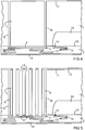
- Figure 4 is a cross section according to Figure 1 for an intermediate product of the method. Elements corresponding to elements shown in Figure 1 are indicated with the same reference numerals.
- Figure 4 shows the substrate 1, the dielectric layer 2 on the main surface 10, the metal layer 3 of the plurality of metal layers 13 embedded in the dielectric layer 2, the contact area 4, the vertical interconnections 14, and the passivation layer 15.
- a trench 18, which surrounds a region of the substrate 1 opposite the contact area 4, is etched into the substrate 1 from the opposite main surface 11. The trench 18 penetrates the substrate 1 and reaches the dielectric layer 2.
- Figure 5 is a cross section according to Figure 4 for a further intermediate product of the method. Elements corresponding to elements shown in Figure 4 are indicated with the same reference numerals.
- the trench 18 is filled with dielectric material, which may be an oxide of the semiconductor material, for instance, to form the insulating layer 8.
- the dielectric material can also be used to form the further dielectric layer 12 on the opposite main surface 11 of the substrate 1.
- the via holes 17 are etched into the substrate 1 until the contact area 4 is exposed in the via holes 17.
- the metallizations 7 are arranged in the via holes 17 to form a plurality of electric contacts on the contact area 4.
- the top metal 5 can be formed in the same method step together with the metallizations 7, or it may be applied as a further metal layer, which is electrically connected to the metallizations 7.
- the remaining voids of the via holes 17 are optionally filled with a filling material 9, especially if the top metal 5 is provided as a separate metal layer continuously covering the interconnection 6.
- the further layers shown in Figure 1 are applied, and thus the device according to Figure 1 is obtained.
- the described structure of the through-substrate via has the advantages that the insulating layer surrounding the plurality of metallizations provides a secure electric insulation from the outer portion of the semiconductor substrate and that cracks of individual metallizations will not entirely interrupt the electric interconnection through the substrate. Moreover, the electrical conductivity of the interconnection is enhanced by the use of a plurality of metallizations.
Landscapes
- Internal Circuitry In Semiconductor Integrated Circuit Devices (AREA)
Abstract
A dielectric layer (2) is arranged on a main surface (10) of a semiconductor substrate (1), a metal layer (3) providing a contact area (4) is embedded in the dielectric layer, a top metal (5) is arranged on an opposite main surface (11) of the substrate, and an electrically conductive interconnection (6) through the substrate, which comprises a plurality of metallizations (7) arranged in a plurality of via holes (17), connects the contact area with the top metal. The plurality of metallizations is surrounded by an insulating layer (8) penetrating the substrate.
Description
- The present invention relates to semiconductor devices comprising a through-substrate via.
- Through-substrate vias, particularly through-silicon vias, are used for electric interconnections between electric conductors that are arranged on opposite surfaces of semiconductor wafers or substrates. The electrically conductive material forming the electric interconnection of such a through-substrate via is usually insulated from the semiconductor material of the substrate by an insulating layer on the sidewall of the via hole. A cleft in the insulating layer may short-circuit the electric interconnection to the semiconductor substrate and thus cause malfunction of the device. If the electrically conductive material is only applied as a thin layer, a crack of the layer may interrupt the electric interconnection.
- It is an object of the present invention to provide a semiconductor device comprising a secure through-substrate via and a method of producing such a semiconductor device.
- This object is achieved with the semiconductor device according to
claim 1 and with the method of producing a semiconductor device according toclaim 5. Embodiments and variants derive from the dependent claims. - The definitions as described above also apply to the following description unless stated otherwise.
- The semiconductor device comprises a substrate of semiconductor material, a dielectric layer on a main surface of the substrate, a metal layer embedded in the dielectric layer, a contact area of the metal layer, a top metal on an opposite main surface of the substrate, and an electrically conductive interconnection through the substrate, the electrically conductive interconnection connecting the contact area with the top metal. The electrically conductive interconnection comprises a plurality of metallizations arranged in a plurality of via holes, and the plurality of metallizations is surrounded by an insulating layer penetrating the substrate.
- In an embodiment of the semiconductor device, the metallizations are electrically interconnected by the top metal.
- In a further embodiment the metallizations are separated from one another by the semiconductor material of the substrate. The metallizations may be in contact with the semiconductor material of the substrate.
- The method of producing such a semiconductor device comprises providing a substrate of semiconductor material with a dielectric layer on a main surface and with a metal layer having a contact area embedded in the dielectric layer, etching a trench into the substrate from an opposite main surface, the trench reaching to the dielectric layer and completely surrounding a region of the substrate, filling the trench with an electrically insulating material, thus forming an insulating layer, etching a plurality of via holes from the opposite main surface to the contact area within the region surrounded by the insulating layer, arranging metallizations in the via holes, each of the metallizations contacting the contact area, and applying a top metal contacting each of the metallizations above the opposite main surface of the substrate.
- In a variant of the method, after arranging the metallizations in the via holes and before applying the top metal, remaining voids in the via holes are filled with a filling material.
- In a further variant of the method, the metallizations are arranged immediately on the semiconductor material of the substrate that is exposed in the via holes.
- In a further variant of the method, a further dielectric layer is arranged on the opposite main surface of the substrate, and the top metal is applied on the further dielectric layer.
- In a further variant of the method, an integrated circuit is formed in the semiconductor material of the substrate, and a plurality of metal layers is formed in the dielectric layer as a wiring of the integrated circuit, the metallizations being connected to the wiring through the contact area.
- In a further variant of the method, the via holes and metallizations are arranged on the contact area at vertices of a square grid.
- The following is a detailed description of examples of the semiconductor device and the method of production in conjunction with the appended figures.
- Figure 1
- is a cross section of a semiconductor device comprising a plurality of metallizations forming an interconnection through the substrate.
- Figure 2
- shows a pattern of the arrangement of the metallizations.
- Figure 3
- shows a further pattern of the arrangement of the metallizations.
- Figure 4
- is a cross section according to
Figure 1 for an intermediate product of the method. - Figure 5
- is a cross section according to
Figure 4 for a further intermediate product comprising via holes. -
Figure 1 is a cross section of a semiconductor device with an electric interconnection through the substrate. Thesubstrate 1 comprises semiconductor material, especially silicon, for instance. Adielectric layer 2 is applied on amain surface 10 of thesubstrate 1. Ametal layer 3 with acontact area 4 is embedded in thedielectric layer 2. Themetal layer 3 may especially be one layer of a plurality ofmetal layers 13, which can be structured and connected byvertical interconnections 14 to form a wiring for an integratedcircuit 19 in thesubstrate 1, in particular a CMOS circuit, for instance. Thedielectric layer 3 may be covered by apassivation layer 15. - A
top metal 5 is applied above the oppositemain surface 11 of thesubstrate 1. Thetop metal 5 can be insulated from the semiconductor material by a furtherdielectric layer 12. Thetop metal 5 and the optional furtherdielectric layer 12 may be covered by afurther passivation layer 16. - An
electric interconnection 6 through the substrate is formed on thecontact area 4. Theinterconnection 6 comprises a plurality ofvia holes 17 in thesubstrate 1 andmetallizations 7, which are arranged in thevia holes 17 in electric contact with thecontact area 4. Aninsulating layer 8, which penetrates thesubstrate 1, surrounds a region including theinterconnection 6 and insulates the plurality ofmetallizations 7 from a portion of thesubstrate 1 that is outside the surrounded region. Theindividual metallizations 7 may be separated from one another by semiconductor material of thesubstrate 1 inside the surrounded region. Theinsulating layer 8 can be formed by atrench 18 in the semiconductor material of thesubstrate 1. Thetrench 18 may be cylindrical, for instance. A dielectric material in thetrench 18 provides the electric insulation. A fillingmaterial 9 may fill remaining voids in thevia holes 17. -
Figure 1 shows that theinsulating layer 8 can be arranged spatially separated from theindividual metallizations 7, which form the electrically conductive part of theinterconnection 6 through the substrate. This is different from conventional through-substrate vias, wherein the electric conductor of the electric interconnection through the substrate is applied immediately on an insulating layer or an insulating region at the sidewall of a via hole. Furthermore, the arrangement of thevia holes 17 and thetrench 18 shown inFigure 1 allows to provide theinterconnection 6 with more than oneindividual metallization 7, so that a plurality of electric conductors can contribute to theinterconnection 6 instead of only a single conductor. -
Figure 2 shows a pattern of the arrangement of the metallizations in the top view that is indicated inFigure 1 by the horizontal broken line and arrows. In the example shown inFigure 2 , each of themetallizations 7 has the shape of a right circular hollow cylinder. The axes of themetallizations 7 are arranged at vertices of a square grid. Themetallizations 7 may instead have other shapes, and their arrangement can differ from the examples shown in the appended figures. The arrangement of themetallizations 7 may especially be irregular. Themetallizations 7 may completely fill thevia holes 17, or remaining voids may be filled with thefilling material 9 shown inFigure 2 . -
Figure 2 shows that theinsulating layer 8, which is also a right circular hollow cylinder in this example, surrounds a cylindrical region of thesubstrate 1 where the plurality ofmetallizations 7 is arranged. Theindividual metallizations 7 are separated from one another by semiconductor material of thesubstrate 1 inside the surrounded region. The horizontal broken line and arrows inFigure 2 indicate the position of the cross section shown inFigure 1 . -
Figure 3 shows a further pattern of the arrangement of the metallizations in the top view that is indicated inFigure 1 by the horizontal broken line and arrows. In the example shown inFigure 3 , themetallizations 7 are also cylindrical and arranged at vertices of a square grid. Themetallizations 7 may completely fill thevia holes 17, or remaining voids may be filled with a fillingmaterial 9. -
Figure 3 shows that, in this example, theinsulating layer 8 comprises flat sections connected by rounded edges in a framelike fashion. It surrounds the region of thesubstrate 1 where the plurality ofmetallizations 7 is arranged. Theindividual metallizations 7 are separated from one another by semiconductor material of thesubstrate 1 inside the surrounded region. The horizontal broken line and arrows inFigure 3 indicate the position of the cross section shown inFigure 1 . -
Figure 4 is a cross section according toFigure 1 for an intermediate product of the method. Elements corresponding to elements shown inFigure 1 are indicated with the same reference numerals.Figure 4 shows thesubstrate 1, thedielectric layer 2 on themain surface 10, themetal layer 3 of the plurality ofmetal layers 13 embedded in thedielectric layer 2, thecontact area 4, thevertical interconnections 14, and thepassivation layer 15. Atrench 18, which surrounds a region of thesubstrate 1 opposite thecontact area 4, is etched into thesubstrate 1 from the oppositemain surface 11. Thetrench 18 penetrates thesubstrate 1 and reaches thedielectric layer 2. -
Figure 5 is a cross section according toFigure 4 for a further intermediate product of the method. Elements corresponding to elements shown inFigure 4 are indicated with the same reference numerals. Thetrench 18 is filled with dielectric material, which may be an oxide of the semiconductor material, for instance, to form the insulatinglayer 8. The dielectric material can also be used to form thefurther dielectric layer 12 on the oppositemain surface 11 of thesubstrate 1. Then the via holes 17 are etched into thesubstrate 1 until thecontact area 4 is exposed in the via holes 17. - The
metallizations 7 are arranged in the via holes 17 to form a plurality of electric contacts on thecontact area 4. Thetop metal 5 can be formed in the same method step together with themetallizations 7, or it may be applied as a further metal layer, which is electrically connected to themetallizations 7. The remaining voids of the via holes 17 are optionally filled with a fillingmaterial 9, especially if thetop metal 5 is provided as a separate metal layer continuously covering theinterconnection 6. The further layers shown inFigure 1 are applied, and thus the device according toFigure 1 is obtained. - The described structure of the through-substrate via has the advantages that the insulating layer surrounding the plurality of metallizations provides a secure electric insulation from the outer portion of the semiconductor substrate and that cracks of individual metallizations will not entirely interrupt the electric interconnection through the substrate. Moreover, the electrical conductivity of the interconnection is enhanced by the use of a plurality of metallizations.
-
- 1
- substrate
- 2
- dielectric layer
- 3
- metal layer
- 4
- contact area
- 5
- top metal
- 6
- interconnection through the substrate
- 7
- metallization
- 8
- insulating layer
- 9
- filling material
- 10
- main surface
- 11
- opposite main surface
- 12
- further dielectric layer
- 13
- plurality of metal layers
- 14
- vertical interconnection
- 15
- passivation layer
- 16
- further passivation layer
- 17
- via hole
- 18
- trench
- 19
- integrated circuit
Claims (10)
- A semiconductor device, comprising:a substrate (1) of semiconductor material,a dielectric layer (2) on a main surface (10) of the substrate (1),a metal layer (3) embedded in the dielectric layer (2),a contact area (4) of the metal layer (3),a top metal (5) on an opposite main surface (11) of the substrate (1), andan electrically conductive interconnection (6) through the substrate (1), the electrically conductive interconnection (6) connecting the contact area (4) with the top metal (5), characterized in thatthe electrically conductive interconnection (6) comprises a plurality of metallizations (7) arranged in a plurality of via holes (17), andthe plurality of metallizations (7) is surrounded by an insulating layer (8) penetrating the substrate (1).
- The semiconductor device according to claim 1, wherein the metallizations (7) of the plurality of metallizations (7) are electrically interconnected by the top metal (5).
- The semiconductor device according to claim 1 or 2, wherein the metallizations (7) of the plurality of metallizations (7) are separated from one another by the semiconductor material of the substrate (1).
- The semiconductor device according to claim 3, wherein the metallizations (7) of the plurality of metallizations (7) are in contact with the semiconductor material of the substrate (1).
- A method of producing a semiconductor device according to one of claims 1 to 4, comprising:providing a substrate (1) of semiconductor material with a dielectric layer (2) on a main surface (10) of the substrate (1), a metal layer (3) embedded in the dielectric layer (2), and a contact area (4) of the metal layer (3),etching a trench (18) into the substrate (1) from an opposite main surface (11) of the substrate (1), the trench (18) reaching to the dielectric layer (2) and completely surrounding a region of the substrate (1),filling the trench (18) with an electrically insulating material, thus forming an insulating layer (8),etching a plurality of via holes (17) from the opposite main surface (11) of the substrate (1) to the contact area (4) within the region surrounded by the insulating layer (8),arranging metallizations (7) in the via holes (17), each of the metallizations (7) contacting the contact area (4), andapplying a top metal (5) contacting each of the metallizations (7) above the opposite main surface (11) of the substrate (1).
- The method according to claim 5, further comprising:after arranging the metallizations (7) in the via holes (17) and before applying the top metal (5), filling remaining voids in the via holes (17) with a filling material (9).
- The method according to claim 5 or 6, wherein the metallizations (7) are arranged immediately on the semiconductor material of the substrate (1) that is exposed in the via holes (17).
- The method according to one of claims 5 to 7, further comprising:arranging a further dielectric layer (12) on the opposite main surface (11) of the substrate (1), andapplying the top metal (5) on the further dielectric layer (12).
- The method according to one of claims 5 to 8, further comprising:forming an integrated circuit (19) in the semiconductor material of the substrate (1), andforming a plurality of metal layers (13) in the dielectric layer (2) as a wiring of the integrated circuit (19), the metallizations (7) being connected to the wiring through the contact area (4).
- The method according to one of claims 5 to 9, wherein the via holes (17) and metallizations (7) are arranged on the contact area (4) at vertices of a square grid.
Priority Applications (5)
| Application Number | Priority Date | Filing Date | Title |
|---|---|---|---|
| EP18157371.8A EP3528281A1 (en) | 2018-02-19 | 2018-02-19 | Semiconductor device with through-substrate via and its method of manufacture |
| US16/968,815 US11404352B2 (en) | 2018-02-19 | 2019-02-15 | Semiconductor device with through-substrate via and its method of manufacture |
| PCT/EP2019/053847 WO2019158706A1 (en) | 2018-02-19 | 2019-02-15 | Semiconductor device with through-substrate via and its method of manufacture |
| EP19705355.6A EP3756216B1 (en) | 2018-02-19 | 2019-02-15 | METHOD FOR PRODUCING A SUBSTATE-CONTACTING SEMICONDUCTOR ELEMENT |
| CN201980011331.6A CN112005365B (en) | 2018-02-19 | 2019-02-15 | Methods of manufacturing semiconductor devices |
Applications Claiming Priority (1)
| Application Number | Priority Date | Filing Date | Title |
|---|---|---|---|
| EP18157371.8A EP3528281A1 (en) | 2018-02-19 | 2018-02-19 | Semiconductor device with through-substrate via and its method of manufacture |
Publications (1)
| Publication Number | Publication Date |
|---|---|
| EP3528281A1 true EP3528281A1 (en) | 2019-08-21 |
Family
ID=61249511
Family Applications (2)
| Application Number | Title | Priority Date | Filing Date |
|---|---|---|---|
| EP18157371.8A Withdrawn EP3528281A1 (en) | 2018-02-19 | 2018-02-19 | Semiconductor device with through-substrate via and its method of manufacture |
| EP19705355.6A Active EP3756216B1 (en) | 2018-02-19 | 2019-02-15 | METHOD FOR PRODUCING A SUBSTATE-CONTACTING SEMICONDUCTOR ELEMENT |
Family Applications After (1)
| Application Number | Title | Priority Date | Filing Date |
|---|---|---|---|
| EP19705355.6A Active EP3756216B1 (en) | 2018-02-19 | 2019-02-15 | METHOD FOR PRODUCING A SUBSTATE-CONTACTING SEMICONDUCTOR ELEMENT |
Country Status (4)
| Country | Link |
|---|---|
| US (1) | US11404352B2 (en) |
| EP (2) | EP3528281A1 (en) |
| CN (1) | CN112005365B (en) |
| WO (1) | WO2019158706A1 (en) |
Families Citing this family (1)
| Publication number | Priority date | Publication date | Assignee | Title |
|---|---|---|---|---|
| KR20240120450A (en) * | 2023-01-31 | 2024-08-07 | 에스케이하이닉스 주식회사 | Semiconductor device with through vias of various shapes and method for manufacturing the same |
Citations (5)
| Publication number | Priority date | Publication date | Assignee | Title |
|---|---|---|---|---|
| WO2007024009A1 (en) * | 2005-08-26 | 2007-03-01 | Honda Motor Co., Ltd. | Semiconductor integrated circuit device and method for manufacturing same |
| WO2009050207A1 (en) * | 2007-10-15 | 2009-04-23 | Interuniversitair Microelectronica Centrum Vzw | Method for producing electrical interconnects and devices made thereof |
| US20130321680A1 (en) * | 2012-05-31 | 2013-12-05 | Canon Kabushiki Kaisha | Manufacturing method for semiconductor device and semiconductor device |
| US20140054743A1 (en) * | 2012-08-24 | 2014-02-27 | Newport Fab, Llc Dba Jazz Semiconductor | Isolated Through Silicon Vias in RF Technologies |
| WO2015185354A2 (en) * | 2014-06-06 | 2015-12-10 | Robert Bosch Gmbh | Semiconductor component having at least one via in the carrier substrate and method for producing such a via |
Family Cites Families (4)
| Publication number | Priority date | Publication date | Assignee | Title |
|---|---|---|---|---|
| DE102013208816A1 (en) * | 2013-05-14 | 2014-11-20 | Robert Bosch Gmbh | A method of creating a via in a CMOS substrate |
| US9401323B1 (en) | 2015-04-03 | 2016-07-26 | International Business Machines Corporation | Protected through semiconductor via (TSV) |
| US9786618B2 (en) * | 2015-11-16 | 2017-10-10 | Taiwan Semiconductor Manufacturing Company Ltd. | Semiconductor structure and manufacturing method thereof |
| US10504821B2 (en) | 2016-01-29 | 2019-12-10 | United Microelectronics Corp. | Through-silicon via structure |
-
2018
- 2018-02-19 EP EP18157371.8A patent/EP3528281A1/en not_active Withdrawn
-
2019
- 2019-02-15 WO PCT/EP2019/053847 patent/WO2019158706A1/en not_active Ceased
- 2019-02-15 CN CN201980011331.6A patent/CN112005365B/en active Active
- 2019-02-15 EP EP19705355.6A patent/EP3756216B1/en active Active
- 2019-02-15 US US16/968,815 patent/US11404352B2/en active Active
Patent Citations (5)
| Publication number | Priority date | Publication date | Assignee | Title |
|---|---|---|---|---|
| WO2007024009A1 (en) * | 2005-08-26 | 2007-03-01 | Honda Motor Co., Ltd. | Semiconductor integrated circuit device and method for manufacturing same |
| WO2009050207A1 (en) * | 2007-10-15 | 2009-04-23 | Interuniversitair Microelectronica Centrum Vzw | Method for producing electrical interconnects and devices made thereof |
| US20130321680A1 (en) * | 2012-05-31 | 2013-12-05 | Canon Kabushiki Kaisha | Manufacturing method for semiconductor device and semiconductor device |
| US20140054743A1 (en) * | 2012-08-24 | 2014-02-27 | Newport Fab, Llc Dba Jazz Semiconductor | Isolated Through Silicon Vias in RF Technologies |
| WO2015185354A2 (en) * | 2014-06-06 | 2015-12-10 | Robert Bosch Gmbh | Semiconductor component having at least one via in the carrier substrate and method for producing such a via |
Also Published As
| Publication number | Publication date |
|---|---|
| US20210005534A1 (en) | 2021-01-07 |
| WO2019158706A1 (en) | 2019-08-22 |
| CN112005365A (en) | 2020-11-27 |
| US11404352B2 (en) | 2022-08-02 |
| EP3756216B1 (en) | 2026-05-20 |
| EP3756216A1 (en) | 2020-12-30 |
| CN112005365B (en) | 2024-03-01 |
Similar Documents
| Publication | Publication Date | Title |
|---|---|---|
| US8415807B2 (en) | Semiconductor structure and method for making the same | |
| US9831140B2 (en) | Wafer having pad structure | |
| KR20100045836A (en) | A semiconductor wafer and a semiconductor devices including merged guard ring patterns and a process monitoring pattern | |
| US8679937B2 (en) | Method for fabricating a capacitor and capacitor structure thereof | |
| US10559543B2 (en) | Semiconductor device having a protection trench, semiconductor wafer including the same, and semiconductor package | |
| EP2597677B1 (en) | Semiconductor device with through-substrate via covered by a solder ball and related method of production | |
| EP2620978B1 (en) | Semiconductor device with internal substrate contact and method of production | |
| CN109390353A (en) | Semiconductor element and manufacturing method thereof | |
| US8237288B1 (en) | Enhanced electromigration resistance in TSV structure and design | |
| US11404352B2 (en) | Semiconductor device with through-substrate via and its method of manufacture | |
| TWI643304B (en) | Bauelement mit durchkontaktierung und verfahren zur herstellungcomponent with through-contact and process for its production | |
| CN105489581B (en) | Semiconductor structure and preparation method thereof | |
| CN110301044B (en) | Semiconductor device with a semiconductor layer having a plurality of semiconductor layers | |
| JP2004014573A5 (en) | ||
| CN113437042B (en) | Pad structure, semiconductor test structure and semiconductor test method | |
| US10276493B2 (en) | Semiconductor structure and method for fabricating the same | |
| EP2648214B1 (en) | Methods of producing a semiconductor device with a through-substrate via | |
| US7485926B2 (en) | SOI contact structures | |
| US10796947B2 (en) | Method of manufacturing a semiconductor device | |
| EP3564994B1 (en) | Semiconductor device with through-substrate via | |
| EP2790211A1 (en) | Method of producing a through-substrate via in a semiconductor device and semiconductor device comprising a through-substrate via | |
| CN115332258B (en) | A semiconductor structure and a method for manufacturing the same | |
| CN114784486B (en) | Electromagnetic shielding packaging structure and manufacturing method thereof | |
| CN118471932B (en) | Semiconductor device and method for manufacturing the same | |
| US6884662B1 (en) | Enhanced adhesion strength between mold resin and polyimide |
Legal Events
| Date | Code | Title | Description |
|---|---|---|---|
| PUAI | Public reference made under article 153(3) epc to a published international application that has entered the european phase |
Free format text: ORIGINAL CODE: 0009012 |
|
| AK | Designated contracting states |
Kind code of ref document: A1 Designated state(s): AL AT BE BG CH CY CZ DE DK EE ES FI FR GB GR HR HU IE IS IT LI LT LU LV MC MK MT NL NO PL PT RO RS SE SI SK SM TR |
|
| AX | Request for extension of the european patent |
Extension state: BA ME |
|
| STAA | Information on the status of an ep patent application or granted ep patent |
Free format text: STATUS: THE APPLICATION IS DEEMED TO BE WITHDRAWN |
|
| 18D | Application deemed to be withdrawn |
Effective date: 20200222 |