EP3528277A2 - System and method of preparing integrated circuits for backside probing using charged particle beams - Google Patents
System and method of preparing integrated circuits for backside probing using charged particle beams Download PDFInfo
- Publication number
- EP3528277A2 EP3528277A2 EP19153236.5A EP19153236A EP3528277A2 EP 3528277 A2 EP3528277 A2 EP 3528277A2 EP 19153236 A EP19153236 A EP 19153236A EP 3528277 A2 EP3528277 A2 EP 3528277A2
- Authority
- EP
- European Patent Office
- Prior art keywords
- milling
- active layer
- reached
- thin layer
- backside
- Prior art date
- Legal status (The legal status is an assumption and is not a legal conclusion. Google has not performed a legal analysis and makes no representation as to the accuracy of the status listed.)
- Pending
Links
Images



Classifications
-
- G—PHYSICS
- G01—MEASURING; TESTING
- G01R—MEASURING ELECTRIC VARIABLES; MEASURING MAGNETIC VARIABLES
- G01R31/00—Arrangements for testing electric properties; Arrangements for locating electric faults; Arrangements for electrical testing characterised by what is being tested not provided for elsewhere
- G01R31/26—Testing of individual semiconductor devices
- G01R31/2644—Adaptations of individual semiconductor devices to facilitate the testing thereof
-
- H—ELECTRICITY
- H01—ELECTRIC ELEMENTS
- H01J—ELECTRIC DISCHARGE TUBES OR DISCHARGE LAMPS
- H01J37/00—Discharge tubes with provision for introducing objects or material to be exposed to the discharge, e.g. for the purpose of examination or processing thereof
- H01J37/30—Electron-beam or ion-beam tubes for localised treatment of objects
- H01J37/302—Controlling tubes by external information, e.g. program control
-
- H—ELECTRICITY
- H10—SEMICONDUCTOR DEVICES; ELECTRIC SOLID-STATE DEVICES NOT OTHERWISE PROVIDED FOR
- H10P—GENERIC PROCESSES OR APPARATUS FOR THE MANUFACTURE OR TREATMENT OF DEVICES COVERED BY CLASS H10
- H10P74/00—Testing or measuring during manufacture or treatment of wafers, substrates or devices
- H10P74/20—Testing or measuring during manufacture or treatment of wafers, substrates or devices characterised by the properties tested or measured, e.g. structural or electrical properties
- H10P74/203—Structural properties, e.g. testing or measuring thicknesses, line widths, warpage, bond strengths or physical defects
-
- H—ELECTRICITY
- H01—ELECTRIC ELEMENTS
- H01J—ELECTRIC DISCHARGE TUBES OR DISCHARGE LAMPS
- H01J37/00—Discharge tubes with provision for introducing objects or material to be exposed to the discharge, e.g. for the purpose of examination or processing thereof
- H01J37/30—Electron-beam or ion-beam tubes for localised treatment of objects
- H01J37/304—Controlling tubes by information coming from the objects or from the beam, e.g. correction signals
-
- G—PHYSICS
- G01—MEASURING; TESTING
- G01N—INVESTIGATING OR ANALYSING MATERIALS BY DETERMINING THEIR CHEMICAL OR PHYSICAL PROPERTIES
- G01N23/00—Investigating or analysing materials by the use of wave or particle radiation, e.g. X-rays or neutrons, not covered by groups G01N3/00 – G01N17/00, G01N21/00 or G01N22/00
- G01N23/22—Investigating or analysing materials by the use of wave or particle radiation, e.g. X-rays or neutrons, not covered by groups G01N3/00 – G01N17/00, G01N21/00 or G01N22/00 by measuring secondary emission from the material
- G01N23/225—Investigating or analysing materials by the use of wave or particle radiation, e.g. X-rays or neutrons, not covered by groups G01N3/00 – G01N17/00, G01N21/00 or G01N22/00 by measuring secondary emission from the material using electron or ion
- G01N23/2255—Investigating or analysing materials by the use of wave or particle radiation, e.g. X-rays or neutrons, not covered by groups G01N3/00 – G01N17/00, G01N21/00 or G01N22/00 by measuring secondary emission from the material using electron or ion using incident ion beams, e.g. proton beams
- G01N23/2257—Measuring excited X-rays, i.e. particle-induced X-ray emission [PIXE]
-
- G—PHYSICS
- G01—MEASURING; TESTING
- G01R—MEASURING ELECTRIC VARIABLES; MEASURING MAGNETIC VARIABLES
- G01R31/00—Arrangements for testing electric properties; Arrangements for locating electric faults; Arrangements for electrical testing characterised by what is being tested not provided for elsewhere
- G01R31/26—Testing of individual semiconductor devices
-
- G—PHYSICS
- G01—MEASURING; TESTING
- G01R—MEASURING ELECTRIC VARIABLES; MEASURING MAGNETIC VARIABLES
- G01R31/00—Arrangements for testing electric properties; Arrangements for locating electric faults; Arrangements for electrical testing characterised by what is being tested not provided for elsewhere
- G01R31/26—Testing of individual semiconductor devices
- G01R31/265—Contactless testing
-
- G—PHYSICS
- G01—MEASURING; TESTING
- G01R—MEASURING ELECTRIC VARIABLES; MEASURING MAGNETIC VARIABLES
- G01R31/00—Arrangements for testing electric properties; Arrangements for locating electric faults; Arrangements for electrical testing characterised by what is being tested not provided for elsewhere
- G01R31/26—Testing of individual semiconductor devices
- G01R31/265—Contactless testing
- G01R31/2653—Contactless testing using electron beams
-
- G—PHYSICS
- G01—MEASURING; TESTING
- G01R—MEASURING ELECTRIC VARIABLES; MEASURING MAGNETIC VARIABLES
- G01R31/00—Arrangements for testing electric properties; Arrangements for locating electric faults; Arrangements for electrical testing characterised by what is being tested not provided for elsewhere
- G01R31/26—Testing of individual semiconductor devices
- G01R31/27—Testing of devices without physical removal from the circuit of which they form part, e.g. compensating for effects surrounding elements
-
- G—PHYSICS
- G01—MEASURING; TESTING
- G01R—MEASURING ELECTRIC VARIABLES; MEASURING MAGNETIC VARIABLES
- G01R31/00—Arrangements for testing electric properties; Arrangements for locating electric faults; Arrangements for electrical testing characterised by what is being tested not provided for elsewhere
- G01R31/26—Testing of individual semiconductor devices
- G01R31/27—Testing of devices without physical removal from the circuit of which they form part, e.g. compensating for effects surrounding elements
- G01R31/275—Testing of devices without physical removal from the circuit of which they form part, e.g. compensating for effects surrounding elements for testing individual semiconductor components within integrated circuits
-
- G—PHYSICS
- G01—MEASURING; TESTING
- G01R—MEASURING ELECTRIC VARIABLES; MEASURING MAGNETIC VARIABLES
- G01R31/00—Arrangements for testing electric properties; Arrangements for locating electric faults; Arrangements for electrical testing characterised by what is being tested not provided for elsewhere
- G01R31/28—Testing of electronic circuits, e.g. by signal tracer
-
- G—PHYSICS
- G01—MEASURING; TESTING
- G01R—MEASURING ELECTRIC VARIABLES; MEASURING MAGNETIC VARIABLES
- G01R31/00—Arrangements for testing electric properties; Arrangements for locating electric faults; Arrangements for electrical testing characterised by what is being tested not provided for elsewhere
- G01R31/28—Testing of electronic circuits, e.g. by signal tracer
- G01R31/2851—Testing of integrated circuits [IC]
- G01R31/2898—Sample preparation, e.g. removing encapsulation, etching
-
- G—PHYSICS
- G01—MEASURING; TESTING
- G01R—MEASURING ELECTRIC VARIABLES; MEASURING MAGNETIC VARIABLES
- G01R31/00—Arrangements for testing electric properties; Arrangements for locating electric faults; Arrangements for electrical testing characterised by what is being tested not provided for elsewhere
- G01R31/28—Testing of electronic circuits, e.g. by signal tracer
- G01R31/302—Contactless testing
- G01R31/305—Contactless testing using electron beams
- G01R31/307—Contactless testing using electron beams of integrated circuits
-
- H—ELECTRICITY
- H01—ELECTRIC ELEMENTS
- H01J—ELECTRIC DISCHARGE TUBES OR DISCHARGE LAMPS
- H01J37/00—Discharge tubes with provision for introducing objects or material to be exposed to the discharge, e.g. for the purpose of examination or processing thereof
- H01J37/26—Electron or ion microscopes; Electron or ion diffraction tubes
- H01J37/266—Measurement of magnetic or electric fields in the object; Lorentzmicroscopy
-
- H—ELECTRICITY
- H01—ELECTRIC ELEMENTS
- H01J—ELECTRIC DISCHARGE TUBES OR DISCHARGE LAMPS
- H01J37/00—Discharge tubes with provision for introducing objects or material to be exposed to the discharge, e.g. for the purpose of examination or processing thereof
- H01J37/30—Electron-beam or ion-beam tubes for localised treatment of objects
- H01J37/305—Electron-beam or ion-beam tubes for localised treatment of objects for casting, melting, evaporating, or etching
-
- H—ELECTRICITY
- H01—ELECTRIC ELEMENTS
- H01J—ELECTRIC DISCHARGE TUBES OR DISCHARGE LAMPS
- H01J37/00—Discharge tubes with provision for introducing objects or material to be exposed to the discharge, e.g. for the purpose of examination or processing thereof
- H01J37/30—Electron-beam or ion-beam tubes for localised treatment of objects
- H01J37/305—Electron-beam or ion-beam tubes for localised treatment of objects for casting, melting, evaporating, or etching
- H01J37/3053—Electron-beam or ion-beam tubes for localised treatment of objects for casting, melting, evaporating, or etching for evaporating or etching
- H01J37/3056—Electron-beam or ion-beam tubes for localised treatment of objects for casting, melting, evaporating, or etching for evaporating or etching for microworking, e. g. etching of gratings or trimming of electrical components
-
- H—ELECTRICITY
- H10—SEMICONDUCTOR DEVICES; ELECTRIC SOLID-STATE DEVICES NOT OTHERWISE PROVIDED FOR
- H10P—GENERIC PROCESSES OR APPARATUS FOR THE MANUFACTURE OR TREATMENT OF DEVICES COVERED BY CLASS H10
- H10P74/00—Testing or measuring during manufacture or treatment of wafers, substrates or devices
- H10P74/20—Testing or measuring during manufacture or treatment of wafers, substrates or devices characterised by the properties tested or measured, e.g. structural or electrical properties
- H10P74/207—Electrical properties, e.g. testing or measuring of resistance, deep levels or capacitance-voltage characteristics
-
- H—ELECTRICITY
- H10—SEMICONDUCTOR DEVICES; ELECTRIC SOLID-STATE DEVICES NOT OTHERWISE PROVIDED FOR
- H10P—GENERIC PROCESSES OR APPARATUS FOR THE MANUFACTURE OR TREATMENT OF DEVICES COVERED BY CLASS H10
- H10P74/00—Testing or measuring during manufacture or treatment of wafers, substrates or devices
- H10P74/23—Testing or measuring during manufacture or treatment of wafers, substrates or devices characterised by multiple measurements, corrections, marking or sorting processes
- H10P74/238—Testing or measuring during manufacture or treatment of wafers, substrates or devices characterised by multiple measurements, corrections, marking or sorting processes comprising acting in response to an ongoing measurement without interruption of processing, e.g. endpoint detection or in-situ thickness measurement
-
- H—ELECTRICITY
- H01—ELECTRIC ELEMENTS
- H01J—ELECTRIC DISCHARGE TUBES OR DISCHARGE LAMPS
- H01J2237/00—Discharge tubes exposing object to beam, e.g. for analysis treatment, etching, imaging
- H01J2237/30—Electron or ion beam tubes for processing objects
- H01J2237/304—Controlling tubes
- H01J2237/30433—System calibration
- H01J2237/30438—Registration
-
- H—ELECTRICITY
- H01—ELECTRIC ELEMENTS
- H01J—ELECTRIC DISCHARGE TUBES OR DISCHARGE LAMPS
- H01J2237/00—Discharge tubes exposing object to beam, e.g. for analysis treatment, etching, imaging
- H01J2237/30—Electron or ion beam tubes for processing objects
- H01J2237/304—Controlling tubes
- H01J2237/30466—Detecting endpoint of process
-
- H—ELECTRICITY
- H01—ELECTRIC ELEMENTS
- H01J—ELECTRIC DISCHARGE TUBES OR DISCHARGE LAMPS
- H01J2237/00—Discharge tubes exposing object to beam, e.g. for analysis treatment, etching, imaging
- H01J2237/30—Electron or ion beam tubes for processing objects
- H01J2237/317—Processing objects on a microscale
- H01J2237/31749—Focused ion beam
-
- H—ELECTRICITY
- H01—ELECTRIC ELEMENTS
- H01J—ELECTRIC DISCHARGE TUBES OR DISCHARGE LAMPS
- H01J37/00—Discharge tubes with provision for introducing objects or material to be exposed to the discharge, e.g. for the purpose of examination or processing thereof
- H01J37/02—Details
- H01J37/22—Optical, image processing or photographic arrangements associated with the tube
- H01J37/226—Optical arrangements for illuminating the object; optical arrangements for collecting light from the object
-
- H—ELECTRICITY
- H01—ELECTRIC ELEMENTS
- H01J—ELECTRIC DISCHARGE TUBES OR DISCHARGE LAMPS
- H01J49/00—Particle spectrometers or separator tubes
- H01J49/02—Details
- H01J49/10—Ion sources; Ion guns
- H01J49/14—Ion sources; Ion guns using particle bombardment, e.g. ionisation chambers
Definitions
- This invention relates to the diagnosis and characterization of electrically active integrated circuits using charged particle beams, and to the probing of electrical activity from the backside of modern integrated circuitry while they are being electrically stimulated by a testing means. More specifically, the invention describes a system and method for preparing modern finFET integrated circuits to enable electron-beam waveform probing.
- Integrated Circuits undergo electrical device characterization throughout their design and manufacturing life cycle to verify that the ICs are meeting their performance expectations.
- An IC not meeting design performance expectations may undergo a debugging and failure analysis process to determine the root cause of its non-conformance.
- the field of electrical failure analysis involves the diagnosis and characterization of electrically active IC devices for the purpose of identifying the root cause of such non-conformances.
- values, procedures, or apparatus' are referred to as “lowest”, “best”, “minimum,” or the like. It will be appreciated that such descriptions are intended to indicate that a selection among many used functional alternatives can be made, and such selections need not be better, smaller, or otherwise preferable to other selections.
- optical lasers focused on individual transistors within an IC to measure electrical activity within an active IC. See for example Kindereit, Ulrike, "Fundamentals and Future Applications of Laser Voltage Probing", IEEE Reliability Physics Symposium, pp. 1-11, Jun. 2014 .
- a limitation of optical probing techniques is that they are unable to resolve features substantially smaller than the wavelength of the light used in the optical probe, and despite a recent push to shorten the wavelength and use visible optical probing techniques (see, for example, U. S. Patent 9,651,610 B2 ), the feature sizes of advanced ICs have now shrunk well beyond the limit that optical diagnostic tools can resolve.
- a renewed interest therefore exists for diagnostic tools that derive their imaging resolution from charged particle beams that can resolve features much smaller than optical wavelengths.
- U. S. Patent 4,706,019 filed in 1985 discloses an electron beam test probe system for analyzing ICs from their front side.
- advanced ICs became packaged in a "flip-chip" state where access to the front active side of an active IC was no longer possible, and this advance in packaging led to a need to probe ICs from their back substrate side.
- U. S. Patent 5,972,725 (hereafter '725) discloses a method of precisely measuring electrical parameters from the back substrate side of an IC by using a scanning electron microscope probe directed at active regions of the IC exposed by the removal of the semiconductor substrate.
- Patent 6.872,581 discloses a method of probing active ICs from their back substrate side using charged particle beams - electron or ion beams - directed at a thinned substrate layer where electrical activity beneath the thinned substrate layer induces an electrical potential on the outer surface that is probed by the charged particle beam.
- '725 teaches a method of using a scanning electron microscope to measure electrical activity from the backside of an IC by thinning the substrate all the way to the active regions of the IC, while '581 allows that either an electron or an ion microscope can probe electrical activity from a surface near, but not at, the active regions of the IC.
- a typical tri-gate transistor in an advanced IC will consist of a fin of silicon that is of order ten nanometers wide, fifty nanometers tall, and having a gate that is of order ten or fewer nanometers long.
- electrical activity within active silicon resides within the topmost fifty nanometers of the IC substrate.
- the substrate material needs to be removed to expose the bottom side of the fins of silicon that comprise the active transistors of the IC.
- the '725 patent envisioned removing the bulk substrate to a region approximately one micron from the front side of the IC, while the '581 method envisioned removing the bulk substrate to within one to three microns.
- the substrate With modern tri-gate transistors, however, the substrate must be removed to within approximately fifty nanometers of the front side of the IC, with a tolerance of only ten or twenty nanometers, and such sample preparation presents a challenge that was not anticipated by the '581 and '725 patents. If too little substrate material is removed, the individual transistor fins are not exposed and cannot be electrically exposed, yet if too much substrate material is removed, the transistor fins themselves will be removed, thereby preventing their electrical characterization.
- a conventional IC may be patterned and built on the front side of a silicon substrate, with the substrate being approximately 760 microns thick.
- the active circuitry comprises fin-shaped tri-gate transistors that reside within approximately fifty nanometers of the silicon surface. Processes are disclosed for the removal of nearly the entirety of this substrate material so that in the end only the active transistors remain and the IC remains electrically functional.
- ICs are tested by attaching them to a printed circuit board known as a load board.
- the load board typically connects to an automated electrical tester that powers the IC and supplies electrical test signals, and, in some embodiments, the load board will form a sliding vacuum seal required to both position the device under test (DUT) relative to the charged-particle beams, and to maintain needed vacuum integrity within the microscope.
- DUT device under test
- the load board will form a sliding vacuum seal required to both position the device under test (DUT) relative to the charged-particle beams, and to maintain needed vacuum integrity within the microscope.
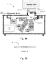
- FIG. 1A is an example charged particle beam system 100 in accordance with an embodiment of the present disclosure.
- the system 100 may be a dual-beam system, as known in the art.
- the system 100 may include both an electron beam column and an ion beam column.
- the column labeled SEM may include an electron emitter, such as a Schottky emitter, various lenses for focusing the electron beam, and detectors.
- the detectors may be used to detect backscattered and secondary electrons, for example, but other photon-centric detectors may also be included, such as ultraviolet, visible, and infrared light detectors and/or x-ray detectors.
- the ion beam column labeled as such in Figure 1A , includes an ion source, such as a plasma or liquid metal ion source, along with focusing optics for shaping the ion beam.
- ion source such as a plasma or liquid metal ion source
- the detectors discussed above in relation with the SEM column may also be used in conjunction with the ion beam column. For example, secondary electrons and/or secondary ions may be detected when the sample is subject to an ion beam.
- the system 100 further includes an infrared imaging system for locating regions of interest in the active area of the sample 102.
- the regions of interest are areas where one or more transistors, e.g., finFETs, are to be analyzed. Locating the one or more transistors helps the system 100 navigate to the area that requires additional processing to expose the regions of interest.
- the infrared imaging system at least includes a retractable mirror and an infrared camera, labeled IR in Figure 1A . Additionally (and not shown), the infrared imaging system includes a suitable IR source for projecting IR light through a sample and towards the retractable mirror.
- the system 100 also includes an electrical tester that can be coupled to an IC under test (e.g., sample 102), which may also be referred to as a device under test (DUT).
- the electrical tester may provide clock and/or data signals to one or more functional blocks of the IC device to drive the transistors of the functional block.
- One or more of the transistors of a designated area, e.g., region of interest, may desirably be examined for failure mechanisms, and which may be excavated by ion milling, for example, for specific testing. The excavation of the transistors may be performed as disclosed herein.
- the system 100 also includes other ancillary equipment for producing a low pressure environment required for operating the ion beam and SEM columns.
- a vacuum seal may seal the sample 102 and electrical tester to the SEM column, ion beam column, and infrared imaging system.
- the system 100 includes a turbo pump, and one or more ion pumps, all coupled to the vacuum chamber.
- a stage may be included in the vacuum chamber to manipulate the location of the ion beam and SEM columns, the sample 102, or both. The stage may be moved in at least three degrees of freedom, but additional degrees may also be included allowing for both translational and rotational movement.
- the system 100 includes a controller coupled to the ion beam column, the SEM column, the detectors, the infrared imaging system, the electrical tester, and the vacuum pumps.
- the controller is coupled to control operation of the various components for implementing the techniques disclosed herein.
- the method 200 may use the SEM, detectors, and ion beam columns along with the infrared imaging system to prepare the sample 102 for electrical testing.
- the method 200 may include locating a desired probe location, milling substrate material to uncover the probe location, and end point detection to determine when a transistor to test has been uncovered.
- the end point detection may be sensitive enough to remove oxide material without detrimentally affecting the transistor regions so that electrical testing may occur while physical probing of the transistor occurs, such as with optical or electron beam techniques.
- the sample 102 which may be thermally managed, is coupled to a load board.
- the load board is coupled to the electrical tester, and the sample 102.
- the load board relays electrical test signals from the electrical tester to the sample 102.
- Figure 1A shows an example location for the load board.
- the load board may be on the bottom side of the sample 102.
- the load board may be used for coupling the vacuum chamber to the electrical tester and may include at least two dimensional alignment mechanics.
- the load board may include heat sinking and heat exchange aspects to remove heat from the sample 102.
- the load board may include a fluid heat exchanger or a thick copper plane, but other techniques may also be implemented.
- FIG. 1B is an example IC 102 in accordance with an embodiment of the present disclosure.
- the IC 102 which may also be simply referred to as sample 102, includes a substrate 120 and an active area 130.
- the substrate 120 may be formed from any known semiconductor material, such as silicon, GaAs, InP, Ge, GaN, etc. While silicon is used to illustrate the disclosure, the disclosure is not limited as such.
- the active area 130 may include one or more levels of active circuitry, such as transistors coupled by metal traces. In some examples, the transistors are finFETs, as discussed herein. However, while the disclosed processing techniques may be advantageous for finFET processing, the techniques are not limited by the transistor technology. As used herein, a backside of the sample 102 is the substrate side whereas a front side of the sample 102 is the active area 130 side.
- Figure 2A is a flow chart of an example method 200 in accordance with an embodiment of the present disclosure.
- the method 200 may be implemented on the system 100, for example, to at least partially prepare and locate a desired transistor, circuit(s), electrical trace, or combinations thereof, of a sample or IC, such as the sample 102, to undergo electrical testing. While some of the preparation steps may be performed in the example system 100, other steps may be performed outside of and prior to loading an IC into the system 100. For example, bulk removal of substrate material may be performed prior to loading the sample into the system 100. While not all examples of sample preparations, e.g., material removal and end point detection, are explicitly covered herein, they are within the bounds of the present disclosure and fully contemplated.
- the method 200 may begin at step 201, which includes the bulk removal of substrate material from a back side of an IC or sample.
- the IC or sample may be formed in or from silicon, GaAs, InP, Ge, or any semiconductor material. While silicon may be used as an illustrative example in the disclosure, the disclosure should not be considered so limited.
- the bulk removal may be implemented using one or more mechanical techniques, such as lapping, milling, polishing, or may be implemented using other techniques commonly used to thin semiconductor substrates, such as laser ablation, chemical etching, etc. In some embodiments, a combination of techniques may be used to remove the bulk substrate material. Also known to those skilled in the art of preparing samples are tools for accurately measuring residual substrate thickness after the milling process.
- the substrate need not be thinned over the entire region of the IC, and the thinning may be confined to an area above a region of interest, e.g., a desired probing region in an active area disposed on an opposite side of the IC.
- a small pocket can be formed within the IC substrate using one or more mechanical milling techniques.
- the bulk removal of the substrate may include removal of substrate across an entire backside of an IC or sample. In other embodiments, the bulk removal may be performed in a small area on the backside above a desired probe area, e.g., a region of interest.
- the step 201 may be followed by the step 203, which includes polishing the backside of the IC or sample.
- the polishing may be performed using any known method for wafer material polishing, such as using a slurry and polishing pad.
- thinning an IC or sample to approximately 20 microns residual thickness of substrate material using a mechanical technique then removing another 10 microns in a polishing process that progressively uses finer polishing compounds results in an IC with approximately ten microns of residual silicon substrate having an optically smooth sub-micron surface roughness.
- the optically smooth sub-micron surface roughness may be desirable to reduce or eliminate uneven exposure of the active transistor fins post a subsequent thinning step, such as a plasma-based thinning process.
- a subsequent thinning step such as a plasma-based thinning process.
- the residual silicon is substantially thicker than ten microns after polishing (e.g., 15 microns or more residual thickness)
- the subsequent thinning process may require excessive time to complete.
- the residual silicon after polishing is substantially thinner than ten microns (e.g., 5 microns or less)
- the subsequent thinning process may not eliminate the surface roughness left after the mechanical polishing process and will lead to uneven exposure of the active transistor fins.
- the step 203 may optionally be followed by step 205, which includes electrically testing the IC or sample to confirm device functionality.
- the IC device can be inserted into a charged particle beam system (step 207).
- the charged particle system such as the system 100, may include a scanning electron microscope for imaging and electrically probing nanometer features on the IC, a focused ion beam tool capable of imaging and removing the residual substrate material to the level of the fin transistors, and an infrared imaging system capable of looking through silicon substrate material to see features that have been patterned onto the IC during its manufacture.
- the charged particle system may omit the infrared imaging system.
- the step 207 may be followed by the step 209, which includes locating corner fiducials that have been patterned onto the IC surface during its manufacture.
- the corner fiducials may be observed by looking through the silicon substrate using the infrared camera, which may allow the corner fiducials, which are on the front side, be located.
- the infrared camera must have an infrared illumination source to illuminate the IC for inspection.
- the infrared camera is used to determine and calibrate an offset between the known corner fiducials that are visible beneath the substrate, e.g., on the front side, and other fiducials, such as chip corners, that can be observed using electron and ion beam imaging, neither of which can image through the remaining substrate material and image the corner fiducials on the front side of the IC.
- Step 209 may be followed by the step 211, which includes calibrate offsets to determine between fiducial features observable by electron and ion beam imaging and fiducial features observable through the substrate using infrared imaging.
- calibrated offsets have been determined, see Figures 3A through 3C for detail, between fiducial features observable by electron and ion beam imaging, and fiducial features observed through the substrate using the infrared imager, a mechanical stage system can move to any location on the IC.
- a debug technique will specify a region of the IC to be probed, and the coordinates of that region will be known.
- the region of the IC to be probed could be an individual transistor, a small circuit comprised of several transistors, a region containing many circuits, or even a metal trace of the IC.
- mechanical stages can move the IC to position the known probe location in an optimal location to be acted upon by the focused ion beam tool.
- the step 211 may be followed by the step 213, which includes navigating to a region outside of the probe location, e.g., the region of interest, and milling an alignment fiducial marker on the backside surface of the IC.
- the alignment fiducial may reduce or eliminate possible navigation errors by helping more accurately determine where the probe location and final milling should be performed.
- the milling of the alignment fiducial may be performed using a focused ion beam tool, which may be a plasma-based ion mill. For example, a 5 micron square region 0.5 microns deep is easily observed in all three (e.g., electron, ion, and infrared) imaging modalities.
- step 3B an infrared image of this region will be captured (see Figure 3B , for example), and such an image will clearly show the region where electrical probing is desired, adjacent to the alignment fiducial marker, and a precise offset between these two can be calculated, e.g. ⁇ X and ⁇ Y.
- This step may eliminate the navigation uncertainties and errors associated with the previous steps of the process, and provide certainty that the region of the substrate opened up in the following steps may be precisely collocated with the desired electrical probe location.
- step 213 may be optional and other methods may be used to more precisely locate the probe location.
- the backside of the IC may be milled at the corners to locate the corner fiducials and make them observable using electron or ion imaging. Then, the combination of CAD files and the located corner fiducials may be used to locate the probe location. While this alternative method may work, the two extra milling steps to uncover the corner fiducials results in longer processing time, and the end result may be less precise than forming the alignment fiducial.
- Step 213 may be followed by the step 215, which includes locating the previously milled alignment fiducial marker and applying the final offset from that milled alignment fiducial marker to identify the region of the substrate over the desired probe location.
- the mechanical stages may again position the IC beneath the focused ion beam where the location may be imaged. Imaging with the ion beam locates the previously milled alignment fiducial marker, and the final offset is applied from that marker to identify the region of the substrate over the desired probe location.
- Step 215 may be followed by the step 217, which includes removal of the residual substrate material over the desired probe location.
- the focused ion beam can be programmed to remove a desired amount of substrate material over the desired probe location. Because the amount of substrate material to be removed can be accurately measured during the sample preparation phase, and because focused ion beams have a calibrated substrate removal rate, a timed technique may be employed to remove the bulk of the remaining substrate thickness. For instance, if the substrate is known to be ten microns thick, it is common to remove all but one or two microns of substrate material using plasma-based focused ion beam milling over the desired probe region.
- step 217 may be followed by step 219, which includes detecting the end point of substrate removal to uncover the desired probing area.
- step 219 includes detecting the end point of substrate removal to uncover the desired probing area.
- very little (e.g., one or two microns) substrate material may remain covering the fin transistors of the IC, e.g., the probe area, and subsequent removal of the material must be monitored to detect when the fin transistors have been reached.
- this is a delicate end point detection process with a required tolerance of approximately ten nanometers.
- Various end point techniques may be employed in step 219, as discussed herein and shown in Figures 2B through 2C , and multiple of those techniques may be combined in one or more embodiments.
- the various end pointing techniques use a signature of the probe location to determine when to terminate the milling process, wherein the signature indicates that the underlying active layer has been reached, e.g., that a thin layer of the substrate has been milled through to uncover the active layer.
- One technique involves the monitoring for and detection during the ion milling process of a change in image contrast, see Figure 2B for an example, to indicate the underlying active layer has been reached during the milling process.
- Tri-gate transistors consist of narrow fins of silicon surrounded by a silicon dioxide region known as the shallow trench isolation (STI) region.
- STI shallow trench isolation
- the ion beam from the focused ion beam mills through substrate material
- secondary electrons are emitted by the substrate material and it is those secondary electrons, when captured, create the ion beam image of the substrate surface, see image 202 for an example.
- the secondary emission rate from silicon differs from that of the STI such that a change in image brightness occurs when this STI region is reached.
- the STI region between individual fin transistors is more shallow than the STI region between blocks of fin transistors, so the pattern of the STI layer can be used to precisely locate the depth at which the fins become exposed.
- the STI region 208 between a block of fin transistors may be uncovered and observable before the STI region 210 between individual fin transistors within a block, and an image showing inter-block STI 208 may be used to slow the milling to determine when the intrablock STI region 210 appears. This is one method of ending the focused ion beam milling process.
- Another method for implementing the step 219 may use optical or x-ray emission of sputtered atoms as indicating an end point to the milling has been reached based on monitoring for and detecting such optical or x-ray emissions.
- substrate (silicon) atoms will be sputtered off the surface, some of which become electrically excited in the process and can relax to their ground state, emitting light in the process. This process may be referred to as ion-induced light emission.
- Light emitted from silicon has a different spectrum than light emitted from a sputtered oxygen atom, hence the presence of characteristic spectrum of oxygen atoms can indicate that the milling process has reached one of the STI layers.
- bombardment of the surface with high energy electrons or ions may produce characteristic x-ray signatures identifying the material as either silicon or oxygen, and the presence of oxygen x-ray emissions can similarly identify that the STI layer has been reached.
- Another method for implementing step 219 uses an ion mass spectrometer, for example a residual gas analyzer, to monitor for and detect the presence of oxygen ions in the vacuum chamber when the plasma reaches the STI layer. Such detection indicates that the milling should be stopped due to reaching the underlying STI layer.
- an ion mass spectrometer for example a residual gas analyzer
- Another method for implementing step 219 involves going back and forth between ion beam milling and electron-beam imaging to monitor for indications that the milling has reached the active layer.
- imaging using backscattered electrons from a higher energy typically 5 keV or higher
- electron source enables the user to see through 50 to 100 nm or more of substrate material, thus when patterned features on the IC surface become visible in the backscattered electron image, it is known that fin transistors are very close to emerging from the substrate, and this information can be used to control the final ion beam milling step.
- underlying patterns 216 have become visible through a thin (50 to 100 nm) layer of silicon 214.
- the initial visibility of the underlying patterns at high electron energy provides guidance regarding the amount, e.g., thickness, of the overlying layer, which may then guide subsequent milling steps.
- step 219 involves looking for voltage contrast in the scanning electron microscope image as the device is thinned using the ion beam.
- a first form includes the use of voltage contrast imaging, see Figure 2D for an example.
- the technique of voltage contrast imaging which is known to all skilled in the art of electron microscopy, can be used to detect close proximity to active circuitry.
- Such techniques were disclosed in the '581 and '725 patents.
- voltage contrast mapping shows circuits 212 beginning to be visible through an overlying layer do to thinning of that overlying layer. It should also be noted that image 204 is the voltage contrast image of image 202.
- a second and new form enables alternating potentials to be easily measured from active fin transistors.
- This technique is the electron-beam analog of the optical technique disclosed in U. S. Patent 9,239,357 titled "System and method for modulation mapping.”
- a periodic signal such as a clock source can drive transistors on the IC, and all such transistors driven by the clock will show a voltage contrast signature at the frequency of the clock.
- a lock-in amplifier technique or a spectrum analyzer tuned to the specific clock frequency and configured to generate an output signal in proportion to the strength of the clock signal detected, it is possible to stop milling precisely at the depth where the desired voltage contrast signal due to electrical activity on the IC is detected.
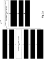
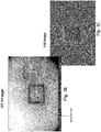
- Figures 3A through 3C are example images of determining offsets between a milled alignment fiducial marker and a probe area in accordance with a disclosed embodiment.
- a first step in determining the offsets may include forming an alignment fiducial marker outside of where the desired probe area may be.
- the desired probe area may be known but its location not precisely known.
- a CAD file showing the location with respect to the corner fiducial markers may be known.
- the system may move the stage to an area outside of the desired probe area based on the CAD file and the obtained IR image of the corner fiducial markers.
- the alignment fiducial marker may be milled into the backside surface of the IC using offsets ⁇ x and ⁇ y from the desired probe area, or what is assumed to be above the desired probe area.
- Figure 3A shows the suspected location of the probe area, the offsets ⁇ x and ⁇ y, and the alignment fiducial marker milled into the backside of an IC.
- the infrared imaging system is used to locate the milled alignment fiducial marker and the desired probe location. See Figure 3B for an IR image.
- the system measures where the desired probe location is with relation to the alignment fiducial marker and adjusted offsets ⁇ X and ⁇ Y are determined.
- the adjusted offsets should be more exact than the initial guess offsets.
- the remaining substrate is milled to fully uncover the desired probe area.
- a box centered on the adjusted offsets is milled.
- multiple boxes of decreasing area may be milled to fully uncover the desired probe area, as seen in Figures 3B and 3C .
- the area being milled is shown as a "box," e.g., a square or rectangle, the shape of the area being milled is not so limited. In general, any geometrical shape may be used to define the target milling area. In other embodiments, the target milling area may be define by a target volume, which may be further defined by a pixel-by-pixel milling depth.
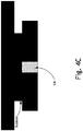
- FIGS. 4A, 4B and 4C are example heatsinking configurations in accordance with embodiments of the present disclosure. Because active ICs under electrical test create heat, the removal of the heat is generally desired to reduce thermal expansion and drift, and to improve device testing environment, for example. However, the removal of this heat poses challenges in the vacuum systems required of electron and ion beam systems. Further, thermal drift caused by this heat will need to be accounted and compensated for during the time it takes to measure electrical activity on the IC. As a result, the IC devices for electrical probing may be prepared with the requirements of heat removal and thermal drift accounted for.
- One technique for removing heat involves thinning the substrate uniformly to a known thickness, such as ten microns as described earlier.
- the entire sample is uniformly thinned, this enables mating a heat sinking material to the thinned IC to remove heat from the active IC, as shown in Figure 4A .
- Such heat could be transferred laterally off the IC to a surrounding region.
- the load board could be thermally coupled to, and dissipate heat from, the DUT via the DUT's heat sinking material 405.
- the load board could contain its own heatsink embedded within it (not shown), such as a thick copper plane, or gas, liquid, or phase-change means of removing heat from the load board, with the DUT heatsink 405 in thermal connection with the load board heat sink, such that the final objective of keeping the DUT cooled is achieved.
- said DUT heat sink could contain a via, such as a hole, several holes, a slot, multiple slots, and the like, through which ion milling and e-beam probing can occur.
- the load board may have an aperture that can be aligned to the via in the heatsink 405. While the figure shows the via and the aperture commensurate in size, e.g., diameter, the size of each opening may be different.
- An alternate method of sample preparation could involve mechanically opening up a small region, e.g., a via, of an IC, as shown in Figure 4B .
- a full-thickness IC is typically built on silicon substrates that are 760 microns thick. Such thick substrates effectively disperse heat and it may be advantageous to leave the IC at full thickness for reasons of heat dissipation and removal, however the device still needs to be electrically probed. This may represent a case where a small region could be milled into the full-thickness device, thereby enabling electrical probing of a small region while the remainder of the IC is cooled as originally designed. Alternatively the IC having just a small region milled may also be thermally coupled to a heat sink for improved thermal dissipation.
- the DUT may be coupled to a thermally conductive gasket 408 to provide a vacuum interface so that the DUT is thermally coupled to the vacuum chamber. See Figure 4C .
- the vacuum chamber provides the heat sinking through the thermally conductive gasket 408, which may reduce the need for a heat sink included in the load board and another coupled to the DUT as shown in Figures 4A, 4B .
- thermal drift between the DUT and the charged particle columns may present a system stability challenge. For instance, it may take tens of minutes to make a complex measurement, and during that time a single 10-nm transistor may need to be imaged continually, thus a means of compensating for the thermal drift will be required.
- Several such methods to compensate for thermal drift are known by those skilled in the art of microscopy, as are mechanical and electrical means of compensating for vibration, and those technique will not be described herein.
Landscapes
- Physics & Mathematics (AREA)
- General Physics & Mathematics (AREA)
- Engineering & Computer Science (AREA)
- Analytical Chemistry (AREA)
- Chemical & Material Sciences (AREA)
- Plasma & Fusion (AREA)
- Microelectronics & Electronic Packaging (AREA)
- General Engineering & Computer Science (AREA)
- Computer Hardware Design (AREA)
- Health & Medical Sciences (AREA)
- Pathology (AREA)
- Immunology (AREA)
- General Health & Medical Sciences (AREA)
- Biochemistry (AREA)
- Life Sciences & Earth Sciences (AREA)
- Testing Or Measuring Of Semiconductors Or The Like (AREA)
- Analysing Materials By The Use Of Radiation (AREA)
Abstract
Description
- This invention relates to the diagnosis and characterization of electrically active integrated circuits using charged particle beams, and to the probing of electrical activity from the backside of modern integrated circuitry while they are being electrically stimulated by a testing means. More specifically, the invention describes a system and method for preparing modern finFET integrated circuits to enable electron-beam waveform probing.
- Integrated Circuits (ICs) undergo electrical device characterization throughout their design and manufacturing life cycle to verify that the ICs are meeting their performance expectations. An IC not meeting design performance expectations may undergo a debugging and failure analysis process to determine the root cause of its non-conformance. The field of electrical failure analysis involves the diagnosis and characterization of electrically active IC devices for the purpose of identifying the root cause of such non-conformances.
-
-
Figure 1A is an example chargedparticle beam system 100 in accordance with an embodiment of the present disclosure. -
Figure 1B is an example IC 150 in accordance with an embodiment of the present disclosure. -
Figure 2 is a flow chart of anexample method 200 in accordance with an embodiment of the present disclosure. -
Figures 3A through 3C are example images of determining offsets between a milled alignment fiducial marker and a probe area in accordance with a disclosed embodiment. -
Figures 4A and 4B are example heatsinking configurations in accordance with a disclosed embodiment. - Like reference numerals refer to corresponding parts throughout the several views of the drawings.
- As used in this application and in the claims, the singular forms "a," "an," and "the" include the plural forms unless the context clearly dictates otherwise. Additionally, the term "includes" means "comprises." Further, the term "coupled" does not exclude the presence of intermediate elements between the coupled items.
- The systems, apparatus, and methods described herein should not be construed as limiting in any way. Instead, the present disclosure is directed toward all novel and non-obvious features and aspects of the various disclosed embodiments, alone and in various combinations and sub-combinations with one another. The disclosed systems, methods, and apparatus are not limited to any specific aspect or feature or combinations thereof, nor do the disclosed systems, methods, and apparatus require that any one or more specific advantages be present or problems be solved. Any theories of operation are to facilitate explanation, but the disclosed systems, methods, and apparatus are not limited to such theories of operation.
- Although the operations of some of the disclosed methods are described in a particular, sequential order for convenient presentation, it should be understood that this manner of description encompasses rearrangement, unless a particular ordering is required by specific language set forth below. For example, operations described sequentially may in some cases be rearranged or performed concurrently. Moreover, for the sake of simplicity, the attached figures may not show the various ways in which the disclosed systems, methods, and apparatus can be used in conjunction with other systems, methods, and apparatus. Additionally, the description sometimes uses terms like "produce" and "provide" to describe the disclosed methods. These terms are high-level abstractions of the actual operations that are performed. The actual operations that correspond to these terms will vary depending on the particular implementation and are readily discernible by one of ordinary skill in the art.
- In some examples, values, procedures, or apparatus' are referred to as "lowest", "best", "minimum," or the like. It will be appreciated that such descriptions are intended to indicate that a selection among many used functional alternatives can be made, and such selections need not be better, smaller, or otherwise preferable to other selections.
- The current state of the art in electrical device characterization uses optical lasers focused on individual transistors within an IC to measure electrical activity within an active IC. See for example Kindereit, Ulrike, "Fundamentals and Future Applications of Laser Voltage Probing", IEEE Reliability Physics Symposium, pp. 1-11, Jun. 2014. A limitation of optical probing techniques, however, is that they are unable to resolve features substantially smaller than the wavelength of the light used in the optical probe, and despite a recent push to shorten the wavelength and use visible optical probing techniques (see, for example,
U. S. Patent 9,651,610 B2 - Diagnostic tools able to perform electrical device characterization of ICs using charged particle beams have existed for several decades. For example,
U. S. Patent 4,706,019 filed in 1985 discloses an electron beam test probe system for analyzing ICs from their front side. During the 1990s, however, advanced ICs became packaged in a "flip-chip" state where access to the front active side of an active IC was no longer possible, and this advance in packaging led to a need to probe ICs from their back substrate side.U. S. Patent 5,972,725 (hereafter '725) discloses a method of precisely measuring electrical parameters from the back substrate side of an IC by using a scanning electron microscope probe directed at active regions of the IC exposed by the removal of the semiconductor substrate.U. S. Patent 6.872,581 (hereafter '581) discloses a method of probing active ICs from their back substrate side using charged particle beams - electron or ion beams - directed at a thinned substrate layer where electrical activity beneath the thinned substrate layer induces an electrical potential on the outer surface that is probed by the charged particle beam. Thus '725 teaches a method of using a scanning electron microscope to measure electrical activity from the backside of an IC by thinning the substrate all the way to the active regions of the IC, while '581 allows that either an electron or an ion microscope can probe electrical activity from a surface near, but not at, the active regions of the IC. - In the fifteen to twenty years since the '581 and '725 patents were issued, advanced semiconductor manufacturers have transitioned from bulk active devices that could extend over one micron in depth into their silicon substrate to a tri-gate (also known as a finFET) transistor architecture. A typical tri-gate transistor in an advanced IC will consist of a fin of silicon that is of order ten nanometers wide, fifty nanometers tall, and having a gate that is of order ten or fewer nanometers long. As a result, electrical activity within active silicon resides within the topmost fifty nanometers of the IC substrate. To prepare such a sample for charged particle probing, the substrate material needs to be removed to expose the bottom side of the fins of silicon that comprise the active transistors of the IC. The '725 patent envisioned removing the bulk substrate to a region approximately one micron from the front side of the IC, while the '581 method envisioned removing the bulk substrate to within one to three microns. With modern tri-gate transistors, however, the substrate must be removed to within approximately fifty nanometers of the front side of the IC, with a tolerance of only ten or twenty nanometers, and such sample preparation presents a challenge that was not anticipated by the '581 and '725 patents. If too little substrate material is removed, the individual transistor fins are not exposed and cannot be electrically exposed, yet if too much substrate material is removed, the transistor fins themselves will be removed, thereby preventing their electrical characterization.
- We disclose a system and method for preparing modern tri-gate semiconductor ICs so that their electrical activity can be probed using charged particle beams. Charged particle beam microscopy can easily resolve feature sizes of one nanometer and below, which is a one hundred-fold improvement over the best resolution achieved with optical microscopy and laser voltage probing. The technique described enables the removal of substrate silicon from the IC all the way down to, but not through, the active transistor fins of the IC.
- The following describes techniques for preparing modern tri-gate semiconductor ICs so that their electrical activity can be probed using charged particle beams. Embodiments are disclosed to achieve this goal, but the method described herein should not be restrictive as those skilled in the art will understand that various modifications to the process may be made without departing from the spirit of this invention. For instance, the techniques described herein could also be used to prepare future semiconductor ICs that use next-generation gate-all-around (GAA) transistors, nanowire transistors, three dimensional IC structures, transistors that are not built using silicon, and in general, any substrate thinning process that requires very precise endpoint detection to effect device characterization using charged particle techniques.
- A conventional IC may be patterned and built on the front side of a silicon substrate, with the substrate being approximately 760 microns thick. For modern ICs, as discussed above, the active circuitry comprises fin-shaped tri-gate transistors that reside within approximately fifty nanometers of the silicon surface. Processes are disclosed for the removal of nearly the entirety of this substrate material so that in the end only the active transistors remain and the IC remains electrically functional.
- Conventionally, ICs are tested by attaching them to a printed circuit board known as a load board. The load board, in turn, typically connects to an automated electrical tester that powers the IC and supplies electrical test signals, and, in some embodiments, the load board will form a sliding vacuum seal required to both position the device under test (DUT) relative to the charged-particle beams, and to maintain needed vacuum integrity within the microscope. If the IC needs to be soldered to the load board for electrical testing, it should be soldered to the board before any other sample preparation steps are taken because the thermal stress of the soldering process can damage thinned IC devices, e.g., ICs having bulk material removed to expose all or some of the active structure.
-
Figure 1A is an example chargedparticle beam system 100 in accordance with an embodiment of the present disclosure. Thesystem 100 may be a dual-beam system, as known in the art. For example, thesystem 100 may include both an electron beam column and an ion beam column. The column labeled SEM may include an electron emitter, such as a Schottky emitter, various lenses for focusing the electron beam, and detectors. The detectors may be used to detect backscattered and secondary electrons, for example, but other photon-centric detectors may also be included, such as ultraviolet, visible, and infrared light detectors and/or x-ray detectors. The ion beam column, labeled as such inFigure 1A , includes an ion source, such as a plasma or liquid metal ion source, along with focusing optics for shaping the ion beam. The detectors discussed above in relation with the SEM column may also be used in conjunction with the ion beam column. For example, secondary electrons and/or secondary ions may be detected when the sample is subject to an ion beam. - The
system 100 further includes an infrared imaging system for locating regions of interest in the active area of thesample 102. The regions of interest are areas where one or more transistors, e.g., finFETs, are to be analyzed. Locating the one or more transistors helps thesystem 100 navigate to the area that requires additional processing to expose the regions of interest. The infrared imaging system at least includes a retractable mirror and an infrared camera, labeled IR inFigure 1A . Additionally (and not shown), the infrared imaging system includes a suitable IR source for projecting IR light through a sample and towards the retractable mirror. - The
system 100 also includes an electrical tester that can be coupled to an IC under test (e.g., sample 102), which may also be referred to as a device under test (DUT). The electrical tester may provide clock and/or data signals to one or more functional blocks of the IC device to drive the transistors of the functional block. One or more of the transistors of a designated area, e.g., region of interest, may desirably be examined for failure mechanisms, and which may be excavated by ion milling, for example, for specific testing. The excavation of the transistors may be performed as disclosed herein. - The
system 100 also includes other ancillary equipment for producing a low pressure environment required for operating the ion beam and SEM columns. For example, a vacuum seal may seal thesample 102 and electrical tester to the SEM column, ion beam column, and infrared imaging system. To generate the low pressure/high vacuum environment, thesystem 100 includes a turbo pump, and one or more ion pumps, all coupled to the vacuum chamber. A stage may be included in the vacuum chamber to manipulate the location of the ion beam and SEM columns, thesample 102, or both. The stage may be moved in at least three degrees of freedom, but additional degrees may also be included allowing for both translational and rotational movement. - Additionally, the
system 100 includes a controller coupled to the ion beam column, the SEM column, the detectors, the infrared imaging system, the electrical tester, and the vacuum pumps. The controller is coupled to control operation of the various components for implementing the techniques disclosed herein. For example, themethod 200, discussed in detail below, may use the SEM, detectors, and ion beam columns along with the infrared imaging system to prepare thesample 102 for electrical testing. Specifically, themethod 200 may include locating a desired probe location, milling substrate material to uncover the probe location, and end point detection to determine when a transistor to test has been uncovered. The end point detection may be sensitive enough to remove oxide material without detrimentally affecting the transistor regions so that electrical testing may occur while physical probing of the transistor occurs, such as with optical or electron beam techniques. - The
sample 102, which may be thermally managed, is coupled to a load board. The load board is coupled to the electrical tester, and thesample 102. The load board relays electrical test signals from the electrical tester to thesample 102.Figure 1A shows an example location for the load board. In other embodiments, the load board may be on the bottom side of thesample 102. In some embodiments, the load board may be used for coupling the vacuum chamber to the electrical tester and may include at least two dimensional alignment mechanics. In some embodiments, the load board may include heat sinking and heat exchange aspects to remove heat from thesample 102. For example, the load board may include a fluid heat exchanger or a thick copper plane, but other techniques may also be implemented. -
Figure 1B is anexample IC 102 in accordance with an embodiment of the present disclosure. TheIC 102, which may also be simply referred to assample 102, includes asubstrate 120 and anactive area 130. Thesubstrate 120 may be formed from any known semiconductor material, such as silicon, GaAs, InP, Ge, GaN, etc. While silicon is used to illustrate the disclosure, the disclosure is not limited as such. Theactive area 130 may include one or more levels of active circuitry, such as transistors coupled by metal traces. In some examples, the transistors are finFETs, as discussed herein. However, while the disclosed processing techniques may be advantageous for finFET processing, the techniques are not limited by the transistor technology. As used herein, a backside of thesample 102 is the substrate side whereas a front side of thesample 102 is theactive area 130 side. -
Figure 2A is a flow chart of anexample method 200 in accordance with an embodiment of the present disclosure. Themethod 200 may be implemented on thesystem 100, for example, to at least partially prepare and locate a desired transistor, circuit(s), electrical trace, or combinations thereof, of a sample or IC, such as thesample 102, to undergo electrical testing. While some of the preparation steps may be performed in theexample system 100, other steps may be performed outside of and prior to loading an IC into thesystem 100. For example, bulk removal of substrate material may be performed prior to loading the sample into thesystem 100. While not all examples of sample preparations, e.g., material removal and end point detection, are explicitly covered herein, they are within the bounds of the present disclosure and fully contemplated. - The
method 200 may begin at step 201, which includes the bulk removal of substrate material from a back side of an IC or sample. The IC or sample may be formed in or from silicon, GaAs, InP, Ge, or any semiconductor material. While silicon may be used as an illustrative example in the disclosure, the disclosure should not be considered so limited. The bulk removal may be implemented using one or more mechanical techniques, such as lapping, milling, polishing, or may be implemented using other techniques commonly used to thin semiconductor substrates, such as laser ablation, chemical etching, etc. In some embodiments, a combination of techniques may be used to remove the bulk substrate material. Also known to those skilled in the art of preparing samples are tools for accurately measuring residual substrate thickness after the milling process. In some embodiments, the substrate need not be thinned over the entire region of the IC, and the thinning may be confined to an area above a region of interest, e.g., a desired probing region in an active area disposed on an opposite side of the IC. For example, a small pocket can be formed within the IC substrate using one or more mechanical milling techniques. In some embodiments, the bulk removal of the substrate may include removal of substrate across an entire backside of an IC or sample. In other embodiments, the bulk removal may be performed in a small area on the backside above a desired probe area, e.g., a region of interest. - The step 201 may be followed by the step 203, which includes polishing the backside of the IC or sample. The polishing may be performed using any known method for wafer material polishing, such as using a slurry and polishing pad. In some embodiments, it may be desirable for the polishing step to result in an optically smooth surface. As an example, thinning an IC or sample to approximately 20 microns residual thickness of substrate material using a mechanical technique, then removing another 10 microns in a polishing process that progressively uses finer polishing compounds results in an IC with approximately ten microns of residual silicon substrate having an optically smooth sub-micron surface roughness. The optically smooth sub-micron surface roughness may be desirable to reduce or eliminate uneven exposure of the active transistor fins post a subsequent thinning step, such as a plasma-based thinning process. If the residual silicon is substantially thicker than ten microns after polishing (e.g., 15 microns or more residual thickness), then the subsequent thinning process may require excessive time to complete. On the other hand, if the residual silicon after polishing is substantially thinner than ten microns (e.g., 5 microns or less), the subsequent thinning process may not eliminate the surface roughness left after the mechanical polishing process and will lead to uneven exposure of the active transistor fins.
- The step 203 may optionally be followed by
step 205, which includes electrically testing the IC or sample to confirm device functionality. Once proper functionality is confirmed, the IC device can be inserted into a charged particle beam system (step 207). In some embodiments, the charged particle system, such as thesystem 100, may include a scanning electron microscope for imaging and electrically probing nanometer features on the IC, a focused ion beam tool capable of imaging and removing the residual substrate material to the level of the fin transistors, and an infrared imaging system capable of looking through silicon substrate material to see features that have been patterned onto the IC during its manufacture. In other embodiments, the charged particle system may omit the infrared imaging system. - The step 207 may be followed by the step 209, which includes locating corner fiducials that have been patterned onto the IC surface during its manufacture. In some embodiments, the corner fiducials may be observed by looking through the silicon substrate using the infrared camera, which may allow the corner fiducials, which are on the front side, be located. The infrared camera must have an infrared illumination source to illuminate the IC for inspection. The infrared camera is used to determine and calibrate an offset between the known corner fiducials that are visible beneath the substrate, e.g., on the front side, and other fiducials, such as chip corners, that can be observed using electron and ion beam imaging, neither of which can image through the remaining substrate material and image the corner fiducials on the front side of the IC.
- Step 209 may be followed by the step 211, which includes calibrate offsets to determine between fiducial features observable by electron and ion beam imaging and fiducial features observable through the substrate using infrared imaging. Once calibrated offsets have been determined, see
Figures 3A through 3C for detail, between fiducial features observable by electron and ion beam imaging, and fiducial features observed through the substrate using the infrared imager, a mechanical stage system can move to any location on the IC. For example, a debug technique will specify a region of the IC to be probed, and the coordinates of that region will be known. The region of the IC to be probed could be an individual transistor, a small circuit comprised of several transistors, a region containing many circuits, or even a metal trace of the IC. With the coordinates of the region to be probed, and having the calibrated offsets as described, mechanical stages can move the IC to position the known probe location in an optimal location to be acted upon by the focused ion beam tool. - The step 211 may be followed by the
step 213, which includes navigating to a region outside of the probe location, e.g., the region of interest, and milling an alignment fiducial marker on the backside surface of the IC. The alignment fiducial may reduce or eliminate possible navigation errors by helping more accurately determine where the probe location and final milling should be performed. The milling of the alignment fiducial, in some embodiments, may be performed using a focused ion beam tool, which may be a plasma-based ion mill. For example, a 5 micron square region 0.5 microns deep is easily observed in all three (e.g., electron, ion, and infrared) imaging modalities. Once such an alignment fiducial marker has been created, an infrared image of this region will be captured (seeFigure 3B , for example), and such an image will clearly show the region where electrical probing is desired, adjacent to the alignment fiducial marker, and a precise offset between these two can be calculated, e.g. ΔX and ΔY. This step may eliminate the navigation uncertainties and errors associated with the previous steps of the process, and provide certainty that the region of the substrate opened up in the following steps may be precisely collocated with the desired electrical probe location. In some embodiments,step 213 may be optional and other methods may be used to more precisely locate the probe location. For example, the backside of the IC may be milled at the corners to locate the corner fiducials and make them observable using electron or ion imaging. Then, the combination of CAD files and the located corner fiducials may be used to locate the probe location. While this alternative method may work, the two extra milling steps to uncover the corner fiducials results in longer processing time, and the end result may be less precise than forming the alignment fiducial. - Step 213 may be followed by the step 215, which includes locating the previously milled alignment fiducial marker and applying the final offset from that milled alignment fiducial marker to identify the region of the substrate over the desired probe location. For example, with the final offset between the alignment fiducial marker and the desired probe location measured, the mechanical stages may again position the IC beneath the focused ion beam where the location may be imaged. Imaging with the ion beam locates the previously milled alignment fiducial marker, and the final offset is applied from that marker to identify the region of the substrate over the desired probe location.
- Step 215 may be followed by the step 217, which includes removal of the residual substrate material over the desired probe location. For example, the focused ion beam can be programmed to remove a desired amount of substrate material over the desired probe location. Because the amount of substrate material to be removed can be accurately measured during the sample preparation phase, and because focused ion beams have a calibrated substrate removal rate, a timed technique may be employed to remove the bulk of the remaining substrate thickness. For instance, if the substrate is known to be ten microns thick, it is common to remove all but one or two microns of substrate material using plasma-based focused ion beam milling over the desired probe region.
- The step 217 may be followed by step 219, which includes detecting the end point of substrate removal to uncover the desired probing area. At the beginning of step 219, very little (e.g., one or two microns) substrate material may remain covering the fin transistors of the IC, e.g., the probe area, and subsequent removal of the material must be monitored to detect when the fin transistors have been reached. As previously mentioned this is a delicate end point detection process with a required tolerance of approximately ten nanometers.
- Various end point techniques may be employed in step 219, as discussed herein and shown in
Figures 2B through 2C , and multiple of those techniques may be combined in one or more embodiments. The various end pointing techniques use a signature of the probe location to determine when to terminate the milling process, wherein the signature indicates that the underlying active layer has been reached, e.g., that a thin layer of the substrate has been milled through to uncover the active layer. One technique involves the monitoring for and detection during the ion milling process of a change in image contrast, seeFigure 2B for an example, to indicate the underlying active layer has been reached during the milling process. Tri-gate transistors consist of narrow fins of silicon surrounded by a silicon dioxide region known as the shallow trench isolation (STI) region. As the ion beam from the focused ion beam mills through substrate material, secondary electrons are emitted by the substrate material and it is those secondary electrons, when captured, create the ion beam image of the substrate surface, seeimage 202 for an example. It is known that the secondary emission rate from silicon differs from that of the STI such that a change in image brightness occurs when this STI region is reached. Further, the STI region between individual fin transistors is more shallow than the STI region between blocks of fin transistors, so the pattern of the STI layer can be used to precisely locate the depth at which the fins become exposed. For example, theSTI region 208 between a block of fin transistors may be uncovered and observable before theSTI region 210 between individual fin transistors within a block, and an image showinginter-block STI 208 may be used to slow the milling to determine when theintrablock STI region 210 appears. This is one method of ending the focused ion beam milling process. - Another method for implementing the step 219 may use optical or x-ray emission of sputtered atoms as indicating an end point to the milling has been reached based on monitoring for and detecting such optical or x-ray emissions. As an example, as the plasma focused ion beam mills away at the substrate, substrate (silicon) atoms will be sputtered off the surface, some of which become electrically excited in the process and can relax to their ground state, emitting light in the process. This process may be referred to as ion-induced light emission. Light emitted from silicon has a different spectrum than light emitted from a sputtered oxygen atom, hence the presence of characteristic spectrum of oxygen atoms can indicate that the milling process has reached one of the STI layers. Similarly, bombardment of the surface with high energy electrons or ions may produce characteristic x-ray signatures identifying the material as either silicon or oxygen, and the presence of oxygen x-ray emissions can similarly identify that the STI layer has been reached.
- Another method for implementing step 219 uses an ion mass spectrometer, for example a residual gas analyzer, to monitor for and detect the presence of oxygen ions in the vacuum chamber when the plasma reaches the STI layer. Such detection indicates that the milling should be stopped due to reaching the underlying STI layer.
- Another method for implementing step 219 involves going back and forth between ion beam milling and electron-beam imaging to monitor for indications that the milling has reached the active layer. Specifically, imaging using backscattered electrons from a higher energy (typically 5 keV or higher), see
Figure 2C for an example, electron source enables the user to see through 50 to 100 nm or more of substrate material, thus when patterned features on the IC surface become visible in the backscattered electron image, it is known that fin transistors are very close to emerging from the substrate, and this information can be used to control the final ion beam milling step. For example, inimage 206, which was obtained with an electron energy of 10 keV,underlying patterns 216 have become visible through a thin (50 to 100 nm) layer ofsilicon 214. The initial visibility of the underlying patterns at high electron energy, as noted, provides guidance regarding the amount, e.g., thickness, of the overlying layer, which may then guide subsequent milling steps. - Yet another method for implementing step 219 involves looking for voltage contrast in the scanning electron microscope image as the device is thinned using the ion beam. This has two possible forms. A first form, and one known in the art, includes the use of voltage contrast imaging, see
Figure 2D for an example. For example, since the IC is powered, it can be placed in a state with known potentials on known circuitry, and the technique of voltage contrast imaging, which is known to all skilled in the art of electron microscopy, can be used to detect close proximity to active circuitry. Such techniques were disclosed in the '581 and '725 patents. Inimage 204, voltage contrast mapping showscircuits 212 beginning to be visible through an overlying layer do to thinning of that overlying layer. It should also be noted thatimage 204 is the voltage contrast image ofimage 202. - A second and new form enables alternating potentials to be easily measured from active fin transistors. This technique is the electron-beam analog of the optical technique disclosed in
U. S. Patent 9,239,357 Image 204 provides an example of the outcome of this technique as well, but the steps taken to obtain such an image will be as discussed in this paragraph as opposed to the preceding paragraph. -
Figures 3A through 3C are example images of determining offsets between a milled alignment fiducial marker and a probe area in accordance with a disclosed embodiment. A first step in determining the offsets may include forming an alignment fiducial marker outside of where the desired probe area may be. As discussed above, the desired probe area may be known but its location not precisely known. However, a CAD file showing the location with respect to the corner fiducial markers may be known. As such, the system may move the stage to an area outside of the desired probe area based on the CAD file and the obtained IR image of the corner fiducial markers. At this area, the alignment fiducial marker may be milled into the backside surface of the IC using offsets Δx and Δy from the desired probe area, or what is assumed to be above the desired probe area.Figure 3A shows the suspected location of the probe area, the offsets Δx and Δy, and the alignment fiducial marker milled into the backside of an IC. - Subsequently, the infrared imaging system is used to locate the milled alignment fiducial marker and the desired probe location. See
Figure 3B for an IR image. Using the infrared image, the system measures where the desired probe location is with relation to the alignment fiducial marker and adjusted offsets ΔX and ΔY are determined. The adjusted offsets should be more exact than the initial guess offsets. - Based on the adjusted offsets ΔX and ΔY, the remaining substrate is milled to fully uncover the desired probe area. For example, a box centered on the adjusted offsets is milled. In some embodiments, multiple boxes of decreasing area may be milled to fully uncover the desired probe area, as seen in
Figures 3B and 3C . While the area being milled is shown as a "box," e.g., a square or rectangle, the shape of the area being milled is not so limited. In general, any geometrical shape may be used to define the target milling area. In other embodiments, the target milling area may be define by a target volume, which may be further defined by a pixel-by-pixel milling depth. -
Figures 4A, 4B and4C are example heatsinking configurations in accordance with embodiments of the present disclosure. Because active ICs under electrical test create heat, the removal of the heat is generally desired to reduce thermal expansion and drift, and to improve device testing environment, for example. However, the removal of this heat poses challenges in the vacuum systems required of electron and ion beam systems. Further, thermal drift caused by this heat will need to be accounted and compensated for during the time it takes to measure electrical activity on the IC. As a result, the IC devices for electrical probing may be prepared with the requirements of heat removal and thermal drift accounted for. One technique for removing heat involves thinning the substrate uniformly to a known thickness, such as ten microns as described earlier. If the entire sample is uniformly thinned, this enables mating a heat sinking material to the thinned IC to remove heat from the active IC, as shown inFigure 4A . Such heat could be transferred laterally off the IC to a surrounding region. For example, if the DUT is mounted to a load board, the load board could be thermally coupled to, and dissipate heat from, the DUT via the DUT's heat sinking material 405. To accomplish this, the load board could contain its own heatsink embedded within it (not shown), such as a thick copper plane, or gas, liquid, or phase-change means of removing heat from the load board, with the DUT heatsink 405 in thermal connection with the load board heat sink, such that the final objective of keeping the DUT cooled is achieved. Further, said DUT heat sink could contain a via, such as a hole, several holes, a slot, multiple slots, and the like, through which ion milling and e-beam probing can occur. Moreover, to provide access to the DUT for testing and probing, the load board may have an aperture that can be aligned to the via in the heatsink 405. While the figure shows the via and the aperture commensurate in size, e.g., diameter, the size of each opening may be different. - An alternate method of sample preparation could involve mechanically opening up a small region, e.g., a via, of an IC, as shown in
Figure 4B . For instance, a full-thickness IC is typically built on silicon substrates that are 760 microns thick. Such thick substrates effectively disperse heat and it may be advantageous to leave the IC at full thickness for reasons of heat dissipation and removal, however the device still needs to be electrically probed. This may represent a case where a small region could be milled into the full-thickness device, thereby enabling electrical probing of a small region while the remainder of the IC is cooled as originally designed. Alternatively the IC having just a small region milled may also be thermally coupled to a heat sink for improved thermal dissipation. - In other embodiments, the DUT may be coupled to a thermally conductive gasket 408 to provide a vacuum interface so that the DUT is thermally coupled to the vacuum chamber. See
Figure 4C . In such an embodiment, the vacuum chamber provides the heat sinking through the thermally conductive gasket 408, which may reduce the need for a heat sink included in the load board and another coupled to the DUT as shown inFigures 4A, 4B . - Owing to the heat generated by the DUT, as well as the nanometer-scale dimensions of the fin transistors themselves, it is anticipated that thermal drift between the DUT and the charged particle columns may present a system stability challenge. For instance, it may take tens of minutes to make a complex measurement, and during that time a single 10-nm transistor may need to be imaged continually, thus a means of compensating for the thermal drift will be required. Several such methods to compensate for thermal drift are known by those skilled in the art of microscopy, as are mechanical and electrical means of compensating for vibration, and those technique will not be described herein.
- Having described and illustrated the principles of the disclosed technology with reference to the illustrated embodiments, it will be recognized that the illustrated embodiments can be modified in arrangement and detail without departing from such principles. For instance, elements of the illustrated embodiments shown in software may be implemented in hardware and vice-versa. Also, the technologies from any example can be combined with the technologies described in any one or more of the other examples. It will be appreciated that procedures and functions such as those described with reference to the illustrated examples can be implemented in a single hardware or software module, or separate modules can be provided. The particular arrangements above are provided for convenient illustration, and other arrangements can be used.
- In view of the many possible embodiments to which the principles of the disclosed technology may be applied, it should be recognized that the illustrated embodiments are only representative examples and should not be taken as limiting the scope of the disclosure. Alternatives specifically addressed in these sections are merely exemplary and do not constitute all possible alternatives to the embodiments described herein. For instance, various components of systems described herein may be combined in function and use. We therefore claim all that comes within the scope of the appended claims.
Claims (16)
- A method comprising:removing bulk material from a backside of a sample, a front side of the sample including an active layer, wherein removal of the bulk material leaves a thin layer of the bulk material covering the active layer on the backside;milling, by an ion beam, the thin layer to expose a probe area of the active layer;monitoring the milling of the thin layer based on a signature of the probe location indicating that the active layer has been reached; andterminating, in response to the monitoring, the milling.
- The method of claim 1, wherein monitoring the milling of the thin layer based on a signature of the probe location indicating that the active layer has been reached comprises:
detecting an image contrast while milling the thin layer, the image contrast indicating the active layer has been reached. - The method of claim 2, wherein detecting an image contrast while milling the remaining material from the backside of the sample comprises:
detecting a change in image brightness between components in the probe area formed of silicon oxide and components in the probe area formed of silicon. - The method of claim 1, wherein monitoring the milling of the thin layer based on a signature of the probe location indicating that the active layer has been reached comprises one or more of the following:- detecting ion induced light emission from atoms sputtered off the backside, wherein oxygen provides a different light emission than silicon, and wherein oxygen indicates the active layer has been reached;- detecting characteristic x-ray signatures to identify material on the surface of the backside, wherein detection of oxygen indicates the active layer has been reached;- detecting presence of oxygen atoms in the vacuum chamber using ion mass spectroscopy, wherein the presence of oxygen indicates the active layer has been reached.
- The method of claim 1, wherein monitoring the milling of the thin layer based on a signature of the probe location indicating that the active layer has been reached comprises:
alternating between the milling of thin layer and electron-beam imaging of the backside to determine when an underlying pattern of the active layer is within 10 to 100 nm from the surface to calibrate and slow the milling of the thin layer, wherein the electron beam imaging is performed at energies of at least 5 keV. - The method of claim 1, wherein monitoring the milling of the thin layer based on a signature of the probe location indicating that the active layer has been reached comprises:establishing voltage potentials on the active layer for voltage contrast imaging; anddetecting voltage contrast in scanning electron microscope images of the backside of the sample as the milling of the thin layer is performed.
- The method of claim 1, further comprising:locating corner fiducials on a front side of the sample using an infrared imaging system;locating the probe area based on coordinates provided by a debug control;locating a region outside of the probe area;milling an alignment fiducial on the backside of the sample in the region outside of the probe area;imaging the probe area and the alignment fiducial using the infrared system;determining an offset between the alignment fiducial and the probe area based on the imaging; andlocating the probe location based on the offset.
- The method of claim 1, further comprising:polishing the backside of the sample after removal of the bulk material; andLoading the sample into a chamber.
- A system comprising:an electron beam column to provide an electron beam;an ion beam column to provide an ion beam;one or more detectors; anda controller coupled to the electron and ion beam columns, the controller configured to:mill, by the ion beam, a thin layer to expose a probe area of the active layer;monitor the milling of the thin layer based on a signature of the probe location indicating that the active layer has been reached; andterminate, in response to the monitoring, the milling.
- The system of claim 9, wherein to monitor the milling of the thin layer based on the signature of the probe location indicting that the active layer has been reached further includes the controller configured to:
detect an image contrast while milling the thin layer, the image contrast indicating the active layer has been reached. - The system of claim 9, wherein to detect an image contrast while milling the remaining material from the backside of the sample further includes the controller configured to:
detect a change in image brightness between components in the probe area formed of silicon oxide and components in the probe area formed of silicon. - The system of claim 9, wherein to monitor the milling of the thin layer based on the signature of the probe location indicting that the active layer has been reached further includes the controller configured to:
detect ion induced light emission from atoms sputtered off the backside, wherein oxygen provides a different light emission than silicon, and wherein oxygen indicates the active layer has been reached. - The system of claim 9, wherein to monitor the milling of the thin layer based on the signature of the probe location indicting that the active layer has been reached further includes the controller configured to one or more of the following:- detect characteristic x-ray signatures to identify material on the surface of the backside, wherein detection of oxygen indicates the active layer has been reached; or- detect presence of oxygen atoms in the vacuum chamber using ion mass spectroscopy, wherein the presence of oxygen indicates the active layer has been reached.
- The system of claim 9, wherein to monitor the milling of the thin layer based on the signature of the probe location indicting that the active layer has been reached further includes the controller configured to:
alternate between the milling of thin layer and electron-beam imaging of the backside to determine when an underlying pattern of the active layer is within 10 to 100 nm from the surface to calibrate and slow the milling of the thin layer, wherein the electron beam imaging is performed at energies of at least 5 keV. - The system of claim 9, wherein to monitor the milling of the thin layer based on the signature of the probe location indicting that the active layer has been reached further includes the controller configured to:establish voltage potentials on the active layer for voltage contrast imaging; anddetect voltage contrast in scanning electron microscope images of the backside of the sample as the milling of the thin layer is performed.
- The system of claim 9, wherein the controller is further configured to:Locate corner fiducials on a front side of the sample using an infrared imaging system;locate the probe area based on coordinates provided by a debug control;locate a region outside of the probe area;mill an alignment fiducial on the backside of the sample in the region outside of the probe area;image the probe area and the alignment fiducial using the infrared system;determine an offset between the alignment fiducial and the probe area based on the imaging; andlocate the probe location based on the offset.
Applications Claiming Priority (1)
| Application Number | Priority Date | Filing Date | Title |
|---|---|---|---|
| US201862621819P | 2018-01-25 | 2018-01-25 |
Publications (2)
| Publication Number | Publication Date |
|---|---|
| EP3528277A2 true EP3528277A2 (en) | 2019-08-21 |
| EP3528277A3 EP3528277A3 (en) | 2019-11-20 |
Family
ID=65200720
Family Applications (1)
| Application Number | Title | Priority Date | Filing Date |
|---|---|---|---|
| EP19153236.5A Pending EP3528277A3 (en) | 2018-01-25 | 2019-01-23 | System and method of preparing integrated circuits for backside probing using charged particle beams |
Country Status (4)
| Country | Link |
|---|---|
| US (2) | US20190287762A1 (en) |
| EP (1) | EP3528277A3 (en) |
| KR (1) | KR102741657B1 (en) |
| CN (1) | CN110085530B (en) |
Families Citing this family (7)
| Publication number | Priority date | Publication date | Assignee | Title |
|---|---|---|---|---|
| TWI755883B (en) * | 2020-10-06 | 2022-02-21 | 力晶積成電子製造股份有限公司 | Sample preparation method and sample preparation system |
| EP3982134B1 (en) * | 2020-10-12 | 2024-09-18 | AT & S Austria Technologie & Systemtechnik Aktiengesellschaft | Automated quality testing of component carrier structure after removing material |
| CN113325017A (en) * | 2021-06-02 | 2021-08-31 | 苏州鑫之博科技有限公司 | Equipment for high-energy beam processing and secondary electron detection method |
| US11694934B2 (en) * | 2021-09-21 | 2023-07-04 | Applied Materials Israel Ltd. | FIB delayering endpoint detection by monitoring sputtered materials using RGA |
| US12622229B2 (en) | 2022-08-03 | 2026-05-05 | Nxp Usa, Inc. | Structure and method for test-point access in a semiconductor |
| DE102023125746B3 (en) | 2023-09-22 | 2025-01-16 | Carl Zeiss Microscopy Gmbh | Camera system and method for imaging and navigating an object in a microscope system |
| US20250290834A1 (en) * | 2024-03-15 | 2025-09-18 | Fei Company | Preparation of planar lamella from a multi-layer structure |
Citations (5)
| Publication number | Priority date | Publication date | Assignee | Title |
|---|---|---|---|---|
| US4706019A (en) | 1985-11-15 | 1987-11-10 | Fairchild Camera And Instrument Corporation | Electron beam test probe system for analyzing integrated circuits |
| US5972725A (en) | 1997-12-11 | 1999-10-26 | Advanced Micro Devices, Inc. | Device analysis for face down chip |
| US6872581B2 (en) | 2001-04-16 | 2005-03-29 | Nptest, Inc. | Measuring back-side voltage of an integrated circuit |
| US9239357B2 (en) | 2005-08-26 | 2016-01-19 | Dcg Systems, Inc. | System and method for modulation mapping |
| US9651610B2 (en) | 2013-06-29 | 2017-05-16 | Intel Corporation | Visible laser probing for circuit debug and defect analysis |
Family Cites Families (18)
| Publication number | Priority date | Publication date | Assignee | Title |
|---|---|---|---|---|
| US5252516A (en) * | 1992-02-20 | 1993-10-12 | International Business Machines Corporation | Method for producing interlevel stud vias |
| US5948217A (en) * | 1996-12-20 | 1999-09-07 | Intel Corporation | Method and apparatus for endpointing while milling an integrated circuit |
| US5905266A (en) * | 1996-12-19 | 1999-05-18 | Schlumberger Technologies, Inc. | Charged particle beam system with optical microscope |
| KR100979071B1 (en) * | 2002-02-22 | 2010-08-31 | 에이저 시스템즈 인크 | Chemical Mechanical Polishing of Double Oriented Polycrystalline Materials |
| US6855622B2 (en) * | 2002-05-30 | 2005-02-15 | Nptest, Llc | Method and apparatus for forming a cavity in a semiconductor substrate using a charged particle beam |
| US6958248B1 (en) * | 2003-02-28 | 2005-10-25 | Credence Systems Corporation | Method and apparatus for the improvement of material/voltage contrast |
| US7135123B1 (en) * | 2004-01-14 | 2006-11-14 | Credence Systems Corporation | Method and system for integrated circuit backside navigation |
| KR20060043141A (en) | 2004-02-23 | 2006-05-15 | 지벡스 코포레이션 | Charged particle beam device probe manipulator |
| US7297965B2 (en) * | 2004-07-14 | 2007-11-20 | Applied Materials, Israel, Ltd. | Method and apparatus for sample formation and microanalysis in a vacuum chamber |
| US7612321B2 (en) * | 2004-10-12 | 2009-11-03 | Dcg Systems, Inc. | Optical coupling apparatus for a dual column charged particle beam tool for imaging and forming silicide in a localized manner |
| US7388218B2 (en) * | 2005-04-04 | 2008-06-17 | Fei Company | Subsurface imaging using an electron beam |
| JP4181561B2 (en) * | 2005-05-12 | 2008-11-19 | 松下電器産業株式会社 | Semiconductor processing method and processing apparatus |
| US7535000B2 (en) * | 2006-05-23 | 2009-05-19 | Dcg Systems, Inc. | Method and system for identifying events in FIB |
| JP5756585B2 (en) * | 2010-04-07 | 2015-07-29 | エフ・イ−・アイ・カンパニー | Combined laser and charged particle beam system |
| WO2012024007A2 (en) | 2010-05-21 | 2012-02-23 | University Of Virginia Patent Foundation | Micromachined on-wafer probes and related method |
| US8928159B2 (en) | 2010-09-02 | 2015-01-06 | Taiwan Semiconductor Manufacturing & Company, Ltd. | Alignment marks in substrate having through-substrate via (TSV) |
| KR102257901B1 (en) * | 2014-09-19 | 2021-05-31 | 삼성전자주식회사 | Semiconductor inspection system and a method of inspecing a semiconductor device using the same |
| CN105668546B (en) * | 2016-01-29 | 2019-03-08 | 中国科学院物理研究所 | A kind of method for preparing nanoscale graphene structure |
-
2019
- 2019-01-22 KR KR1020190007932A patent/KR102741657B1/en active Active
- 2019-01-22 US US16/253,786 patent/US20190287762A1/en not_active Abandoned
- 2019-01-23 EP EP19153236.5A patent/EP3528277A3/en active Pending
- 2019-01-24 CN CN201910067353.6A patent/CN110085530B/en active Active
-
2020
- 2020-12-10 US US17/117,696 patent/US11605525B2/en active Active
Patent Citations (5)
| Publication number | Priority date | Publication date | Assignee | Title |
|---|---|---|---|---|
| US4706019A (en) | 1985-11-15 | 1987-11-10 | Fairchild Camera And Instrument Corporation | Electron beam test probe system for analyzing integrated circuits |
| US5972725A (en) | 1997-12-11 | 1999-10-26 | Advanced Micro Devices, Inc. | Device analysis for face down chip |
| US6872581B2 (en) | 2001-04-16 | 2005-03-29 | Nptest, Inc. | Measuring back-side voltage of an integrated circuit |
| US9239357B2 (en) | 2005-08-26 | 2016-01-19 | Dcg Systems, Inc. | System and method for modulation mapping |
| US9651610B2 (en) | 2013-06-29 | 2017-05-16 | Intel Corporation | Visible laser probing for circuit debug and defect analysis |
Non-Patent Citations (1)
| Title |
|---|
| KINDEREIT; ULRIKE: "Fundamentals and Future Applications of Laser Voltage Probing", IEEE RELIABILITY PHYSICS SYMPOSIUM, June 2014 (2014-06-01), pages 1 - 11 |
Also Published As
| Publication number | Publication date |
|---|---|
| US20190287762A1 (en) | 2019-09-19 |
| EP3528277A3 (en) | 2019-11-20 |
| KR20190090708A (en) | 2019-08-02 |
| US11605525B2 (en) | 2023-03-14 |
| CN110085530B (en) | 2024-07-02 |
| CN110085530A (en) | 2019-08-02 |
| KR102741657B1 (en) | 2024-12-11 |
| US20210098228A1 (en) | 2021-04-01 |
Similar Documents
| Publication | Publication Date | Title |
|---|---|---|
| US11605525B2 (en) | System and method of preparing integrated circuits for backside probing using charged particle beams | |
| US5821549A (en) | Through-the-substrate investigation of flip-chip IC's | |
| US7245133B2 (en) | Integration of photon emission microscope and focused ion beam | |
| US10539589B2 (en) | Through process flow intra-chip and inter-chip electrical analysis and process control using in-line nanoprobing | |
| US8358832B2 (en) | High accuracy beam placement for local area navigation | |
| US7842920B2 (en) | Methods and systems of performing device failure analysis, electrical characterization and physical characterization | |
| EP0849765A2 (en) | Charged particle beam system with optical microscope | |
| US7388218B2 (en) | Subsurface imaging using an electron beam | |
| JP2002040107A (en) | Probe driving method and probe device | |
| US10539489B2 (en) | Methods for acquiring planar view STEM images of device structures | |
| JP2001185593A (en) | Apparatus and method for evaluating semiconductor device and method for manufacturing semiconductor device | |
| KR102339530B1 (en) | Integrated circuit analysis systems and methods with localized evacuated volume for e-beam operation | |
| JP2010103320A (en) | Semiconductor inspection apparatus | |
| US7036109B1 (en) | Imaging integrated circuits with focused ion beam | |
| Zhang et al. | Streamlined Advanced Semiconductor Failure Analysis Through In-Situ CAFM and Plasma FIB Integration | |
| KR20070101625A (en) | Subsurface Imaging Using Electron Beams | |
| JP2631290C (en) |
Legal Events
| Date | Code | Title | Description |
|---|---|---|---|
| PUAI | Public reference made under article 153(3) epc to a published international application that has entered the european phase |
Free format text: ORIGINAL CODE: 0009012 |
|
| STAA | Information on the status of an ep patent application or granted ep patent |
Free format text: STATUS: THE APPLICATION HAS BEEN PUBLISHED |
|
| AK | Designated contracting states |
Kind code of ref document: A2 Designated state(s): AL AT BE BG CH CY CZ DE DK EE ES FI FR GB GR HR HU IE IS IT LI LT LU LV MC MK MT NL NO PL PT RO RS SE SI SK SM TR |
|
| AX | Request for extension of the european patent |
Extension state: BA ME |
|
| PUAL | Search report despatched |
Free format text: ORIGINAL CODE: 0009013 |
|
| AK | Designated contracting states |
Kind code of ref document: A3 Designated state(s): AL AT BE BG CH CY CZ DE DK EE ES FI FR GB GR HR HU IE IS IT LI LT LU LV MC MK MT NL NO PL PT RO RS SE SI SK SM TR |
|
| AX | Request for extension of the european patent |
Extension state: BA ME |
|
| RIC1 | Information provided on ipc code assigned before grant |
Ipc: H01J 37/304 20060101AFI20191016BHEP Ipc: H01J 37/305 20060101ALI20191016BHEP Ipc: G01R 31/28 20060101ALI20191016BHEP |
|
| STAA | Information on the status of an ep patent application or granted ep patent |
Free format text: STATUS: REQUEST FOR EXAMINATION WAS MADE |
|
| 17P | Request for examination filed |
Effective date: 20200519 |
|
| RBV | Designated contracting states (corrected) |
Designated state(s): AL AT BE BG CH CY CZ DE DK EE ES FI FR GB GR HR HU IE IS IT LI LT LU LV MC MK MT NL NO PL PT RO RS SE SI SK SM TR |
|
| STAA | Information on the status of an ep patent application or granted ep patent |
Free format text: STATUS: EXAMINATION IS IN PROGRESS |
|
| 17Q | First examination report despatched |
Effective date: 20241107 |