EP3528040A1 - Display device including a cushion layer having members with different moduli - Google Patents
Display device including a cushion layer having members with different moduli Download PDFInfo
- Publication number
- EP3528040A1 EP3528040A1 EP19157069.6A EP19157069A EP3528040A1 EP 3528040 A1 EP3528040 A1 EP 3528040A1 EP 19157069 A EP19157069 A EP 19157069A EP 3528040 A1 EP3528040 A1 EP 3528040A1
- Authority
- EP
- European Patent Office
- Prior art keywords
- grooves
- cushion layer
- display device
- maximum width
- bending portion
- Prior art date
- Legal status (The legal status is an assumption and is not a legal conclusion. Google has not performed a legal analysis and makes no representation as to the accuracy of the status listed.)
- Granted
Links
Images















Classifications
-
- G—PHYSICS
- G09—EDUCATION; CRYPTOGRAPHY; DISPLAY; ADVERTISING; SEALS
- G09F—DISPLAYING; ADVERTISING; SIGNS; LABELS OR NAME-PLATES; SEALS
- G09F9/00—Indicating arrangements for variable information in which the information is built-up on a support by selection or combination of individual elements
- G09F9/30—Indicating arrangements for variable information in which the information is built-up on a support by selection or combination of individual elements in which the desired character or characters are formed by combining individual elements
- G09F9/301—Indicating arrangements for variable information in which the information is built-up on a support by selection or combination of individual elements in which the desired character or characters are formed by combining individual elements flexible foldable or roll-able electronic displays, e.g. thin LCD, OLED
-
- H—ELECTRICITY
- H10—SEMICONDUCTOR DEVICES; ELECTRIC SOLID-STATE DEVICES NOT OTHERWISE PROVIDED FOR
- H10K—ORGANIC ELECTRIC SOLID-STATE DEVICES
- H10K59/00—Integrated devices, or assemblies of multiple devices, comprising at least one organic light-emitting element covered by group H10K50/00
- H10K59/80—Constructional details
- H10K59/87—Passivation; Containers; Encapsulations
-
- G—PHYSICS
- G06—COMPUTING OR CALCULATING; COUNTING
- G06F—ELECTRIC DIGITAL DATA PROCESSING
- G06F1/00—Details not covered by groups G06F3/00 - G06F13/00 and G06F21/00
- G06F1/16—Constructional details or arrangements
- G06F1/1613—Constructional details or arrangements for portable computers
- G06F1/1633—Constructional details or arrangements of portable computers not specific to the type of enclosures covered by groups G06F1/1615 - G06F1/1626
- G06F1/1637—Details related to the display arrangement, including those related to the mounting of the display in the housing
- G06F1/1641—Details related to the display arrangement, including those related to the mounting of the display in the housing the display being formed by a plurality of foldable display components
-
- G—PHYSICS
- G02—OPTICS
- G02F—OPTICAL DEVICES OR ARRANGEMENTS FOR THE CONTROL OF LIGHT BY MODIFICATION OF THE OPTICAL PROPERTIES OF THE MEDIA OF THE ELEMENTS INVOLVED THEREIN; NON-LINEAR OPTICS; FREQUENCY-CHANGING OF LIGHT; OPTICAL LOGIC ELEMENTS; OPTICAL ANALOGUE/DIGITAL CONVERTERS
- G02F1/00—Devices or arrangements for the control of the intensity, colour, phase, polarisation or direction of light arriving from an independent light source, e.g. switching, gating or modulating; Non-linear optics
- G02F1/01—Devices or arrangements for the control of the intensity, colour, phase, polarisation or direction of light arriving from an independent light source, e.g. switching, gating or modulating; Non-linear optics for the control of the intensity, phase, polarisation or colour
- G02F1/13—Devices or arrangements for the control of the intensity, colour, phase, polarisation or direction of light arriving from an independent light source, e.g. switching, gating or modulating; Non-linear optics for the control of the intensity, phase, polarisation or colour based on liquid crystals, e.g. single liquid crystal display cells
- G02F1/133—Constructional arrangements; Operation of liquid crystal cells; Circuit arrangements
- G02F1/1333—Constructional arrangements; Manufacturing methods
- G02F1/133305—Flexible substrates, e.g. plastics, organic film
-
- G—PHYSICS
- G02—OPTICS
- G02F—OPTICAL DEVICES OR ARRANGEMENTS FOR THE CONTROL OF LIGHT BY MODIFICATION OF THE OPTICAL PROPERTIES OF THE MEDIA OF THE ELEMENTS INVOLVED THEREIN; NON-LINEAR OPTICS; FREQUENCY-CHANGING OF LIGHT; OPTICAL LOGIC ELEMENTS; OPTICAL ANALOGUE/DIGITAL CONVERTERS
- G02F1/00—Devices or arrangements for the control of the intensity, colour, phase, polarisation or direction of light arriving from an independent light source, e.g. switching, gating or modulating; Non-linear optics
- G02F1/01—Devices or arrangements for the control of the intensity, colour, phase, polarisation or direction of light arriving from an independent light source, e.g. switching, gating or modulating; Non-linear optics for the control of the intensity, phase, polarisation or colour
- G02F1/13—Devices or arrangements for the control of the intensity, colour, phase, polarisation or direction of light arriving from an independent light source, e.g. switching, gating or modulating; Non-linear optics for the control of the intensity, phase, polarisation or colour based on liquid crystals, e.g. single liquid crystal display cells
- G02F1/133—Constructional arrangements; Operation of liquid crystal cells; Circuit arrangements
- G02F1/1333—Constructional arrangements; Manufacturing methods
- G02F1/133308—Support structures for LCD panels, e.g. frames or bezels
-
- G—PHYSICS
- G06—COMPUTING OR CALCULATING; COUNTING
- G06F—ELECTRIC DIGITAL DATA PROCESSING
- G06F1/00—Details not covered by groups G06F3/00 - G06F13/00 and G06F21/00
- G06F1/16—Constructional details or arrangements
- G06F1/1613—Constructional details or arrangements for portable computers
- G06F1/1633—Constructional details or arrangements of portable computers not specific to the type of enclosures covered by groups G06F1/1615 - G06F1/1626
- G06F1/1637—Details related to the display arrangement, including those related to the mounting of the display in the housing
- G06F1/1643—Details related to the display arrangement, including those related to the mounting of the display in the housing the display being associated to a digitizer, e.g. laptops that can be used as penpads
-
- G—PHYSICS
- G06—COMPUTING OR CALCULATING; COUNTING
- G06F—ELECTRIC DIGITAL DATA PROCESSING
- G06F1/00—Details not covered by groups G06F3/00 - G06F13/00 and G06F21/00
- G06F1/16—Constructional details or arrangements
- G06F1/1613—Constructional details or arrangements for portable computers
- G06F1/1633—Constructional details or arrangements of portable computers not specific to the type of enclosures covered by groups G06F1/1615 - G06F1/1626
- G06F1/1637—Details related to the display arrangement, including those related to the mounting of the display in the housing
- G06F1/1652—Details related to the display arrangement, including those related to the mounting of the display in the housing the display being flexible, e.g. mimicking a sheet of paper, or rollable
-
- H—ELECTRICITY
- H10—SEMICONDUCTOR DEVICES; ELECTRIC SOLID-STATE DEVICES NOT OTHERWISE PROVIDED FOR
- H10K—ORGANIC ELECTRIC SOLID-STATE DEVICES
- H10K71/00—Manufacture or treatment specially adapted for the organic devices covered by this subclass
-
- H—ELECTRICITY
- H10—SEMICONDUCTOR DEVICES; ELECTRIC SOLID-STATE DEVICES NOT OTHERWISE PROVIDED FOR
- H10K—ORGANIC ELECTRIC SOLID-STATE DEVICES
- H10K77/00—Constructional details of devices covered by this subclass and not covered by groups H10K10/80, H10K30/80, H10K50/80 or H10K59/80
- H10K77/10—Substrates, e.g. flexible substrates
- H10K77/111—Flexible substrates
-
- G—PHYSICS
- G02—OPTICS
- G02F—OPTICAL DEVICES OR ARRANGEMENTS FOR THE CONTROL OF LIGHT BY MODIFICATION OF THE OPTICAL PROPERTIES OF THE MEDIA OF THE ELEMENTS INVOLVED THEREIN; NON-LINEAR OPTICS; FREQUENCY-CHANGING OF LIGHT; OPTICAL LOGIC ELEMENTS; OPTICAL ANALOGUE/DIGITAL CONVERTERS
- G02F2201/00—Constructional arrangements not provided for in groups G02F1/00 - G02F7/00
- G02F2201/50—Protective arrangements
- G02F2201/503—Arrangements improving the resistance to shock
-
- Y—GENERAL TAGGING OF NEW TECHNOLOGICAL DEVELOPMENTS; GENERAL TAGGING OF CROSS-SECTIONAL TECHNOLOGIES SPANNING OVER SEVERAL SECTIONS OF THE IPC; TECHNICAL SUBJECTS COVERED BY FORMER USPC CROSS-REFERENCE ART COLLECTIONS [XRACs] AND DIGESTS
- Y02—TECHNOLOGIES OR APPLICATIONS FOR MITIGATION OR ADAPTATION AGAINST CLIMATE CHANGE
- Y02E—REDUCTION OF GREENHOUSE GAS [GHG] EMISSIONS, RELATED TO ENERGY GENERATION, TRANSMISSION OR DISTRIBUTION
- Y02E10/00—Energy generation through renewable energy sources
- Y02E10/50—Photovoltaic [PV] energy
- Y02E10/549—Organic PV cells
-
- Y—GENERAL TAGGING OF NEW TECHNOLOGICAL DEVELOPMENTS; GENERAL TAGGING OF CROSS-SECTIONAL TECHNOLOGIES SPANNING OVER SEVERAL SECTIONS OF THE IPC; TECHNICAL SUBJECTS COVERED BY FORMER USPC CROSS-REFERENCE ART COLLECTIONS [XRACs] AND DIGESTS
- Y02—TECHNOLOGIES OR APPLICATIONS FOR MITIGATION OR ADAPTATION AGAINST CLIMATE CHANGE
- Y02P—CLIMATE CHANGE MITIGATION TECHNOLOGIES IN THE PRODUCTION OR PROCESSING OF GOODS
- Y02P70/00—Climate change mitigation technologies in the production process for final industrial or consumer products
- Y02P70/50—Manufacturing or production processes characterised by the final manufactured product
Definitions
- the present disclosure relates to a display device and, more specifically, to a display device including a cushion layer having members with different moduli.
- a display device is a device that displays an image.
- Examples of products incorporating display devices include a television, a computer monitor, a personal digital assistant (PDA), and Internet-connected devices, which may be referred to as "smart equipment" of which demand has recently increased.
- PDA personal digital assistant
- Display devices may use a flat type of display module with high display quality such as an organic light emitting panel, a liquid crystal panel, a plasma display panel, an electrophoretic display panel, etc.
- a display device includes a cushion layer and a display panel disposed on a top surface of the cushion layer.
- the cushion layer includes a first member and a second member at least partially surrounding the first member.
- the first member includes a first material having a first modulus.
- the second member includes a second material having a second modulus that is smaller than the first modulus.
- the first member includes a plurality of grooves disposed therein.
- a flexible display device includes a cushion layer and a display panel disposed on a top surface of the cushion layer.
- the cushion layer includes a first member and a second member at least partially surrounding the first member.
- the first member includes a first material having a first modulus.
- the second member includes a second material having a second modulus that is smaller than the first modulus.
- the cushion layer includes a bending portion.
- the first member includes a plurality of grooves disposed in the bending portion.
- a method of manufacturing a display device includes preparing a cushion member including a plurality of grooves disposed therein. The cushion member is compressed to form a first member. A second member is formed to at least partially surrounding the first member. A modulus of the first member is larger than a modulus of the second member.
- Exemplary embodiments of the present invention relate to a display device having a cushion layer included therein.
- An inner part and an outer part of the cushion layer may have different moduli.
- a plurality of grooves is formed in the cushion layer. As a result of the inclusion of the plurality of grooves, the cushion layer has excellent impact resistance and bending characteristics.
- FIG. 1 shows a cushion layer 100 according to an exemplary embodiment of the present invention.
- the cushion layer 100 includes a first member 10 disposed therein and a second member 20 at least partially enclosing an exterior of the first member.
- the second member 20 is disposed outside the first member 10.
- the first member 10 includes a plurality of first grooves 11 and a plurality of second grooves 12.
- the plurality of first grooves 11 and the plurality of second grooves 12 of the first member 10 are arranged in the opposite directions to each other.
- each of the plurality of first grooves 11 may originate at a top surface of the first member 10 and point downward while each of the plurality of second grooves 12 may originate at a bottom surface of the first member 10 and point upwards.
- opening of each of the first plurality of grooves 11 and an opening of each of the second plurality of grooves 12 are disposed at different surfaces of the first member 10.
- each of the first plurality of grooves 11 (the “first grooves") and each of the second plurality of grooves 12 (the “second grooves”) may have a triangle shape.
- the plurality of first grooves 11 and the plurality of second grooves 12 may act to reduce a compressive stress or a tensile stress applied to the cushion layer 100 when bending the cushion layer 100 and may prevent a crack, etc. from forming in the cushion layer 100.
- first grooves 11 and the second grooves 12 may be staggered from each other.
- a center line of the first grooves 11 and a center line of the second grooves 12 do not meet each other.
- first grooves 11 and the second grooves 12 may be arranged along the same center lines such that each of the first grooves 11 is aligned with each of the second grooves 12.
- a maximum width d1 of each of the first grooves 11 and/or a maximum width d2 of each of the second grooves 12 may be within the range of 10 ⁇ m to 400 ⁇ m, inclusive.
- the cushion layer 100 might not absorb an impact applied to the display panel and may collapse.
- the maximum width d1 of the first grooves 11 or the maximum width d2 of the second grooves 12 is less than 10 ⁇ m, the area where the groove is compressed may be reduced such that the stress during compressive deformation might not be sufficiently absorbed.
- the first member 10 may include a material having higher modulus than that of the second member 20.
- the modulus of the first member 10 may be larger than that of the second member 20 by 10 times to 10,000 times.
- the modulus of the first member 10 may be 0.1 GPa to 1000 GPa
- the modulus of the second member 20 may be 1 KPa to 1000 KPa.
- the first member may include polyethylene terephthalate (PET) and/or polyimide (PI).
- PET polyethylene terephthalate
- PI polyimide
- a formation cycle P of the first grooves 11 or the second grooves 12 may be within the range of 20 ⁇ m to 1000 ⁇ m, inclusive. However, this is only an example, and the formation cycle is not limited thereto.
- a thickness "t" of the cushion layer 100 may be within the range of 100 ⁇ m to 400 ⁇ m, inclusive. However, this is only an example, and the formation cycle is not limited thereto.
- the impact resistance and the bending characteristic of the cushion layer 100 may both be increased.
- the impact resistance and the bending characteristic might not be compatible physical properties for a single material, however as shown herein, the impact resistance and the bending characteristic may be realized by the grooves 11 and 12 of the first member 10 having the high modulus and the second member 20 having the low modulus.
- first member might also be called “cover” or “skin”. Its function is to envelope the “second member”.
- the first member may consist of any flexible material which allows to be bent or folded.
- groove may have cross section of a wedge as shown in the figures. But it may be of cross section different therefrom, e.g. any cutout which is open at the other surface of the second member, and extending into the same to a certain extent.
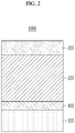
- FIG. 2 is a diagram illustrating the display device 1000 according to an exemplary embodiment of the present invention.
- the display device 1000 includes a cover window 300, a display panel 200, a base film 400, and the cushion layer 100.
- An adhesive layer may be disposed between the cover window 300 and the display panel 200, between the display panel 200 and the base film 400, and between the base film 400 and the cushion layer 100.
- the display device 1000 may be a flexible display device that is bendable.
- the flexible display device may either be a curved display device of which the display device is entirely curved with a predetermined curvature or a folded display device of which the display device is folded, such as folded in half.
- the cover window 300 may be made of a film. The cover window 300 protects the display panel 200.
- the display panel 200 may include a transistor and an electrode connected thereto.
- the display panel 200 may be a liquid crystal panel or a display panel including an organic light emitting element. However, other kinds of display panels 200 may alternatively be used.
- the display panel 200 may include a light-emitting element having a quantum dot or an inorganic material as an emission layer.
- a touch panel or a polarizer may be disposed between the cover window 300 and the display panel 200.
- the base film 400 may support the display panel 200 and may protect the display panel 200 from damage caused by an external impact. Also, the base film 400 may smooth the impact, dissipate heat of the display panel 200, and block light of the display panel 200. However, the base film 400 may be omitted according to an exemplary embodiment of the present disclosure.
- the cushion layer 100 smooths the impact applied to the display device 1000.
- the cushion layer 100 absorbs the impact applied at the upper part and the lower part of the display device 1000 so that the impact is not transmitted inside the display panel 200. Accordingly, damage to the display panel 200 may be prevented.
- the cushion layer 100 may have the high modulus. As the cushion layer 100 has the high modulus, the damage to the display panel 200 from the impact applied to the display device 1000 may be prevented.
- the display device 1000 is the flexible display device, and each layer of the flexible display device 1000 is bent.
- the cushion layer 100 includes the material having the high modulus
- the display device 1000 does not bend well, and cracks may be generated in the cushion layer 100 or other layers.
- the cushion layer 100 is formed of the material having the low modulus to allow the display device 1000 to bend well, impact might not be sufficiently absorbed due to the low modulus of the cushion layer 100. Accordingly, when the impact is applied to the display device 1000, the display panel 200 is damaged and a bright point or a dark point is generated.
- the bending characteristic of the cushion layer 100 and the impact resistance characteristic are in a trade-off relationship.
- the impact resistance characteristic is reduced such that the display panel 200 is susceptible to damage, and when using the material having the high modulus to increase the impact resistance characteristic, the bending characteristic is poor such that cracks are generated in the cushion layer 100.
- the cushion layer 100 includes the first member 10 and the second member 20 having the different moduli.
- the modulus of the first member 10 is high compared with that of the second member 20, and the first member 100 absorbs the impact.
- the second member 20 includes the material having the low modulus compared with the first member 10 such that the second member 20 bends well. Accordingly, the cushion layer 100 may have both of the bending characteristic and the impact resistance characteristic.
- the first member 10 having the high modulus includes the plurality of first grooves 11 and second grooves 12. When bending the cushion layer 100, the first grooves 11 and the second grooves 12 tend to extend or compress, and so the bending characteristic of the first member 10 is increased.
- the cushion layer 100 may have both the bending characteristic of the first grooves 11 and the second grooves 12 formed in the first member and the low modulus of the second member 20 while having the impact resistance characteristic of the first member 10 having the high modulus.
- the first member 10 may have the structure in which the cushion member 15 is compressed.
- FIG. 3 is a diagram illustrating the cushion member 15 before being processed in the first member 10 of the cushion layer 100.
- the cushion member 15 has a plurality of grooves 14.
- the maximum width h1 of the grooves 14 is wider than the maximum width d1 of the first grooves 11 and the maximum width d2 of the second grooves 12 of the first member 10 in FIG. 1 .
- the length L of the cushion member 15 is longer than the length of the first member 10 that is finally processed.
- the cushion member 15 is compressed to be processed into the first member 10 and the second member 20 is formed at the exterior of the first member 10, thereby manufacturing the cushion layer 100.
- the length of the first member 10 is 2/3L to 3/4L. This reduction in length is achieved by compressing the cushion member 15 in the length-wise direction.
- the first member 10 may be in a state in which the cushion member 15 is compressed by about 20 % to 40 %. Since the first member 10 is in the state in which the cushion member 15 is compressed, the tensile stress may be absorbed while the compressed part is expanded when bending the display device 1000.
- a ratio of the maximum width h1 of the grooves 14 and the minimum width h2 of the region where the groove is not formed may be 1:2 to 2:1. However, this is only an example, and other ratios may be used.
- FIG. 4 is a diagram illustrating the display device in the flat state
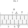
- FIG. 5 shows the cross-sectional view of the cushion layer 100 in FIG. 4
- the display device 1000 of FIG. 4 is schematically shown in the state of only including the cover window 300, the display panel 200, and the cushion layer 100.
- the maximum width d1 of the first grooves 11 of the cushion layer 100 and the maximum width d2 of the second grooves 12 are the same.
- FIG. 6 is a diagram illustrating a state in which the display device is bent
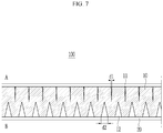
- FIG. 7 is a cross-sectional view of the cushion layer 100 when the display device is in the bent state of FIG. 6
- FIG. 7 is the cross-sectional view of the cushion layer 100 in the bending portion (indicated by a dotted line) in FIG. 6
- the compressed surface is indicated by A
- the tensioned surface is indicated by B.
- the first grooves 11 of a part A subjected to the compressive stress of the cushion layer 100 is compressed such that the maximum width d1 thereof decreases.
- the second grooves 12 disposed at a part B subjected to the tensile stress is tensioned such that the maximum width d2 thereof increases.
- the maximum width d1 of the first grooves and the maximum width d2 of the second grooves are the same, however referring to FIG. 7 , when the display panel is bent, the maximum width d2 of the second grooves is larger than the maximum width d1 of the first grooves.
- the cushion layer 100 may be easily bent, without cracking, despite having the high modulus.
- FIG. 8 to FIG. 27 are diagrams illustrating a structure of the cushion layer 100 according to exemplary embodiments of the present invention. Differences between the cushion layer 100 of these figures and the cushion layer 100 illustrated in FIG. 1 will be mainly described below and it is to be understood that details that are omitted with respect to these figures may be at least similar to corresponding details that have already been described with respect to FIG. 1 .
- FIG. 8 is a diagram illustrating the cushion layer 100 according to an exemplary embodiment of the present invention.
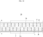
- the widths of the first grooves 11 and the second grooves 12 are different.
- the maximum width of a bent first grooves 11a disposed at the bending portion C is wider than the maximum width of the first grooves 11 that is not at the bending portion C.
- the maximum width of a bent second grooves 12a disposed at the bending portion C is narrower than the maximum width of the second grooves 12 of the region that is not the bending portion C.
- the region A subjected to the compressive stress may be compressed since the groove is wider, and the region B subjected to the tensioned stress may be tensioned since the groove is narrow. Accordingly, the cushion layer 100 may be effectively bent.
- the structure of FIG. 1 is suitable for the case that the bending direction of the display device is not specified, and even if the display device is bent in any direction, the compressive stress and the tensile stress may be offset.
- the bending direction of the display device is specified, as the grooves of the compressive direction are wider and the grooves of the tensile direction are narrower, the bending characteristic of the cushion layer 100 may be further increased.
- the maximum widths of the bent first grooves 11a and the first grooves 11 of the bending portion C are different and the maximum widths of the bent second groove 12a and the second grooves 12 are different, however only one of the first grooves 11 and the second grooves 12 may have the different width in the bending portion C.
- the maximum widths of the bent first groove 11a and the first grooves 11 are different and the maximum widths of the bent second groove 12a and the second grooves 12 are the same.
- the maximum widths of the bent second groove 12a and the second grooves 12 may be different and the bent first groove 11a and the first grooves 11 may be the same.
- FIG. 11 is a diagram illustrating a cushion layer 100 according to an exemplary embodiment of the present invention.
- the maximum width of the bent first groove 11a is gradually changed.
- the maximum width of the bent first groove 11a is widened closer to the center of the bending portion C. Since the bent first groove 11a is widest at the center part of the bending portion C to which the most compressive stress is applied during the bending, the compressive stress may be effectively absorbed.
- the maximum width of the bent second groove 12a decreases closer to the center from the edge of the bending portion C. Accordingly, compared with the structure of FIG. 8 , the compressive stress and the tensile stress may be further effectively absorbed.
- only the width of the bent first groove 11a may be gradually changed in FIG. 11 , and the bent second groove 12a may have the uniform width.
- only the width of the bent second groove 12a may be gradually changed in FIG. 11 , and the bent first groove 11a may have the uniform width.
- the width of the first grooves 11 and the width of the second grooves 12 may be gradually changed in the entire cushion layer 100.
- the maximum width of the first grooves 11 is gradually increased closer to the center from the edge of the cushion layer 100.
- the maximum width of the second grooves 12 is gradually decreased to the center from the edge of the cushion layer 100.
- the compressive stress applied in the region A and the tensile stress applied to the region B may be uniformly distributed in stages in the entire cushion layer 100.
- the maximum width of the first grooves 11 may be gradually increased closer to the center from the edge of the cushion layer 100, and the maximum width of the second grooves 12 may be the same in the entire cushion layer 100.
- the maximum width of the second grooves 12 is gradually decreased to the center from the edge of the cushion layer 100, and the maximum width of the first grooves 11 may be uniform in the entire cushion layer 100.
- first grooves 11 and the second grooves 12 are formed in the entire cushion layer 100, however the first grooves 11 and the second grooves 12 may only be formed in the bending portion C.
- FIG. 17 to FIG. 22 are similar to FIG. 8 to FIG. 16 , but show the cushion layer 100 in which only the first grooves 11 and the second grooves 12 are formed in the bending region.
- the first grooves 11 and the second grooves 12 are disposed at the bending portion C, and the groove is not disposed at the region that is not the bending portion C.
- the maximum width of the first grooves 11 of the region A where the cushion layer 100 is compressed is larger than the maximum width of the second grooves 12 of the region B where the cushion layer 100 is tensioned.
- only the first grooves 11 may be disposed in the bending portion C.
- only the second grooves 12 may be disposed in the bending portion C.
- the size of the first grooves 11 and the second grooves 12 of the bending portion C may be gradually changed.
- the size of the first grooves 11 may be increased closer to the center, and the size of the second grooves 12 may be decreased closer to the center.
- only the size of the first grooves 11 may be increased closer to the center, and the size of the second grooves 12 may be uniform.
- only the size of the second grooves 12 may be decreased closer to the center, and the size of the first grooves 11 may be uniform.
- the bending characteristic of the cushion layer 100 may be further increased.
- the cushion layer 100 includes a plurality of third grooves 13 disposed between the first grooves 11 in the bending portion C.
- the third grooves 13 may have a shorter length than the first grooves 11. Accordingly, the third grooves 13 do not meet the second grooves 12. However, the third grooves 13 may have the same length as the first grooves 11. As an auxiliary layer such as the third grooves 13 is disposed at the region A where the compressive stress is applied, the compressive stress may be effectively offset. For example, the compressive stress is offset while empty spaces due to the groove are reduced, and as more grooves are disposed at the region A where the compressive stress is applied compared with the region B where the tensile stress is applied, more compressive stress may be offset.
- FIG. 23 is a structure that may be used when the bending portion C is specified, and the structure of FIG. 24 may effectively offset the compressive-tensile stress no matter what part is bent when the bending portion C is not specified in the cushion layer.
- the first grooves 11, the second grooves 12, and the third grooves 13 may only be disposed in the bending portion, and the groove might not be disposed in the region that is not the bending portion C.
- FIG. 26 is a diagram illustrating the cushion layer 100, according to an exemplary embodiment of the present invention.
- the cycle of the first grooves 11 and the cycle of the second grooves 12 may be shorter closer to the center from the edge of the cushion layer 100.
- first grooves 11 and the second grooves 12 are densely formed at the center where most stress is concentrated during the bending, and are sparsely formed farther away from the center such that the compressive stress and the tensile stress may be effectively distributed.
- FIG. 27 is a diagram illustrating the cushion layer 100 according to an exemplary embodiment of the present invention.
- the first grooves 11 and the second grooves 12 are disposed in parallel.
- the first grooves 11 and the second grooves 12 are disposed to alternate with each other, however the first grooves 11 and the second grooves 12 are disposed in parallel on the same line in FIG. 27 .
- the structure in which the first grooves 11 and the second grooves 12 are changed to be in parallel like in FIG. 27 is included as an exemplary embodiment of the present invention.
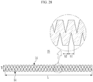
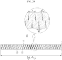
- FIG. 28 to FIG. 30 are process cross-sectional views showing a manufacturing process of a cushion layer 100 according to an exemplary embodiment of the present invention.
- the cushion member 15 in the state that it is not compressed is first prepared.
- the cushion member 15 has a plurality of grooves 14.
- the ratio of the maximum width h1 of the grooves 14 and the minimum width h2 of the region where the groove is not formed may be 1:2 to 2:1. However, this is only an example, and other ratios may be used. For example, the ratio of the region where the groove is formed and the region where the groove is not formed may be 1:1.
- the thickness Tc of the cushion member 15 may be within the range of 100 ⁇ m to 300 ⁇ m, inclusive.
- the cushion member 15 may include the material having the modulus within the range of 0.1 GPa to 1000 GPa, inclusive.
- the cushion member 15 may include polyethylene terephthalate (PET) and/or polyimide (PI), however other materials may be used.
- the interval and the size of the plurality of grooves 14 of the cushion member are constant, however the grooves 14 of FIG. 28 may be one among the various structures described in FIG. 1 to FIG. 27 .
- the cushion member 15 is compressed to form the first member 10.
- the compressed thickness in FIG. 29 may be 2/3L to 3/4L.
- the first member 10 may be in a state in which the cushion member 15 is compressed by about 20 % to 40 %.
- the first grooves 11 and the second grooves 12 having the smaller width than the grooves 14 of the cushion member 15 are formed.
- the maximum width d1 of the first groove or the maximum width d2 of the second groove may be within the range of 10 ⁇ m to 400 ⁇ m, inclusive.
- the cushion layer 100 might not absorb the impact of the display panel. This is because the empty space of the groove region does not absorb the impact when the impact is applied to the cushion layer 100 and the cushion layer 100 may be collapsed.
- the width is only an example, and the maximum width d1 of the first grooves 11 and the maximum width d2 of the second grooves 12 may be different from each other. Also, in the region of the cushion layer 100, the width of the groove may be gradually increased or differentiated, and may be different for each region.
- the cycle P of the first grooves 11 or the second grooves 12 may be within the range of 20 ⁇ m to 1000 ⁇ m, inclusive. However, this is only an example, and other cycles may be used. As above-described, the formation cycle of the first grooves 11 and the second grooves 12 may be different from each other and may be differentiated in the bending region.
- the second member 20 enclosing the first member 10 is formed.
- the second member 20 may include the material having the lower modulus than the first member 10.
- the modulus of the second member 20 may be within the range of 1 KPa to 1000 KPa, inclusive.
- the second member 20 includes the material having the low modulus, the bending characteristic is excellent. Accordingly, even if the display device including the cushion layer 100 is bent, the display device may be easily bent without cracking.
- the cushion layer 100 includes the first member 10 and the second member 20 having the different moduli, and the first member 10 includes the plurality of grooves.
- the impact resistance of the cushion layer 100 may be obtained by the first member 10 having the high modulus, and the excellent bending characteristic may be obtained through the absorption of the compress/tensile stress by the plurality of grooves included in the first member 10 and the second member 20 having the low modulus. Accordingly, when applying the cushion layer 100 to the curved display device, damage to the display panel may be prevented while still allowing for easy bending.
- the characterizing portion of claim 1 comprises features relating to the modulus of the first member and of the second member.
Landscapes
- Physics & Mathematics (AREA)
- Engineering & Computer Science (AREA)
- General Physics & Mathematics (AREA)
- Theoretical Computer Science (AREA)
- Nonlinear Science (AREA)
- Computer Hardware Design (AREA)
- Optics & Photonics (AREA)
- Crystallography & Structural Chemistry (AREA)
- Chemical & Material Sciences (AREA)
- Mathematical Physics (AREA)
- Human Computer Interaction (AREA)
- General Engineering & Computer Science (AREA)
- Manufacturing & Machinery (AREA)
- Devices For Indicating Variable Information By Combining Individual Elements (AREA)
Abstract
Description
- The present disclosure relates to a display device and, more specifically, to a display device including a cushion layer having members with different moduli.
- A display device is a device that displays an image. Examples of products incorporating display devices include a television, a computer monitor, a personal digital assistant (PDA), and Internet-connected devices, which may be referred to as "smart equipment" of which demand has recently increased.
- Display devices may use a flat type of display module with high display quality such as an organic light emitting panel, a liquid crystal panel, a plasma display panel, an electrophoretic display panel, etc.
- Recently, flexible display devices which may be light weight and thin have been developed. However, in the case of the flexible display device, because a thin substrate is used to achieve flexibility, the flexible display device is relatively susceptible to impact.
- A display device includes a cushion layer and a display panel disposed on a top surface of the cushion layer. The cushion layer includes a first member and a second member at least partially surrounding the first member. The first member includes a first material having a first modulus. The second member includes a second material having a second modulus that is smaller than the first modulus. The first member includes a plurality of grooves disposed therein.
- A flexible display device includes a cushion layer and a display panel disposed on a top surface of the cushion layer. The cushion layer includes a first member and a second member at least partially surrounding the first member. The first member includes a first material having a first modulus. The second member includes a second material having a second modulus that is smaller than the first modulus. The cushion layer includes a bending portion. The first member includes a plurality of grooves disposed in the bending portion.
- A method of manufacturing a display device includes preparing a cushion member including a plurality of grooves disposed therein. The cushion member is compressed to form a first member. A second member is formed to at least partially surrounding the first member. A modulus of the first member is larger than a modulus of the second member.
- A more complete appreciation of the present disclosure and many of the attendant aspects thereof will be readily obtained as the same becomes better understood by reference to the following detailed description when considered in connection with the accompanying drawings, wherein:
-
FIG. 1 is a diagram illustrating a cushion layer according to an exemplary embodiment of the present invention; -
FIG. 2 is a diagram illustrating a display device according to an exemplary embodiment of the present invention; -
FIG. 3 is a diagram illustrating a cushion member before a first member of a cushion layer is processed; -
FIG. 4 is a diagram illustrating a flat state of a display device; -
FIG. 5 is a cross-sectional diagram illustrating a cushion layer when a display device is in a flat state ofFIG. 4 ; -
FIG. 6 is a diagram illustrating a bent state of a display device; -
FIG. 7 is a cross-sectional diagram illustrating a cushion layer when a display device is in a bent state ofFIG. 6 ; -
FIG. 8 to FIG. 27 are diagrams illustrating a structure of a cushion layer according to exemplary embodiments of the present invention; and -
FIG. 28 to FIG. 30 are cross-sectional diagrams illustrating a manufacturing process of a cushion layer according to an exemplary embodiment of the present invention. - Exemplary embodiments of the present invention will be described more fully hereinafter with reference to the accompanying drawings. As those skilled in the art would realize, the described embodiments may be modified in various different ways, all without departing from the spirit or scope of the present invention.
- Like reference numerals may designate like elements throughout the specification and figures.
- Further, in the drawings, a size and thickness of each element may be exaggerated for better understanding and ease of description. In the drawings, the thickness of layers, films, panels, regions, etc., may be exaggerated for clarity.
- It will be understood that when an element such as a layer, film, region, or substrate is referred to as being "on" another element, it can be directly on the other element or intervening elements may also be present. Further, in the specification, the word "on" or "above" means arranged on or below the object portion, and does not necessarily mean arranged on the upper side of the object portion based on a gravitational direction.
- Exemplary embodiments of the present invention relate to a display device having a cushion layer included therein. An inner part and an outer part of the cushion layer may have different moduli. A plurality of grooves is formed in the cushion layer. As a result of the inclusion of the plurality of grooves, the cushion layer has excellent impact resistance and bending characteristics.
-
FIG. 1 shows acushion layer 100 according to an exemplary embodiment of the present invention. Referring toFIG. 1 , thecushion layer 100 includes afirst member 10 disposed therein and asecond member 20 at least partially enclosing an exterior of the first member. For example, thesecond member 20 is disposed outside thefirst member 10. - The
first member 10 includes a plurality offirst grooves 11 and a plurality ofsecond grooves 12. Referring toFIG. 1 , the plurality offirst grooves 11 and the plurality ofsecond grooves 12 of thefirst member 10 are arranged in the opposite directions to each other. For example, each of the plurality offirst grooves 11 may originate at a top surface of thefirst member 10 and point downward while each of the plurality ofsecond grooves 12 may originate at a bottom surface of thefirst member 10 and point upwards. Thus, opening of each of the first plurality ofgrooves 11 and an opening of each of the second plurality ofgrooves 12 are disposed at different surfaces of thefirst member 10. - Referring to
FIG. 1 , each of the first plurality of grooves 11 (the "first grooves") and each of the second plurality of grooves 12 (the "second grooves") may have a triangle shape. The plurality offirst grooves 11 and the plurality ofsecond grooves 12 may act to reduce a compressive stress or a tensile stress applied to thecushion layer 100 when bending thecushion layer 100 and may prevent a crack, etc. from forming in thecushion layer 100. - Referring to
FIG. 1 , thefirst grooves 11 and thesecond grooves 12 may be staggered from each other. For example, a center line of thefirst grooves 11 and a center line of thesecond grooves 12 do not meet each other. However, as an alternative, thefirst grooves 11 and thesecond grooves 12 may be arranged along the same center lines such that each of thefirst grooves 11 is aligned with each of thesecond grooves 12. - Referring to
FIG. 1 , a maximum width d1 of each of thefirst grooves 11 and/or a maximum width d2 of each of thesecond grooves 12 may be within the range of 10 µm to 400 µm, inclusive. When the maximum width d1 of each of thefirst grooves 11 and/or the maximum width d2 of each of thesecond grooves 12 is more than 400 µm, thecushion layer 100 might not absorb an impact applied to the display panel and may collapse. Also, when the maximum width d1 of thefirst grooves 11 or the maximum width d2 of thesecond grooves 12 is less than 10 µm, the area where the groove is compressed may be reduced such that the stress during compressive deformation might not be sufficiently absorbed. - According to an exemplary embodiment of the present invention, the
first member 10 may include a material having higher modulus than that of thesecond member 20. The modulus of thefirst member 10 may be larger than that of thesecond member 20 by 10 times to 10,000 times. For example, the modulus of thefirst member 10 may be 0.1 GPa to 1000 GPa, and the modulus of thesecond member 20 may be 1 KPa to 1000 KPa. - The first member may include polyethylene terephthalate (PET) and/or polyimide (PI). However, the material of the first member is not limited thereto. A formation cycle P of the
first grooves 11 or thesecond grooves 12 may be within the range of 20 µm to 1000 µm, inclusive. However, this is only an example, and the formation cycle is not limited thereto. Also, a thickness "t" of thecushion layer 100 may be within the range of 100 µm to 400 µm, inclusive. However, this is only an example, and the formation cycle is not limited thereto. - When the
first member 10 disposed inside thecushion layer 100 and including the grooves is formed of the material having a high modulus and thesecond member 20 is formed of the material having the modulus that is lower than that of the first member 10 (the "low modulus"), the impact resistance and the bending characteristic of thecushion layer 100 may both be increased. The impact resistance and the bending characteristic might not be compatible physical properties for a single material, however as shown herein, the impact resistance and the bending characteristic may be realized by thegrooves first member 10 having the high modulus and thesecond member 20 having the low modulus. - An effect of the
cushion layer 100 on thedisplay device 1000 according to an exemplary embodiment of the present invention is described. - The above used term "first member" might also be called "cover" or "skin". Its function is to envelope the "second member". The first member may consist of any flexible material which allows to be bent or folded.
- The above used term "groove" may have cross section of a wedge as shown in the figures. But it may be of cross section different therefrom, e.g. any cutout which is open at the other surface of the second member, and extending into the same to a certain extent.
-
FIG. 2 is a diagram illustrating thedisplay device 1000 according to an exemplary embodiment of the present invention. Referring toFIG. 2 , thedisplay device 1000, according to an exemplary embodiment of the present invention, includes acover window 300, adisplay panel 200, abase film 400, and thecushion layer 100. An adhesive layer may be disposed between thecover window 300 and thedisplay panel 200, between thedisplay panel 200 and thebase film 400, and between thebase film 400 and thecushion layer 100. - The
display device 1000, according to an exemplary embodiment of the present invention, may be a flexible display device that is bendable. The flexible display device may either be a curved display device of which the display device is entirely curved with a predetermined curvature or a folded display device of which the display device is folded, such as folded in half. When thedisplay device 1000 is the flexible display device, thecover window 300 may be made of a film. Thecover window 300 protects thedisplay panel 200. - The
display panel 200 may include a transistor and an electrode connected thereto. Thedisplay panel 200 may be a liquid crystal panel or a display panel including an organic light emitting element. However, other kinds ofdisplay panels 200 may alternatively be used. Thedisplay panel 200 may include a light-emitting element having a quantum dot or an inorganic material as an emission layer. - A touch panel or a polarizer may be disposed between the
cover window 300 and thedisplay panel 200. - The
base film 400 may support thedisplay panel 200 and may protect thedisplay panel 200 from damage caused by an external impact. Also, thebase film 400 may smooth the impact, dissipate heat of thedisplay panel 200, and block light of thedisplay panel 200. However, thebase film 400 may be omitted according to an exemplary embodiment of the present disclosure. - The
cushion layer 100 smooths the impact applied to thedisplay device 1000. Thecushion layer 100 absorbs the impact applied at the upper part and the lower part of thedisplay device 1000 so that the impact is not transmitted inside thedisplay panel 200. Accordingly, damage to thedisplay panel 200 may be prevented. - To prevent the damage to the
display panel 200 and absorb the impact, thecushion layer 100 may have the high modulus. As thecushion layer 100 has the high modulus, the damage to thedisplay panel 200 from the impact applied to thedisplay device 1000 may be prevented. - The
display device 1000, according to an exemplary embodiment of the present invention, is the flexible display device, and each layer of theflexible display device 1000 is bent. However, when thecushion layer 100 includes the material having the high modulus, thedisplay device 1000 does not bend well, and cracks may be generated in thecushion layer 100 or other layers. Also, when thecushion layer 100 is formed of the material having the low modulus to allow thedisplay device 1000 to bend well, impact might not be sufficiently absorbed due to the low modulus of thecushion layer 100. Accordingly, when the impact is applied to thedisplay device 1000, thedisplay panel 200 is damaged and a bright point or a dark point is generated. - Thus, in the
flexible display device 1000, the bending characteristic of thecushion layer 100 and the impact resistance characteristic are in a trade-off relationship. When using the material having the low modulus to allow for bending, the impact resistance characteristic is reduced such that thedisplay panel 200 is susceptible to damage, and when using the material having the high modulus to increase the impact resistance characteristic, the bending characteristic is poor such that cracks are generated in thecushion layer 100. - However, the
cushion layer 100, according to exemplary embodiments of the present inventio, includes thefirst member 10 and thesecond member 20 having the different moduli. The modulus of thefirst member 10 is high compared with that of thesecond member 20, and thefirst member 100 absorbs the impact. Thesecond member 20 includes the material having the low modulus compared with thefirst member 10 such that thesecond member 20 bends well. Accordingly, thecushion layer 100 may have both of the bending characteristic and the impact resistance characteristic. Also, thefirst member 10 having the high modulus includes the plurality offirst grooves 11 andsecond grooves 12. When bending thecushion layer 100, thefirst grooves 11 and thesecond grooves 12 tend to extend or compress, and so the bending characteristic of thefirst member 10 is increased. - For example, the
cushion layer 100, according to an exemplary embodiment of the present disclosure, may have both the bending characteristic of thefirst grooves 11 and thesecond grooves 12 formed in the first member and the low modulus of thesecond member 20 while having the impact resistance characteristic of thefirst member 10 having the high modulus. - The
first member 10 may have the structure in which thecushion member 15 is compressed.FIG. 3 is a diagram illustrating thecushion member 15 before being processed in thefirst member 10 of thecushion layer 100. Referring toFIG. 3 , thecushion member 15 has a plurality ofgrooves 14. In this case, the maximum width h1 of thegrooves 14 is wider than the maximum width d1 of thefirst grooves 11 and the maximum width d2 of thesecond grooves 12 of thefirst member 10 inFIG. 1 . Also, the length L of thecushion member 15 is longer than the length of thefirst member 10 that is finally processed. Thecushion member 15 is compressed to be processed into thefirst member 10 and thesecond member 20 is formed at the exterior of thefirst member 10, thereby manufacturing thecushion layer 100. When the length of thecushion member 15 is L, the length of thefirst member 10 is 2/3L to 3/4L. This reduction in length is achieved by compressing thecushion member 15 in the length-wise direction. For example, thefirst member 10 may be in a state in which thecushion member 15 is compressed by about 20 % to 40 %. Since thefirst member 10 is in the state in which thecushion member 15 is compressed, the tensile stress may be absorbed while the compressed part is expanded when bending thedisplay device 1000. - In the
cushion member 15 before compression, a ratio of the maximum width h1 of thegrooves 14 and the minimum width h2 of the region where the groove is not formed may be 1:2 to 2:1. However, this is only an example, and other ratios may be used. -
FIG. 4 is a diagram illustrating the display device in the flat state, andFIG. 5 shows the cross-sectional view of thecushion layer 100 inFIG. 4 . Thedisplay device 1000 ofFIG. 4 is schematically shown in the state of only including thecover window 300, thedisplay panel 200, and thecushion layer 100. Referring toFIG. 5 , when the display device is flat without being bent, the maximum width d1 of thefirst grooves 11 of thecushion layer 100 and the maximum width d2 of thesecond grooves 12 are the same. -
FIG. 6 is a diagram illustrating a state in which the display device is bent, andFIG. 7 is a cross-sectional view of thecushion layer 100 when the display device is in the bent state ofFIG. 6 .FIG. 7 is the cross-sectional view of thecushion layer 100 in the bending portion (indicated by a dotted line) inFIG. 6 . InFIG. 6 andFIG. 7 , when the display device is bent, the compressed surface is indicated by A and the tensioned surface is indicated by B. - Referring to
FIG. 7 , when the display panel is bent, thefirst grooves 11 of a part A subjected to the compressive stress of thecushion layer 100 is compressed such that the maximum width d1 thereof decreases. In contrast, thesecond grooves 12 disposed at a part B subjected to the tensile stress is tensioned such that the maximum width d2 thereof increases. - Referring to
FIG. 5 , when the display panel is flat, the maximum width d1 of the first grooves and the maximum width d2 of the second grooves are the same, however referring toFIG. 7 , when the display panel is bent, the maximum width d2 of the second grooves is larger than the maximum width d1 of the first grooves. - As described above, as the width of the groove of the part subjected to the compressive stress decreases and the width of the groove of the part subjected to the tensioned stress increases, the
cushion layer 100, according to an exemplary embodiment of the present invention, may be easily bent, without cracking, despite having the high modulus. - Next, the
cushion layer 100, according to an exemplary embodiment of the present invention, is described.FIG. 8 to FIG. 27 are diagrams illustrating a structure of thecushion layer 100 according to exemplary embodiments of the present invention. Differences between thecushion layer 100 of these figures and thecushion layer 100 illustrated inFIG. 1 will be mainly described below and it is to be understood that details that are omitted with respect to these figures may be at least similar to corresponding details that have already been described with respect toFIG. 1 . -
FIG. 8 is a diagram illustrating thecushion layer 100 according to an exemplary embodiment of the present invention. Referring toFIG. 8 , in the bending portion C, where the display device is bent, the widths of thefirst grooves 11 and thesecond grooves 12 are different. The maximum width of a bentfirst grooves 11a disposed at the bending portion C is wider than the maximum width of thefirst grooves 11 that is not at the bending portion C. In contrast, the maximum width of a bentsecond grooves 12a disposed at the bending portion C is narrower than the maximum width of thesecond grooves 12 of the region that is not the bending portion C. According to an exemplary embodiment of the present disclosure, when the display device is bent or folded, the region A subjected to the compressive stress may be compressed since the groove is wider, and the region B subjected to the tensioned stress may be tensioned since the groove is narrow. Accordingly, thecushion layer 100 may be effectively bent. The structure ofFIG. 1 is suitable for the case that the bending direction of the display device is not specified, and even if the display device is bent in any direction, the compressive stress and the tensile stress may be offset. However, in the structure ofFIG. 8 , when the bending direction of the display device is specified, as the grooves of the compressive direction are wider and the grooves of the tensile direction are narrower, the bending characteristic of thecushion layer 100 may be further increased. - In
FIG. 8 , the maximum widths of the bentfirst grooves 11a and thefirst grooves 11 of the bending portion C are different and the maximum widths of the bentsecond groove 12a and thesecond grooves 12 are different, however only one of thefirst grooves 11 and thesecond grooves 12 may have the different width in the bending portion C. Referring toFIG. 9 , the maximum widths of the bentfirst groove 11a and thefirst grooves 11 are different and the maximum widths of the bentsecond groove 12a and thesecond grooves 12 are the same. Also, referring toFIG. 10 , the maximum widths of the bentsecond groove 12a and thesecond grooves 12 may be different and the bentfirst groove 11a and thefirst grooves 11 may be the same. - Further, a size of the groove may be controlled depending a degree of compressive stress applied.
FIG. 11 is a diagram illustrating acushion layer 100 according to an exemplary embodiment of the present invention. Referring toFIG. 11 , in the bending portion C, the maximum width of the bentfirst groove 11a is gradually changed. For example, the maximum width of the bentfirst groove 11a is widened closer to the center of the bending portion C. Since the bentfirst groove 11a is widest at the center part of the bending portion C to which the most compressive stress is applied during the bending, the compressive stress may be effectively absorbed. This is the same in the case of the bentsecond groove 12a. For example, the maximum width of the bentsecond groove 12a decreases closer to the center from the edge of the bending portion C. Accordingly, compared with the structure ofFIG. 8 , the compressive stress and the tensile stress may be further effectively absorbed. - Referring to
FIG. 12 , only the width of the bentfirst groove 11a may be gradually changed inFIG. 11 , and the bentsecond groove 12a may have the uniform width. Also, referringFIG. 13 , only the width of the bentsecond groove 12a may be gradually changed inFIG. 11 , and the bentfirst groove 11a may have the uniform width. - Further, in an exemplary embodiment of the present invention, the width of the
first grooves 11 and the width of thesecond grooves 12 may be gradually changed in theentire cushion layer 100. Referring toFIG. 14 , the maximum width of thefirst grooves 11 is gradually increased closer to the center from the edge of thecushion layer 100. Also, the maximum width of thesecond grooves 12 is gradually decreased to the center from the edge of thecushion layer 100. In this case, the compressive stress applied in the region A and the tensile stress applied to the region B may be uniformly distributed in stages in theentire cushion layer 100. - Referring to
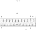
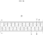
FIG. 15 , the maximum width of thefirst grooves 11 may be gradually increased closer to the center from the edge of thecushion layer 100, and the maximum width of thesecond grooves 12 may be the same in theentire cushion layer 100. Referring toFIG. 16 , the maximum width of thesecond grooves 12 is gradually decreased to the center from the edge of thecushion layer 100, and the maximum width of thefirst grooves 11 may be uniform in theentire cushion layer 100. - In the above, it is described based on the structure in which the
first grooves 11 and thesecond grooves 12 are formed in theentire cushion layer 100, however thefirst grooves 11 and thesecond grooves 12 may only be formed in the bending portion C. -
FIG. 17 to FIG. 22 are similar toFIG. 8 to FIG. 16 , but show thecushion layer 100 in which only thefirst grooves 11 and thesecond grooves 12 are formed in the bending region. - Referring to
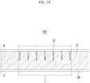
FIG. 17 , thefirst grooves 11 and thesecond grooves 12 are disposed at the bending portion C, and the groove is not disposed at the region that is not the bending portion C. The maximum width of thefirst grooves 11 of the region A where thecushion layer 100 is compressed is larger than the maximum width of thesecond grooves 12 of the region B where thecushion layer 100 is tensioned. Referring toFIG. 18 , only thefirst grooves 11 may be disposed in the bending portion C. Also, referring toFIG. 19 , only thesecond grooves 12 may be disposed in the bending portion C. - Referring to
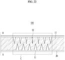
FIG. 20 , the size of thefirst grooves 11 and thesecond grooves 12 of the bending portion C may be gradually changed. The size of thefirst grooves 11 may be increased closer to the center, and the size of thesecond grooves 12 may be decreased closer to the center. Also, referring toFIG. 21 , only the size of thefirst grooves 11 may be increased closer to the center, and the size of thesecond grooves 12 may be uniform. Further, referring toFIG. 22 , only the size of thesecond grooves 12 may be decreased closer to the center, and the size of thefirst grooves 11 may be uniform. - When the sizes of the grooves are differentiated in the region A where the compressive stress is applied and the region B where the tensile stress is applied and the size of the groove is gradually changed depending on the magnitude of the stress in the same region, the bending characteristic of the
cushion layer 100 may be further increased. - Next, the
cushion layer 100, according to an exemplary embodiment of the present invention, is described. Referring toFIG. 23 , thecushion layer 100, according to an exemplary embodiment of the present disclosure, includes a plurality ofthird grooves 13 disposed between thefirst grooves 11 in the bending portion C. - The
third grooves 13 may have a shorter length than thefirst grooves 11. Accordingly, thethird grooves 13 do not meet thesecond grooves 12. However, thethird grooves 13 may have the same length as thefirst grooves 11. As an auxiliary layer such as thethird grooves 13 is disposed at the region A where the compressive stress is applied, the compressive stress may be effectively offset. For example, the compressive stress is offset while empty spaces due to the groove are reduced, and as more grooves are disposed at the region A where the compressive stress is applied compared with the region B where the tensile stress is applied, more compressive stress may be offset. - In
FIG. 23 , thethird grooves 13 are only disposed in the bending portion C, however as shown inFIG. 24 , thethird grooves 13 may be disposed in theentire cushion layer 100.FIG. 23 is a structure that may be used when the bending portion C is specified, and the structure ofFIG. 24 may effectively offset the compressive-tensile stress no matter what part is bent when the bending portion C is not specified in the cushion layer. - Also, as shown in
FIG. 25 , thefirst grooves 11, thesecond grooves 12, and thethird grooves 13 may only be disposed in the bending portion, and the groove might not be disposed in the region that is not the bending portion C. -
FIG. 26 is a diagram illustrating thecushion layer 100, according to an exemplary embodiment of the present invention. Referring toFIG. 26 , in thecushion layer 100, according to an exemplary embodiment of the present disclosure, the cycle of thefirst grooves 11 and the cycle of thesecond grooves 12 may be shorter closer to the center from the edge of thecushion layer 100. - For example, the
first grooves 11 and thesecond grooves 12 are densely formed at the center where most stress is concentrated during the bending, and are sparsely formed farther away from the center such that the compressive stress and the tensile stress may be effectively distributed. -
FIG. 27 is a diagram illustrating thecushion layer 100 according to an exemplary embodiment of the present invention. Referring toFIG. 27 , thefirst grooves 11 and thesecond grooves 12 are disposed in parallel. For example, inFIG. 1 to FIG. 26 , thefirst grooves 11 and thesecond grooves 12 are disposed to alternate with each other, however thefirst grooves 11 and thesecond grooves 12 are disposed in parallel on the same line inFIG. 27 . In the above-described structure ofFIG. 1 to FIG. 26 , the structure in which thefirst grooves 11 and thesecond grooves 12 are changed to be in parallel like inFIG. 27 is included as an exemplary embodiment of the present invention. - Next, a manufacturing method of the
cushion layer 100 according to an exemplary embodiment of the present invention is described. -
FIG. 28 to FIG. 30 are process cross-sectional views showing a manufacturing process of acushion layer 100 according to an exemplary embodiment of the present invention. - Referring to
FIG. 28 , thecushion member 15 in the state that it is not compressed is first prepared. - The
cushion member 15 has a plurality ofgrooves 14. In thecushion member 15, the ratio of the maximum width h1 of thegrooves 14 and the minimum width h2 of the region where the groove is not formed may be 1:2 to 2:1. However, this is only an example, and other ratios may be used. For example, the ratio of the region where the groove is formed and the region where the groove is not formed may be 1:1. - The thickness Tc of the
cushion member 15 may be within the range of 100 µm to 300 µm, inclusive. Thecushion member 15 may include the material having the modulus within the range of 0.1 GPa to 1000 GPa, inclusive. Thecushion member 15 may include polyethylene terephthalate (PET) and/or polyimide (PI), however other materials may be used. - In
FIG. 28 , the interval and the size of the plurality ofgrooves 14 of the cushion member are constant, however thegrooves 14 ofFIG. 28 may be one among the various structures described inFIG. 1 to FIG. 27 . - Next, referring to
FIG. 29 , thecushion member 15 is compressed to form thefirst member 10. InFIG. 28 , when the length of thecushion member 15 is referred to as L, the compressed thickness inFIG. 29 may be 2/3L to 3/4L. For example, thefirst member 10 may be in a state in which thecushion member 15 is compressed by about 20 % to 40 %. By the compression, thefirst grooves 11 and thesecond grooves 12 having the smaller width than thegrooves 14 of thecushion member 15 are formed. - In this case, the maximum width d1 of the first groove or the maximum width d2 of the second groove may be within the range of 10 µm to 400 µm, inclusive. When the maximum width d1 of the first groove or the maximum width d2 of the second groove is more than 400 µm, the
cushion layer 100 might not absorb the impact of the display panel. This is because the empty space of the groove region does not absorb the impact when the impact is applied to thecushion layer 100 and thecushion layer 100 may be collapsed. - However, the width is only an example, and the maximum width d1 of the
first grooves 11 and the maximum width d2 of thesecond grooves 12 may be different from each other. Also, in the region of thecushion layer 100, the width of the groove may be gradually increased or differentiated, and may be different for each region. - Also, the cycle P of the
first grooves 11 or thesecond grooves 12 may be within the range of 20 µm to 1000 µm, inclusive. However, this is only an example, and other cycles may be used. As above-described, the formation cycle of thefirst grooves 11 and thesecond grooves 12 may be different from each other and may be differentiated in the bending region. - Next, referring to
FIG. 30 , thesecond member 20 enclosing thefirst member 10 is formed. Thesecond member 20 may include the material having the lower modulus than thefirst member 10. For example, the modulus of thesecond member 20 may be within the range of 1 KPa to 1000 KPa, inclusive. - Since the
second member 20 includes the material having the low modulus, the bending characteristic is excellent. Accordingly, even if the display device including thecushion layer 100 is bent, the display device may be easily bent without cracking. - As above-described, the
cushion layer 100, according to an exemplary embodiment of the present invention, includes thefirst member 10 and thesecond member 20 having the different moduli, and thefirst member 10 includes the plurality of grooves. The impact resistance of thecushion layer 100 may be obtained by thefirst member 10 having the high modulus, and the excellent bending characteristic may be obtained through the absorption of the compress/tensile stress by the plurality of grooves included in thefirst member 10 and thesecond member 20 having the low modulus. Accordingly, when applying thecushion layer 100 to the curved display device, damage to the display panel may be prevented while still allowing for easy bending. - Exemplary embodiments described herein are illustrative, and many variations can be introduced without departing from the spirit of the disclosure or from the scope of the appended claims. For example, elements and/or features of different exemplary embodiments may be combined with each other and/or substituted for each other within the scope of this disclosure and appended claims.
- The characterizing portion of
claim 1 comprises features relating to the modulus of the first member and of the second member. - It may be, however, consider to use a display device as per the preamble of
claim 1. - The preamble of
claim 1, however, instead the features of the characterizing portion thereof or in addition to this could comprise the features directed to the grooves of at least one of claims 2 to 15.
Claims (16)
- A display device (1000) comprising:a cushion layer (100);a display panel (200) disposed on a top surface of the cushion layer (100),the cushion layer (100) includes a first member (10) and a second member (20) at least partially surrounding the first member (10),characterized by the following features:the first member (10) includes a first material having a first modulus,wherein the second member (20) includes a second material having a second modulus that is smaller than the first modulus, andwherein the first member (10) includes a plurality of grooves (11, 12) disposed therein.
- The display device (1000) of claim 1, wherein the second member (20) covers at least a top surface and a bottom surface of the first member (10) and the plurality of grooves (11, 12) are included on both the top surface and the bottom surface of the first member (10).
- The display device (1000) of at least one of claims 1 or 2, wherein the first modulus is within a range of 0.1 GPa to 1000 GPa, inclusive and the second modulus is within a range of 1 KPa to 1000 KPa, inclusive.
- The display device (1000) of at least one of claims 1 to 3, wherein the first member (10) includes polyethylene terephthalate and/or polyimide.
- The display device (1000) of at least one of claims 1 to 4, wherein a cycle/interval (P) at which the plurality of grooves (11, 12) are arranged is within a range of 20 µm to 1000 µm, inclusive.
- The display device (1000) of at least one of claims 1 to 5, wherein a maximum width (d1, s2) of each of the plurality of grooves (11, 12) is within a range of 10 µm to 400 µm, inclusive.
- The display device (1000) of at least one of claims 1 to 6, wherein the plurality of grooves (11,12) includes a plurality of first grooves (11) disposed within the top surface of the first member (10) and arranged so as to point towards the bottom surface of the first member (10) and a plurality of second grooves (12) disposed within the bottom surface of the first member (10) and arranged so as to point towards the top surface of the first member (10).
- The display device (1000) of claim 7, wherein a maximum width (d1) of each of the plurality of first grooves (11) is smaller than a maximum width (d2) of at least some of the plurality of second grooves (12).
- The display device (1000) of claim 7 or 8,
wherein the cushion layer (100) includes a bending portion (C), and
wherein a maximum width (d2) of each of the plurality of second grooves (12) in the bending portion (C) is larger than a maximum width of each of the plurality of second grooves (12) not in the bending portion (C). - The display device of claim 7 or 8,
wherein the cushion layer (100) includes a bending portion (C), and
wherein the maximum width (d1) of each of the plurality of first grooves (11) in the bending portion (C) is smaller than a maximum width of each of the plurality of first grooves (11) not in the bending portion (C). - The display device (1000) of claim 10, wherein the maximum width (d2) of each of the plurality of second grooves (12) in the bending portion (C) is larger than a maximum width of each of the plurality of second grooves (12) not in the bending portion (C).
- The display device (1000) of at least one of claims 7 to 11,
wherein the cushion layer (100) includes a bending portion (C), and
wherein the maximum width of each of the plurality of second grooves (12) in the bending portion (C) is gradually increased closer to a center of the bending portion (C). - The display device (1000) of at least one of claims 7 to 11,
wherein the cushion layer (100) includes a bending portion (C), and
wherein the maximum width of each of the plurality of first grooves (11) in the bending portion (C) is gradually decreased closer to a center of the bending portion (C). - The display device (1000) of claim 13, wherein the maximum width of each of the plurality of second grooves (12) in the bending portion (C) is gradually increased closer to a center of the bending portion (C).
- The display device (1000) of at least one of claims 7 to 14, wherein the maximum width of each of the plurality of second grooves (12) is gradually increased closer to the center of the cushion layer (100).
- A display device (1000) comprising:a cushion layer (100);a display panel (200) disposed on a top surface of the cushion layer (100),the cushion layer (100) includes a first member (10) and a second member (20) at least partially surrounding the first member (10);characterized by at least one of claims 2 to 15
Applications Claiming Priority (1)
| Application Number | Priority Date | Filing Date | Title |
|---|---|---|---|
| KR1020180018513A KR102554240B1 (en) | 2018-02-14 | 2018-02-14 | Display device and manufacturing method thereof |
Publications (2)
| Publication Number | Publication Date |
|---|---|
| EP3528040A1 true EP3528040A1 (en) | 2019-08-21 |
| EP3528040B1 EP3528040B1 (en) | 2023-08-30 |
Family
ID=65440812
Family Applications (1)
| Application Number | Title | Priority Date | Filing Date |
|---|---|---|---|
| EP19157069.6A Active EP3528040B1 (en) | 2018-02-14 | 2019-02-14 | Display device including a cushion layer having members with different moduli |
Country Status (4)
| Country | Link |
|---|---|
| US (1) | US10936012B2 (en) |
| EP (1) | EP3528040B1 (en) |
| KR (1) | KR102554240B1 (en) |
| CN (1) | CN110164305A (en) |
Families Citing this family (17)
| Publication number | Priority date | Publication date | Assignee | Title |
|---|---|---|---|---|
| US11081660B2 (en) * | 2018-05-03 | 2021-08-03 | Samsung Display Co., Ltd. | Display device and support film structure for display device |
| WO2021029568A1 (en) * | 2019-08-13 | 2021-02-18 | 엘지이노텍 주식회사 | Substrate for display |
| CN110635014B (en) * | 2019-09-25 | 2022-01-25 | 昆山工研院新型平板显示技术中心有限公司 | Flexible cover plate and display panel |
| KR102727809B1 (en) | 2019-12-10 | 2024-11-07 | 엘지디스플레이 주식회사 | Foldable display device |
| KR20210096725A (en) * | 2020-01-28 | 2021-08-06 | 삼성디스플레이 주식회사 | Foldable display device |
| KR20220032831A (en) | 2020-09-08 | 2022-03-15 | 엘지디스플레이 주식회사 | Display device |
| CN112086571A (en) * | 2020-09-09 | 2020-12-15 | 武汉华星光电半导体显示技术有限公司 | Flexible display module |
| CN112164318B (en) * | 2020-10-14 | 2021-09-03 | 武汉华星光电半导体显示技术有限公司 | Support piece and foldable display module |
| KR20220068304A (en) | 2020-11-18 | 2022-05-26 | 삼성디스플레이 주식회사 | Electronic device |
| KR102847230B1 (en) * | 2021-05-24 | 2025-08-18 | 삼성디스플레이 주식회사 | cover window, manufacturing method of cover window, and display device including cover window |
| CN113516918B (en) | 2021-06-09 | 2022-04-29 | 荣耀终端有限公司 | A laminated display module and electronic equipment |
| KR20230067758A (en) * | 2021-11-08 | 2023-05-17 | 삼성디스플레이 주식회사 | Display device |
| KR20230094226A (en) * | 2021-12-20 | 2023-06-28 | 삼성디스플레이 주식회사 | Display device |
| JP2023094508A (en) * | 2021-12-23 | 2023-07-05 | パナソニックIpマネジメント株式会社 | Display device and input device |
| CN114360386B (en) * | 2022-01-28 | 2024-05-14 | 合肥维信诺科技有限公司 | Flexible cover plate and display device |
| CN114927061A (en) * | 2022-05-23 | 2022-08-19 | 武汉华星光电技术有限公司 | Manufacturing method of flexible cover plate and flexible cover plate |
| CN120183293A (en) * | 2025-04-29 | 2025-06-20 | 合肥维信诺科技有限公司 | Display panel cover and display screen |
Citations (3)
| Publication number | Priority date | Publication date | Assignee | Title |
|---|---|---|---|---|
| US20080042940A1 (en) * | 2006-08-21 | 2008-02-21 | Fujifilm Corporation | Display device |
| US20150195936A1 (en) * | 2014-01-07 | 2015-07-09 | Samsung Display Co., Ltd. | Window panel and display device including the same |
| US20170064845A1 (en) * | 2015-08-27 | 2017-03-02 | Samsung Display Co., Ltd. | Cover window of flexible display device and flexible display device having the same |
Family Cites Families (23)
| Publication number | Priority date | Publication date | Assignee | Title |
|---|---|---|---|---|
| TWI302821B (en) * | 2005-08-18 | 2008-11-01 | Ind Tech Res Inst | Flexible circuit board with heat sink |
| KR101925772B1 (en) * | 2008-07-10 | 2018-12-06 | 가부시키가이샤 한도오따이 에네루기 켄큐쇼 | Light emitting device and electronic device |
| KR20130060885A (en) * | 2011-11-30 | 2013-06-10 | 삼성디스플레이 주식회사 | Cushion sheet and display device having the same |
| KR101954983B1 (en) | 2012-08-09 | 2019-03-08 | 삼성디스플레이 주식회사 | Flexible display apparatus and the method for manufacturing the same |
| KR102057612B1 (en) * | 2013-05-21 | 2019-12-20 | 삼성디스플레이 주식회사 | Organic light emitting device and manufacturing method thereof |
| US9539757B2 (en) | 2013-06-26 | 2017-01-10 | Tekni-Plex, Inc. | Packing tray having cell pockets with expandable sidewalls and floating base, and method of manufacture |
| KR102056314B1 (en) * | 2013-09-27 | 2019-12-17 | 삼성디스플레이 주식회사 | Protective window and flexible display device including the same |
| KR102111726B1 (en) | 2013-10-30 | 2020-05-18 | 삼성디스플레이 주식회사 | Display device |
| KR20160103083A (en) * | 2013-12-24 | 2016-08-31 | 폴리에라 코퍼레이션 | Support structures for an attachable, two-dimensional flexible electronic device |
| KR102454065B1 (en) * | 2014-07-08 | 2022-10-17 | 삼성디스플레이 주식회사 | Foldable display device |
| TWI733654B (en) | 2014-11-04 | 2021-07-21 | 美商康寧公司 | Bendable glass articles with alkali-free glass elements |
| CN107108343B (en) | 2014-11-05 | 2020-10-02 | 康宁股份有限公司 | Glass articles with non-planar features and alkali-free glass elements |
| KR102345978B1 (en) | 2015-01-16 | 2021-12-31 | 삼성디스플레이 주식회사 | Organic light emitting diode display |
| US9983424B2 (en) * | 2015-06-08 | 2018-05-29 | Lg Display Co., Ltd. | Foldable display device |
| DE102016121942B4 (en) | 2015-11-30 | 2024-07-25 | Lg Display Co., Ltd. | Foldable display device |
| US10132478B2 (en) * | 2016-03-06 | 2018-11-20 | Svv Technology Innovations, Inc. | Flexible solid-state illumination devices |
| KR102559837B1 (en) * | 2016-06-02 | 2023-07-27 | 삼성디스플레이 주식회사 | Display apparatus |
| KR102717104B1 (en) * | 2016-09-27 | 2024-10-16 | 삼성디스플레이 주식회사 | Display apparatus and method for manufacturing the same |
| CN109845400B (en) * | 2016-10-13 | 2021-10-22 | 夏普株式会社 | Organic EL display device and manufacturing method of organic EL display device |
| JP6744203B2 (en) * | 2016-12-14 | 2020-08-19 | 株式会社ジャパンディスプレイ | Display device |
| CN106652802B (en) * | 2017-02-27 | 2020-03-17 | 上海天马微电子有限公司 | Foldable display device |
| CN107564415B (en) * | 2017-08-28 | 2019-06-21 | 上海天马有机发光显示技术有限公司 | Flexible display panel, display device and manufacturing method thereof |
| CN107578707B (en) * | 2017-10-20 | 2019-09-27 | 上海天马微电子有限公司 | Flexible display panel and display device |
-
2018
- 2018-02-14 KR KR1020180018513A patent/KR102554240B1/en active Active
-
2019
- 2019-01-18 US US16/252,033 patent/US10936012B2/en active Active
- 2019-02-14 CN CN201910113676.4A patent/CN110164305A/en active Pending
- 2019-02-14 EP EP19157069.6A patent/EP3528040B1/en active Active
Patent Citations (3)
| Publication number | Priority date | Publication date | Assignee | Title |
|---|---|---|---|---|
| US20080042940A1 (en) * | 2006-08-21 | 2008-02-21 | Fujifilm Corporation | Display device |
| US20150195936A1 (en) * | 2014-01-07 | 2015-07-09 | Samsung Display Co., Ltd. | Window panel and display device including the same |
| US20170064845A1 (en) * | 2015-08-27 | 2017-03-02 | Samsung Display Co., Ltd. | Cover window of flexible display device and flexible display device having the same |
Also Published As
| Publication number | Publication date |
|---|---|
| KR102554240B1 (en) | 2023-07-11 |
| KR20190098888A (en) | 2019-08-23 |
| EP3528040B1 (en) | 2023-08-30 |
| US20190250665A1 (en) | 2019-08-15 |
| US10936012B2 (en) | 2021-03-02 |
| CN110164305A (en) | 2019-08-23 |
Similar Documents
| Publication | Publication Date | Title |
|---|---|---|
| EP3528040B1 (en) | Display device including a cushion layer having members with different moduli | |
| US11373560B2 (en) | Rollable display device | |
| US11308829B2 (en) | Display panel and display device | |
| JP7335169B2 (en) | FLEXIBLE SUBSTRATE AND MANUFACTURING METHOD THEREOF, FLEXIBLE ELECTRONIC DEVICE | |
| US11841746B2 (en) | Foldable display device | |
| CN107942563B (en) | Display module and display device | |
| US20100258346A1 (en) | Package of environmentally sensitive electronic device and fabricating method thereof | |
| US11288986B2 (en) | Film for display device, display device including the same, and manufacturing method thereof | |
| KR101182266B1 (en) | Container member, Fabrication method for the same and Display Device having the same | |
| US10084152B2 (en) | Organic light emitting diode display | |
| CN107564415A (en) | Flexible display panels, display device and preparation method thereof | |
| WO2020015395A1 (en) | Display panel, display device and method for manufacturing display panel | |
| WO2016188084A1 (en) | Package cover plate, display panel and display device having the same | |
| CN110137377A (en) | Flexible panel and display device | |
| CN110570772A (en) | Flexible display device and preparation method thereof | |
| EP3282481B1 (en) | Package substrate, display panel and curved display panel | |
| CN115294875A (en) | Display device, display module thereof and manufacturing method of display module | |
| US20210407338A1 (en) | Display device and manufacturing method thereof | |
| US20240402763A1 (en) | Display module and display device | |
| US11398617B2 (en) | Packaging cover plate and manufacturing method thereof, display panel, and display device each having packaging sheet with shaped plurality channels | |
| KR101720151B1 (en) | Liquid crystal display device | |
| CN112289840B (en) | Display device | |
| US8284372B2 (en) | Liquid crystal display panel and method for manufacturing same, and liquid crystal display device | |
| CN108470738A (en) | Flexible display device and manufacturing method thereof | |
| CN1658359A (en) | Plasma display apparatus |
Legal Events
| Date | Code | Title | Description |
|---|---|---|---|
| PUAI | Public reference made under article 153(3) epc to a published international application that has entered the european phase |
Free format text: ORIGINAL CODE: 0009012 |
|
| STAA | Information on the status of an ep patent application or granted ep patent |
Free format text: STATUS: THE APPLICATION HAS BEEN PUBLISHED |
|
| AK | Designated contracting states |
Kind code of ref document: A1 Designated state(s): AL AT BE BG CH CY CZ DE DK EE ES FI FR GB GR HR HU IE IS IT LI LT LU LV MC MK MT NL NO PL PT RO RS SE SI SK SM TR |
|
| AX | Request for extension of the european patent |
Extension state: BA ME |
|
| STAA | Information on the status of an ep patent application or granted ep patent |
Free format text: STATUS: REQUEST FOR EXAMINATION WAS MADE |
|
| 17P | Request for examination filed |
Effective date: 20200221 |
|
| RBV | Designated contracting states (corrected) |
Designated state(s): AL AT BE BG CH CY CZ DE DK EE ES FI FR GB GR HR HU IE IS IT LI LT LU LV MC MK MT NL NO PL PT RO RS SE SI SK SM TR |
|
| STAA | Information on the status of an ep patent application or granted ep patent |
Free format text: STATUS: EXAMINATION IS IN PROGRESS |
|
| 17Q | First examination report despatched |
Effective date: 20210208 |
|
| GRAP | Despatch of communication of intention to grant a patent |
Free format text: ORIGINAL CODE: EPIDOSNIGR1 |
|
| STAA | Information on the status of an ep patent application or granted ep patent |
Free format text: STATUS: GRANT OF PATENT IS INTENDED |
|
| INTG | Intention to grant announced |
Effective date: 20230323 |
|
| P01 | Opt-out of the competence of the unified patent court (upc) registered |
Effective date: 20230516 |
|
| GRAS | Grant fee paid |
Free format text: ORIGINAL CODE: EPIDOSNIGR3 |
|
| GRAA | (expected) grant |
Free format text: ORIGINAL CODE: 0009210 |
|
| STAA | Information on the status of an ep patent application or granted ep patent |
Free format text: STATUS: THE PATENT HAS BEEN GRANTED |
|
| AK | Designated contracting states |
Kind code of ref document: B1 Designated state(s): AL AT BE BG CH CY CZ DE DK EE ES FI FR GB GR HR HU IE IS IT LI LT LU LV MC MK MT NL NO PL PT RO RS SE SI SK SM TR |
|
| REG | Reference to a national code |
Ref country code: GB Ref legal event code: FG4D |
|
| REG | Reference to a national code |
Ref country code: CH Ref legal event code: EP |
|
| REG | Reference to a national code |
Ref country code: NL Ref legal event code: FP |
|
| REG | Reference to a national code |
Ref country code: DE Ref legal event code: R096 Ref document number: 602019035917 Country of ref document: DE |
|
| REG | Reference to a national code |
Ref country code: IE Ref legal event code: FG4D |
|
| REG | Reference to a national code |
Ref country code: LT Ref legal event code: MG9D |
|
| REG | Reference to a national code |
Ref country code: AT Ref legal event code: MK05 Ref document number: 1606196 Country of ref document: AT Kind code of ref document: T Effective date: 20230830 |
|
| PG25 | Lapsed in a contracting state [announced via postgrant information from national office to epo] |
Ref country code: GR Free format text: LAPSE BECAUSE OF FAILURE TO SUBMIT A TRANSLATION OF THE DESCRIPTION OR TO PAY THE FEE WITHIN THE PRESCRIBED TIME-LIMIT Effective date: 20231201 |
|
| PG25 | Lapsed in a contracting state [announced via postgrant information from national office to epo] |
Ref country code: IS Free format text: LAPSE BECAUSE OF FAILURE TO SUBMIT A TRANSLATION OF THE DESCRIPTION OR TO PAY THE FEE WITHIN THE PRESCRIBED TIME-LIMIT Effective date: 20231230 |
|
| PG25 | Lapsed in a contracting state [announced via postgrant information from national office to epo] |
Ref country code: SE Free format text: LAPSE BECAUSE OF FAILURE TO SUBMIT A TRANSLATION OF THE DESCRIPTION OR TO PAY THE FEE WITHIN THE PRESCRIBED TIME-LIMIT Effective date: 20230830 Ref country code: RS Free format text: LAPSE BECAUSE OF FAILURE TO SUBMIT A TRANSLATION OF THE DESCRIPTION OR TO PAY THE FEE WITHIN THE PRESCRIBED TIME-LIMIT Effective date: 20230830 Ref country code: NO Free format text: LAPSE BECAUSE OF FAILURE TO SUBMIT A TRANSLATION OF THE DESCRIPTION OR TO PAY THE FEE WITHIN THE PRESCRIBED TIME-LIMIT Effective date: 20231130 Ref country code: LV Free format text: LAPSE BECAUSE OF FAILURE TO SUBMIT A TRANSLATION OF THE DESCRIPTION OR TO PAY THE FEE WITHIN THE PRESCRIBED TIME-LIMIT Effective date: 20230830 Ref country code: LT Free format text: LAPSE BECAUSE OF FAILURE TO SUBMIT A TRANSLATION OF THE DESCRIPTION OR TO PAY THE FEE WITHIN THE PRESCRIBED TIME-LIMIT Effective date: 20230830 Ref country code: IS Free format text: LAPSE BECAUSE OF FAILURE TO SUBMIT A TRANSLATION OF THE DESCRIPTION OR TO PAY THE FEE WITHIN THE PRESCRIBED TIME-LIMIT Effective date: 20231230 Ref country code: HR Free format text: LAPSE BECAUSE OF FAILURE TO SUBMIT A TRANSLATION OF THE DESCRIPTION OR TO PAY THE FEE WITHIN THE PRESCRIBED TIME-LIMIT Effective date: 20230830 Ref country code: GR Free format text: LAPSE BECAUSE OF FAILURE TO SUBMIT A TRANSLATION OF THE DESCRIPTION OR TO PAY THE FEE WITHIN THE PRESCRIBED TIME-LIMIT Effective date: 20231201 Ref country code: FI Free format text: LAPSE BECAUSE OF FAILURE TO SUBMIT A TRANSLATION OF THE DESCRIPTION OR TO PAY THE FEE WITHIN THE PRESCRIBED TIME-LIMIT Effective date: 20230830 Ref country code: AT Free format text: LAPSE BECAUSE OF FAILURE TO SUBMIT A TRANSLATION OF THE DESCRIPTION OR TO PAY THE FEE WITHIN THE PRESCRIBED TIME-LIMIT Effective date: 20230830 |
|
| PG25 | Lapsed in a contracting state [announced via postgrant information from national office to epo] |
Ref country code: PL Free format text: LAPSE BECAUSE OF FAILURE TO SUBMIT A TRANSLATION OF THE DESCRIPTION OR TO PAY THE FEE WITHIN THE PRESCRIBED TIME-LIMIT Effective date: 20230830 |
|
| PG25 | Lapsed in a contracting state [announced via postgrant information from national office to epo] |
Ref country code: ES Free format text: LAPSE BECAUSE OF FAILURE TO SUBMIT A TRANSLATION OF THE DESCRIPTION OR TO PAY THE FEE WITHIN THE PRESCRIBED TIME-LIMIT Effective date: 20230830 |
|
| PG25 | Lapsed in a contracting state [announced via postgrant information from national office to epo] |
Ref country code: SM Free format text: LAPSE BECAUSE OF FAILURE TO SUBMIT A TRANSLATION OF THE DESCRIPTION OR TO PAY THE FEE WITHIN THE PRESCRIBED TIME-LIMIT Effective date: 20230830 Ref country code: RO Free format text: LAPSE BECAUSE OF FAILURE TO SUBMIT A TRANSLATION OF THE DESCRIPTION OR TO PAY THE FEE WITHIN THE PRESCRIBED TIME-LIMIT Effective date: 20230830 Ref country code: ES Free format text: LAPSE BECAUSE OF FAILURE TO SUBMIT A TRANSLATION OF THE DESCRIPTION OR TO PAY THE FEE WITHIN THE PRESCRIBED TIME-LIMIT Effective date: 20230830 Ref country code: EE Free format text: LAPSE BECAUSE OF FAILURE TO SUBMIT A TRANSLATION OF THE DESCRIPTION OR TO PAY THE FEE WITHIN THE PRESCRIBED TIME-LIMIT Effective date: 20230830 Ref country code: DK Free format text: LAPSE BECAUSE OF FAILURE TO SUBMIT A TRANSLATION OF THE DESCRIPTION OR TO PAY THE FEE WITHIN THE PRESCRIBED TIME-LIMIT Effective date: 20230830 Ref country code: CZ Free format text: LAPSE BECAUSE OF FAILURE TO SUBMIT A TRANSLATION OF THE DESCRIPTION OR TO PAY THE FEE WITHIN THE PRESCRIBED TIME-LIMIT Effective date: 20230830 Ref country code: PT Free format text: LAPSE BECAUSE OF FAILURE TO SUBMIT A TRANSLATION OF THE DESCRIPTION OR TO PAY THE FEE WITHIN THE PRESCRIBED TIME-LIMIT Effective date: 20240102 Ref country code: SK Free format text: LAPSE BECAUSE OF FAILURE TO SUBMIT A TRANSLATION OF THE DESCRIPTION OR TO PAY THE FEE WITHIN THE PRESCRIBED TIME-LIMIT Effective date: 20230830 |
|
| PG25 | Lapsed in a contracting state [announced via postgrant information from national office to epo] |
Ref country code: IT Free format text: LAPSE BECAUSE OF FAILURE TO SUBMIT A TRANSLATION OF THE DESCRIPTION OR TO PAY THE FEE WITHIN THE PRESCRIBED TIME-LIMIT Effective date: 20230830 |
|
| REG | Reference to a national code |
Ref country code: DE Ref legal event code: R097 Ref document number: 602019035917 Country of ref document: DE |
|
| PLBE | No opposition filed within time limit |
Free format text: ORIGINAL CODE: 0009261 |
|
| STAA | Information on the status of an ep patent application or granted ep patent |
Free format text: STATUS: NO OPPOSITION FILED WITHIN TIME LIMIT |
|
| PG25 | Lapsed in a contracting state [announced via postgrant information from national office to epo] |
Ref country code: SI Free format text: LAPSE BECAUSE OF FAILURE TO SUBMIT A TRANSLATION OF THE DESCRIPTION OR TO PAY THE FEE WITHIN THE PRESCRIBED TIME-LIMIT Effective date: 20230830 |
|
| 26N | No opposition filed |
Effective date: 20240603 |
|
| PG25 | Lapsed in a contracting state [announced via postgrant information from national office to epo] |
Ref country code: MC Free format text: LAPSE BECAUSE OF FAILURE TO SUBMIT A TRANSLATION OF THE DESCRIPTION OR TO PAY THE FEE WITHIN THE PRESCRIBED TIME-LIMIT Effective date: 20230830 |
|
| REG | Reference to a national code |
Ref country code: CH Ref legal event code: PL |
|
| PG25 | Lapsed in a contracting state [announced via postgrant information from national office to epo] |
Ref country code: LU Free format text: LAPSE BECAUSE OF NON-PAYMENT OF DUE FEES Effective date: 20240214 |
|
| PG25 | Lapsed in a contracting state [announced via postgrant information from national office to epo] |
Ref country code: CH Free format text: LAPSE BECAUSE OF NON-PAYMENT OF DUE FEES Effective date: 20240229 |
|
| PG25 | Lapsed in a contracting state [announced via postgrant information from national office to epo] |
Ref country code: LU Free format text: LAPSE BECAUSE OF NON-PAYMENT OF DUE FEES Effective date: 20240214 Ref country code: CH Free format text: LAPSE BECAUSE OF NON-PAYMENT OF DUE FEES Effective date: 20240229 |
|
| PG25 | Lapsed in a contracting state [announced via postgrant information from national office to epo] |
Ref country code: BG Free format text: LAPSE BECAUSE OF FAILURE TO SUBMIT A TRANSLATION OF THE DESCRIPTION OR TO PAY THE FEE WITHIN THE PRESCRIBED TIME-LIMIT Effective date: 20230830 |
|
| PG25 | Lapsed in a contracting state [announced via postgrant information from national office to epo] |
Ref country code: BG Free format text: LAPSE BECAUSE OF FAILURE TO SUBMIT A TRANSLATION OF THE DESCRIPTION OR TO PAY THE FEE WITHIN THE PRESCRIBED TIME-LIMIT Effective date: 20230830 |
|
| REG | Reference to a national code |
Ref country code: BE Ref legal event code: MM Effective date: 20240229 |
|
| PG25 | Lapsed in a contracting state [announced via postgrant information from national office to epo] |
Ref country code: BE Free format text: LAPSE BECAUSE OF NON-PAYMENT OF DUE FEES Effective date: 20240229 |
|
| PG25 | Lapsed in a contracting state [announced via postgrant information from national office to epo] |
Ref country code: IE Free format text: LAPSE BECAUSE OF NON-PAYMENT OF DUE FEES Effective date: 20240214 |
|
| PG25 | Lapsed in a contracting state [announced via postgrant information from national office to epo] |
Ref country code: IE Free format text: LAPSE BECAUSE OF NON-PAYMENT OF DUE FEES Effective date: 20240214 Ref country code: BE Free format text: LAPSE BECAUSE OF NON-PAYMENT OF DUE FEES Effective date: 20240229 |
|
| PG25 | Lapsed in a contracting state [announced via postgrant information from national office to epo] |
Ref country code: CY Free format text: LAPSE BECAUSE OF FAILURE TO SUBMIT A TRANSLATION OF THE DESCRIPTION OR TO PAY THE FEE WITHIN THE PRESCRIBED TIME-LIMIT; INVALID AB INITIO Effective date: 20190214 |
|
| PG25 | Lapsed in a contracting state [announced via postgrant information from national office to epo] |
Ref country code: HU Free format text: LAPSE BECAUSE OF FAILURE TO SUBMIT A TRANSLATION OF THE DESCRIPTION OR TO PAY THE FEE WITHIN THE PRESCRIBED TIME-LIMIT; INVALID AB INITIO Effective date: 20190214 |
|
| PG25 | Lapsed in a contracting state [announced via postgrant information from national office to epo] |
Ref country code: TR Free format text: LAPSE BECAUSE OF FAILURE TO SUBMIT A TRANSLATION OF THE DESCRIPTION OR TO PAY THE FEE WITHIN THE PRESCRIBED TIME-LIMIT Effective date: 20230830 |
|
| PGFP | Annual fee paid to national office [announced via postgrant information from national office to epo] |
Ref country code: NL Payment date: 20260121 Year of fee payment: 8 |
|
| PGFP | Annual fee paid to national office [announced via postgrant information from national office to epo] |
Ref country code: GB Payment date: 20260122 Year of fee payment: 8 |
|
| PGFP | Annual fee paid to national office [announced via postgrant information from national office to epo] |
Ref country code: DE Payment date: 20260120 Year of fee payment: 8 |
|
| PGFP | Annual fee paid to national office [announced via postgrant information from national office to epo] |
Ref country code: FR Payment date: 20260121 Year of fee payment: 8 |