EP3527882A1 - Edge-to-edge display devices and related methods - Google Patents
Edge-to-edge display devices and related methods Download PDFInfo
- Publication number
- EP3527882A1 EP3527882A1 EP19152920.5A EP19152920A EP3527882A1 EP 3527882 A1 EP3527882 A1 EP 3527882A1 EP 19152920 A EP19152920 A EP 19152920A EP 3527882 A1 EP3527882 A1 EP 3527882A1
- Authority
- EP
- European Patent Office
- Prior art keywords
- display screen
- display device
- bezel
- flexible printed
- printed circuit
- Prior art date
- Legal status (The legal status is an assumption and is not a legal conclusion. Google has not performed a legal analysis and makes no representation as to the accuracy of the status listed.)
- Granted
Links
Images



Classifications
-
- G—PHYSICS
- G02—OPTICS
- G02F—OPTICAL DEVICES OR ARRANGEMENTS FOR THE CONTROL OF LIGHT BY MODIFICATION OF THE OPTICAL PROPERTIES OF THE MEDIA OF THE ELEMENTS INVOLVED THEREIN; NON-LINEAR OPTICS; FREQUENCY-CHANGING OF LIGHT; OPTICAL LOGIC ELEMENTS; OPTICAL ANALOGUE/DIGITAL CONVERTERS
- G02F1/00—Devices or arrangements for the control of the intensity, colour, phase, polarisation or direction of light arriving from an independent light source, e.g. switching, gating or modulating; Non-linear optics
- G02F1/01—Devices or arrangements for the control of the intensity, colour, phase, polarisation or direction of light arriving from an independent light source, e.g. switching, gating or modulating; Non-linear optics for the control of the intensity, phase, polarisation or colour
- G02F1/13—Devices or arrangements for the control of the intensity, colour, phase, polarisation or direction of light arriving from an independent light source, e.g. switching, gating or modulating; Non-linear optics for the control of the intensity, phase, polarisation or colour based on liquid crystals, e.g. single liquid crystal display cells
- G02F1/133—Constructional arrangements; Operation of liquid crystal cells; Circuit arrangements
- G02F1/13306—Circuit arrangements or driving methods for the control of single liquid crystal cells
-
- G—PHYSICS
- G02—OPTICS
- G02F—OPTICAL DEVICES OR ARRANGEMENTS FOR THE CONTROL OF LIGHT BY MODIFICATION OF THE OPTICAL PROPERTIES OF THE MEDIA OF THE ELEMENTS INVOLVED THEREIN; NON-LINEAR OPTICS; FREQUENCY-CHANGING OF LIGHT; OPTICAL LOGIC ELEMENTS; OPTICAL ANALOGUE/DIGITAL CONVERTERS
- G02F1/00—Devices or arrangements for the control of the intensity, colour, phase, polarisation or direction of light arriving from an independent light source, e.g. switching, gating or modulating; Non-linear optics
- G02F1/01—Devices or arrangements for the control of the intensity, colour, phase, polarisation or direction of light arriving from an independent light source, e.g. switching, gating or modulating; Non-linear optics for the control of the intensity, phase, polarisation or colour
- G02F1/13—Devices or arrangements for the control of the intensity, colour, phase, polarisation or direction of light arriving from an independent light source, e.g. switching, gating or modulating; Non-linear optics for the control of the intensity, phase, polarisation or colour based on liquid crystals, e.g. single liquid crystal display cells
- G02F1/133—Constructional arrangements; Operation of liquid crystal cells; Circuit arrangements
- G02F1/1333—Constructional arrangements; Manufacturing methods
- G02F1/133308—Support structures for LCD panels, e.g. frames or bezels
- G02F1/133322—Mechanical guidance or alignment of LCD panel support components
-
- G—PHYSICS
- G02—OPTICS
- G02B—OPTICAL ELEMENTS, SYSTEMS OR APPARATUS
- G02B6/00—Light guides; Structural details of arrangements comprising light guides and other optical elements, e.g. couplings
- G02B6/0001—Light guides; Structural details of arrangements comprising light guides and other optical elements, e.g. couplings specially adapted for lighting devices or systems
- G02B6/0011—Light guides; Structural details of arrangements comprising light guides and other optical elements, e.g. couplings specially adapted for lighting devices or systems the light guides being planar or of plate-like form
- G02B6/0081—Mechanical or electrical aspects of the light guide and light source in the lighting device peculiar to the adaptation to planar light guides, e.g. concerning packaging
- G02B6/0083—Details of electrical connections of light sources to drivers, circuit boards, or the like
-
- G—PHYSICS
- G02—OPTICS
- G02B—OPTICAL ELEMENTS, SYSTEMS OR APPARATUS
- G02B6/00—Light guides; Structural details of arrangements comprising light guides and other optical elements, e.g. couplings
- G02B6/0001—Light guides; Structural details of arrangements comprising light guides and other optical elements, e.g. couplings specially adapted for lighting devices or systems
- G02B6/0011—Light guides; Structural details of arrangements comprising light guides and other optical elements, e.g. couplings specially adapted for lighting devices or systems the light guides being planar or of plate-like form
- G02B6/0013—Means for improving the coupling-in of light from the light source into the light guide
- G02B6/0023—Means for improving the coupling-in of light from the light source into the light guide provided by one optical element, or plurality thereof, placed between the light guide and the light source, or around the light source
-
- G—PHYSICS
- G02—OPTICS
- G02B—OPTICAL ELEMENTS, SYSTEMS OR APPARATUS
- G02B6/00—Light guides; Structural details of arrangements comprising light guides and other optical elements, e.g. couplings
- G02B6/0001—Light guides; Structural details of arrangements comprising light guides and other optical elements, e.g. couplings specially adapted for lighting devices or systems
- G02B6/0011—Light guides; Structural details of arrangements comprising light guides and other optical elements, e.g. couplings specially adapted for lighting devices or systems the light guides being planar or of plate-like form
- G02B6/0013—Means for improving the coupling-in of light from the light source into the light guide
- G02B6/0023—Means for improving the coupling-in of light from the light source into the light guide provided by one optical element, or plurality thereof, placed between the light guide and the light source, or around the light source
- G02B6/0025—Diffusing sheet or layer; Prismatic sheet or layer
-
- G—PHYSICS
- G02—OPTICS
- G02B—OPTICAL ELEMENTS, SYSTEMS OR APPARATUS
- G02B6/00—Light guides; Structural details of arrangements comprising light guides and other optical elements, e.g. couplings
- G02B6/0001—Light guides; Structural details of arrangements comprising light guides and other optical elements, e.g. couplings specially adapted for lighting devices or systems
- G02B6/0011—Light guides; Structural details of arrangements comprising light guides and other optical elements, e.g. couplings specially adapted for lighting devices or systems the light guides being planar or of plate-like form
- G02B6/0013—Means for improving the coupling-in of light from the light source into the light guide
- G02B6/0023—Means for improving the coupling-in of light from the light source into the light guide provided by one optical element, or plurality thereof, placed between the light guide and the light source, or around the light source
- G02B6/0031—Reflecting element, sheet or layer
-
- G—PHYSICS
- G02—OPTICS
- G02B—OPTICAL ELEMENTS, SYSTEMS OR APPARATUS
- G02B6/00—Light guides; Structural details of arrangements comprising light guides and other optical elements, e.g. couplings
- G02B6/0001—Light guides; Structural details of arrangements comprising light guides and other optical elements, e.g. couplings specially adapted for lighting devices or systems
- G02B6/0011—Light guides; Structural details of arrangements comprising light guides and other optical elements, e.g. couplings specially adapted for lighting devices or systems the light guides being planar or of plate-like form
- G02B6/0081—Mechanical or electrical aspects of the light guide and light source in the lighting device peculiar to the adaptation to planar light guides, e.g. concerning packaging
- G02B6/0086—Positioning aspects
- G02B6/0091—Positioning aspects of the light source relative to the light guide
-
- G—PHYSICS
- G02—OPTICS
- G02F—OPTICAL DEVICES OR ARRANGEMENTS FOR THE CONTROL OF LIGHT BY MODIFICATION OF THE OPTICAL PROPERTIES OF THE MEDIA OF THE ELEMENTS INVOLVED THEREIN; NON-LINEAR OPTICS; FREQUENCY-CHANGING OF LIGHT; OPTICAL LOGIC ELEMENTS; OPTICAL ANALOGUE/DIGITAL CONVERTERS
- G02F1/00—Devices or arrangements for the control of the intensity, colour, phase, polarisation or direction of light arriving from an independent light source, e.g. switching, gating or modulating; Non-linear optics
- G02F1/01—Devices or arrangements for the control of the intensity, colour, phase, polarisation or direction of light arriving from an independent light source, e.g. switching, gating or modulating; Non-linear optics for the control of the intensity, phase, polarisation or colour
- G02F1/13—Devices or arrangements for the control of the intensity, colour, phase, polarisation or direction of light arriving from an independent light source, e.g. switching, gating or modulating; Non-linear optics for the control of the intensity, phase, polarisation or colour based on liquid crystals, e.g. single liquid crystal display cells
- G02F1/133—Constructional arrangements; Operation of liquid crystal cells; Circuit arrangements
- G02F1/1333—Constructional arrangements; Manufacturing methods
- G02F1/133305—Flexible substrates, e.g. plastics, organic film
-
- G—PHYSICS
- G02—OPTICS
- G02F—OPTICAL DEVICES OR ARRANGEMENTS FOR THE CONTROL OF LIGHT BY MODIFICATION OF THE OPTICAL PROPERTIES OF THE MEDIA OF THE ELEMENTS INVOLVED THEREIN; NON-LINEAR OPTICS; FREQUENCY-CHANGING OF LIGHT; OPTICAL LOGIC ELEMENTS; OPTICAL ANALOGUE/DIGITAL CONVERTERS
- G02F1/00—Devices or arrangements for the control of the intensity, colour, phase, polarisation or direction of light arriving from an independent light source, e.g. switching, gating or modulating; Non-linear optics
- G02F1/01—Devices or arrangements for the control of the intensity, colour, phase, polarisation or direction of light arriving from an independent light source, e.g. switching, gating or modulating; Non-linear optics for the control of the intensity, phase, polarisation or colour
- G02F1/13—Devices or arrangements for the control of the intensity, colour, phase, polarisation or direction of light arriving from an independent light source, e.g. switching, gating or modulating; Non-linear optics for the control of the intensity, phase, polarisation or colour based on liquid crystals, e.g. single liquid crystal display cells
- G02F1/133—Constructional arrangements; Operation of liquid crystal cells; Circuit arrangements
- G02F1/1333—Constructional arrangements; Manufacturing methods
- G02F1/133308—Support structures for LCD panels, e.g. frames or bezels
-
- G—PHYSICS
- G02—OPTICS
- G02F—OPTICAL DEVICES OR ARRANGEMENTS FOR THE CONTROL OF LIGHT BY MODIFICATION OF THE OPTICAL PROPERTIES OF THE MEDIA OF THE ELEMENTS INVOLVED THEREIN; NON-LINEAR OPTICS; FREQUENCY-CHANGING OF LIGHT; OPTICAL LOGIC ELEMENTS; OPTICAL ANALOGUE/DIGITAL CONVERTERS
- G02F1/00—Devices or arrangements for the control of the intensity, colour, phase, polarisation or direction of light arriving from an independent light source, e.g. switching, gating or modulating; Non-linear optics
- G02F1/01—Devices or arrangements for the control of the intensity, colour, phase, polarisation or direction of light arriving from an independent light source, e.g. switching, gating or modulating; Non-linear optics for the control of the intensity, phase, polarisation or colour
- G02F1/13—Devices or arrangements for the control of the intensity, colour, phase, polarisation or direction of light arriving from an independent light source, e.g. switching, gating or modulating; Non-linear optics for the control of the intensity, phase, polarisation or colour based on liquid crystals, e.g. single liquid crystal display cells
- G02F1/133—Constructional arrangements; Operation of liquid crystal cells; Circuit arrangements
- G02F1/1333—Constructional arrangements; Manufacturing methods
- G02F1/1335—Structural association of cells with optical devices, e.g. polarisers or reflectors
- G02F1/1336—Illuminating devices
- G02F1/133615—Edge-illuminating devices, i.e. illuminating from the side
-
- G—PHYSICS
- G02—OPTICS
- G02F—OPTICAL DEVICES OR ARRANGEMENTS FOR THE CONTROL OF LIGHT BY MODIFICATION OF THE OPTICAL PROPERTIES OF THE MEDIA OF THE ELEMENTS INVOLVED THEREIN; NON-LINEAR OPTICS; FREQUENCY-CHANGING OF LIGHT; OPTICAL LOGIC ELEMENTS; OPTICAL ANALOGUE/DIGITAL CONVERTERS
- G02F1/00—Devices or arrangements for the control of the intensity, colour, phase, polarisation or direction of light arriving from an independent light source, e.g. switching, gating or modulating; Non-linear optics
- G02F1/01—Devices or arrangements for the control of the intensity, colour, phase, polarisation or direction of light arriving from an independent light source, e.g. switching, gating or modulating; Non-linear optics for the control of the intensity, phase, polarisation or colour
- G02F1/13—Devices or arrangements for the control of the intensity, colour, phase, polarisation or direction of light arriving from an independent light source, e.g. switching, gating or modulating; Non-linear optics for the control of the intensity, phase, polarisation or colour based on liquid crystals, e.g. single liquid crystal display cells
- G02F1/133—Constructional arrangements; Operation of liquid crystal cells; Circuit arrangements
- G02F1/1333—Constructional arrangements; Manufacturing methods
- G02F1/1345—Conductors connecting electrodes to cell terminals
- G02F1/13454—Drivers integrated on the active matrix substrate
-
- G—PHYSICS
- G06—COMPUTING OR CALCULATING; COUNTING
- G06F—ELECTRIC DIGITAL DATA PROCESSING
- G06F1/00—Details not covered by groups G06F3/00 - G06F13/00 and G06F21/00
- G06F1/16—Constructional details or arrangements
- G06F1/1613—Constructional details or arrangements for portable computers
- G06F1/1615—Constructional details or arrangements for portable computers with several enclosures having relative motions, each enclosure supporting at least one I/O or computing function
- G06F1/1616—Constructional details or arrangements for portable computers with several enclosures having relative motions, each enclosure supporting at least one I/O or computing function with folding flat displays, e.g. laptop computers or notebooks having a clamshell configuration, with body parts pivoting to an open position around an axis parallel to the plane they define in closed position
-
- G—PHYSICS
- G06—COMPUTING OR CALCULATING; COUNTING
- G06F—ELECTRIC DIGITAL DATA PROCESSING
- G06F1/00—Details not covered by groups G06F3/00 - G06F13/00 and G06F21/00
- G06F1/16—Constructional details or arrangements
- G06F1/1613—Constructional details or arrangements for portable computers
- G06F1/1633—Constructional details or arrangements of portable computers not specific to the type of enclosures covered by groups G06F1/1615 - G06F1/1626
- G06F1/1637—Details related to the display arrangement, including those related to the mounting of the display in the housing
-
- G—PHYSICS
- G06—COMPUTING OR CALCULATING; COUNTING
- G06F—ELECTRIC DIGITAL DATA PROCESSING
- G06F1/00—Details not covered by groups G06F3/00 - G06F13/00 and G06F21/00
- G06F1/16—Constructional details or arrangements
- G06F1/1613—Constructional details or arrangements for portable computers
- G06F1/1633—Constructional details or arrangements of portable computers not specific to the type of enclosures covered by groups G06F1/1615 - G06F1/1626
- G06F1/1675—Miscellaneous details related to the relative movement between the different enclosures or enclosure parts
- G06F1/1681—Details related solely to hinges
-
- G—PHYSICS
- G06—COMPUTING OR CALCULATING; COUNTING
- G06F—ELECTRIC DIGITAL DATA PROCESSING
- G06F1/00—Details not covered by groups G06F3/00 - G06F13/00 and G06F21/00
- G06F1/16—Constructional details or arrangements
- G06F1/1613—Constructional details or arrangements for portable computers
- G06F1/1633—Constructional details or arrangements of portable computers not specific to the type of enclosures covered by groups G06F1/1615 - G06F1/1626
- G06F1/1675—Miscellaneous details related to the relative movement between the different enclosures or enclosure parts
- G06F1/1683—Miscellaneous details related to the relative movement between the different enclosures or enclosure parts for the transmission of signal or power between the different housings, e.g. details of wired or wireless communication, passage of cabling
-
- H—ELECTRICITY
- H05—ELECTRIC TECHNIQUES NOT OTHERWISE PROVIDED FOR
- H05K—PRINTED CIRCUITS; CASINGS OR CONSTRUCTIONAL DETAILS OF ELECTRIC APPARATUS; MANUFACTURE OF ASSEMBLAGES OF ELECTRICAL COMPONENTS
- H05K1/00—Printed circuits
- H05K1/02—Details
- H05K1/11—Printed elements for providing electric connections to or between printed circuits
- H05K1/118—Printed elements for providing electric connections to or between printed circuits specially for flexible printed circuits, e.g. using folded portions
-
- H—ELECTRICITY
- H05—ELECTRIC TECHNIQUES NOT OTHERWISE PROVIDED FOR
- H05K—PRINTED CIRCUITS; CASINGS OR CONSTRUCTIONAL DETAILS OF ELECTRIC APPARATUS; MANUFACTURE OF ASSEMBLAGES OF ELECTRICAL COMPONENTS
- H05K1/00—Printed circuits
- H05K1/02—Details
- H05K1/14—Structural association of two or more printed circuits
- H05K1/147—Structural association of two or more printed circuits at least one of the printed circuits being bent or folded, e.g. by using a flexible printed circuit
-
- G—PHYSICS
- G02—OPTICS
- G02B—OPTICAL ELEMENTS, SYSTEMS OR APPARATUS
- G02B6/00—Light guides; Structural details of arrangements comprising light guides and other optical elements, e.g. couplings
- G02B6/0001—Light guides; Structural details of arrangements comprising light guides and other optical elements, e.g. couplings specially adapted for lighting devices or systems
- G02B6/0011—Light guides; Structural details of arrangements comprising light guides and other optical elements, e.g. couplings specially adapted for lighting devices or systems the light guides being planar or of plate-like form
- G02B6/0013—Means for improving the coupling-in of light from the light source into the light guide
- G02B6/0015—Means for improving the coupling-in of light from the light source into the light guide provided on the surface of the light guide or in the bulk of it
- G02B6/002—Means for improving the coupling-in of light from the light source into the light guide provided on the surface of the light guide or in the bulk of it by shaping at least a portion of the light guide, e.g. with collimating, focussing or diverging surfaces
-
- G—PHYSICS
- G02—OPTICS
- G02B—OPTICAL ELEMENTS, SYSTEMS OR APPARATUS
- G02B6/00—Light guides; Structural details of arrangements comprising light guides and other optical elements, e.g. couplings
- G02B6/0001—Light guides; Structural details of arrangements comprising light guides and other optical elements, e.g. couplings specially adapted for lighting devices or systems
- G02B6/0011—Light guides; Structural details of arrangements comprising light guides and other optical elements, e.g. couplings specially adapted for lighting devices or systems the light guides being planar or of plate-like form
- G02B6/0066—Light guides; Structural details of arrangements comprising light guides and other optical elements, e.g. couplings specially adapted for lighting devices or systems the light guides being planar or of plate-like form characterised by the light source being coupled to the light guide
- G02B6/0068—Arrangements of plural sources, e.g. multi-colour light sources
-
- G—PHYSICS
- G02—OPTICS
- G02B—OPTICAL ELEMENTS, SYSTEMS OR APPARATUS
- G02B6/00—Light guides; Structural details of arrangements comprising light guides and other optical elements, e.g. couplings
- G02B6/0001—Light guides; Structural details of arrangements comprising light guides and other optical elements, e.g. couplings specially adapted for lighting devices or systems
- G02B6/0011—Light guides; Structural details of arrangements comprising light guides and other optical elements, e.g. couplings specially adapted for lighting devices or systems the light guides being planar or of plate-like form
- G02B6/0081—Mechanical or electrical aspects of the light guide and light source in the lighting device peculiar to the adaptation to planar light guides, e.g. concerning packaging
- G02B6/0086—Positioning aspects
- G02B6/0088—Positioning aspects of the light guide or other optical sheets in the package
-
- G—PHYSICS
- G02—OPTICS
- G02F—OPTICAL DEVICES OR ARRANGEMENTS FOR THE CONTROL OF LIGHT BY MODIFICATION OF THE OPTICAL PROPERTIES OF THE MEDIA OF THE ELEMENTS INVOLVED THEREIN; NON-LINEAR OPTICS; FREQUENCY-CHANGING OF LIGHT; OPTICAL LOGIC ELEMENTS; OPTICAL ANALOGUE/DIGITAL CONVERTERS
- G02F1/00—Devices or arrangements for the control of the intensity, colour, phase, polarisation or direction of light arriving from an independent light source, e.g. switching, gating or modulating; Non-linear optics
- G02F1/01—Devices or arrangements for the control of the intensity, colour, phase, polarisation or direction of light arriving from an independent light source, e.g. switching, gating or modulating; Non-linear optics for the control of the intensity, phase, polarisation or colour
- G02F1/13—Devices or arrangements for the control of the intensity, colour, phase, polarisation or direction of light arriving from an independent light source, e.g. switching, gating or modulating; Non-linear optics for the control of the intensity, phase, polarisation or colour based on liquid crystals, e.g. single liquid crystal display cells
- G02F1/133—Constructional arrangements; Operation of liquid crystal cells; Circuit arrangements
- G02F1/1333—Constructional arrangements; Manufacturing methods
- G02F1/133308—Support structures for LCD panels, e.g. frames or bezels
- G02F1/133317—Intermediate frames, e.g. between backlight housing and front frame
-
- G—PHYSICS
- G02—OPTICS
- G02F—OPTICAL DEVICES OR ARRANGEMENTS FOR THE CONTROL OF LIGHT BY MODIFICATION OF THE OPTICAL PROPERTIES OF THE MEDIA OF THE ELEMENTS INVOLVED THEREIN; NON-LINEAR OPTICS; FREQUENCY-CHANGING OF LIGHT; OPTICAL LOGIC ELEMENTS; OPTICAL ANALOGUE/DIGITAL CONVERTERS
- G02F2201/00—Constructional arrangements not provided for in groups G02F1/00 - G02F7/00
- G02F2201/46—Fixing elements
-
- G—PHYSICS
- G02—OPTICS
- G02F—OPTICAL DEVICES OR ARRANGEMENTS FOR THE CONTROL OF LIGHT BY MODIFICATION OF THE OPTICAL PROPERTIES OF THE MEDIA OF THE ELEMENTS INVOLVED THEREIN; NON-LINEAR OPTICS; FREQUENCY-CHANGING OF LIGHT; OPTICAL LOGIC ELEMENTS; OPTICAL ANALOGUE/DIGITAL CONVERTERS
- G02F2201/00—Constructional arrangements not provided for in groups G02F1/00 - G02F7/00
- G02F2201/48—Flattening arrangements
-
- H—ELECTRICITY
- H05—ELECTRIC TECHNIQUES NOT OTHERWISE PROVIDED FOR
- H05K—PRINTED CIRCUITS; CASINGS OR CONSTRUCTIONAL DETAILS OF ELECTRIC APPARATUS; MANUFACTURE OF ASSEMBLAGES OF ELECTRICAL COMPONENTS
- H05K1/00—Printed circuits
- H05K1/18—Printed circuits structurally associated with non-printed electric components
- H05K1/189—Printed circuits structurally associated with non-printed electric components characterised by the use of flexible or folded printed circuits
-
- H—ELECTRICITY
- H05—ELECTRIC TECHNIQUES NOT OTHERWISE PROVIDED FOR
- H05K—PRINTED CIRCUITS; CASINGS OR CONSTRUCTIONAL DETAILS OF ELECTRIC APPARATUS; MANUFACTURE OF ASSEMBLAGES OF ELECTRICAL COMPONENTS
- H05K2201/00—Indexing scheme relating to printed circuits covered by H05K1/00
- H05K2201/10—Details of components or other objects attached to or integrated in a printed circuit board
- H05K2201/10007—Types of components
- H05K2201/10128—Display
-
- H—ELECTRICITY
- H05—ELECTRIC TECHNIQUES NOT OTHERWISE PROVIDED FOR
- H05K—PRINTED CIRCUITS; CASINGS OR CONSTRUCTIONAL DETAILS OF ELECTRIC APPARATUS; MANUFACTURE OF ASSEMBLAGES OF ELECTRICAL COMPONENTS
- H05K2201/00—Indexing scheme relating to printed circuits covered by H05K1/00
- H05K2201/10—Details of components or other objects attached to or integrated in a printed circuit board
- H05K2201/10007—Types of components
- H05K2201/10128—Display
- H05K2201/10136—Liquid Crystal display [LCD]
Definitions
- This disclosure relates generally to display devices and, more particularly, to edge-to-edge display devices and related methods.
- An electronic user device such as a laptop, or tablet, or other personal computing (PC) device includes a display screen to enable a user to interact with content displayed on the screen via graphical user interfaces.
- the user device includes a bezel or a frame disposed around the edges of the display screen.
- the bezel structurally supports the display screen when, for example, the display screen is coupled to another component such as base of a laptop including a keyboard.
- the bezel also protects electrical components associated with and disposed proximate to the display screen, such as printed circuit boards, source drivers, etc., from external exposure.
- Screen-to-body ratio represents an amount of display screen surface relative to an amount of body surface of the electronic device.
- a electronic device having a high screen-to-body ratio typically includes a bezel that forms a narrow border around the display screen of the device and, thus, defines a larger display screen area that is visible to the user, as compared to a device with a smaller screen-to-body ratio.
- a display screen of an electronic user device such as a laptop, tablet, or other personal computing (PC) device enables a user to interact with content such as user applications installed on the user device, media accessed via the Internet, etc., via graphical user interfaces that are presented on the display screen.
- the display screen e.g., an LCD panel
- the bezel can be coupled to a housing (e.g., a cover or lid) of the user device that houses the display screen and other electronic components of a display device that includes the display screen.
- the bezel structurally supports the display screen by framing or holding the display screen when the display screen is, for example, used with a laptop.
- the bezel covers one or more electrical components associated with the display device, such as source drivers, backlight drivers, and timing controller (TCON) chip(s) disposed on a printed circuit board (PCB) proximate to the display screen.
- the bezel protects the electrical components of the display device from external exposure, prevents debris from damaging the electrical components, etc.
- a bezel includes sidewalls that extend along a right side of the display screen (e.g., relative to a user viewing the display the screen), a left side of the display screen, a top of the display screen, and a bottom of the display screen.
- Screen-to-body ratio represents an amount of display screen surface relative to an amount of body surface of the PC device.
- Increasing the screen-to-body ratio can be achieved by reducing a width of one or more sidewalls of the bezel surrounding the display screen, thereby increasing an amount of the display screen that is visible to the user.
- the widths of the top, right, and left sidewalls of the bezel may be reduced so as to give the user the appearance that the display screen extends from edge-to-edge, or put another way, is substantially bezel-less or borderless.
- the bezel may cover electrical components of the display screen, such as source driver integrated circuit(s) (IC(s)) that may be bonded to a glass substrate of the display panel and the TCON PCB.
- the TCON PCB may be disposed proximate to the bottom sidewall of the bezel to facilitate efficient communicative coupling with, for example, a motherboard of a laptop that may be located at a base of the laptop, or the portion including the keyboard.
- a bezel having a narrow bottom sidewall may not adequately cover the electrical components of the display screen.
- some known bezels include narrow top, right, and left sidewalls but have wider bottom sidewalls to cover the electrical components. The wider bottom sidewall limits the screen-to-body ratio that can be achieved using such bezels.
- the TCON PCB is disposed on the motherboard of the electronic device, which can be housed in a portion of the user device that is separate from the display screen, such as a base of a laptop). Moving the TCON PCB away from the portion of the device including the display screen may permit use of a bezel including a narrower bottom sidewall to be used to frame the display screen.
- moving the TCON PCB introduces complications with respect to routing signals between the TCON PCB and the source driver IC(s).
- cables that communicatively couple the TCON PCB to the display screen and/or the source driver IC(s) may need to be routed through hinge(s) of the user device that secure the portion of the device including the TCON PCB to the portion of the device including the display screen.
- Such a routing of cables can affect signal integrity and introduce electromagnetic interference concerns.
- Some other known attempts to increase the screen-to-body ratio and an edge-to-edge appearance of the display screen include adjusting a size of the TCON PCB and/or moving the TCON PCB behind the display screen within the housing of the display device.
- a size and/or configuration of the TCON PCB may be adjusted by using a flexible PCB to, for example, fit the TCON PCB behind the display screen or reduce a width of the TCON PCB when the TCON PCB is disposed near the bottom sidewall of the bezel.
- the size and/or configuration of the flexible TCON PCB may be adjusted, the number of components coupled to the TCON PCB has not changed.
- a thickness of the TCON PCB may be increased to accommodate the active components (e.g., TCON chip(s)) and the passive components (e.g., resistors, capacitators) coupled to the PCB.
- An increase in the thickness of the PCB may increase a thickness of a profile of the display device (e.g., a side profile of the display device) and, thus, impact the form factor of the user device.
- an integrated circuit including a timing controller and a source driver (i.e., TCON embedded driver (TED) IC) is coupled to (e.g., mounted) on a glass substrate of the display screen using chip-on-glass (COG) bonding.
- TED TCON embedded driver
- COG chip-on-glass
- the flexible printed circuits including passive components (e.g., resistors, capacitors) can be disposed within the display device without increasing the thickness of a side profile of the display device.
- passive components e.g., resistors, capacitors
- a bezel having a narrow bottom sidewall can be used to increase the visible display screen area without negatively impacting the form factor of the user device and/or the operation of the device.
- an IC e.g., a TED IC
- an FPC is coupled to (e.g., mounted on) an FPC via chip-on-flex bonding.
- at least a portion of the FPC is disposed in a portion of a lid or cover of a user device such as a laptop that receives hinge(s) to couple the display screen to a base of the user device (e.g., a portion of a laptop including a motherboard, a keyboard, etc.).
- a width of the bottom sidewall of the example bezels disclosed herein can be reduced and the screen-to-body ratio of the user device can be increased.
- example backlights that improve uniform distribution of light emitted by a plurality of light sources (e.g., light-emitting diodes) to illuminate a display screen of a display device.
- the light sources of the backlight are spaced apart from the display screen by a gap over which light emitted by the respective light sources travels and integrates to form a substantially uniform light to illuminate the display screen.
- spacers e.g., photo spacers
- Example spacers disclosed herein include a reflective coating to facilitate the distribution of light emitted by the light sources.
- the size of the gap between the light sources and the display screen can be reduced as compared to known backlights because of the improved distribution light due to the spacers located at the light sources.
- a thickness of a side profile of the display device can be reduced.
- a thickness of a portion of the bezel that covers or partially covers the sides of the display device can be reduced.
- examples disclosed herein are primarily discussed in the context of user devices such as laptops, the example displays disclosed herein can be utilized with other electronic display devices, such as televisions, smartphones, desktop monitors, tablets, etc. As such, the discussion of display devices for laptops is for illustrative purposes only and does not limit this disclosure to use with laptops.
- FIG. 1 illustrates a display device 100 known in the prior art.
- the known display device 100 can be used with an electronic user device such as a laptop or a tablet.
- the known display device 100 includes a display screen 102 (e.g., an LCD panel).
- a bezel 104 is disposed around the display screen 102.
- the bezel 104 includes a first sidewall 106 (i.e., a right sidewall relative to a user viewing the display screen 102 in the orientation illustrated in FIG. 1 ), a second or left sidewall 108, a third or top sidewall 110, and a fourth or bottom sidewall 112.
- the display screen 102 includes a plurality of source drivers 114 coupled to (e.g., mounted on) a glass substrate 115 of the display screen 102 via, for instance, chip-on-glass bonding. As shown in FIG. 1 , the source drivers 114 are disposed proximate to a portion 116 of the display screen 102 covered by the bottom sidewall 112 of the bezel 104.
- the display device 100 includes a timing controller (TCON) PCB board 118.
- the TCON PCB board 118 is communicatively coupled to the source drivers 114 via one or more flexible printed circuits (FPC(s)) 120.
- the TCON PCB board 118 is communicatively coupled to a motherboard of the user device that includes the display device 100, such as a laptop, via cables that extend from the display device to a base of the laptop.
- the sidewalls 106, 108, 110, 112 of the bezel 104 cover the portion 116 of the display screen including the source drivers 114 and the right, left, and top edges of the display screen 102.
- the bottom sidewall 112 has a width W 1 that is greater than a width W 2 of any of the right, left, and top sidewalls 106, 108, 110.
- W 1 width of the display screen 102
- W 2 width of any of the right, left, and top sidewalls 106, 108, 110.
- the width of the bottom sidewall 112 is increased relative to the widths of the other sidewalls 106, 108, 110 to cover the source drivers 114, the FPC(s) 120, the TCON PCB 118, etc.
- the width W 1 of the bottom sidewall 112 ranges from 7 mm to 18 mm.
- the bezel 104 of FIG. 1 includes side portions 122, or portions that extend at least partially along the respective right and left sides of the display device 100 and that can couple to a housing (e.g., a backing or cover) of the display device 100.
- a thickness t of a side portion 122 of the bezel 104 is about 4.5 mm.
- the side portion(s) 122 of the bezel 104 at least partially cover the TCON PCB 118.
- the side portion(s) 122 of the bezel 104 may also cover or partially electrical components of the known display device 100 disposed behind the display screen 102, such as a backlight (e.g., including LED light sources, light pipes, optical films).
- a backlight e.g., including LED light sources, light pipes, optical films.
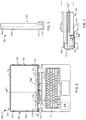
- FIG. 2 illustrates an example user device 200 including an example display device 201 constructed in accordance with teachings of this disclosure.
- the example user device 200 is a laptop, however, the user device 200 can include other user devices such as an electronic tablet (e.g., an electronic tablet that can be coupled to one or more keyboards, docketing stations, etc.).
- the example display device 201 of FIG. 2 includes a display screen 202 (e.g., an LCD panel).
- a bezel 204 is disposed around the display screen 202.
- the example bezel 204 of FIG. 2 includes a first sidewall 206 (i.e., a right sidewall relative to a user viewing the display screen 202 in the orientation illustrated in FIG.
- the sidewalls 206, 208, 210, 212 form a frame about the display screen 202.
- the bezel 204 of FIG. 2 includes side portions 209 that at least partially extend along respective right and left sides of the display device 201.
- one of the side portions 209 of the bezel is shown in FIG. 2 .
- the side portions 209 of the bezel 204 can be coupled (e.g., via mechanical or chemical fastener(s)) to a housing (e.g., a lid or a cover) that houses the display screen 202 and serves as a protective cover for the display device 201.
- the example display device 201 of FIG. 2 is coupled to a base 211 of, the user device 200 via one or more hinges 213.
- the bottom sidewall 212 of the bezel 204 includes openings to accommodate the hinge(s) 213. In other some examples, the bottom sidewall 212 of the bezel 204 does not include opening(s) for hinge(s) (e.g., when used with some electronic tablets, when used with laptops having various hinge designs, etc.). In some such examples, the bottom sidewall 212 of the bezel 204 is disposed above (i.e., entirely above) the hinges to avoid interfering with the hinge(s) of the laptop.
- one or more integrated circuits (IC(s)) 214 are coupled to (e.g., mounted on) a glass substrate 215 of the display screen 202.
- the IC(s) 214 are TCON embedded driver(s) including TCON drivers and source drivers (i.e., TED IC(s)).
- the TED IC(s) 214 are coupled to a portion 216 of the glass substrate 215 that is proximate to the bottom sidewall 212 of the bezel 204.
- the TED IC(s) 214 are coupled or bonded to the glass substrate 215 using chip-on-glass (COG) bonding.
- COG chip-on-glass
- the TED IC(s) 214 may be bonded to the glass substrate 215 using anisotropic conductive film.
- the example display device 201 of FIG. 2 includes one or more flexible printed circuits (FPC(s)) 218.
- the FPC(s) 218 include passive components such as resistors and capacitors. These passive components provide functions such as power delivery, power conditioning, facilitating communication between a motherboard 219 of the user device 200 and the TED IC(s) and/or other electrical components of the display device 201, etc.
- the FPC(s) 218 do not include the TCON chips. Rather, the TED IC(s) 214 include the TCON drivers and, thus, the example display device 201 of FIG. 2 does not include a separate TCON PCB as in the known display device 100 of FIG. 1 . Therefore, a size (e.g., a width) of the FPC(s) 218 of FIG. 2 is reduced as compared to the TCON PCB 118 of FIG. 1 .
- a width W of the bottom sidewall 212 of the bezel 204 is less than a width of the bottom sidewall 112 of the bezel 104 in the known display device 100 of FIG. 1 .
- the width of the bottom sidewall 212 of bezel 204 of FIG. 2 is reduced as compared to the bezel 104 of FIG. 1 because in the example of FIG. 2 , there are fewer electrical components to cover with the bottom sidewall 212.
- the electrical components that are to be covered by the bottom sidewall 212 e.g., the FPC(s) 218) are reduced in size (e.g., width, thickness) as compared to the electrical components of the known display device 100 of FIG.
- the width W of the bottom sidewall 212 of the bezel 204 of FIG. 2 can be approximately 5 mm.
- the width of the bottom sidewall 212 and widths of one or more of the right sidewall 206, the left sidewall 208, and/or the top sidewall 210 are the same or substantially the same.
- the widths of each of the right sidewall 206, the left sidewall 208, the top sidewall 210, and the bottom sidewall 212 are the same or substantially the same.
- the COG bonding of the TED IC(s) 214 to the display glass substrate 215 reduces a number of PCB components of the display device 201 and, thus, facilitates a reduction in a width of the bottom sidewall 212 of the bezel 204 as compared to the bezel 104 of the known display device 100 of FIG. 1 .
- an increased amount of the display screen 202 is visible to the user.
- the reduction in the width of the bottom sidewall 212 of the bezel 204 of FIG. 2 increases a screen-to-body ratio of user device 200 and provides an appearance of an edge-to-edge display screen.
- FIG. 3 is a cross-sectional view of the example display device 201 of FIG. 2 taken along the 3-3 line of FIG. 2 .
- the bezel 204 is not shown in FIG. 3 .
- the example display device 201 includes a backlight 302 disposed proximate to a backside 304 of the display screen 202, or a side of the display screen 202 that is not visible to the user.
- FIG. 3 also shows one of the TED ICs 214 of FIG. 2 coupled to the display screen 202 via COG bonding.
- the FPC(s) 218 include passive components such as resistors and capacitors, but do not include TCON chips, which are instead included in the TED IC(s) 214.
- a thickness of a side profile of the display device 201 can be defined by placement and/or size of PCB board(s), FPC(s), etc.
- the FPC(s) 218 are disposed proximate to a light guide frame ( FIG. 4 ) of the backlight 302 to reduce a thickness of the sides of the display device 201. Reducing a thickness of the sides of the display device allows a thickness of the side portion(s) 209 of the bezel 204 of FIG. 2 that at least partially extend along the sides of the display device 201 to be reduced.
- FIG. 4 is a partial, cross-sectional view of the example display device 201 of FIGS. 2 and 3 taken along the 4-4 line of FIG. 2 and showing a portion of the backlight 302 of FIG. 3 .
- the bezel 204 is not shown in FIG. 4 .
- the example backlight 302 includes a light guide frame 400 that houses at least one light source 402 (e.g., an LED).
- the light guide frame 400 can be made of, for example, aluminum.
- the backlight 302 includes a light guide pipe 404 and a plurality of optical films 406 to distribute the light emitted by the light source 402 to illuminate the display screen 202.
- the light guide frame 400 includes a cavity 408 defined therein.
- the cavity 408 can be formed in the light guide frame 400 during manufacture of the light guide frame 400 via, for example, extrusion.
- the FPC 218 of the display device 201 is positioned relative to the backlight 302 such that one or more PCB components 410 (e.g., resistors, capacitators, or electrical components) of the FPC 218 is at least partially disposed in the cavity 408.
- the PCB components 410 of the FPC 218 are stored within cavity 408 of the light guide frame of the example backlight 302 rather than consuming space elsewhere in the display device 201.
- the placement of the PCB components 410 of the FPC 218 in the cavity 408 of the light guide frame 400 maximizes use of available space in the cavity 408.
- a thickness t of the side profile of the display device 201 is reduced as compared to the known display device 100 of FIG. 1 in which the PCB components are located, for instance, behind the display screen but not within a cavity of other display device components such as the light guide frame.
- a thickness of the side portion(s) 209 of the bezel 204 required to cover components of the display device 201 such as the FPC 218 is reduced as compared to the bezel 104 of the known display device 100 of FIG. 1 .
- the side portion(s) 209 of the bezel 204 can have a thickness of 2 mm or less.
- the example display device 201 of FIG. 2 provides for a reduction in the width of the bottom sidewall 212 of the bezel 204 and a reduction in the thickness of the side portion(s) 209 of the bezel 204 that are used at least partially to cover the sides of the display device 201.
- the reduction in the width of the bottom sidewall 212 increases an area of the display screen 202 visible to the user.
- the reduction in the width of the bottom sidewall 212 and the reduction in the thickness of the side portion 209 of the bezel 204 reduces a form factor of the display device 201.
- the light source 402 of FIG. 4 is coupled to a FPC 412.
- the FPC 412 can be a different FPC than the FPC 218 that includes the passive PCB components 410.
- the FPC 412 to which the light source 402 is coupled is disposed relative to the light guide frame 400 such that the light source 402 is disposed proximate to the light guide pipe 404 to illuminate the display screen 202.
- the light source 402 is coupled to the FPC 218 in addition to the passive PCB components 410 that are coupled to the FPC 218.
- a length of the FPC 218 can be extended to relative to the example shown in FIG. 4 to enable the light source 402 to be coupled to the FPC 218 and to be disposed proximate to the light guide pipe 404.
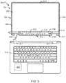
- FIG. 5 illustrates an example user device 500 including another example display device 501 in accordance with teachings of this disclosure.
- the user device 500 is a laptop, however, the example display device 501 can be used with other types of user devices (e.g., a tablet, a smartphone).
- the example display device 501 of FIG. 5 includes a display screen 502 (e.g., an LCD panel).
- a bezel 504 is disposed around the display screen 502.
- the bezel 504 of FIG. 5 is similar to the example bezel 204 of FIG. 2 .
- the bezel 504 of FIG. 5 includes a first sidewall 506 (i.e., a right sidewall relative to a user viewing the display screen 502 in the orientation illustrated in FIG.
- a second or left sidewall 508 a third or top sidewall 510, and a fourth or bottom sidewall 512.
- the sidewalls 506, 508, 510, 512 form a frame about the display screen 502.
- the bezel 504 is coupled (e.g., via mechanical or chemical fastener(s)) to a housing 511 (e.g., a lid or cover) that houses the display device 501 and serves as a protective cover for the display device 501 (e.g., when the laptop is in a folded position).
- the housing 511 includes a hinge receiving region 513.
- the display device 501 is coupled to a base 514 of the user device 500 (e.g., a portion of the user device 500 including a motherboard 509) via one or more hinges 517.
- the hinge(s) 517 are received in the hinge receiving region 513 of the housing 511 to couple the display device 501 to the base 514.
- the bottom sidewall 512 of the bezel 504 is disposed above (i.e., entirely above) the hinge(s) 517 so as not to interfere with the hinge(s) 517.
- one or more integrated circuits (IC(s)) 515 are coupled to (e.g., mounted on) an FPC 516 of the display device 501.
- the IC(s) 515 are TCON embedded drivers including TCON drivers and source drivers.
- the TED IC(s) 515 are coupled to (e.g., mounted on) the FPC 516 using chip-on-flex (COF) bonding.
- COF chip-on-flex
- COF bonding can include a die attach process in which the TED IC(s) 515 are attached to the flexible substrate of the FPC 516 and a wire bonding process to provide for electrical connections between the TED IC(s) 515 and the FPC 516.
- the FPC 516 is disposed proximate to the bottom sidewall 512 of the bezel 504.
- at least a portion of the FPC 516 is disposed in a cavity 518 formed in the hinge receiving region 513 of the housing 511 of the display device 501.
- a cable 520 is routed to extend from the cavity 518 of the hinge receiving region 513 of the housing 511 to communicatively couple the FPC 516 to the motherboard 509 of the user device 500 located at the base 514 of the user device 500.
- the amount of the FPC 516 that is to be covered by the bottom sidewall 512 of the bezel 504 is reduced as compared to if the bottom sidewall 512 was to cover all or substantially all of the FPC 516.
- the bottom sidewall 512 covers a portion of the FPC 516 that is external to or not disposed in the cavity 518 of the hinge receiving region 513 of the housing 511.
- the bottom sidewall 512 covers at least a portion of the TED IC(s) 515.
- the TED IC(s) 515 are disposed in the cavity 518 and such that the bottom sidewall 512 covers a portion the FPC 516 that does not include the TED IC(s) 515.
- a width W of the bottom sidewall 512 of FIG. 5 is reduced as compared to the width of the bottom sidewall 112 of the bezel 104 of the known display device 100 of FIG. 1 .
- the width W of the bottom sidewall 512 of FIG. 5 is approximately 3 mm.
- the example display device 501 of FIG. 5 provides for an increased a screen-to-body ratio of the user device 500.
- the width of the bottom sidewall 512 and widths of one or more of the right sidewall 506, the left sidewall 508, and/or the top sidewall 510 are the same or substantially the same. In some examples, the widths of each of the right sidewall 506, the left sidewall 508, the top sidewall 510, and the bottom sidewall 512 are the same or substantially the same.
- the example display devices 201, 501 of FIGS. 2-5 include bezels having bottom sidewalls with substantially reduced widths as compared to known bezels (e.g., the bezel 104 of FIG. 1 ).
- the number of PCB components of the display devices 201, 501 is reduced, which provides for increased flexibility in adjusting the position of the FPCs and, accordingly, enables a reduction in the width of the bottom sidewalls 212, 512 of the bezels 204, 504.
- components of the user device such as the hinge receiving region 513 of the laptop housing or lid 511 receive a portion of the FPC.
- the bottom sidewall 512 of the bezel 504 covers less of the FPC and, thus, a width of the bottom sidewall 512 can be reduced.
- the example display devices 201, 501 facilitate the appearance of an edge-to-edge display screen or a substantially bezel-less display screen.
- components of the display device such as the light guide frame 400, are used to store FPC components, thereby enabling a thickness of the side profile of the display device to be reduced and decreasing a form factor of the user device.
- a backlight of the display device can facilitate reductions in a thickness of the side portions of the bezel (e.g., the side portion(s) 209 of FIG. 2 ) that at least partially cover the sides of the display device.
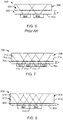
- FIG. 6 illustrates a known backlight 600 of a display device. As shown in FIG. 6 , a gap 602 is defined between a light guide panel 603, which includes LED light sources 604 coupled thereto, and a display screen 606 of the display device.
- the gap 602 provides an area for light emitted by the respective LED light sources 604 to integrate and form a uniform or substantially uninform light that illuminates the display screen 606, defining an active area 608 or a viewable area of the display screen 606.
- the gap 602 enables the light emitted by the respective LED light sources 604 to integrate to reduce instance of hot spots or irregularities in the light distribution that may cause portions of the display screen 606 to appear brighter than other portions.
- a width of the gap between the light guide panel and the display screen is reduced as compared to the width w of the gap 602 of the known backlight of FIG. 6 .
- a decrease in the size of the gap reduces a thickness of the display profile and thus, allows a thickness of the side portions of the bezel to be reduced as compared to display device including larger gaps between the light guide panel and the display screen.
- the smaller gap size allows the light sources to be located closer to the display screen.
- an amount or density of the light that illuminates the edges of the display screen is increased, thereby increasing an active area of the LCD display screen and allowing more of the display screen to be viewed by a user.
- the increased viewable or active area of the display screen further provides for the appearance of an edge-to-edge display screen when used with the, for instance, the example bezels 204, 504 of FIGS. 2-5 .
- FIG. 7 illustrates an example backlight 700 for use with a display device (e.g., the example display devices 201, 501 of FIGS. 2-5 ) in accordance with teachings of this disclosure.
- the backlight 700 of FIG. 7 includes a plurality of lights sources 702 coupled to a light guide panel 704.
- the light sources 702 can include one-chip LEDs.
- the example backlight 700 can include additional or fewer light sources 702 than illustrated in FIG. 7 .
- a gap 706 is defined between the light guide panel 704 and a display screen 708 (e.g., an LCD panel) of the display device.
- spacers 710 e.g., photo spacers made of, for instance, silicon dioxide
- the example spacers 710 include reflective coatings (e.g., white paint) to help diffuse the light and improve uniformity of the light emitted by the respective light sources 702. Therefore, a distance of the gap 706 over which the light emitted by the respective light sources 702 travels before integrating and forming a substantially uniform light is reduced as compared to backlights that do not include the spacers 710 to facilitate distribution of the light emitted by each of the light sources 702.
- a width w of the gap 706 can be decreased as compared to the width of the gap 602 in the known backlight 600 of FIG. 6 .
- the light sources 702 are located closer to the display screen 708.
- an area of the display screen 708 that is illuminated by the backlight 700 i.e., an active area 712, is increased.
- the example lights sources 702 of FIG. 7 increase an amount or a density of the light that illuminates the edges 714 of the display screen 708 due to the increased proximity of the light sources 702 to the display screen 708.
- distribution of the light at the edges 714 of the display screen 708 is increased in the example of FIG.
- the expanded active area 712 of the display screen 708 improves viewing of the display screen 708 in examples in which the bezel of a user device (e.g., the bezels 204, 504 of FIGS. 2-5 ) includes narrow sidewalls and, thus, the viewable area of the display screen is increased, as in edge-to-edge display screens.
- the bezel of a user device e.g., the bezels 204, 504 of FIGS. 2-5
- the viewable area of the display screen is increased, as in edge-to-edge display screens.
- FIG. 8 illustrates an example backlight 800 including a one or more two-chip (or n chip) LED lights sources 802 and a light guide panel 804.
- the example backlight 800 can include additional or fewer light sources 802 than illustrated in FIG. 8 .
- a gap 806 is defined between the light guide panel 804 and a display screen 808 (e.g., LCD panel) of the display device.
- a spacer 810 e.g., a photo spacer
- a reflective coating e.g., white paint
- a width w of the gap 806 of the example backlight 800 of FIG. 8 is reduced as compared to backlights that do not include the spacer 810 to diffuse the light emitted by the light(s) of the backlight.
- the use of the two-chip (or n chip) LED light source(s) 802 increases an amount of a density of the light that illuminates the edges 814 of the display screen 808.
- a viewable or active area 812 of the display screen 808 is increased as compared to the active area 608 of the display screen 606 in FIG 6 .
- the example backlights 700, 800 of FIGS. 7 and/or 8 are not limited to backlights including the light sources 702, 802 and/or spacers 710, 810 of FIGS. 7 and 8 .
- Other arrangements of the light sources, such as a string of mini LED lights can be used to improve light distribution and reduce a width of the gap between the light sources and the display screen and, thus, reduce a width of the display device profile.
- FIG. 9 is a flowchart of an example method 900 for manufacturing a display device such as the example display device 201 of FIGS. 2-4 .
- the IC(s) 214 e.g., TCON embedded (TED) IC(s)
- the TED IC(s) 214 are bonded to the glass substrate 215 using chip-on-glass bonding.
- passive PCB components 410 such as resistors and capacitors are coupled to the flexible printed circuit (FPC) 218.
- the FPC 218 and the passive PCB components 410 facilitate communication between the TED IC(s) 214 and a motherboard 219 of a user device including the example display device 201 (e.g., the user device 200 of FIG. 2 ).
- a cavity 408 is in formed in the light guide frame 400 of the backlight 302 of the example display device 201 of FIGS. 2-4 .
- the cavity 408 of the light guide frame 400 is formed prior to the coupling of, for example, the light source 402 to the light guide frame 400.
- the cavity 408 can be formed in the light guide frame 400 via, for example, an extrusion process during manufacturing of the light guide frame 400.
- the FPC 218 is positioned relative to the backlight 302 such that the passive PCB components 410 of the FPC 218 are at least partially disposed in the cavity 408 of the light guide frame 400, thereby reducing a thickness of a profile (e.g., a side profile) and/or a form factor of the example display device 201 when assembled.
- a profile e.g., a side profile
- the bezel 204 is disposed about the display screen 202 to frame the display screen 202 (e.g., by coupling the bezel 204 to a lid or cover of the user device 200).
- a bottom sidewall 212 of the bezel 204 has a reduced width as compared to bezels of known display devices, thereby increasing a viewable area of the display screen 202 and a screen-to-body ratio of the user device including the display device 201.
- FIG. 10 is a flowchart of an example method 1000 for manufacturing a display device such as the example display device 501 of FIG. 5 .
- the IC(s) 515 e.g., TCON embedded (TED) IC(s)
- FPC flexible printed circuit
- the TED IC(s) 515 are bonded to the FPC 516 using chip-on-flex bonding.
- At block 1004 at least a portion of the FPC 516 is disposed in a cavity 518 of the hinge receiving region 513 of a housing 511 (e.g., lid or cover) of the display device 501 of FIG. 5 .
- a cable 520 is routed through the hinge receiving region 513 of the housing 511 to communicatively couple the FPC 516 to a motherboard 509 located in at the base 514 of the user device 500.
- the bezel 504 is disposed about the display screen 502 to frame the display screen 502 (e.g., by coupling the bezel 504 to the housing 511 of the user device 500).
- a bottom sidewall 512 of the bezel 504 has a reduced width as compared to bezels of known display devices, thereby increasing a viewable area of the display screen 502 and a screen-to-body ratio of the user device 500 including the display device 501.
- example methods 900, 1000 are described with reference to the flowcharts illustrated in FIGS. 9 and 10 , many other methods of manufacturing the example display device 201 of FIGS. 2-4 and/or the example display device 501 of FIG. 5 may alternatively be used.
- the order of execution of the blocks may be changed, and/or some of the blocks described may be changed, eliminated, or combined.
- additional operations may be included in the manufacturing process before, in between, or after the blocks shown in FIGS. 9 and/or 10.
- example apparatus, articles of manufacture, and methods have been disclosed herein to reduce a width of a bezel or frame surrounding a display screen of an electronic user device and, as a result, increase a screen-to-body ratio of the user device.
- bonding techniques such as COG and COF bonding are used to mount TED IC(s) on substrates such as a glass substrate of a display screen (e.g., LCD panel) or a flexible printed circuit.
- Examples disclosed herein reduce a number of PCB components of the display device, which enables a width of a sidewall or border of the bezel (e.g., a bottom border of the bezel) covering the electrical components of the display device to be reduced.
- an edge-to-edge display is substantially achieved relative to each of the borders of the bezel.
- A, B, and/or C refers to any combination or subset of A, B, C such as (1) A alone, (2) B alone, (3) C alone, (4) A with B, (5) A with C, (6) B with C, and (7) A with B and with C.
- the phrase "at least one of A and B" is intended to refer to implementations including any of (1) at least one A, (2) at least one B, and (3) at least one A and at least one B.
- the phrase "at least one of A or B" is intended to refer to implementations including any of (1) at least one A, (2) at least one B, and (3) at least one A and at least one B.
- the phrase "at least one of A and B" is intended to refer to implementations including any of (1) at least one A, (2) at least one B, and (3) at least one A and at least one B.
- the phrase "at least one of A or B" is intended to refer to implementations including any of (1) at least one A, (2) at least one B, and (3) at least one A and at least one B.
Landscapes
- Physics & Mathematics (AREA)
- Engineering & Computer Science (AREA)
- General Physics & Mathematics (AREA)
- Theoretical Computer Science (AREA)
- Computer Hardware Design (AREA)
- Optics & Photonics (AREA)
- Nonlinear Science (AREA)
- General Engineering & Computer Science (AREA)
- Human Computer Interaction (AREA)
- Mathematical Physics (AREA)
- Chemical & Material Sciences (AREA)
- Crystallography & Structural Chemistry (AREA)
- Microelectronics & Electronic Packaging (AREA)
- Computer Networks & Wireless Communication (AREA)
- Devices For Indicating Variable Information By Combining Individual Elements (AREA)
- Liquid Crystal (AREA)
Abstract
Description
- This disclosure relates generally to display devices and, more particularly, to edge-to-edge display devices and related methods.
- An electronic user device such as a laptop, or tablet, or other personal computing (PC) device includes a display screen to enable a user to interact with content displayed on the screen via graphical user interfaces. The user device includes a bezel or a frame disposed around the edges of the display screen. Along with housing (e.g., a cover or lid) of the user device that houses the display screen, the bezel structurally supports the display screen when, for example, the display screen is coupled to another component such as base of a laptop including a keyboard. The bezel also protects electrical components associated with and disposed proximate to the display screen, such as printed circuit boards, source drivers, etc., from external exposure.
- Screen-to-body ratio represents an amount of display screen surface relative to an amount of body surface of the electronic device. A electronic device having a high screen-to-body ratio typically includes a bezel that forms a narrow border around the display screen of the device and, thus, defines a larger display screen area that is visible to the user, as compared to a device with a smaller screen-to-body ratio.
-
-
FIG. 1 is a schematic illustration of a known display device. -
FIG. 2 is a schematic illustration of an example display device constructed in accordance with teachings of this disclosure. -
FIG. 3 is a cross-sectional view of the example display device ofFIG. 2 taken along the 3-3 line ofFIG. 2 . -
FIG. 4 is a partial cross-sectional view of the example display device ofFIGS. 2 and 3 taken along the 4-4 line ofFIG. 2 . -
FIG. 5 is a schematic illustration of another example display device constructed in accordance with teachings of this disclosure. -
FIG. 6 is a schematic illustration of a known backlight of a display device. -
FIG. 7 is a schematic illustration of an example backlight of a display device constructed in accordance with teachings of this disclosure. -
FIG. 8 is a schematic illustration of another example backlight of a display device constructed in accordance with teachings of this disclosure. -
FIG. 9 is a flowchart of an example method to manufacture the example display device ofFIGS. 2-4 . -
FIG. 10 is a flowchart of an example method to manufacture the example display device ofFIG. 5 . - The figures are not to scale. Instead, the thickness of the layers or regions may be enlarged in the drawings. In general, the same reference numbers will be used throughout the drawing(s) and accompanying written description to refer to the same or like parts.
- A display screen of an electronic user device such as a laptop, tablet, or other personal computing (PC) device enables a user to interact with content such as user applications installed on the user device, media accessed via the Internet, etc., via graphical user interfaces that are presented on the display screen. The display screen (e.g., an LCD panel) is typically surrounded by a frame, border, or bezel that defines a perimeter of the display screen. The bezel can be coupled to a housing (e.g., a cover or lid) of the user device that houses the display screen and other electronic components of a display device that includes the display screen. The bezel structurally supports the display screen by framing or holding the display screen when the display screen is, for example, used with a laptop. In some examples, the bezel covers one or more electrical components associated with the display device, such as source drivers, backlight drivers, and timing controller (TCON) chip(s) disposed on a printed circuit board (PCB) proximate to the display screen. In such examples, the bezel protects the electrical components of the display device from external exposure, prevents debris from damaging the electrical components, etc.
- A bezel includes sidewalls that extend along a right side of the display screen (e.g., relative to a user viewing the display the screen), a left side of the display screen, a top of the display screen, and a bottom of the display screen. Screen-to-body ratio represents an amount of display screen surface relative to an amount of body surface of the PC device. Increasing the screen-to-body ratio can be achieved by reducing a width of one or more sidewalls of the bezel surrounding the display screen, thereby increasing an amount of the display screen that is visible to the user. For example, the widths of the top, right, and left sidewalls of the bezel may be reduced so as to give the user the appearance that the display screen extends from edge-to-edge, or put another way, is substantially bezel-less or borderless.
- As mentioned above, at least a portion of the bezel, such as the bottom sidewall, may cover electrical components of the display screen, such as source driver integrated circuit(s) (IC(s)) that may be bonded to a glass substrate of the display panel and the TCON PCB. The TCON PCB may be disposed proximate to the bottom sidewall of the bezel to facilitate efficient communicative coupling with, for example, a motherboard of a laptop that may be located at a base of the laptop, or the portion including the keyboard. A bezel having a narrow bottom sidewall may not adequately cover the electrical components of the display screen. Thus, some known bezels include narrow top, right, and left sidewalls but have wider bottom sidewalls to cover the electrical components. The wider bottom sidewall limits the screen-to-body ratio that can be achieved using such bezels.
- In some known user devices, the TCON PCB is disposed on the motherboard of the electronic device, which can be housed in a portion of the user device that is separate from the display screen, such as a base of a laptop). Moving the TCON PCB away from the portion of the device including the display screen may permit use of a bezel including a narrower bottom sidewall to be used to frame the display screen. However, moving the TCON PCB introduces complications with respect to routing signals between the TCON PCB and the source driver IC(s). For example, cables that communicatively couple the TCON PCB to the display screen and/or the source driver IC(s) may need to be routed through hinge(s) of the user device that secure the portion of the device including the TCON PCB to the portion of the device including the display screen. Such a routing of cables can affect signal integrity and introduce electromagnetic interference concerns.
- Some other known attempts to increase the screen-to-body ratio and an edge-to-edge appearance of the display screen include adjusting a size of the TCON PCB and/or moving the TCON PCB behind the display screen within the housing of the display device. A size and/or configuration of the TCON PCB may be adjusted by using a flexible PCB to, for example, fit the TCON PCB behind the display screen or reduce a width of the TCON PCB when the TCON PCB is disposed near the bottom sidewall of the bezel. However, although the size and/or configuration of the flexible TCON PCB may be adjusted, the number of components coupled to the TCON PCB has not changed. Thus, a thickness of the TCON PCB may be increased to accommodate the active components (e.g., TCON chip(s)) and the passive components (e.g., resistors, capacitators) coupled to the PCB. An increase in the thickness of the PCB may increase a thickness of a profile of the display device (e.g., a side profile of the display device) and, thus, impact the form factor of the user device.
- Disclosed herein are example bezels to be disposed about a display screen of a display device that include narrow sidewalls to increase the screen-to-body ratio of a user device that includes the display device. In some examples disclosed herein, an integrated circuit (IC) including a timing controller and a source driver (i.e., TCON embedded driver (TED) IC) is coupled to (e.g., mounted) on a glass substrate of the display screen using chip-on-glass (COG) bonding. The use of the TED IC reduces a number of PCB components of the display device as compared to display devices that include a TCON PCB. In some examples, the flexible printed circuits (FPCs) including passive components (e.g., resistors, capacitors) can be disposed within the display device without increasing the thickness of a side profile of the display device. Thus, in examples disclosed herein, a bezel having a narrow bottom sidewall can be used to increase the visible display screen area without negatively impacting the form factor of the user device and/or the operation of the device.
- In some other examples disclosed herein, an IC (e.g., a TED IC) is coupled to (e.g., mounted on) an FPC via chip-on-flex bonding. In such examples, at least a portion of the FPC is disposed in a portion of a lid or cover of a user device such as a laptop that receives hinge(s) to couple the display screen to a base of the user device (e.g., a portion of a laptop including a motherboard, a keyboard, etc.). As a result, an amount of the FPC to be covered by the bottom sidewall of the bezel is reduced as compared to known display devices including TCON PCBs that are located in the hinge region of the device. Thus, a width of the bottom sidewall of the example bezels disclosed herein can be reduced and the screen-to-body ratio of the user device can be increased.
- Also disclosed herein are example backlights that improve uniform distribution of light emitted by a plurality of light sources (e.g., light-emitting diodes) to illuminate a display screen of a display device. The light sources of the backlight are spaced apart from the display screen by a gap over which light emitted by the respective light sources travels and integrates to form a substantially uniform light to illuminate the display screen. In some examples disclosed herein, spacers (e.g., photo spacers) are disposed between the respective light sources. Example spacers disclosed herein include a reflective coating to facilitate the distribution of light emitted by the light sources. In examples disclosed herein, the size of the gap between the light sources and the display screen can be reduced as compared to known backlights because of the improved distribution light due to the spacers located at the light sources. In reducing the gap between the light sources and the display screen, a thickness of a side profile of the display device can be reduced. As a result, a thickness of a portion of the bezel that covers or partially covers the sides of the display device can be reduced.
- Although examples disclosed herein are primarily discussed in the context of user devices such as laptops, the example displays disclosed herein can be utilized with other electronic display devices, such as televisions, smartphones, desktop monitors, tablets, etc. As such, the discussion of display devices for laptops is for illustrative purposes only and does not limit this disclosure to use with laptops.
-
FIG. 1 illustrates adisplay device 100 known in the prior art. The knowndisplay device 100 can be used with an electronic user device such as a laptop or a tablet. The knowndisplay device 100 includes a display screen 102 (e.g., an LCD panel). Abezel 104 is disposed around thedisplay screen 102. Thebezel 104 includes a first sidewall 106 (i.e., a right sidewall relative to a user viewing thedisplay screen 102 in the orientation illustrated inFIG. 1 ), a second or leftsidewall 108, a third ortop sidewall 110, and a fourth orbottom sidewall 112. - The
display screen 102 includes a plurality ofsource drivers 114 coupled to (e.g., mounted on) aglass substrate 115 of thedisplay screen 102 via, for instance, chip-on-glass bonding. As shown inFIG. 1 , thesource drivers 114 are disposed proximate to aportion 116 of thedisplay screen 102 covered by thebottom sidewall 112 of thebezel 104. Thedisplay device 100 includes a timing controller (TCON)PCB board 118. TheTCON PCB board 118 is communicatively coupled to thesource drivers 114 via one or more flexible printed circuits (FPC(s)) 120. TheTCON PCB board 118 is communicatively coupled to a motherboard of the user device that includes thedisplay device 100, such as a laptop, via cables that extend from the display device to a base of the laptop. - As shown in
FIG. 1 , thesidewalls bezel 104 cover theportion 116 of the display screen including thesource drivers 114 and the right, left, and top edges of thedisplay screen 102. As also shown inFIG. 1 , thebottom sidewall 112 has a width W1 that is greater than a width W2 of any of the right, left, andtop sidewalls bottom sidewall 112 covers a greater portion of thedisplay screen 102 than theother sidewalls bottom sidewall 112 is increased relative to the widths of theother sidewalls source drivers 114, the FPC(s) 120, theTCON PCB 118, etc. InFIG. 1 , the width W1 of thebottom sidewall 112 ranges from 7 mm to 18 mm. - The
bezel 104 ofFIG. 1 includesside portions 122, or portions that extend at least partially along the respective right and left sides of thedisplay device 100 and that can couple to a housing (e.g., a backing or cover) of thedisplay device 100. One of theside portions 122 is shown inFIG. 1 . InFIG. 1 , a thickness t of aside portion 122 of thebezel 104 is about 4.5 mm. The side portion(s) 122 of thebezel 104 at least partially cover theTCON PCB 118. The side portion(s) 122 of thebezel 104 may also cover or partially electrical components of the knowndisplay device 100 disposed behind thedisplay screen 102, such as a backlight (e.g., including LED light sources, light pipes, optical films). -
FIG. 2 illustrates an example user device 200 including anexample display device 201 constructed in accordance with teachings of this disclosure. The example user device 200 is a laptop, however, the user device 200 can include other user devices such as an electronic tablet (e.g., an electronic tablet that can be coupled to one or more keyboards, docketing stations, etc.). Theexample display device 201 ofFIG. 2 includes a display screen 202 (e.g., an LCD panel). Abezel 204 is disposed around thedisplay screen 202. Theexample bezel 204 ofFIG. 2 includes a first sidewall 206 (i.e., a right sidewall relative to a user viewing thedisplay screen 202 in the orientation illustrated inFIG. 2 ), a second or leftsidewall 208, a third ortop sidewall 210, and a fourth orbottom sidewall 212. As shown inFIG. 2 , thesidewalls display screen 202. - The
bezel 204 ofFIG. 2 includesside portions 209 that at least partially extend along respective right and left sides of thedisplay device 201. For illustrative purposes, one of theside portions 209 of the bezel is shown inFIG. 2 . In the exampleFIG. 2 , theside portions 209 of thebezel 204 can be coupled (e.g., via mechanical or chemical fastener(s)) to a housing (e.g., a lid or a cover) that houses thedisplay screen 202 and serves as a protective cover for thedisplay device 201. Theexample display device 201 ofFIG. 2 is coupled to abase 211 of, the user device 200 via one or more hinges 213. In some examples, thebottom sidewall 212 of thebezel 204 includes openings to accommodate the hinge(s) 213. In other some examples, thebottom sidewall 212 of thebezel 204 does not include opening(s) for hinge(s) (e.g., when used with some electronic tablets, when used with laptops having various hinge designs, etc.). In some such examples, thebottom sidewall 212 of thebezel 204 is disposed above (i.e., entirely above) the hinges to avoid interfering with the hinge(s) of the laptop. - In the example of
FIG. 2 , one or more integrated circuits (IC(s)) 214 are coupled to (e.g., mounted on) aglass substrate 215 of thedisplay screen 202. In the example ofFIG. 2 , the IC(s) 214 are TCON embedded driver(s) including TCON drivers and source drivers (i.e., TED IC(s)). As shown in the example ofFIG. 2 , the TED IC(s) 214 are coupled to aportion 216 of theglass substrate 215 that is proximate to thebottom sidewall 212 of thebezel 204. In the example ofFIG. 2 , the TED IC(s) 214 are coupled or bonded to theglass substrate 215 using chip-on-glass (COG) bonding. For example, the TED IC(s) 214 may be bonded to theglass substrate 215 using anisotropic conductive film. - The
example display device 201 ofFIG. 2 includes one or more flexible printed circuits (FPC(s)) 218. In the example ofFIG. 2 , the FPC(s) 218 include passive components such as resistors and capacitors. These passive components provide functions such as power delivery, power conditioning, facilitating communication between amotherboard 219 of the user device 200 and the TED IC(s) and/or other electrical components of thedisplay device 201, etc. - As compared to the known
display device 100 ofFIG. 1 including theTCON PCB 118, in the example ofFIG. 2 , the FPC(s) 218 do not include the TCON chips. Rather, the TED IC(s) 214 include the TCON drivers and, thus, theexample display device 201 ofFIG. 2 does not include a separate TCON PCB as in the knowndisplay device 100 ofFIG. 1 . Therefore, a size (e.g., a width) of the FPC(s) 218 ofFIG. 2 is reduced as compared to theTCON PCB 118 ofFIG. 1 . As a result, a width W of thebottom sidewall 212 of thebezel 204 is less than a width of thebottom sidewall 112 of thebezel 104 in the knowndisplay device 100 ofFIG. 1 . In particular, the width of thebottom sidewall 212 ofbezel 204 ofFIG. 2 is reduced as compared to thebezel 104 ofFIG. 1 because in the example ofFIG. 2 , there are fewer electrical components to cover with thebottom sidewall 212. Additionally or alternatively, the electrical components that are to be covered by the bottom sidewall 212 (e.g., the FPC(s) 218) are reduced in size (e.g., width, thickness) as compared to the electrical components of the knowndisplay device 100 ofFIG. 1 (e.g., the TCON PCB 118). For example, the width W of thebottom sidewall 212 of thebezel 204 ofFIG. 2 can be approximately 5 mm. In some examples, the width of thebottom sidewall 212 and widths of one or more of theright sidewall 206, theleft sidewall 208, and/or thetop sidewall 210 are the same or substantially the same. In some examples, the widths of each of theright sidewall 206, theleft sidewall 208, thetop sidewall 210, and thebottom sidewall 212 are the same or substantially the same. - In the example of
FIG. 2 , the COG bonding of the TED IC(s) 214 to thedisplay glass substrate 215 reduces a number of PCB components of thedisplay device 201 and, thus, facilitates a reduction in a width of thebottom sidewall 212 of thebezel 204 as compared to thebezel 104 of the knowndisplay device 100 ofFIG. 1 . As result, an increased amount of thedisplay screen 202 is visible to the user. The reduction in the width of thebottom sidewall 212 of thebezel 204 ofFIG. 2 increases a screen-to-body ratio of user device 200 and provides an appearance of an edge-to-edge display screen. -
FIG. 3 is a cross-sectional view of theexample display device 201 ofFIG. 2 taken along the 3-3 line ofFIG. 2 . For illustrative purposes, thebezel 204 is not shown inFIG. 3 . As illustrated inFIG. 3 , theexample display device 201 includes abacklight 302 disposed proximate to abackside 304 of thedisplay screen 202, or a side of thedisplay screen 202 that is not visible to the user.FIG. 3 also shows one of theTED ICs 214 ofFIG. 2 coupled to thedisplay screen 202 via COG bonding. - As discussed above, in the example of
FIG. 2 , the FPC(s) 218 include passive components such as resistors and capacitors, but do not include TCON chips, which are instead included in the TED IC(s) 214. A thickness of a side profile of thedisplay device 201 can be defined by placement and/or size of PCB board(s), FPC(s), etc. As disclosed herein, in the example ofFIGS. 2 and 3 , the FPC(s) 218 are disposed proximate to a light guide frame (FIG. 4 ) of thebacklight 302 to reduce a thickness of the sides of thedisplay device 201. Reducing a thickness of the sides of the display device allows a thickness of the side portion(s) 209 of thebezel 204 ofFIG. 2 that at least partially extend along the sides of thedisplay device 201 to be reduced. -
FIG. 4 is a partial, cross-sectional view of theexample display device 201 ofFIGS. 2 and 3 taken along the 4-4 line ofFIG. 2 and showing a portion of thebacklight 302 ofFIG. 3 . For illustrative purposes, thebezel 204 is not shown inFIG. 4 . Theexample backlight 302 includes alight guide frame 400 that houses at least one light source 402 (e.g., an LED). Thelight guide frame 400 can be made of, for example, aluminum. Thebacklight 302 includes alight guide pipe 404 and a plurality ofoptical films 406 to distribute the light emitted by thelight source 402 to illuminate thedisplay screen 202. - In the example of
FIG. 4 , thelight guide frame 400 includes acavity 408 defined therein. Thecavity 408 can be formed in thelight guide frame 400 during manufacture of thelight guide frame 400 via, for example, extrusion. As illustrated inFIG. 4 , theFPC 218 of thedisplay device 201 is positioned relative to thebacklight 302 such that one or more PCB components 410 (e.g., resistors, capacitators, or electrical components) of theFPC 218 is at least partially disposed in thecavity 408. Thus, thePCB components 410 of theFPC 218 are stored withincavity 408 of the light guide frame of theexample backlight 302 rather than consuming space elsewhere in thedisplay device 201. The placement of thePCB components 410 of theFPC 218 in thecavity 408 of thelight guide frame 400 maximizes use of available space in thecavity 408. As a result of the storage of thePCB components 410 within thecavity 408, a thickness t of the side profile of thedisplay device 201 is reduced as compared to the knowndisplay device 100 ofFIG. 1 in which the PCB components are located, for instance, behind the display screen but not within a cavity of other display device components such as the light guide frame. Accordingly, a thickness of the side portion(s) 209 of thebezel 204 required to cover components of thedisplay device 201 such as theFPC 218 is reduced as compared to thebezel 104 of the knowndisplay device 100 ofFIG. 1 . For example, the side portion(s) 209 of thebezel 204 can have a thickness of 2 mm or less. Thus, theexample display device 201 ofFIG. 2 provides for a reduction in the width of thebottom sidewall 212 of thebezel 204 and a reduction in the thickness of the side portion(s) 209 of thebezel 204 that are used at least partially to cover the sides of thedisplay device 201. The reduction in the width of thebottom sidewall 212 increases an area of thedisplay screen 202 visible to the user. Further, the reduction in the width of thebottom sidewall 212 and the reduction in the thickness of theside portion 209 of thebezel 204 reduces a form factor of thedisplay device 201. - In some examples, the
light source 402 ofFIG. 4 is coupled to aFPC 412. As shown inFIG. 4 , theFPC 412 can be a different FPC than theFPC 218 that includes thepassive PCB components 410. In the example ofFIG. 4 , theFPC 412 to which thelight source 402 is coupled is disposed relative to thelight guide frame 400 such that thelight source 402 is disposed proximate to thelight guide pipe 404 to illuminate thedisplay screen 202. In other examples, thelight source 402 is coupled to theFPC 218 in addition to thepassive PCB components 410 that are coupled to theFPC 218. In such examples, a length of theFPC 218 can be extended to relative to the example shown inFIG. 4 to enable thelight source 402 to be coupled to theFPC 218 and to be disposed proximate to thelight guide pipe 404. -
FIG. 5 illustrates anexample user device 500 including anotherexample display device 501 in accordance with teachings of this disclosure. In the example ofFIG. 5 , theuser device 500 is a laptop, however, theexample display device 501 can be used with other types of user devices (e.g., a tablet, a smartphone). Theexample display device 501 ofFIG. 5 includes a display screen 502 (e.g., an LCD panel). Abezel 504 is disposed around thedisplay screen 502. Thebezel 504 ofFIG. 5 is similar to theexample bezel 204 ofFIG. 2 . For instance, thebezel 504 ofFIG. 5 includes a first sidewall 506 (i.e., a right sidewall relative to a user viewing thedisplay screen 502 in the orientation illustrated inFIG. 5 ), a second or leftsidewall 508, a third ortop sidewall 510, and a fourth orbottom sidewall 512. As shown inFIG. 5 , thesidewalls display screen 502. - In the example of
FIG. 5 , thebezel 504 is coupled (e.g., via mechanical or chemical fastener(s)) to a housing 511 (e.g., a lid or cover) that houses thedisplay device 501 and serves as a protective cover for the display device 501 (e.g., when the laptop is in a folded position). Thehousing 511 includes ahinge receiving region 513. InFIG. 5 , thedisplay device 501 is coupled to abase 514 of the user device 500 (e.g., a portion of theuser device 500 including a motherboard 509) via one or more hinges 517. At least a portion of the hinge(s) 517 are received in thehinge receiving region 513 of thehousing 511 to couple thedisplay device 501 to thebase 514. In the example ofFIG. 5 , thebottom sidewall 512 of thebezel 504 is disposed above (i.e., entirely above) the hinge(s) 517 so as not to interfere with the hinge(s) 517. - In the example of
FIG. 5 , one or more integrated circuits (IC(s)) 515 are coupled to (e.g., mounted on) anFPC 516 of thedisplay device 501. In the example ofFIG. 5 , the IC(s) 515 are TCON embedded drivers including TCON drivers and source drivers. In the example ofFIG. 5 , the TED IC(s) 515 are coupled to (e.g., mounted on) theFPC 516 using chip-on-flex (COF) bonding. For example, COF bonding can include a die attach process in which the TED IC(s) 515 are attached to the flexible substrate of theFPC 516 and a wire bonding process to provide for electrical connections between the TED IC(s) 515 and theFPC 516. - As illustrated in
FIG. 5 , theFPC 516 is disposed proximate to thebottom sidewall 512 of thebezel 504. In the example ofFIG. 5 , at least a portion of theFPC 516 is disposed in acavity 518 formed in thehinge receiving region 513 of thehousing 511 of thedisplay device 501. InFIG. 5 , acable 520 is routed to extend from thecavity 518 of thehinge receiving region 513 of thehousing 511 to communicatively couple theFPC 516 to themotherboard 509 of theuser device 500 located at thebase 514 of theuser device 500. - As a result of the disposal of a portion of the
FPC 516 in thehinge receiving region 513 of thehousing 511, the amount of theFPC 516 that is to be covered by thebottom sidewall 512 of thebezel 504 is reduced as compared to if thebottom sidewall 512 was to cover all or substantially all of theFPC 516. For example, thebottom sidewall 512 covers a portion of theFPC 516 that is external to or not disposed in thecavity 518 of thehinge receiving region 513 of thehousing 511. In some examples, thebottom sidewall 512 covers at least a portion of the TED IC(s) 515. In other examples, the TED IC(s) 515 are disposed in thecavity 518 and such that thebottom sidewall 512 covers a portion theFPC 516 that does not include the TED IC(s) 515. Thus, a width W of thebottom sidewall 512 ofFIG. 5 is reduced as compared to the width of thebottom sidewall 112 of thebezel 104 of the knowndisplay device 100 ofFIG. 1 . In some examples, the width W of thebottom sidewall 512 ofFIG. 5 is approximately 3 mm. Thus, theexample display device 501 ofFIG. 5 provides for an increased a screen-to-body ratio of theuser device 500. In some examples, the width of thebottom sidewall 512 and widths of one or more of theright sidewall 506, theleft sidewall 508, and/or thetop sidewall 510 are the same or substantially the same. In some examples, the widths of each of theright sidewall 506, theleft sidewall 508, thetop sidewall 510, and thebottom sidewall 512 are the same or substantially the same. - Thus, the
example display devices FIGS. 2-5 include bezels having bottom sidewalls with substantially reduced widths as compared to known bezels (e.g., thebezel 104 ofFIG. 1 ). As a result of the use of TED IC(s) 214, 515 and bonding processes such as COG and COF, the number of PCB components of thedisplay devices bottom sidewalls bezels example display device 501 ofFIG. 5 , components of the user device such as thehinge receiving region 513 of the laptop housing orlid 511 receive a portion of the FPC. As a result, thebottom sidewall 512 of thebezel 504 covers less of the FPC and, thus, a width of thebottom sidewall 512 can be reduced. Accordingly, theexample display devices display device 201 ofFIGS. 2-4 , components of the display device, such as thelight guide frame 400, are used to store FPC components, thereby enabling a thickness of the side profile of the display device to be reduced and decreasing a form factor of the user device. - In some examples, in addition to or as an alternative to the PCB component(s) discussed in connection with
FIGS. 2-5 that enable a width of the bottom sidewall of the bezel to be reduced (e.g., the use of TED ICs, the positioning of the FPCs), a backlight of the display device can facilitate reductions in a thickness of the side portions of the bezel (e.g., the side portion(s) 209 ofFIG. 2 ) that at least partially cover the sides of the display device.FIG. 6 illustrates a knownbacklight 600 of a display device. As shown inFIG. 6 , agap 602 is defined between a light guide panel 603, which includes LEDlight sources 604 coupled thereto, and adisplay screen 606 of the display device. Thegap 602 provides an area for light emitted by the respective LEDlight sources 604 to integrate and form a uniform or substantially uninform light that illuminates thedisplay screen 606, defining anactive area 608 or a viewable area of thedisplay screen 606. Thegap 602 enables the light emitted by the respective LEDlight sources 604 to integrate to reduce instance of hot spots or irregularities in the light distribution that may cause portions of thedisplay screen 606 to appear brighter than other portions. - In example backlights disclosed herein, a width of the gap between the light guide panel and the display screen is reduced as compared to the width w of the
gap 602 of the known backlight ofFIG. 6 . As disclosed herein, a decrease in the size of the gap reduces a thickness of the display profile and thus, allows a thickness of the side portions of the bezel to be reduced as compared to display device including larger gaps between the light guide panel and the display screen. Further, in examples disclosed herein, the smaller gap size allows the light sources to be located closer to the display screen. As a result, an amount or density of the light that illuminates the edges of the display screen is increased, thereby increasing an active area of the LCD display screen and allowing more of the display screen to be viewed by a user. The increased viewable or active area of the display screen further provides for the appearance of an edge-to-edge display screen when used with the, for instance, theexample bezels FIGS. 2-5 . -
FIG. 7 illustrates anexample backlight 700 for use with a display device (e.g., theexample display devices FIGS. 2-5 ) in accordance with teachings of this disclosure. Thebacklight 700 ofFIG. 7 includes a plurality oflights sources 702 coupled to alight guide panel 704. Thelight sources 702 can include one-chip LEDs. Theexample backlight 700 can include additional or fewerlight sources 702 than illustrated inFIG. 7 . InFIG. 7 , agap 706 is defined between thelight guide panel 704 and a display screen 708 (e.g., an LCD panel) of the display device. - In the example of
FIG. 7 , spacers 710 (e.g., photo spacers made of, for instance, silicon dioxide) are disposed between the respectivelight sources 702. The example spacers 710 include reflective coatings (e.g., white paint) to help diffuse the light and improve uniformity of the light emitted by the respectivelight sources 702. Therefore, a distance of thegap 706 over which the light emitted by the respectivelight sources 702 travels before integrating and forming a substantially uniform light is reduced as compared to backlights that do not include thespacers 710 to facilitate distribution of the light emitted by each of thelight sources 702. Thus, a width w of thegap 706 can be decreased as compared to the width of thegap 602 in the knownbacklight 600 ofFIG. 6 . Further, as a result of the reduced size of thegap 706, thelight sources 702 are located closer to thedisplay screen 708. As a result, an area of thedisplay screen 708 that is illuminated by thebacklight 700, i.e., anactive area 712, is increased. The example lightssources 702 ofFIG. 7 increase an amount or a density of the light that illuminates theedges 714 of thedisplay screen 708 due to the increased proximity of thelight sources 702 to thedisplay screen 708. In particular, distribution of the light at theedges 714 of thedisplay screen 708 is increased in the example ofFIG. 7 as compared to when the light sources are disposed further away from the display screen, as in the knownbacklight 600 ofFIG. 6 . The expandedactive area 712 of thedisplay screen 708 improves viewing of thedisplay screen 708 in examples in which the bezel of a user device (e.g., thebezels FIGS. 2-5 ) includes narrow sidewalls and, thus, the viewable area of the display screen is increased, as in edge-to-edge display screens. -
FIG. 8 illustrates anexample backlight 800 including a one or more two-chip (or n chip)LED lights sources 802 and alight guide panel 804. Theexample backlight 800 can include additional or fewerlight sources 802 than illustrated inFIG. 8 . InFIG. 8 , agap 806 is defined between thelight guide panel 804 and a display screen 808 (e.g., LCD panel) of the display device. In the example ofFIG. 8 , a spacer 810 (e.g., a photo spacer) including a reflective coating (e.g., white paint) is disposed between the LEDlight sources 802. As discussed above in connection withFIG. 7 , thespacer 810 helps to diffuse and improve uniformity of the light emitted by the respective LEDlight sources 802. As a result, a width w of thegap 806 of theexample backlight 800 ofFIG. 8 is reduced as compared to backlights that do not include thespacer 810 to diffuse the light emitted by the light(s) of the backlight. Further, the use of the two-chip (or n chip) LED light source(s) 802 increases an amount of a density of the light that illuminates theedges 814 of thedisplay screen 808. Thus, a viewable oractive area 812 of thedisplay screen 808 is increased as compared to theactive area 608 of thedisplay screen 606 inFIG 6 . - The example backlights 700, 800 of
FIGS. 7 and/or 8 are not limited to backlights including thelight sources spacers FIGS. 7 and 8 . Other arrangements of the light sources, such as a string of mini LED lights can be used to improve light distribution and reduce a width of the gap between the light sources and the display screen and, thus, reduce a width of the display device profile. -
FIG. 9 is a flowchart of anexample method 900 for manufacturing a display device such as theexample display device 201 ofFIGS. 2-4 . Atblock 902, the IC(s) 214 (e.g., TCON embedded (TED) IC(s)) are bonded to theglass substrate 215 of thedisplay screen 202 of theexample display device 201. In theexample method 900 ofFIG. 9 , the TED IC(s) 214 are bonded to theglass substrate 215 using chip-on-glass bonding. - At
block 904,passive PCB components 410 such as resistors and capacitors are coupled to the flexible printed circuit (FPC) 218. TheFPC 218 and thepassive PCB components 410 facilitate communication between the TED IC(s) 214 and amotherboard 219 of a user device including the example display device 201 (e.g., the user device 200 ofFIG. 2 ). - At
block 906, acavity 408 is in formed in thelight guide frame 400 of thebacklight 302 of theexample display device 201 ofFIGS. 2-4 . In some examples, thecavity 408 of thelight guide frame 400 is formed prior to the coupling of, for example, thelight source 402 to thelight guide frame 400. Thecavity 408 can be formed in thelight guide frame 400 via, for example, an extrusion process during manufacturing of thelight guide frame 400. - At
block 908, theFPC 218 is positioned relative to thebacklight 302 such that thepassive PCB components 410 of theFPC 218 are at least partially disposed in thecavity 408 of thelight guide frame 400, thereby reducing a thickness of a profile (e.g., a side profile) and/or a form factor of theexample display device 201 when assembled. - At
block 910, thebezel 204 is disposed about thedisplay screen 202 to frame the display screen 202 (e.g., by coupling thebezel 204 to a lid or cover of the user device 200). As discussed above, abottom sidewall 212 of thebezel 204 has a reduced width as compared to bezels of known display devices, thereby increasing a viewable area of thedisplay screen 202 and a screen-to-body ratio of the user device including thedisplay device 201. -
FIG. 10 is a flowchart of anexample method 1000 for manufacturing a display device such as theexample display device 501 ofFIG. 5 . Atblock 1002, the IC(s) 515 (e.g., TCON embedded (TED) IC(s)) are bonded to the flexible printed circuit (FPC) 516 of theexample display device 501. In theexample method 1000 ofFIG. 10 , the TED IC(s) 515 are bonded to theFPC 516 using chip-on-flex bonding. - At
block 1004, at least a portion of theFPC 516 is disposed in acavity 518 of thehinge receiving region 513 of a housing 511 (e.g., lid or cover) of thedisplay device 501 ofFIG. 5 . Atblock 1006, acable 520 is routed through thehinge receiving region 513 of thehousing 511 to communicatively couple theFPC 516 to amotherboard 509 located in at thebase 514 of theuser device 500. - At
block 1008, thebezel 504 is disposed about thedisplay screen 502 to frame the display screen 502 (e.g., by coupling thebezel 504 to thehousing 511 of the user device 500). As discussed above, abottom sidewall 512 of thebezel 504 has a reduced width as compared to bezels of known display devices, thereby increasing a viewable area of thedisplay screen 502 and a screen-to-body ratio of theuser device 500 including thedisplay device 501. - Although the
example methods FIGS. 9 and10 , many other methods of manufacturing theexample display device 201 ofFIGS. 2-4 and/or theexample display device 501 ofFIG. 5 may alternatively be used. For example, the order of execution of the blocks may be changed, and/or some of the blocks described may be changed, eliminated, or combined. Similarly, additional operations may be included in the manufacturing process before, in between, or after the blocks shown inFIGS. 9 and/or 10. - From the foregoing, it will be appreciated that example apparatus, articles of manufacture, and methods have been disclosed herein to reduce a width of a bezel or frame surrounding a display screen of an electronic user device and, as a result, increase a screen-to-body ratio of the user device. In examples disclosed herein, bonding techniques such as COG and COF bonding are used to mount TED IC(s) on substrates such as a glass substrate of a display screen (e.g., LCD panel) or a flexible printed circuit. Examples disclosed herein reduce a number of PCB components of the display device, which enables a width of a sidewall or border of the bezel (e.g., a bottom border of the bezel) covering the electrical components of the display device to be reduced. As a result of the reduced border sizes that can be used with the example display devices disclosed herein, an edge-to-edge display is substantially achieved relative to each of the borders of the bezel.
- The following paragraphs provide various examples disclosed herein.
- Example 1 includes a display device including a display screen and a backlight including a light guide frame defining a cavity therein. The example display device includes an integrated circuit coupled to the display screen. The example display device includes a flexible printed circuit in communication with the integrated circuit and including an electrical component coupled thereto. The electrical component is at least partially disposed in the cavity of the light guide frame.
- Example 2 includes the display device as defined in example 1, further including a bezel disposed about the display screen, the bezel including a first sidewall, a second sidewall, a third sidewall, and a fourth sidewall, a width of each of the first, second, third, and fourth sidewalls being the same.
- Example 3 includes the display device as defined in example 1, wherein the flexible printed circuit is a first flexible printed circuit and the backlight includes a second flexible print circuit disposed proximate to the first flexible printed circuit and the light guide frame.
- Example 4 includes the display device as defined in example 1, wherein the integrated circuit is a timing controller embedded driver integrated circuit.
- Example 5 includes the display device as defined in example 1, wherein the backlight includes a first light source, a second light source, and a spacer disposed between the first light source and the second light source, the spacer including a reflective coating.
- Example 6 includes the display device as defined in example 1, wherein a portion of the flexible printed circuit is external relative to the cavity.
- Example 7 includes the display device as defined in example 1, wherein the electrical component includes one or more of a resistor or a capacitator.
- Example 8 includes the display device as defined in examples 1 or 4, wherein the integrated circuit is coupled to the display screen via chip-on-glass bonding.
- Example 9 includes a display device including a display screen and a cover. The display screen is coupled to the cover. The cover includes a cavity. The display device includes a flexible printed circuit. The display device includes an integrated circuit coupled to the flexible printed circuit. A first portion of the flexible printed circuit is disposed in the cavity. The display device includes a bezel disposed about the display screen. The bezel is to cover a second portion of the flexible printed circuit.
- Example 10 includes the display device as defined in example 9, wherein the second portion of the flexible printed circuit external to the cavity.
- Example 11 includes the display device as defined in example 9, wherein the cover is to couple to a base of a user device via a hinge to secure the display screen to the base, the cavity to be disposed proximate to the hinge when the display screen is coupled to the base.
- Example 12 includes the display device as defined in example 9, wherein the integrated circuit is coupled to the flexible printed circuit via chip-on-flex bonding.
- Example 13 includes the display device as defined in examples 9 or 12, wherein the integrated circuit is a timing controller embedded driver integrated circuit.
- Example 14 includes the display device as defined in example 9, further including a backlight, the backlight including a first light source, a second light source, and a spacer disposed between the first light source and the second light source, the spacer including a reflective coating.
- Example 15 includes an electronic device including a base, a display screen, and a housing to support the display screen. The housing is coupled to the base. The electronic device includes a flexible printed circuit disposed in the housing. The electronic device includes an integrated circuit coupled to one of the display screen or the flexible printed circuit. The electronic device includes a bezel disposed about the display screen. The bezel is to cover at least a portion of the flexible printed circuit.
- Example 16 includes the electronic device as defined in example 15, wherein the housing includes a cavity defined therein, at least a portion of the flexible printed circuit disposed in the housing, and wherein the integrated circuit is coupled to the flexible printed circuit.
- Example 17 includes the electronic device as defined in example 16, further including a hinge to couple the housing to the base, the cavity disposed proximate to the hinge when the housing is coupled to the base.
- Example 18 includes the electronic device as defined in example 16, further including a cable extending between the flexible printed circuit and the base.
- Example 19 includes the electronic device as defined in example 15, wherein the integrated circuit is coupled to the display screen, the bezel to cover the integrated circuit.
- Example 20 includes the electronic device as defined in example 19, further including a backlight disposed in the housing, the backlight including a light guide frame, at least a portion of an electrical component of the flexible printed circuit disposed in the light guide frame.
- "Including" and "comprising" (and all forms and tenses thereof) are used herein to be open ended terms. Thus, whenever a claim employs any form of "include" or "comprise" (e.g., comprises, includes, comprising, including, having, etc.) as a preamble or within a claim recitation of any kind, it is to be understood that additional elements, terms, etc. may be present without falling outside the scope of the corresponding claim or recitation. As used herein, when the phrase "at least" is used as the transition term in, for example, a preamble of a claim, it is open-ended in the same manner as the term "comprising" and "including" are open ended. The term "and/or" when used, for example, in a form such as A, B, and/or C refers to any combination or subset of A, B, C such as (1) A alone, (2) B alone, (3) C alone, (4) A with B, (5) A with C, (6) B with C, and (7) A with B and with C. As used herein in the context of describing structures, components, items, objects and/or things, the phrase "at least one of A and B" is intended to refer to implementations including any of (1) at least one A, (2) at least one B, and (3) at least one A and at least one B. Similarly, as used herein in the context of describing structures, components, items, objects and/or things, the phrase "at least one of A or B" is intended to refer to implementations including any of (1) at least one A, (2) at least one B, and (3) at least one A and at least one B. As used herein in the context of describing the performance or execution of processes, instructions, actions, activities and/or steps, the phrase "at least one of A and B" is intended to refer to implementations including any of (1) at least one A, (2) at least one B, and (3) at least one A and at least one B. Similarly, as used herein in the context of describing the performance or execution of processes, instructions, actions, activities and/or steps, the phrase "at least one of A or B" is intended to refer to implementations including any of (1) at least one A, (2) at least one B, and (3) at least one A and at least one B.
- Although certain example methods, apparatus and articles of manufacture have been disclosed herein, the scope of coverage of this patent is not limited thereto. On the contrary, this patent covers all methods, apparatus and articles of manufacture fairly falling within the scope of the claims of this patent.
Claims (15)
- A display device comprising:a display screen;a backlight including a light guide frame defining a cavity therein;an integrated circuit coupled to the display screen; anda flexible printed circuit in communication with the integrated circuit andincluding an electrical component coupled thereto, the electrical component at least partially disposed in the cavity of the light guide frame.
- The display device as defined in claim 1, further including a bezel disposed about the display screen, the bezel including a first sidewall, a second sidewall, a third sidewall, and a fourth sidewall, a width of each of the first, second, third, and fourth sidewalls being the same.
- The display device as defined in claim 1, wherein the flexible printed circuit is a first flexible printed circuit and the backlight includes a second flexible print circuit disposed proximate to the first flexible printed circuit and the light guide frame.
- The display device as defined in claim 1, wherein the backlight includes a first light source, a second light source, and a spacer disposed between the first light source and the second light source, the spacer including a reflective coating.
- The display device as defined in claim 1, wherein a portion of the flexible printed circuit is external relative to the cavity.
- The display device as defined in claim 1, wherein the electrical component includes one or more of a resistor or a capacitator.
- A display device comprising:a display screen;a cover including a cavity defined therein, the display screen coupled to the cover;a flexible printed circuit; andan integrated circuit coupled to the flexible printed circuit, first portion of the flexible printed circuit disposed in the cavity; anda bezel disposed about the display screen, the bezel to cover a second portion of the flexible printed circuit.
- The display device as defined in claim 7, wherein the cover is to couple to a base of a user device via a hinge to secure the display screen to the base, the cavity to be disposed proximate to the hinge when the display screen is coupled to the base.
- The display device as defined in claim 7, wherein the integrated circuit is coupled to the flexible printed circuit via chip-on-flex bonding.
- The display device as defined in claims 7 or 9, wherein the integrated circuit is a timing controller embedded driver integrated circuit.
- The display device as defined in claim 7, further including a backlight, the backlight including a first light source, a second light source, and a spacer disposed between the first light source and the second light source, the spacer including a reflective coating.
- An electronic device comprising:a base;a display screen;a housing to support the display screen, the housing coupled to the base;a flexible printed circuit disposed in the housing;an integrated circuit coupled to one of the display screen or the flexible printed circuit; anda bezel disposed about the display screen, the bezel to cover at least a portion of the flexible printed circuit.
- The electronic device as defined in claim 12, wherein the housing includes a cavity defined therein, at least a portion of the flexible printed circuit disposed in the housing, and wherein the integrated circuit is coupled to the flexible printed circuit.
- The electronic device as defined in claim 12, wherein the integrated circuit is coupled to the display screen, the bezel to cover the integrated circuit.
- The electronic device as defined in claim 14, further including a backlight disposed in the housing, the backlight including a light guide frame, at least a portion of an electrical component of the flexible printed circuit disposed in the light guide frame.
Applications Claiming Priority (2)
| Application Number | Priority Date | Filing Date | Title |
|---|---|---|---|
| US201862633016P | 2018-02-20 | 2018-02-20 | |
| US16/230,352 US10782736B2 (en) | 2018-02-20 | 2018-12-21 | Edge-to-edge display devices and related methods |
Publications (2)
| Publication Number | Publication Date |
|---|---|
| EP3527882A1 true EP3527882A1 (en) | 2019-08-21 |
| EP3527882B1 EP3527882B1 (en) | 2023-12-06 |
Family
ID=66170514
Family Applications (1)
| Application Number | Title | Priority Date | Filing Date |
|---|---|---|---|
| EP19152920.5A Active EP3527882B1 (en) | 2018-02-20 | 2019-01-21 | Edge-to-edge display device |
Country Status (4)
| Country | Link |
|---|---|
| US (2) | US10782736B2 (en) |
| EP (1) | EP3527882B1 (en) |
| KR (2) | KR102742016B1 (en) |
| CN (1) | CN110174788A (en) |
Families Citing this family (3)
| Publication number | Priority date | Publication date | Assignee | Title |
|---|---|---|---|---|
| US10782736B2 (en) | 2018-02-20 | 2020-09-22 | Intel Corporation | Edge-to-edge display devices and related methods |
| KR20200123819A (en) * | 2018-03-31 | 2020-10-30 | 후아웨이 테크놀러지 컴퍼니 리미티드 | Display device, display device manufacturing method, and electronic device |
| TWI727531B (en) * | 2019-06-04 | 2021-05-11 | 仁寶電腦工業股份有限公司 | Electronic device |
Citations (3)
| Publication number | Priority date | Publication date | Assignee | Title |
|---|---|---|---|---|
| US20110164199A1 (en) * | 2007-06-07 | 2011-07-07 | Ho-Seok Han | Liquid crystal display with housing exposed flexible printed circuit |
| US20140362327A1 (en) * | 2013-06-07 | 2014-12-11 | Japan Display Inc. | Liquid crystal display device |
| US20150029441A1 (en) * | 2013-07-25 | 2015-01-29 | Samsung Display Co., Ltd. | Light unit for display and liquid crystal display including the same |
Family Cites Families (6)
| Publication number | Priority date | Publication date | Assignee | Title |
|---|---|---|---|---|
| JP2008242108A (en) * | 2007-03-28 | 2008-10-09 | Hitachi Displays Ltd | LCD module |
| KR20120005713A (en) * | 2010-07-09 | 2012-01-17 | 삼성전자주식회사 | Liquid crystal display device and display device set including the same |
| CN103364990A (en) * | 2012-03-30 | 2013-10-23 | 鑫成科技(成都)有限公司 | Liquid crystal display device |
| CN105785616A (en) * | 2016-05-05 | 2016-07-20 | 武汉华星光电技术有限公司 | Liquid crystal display device |
| KR102757715B1 (en) * | 2016-12-05 | 2025-01-21 | 삼성전자주식회사 | Display apparatus having quantum dot unit or quantum dot sheet and method for manufacturing quantum dot unit |
| US10782736B2 (en) | 2018-02-20 | 2020-09-22 | Intel Corporation | Edge-to-edge display devices and related methods |
-
2018
- 2018-12-21 US US16/230,352 patent/US10782736B2/en active Active
-
2019
- 2019-01-17 CN CN201910043480.2A patent/CN110174788A/en active Pending
- 2019-01-17 KR KR1020190006024A patent/KR102742016B1/en active Active
- 2019-01-21 EP EP19152920.5A patent/EP3527882B1/en active Active
-
2020
- 2020-09-21 US US17/026,877 patent/US11416030B2/en active Active
-
2024
- 2024-12-06 KR KR1020240180065A patent/KR20250002023A/en active Pending
Patent Citations (3)
| Publication number | Priority date | Publication date | Assignee | Title |
|---|---|---|---|---|
| US20110164199A1 (en) * | 2007-06-07 | 2011-07-07 | Ho-Seok Han | Liquid crystal display with housing exposed flexible printed circuit |
| US20140362327A1 (en) * | 2013-06-07 | 2014-12-11 | Japan Display Inc. | Liquid crystal display device |
| US20150029441A1 (en) * | 2013-07-25 | 2015-01-29 | Samsung Display Co., Ltd. | Light unit for display and liquid crystal display including the same |
Also Published As
| Publication number | Publication date |
|---|---|
| US11416030B2 (en) | 2022-08-16 |
| KR102742016B1 (en) | 2024-12-11 |
| KR20250002023A (en) | 2025-01-07 |
| US20190121394A1 (en) | 2019-04-25 |
| US20210004052A1 (en) | 2021-01-07 |
| KR20190100021A (en) | 2019-08-28 |
| US10782736B2 (en) | 2020-09-22 |
| EP3527882B1 (en) | 2023-12-06 |
| CN110174788A (en) | 2019-08-27 |
Similar Documents
| Publication | Publication Date | Title |
|---|---|---|
| US9664955B2 (en) | Method to design the integrated full coverage LCD module cover glass | |
| US8757861B2 (en) | Flat panel display device and method for manufacturing the same | |
| KR101107982B1 (en) | Flat Panel Display | |
| US7006168B2 (en) | Flat panel display apparatus having fixing groove and fixing member to secure display module | |
| US7365812B2 (en) | Flat panel display apparatus with grounded PCB | |
| CN102655721B (en) | Display apparatus and portable information apparatus comprising the same | |
| KR20250002023A (en) | Edge-to-edge display devices and related methods | |
| US20080094348A1 (en) | Liquid crystal display device with light sensor on light guide plate thereof | |
| US20070268444A1 (en) | Display Device | |
| WO2019218565A1 (en) | Liquid crystal display | |
| KR20160129494A (en) | Display unit and display apparatus having the same | |
| US8000093B2 (en) | Display device, manufacturing method of the display device, and portable computer having the display device | |
| KR20160082860A (en) | Display Device | |
| CN102346509A (en) | A display with narrow borders for notebook computers | |
| KR20180053996A (en) | Display device | |
| KR101953205B1 (en) | Flat panel display device and manufacturing method thereof | |
| TWI905550B (en) | Liquid crystal display equipment | |
| KR101123529B1 (en) | Liquid Crystal Display device and the fabrication method | |
| US8436973B2 (en) | LCD device and display panel of the device | |
| KR20240116238A (en) | Display apparatus | |
| KR20240067573A (en) | Display apparatus | |
| CN111989733A (en) | Display device with integrated timing controller | |
| KR20080044940A (en) | Liquid Crystal Display and Manufacturing Method Thereof | |
| KR20070101501A (en) | Liquid crystal display | |
| KR20060018525A (en) | Printed circuit board and display device having same |
Legal Events
| Date | Code | Title | Description |
|---|---|---|---|
| PUAI | Public reference made under article 153(3) epc to a published international application that has entered the european phase |
Free format text: ORIGINAL CODE: 0009012 |
|
| STAA | Information on the status of an ep patent application or granted ep patent |
Free format text: STATUS: THE APPLICATION HAS BEEN PUBLISHED |
|
| AK | Designated contracting states |
Kind code of ref document: A1 Designated state(s): AL AT BE BG CH CY CZ DE DK EE ES FI FR GB GR HR HU IE IS IT LI LT LU LV MC MK MT NL NO PL PT RO RS SE SI SK SM TR |
|
| AX | Request for extension of the european patent |
Extension state: BA ME |
|
| STAA | Information on the status of an ep patent application or granted ep patent |
Free format text: STATUS: REQUEST FOR EXAMINATION WAS MADE |
|
| 17P | Request for examination filed |
Effective date: 20200221 |
|
| RBV | Designated contracting states (corrected) |
Designated state(s): AL AT BE BG CH CY CZ DE DK EE ES FI FR GB GR HR HU IE IS IT LI LT LU LV MC MK MT NL NO PL PT RO RS SE SI SK SM TR |
|
| STAA | Information on the status of an ep patent application or granted ep patent |
Free format text: STATUS: EXAMINATION IS IN PROGRESS |
|
| 17Q | First examination report despatched |
Effective date: 20200625 |
|
| GRAP | Despatch of communication of intention to grant a patent |
Free format text: ORIGINAL CODE: EPIDOSNIGR1 |
|
| STAA | Information on the status of an ep patent application or granted ep patent |
Free format text: STATUS: GRANT OF PATENT IS INTENDED |
|
| INTG | Intention to grant announced |
Effective date: 20230626 |
|
| GRAS | Grant fee paid |
Free format text: ORIGINAL CODE: EPIDOSNIGR3 |
|
| GRAA | (expected) grant |
Free format text: ORIGINAL CODE: 0009210 |
|
| STAA | Information on the status of an ep patent application or granted ep patent |
Free format text: STATUS: THE PATENT HAS BEEN GRANTED |
|
| AK | Designated contracting states |
Kind code of ref document: B1 Designated state(s): AL AT BE BG CH CY CZ DE DK EE ES FI FR GB GR HR HU IE IS IT LI LT LU LV MC MK MT NL NO PL PT RO RS SE SI SK SM TR |
|
| REG | Reference to a national code |
Ref country code: GB Ref legal event code: FG4D |
|
| REG | Reference to a national code |
Ref country code: CH Ref legal event code: EP |
|
| REG | Reference to a national code |
Ref country code: DE Ref legal event code: R096 Ref document number: 602019042659 Country of ref document: DE |
|
| P01 | Opt-out of the competence of the unified patent court (upc) registered |
Effective date: 20231120 |
|
| REG | Reference to a national code |
Ref country code: IE Ref legal event code: FG4D |
|
| REG | Reference to a national code |
Ref country code: NL Ref legal event code: FP |
|
| REG | Reference to a national code |
Ref country code: LT Ref legal event code: MG9D |
|
| PG25 | Lapsed in a contracting state [announced via postgrant information from national office to epo] |
Ref country code: GR Free format text: LAPSE BECAUSE OF FAILURE TO SUBMIT A TRANSLATION OF THE DESCRIPTION OR TO PAY THE FEE WITHIN THE PRESCRIBED TIME-LIMIT Effective date: 20240307 |
|
| PG25 | Lapsed in a contracting state [announced via postgrant information from national office to epo] |
Ref country code: LT Free format text: LAPSE BECAUSE OF FAILURE TO SUBMIT A TRANSLATION OF THE DESCRIPTION OR TO PAY THE FEE WITHIN THE PRESCRIBED TIME-LIMIT Effective date: 20231206 |
|
| PG25 | Lapsed in a contracting state [announced via postgrant information from national office to epo] |
Ref country code: ES Free format text: LAPSE BECAUSE OF FAILURE TO SUBMIT A TRANSLATION OF THE DESCRIPTION OR TO PAY THE FEE WITHIN THE PRESCRIBED TIME-LIMIT Effective date: 20231206 |
|
| PG25 | Lapsed in a contracting state [announced via postgrant information from national office to epo] |
Ref country code: LT Free format text: LAPSE BECAUSE OF FAILURE TO SUBMIT A TRANSLATION OF THE DESCRIPTION OR TO PAY THE FEE WITHIN THE PRESCRIBED TIME-LIMIT Effective date: 20231206 Ref country code: GR Free format text: LAPSE BECAUSE OF FAILURE TO SUBMIT A TRANSLATION OF THE DESCRIPTION OR TO PAY THE FEE WITHIN THE PRESCRIBED TIME-LIMIT Effective date: 20240307 Ref country code: ES Free format text: LAPSE BECAUSE OF FAILURE TO SUBMIT A TRANSLATION OF THE DESCRIPTION OR TO PAY THE FEE WITHIN THE PRESCRIBED TIME-LIMIT Effective date: 20231206 Ref country code: BG Free format text: LAPSE BECAUSE OF FAILURE TO SUBMIT A TRANSLATION OF THE DESCRIPTION OR TO PAY THE FEE WITHIN THE PRESCRIBED TIME-LIMIT Effective date: 20240306 |
|
| REG | Reference to a national code |
Ref country code: AT Ref legal event code: MK05 Ref document number: 1638739 Country of ref document: AT Kind code of ref document: T Effective date: 20231206 |
|
| PG25 | Lapsed in a contracting state [announced via postgrant information from national office to epo] |
Ref country code: SE Free format text: LAPSE BECAUSE OF FAILURE TO SUBMIT A TRANSLATION OF THE DESCRIPTION OR TO PAY THE FEE WITHIN THE PRESCRIBED TIME-LIMIT Effective date: 20231206 Ref country code: RS Free format text: LAPSE BECAUSE OF FAILURE TO SUBMIT A TRANSLATION OF THE DESCRIPTION OR TO PAY THE FEE WITHIN THE PRESCRIBED TIME-LIMIT Effective date: 20231206 Ref country code: NO Free format text: LAPSE BECAUSE OF FAILURE TO SUBMIT A TRANSLATION OF THE DESCRIPTION OR TO PAY THE FEE WITHIN THE PRESCRIBED TIME-LIMIT Effective date: 20240306 Ref country code: LV Free format text: LAPSE BECAUSE OF FAILURE TO SUBMIT A TRANSLATION OF THE DESCRIPTION OR TO PAY THE FEE WITHIN THE PRESCRIBED TIME-LIMIT Effective date: 20231206 Ref country code: HR Free format text: LAPSE BECAUSE OF FAILURE TO SUBMIT A TRANSLATION OF THE DESCRIPTION OR TO PAY THE FEE WITHIN THE PRESCRIBED TIME-LIMIT Effective date: 20231206 |
|
| PG25 | Lapsed in a contracting state [announced via postgrant information from national office to epo] |
Ref country code: IS Free format text: LAPSE BECAUSE OF FAILURE TO SUBMIT A TRANSLATION OF THE DESCRIPTION OR TO PAY THE FEE WITHIN THE PRESCRIBED TIME-LIMIT Effective date: 20240406 |
|
| PG25 | Lapsed in a contracting state [announced via postgrant information from national office to epo] |
Ref country code: AT Free format text: LAPSE BECAUSE OF FAILURE TO SUBMIT A TRANSLATION OF THE DESCRIPTION OR TO PAY THE FEE WITHIN THE PRESCRIBED TIME-LIMIT Effective date: 20231206 Ref country code: CZ Free format text: LAPSE BECAUSE OF FAILURE TO SUBMIT A TRANSLATION OF THE DESCRIPTION OR TO PAY THE FEE WITHIN THE PRESCRIBED TIME-LIMIT Effective date: 20231206 |
|
| PG25 | Lapsed in a contracting state [announced via postgrant information from national office to epo] |
Ref country code: SK Free format text: LAPSE BECAUSE OF FAILURE TO SUBMIT A TRANSLATION OF THE DESCRIPTION OR TO PAY THE FEE WITHIN THE PRESCRIBED TIME-LIMIT Effective date: 20231206 |
|
| PG25 | Lapsed in a contracting state [announced via postgrant information from national office to epo] |
Ref country code: SM Free format text: LAPSE BECAUSE OF FAILURE TO SUBMIT A TRANSLATION OF THE DESCRIPTION OR TO PAY THE FEE WITHIN THE PRESCRIBED TIME-LIMIT Effective date: 20231206 Ref country code: SK Free format text: LAPSE BECAUSE OF FAILURE TO SUBMIT A TRANSLATION OF THE DESCRIPTION OR TO PAY THE FEE WITHIN THE PRESCRIBED TIME-LIMIT Effective date: 20231206 Ref country code: RO Free format text: LAPSE BECAUSE OF FAILURE TO SUBMIT A TRANSLATION OF THE DESCRIPTION OR TO PAY THE FEE WITHIN THE PRESCRIBED TIME-LIMIT Effective date: 20231206 Ref country code: IT Free format text: LAPSE BECAUSE OF FAILURE TO SUBMIT A TRANSLATION OF THE DESCRIPTION OR TO PAY THE FEE WITHIN THE PRESCRIBED TIME-LIMIT Effective date: 20231206 Ref country code: IS Free format text: LAPSE BECAUSE OF FAILURE TO SUBMIT A TRANSLATION OF THE DESCRIPTION OR TO PAY THE FEE WITHIN THE PRESCRIBED TIME-LIMIT Effective date: 20240406 Ref country code: EE Free format text: LAPSE BECAUSE OF FAILURE TO SUBMIT A TRANSLATION OF THE DESCRIPTION OR TO PAY THE FEE WITHIN THE PRESCRIBED TIME-LIMIT Effective date: 20231206 Ref country code: CZ Free format text: LAPSE BECAUSE OF FAILURE TO SUBMIT A TRANSLATION OF THE DESCRIPTION OR TO PAY THE FEE WITHIN THE PRESCRIBED TIME-LIMIT Effective date: 20231206 Ref country code: AT Free format text: LAPSE BECAUSE OF FAILURE TO SUBMIT A TRANSLATION OF THE DESCRIPTION OR TO PAY THE FEE WITHIN THE PRESCRIBED TIME-LIMIT Effective date: 20231206 |
|
| PG25 | Lapsed in a contracting state [announced via postgrant information from national office to epo] |
Ref country code: PL Free format text: LAPSE BECAUSE OF FAILURE TO SUBMIT A TRANSLATION OF THE DESCRIPTION OR TO PAY THE FEE WITHIN THE PRESCRIBED TIME-LIMIT Effective date: 20231206 Ref country code: PT Free format text: LAPSE BECAUSE OF FAILURE TO SUBMIT A TRANSLATION OF THE DESCRIPTION OR TO PAY THE FEE WITHIN THE PRESCRIBED TIME-LIMIT Effective date: 20240408 |
|
| PG25 | Lapsed in a contracting state [announced via postgrant information from national office to epo] |
Ref country code: PT Free format text: LAPSE BECAUSE OF FAILURE TO SUBMIT A TRANSLATION OF THE DESCRIPTION OR TO PAY THE FEE WITHIN THE PRESCRIBED TIME-LIMIT Effective date: 20240408 Ref country code: PL Free format text: LAPSE BECAUSE OF FAILURE TO SUBMIT A TRANSLATION OF THE DESCRIPTION OR TO PAY THE FEE WITHIN THE PRESCRIBED TIME-LIMIT Effective date: 20231206 |
|
| REG | Reference to a national code |
Ref country code: CH Ref legal event code: PL |
|
| REG | Reference to a national code |
Ref country code: DE Ref legal event code: R097 Ref document number: 602019042659 Country of ref document: DE |
|
| PG25 | Lapsed in a contracting state [announced via postgrant information from national office to epo] |
Ref country code: LU Free format text: LAPSE BECAUSE OF NON-PAYMENT OF DUE FEES Effective date: 20240121 |
|
| PG25 | Lapsed in a contracting state [announced via postgrant information from national office to epo] |
Ref country code: LU Free format text: LAPSE BECAUSE OF NON-PAYMENT OF DUE FEES Effective date: 20240121 Ref country code: MC Free format text: LAPSE BECAUSE OF FAILURE TO SUBMIT A TRANSLATION OF THE DESCRIPTION OR TO PAY THE FEE WITHIN THE PRESCRIBED TIME-LIMIT Effective date: 20231206 |
|
| PG25 | Lapsed in a contracting state [announced via postgrant information from national office to epo] |
Ref country code: DK Free format text: LAPSE BECAUSE OF FAILURE TO SUBMIT A TRANSLATION OF THE DESCRIPTION OR TO PAY THE FEE WITHIN THE PRESCRIBED TIME-LIMIT Effective date: 20231206 |
|
| PLBE | No opposition filed within time limit |
Free format text: ORIGINAL CODE: 0009261 |
|
| STAA | Information on the status of an ep patent application or granted ep patent |
Free format text: STATUS: NO OPPOSITION FILED WITHIN TIME LIMIT |
|
| PG25 | Lapsed in a contracting state [announced via postgrant information from national office to epo] |
Ref country code: BE Free format text: LAPSE BECAUSE OF NON-PAYMENT OF DUE FEES Effective date: 20240131 |
|
| PG25 | Lapsed in a contracting state [announced via postgrant information from national office to epo] |
Ref country code: CH Free format text: LAPSE BECAUSE OF NON-PAYMENT OF DUE FEES Effective date: 20240131 |
|
| PG25 | Lapsed in a contracting state [announced via postgrant information from national office to epo] |
Ref country code: SI Free format text: LAPSE BECAUSE OF FAILURE TO SUBMIT A TRANSLATION OF THE DESCRIPTION OR TO PAY THE FEE WITHIN THE PRESCRIBED TIME-LIMIT Effective date: 20231206 |
|
| PG25 | Lapsed in a contracting state [announced via postgrant information from national office to epo] |
Ref country code: SI Free format text: LAPSE BECAUSE OF FAILURE TO SUBMIT A TRANSLATION OF THE DESCRIPTION OR TO PAY THE FEE WITHIN THE PRESCRIBED TIME-LIMIT Effective date: 20231206 Ref country code: DK Free format text: LAPSE BECAUSE OF FAILURE TO SUBMIT A TRANSLATION OF THE DESCRIPTION OR TO PAY THE FEE WITHIN THE PRESCRIBED TIME-LIMIT Effective date: 20231206 Ref country code: CH Free format text: LAPSE BECAUSE OF NON-PAYMENT OF DUE FEES Effective date: 20240131 Ref country code: BE Free format text: LAPSE BECAUSE OF NON-PAYMENT OF DUE FEES Effective date: 20240131 |
|
| REG | Reference to a national code |
Ref country code: BE Ref legal event code: MM Effective date: 20240131 |
|
| 26N | No opposition filed |
Effective date: 20240909 |
|
| PGFP | Annual fee paid to national office [announced via postgrant information from national office to epo] |
Ref country code: NL Payment date: 20241230 Year of fee payment: 7 |
|
| PGFP | Annual fee paid to national office [announced via postgrant information from national office to epo] |
Ref country code: GB Payment date: 20241219 Year of fee payment: 7 |
|
| PGFP | Annual fee paid to national office [announced via postgrant information from national office to epo] |
Ref country code: FR Payment date: 20241223 Year of fee payment: 7 |
|
| PG25 | Lapsed in a contracting state [announced via postgrant information from national office to epo] |
Ref country code: IE Free format text: LAPSE BECAUSE OF NON-PAYMENT OF DUE FEES Effective date: 20240121 |
|
| PG25 | Lapsed in a contracting state [announced via postgrant information from national office to epo] |
Ref country code: IE Free format text: LAPSE BECAUSE OF NON-PAYMENT OF DUE FEES Effective date: 20240121 |
|
| PG25 | Lapsed in a contracting state [announced via postgrant information from national office to epo] |
Ref country code: CY Free format text: LAPSE BECAUSE OF FAILURE TO SUBMIT A TRANSLATION OF THE DESCRIPTION OR TO PAY THE FEE WITHIN THE PRESCRIBED TIME-LIMIT; INVALID AB INITIO Effective date: 20190121 |
|
| PG25 | Lapsed in a contracting state [announced via postgrant information from national office to epo] |
Ref country code: HU Free format text: LAPSE BECAUSE OF FAILURE TO SUBMIT A TRANSLATION OF THE DESCRIPTION OR TO PAY THE FEE WITHIN THE PRESCRIBED TIME-LIMIT; INVALID AB INITIO Effective date: 20190121 |
|
| PG25 | Lapsed in a contracting state [announced via postgrant information from national office to epo] |
Ref country code: FI Free format text: LAPSE BECAUSE OF FAILURE TO SUBMIT A TRANSLATION OF THE DESCRIPTION OR TO PAY THE FEE WITHIN THE PRESCRIBED TIME-LIMIT Effective date: 20231207 |
|
| PG25 | Lapsed in a contracting state [announced via postgrant information from national office to epo] |
Ref country code: TR Free format text: LAPSE BECAUSE OF FAILURE TO SUBMIT A TRANSLATION OF THE DESCRIPTION OR TO PAY THE FEE WITHIN THE PRESCRIBED TIME-LIMIT Effective date: 20231206 |
|
| PGFP | Annual fee paid to national office [announced via postgrant information from national office to epo] |
Ref country code: DE Payment date: 20251216 Year of fee payment: 8 |