EP3525349A1 - Door switch - Google Patents
Door switch Download PDFInfo
- Publication number
- EP3525349A1 EP3525349A1 EP18206213.3A EP18206213A EP3525349A1 EP 3525349 A1 EP3525349 A1 EP 3525349A1 EP 18206213 A EP18206213 A EP 18206213A EP 3525349 A1 EP3525349 A1 EP 3525349A1
- Authority
- EP
- European Patent Office
- Prior art keywords
- sensor
- display part
- door switch
- actuator
- light source
- Prior art date
- Legal status (The legal status is an assumption and is not a legal conclusion. Google has not performed a legal analysis and makes no representation as to the accuracy of the status listed.)
- Granted
Links
Images


Classifications
-
- H—ELECTRICITY
- H01—ELECTRIC ELEMENTS
- H01H—ELECTRIC SWITCHES; RELAYS; SELECTORS; EMERGENCY PROTECTIVE DEVICES
- H01H9/00—Details of switching devices, not covered by groups H01H1/00 - H01H7/00
- H01H9/16—Indicators for switching condition, e.g. "on" or "off"
-
- G—PHYSICS
- G08—SIGNALLING
- G08B—SIGNALLING SYSTEMS, e.g. PERSONAL CALLING SYSTEMS; ORDER TELEGRAPHS; ALARM SYSTEMS
- G08B5/00—Visible signalling systems, e.g. visible personal calling systems or remote indication of seats occupied
- G08B5/22—Visible signalling systems, e.g. visible personal calling systems or remote indication of seats occupied using electric transmission; using electromagnetic transmission
- G08B5/36—Visible signalling systems, e.g. visible personal calling systems or remote indication of seats occupied using electric transmission; using electromagnetic transmission using visible light sources
-
- H—ELECTRICITY
- H03—ELECTRONIC CIRCUITRY
- H03K—PULSE TECHNIQUE
- H03K17/00—Electronic switching or gating, i.e. not by contact-making and –breaking
- H03K17/94—Electronic switching or gating, i.e. not by contact-making and –breaking characterised by the way in which the control signals are generated
- H03K17/965—Switches controlled by moving an element forming part of the switch
-
- G—PHYSICS
- G01—MEASURING; TESTING
- G01V—GEOPHYSICS; GRAVITATIONAL MEASUREMENTS; DETECTING MASSES OR OBJECTS; TAGS
- G01V8/00—Prospecting or detecting by optical means
- G01V8/10—Detecting, e.g. by using light barriers
-
- G—PHYSICS
- G02—OPTICS
- G02B—OPTICAL ELEMENTS, SYSTEMS OR APPARATUS
- G02B6/00—Light guides; Structural details of arrangements comprising light guides and other optical elements, e.g. couplings
- G02B6/0001—Light guides; Structural details of arrangements comprising light guides and other optical elements, e.g. couplings specially adapted for lighting devices or systems
-
- G—PHYSICS
- G09—EDUCATION; CRYPTOGRAPHY; DISPLAY; ADVERTISING; SEALS
- G09F—DISPLAYING; ADVERTISING; SIGNS; LABELS OR NAME-PLATES; SEALS
- G09F13/00—Illuminated signs; Luminous advertising
- G09F13/20—Illuminated signs; Luminous advertising with luminescent surfaces or parts
-
- G—PHYSICS
- G08—SIGNALLING
- G08B—SIGNALLING SYSTEMS, e.g. PERSONAL CALLING SYSTEMS; ORDER TELEGRAPHS; ALARM SYSTEMS
- G08B13/00—Burglar, theft or intruder alarms
- G08B13/02—Mechanical actuation
- G08B13/08—Mechanical actuation by opening, e.g. of door, of window, of drawer, of shutter, of curtain, of blind
-
- H—ELECTRICITY
- H03—ELECTRONIC CIRCUITRY
- H03K—PULSE TECHNIQUE
- H03K2217/00—Indexing scheme related to electronic switching or gating, i.e. not by contact-making or -breaking covered by H03K17/00
- H03K2217/94—Indexing scheme related to electronic switching or gating, i.e. not by contact-making or -breaking covered by H03K17/00 characterised by the way in which the control signal is generated
- H03K2217/945—Proximity switches
- H03K2217/95—Proximity switches using a magnetic detector
- H03K2217/958—Proximity switches using a magnetic detector involving transponders
Definitions
- the disclosure relates to a technique for providing a structure that improves visibility of a door switch.
- a switch according to a configuration disclosed in Patent Document 2 includes a part that emits light in a plurality of parts in the configuration of the device to improve visibility.
- Patent Document 1 and Patent Document 2 are used, depending on the size, shape, and installation position of a signal transmitting device (such as an actuator or the like) used in combination with a sensor part, there is a concern that the part that emits light may be hidden and that visibility may be difficult to improve.
- a signal transmitting device such as an actuator or the like
- the senor and the signal transmitting device are usually opposite to each other in a normal state. In this case, even if there is a place that emits light in a part of the sensor, this place is hidden by the signal transmitting device, and the visibility is difficult to improve.
- the door switch includes an actuator and a sensor.
- the door switch is installed so that, when a door is closed, a surface of the sensor and an opposite surface of the actuator are in contact with or close to each other, and when the door is open, the surface of the sensor and the opposite surface of the actuator are separated from each other.
- the actuator outputs a detection signal.
- a display part for indicating a reception state of the detection signal is formed on the surface of the sensor.
- the surface of the sensor has a non-opposite region, wherein the non-opposite region is at least a part of the display part not opposite to the opposite surface of the actuator in the reception state.
- the display part of the sensor even if the display part of the sensor is disposed opposite to the actuator, the display part has a part not overlapping the actuator. In this way, the visibility of the display part regarding the opposite state of the door switch is improved. Therefore, an operator can confirm the state of the sensor from any direction.
- the display part may be formed annularly along at least an outer edge of the surface of the sensor.
- the installation position of the actuator with respect to the sensor can be made flexible. Therefore, the operator can easily confirm the state of the sensor from any position.
- the senor in the door switch includes a light source part.
- the display part guides light of the light source part.
- the senor in the door switch includes a light guide part for guiding the light of the light source part to the display part.
- the light guide part can diffuse light and allow the display part to emit light uniformly.
- the senor in the door switch includes, on a display part side of the light source part or the light guide part, a cover part for preventing the light of the light source part from diffusing to outside.
- the cover part can hide locally bright parts and reduce unevenness of light emission.
- the senor in the door switch includes a reflection part on a back surface side of the cover part.
- the display part can be made to emit light uniformly.
- the display part in the door switch is made of a resin.
- the cover part in the door switch is made of a resin.
- a door switch that improves visibility of a light emitting state can be provided.
- FIG. 1 is a schematic view of a door switch according to the first embodiment.
- the door switch 1 includes a sensor 10 and an actuator 20.
- a wiring part 30 is connected to the sensor 10 and transmits a signal received by the sensor 10 to other devices.
- the wiring part 30 is, for example, a connector, a cable or the like.
- a transverse direction of the door switch 1 is defined as a first direction
- a longitudinal direction of the door switch 1 is defined as a second direction
- a direction of the door switch 1 orthogonal to the first direction and the second direction is defined as a third direction.
- the sensor 10 is formed with a display part 110, a back surface display part 120, and a sensor housing 140.
- the sensor 10 is formed with a surface S1, a back surface B1 and side surfaces connecting the surface S1 and the back surface B1.
- a surface opposite to a surface connected with the wiring part 30 is defined as a top surface T1.
- the display part 110 is formed on the surface S1 of the sensor housing 140.
- the back surface display part 120 is formed at a position corresponding to the approximate center of the back surface B1 of the sensor housing 140.
- the actuator 20 is formed with a surface S2, a back surface B2 and side surfaces connecting the surface S2 and the back surface B2.
- the surface S2 of the actuator 20 is the "opposite surface of the actuator" in the disclosure.
- a surface on the side of the top surface T1 of the sensor 10 is defined as a top surface T2.
- the sensor 10 includes an RFID antenna (not shown) therein.
- the actuator 20 includes a passive IC tag (not shown) therein.
- the RFID antenna transmits radio waves to the passive IC tag and receives radio waves from the passive IC tag. In this way, an opposite state between the sensor 10 and the actuator 20 can be obtained.
- passive RFID is shown as an example above, active RFID may be used instead.
- RFID is shown as an example, the embodiments are not limited to RFID, and any configuration that can obtain the opposite state may be used.
- the display part 110 emits light according to the opposite state of the door switch 1. For example, in a state where a door is open, the display part 110 emits red light, and to show a state where the door is closed, the display part 110 emits green light.
- an area SR1 of the surface S1 is compared with an area SR2 of the surface S2.
- the area SR1 is larger than the area SR2. Therefore, the sensor 10 has a region where the sensor 10 is not opposite to the actuator 20 (a non-opposite region R1 in the disclosure).
- the display part 110 is disposed so as to include at least a part of the non-opposite region R1. In this way, a user can visually recognize the display part 110 in the non-opposite region R1.
- the opposite state can be detected by an opposite distance between the sensor 10 and the actuator 20.
- the opposite state of the door switch 1 can be easily recognized according to a light emitting state of the non-opposite region R1 of the display part 110, thereby improving the visibility.
- a closed state of the door can be reliably visually recognized.
- at least a part of the display part 110 can be reliably visually recognized. Therefore, the open and close of the door can be reliably recognized.
- FIG. 1 is a perspective view of the door switch according to the first embodiment of the disclosure.
- FIG. 2 is an exploded view of the sensor according to the first embodiment of the disclosure.
- FIG. 3 is a schematic side view of the door switch according to the first embodiment of the disclosure.
- FIG. 4 is an exploded view of the sensor according to the first embodiment of the disclosure.
- FIG. 2 is an exploded view showing a configuration of a part of the sensor 10. In FIG. 2 , only the main part of the sensor 10 is shown, and a part of the configuration is omitted.
- the sensor 10 is formed with the display part 110, a substrate 130, and the sensor housing 140.
- the display part 110 and the substrate 130 are formed to be in contact with each other.
- the sensor housing 140 covers the substrate 130 and the display part 110 is disposed on a surface thereof.
- the shape of the display part 110 is formed annularly along an outer edge of the surface S1 of the sensor 10.
- the display part 110 is a structure having a space H1 in the center.
- at least one indirect light source 115 is formed.
- the shape of the space H1 may be a rectangle or an ellipse and is not limited to any shape as long as the size and the shape of the space H1 can allow the indirect light source 115 to be formed.
- the indirect light source 115 is connected to the display part 110 by a light guide 116.
- a light guide part in the disclosure is a structure including the indirect light source 115 and the light guide 116.
- the indirect light source 115 in the disclosure does not have a function of emitting light but has a function of diffusing light received from places outside itself.
- the display part 110, the indirect light source 115 and the light guide 116 are made of translucent materials.
- the display part 110, the indirect light source 115, and the light guide 116 use a resin, for example, as the material. Therefore, they can be manufactured easily and at a low cost.
- the display part 110, the indirect light source 115 and the light guide 116 can easily be formed integrally.
- At least one light source 135 is disposed on the side where the substrate 130 is in contact with the display part 110.
- the substrate 130 has a rigid shape or a flexible shape.
- the light source 135 is a point light source and is, for example, an LED. Since the light source 135 is an LED, the light source 135 can be formed relatively inexpensively, and power consumption can be reduced.
- the sensor housing 140 includes the back surface display part 120 at a position corresponding to the approximate center. In addition, it is sufficient that the back surface display part 120 is formed on the back surface B1, and the formation position is not limited.
- the display part 110 is formed so as to overlap the substrate 130 when viewed in a plan view. Further, it is preferable that the indirect light source 115 and the light source 135 are formed to be in contact with each other. With this configuration, light from the light source 135 can directly enter the indirect light source 115, and the light can be diffused to the display part 110 via the indirect light source 115 and the light guide 116. In this way, the light guide efficiency is improved.
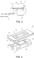
- FIG. 3 is a schematic side view of the door switch 1 when the sensor 10 is viewed in a plan view from the side of the top surface T1.
- the surface S1 of the sensor 10 and the surface S2 of the actuator 20 are disposed so as to be in contact with each other. That is, the actuator 20 is disposed on the second direction side of the sensor 10. In addition, since the display part 110 is formed on the side of the surface S1 of the sensor 10, the display part 110 and the surface S2 of the actuator 20 are in contact with each other.
- a length of the display part 110 of the sensor 10 in the first direction is defined as d1.
- a length of the actuator 20 in the first direction is defined as d2.
- the relationship between the length d1 and the length d2 can be defined as d1 > d2, for example.
- the display part 110 can be visually recognized easily.
- the opposite state of the door switch 1 can be easily determined according to the light emission of the display part 110.
- the sensor 10 and the actuator 20 are disposed flush with one side face, as shown in FIG. 2 .
- the visibility of the display part 110 can also be improved with the above configuration. In this way, it is easy to accurately dispose the door switch 1 having the display part 110 with good visibility at a desired position of the door.
- the top surface T1 of the sensor 10 and the top surface T2 of the actuator 20 are disposed so as to be flush with each other is shown as an example, but the sensor 10 may be disposed at a position where the opposite state from the actuator 20 can be detected. In other words, the disposition position and orientation are not limited.
- the sensor 10 and the actuator 20 are disposed so as to be contactable with each other, that is, when the distance between the surface S1 and the surface S2 is within a prescribed range, the sensor 10 and the actuator 20 are in the opposite state. At this time, the door switch 1 is in the closed state.
- the sensor 10 and the actuator 20 are in a non-opposite state. At this time, the door switch 1 is in the open state.
- the state in which the visibility needs to be improved is the above-mentioned open state.
- the actuator 20 overlaps the sensor 10, it is difficult to determine whether the door is in the open state or in the closed state.
- the opposite state of the door switch 1 can be easily recognized according to the light emitting state of the non-opposite region R1 of the display part 110, and the visibility is improved.
- the closed state of the door can be reliably visually recognized.
- at least a part of the display part 110 can be reliably visually recognized. Therefore, the open and close of the door can be reliably recognized.
- the space H1 in which the indirect light source 115 is formed is covered by a cover part 150.
- the cover part 150 may have any shape that covers at least the space H1.
- cover part 150 may be formed with, for example, an opaque resin as the material.
- Light from the light source 135 is the strongest in the indirect light source 115.
- the light is diffused and absorbed by a back surface of the cover part 150.
- the light diffused by the cover part 150 is guided to the display part 110.
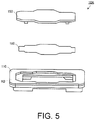
- FIG. 5 is an exploded view of a part of a sensor according to the second embodiment of the disclosure.
- the second embodiment differs from the first embodiment in the shape of a space H2 and in that a sensor 10A includes a reflection part 160 and that an indirect light source is not included.
- the other points are the same as those of the first embodiment, and descriptions of the same places are omitted.
- the sensor 10A includes the space H2.
- the reflection part 160 is fitted in the space H2, that is, the reflection part 160 is included in the space H2.
- the shape of the space H2 may be a rectangle or an ellipse and may be in any shape as long as the size and the shape of the space H2 can allow the reflection part 160 to be formed.
- the reflection part 160 reflects light from the light source 135 (not shown in FIG. 5 ), and the reflected light is guided to the display part 110.
- the display part 110 can emit light uniformly and improve illuminance.
- the opposite state of the door switch 1 can be easily recognized according to the light emitting state of the non-opposite region R1 of the display part 110, thereby improving the visibility.
- the closed state of the door can be reliably visually recognized.
- at least a part of the display part 110 can be reliably visually recognized. Therefore, the open and close of the door can be reliably recognized.
Landscapes
- Physics & Mathematics (AREA)
- General Physics & Mathematics (AREA)
- Engineering & Computer Science (AREA)
- Theoretical Computer Science (AREA)
- Optics & Photonics (AREA)
- Electromagnetism (AREA)
- Life Sciences & Earth Sciences (AREA)
- General Life Sciences & Earth Sciences (AREA)
- Geophysics (AREA)
- Switch Cases, Indication, And Locking (AREA)
- Switches That Are Operated By Magnetic Or Electric Fields (AREA)
- Switches Operated By Changes In Physical Conditions (AREA)
Abstract
Description
- The disclosure relates to a technique for providing a structure that improves visibility of a door switch.
- In a configuration disclosed in
Patent Document 1, visibility is improved by causing the periphery of a switch and a switch unit to emit light. - A switch according to a configuration disclosed in
Patent Document 2 includes a part that emits light in a plurality of parts in the configuration of the device to improve visibility. -
- [Patent Document 1] Japanese Laid-open No.
2017-98111 - [Patent Document 2] European Patent Publication No.
14192995 - However, when the configurations of
Patent Document 1 andPatent Document 2 are used, depending on the size, shape, and installation position of a signal transmitting device (such as an actuator or the like) used in combination with a sensor part, there is a concern that the part that emits light may be hidden and that visibility may be difficult to improve. - Also, particularly when used in a door switch, the sensor and the signal transmitting device are usually opposite to each other in a normal state. In this case, even if there is a place that emits light in a part of the sensor, this place is hidden by the signal transmitting device, and the visibility is difficult to improve.
- Therefore, it is an object of the disclosure to provide a door switch that improves visibility of a light emitting state.
- The door switch includes an actuator and a sensor. In addition, the door switch is installed so that, when a door is closed, a surface of the sensor and an opposite surface of the actuator are in contact with or close to each other, and when the door is open, the surface of the sensor and the opposite surface of the actuator are separated from each other.
- The actuator outputs a detection signal. A display part for indicating a reception state of the detection signal is formed on the surface of the sensor. The surface of the sensor has a non-opposite region, wherein the non-opposite region is at least a part of the display part not opposite to the opposite surface of the actuator in the reception state.
- In this configuration, even if the display part of the sensor is disposed opposite to the actuator, the display part has a part not overlapping the actuator. In this way, the visibility of the display part regarding the opposite state of the door switch is improved. Therefore, an operator can confirm the state of the sensor from any direction.
- In the door switch, the display part may be formed annularly along at least an outer edge of the surface of the sensor.
- In this configuration, the installation position of the actuator with respect to the sensor can be made flexible. Therefore, the operator can easily confirm the state of the sensor from any position.
- It is preferable that the sensor in the door switch includes a light source part. In addition, it is preferable that the display part guides light of the light source part.
- In this configuration, light of a light source part is guided, thereby further improving the visibility of the display part.
- It is preferable that the sensor in the door switch includes a light guide part for guiding the light of the light source part to the display part.
- In this configuration, even when the light source part is a point light source, the light guide part can diffuse light and allow the display part to emit light uniformly.
- It is preferable that the sensor in the door switch includes, on a display part side of the light source part or the light guide part, a cover part for preventing the light of the light source part from diffusing to outside.
- In this configuration, even when the light source part is a point light source, the cover part can hide locally bright parts and reduce unevenness of light emission.
- It is preferable that the sensor in the door switch includes a reflection part on a back surface side of the cover part.
- In this configuration, even when the light source part is a point light source, light can be further diffused and the display part can be made to emit light uniformly.
- It is preferable that the display part in the door switch is made of a resin.
- With this configuration, manufacture is easy.
- It is preferable that the cover part in the door switch is made of a resin.
- With this configuration, manufacture is easy.
- According to the disclosure, a door switch that improves visibility of a light emitting state can be provided.
-
-
FIG. 1 is a perspective view of a door switch according to the first embodiment of the disclosure. -
FIG. 2 is an exploded view of a sensor according to the first embodiment of the disclosure. -
FIG. 3 is a schematic side view of a door switch according to the first embodiment of the disclosure. -
FIG. 4 is an exploded view of a sensor according to the first embodiment of the disclosure. -
FIG. 5 is an exploded view of a part of a sensor according to the second embodiment of the disclosure. - First, an example to which the disclosure is applied will be described with reference to
FIG. 1. FIG. 1 is a schematic view of a door switch according to the first embodiment. - As shown in
FIG. 1 , thedoor switch 1 includes asensor 10 and anactuator 20. Awiring part 30 is connected to thesensor 10 and transmits a signal received by thesensor 10 to other devices. Thewiring part 30 is, for example, a connector, a cable or the like. Further, a transverse direction of thedoor switch 1 is defined as a first direction, and a longitudinal direction of thedoor switch 1 is defined as a second direction. In addition, a direction of thedoor switch 1 orthogonal to the first direction and the second direction is defined as a third direction. - First, a configuration of the
sensor 10 will be described. Thesensor 10 is formed with adisplay part 110, a backsurface display part 120, and asensor housing 140. Thesensor 10 is formed with a surface S1, a back surface B1 and side surfaces connecting the surface S1 and the back surface B1. - In addition, among the side surfaces connecting the surface S1 and the back surface B1, a surface opposite to a surface connected with the
wiring part 30 is defined as a top surface T1. - The
display part 110 is formed on the surface S1 of thesensor housing 140. The backsurface display part 120 is formed at a position corresponding to the approximate center of the back surface B1 of thesensor housing 140. - Next, a configuration of the
actuator 20 will be described. Theactuator 20 is formed with a surface S2, a back surface B2 and side surfaces connecting the surface S2 and the back surface B2. The surface S2 of theactuator 20 is the "opposite surface of the actuator" in the disclosure. - In addition, among the side surfaces connecting the surface S2 and the back surface B2, a surface on the side of the top surface T1 of the
sensor 10 is defined as a top surface T2. - More specifically, an example of the relationship between the
sensor 10 and theactuator 20 will be described below. - The
sensor 10 includes an RFID antenna (not shown) therein. In addition, theactuator 20 includes a passive IC tag (not shown) therein. - The RFID antenna transmits radio waves to the passive IC tag and receives radio waves from the passive IC tag. In this way, an opposite state between the
sensor 10 and theactuator 20 can be obtained. - Although passive RFID is shown as an example above, active RFID may be used instead. In addition, although RFID is shown as an example, the embodiments are not limited to RFID, and any configuration that can obtain the opposite state may be used.
- The
display part 110 emits light according to the opposite state of thedoor switch 1. For example, in a state where a door is open, thedisplay part 110 emits red light, and to show a state where the door is closed, thedisplay part 110 emits green light. - Next, an area SR1 of the surface S1 is compared with an area SR2 of the surface S2. The area SR1 is larger than the area SR2. Therefore, the
sensor 10 has a region where thesensor 10 is not opposite to the actuator 20 (a non-opposite region R1 in the disclosure). - A relational expression between the non-opposite region R1, the area SR1 and the area SR2 is expressed by SR1 =
R 1 + SR2. Thedisplay part 110 is disposed so as to include at least a part of the non-opposite region R1. In this way, a user can visually recognize thedisplay part 110 in the non-opposite region R1. - As described above, the opposite state can be detected by an opposite distance between the
sensor 10 and theactuator 20. - In this way, the opposite state of the
door switch 1 can be easily recognized according to a light emitting state of the non-opposite region R1 of thedisplay part 110, thereby improving the visibility. As a result, a closed state of the door can be reliably visually recognized. On the other hand, even in an open state of the door, at least a part of thedisplay part 110 can be reliably visually recognized. Therefore, the open and close of the door can be reliably recognized. - As described above,
FIG. 1 is a perspective view of the door switch according to the first embodiment of the disclosure.FIG. 2 is an exploded view of the sensor according to the first embodiment of the disclosure.FIG. 3 is a schematic side view of the door switch according to the first embodiment of the disclosure.FIG. 4 is an exploded view of the sensor according to the first embodiment of the disclosure. - A more specific configuration example will be described with reference to
FIG. 2 based on the functional configuration ofFIG. 1 described above.FIG. 2 is an exploded view showing a configuration of a part of thesensor 10. InFIG. 2 , only the main part of thesensor 10 is shown, and a part of the configuration is omitted. - The
sensor 10 is formed with thedisplay part 110, asubstrate 130, and thesensor housing 140. In addition, thedisplay part 110 and thesubstrate 130 are formed to be in contact with each other. Thesensor housing 140 covers thesubstrate 130 and thedisplay part 110 is disposed on a surface thereof. - The shape of the
display part 110 is formed annularly along an outer edge of the surface S1 of thesensor 10. In other words, thedisplay part 110 is a structure having a space H1 in the center. In the space H1, at least one indirectlight source 115 is formed. The shape of the space H1 may be a rectangle or an ellipse and is not limited to any shape as long as the size and the shape of the space H1 can allow the indirectlight source 115 to be formed. The indirectlight source 115 is connected to thedisplay part 110 by alight guide 116. A light guide part in the disclosure is a structure including the indirectlight source 115 and thelight guide 116. - The indirect
light source 115 in the disclosure does not have a function of emitting light but has a function of diffusing light received from places outside itself. - The
display part 110, the indirectlight source 115 and thelight guide 116 are made of translucent materials. Thedisplay part 110, the indirectlight source 115, and thelight guide 116 use a resin, for example, as the material. Therefore, they can be manufactured easily and at a low cost. In addition, thedisplay part 110, the indirectlight source 115 and thelight guide 116 can easily be formed integrally. - At least one
light source 135 is disposed on the side where thesubstrate 130 is in contact with thedisplay part 110. Thesubstrate 130 has a rigid shape or a flexible shape. Thelight source 135 is a point light source and is, for example, an LED. Since thelight source 135 is an LED, thelight source 135 can be formed relatively inexpensively, and power consumption can be reduced. - The
sensor housing 140 includes the backsurface display part 120 at a position corresponding to the approximate center. In addition, it is sufficient that the backsurface display part 120 is formed on the back surface B1, and the formation position is not limited. - As described above, the
display part 110 is formed so as to overlap thesubstrate 130 when viewed in a plan view. Further, it is preferable that the indirectlight source 115 and thelight source 135 are formed to be in contact with each other. With this configuration, light from thelight source 135 can directly enter the indirectlight source 115, and the light can be diffused to thedisplay part 110 via the indirectlight source 115 and thelight guide 116. In this way, the light guide efficiency is improved. - A detailed positional relationship of the
sensor 10 and theactuator 20 in contact with each other will be described with reference toFIG. 3. FIG. 3 is a schematic side view of thedoor switch 1 when thesensor 10 is viewed in a plan view from the side of the top surface T1. - The surface S1 of the
sensor 10 and the surface S2 of theactuator 20 are disposed so as to be in contact with each other. That is, theactuator 20 is disposed on the second direction side of thesensor 10. In addition, since thedisplay part 110 is formed on the side of the surface S1 of thesensor 10, thedisplay part 110 and the surface S2 of theactuator 20 are in contact with each other. - A length of the
display part 110 of thesensor 10 in the first direction is defined as d1. Similarly, a length of theactuator 20 in the first direction is defined as d2. The relationship between the length d1 and the length d2 can be defined as d1 > d2, for example. - Thus, for example, even if the
sensor 10 is fixed and theactuator 20 is in contact with any position of thedisplay part 110 in the first direction, thedisplay part 110 can be visually recognized easily. - As shown in
FIG. 2 , since thedisplay part 110 is formed so as to cover the outer edge of thesensor 10, the opposite state of thedoor switch 1 can be easily determined according to the light emission of thedisplay part 110. - In addition, in a general door switch, the
sensor 10 and theactuator 20 are disposed flush with one side face, as shown inFIG. 2 . In this case, the visibility of thedisplay part 110 can also be improved with the above configuration. In this way, it is easy to accurately dispose thedoor switch 1 having thedisplay part 110 with good visibility at a desired position of the door. - As shown in
FIG. 1 , a case in which the top surface T1 of thesensor 10 and the top surface T2 of theactuator 20 are disposed so as to be flush with each other is shown as an example, but thesensor 10 may be disposed at a position where the opposite state from theactuator 20 can be detected. In other words, the disposition position and orientation are not limited. - In addition, when the surface S1 of the
sensor 10 and the surface S2 of theactuator 20 are disposed so as to be contactable with each other, that is, when the distance between the surface S1 and the surface S2 is within a prescribed range, thesensor 10 and theactuator 20 are in the opposite state. At this time, thedoor switch 1 is in the closed state. - Further, when the distance between the surface S1 of the
sensor 10 and the surface S2 of theactuator 20 is out of the prescribed range, thesensor 10 and theactuator 20 are in a non-opposite state. At this time, thedoor switch 1 is in the open state. - In the disclosure, the state in which the visibility needs to be improved is the above-mentioned open state. For example, when a part of the
actuator 20 overlaps thesensor 10, it is difficult to determine whether the door is in the open state or in the closed state. - However, by using the above configuration, the opposite state of the
door switch 1 can be easily recognized according to the light emitting state of the non-opposite region R1 of thedisplay part 110, and the visibility is improved. As a result, the closed state of the door can be reliably visually recognized. On the other hand, even in the open state of the door, at least a part of thedisplay part 110 can be reliably visually recognized. Therefore, the open and close of the door can be reliably recognized. - With reference to
FIG. 4 , a light emitting structure for further improving the visibility in thedisplay part 110 of thesensor 10 will be described. As shown inFIG. 4 , the space H1 in which the indirectlight source 115 is formed is covered by acover part 150. Thecover part 150 may have any shape that covers at least the space H1. - In addition, the
cover part 150 may be formed with, for example, an opaque resin as the material. - Light from the
light source 135 is the strongest in the indirectlight source 115. The light is diffused and absorbed by a back surface of thecover part 150. The light diffused by thecover part 150 is guided to thedisplay part 110. Also, by providing thecover part 150, there is an effect that strong light spots of the light integrated by the indirectlight source 115 can be hidden. As a result, unevenness of the luminance of the surface S1 of thesensor 10 is reduced, and thedisplay part 110 emits light uniformly, and the illuminance is improved. - Next, an overview of a door switch according to the second embodiment will be described with reference to
FIG. 5. FIG. 5 is an exploded view of a part of a sensor according to the second embodiment of the disclosure. - The second embodiment differs from the first embodiment in the shape of a space H2 and in that a
sensor 10A includes areflection part 160 and that an indirect light source is not included. The other points are the same as those of the first embodiment, and descriptions of the same places are omitted. - The
sensor 10A includes the space H2. Thereflection part 160 is fitted in the space H2, that is, thereflection part 160 is included in the space H2. - In addition, the shape of the space H2 may be a rectangle or an ellipse and may be in any shape as long as the size and the shape of the space H2 can allow the
reflection part 160 to be formed. - Therefore, the
reflection part 160 reflects light from the light source 135 (not shown inFIG. 5 ), and the reflected light is guided to thedisplay part 110. - As a result, the
display part 110 can emit light uniformly and improve illuminance. - Even in this configuration, the opposite state of the
door switch 1 can be easily recognized according to the light emitting state of the non-opposite region R1 of thedisplay part 110, thereby improving the visibility. As a result, the closed state of the door can be reliably visually recognized. On the other hand, even in the open state of the door, at least a part of thedisplay part 110 can be reliably visually recognized. Therefore, the open and close of the door can be reliably recognized. - In this embodiment, a structure without an indirect light source included therein has been described. However, the same effects can be achieved even with a structure including an indirect light source.
-
- B1, B2: Back surface
- d1, d2: Length
- H1, H2: Space
- R1: Non-opposite region
- S1, S2: Surface
- SR1, SR2: Area
- 1: Door switch
- 10, 10A: Sensor
- 20: Actuator
- 30: Wiring part
- 110: Display part
- 115: Indirect light source
- 116: Light guide
- 120: Back surface display part
- 130: Substrate
- 135: Light source
- 140: Sensor housing
- 150: Cover part
- 160: Reflection part
Claims (8)
- A door switch (1) comprising an actuator (20) and a sensor (10, 10A), wherein
the door switch (1) is installed so that when a door is closed, a surface (S1) of the sensor (10, 10A) and an opposite surface (S2) of the actuator (20) are in contact with or close to each other, and
when the door is open, the surface (S1) of the sensor (10, 10A) and the opposite surface (S2) of the actuator (20) are separated from each other,
the actuator (20) outputs a detection signal,
a display part (110) for indicating a reception state of the detection signal is formed on the surface (S1) of the sensor (10, 10A), and
the surface (S1) of the sensor (10, 10A) has a non-opposite region (R1), wherein the non-opposite region (R1) is at least a part of the display part (110) not opposite to the opposite surface (S2) of the actuator (20) in the reception state. - The door switch (1) according to claim 1, wherein the display part (110) is formed annularly along at least an outer edge of the surface (S1) of the sensor (10, 10A).
- The door switch (1) according to claim 1 or claim 2, wherein the sensor (10, 10A) comprises a light source part (135) inside, and the display part (110) guides light of the light source part (135).
- The door switch (1) according to claim 3, wherein the sensor (10, 10A) comprises a light guide part for guiding the light of the light source part (135) to the display part (110).
- The door switch (1) according to claim 4, wherein the sensor (10, 10A) comprises, on a display part (110) side of the light source part (135) or the light guide part, a cover part (150) for preventing the light of the light source part (135) from diffusing to outside.
- The door switch (1) according to claim 5, wherein the sensor (10A) comprises a reflection part (160) on a back surface (S1) side of the cover part (150).
- The door switch (1) according to any one of claims 1 to 6, wherein the display part (110) is made of a resin.
- The door switch (1) according to claim 5 or claim 6, wherein the cover part (150) is made of a resin.
Applications Claiming Priority (1)
| Application Number | Priority Date | Filing Date | Title |
|---|---|---|---|
| JP2018019986A JP6915558B2 (en) | 2018-02-07 | 2018-02-07 | Door switch |
Publications (2)
| Publication Number | Publication Date |
|---|---|
| EP3525349A1 true EP3525349A1 (en) | 2019-08-14 |
| EP3525349B1 EP3525349B1 (en) | 2021-04-07 |
Family
ID=64316373
Family Applications (1)
| Application Number | Title | Priority Date | Filing Date |
|---|---|---|---|
| EP18206213.3A Active EP3525349B1 (en) | 2018-02-07 | 2018-11-14 | Door switch |
Country Status (5)
| Country | Link |
|---|---|
| US (1) | US10657778B2 (en) |
| EP (1) | EP3525349B1 (en) |
| JP (1) | JP6915558B2 (en) |
| KR (1) | KR102104475B1 (en) |
| CN (1) | CN110118997B (en) |
Families Citing this family (3)
| Publication number | Priority date | Publication date | Assignee | Title |
|---|---|---|---|---|
| JP7411907B2 (en) | 2020-01-24 | 2024-01-12 | パナソニックIpマネジメント株式会社 | Device with safety switch and door |
| JP2023007787A (en) | 2021-07-02 | 2023-01-19 | パナソニックIpマネジメント株式会社 | Fixture, actuator with fixture, and detection switch |
| JP2023007786A (en) | 2021-07-02 | 2023-01-19 | パナソニックIpマネジメント株式会社 | Fixture, actuator with fixture, and detection switch |
Citations (1)
| Publication number | Priority date | Publication date | Assignee | Title |
|---|---|---|---|---|
| JP2017098111A (en) | 2015-11-25 | 2017-06-01 | 富士電機機器制御株式会社 | Illumination unit for switch and switch |
Family Cites Families (9)
| Publication number | Priority date | Publication date | Assignee | Title |
|---|---|---|---|---|
| JP2002343210A (en) * | 2001-05-17 | 2002-11-29 | Koyo Electronics Ind Co Ltd | Attachment structure for sensor switch |
| JP2003223683A (en) * | 2002-01-29 | 2003-08-08 | Nittan Co Ltd | Detection device, detection system, and output voltage value registration method |
| US8773263B2 (en) * | 2011-09-01 | 2014-07-08 | Ecolink Intelligent Technology, Inc. | Security apparatus and method |
| US9118220B2 (en) * | 2012-07-02 | 2015-08-25 | Ecolink Intelligent Technology, Inc. | Method and apparatus for providing energy device and system status |
| JP6079363B2 (en) | 2013-03-27 | 2017-02-15 | 日本電気株式会社 | Connection status monitoring system |
| US9349260B2 (en) | 2013-11-13 | 2016-05-24 | Rockwell Automation Technologies, Inc. | Sensor device with enhanced light guide visualization and related methods |
| CN204808517U (en) * | 2015-07-24 | 2015-11-25 | 江西智能无限物联科技有限公司 | Intelligence door and window sensor |
| KR20170098111A (en) | 2016-02-19 | 2017-08-29 | 삼성전자주식회사 | Method for controlling display using sensor data and electronic device thereof |
| US10203084B1 (en) * | 2017-12-11 | 2019-02-12 | Ecolink Intelligent Technology, Inc. | Illumination feature for electronic devices |
-
2018
- 2018-02-07 JP JP2018019986A patent/JP6915558B2/en active Active
- 2018-11-13 KR KR1020180138871A patent/KR102104475B1/en active Active
- 2018-11-14 EP EP18206213.3A patent/EP3525349B1/en active Active
- 2018-11-14 CN CN201811351139.5A patent/CN110118997B/en active Active
- 2018-11-14 US US16/190,147 patent/US10657778B2/en active Active
Patent Citations (1)
| Publication number | Priority date | Publication date | Assignee | Title |
|---|---|---|---|---|
| JP2017098111A (en) | 2015-11-25 | 2017-06-01 | 富士電機機器制御株式会社 | Illumination unit for switch and switch |
Non-Patent Citations (2)
| Title |
|---|
| ANONYMOUS: "Door/Window Sensor", 17 June 2015 (2015-06-17), XP055583180, Retrieved from the Internet <URL:https://www.zipato.com/wp-content/uploads/2015/07/vs-zd2102-Zipato-DoorWindow-Sensor-Data-Sheet.pdf> [retrieved on 20190424] * |
| CHRISTOPHE PAYS: "Manuel d'instruction SERIE XORF capteur de sécurité COMITRONIC -BTI AUTRES PRODUCTIONS : BOUTON TACTILE FORCE 0 ET IP 69K OTHER PRODUCTIONS: TOUCH PUSH BUTTON FORCE 0 AND IP 69K COMITRONIC-BTI, LEADER DU CAPTEUR DE SÉCURITÉ AUTONOME COMITRONIC-BTI, AUTONOMOUS SAFETY SENSOR LEADER", 16 July 2018 (2018-07-16), pages 1 - 8, XP055583132, Retrieved from the Internet <URL:https://comitronic-bti.eu/documentations/datasheet/#186-rfid-datasheet-datasheet-p2> [retrieved on 20190424] * |
Also Published As
| Publication number | Publication date |
|---|---|
| US20190244489A1 (en) | 2019-08-08 |
| US10657778B2 (en) | 2020-05-19 |
| KR102104475B1 (en) | 2020-04-24 |
| JP2019139877A (en) | 2019-08-22 |
| KR20190095865A (en) | 2019-08-16 |
| CN110118997A (en) | 2019-08-13 |
| CN110118997B (en) | 2021-06-11 |
| EP3525349B1 (en) | 2021-04-07 |
| JP6915558B2 (en) | 2021-08-04 |
Similar Documents
| Publication | Publication Date | Title |
|---|---|---|
| US10657778B2 (en) | Door switch | |
| CN109061946B (en) | Display components and electronic equipment | |
| US8894242B2 (en) | Electronic device casing with a water inhibitor | |
| EP3846072A1 (en) | Under-screen fingerprint recognition apparatus and electronic device | |
| US20070019433A1 (en) | Shared light pipe for a message indicator and light sensor | |
| KR20080110118A (en) | Electronic device with display | |
| US20090058306A1 (en) | Blacklight unit and display device | |
| US20110234940A1 (en) | Liquid crystal display device | |
| US7001061B2 (en) | Illumination apparatus with housing frame including cut-out portion for FPC | |
| US8579449B2 (en) | Pointer type measuring instrument | |
| JP5279011B2 (en) | Lighting device and electronic device | |
| JP6779713B2 (en) | In-vehicle antenna device | |
| US8608359B2 (en) | Mobile terminal having a light source and a light reflector within the mobile terminal to illuminate the mobile terminal | |
| EP2237102A1 (en) | Liquid crystal display device | |
| EP3525350B1 (en) | Door switch | |
| JP2001184926A (en) | Planar lighting device | |
| JP2006323615A (en) | Light indicator structure | |
| CN224219674U (en) | Mirror body and makeup mirror | |
| JP6327068B2 (en) | Display device | |
| KR102341530B1 (en) | Sensor | |
| JP3372630B2 (en) | Portable communication equipment | |
| US20120063170A1 (en) | Mobile terminal device | |
| JP7001311B2 (en) | Electrostatic sensor type surface illuminated switch with light emitting member with electrostatic sensor pattern | |
| JP2026059048A (en) | Communication device and object detection device | |
| JP2026043982A (en) | Lighting device, luminaire and wireless module |
Legal Events
| Date | Code | Title | Description |
|---|---|---|---|
| PUAI | Public reference made under article 153(3) epc to a published international application that has entered the european phase |
Free format text: ORIGINAL CODE: 0009012 |
|
| STAA | Information on the status of an ep patent application or granted ep patent |
Free format text: STATUS: REQUEST FOR EXAMINATION WAS MADE |
|
| 17P | Request for examination filed |
Effective date: 20181114 |
|
| AK | Designated contracting states |
Kind code of ref document: A1 Designated state(s): AL AT BE BG CH CY CZ DE DK EE ES FI FR GB GR HR HU IE IS IT LI LT LU LV MC MK MT NL NO PL PT RO RS SE SI SK SM TR |
|
| AX | Request for extension of the european patent |
Extension state: BA ME |
|
| RBV | Designated contracting states (corrected) |
Designated state(s): AL AT BE BG CH CY CZ DE DK EE ES FI FR GB GR HR HU IE IS IT LI LT LU LV MC MK MT NL NO PL PT RO RS SE SI SK SM TR |
|
| GRAP | Despatch of communication of intention to grant a patent |
Free format text: ORIGINAL CODE: EPIDOSNIGR1 |
|
| STAA | Information on the status of an ep patent application or granted ep patent |
Free format text: STATUS: GRANT OF PATENT IS INTENDED |
|
| INTG | Intention to grant announced |
Effective date: 20201215 |
|
| GRAS | Grant fee paid |
Free format text: ORIGINAL CODE: EPIDOSNIGR3 |
|
| GRAA | (expected) grant |
Free format text: ORIGINAL CODE: 0009210 |
|
| STAA | Information on the status of an ep patent application or granted ep patent |
Free format text: STATUS: THE PATENT HAS BEEN GRANTED |
|
| AK | Designated contracting states |
Kind code of ref document: B1 Designated state(s): AL AT BE BG CH CY CZ DE DK EE ES FI FR GB GR HR HU IE IS IT LI LT LU LV MC MK MT NL NO PL PT RO RS SE SI SK SM TR |
|
| REG | Reference to a national code |
Ref country code: GB Ref legal event code: FG4D |
|
| REG | Reference to a national code |
Ref country code: AT Ref legal event code: REF Ref document number: 1381001 Country of ref document: AT Kind code of ref document: T Effective date: 20210415 Ref country code: CH Ref legal event code: EP |
|
| REG | Reference to a national code |
Ref country code: DE Ref legal event code: R096 Ref document number: 602018015095 Country of ref document: DE |
|
| REG | Reference to a national code |
Ref country code: IE Ref legal event code: FG4D |
|
| REG | Reference to a national code |
Ref country code: LT Ref legal event code: MG9D |
|
| REG | Reference to a national code |
Ref country code: NL Ref legal event code: MP Effective date: 20210407 Ref country code: AT Ref legal event code: MK05 Ref document number: 1381001 Country of ref document: AT Kind code of ref document: T Effective date: 20210407 |
|
| PG25 | Lapsed in a contracting state [announced via postgrant information from national office to epo] |
Ref country code: LT Free format text: LAPSE BECAUSE OF FAILURE TO SUBMIT A TRANSLATION OF THE DESCRIPTION OR TO PAY THE FEE WITHIN THE PRESCRIBED TIME-LIMIT Effective date: 20210407 Ref country code: HR Free format text: LAPSE BECAUSE OF FAILURE TO SUBMIT A TRANSLATION OF THE DESCRIPTION OR TO PAY THE FEE WITHIN THE PRESCRIBED TIME-LIMIT Effective date: 20210407 Ref country code: FI Free format text: LAPSE BECAUSE OF FAILURE TO SUBMIT A TRANSLATION OF THE DESCRIPTION OR TO PAY THE FEE WITHIN THE PRESCRIBED TIME-LIMIT Effective date: 20210407 Ref country code: NL Free format text: LAPSE BECAUSE OF FAILURE TO SUBMIT A TRANSLATION OF THE DESCRIPTION OR TO PAY THE FEE WITHIN THE PRESCRIBED TIME-LIMIT Effective date: 20210407 Ref country code: BG Free format text: LAPSE BECAUSE OF FAILURE TO SUBMIT A TRANSLATION OF THE DESCRIPTION OR TO PAY THE FEE WITHIN THE PRESCRIBED TIME-LIMIT Effective date: 20210707 Ref country code: AT Free format text: LAPSE BECAUSE OF FAILURE TO SUBMIT A TRANSLATION OF THE DESCRIPTION OR TO PAY THE FEE WITHIN THE PRESCRIBED TIME-LIMIT Effective date: 20210407 |
|
| PG25 | Lapsed in a contracting state [announced via postgrant information from national office to epo] |
Ref country code: SE Free format text: LAPSE BECAUSE OF FAILURE TO SUBMIT A TRANSLATION OF THE DESCRIPTION OR TO PAY THE FEE WITHIN THE PRESCRIBED TIME-LIMIT Effective date: 20210407 Ref country code: RS Free format text: LAPSE BECAUSE OF FAILURE TO SUBMIT A TRANSLATION OF THE DESCRIPTION OR TO PAY THE FEE WITHIN THE PRESCRIBED TIME-LIMIT Effective date: 20210407 Ref country code: PT Free format text: LAPSE BECAUSE OF FAILURE TO SUBMIT A TRANSLATION OF THE DESCRIPTION OR TO PAY THE FEE WITHIN THE PRESCRIBED TIME-LIMIT Effective date: 20210809 Ref country code: PL Free format text: LAPSE BECAUSE OF FAILURE TO SUBMIT A TRANSLATION OF THE DESCRIPTION OR TO PAY THE FEE WITHIN THE PRESCRIBED TIME-LIMIT Effective date: 20210407 Ref country code: NO Free format text: LAPSE BECAUSE OF FAILURE TO SUBMIT A TRANSLATION OF THE DESCRIPTION OR TO PAY THE FEE WITHIN THE PRESCRIBED TIME-LIMIT Effective date: 20210707 Ref country code: LV Free format text: LAPSE BECAUSE OF FAILURE TO SUBMIT A TRANSLATION OF THE DESCRIPTION OR TO PAY THE FEE WITHIN THE PRESCRIBED TIME-LIMIT Effective date: 20210407 Ref country code: GR Free format text: LAPSE BECAUSE OF FAILURE TO SUBMIT A TRANSLATION OF THE DESCRIPTION OR TO PAY THE FEE WITHIN THE PRESCRIBED TIME-LIMIT Effective date: 20210708 Ref country code: IS Free format text: LAPSE BECAUSE OF FAILURE TO SUBMIT A TRANSLATION OF THE DESCRIPTION OR TO PAY THE FEE WITHIN THE PRESCRIBED TIME-LIMIT Effective date: 20210807 |
|
| REG | Reference to a national code |
Ref country code: DE Ref legal event code: R097 Ref document number: 602018015095 Country of ref document: DE |
|
| PG25 | Lapsed in a contracting state [announced via postgrant information from national office to epo] |
Ref country code: ES Free format text: LAPSE BECAUSE OF FAILURE TO SUBMIT A TRANSLATION OF THE DESCRIPTION OR TO PAY THE FEE WITHIN THE PRESCRIBED TIME-LIMIT Effective date: 20210407 Ref country code: EE Free format text: LAPSE BECAUSE OF FAILURE TO SUBMIT A TRANSLATION OF THE DESCRIPTION OR TO PAY THE FEE WITHIN THE PRESCRIBED TIME-LIMIT Effective date: 20210407 Ref country code: SM Free format text: LAPSE BECAUSE OF FAILURE TO SUBMIT A TRANSLATION OF THE DESCRIPTION OR TO PAY THE FEE WITHIN THE PRESCRIBED TIME-LIMIT Effective date: 20210407 Ref country code: SK Free format text: LAPSE BECAUSE OF FAILURE TO SUBMIT A TRANSLATION OF THE DESCRIPTION OR TO PAY THE FEE WITHIN THE PRESCRIBED TIME-LIMIT Effective date: 20210407 Ref country code: DK Free format text: LAPSE BECAUSE OF FAILURE TO SUBMIT A TRANSLATION OF THE DESCRIPTION OR TO PAY THE FEE WITHIN THE PRESCRIBED TIME-LIMIT Effective date: 20210407 Ref country code: CZ Free format text: LAPSE BECAUSE OF FAILURE TO SUBMIT A TRANSLATION OF THE DESCRIPTION OR TO PAY THE FEE WITHIN THE PRESCRIBED TIME-LIMIT Effective date: 20210407 Ref country code: RO Free format text: LAPSE BECAUSE OF FAILURE TO SUBMIT A TRANSLATION OF THE DESCRIPTION OR TO PAY THE FEE WITHIN THE PRESCRIBED TIME-LIMIT Effective date: 20210407 |
|
| PLBE | No opposition filed within time limit |
Free format text: ORIGINAL CODE: 0009261 |
|
| STAA | Information on the status of an ep patent application or granted ep patent |
Free format text: STATUS: NO OPPOSITION FILED WITHIN TIME LIMIT |
|
| 26N | No opposition filed |
Effective date: 20220110 |
|
| PG25 | Lapsed in a contracting state [announced via postgrant information from national office to epo] |
Ref country code: IS Free format text: LAPSE BECAUSE OF FAILURE TO SUBMIT A TRANSLATION OF THE DESCRIPTION OR TO PAY THE FEE WITHIN THE PRESCRIBED TIME-LIMIT Effective date: 20210807 Ref country code: AL Free format text: LAPSE BECAUSE OF FAILURE TO SUBMIT A TRANSLATION OF THE DESCRIPTION OR TO PAY THE FEE WITHIN THE PRESCRIBED TIME-LIMIT Effective date: 20210407 |
|
| PG25 | Lapsed in a contracting state [announced via postgrant information from national office to epo] |
Ref country code: MC Free format text: LAPSE BECAUSE OF FAILURE TO SUBMIT A TRANSLATION OF THE DESCRIPTION OR TO PAY THE FEE WITHIN THE PRESCRIBED TIME-LIMIT Effective date: 20210407 |
|
| REG | Reference to a national code |
Ref country code: CH Ref legal event code: PL |
|
| PG25 | Lapsed in a contracting state [announced via postgrant information from national office to epo] |
Ref country code: LU Free format text: LAPSE BECAUSE OF NON-PAYMENT OF DUE FEES Effective date: 20211114 Ref country code: IT Free format text: LAPSE BECAUSE OF FAILURE TO SUBMIT A TRANSLATION OF THE DESCRIPTION OR TO PAY THE FEE WITHIN THE PRESCRIBED TIME-LIMIT Effective date: 20210407 Ref country code: BE Free format text: LAPSE BECAUSE OF NON-PAYMENT OF DUE FEES Effective date: 20211130 |
|
| REG | Reference to a national code |
Ref country code: BE Ref legal event code: MM Effective date: 20211130 |
|
| PG25 | Lapsed in a contracting state [announced via postgrant information from national office to epo] |
Ref country code: LI Free format text: LAPSE BECAUSE OF NON-PAYMENT OF DUE FEES Effective date: 20211130 Ref country code: CH Free format text: LAPSE BECAUSE OF NON-PAYMENT OF DUE FEES Effective date: 20211130 |
|
| PG25 | Lapsed in a contracting state [announced via postgrant information from national office to epo] |
Ref country code: IE Free format text: LAPSE BECAUSE OF NON-PAYMENT OF DUE FEES Effective date: 20211114 |
|
| PG25 | Lapsed in a contracting state [announced via postgrant information from national office to epo] |
Ref country code: FR Free format text: LAPSE BECAUSE OF NON-PAYMENT OF DUE FEES Effective date: 20211130 |
|
| PG25 | Lapsed in a contracting state [announced via postgrant information from national office to epo] |
Ref country code: CY Free format text: LAPSE BECAUSE OF FAILURE TO SUBMIT A TRANSLATION OF THE DESCRIPTION OR TO PAY THE FEE WITHIN THE PRESCRIBED TIME-LIMIT Effective date: 20210407 |
|
| GBPC | Gb: european patent ceased through non-payment of renewal fee |
Effective date: 20221114 |
|
| PG25 | Lapsed in a contracting state [announced via postgrant information from national office to epo] |
Ref country code: HU Free format text: LAPSE BECAUSE OF FAILURE TO SUBMIT A TRANSLATION OF THE DESCRIPTION OR TO PAY THE FEE WITHIN THE PRESCRIBED TIME-LIMIT; INVALID AB INITIO Effective date: 20181114 |
|
| PG25 | Lapsed in a contracting state [announced via postgrant information from national office to epo] |
Ref country code: GB Free format text: LAPSE BECAUSE OF NON-PAYMENT OF DUE FEES Effective date: 20221114 |
|
| PG25 | Lapsed in a contracting state [announced via postgrant information from national office to epo] |
Ref country code: MK Free format text: LAPSE BECAUSE OF FAILURE TO SUBMIT A TRANSLATION OF THE DESCRIPTION OR TO PAY THE FEE WITHIN THE PRESCRIBED TIME-LIMIT Effective date: 20210407 |
|
| PG25 | Lapsed in a contracting state [announced via postgrant information from national office to epo] |
Ref country code: TR Free format text: LAPSE BECAUSE OF FAILURE TO SUBMIT A TRANSLATION OF THE DESCRIPTION OR TO PAY THE FEE WITHIN THE PRESCRIBED TIME-LIMIT Effective date: 20210407 |
|
| PG25 | Lapsed in a contracting state [announced via postgrant information from national office to epo] |
Ref country code: MT Free format text: LAPSE BECAUSE OF FAILURE TO SUBMIT A TRANSLATION OF THE DESCRIPTION OR TO PAY THE FEE WITHIN THE PRESCRIBED TIME-LIMIT Effective date: 20210407 |
|
| PGFP | Annual fee paid to national office [announced via postgrant information from national office to epo] |
Ref country code: DE Payment date: 20251118 Year of fee payment: 8 |