EP3524351A1 - Biomarker detection apparatus - Google Patents
Biomarker detection apparatus Download PDFInfo
- Publication number
- EP3524351A1 EP3524351A1 EP19156535.7A EP19156535A EP3524351A1 EP 3524351 A1 EP3524351 A1 EP 3524351A1 EP 19156535 A EP19156535 A EP 19156535A EP 3524351 A1 EP3524351 A1 EP 3524351A1
- Authority
- EP
- European Patent Office
- Prior art keywords
- sample
- nanoentities
- radiation
- binding
- nanostructured surface
- Prior art date
- Legal status (The legal status is an assumption and is not a legal conclusion. Google has not performed a legal analysis and makes no representation as to the accuracy of the status listed.)
- Pending
Links
Images


Classifications
-
- G—PHYSICS
- G01—MEASURING; TESTING
- G01N—INVESTIGATING OR ANALYSING MATERIALS BY DETERMINING THEIR CHEMICAL OR PHYSICAL PROPERTIES
- G01N21/00—Investigating or analysing materials by the use of optical means, i.e. using sub-millimetre waves, infrared, visible or ultraviolet light
- G01N21/17—Systems in which incident light is modified in accordance with the properties of the material investigated
- G01N21/55—Specular reflectivity
- G01N21/552—Attenuated total reflection
- G01N21/553—Attenuated total reflection and using surface plasmons
- G01N21/554—Attenuated total reflection and using surface plasmons detecting the surface plasmon resonance of nanostructured metals, e.g. localised surface plasmon resonance
-
- B—PERFORMING OPERATIONS; TRANSPORTING
- B01—PHYSICAL OR CHEMICAL PROCESSES OR APPARATUS IN GENERAL
- B01L—CHEMICAL OR PHYSICAL LABORATORY APPARATUS FOR GENERAL USE
- B01L3/00—Containers or dishes for laboratory use, e.g. laboratory glassware; Droppers
- B01L3/50—Containers for the purpose of retaining a material to be analysed, e.g. test tubes
- B01L3/502—Containers for the purpose of retaining a material to be analysed, e.g. test tubes with fluid transport, e.g. in multi-compartment structures
- B01L3/5027—Containers for the purpose of retaining a material to be analysed, e.g. test tubes with fluid transport, e.g. in multi-compartment structures by integrated microfluidic structures, i.e. dimensions of channels and chambers are such that surface tension forces are important, e.g. lab-on-a-chip
- B01L3/502715—Containers for the purpose of retaining a material to be analysed, e.g. test tubes with fluid transport, e.g. in multi-compartment structures by integrated microfluidic structures, i.e. dimensions of channels and chambers are such that surface tension forces are important, e.g. lab-on-a-chip characterised by interfacing components, e.g. fluidic, electrical, optical or mechanical interfaces
-
- G—PHYSICS
- G01—MEASURING; TESTING
- G01N—INVESTIGATING OR ANALYSING MATERIALS BY DETERMINING THEIR CHEMICAL OR PHYSICAL PROPERTIES
- G01N1/00—Sampling; Preparing specimens for investigation
- G01N1/28—Preparing specimens for investigation including physical details of (bio-)chemical methods covered elsewhere, e.g. G01N33/50, C12Q
- G01N1/38—Diluting, dispersing or mixing samples
-
- G—PHYSICS
- G01—MEASURING; TESTING
- G01N—INVESTIGATING OR ANALYSING MATERIALS BY DETERMINING THEIR CHEMICAL OR PHYSICAL PROPERTIES
- G01N1/00—Sampling; Preparing specimens for investigation
- G01N1/28—Preparing specimens for investigation including physical details of (bio-)chemical methods covered elsewhere, e.g. G01N33/50, C12Q
- G01N1/40—Concentrating samples
- G01N1/4077—Concentrating samples by other techniques involving separation of suspended solids
-
- G—PHYSICS
- G01—MEASURING; TESTING
- G01N—INVESTIGATING OR ANALYSING MATERIALS BY DETERMINING THEIR CHEMICAL OR PHYSICAL PROPERTIES
- G01N21/00—Investigating or analysing materials by the use of optical means, i.e. using sub-millimetre waves, infrared, visible or ultraviolet light
- G01N21/17—Systems in which incident light is modified in accordance with the properties of the material investigated
- G01N21/21—Polarisation-affecting properties
-
- G—PHYSICS
- G01—MEASURING; TESTING
- G01N—INVESTIGATING OR ANALYSING MATERIALS BY DETERMINING THEIR CHEMICAL OR PHYSICAL PROPERTIES
- G01N33/00—Investigating or analysing materials by specific methods not covered by groups G01N1/00 - G01N31/00
- G01N33/48—Biological material, e.g. blood, urine; Haemocytometers
- G01N33/50—Chemical analysis of biological material, e.g. blood, urine; Testing involving biospecific ligand binding methods; Immunological testing
- G01N33/53—Immunoassay; Biospecific binding assay; Materials therefor
- G01N33/543—Immunoassay; Biospecific binding assay; Materials therefor with an insoluble carrier for immobilising immunochemicals
- G01N33/54366—Apparatus specially adapted for solid-phase testing
- G01N33/54373—Apparatus specially adapted for solid-phase testing involving physiochemical end-point determination, e.g. wave-guides, FETS, gratings
-
- B—PERFORMING OPERATIONS; TRANSPORTING
- B01—PHYSICAL OR CHEMICAL PROCESSES OR APPARATUS IN GENERAL
- B01L—CHEMICAL OR PHYSICAL LABORATORY APPARATUS FOR GENERAL USE
- B01L2200/00—Solutions for specific problems relating to chemical or physical laboratory apparatus
- B01L2200/10—Integrating sample preparation and analysis in single entity, e.g. lab-on-a-chip concept
-
- B—PERFORMING OPERATIONS; TRANSPORTING
- B01—PHYSICAL OR CHEMICAL PROCESSES OR APPARATUS IN GENERAL
- B01L—CHEMICAL OR PHYSICAL LABORATORY APPARATUS FOR GENERAL USE
- B01L2300/00—Additional constructional details
- B01L2300/06—Auxiliary integrated devices, integrated components
- B01L2300/0627—Sensor or part of a sensor is integrated
- B01L2300/0654—Lenses; Optical fibres
-
- B—PERFORMING OPERATIONS; TRANSPORTING
- B01—PHYSICAL OR CHEMICAL PROCESSES OR APPARATUS IN GENERAL
- B01L—CHEMICAL OR PHYSICAL LABORATORY APPARATUS FOR GENERAL USE
- B01L2300/00—Additional constructional details
- B01L2300/08—Geometry, shape and general structure
- B01L2300/0809—Geometry, shape and general structure rectangular shaped
- B01L2300/0816—Cards, e.g. flat sample carriers usually with flow in two horizontal directions
-
- B—PERFORMING OPERATIONS; TRANSPORTING
- B01—PHYSICAL OR CHEMICAL PROCESSES OR APPARATUS IN GENERAL
- B01L—CHEMICAL OR PHYSICAL LABORATORY APPARATUS FOR GENERAL USE
- B01L2300/00—Additional constructional details
- B01L2300/08—Geometry, shape and general structure
- B01L2300/0809—Geometry, shape and general structure rectangular shaped
- B01L2300/0819—Microarrays; Biochips
-
- B—PERFORMING OPERATIONS; TRANSPORTING
- B01—PHYSICAL OR CHEMICAL PROCESSES OR APPARATUS IN GENERAL
- B01L—CHEMICAL OR PHYSICAL LABORATORY APPARATUS FOR GENERAL USE
- B01L2300/00—Additional constructional details
- B01L2300/08—Geometry, shape and general structure
- B01L2300/0861—Configuration of multiple channels and/or chambers in a single devices
- B01L2300/0864—Configuration of multiple channels and/or chambers in a single devices comprising only one inlet and multiple receiving wells, e.g. for separation, splitting
-
- B—PERFORMING OPERATIONS; TRANSPORTING
- B01—PHYSICAL OR CHEMICAL PROCESSES OR APPARATUS IN GENERAL
- B01L—CHEMICAL OR PHYSICAL LABORATORY APPARATUS FOR GENERAL USE
- B01L2300/00—Additional constructional details
- B01L2300/08—Geometry, shape and general structure
- B01L2300/0861—Configuration of multiple channels and/or chambers in a single devices
- B01L2300/0867—Multiple inlets and one sample wells, e.g. mixing, dilution
-
- G—PHYSICS
- G01—MEASURING; TESTING
- G01N—INVESTIGATING OR ANALYSING MATERIALS BY DETERMINING THEIR CHEMICAL OR PHYSICAL PROPERTIES
- G01N1/00—Sampling; Preparing specimens for investigation
- G01N1/28—Preparing specimens for investigation including physical details of (bio-)chemical methods covered elsewhere, e.g. G01N33/50, C12Q
- G01N1/40—Concentrating samples
- G01N1/4077—Concentrating samples by other techniques involving separation of suspended solids
- G01N2001/4088—Concentrating samples by other techniques involving separation of suspended solids filtration
-
- G—PHYSICS
- G01—MEASURING; TESTING
- G01N—INVESTIGATING OR ANALYSING MATERIALS BY DETERMINING THEIR CHEMICAL OR PHYSICAL PROPERTIES
- G01N21/00—Investigating or analysing materials by the use of optical means, i.e. using sub-millimetre waves, infrared, visible or ultraviolet light
- G01N21/17—Systems in which incident light is modified in accordance with the properties of the material investigated
- G01N21/21—Polarisation-affecting properties
- G01N21/211—Ellipsometry
- G01N2021/215—Brewster incidence arrangement
-
- G—PHYSICS
- G01—MEASURING; TESTING
- G01N—INVESTIGATING OR ANALYSING MATERIALS BY DETERMINING THEIR CHEMICAL OR PHYSICAL PROPERTIES
- G01N21/00—Investigating or analysing materials by the use of optical means, i.e. using sub-millimetre waves, infrared, visible or ultraviolet light
- G01N21/17—Systems in which incident light is modified in accordance with the properties of the material investigated
- G01N21/25—Colour; Spectral properties, i.e. comparison of effect of material on the light at two or more different wavelengths or wavelength bands
- G01N2021/258—Surface plasmon spectroscopy, e.g. micro- or nanoparticles in suspension
-
- G—PHYSICS
- G01—MEASURING; TESTING
- G01N—INVESTIGATING OR ANALYSING MATERIALS BY DETERMINING THEIR CHEMICAL OR PHYSICAL PROPERTIES
- G01N2201/00—Features of devices classified in G01N21/00
- G01N2201/06—Illumination; Optics
- G01N2201/061—Sources
- G01N2201/06113—Coherent sources; lasers
Definitions
- This invention relates to an analysing system for the detection of an analyte and in particular to an analysing system for the detection of a biomarker or pathogen.
- Rapid detection of clinically relevant biomarkers and pathogens from biological samples is a critical step in the diagnosis of disease. This is true not only in health care diagnostics but in veterinary science, agri-food production and food safety.
- Traditional methods require several sequential steps from initial sample collection through to detection of the pathogen of interest. These steps can often require complex pre-analysis processing, enrichment or amplification steps in order to ensure adequate sensitivity to make the test fit for purpose followed by complex data interpretation. Multiple sample treatment steps can lead to a loss of sensitivity for the downstream detection method or introduces potential points of contamination thus bringing into question the validity of results.
- some automated techniques lack the relevant diagnostic sensitivity meaning that traditional microbiology techniques like total viable counts are still employed as the method of choice. This is a time consuming process often taking days to get a definitive result.
- the first is culture based methods; they rely on an enrichment step and are generally used for bacterial pathogens. These tests are limited by how quickly the organisms in the sample grow in the enrichment media and are highly susceptible to contamination.
- the second method is molecular tests. Molecular biology requires a high level of operational expertise, significant infrastructure to limit cross contamination and expensive system and consumables to run the tests. These tests are much more expensive than culture based methods but offer a much higher level of sensitivity. The typical turnaround time for batch processing PCR is anywhere between 12-24hrs.
- the third method is immunoassay based tests. These rely on the principal behind antibody - antigen reactions.
- Antibody-antigen reactions offer a highly specific mechanism for the detection of pathogens of interest. All immunoassay tests are based around this biological principal. The test relies upon the specificity of an antibody to an antigen on a particular pathogen of interest in a biological sample. This antibody (referred to as the primary antibody) binds to the pathogen via the specific antigen thus capturing the pathogen of interest in the biological sample. A second reaction is then carried out whereby a labelled antibody (referred to as the secondary antibody) binds specifically to the primary antibody. The secondary antibody is labelled with some form of reporter molecule. This molecule gives off a detectable signal. This signal can be light or colour change of a substrate that can be measured by a detector system. Due to the multiple steps required to complete an immunoassay test, it can be time consuming or require expensive liquid handling system to screen samples for a range of biomarkers or pathogens furthermore, sensitivity is not comparable with PCR based methods.
- LSPR Localised surface plasmon resonance
- nanoparticles or structures These are typically gold or silver.
- LSPR produces a strong resonance absorbance peak in the visible light range of the spectrum. This absorbance peak is highly sensitive to refractive index changes close to the surface of the nanoparticle.
- One limitation in LSPR biosensors is the ability to detect minute quantities of small molecules. Since the detection relies on a refractive index change at the surface of the nanoparticle, a relatively high concentration of small molecules is required to induce this.
- a first aspect of the present invention provides an analysing system comprising: a fluid container defining a sample chamber, wherein a sample is contained in the sample chamber; a sensor comprising a transparent body with a reverse face and an obverse face, the obverse face having a nanostructured surface, the nanostructured surface comprising a plurality of elongate nanostructures having a respective longitudinal axis that is disposed substantially perpendicularly to the obverse face; an excitation and detection apparatus comprising an excitation source for generating a beam of polarised radiation and a corresponding radiation detector, wherein, the sensor is coupled to the fluid container such that the nanostructured surface is exposed to the sample chamber, to the sample located therein; and wherein the excitation and detection apparatus is configured to direct a beam of incident polarised electromagnetic radiation onto the reverse face of the body at an angle that causes no or substantially no reflection of the polarised radiation from the reverse face, and wherein said excitation and detection apparatus is configured to direct to said detector a beam of
- the nanoentities are bound to both the nanostructures and the analyte simultaneously, the analyte being immobilised upon the nanostructured surface.
- the nanostructured surface comprises a plurality of spaced apart regions.
- At least a first region of the nanostructured surface is functionalised with a first member of a primary binding couple having an affinity for a second member of the primary binding couple which is functionalised upon at least some of the nanoentities.
- the nanoentities are further functionalised with a first member of a secondary binding couple having an affinity for a second member of the secondary binding couple which comprises at least one of the analytes contained within the sample.
- the analyte is functionalised with the second member of the secondary binding coupe.
- At least a second region of the nanostructures is functionalised with a first member of a tertiary binding couple having an affinity for a second member of the tertiary binding couple which is coated upon some of the nanoentities.
- the nanoentities which are functionalised with the second member of the tertiary binding couple are further functionalised with a first member of a quaternary binding couple which has an affinity for a second member of the quaternary binding couple which comprises at least one of the analytes contained within the sample.
- the analyte is functionalised with the second member of the quaternary binding couple.
- the binding couples comprise receptor-ligand binding couples.
- the first member of the primary and/or tertiary binding couples comprises an antibody and the second member of the primary binding couple comprises a complimentary antigen.
- the first member of the secondary and/or quaternary binding couple comprises an antibody and the second member comprises a complimentary antigen.
- the analyte comprises a pathogen.
- the pathogen comprises a virus, bacterium or fungus.
- the analyte comprises extracellular secreted proteins, human biomarkers, immunoglobulin or human cells.
- the nanoentities are formed from an electrically conductive material, typically a metallic material for example gold, aluminium, copper or any noble metal or any combinations of the aforesaid.
- the nanoentities are spherical in shape.
- the nanostructures and/or nanoentities and/or analyte are functionalised by being coated with the respective binding member or members.
- each of the plurality of regions are connected to a respective electrical terminal.
- respective different electrical bias may be applied to each of the regions by respective power supplies coupled to the electrical terminals.
- the respective nanostructures of each region are configured to resonate when illuminated by radiation at respective different wavelengths.
- the respective nanostructures of each region are configured to resonate at a respective wavelength that corresponds to a respective wavelength of the radiation produced by said excitation source.
- the excitation source is operable to produce radiation at more than one wavelength
- said nanostructured surface includes at least one of said nanostructured region for each of said wavelengths in which the respective nanostructures are configured to resonate when illuminated by the radiation at the respective wavelength.
- a second aspect of the invention provides a microfluidic chip comprising the analysing system of the first aspect of the invention.
- the analysing system of the first aspect of the invention is provided in a biochip which is coupled to or mounted upon the microfluidic chip.
- the microfluidic chip further comprising an initial sample receiving chamber which is operable to receive the sample containing the one or more analyte.
- microfluidic chip further comprising an injection chamber which contains the plurality of nanoentities, which is operable to inject the nanoentities into the sample.
- sample receiving chamber and injection are fluidly coupled to a mixing chamber, wherein the sample is mixed with the nanoentities.
- the mixing chamber is coupled to a separation chamber which is configured to separate the one or more analytes contained within the sample.
- the separation chamber comprises a centrifuge or filter.
- the separation chamber is fluidically coupled to the biochip by one or more microfluidic flow channels.
- different regions of the sensor are configured to bind with particular analytes contained within the sample.
- a third aspect of the invention provides a method of analysing a sample using a sensor comprising the analysing system embodying the first aspect of the invention, the method comprising: Exposing the nanostructured surface to the sample comprising a plurality of nanoentities and/or one or more analytes; Causing the nanoentities to bind with the nanostructures and the one or more analytes; Directing a beam of incident polarised electromagnetic radiation onto the reverse face of the body at an angle that causes no or substantially no reflection of the polarised radiation from the reverse face; and directing to a detector a beam of reflected radiation, said beam of reflected radiation comprising said incident radiation that emerges from the reverse face after reflection from said nanostructured surface.
- obtaining measurements of the reflection characteristics on the nanostructured surface with the binding couples immobilised thereon Preferably, obtaining measurements of the reflection characteristics on the nanostructured surface with the binding couples immobilised thereon.
- comparing the measurements of the reflection characteristics of the nanostructured surface with the binding couples immobilised thereon with measurements of the reflection characteristics of the nanostructured surface when a known quantity of nanoentities only are immobilised upon the nanostructured surface to determine the concentration of analyte immobilised upon the nanostructured surface.
- the known quantity of nanoentities comprises a singular nanoentity or the total quantity of nanoentities which were mixed with the analyte prior to introduction into the analysing system.
- the unbound nanoentities may be separated from the binding couples to define the sample.
- a nanostructured plasmonic sensor comprising a body 12 with a reverse face 13 and an obverse face 14, the obverse face 14 having a nanostructured surface.
- a nanostructured surface is a surface on which there is formed a plurality of nanostructures.
- a nanostructure is a structure that has at least one dimension on the nanoscale.
- nanoscale means between 0.1 nm and 1000 nm, more typically between 1 nm and 200 nm.
- a nanostructure may have only one dimension on the nanoscale, or two dimensions on the nanoscale, or three dimensions on the nanoscale. Nanostructures having three dimensions on the nanoscale are referred to as nanoparticles.
- Figure 1A shows a more detailed view of the nanostructured surface of the obverse face 14.
- the nanostructured surface comprises a plurality of nanostructures 16 that are elongate, having a respective longitudinal axis that is disposed substantially perpendicularly to the obverse face 14.
- the nanostructures 16 are therefore substantially parallel with each other.
- the nanostructures 16 are spaced apart from one another, e.g. each nanostructure 16 is spaced apart from the, or each, adjacent nanostructure 16.
- at least some and optionally all of the nanostructures 16 are contiguous with the, or each, adjacent nanostructure 16.
- the nanostructures 16 may be arranged in a one or two dimensional array, preferably being aligned with each other along the, or each, dimension of the array.
- the aspect ratio of the length L to the width W of each nanostructure 16 is greater than 1.
- the third dimension (not illustrated) of the nanostructures 16 may be of any desired size depending on the application, for example it may be similar to the width W or the length L, or may be unlimited, e.g. the nanostructures may form a grating.
- at least some and preferably all of the nanostructures 16 are nanoparticles, having three dimensions on the nanoscale.
- the nanostructures 16 may comprise a rod, wire or a tube, in particular a nanorod, nanowire or nanotube, which may take any suitable shape for example substantially cylindrical or substantially conical.
- the nanostructures 16 may be solid or hollow.
- the nanostructures 16 are typically formed from an electrically conductive material, typically a metallic material, for example, any of silver, gold, aluminium, platinum, copper or any noble metal or any combinations of the aforesaid.
- the width W of the nanostructures 16 is approximately 2 nm to approximately 500 nm, usually approximately 10 nm to approximately 100 nm
- the length L of the nanostructures 16 is approximately 10 nm to approximately 2000 nm, usually approximately 50 nm to approximately 500 nm.
- the nanostructures 16 may have a width of approximately 20 nm and a length of approximately 500 nm. It is preferred that the nanostructures 16 are substantially uniform in width and/or height although this need not necessarily be the case.
- the spacing between adjacent nanostructures 16 is approximately 2 nm to approximately 1500 nm, usually approximately 20 nm to approximately 500 nm.
- the nanostructures 16 are spaced apart from one another by a distance less than the wavelength of the excitation light used to cause plasmonic oscillations, as is described in further detail below.
- the nanoparticle to nanoparticle separation may be periodic, at a scale of approximately 20 nm to approximately 1500 nm.
- the nanoparticle to nanoparticle separation may be quasi-periodic, at a scale of approximately 20 nm to approximately 1500 nm.
- the sensor 10 includes in the order of one billion nanoparticles 16.
- the body 12 provides a mechanical support for the nanostructures 16.
- the body 12 may be made of any convenient material, preferably a dielectric material, for example glass, crystal or plastics.
- the body 12 is substantially planar in shape, having spaced apart, oppositely disposed obverse and reverse faces 13, 14 that are preferably parallel with one another.
- the body 12 may be between approximately 0.3 to approximately 2 mm thick (i.e. between faces 13, 14.
- the body 12 is made from material that is transparent to the electromagnetic radiation (usually light radiation) that is used to illuminate the sensor 10, as is described in more detail below. In the case where the illuminating radiation is light, the body 12 may for example be formed from glass.
- the nanostructures 16 are formed on a layer 17 of electrically conductive material, typically a metallic layer, provided at the obverse face 4 of the body 12, i.e. as part of a nanostructured metallic layer on the body 12.
- a layer 17 of electrically conductive material typically a metallic layer
- the nanostructures may be formed by electrodeposition, optionally in pores formed in a layer of insulating material, e.g. aluminium oxide.
- an adhesive layer 19 is provided between the body 20 and the metallic layer 17.
- Any conventional adhesive layer material may be used, e.g. titanium or tantalum, and is typically formed by physical vapour deposition.
- the layers 17, 19 may be omitted and the nanostructures may be provided on the body by any other means, e.g.by dispersion of a liquid with a dispersion of nanostructures and subsequent evaporation of the liquid.
- the sensor 10 may be mounted on a carrier 18 that exposes the reverse face 13 to allow the radiation to impinge upon and emerge from the reverse face as described herein, and exposes the obverse face to the sample chamber.
- the carrier 18 may be formed form any convenient material, e.g. plastics.
- the preferred carrier 18 is illustrated in and comprises a body in which a through-aperture 21 is formed, the sensor 10 being mounted in the aperture 21 such that its faces 13, 14 are exposed.
- the body may for example comprise a substantially planar body and may be in the order of 1 mm thick.
- the nanostructured surface of the sensor 10, typically formed on the obverse face 14 thereof, may comprise a plurality of distinct regions 5, 6 with each region comprising a plurality of nanostructures.
- the nanostructured surface comprises at least two regions 5, 6.
- the regions 5, 6 may be spaced apart from one other upon the observe face 14 to further distinguish them with respect to one another or alternatively the regions 5, 6 may be continuously arranged with respect to one another.
- Each of the regions 5, 6 may have different characteristics relative to one another.
- each region 5, 6 may be connected to a respective electrical terminal 7, to which respective electrical power supplies may be connected such that respective different electrical bias may be applied to each of the regions 5, 6.
- each of the regions 5, 6 may be connected to the same electrical terminal 7 such that the same electrical bias is applied to each region.
- the regions 5, 6 may be functionalised with different binding members of respective binding pairs.
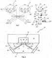
- an analysing system 30 comprising a fluid container 32 or reaction vessel, e.g. a cuvette, defining a sample chamber 34 for containing a sample, e.g. an assay sample, to be analysed.
- the fluid container 32 may comprise a microfluidic flow channel.
- the sample is a liquid or fluid that includes an analyte such as chemical or biological material.
- the sample comprises a plurality of nanoentities 50.
- the sensor 10 is coupled to the fluid container 32 (via the carrier 18 in this example) such that the obverse face 14 and in particular the nanostructured surface is exposed to the chamber 34, i.e. exposed to and typically immersed in the sample during use.
- the nanoentities 50 are configured to bind to the nanostructures 16 on the nanostructured surface.
- Figure 1B shows a detailed view of the nanostructured surface of the sensor 10 and in particular shows the plurality of nanoentities 50 located adjacent to the nanostructures 16.
- the nanoentities 50 may comprise any suitable shape however, preferably, as is shown in the figures the nanoentities may be spherical in shape.
- the nanoentities 50 are preferably formed from an electrically conductive material, typically a metallic material, for example, any of silver, gold, aluminium, platinum, copper or any noble metal or any combinations of the aforesaid.
- the nanoentities 50 may be 1nm to 100nm in diameter.
- a seal (not shown), such as an 0-ring, is typically provided between the sensor 10 and the fluid container 32 to keep the sample within the chamber 34.
- the reverse face 13 of the sensor 10 is exposed to allow excitation radiation to be directed onto the reverse face 13 of the sensor 10, thereby reaching the nanostructures 16 through the body 12, and to allow radiation reflected from the nanostructures 16 to emerge out of the body 12 through the reverse face 13.
- the analysis apparatus 30 includes an excitation and detection apparatus 35 configured to direct a beam of incident radiation Li, e.g. a beam of light in preferred embodiments, from an excitation source 36 to the sensor 10, and in particular to the reverse face 13 of the body 12, and to direct a beam of reflected radiation Lr, e.g. a beam of reflected light in preferred embodiments, from the sensor 10, and in particular radiation emerging from the sensor 10 through the reverse face 13 to a detector 40.
- a beam of incident radiation Li e.g. a beam of light in preferred embodiments
- Lr e.g. a beam of reflected light in preferred embodiments
- the container 32 is received in a cuvette block 33 which can be releasably secured to the excitation and detection apparatus 35, for example by one or more clamps (not shown).
- the carrier 18 may be fixed to the block 33 by any convenient means, e.g. adhesive, or under the action of the clamps.
- the sensor 10 is positioned between the block 33 and the excitation and detection apparatus 35.
- the excitation source 36 generates a beam of electromagnetic radiation.
- the 40 excitation source 36 is of a type that generates light, especially visible light but more generally light having a wavelength typically between approximately 300 nm to 1500 nm.
- the preferred excitation source 36 is of a type that generates polarised radiation, preferably p-polarised light, also known as transverse-magnetic light.
- P-polarized light is linearly polarized light with polarization direction lying in the plane of incidence.
- the plane of incidence is the plane which contains the surface normal and the propagation vector of the incoming light radiation.
- Polarized light with its electric field along the plane of incidence is thus denoted p-polarized.
- P polarized radiation is commonly referred to as transverse-magnetic (TM) radiation.
- TM transverse-magnetic
- TM transverse-magnetic
- TM transverse-magnetic
- TM transverse-magnetic
- TM transverse-magnetic
- a stand LED light source with a polarising filter may be used as the light source 36.
- the respective nanostructures 16 of the regions 5, 6 of the sensor 10 may be configured to resonate when illuminated by radiation as respective different wavelengths.
- each region 5, 6 may be configured to resonate at a respective wavelength that corresponds to a respective wavelength of the radiation produced by the excitation source 36.
- the excitation source 36 is operable to produce radiation at more than one wavelength, preferably the nanostructured surface of the sensor 10 comprises at least one nanostructured region 5, 6 for each of the wavelengths at which the respective nanostructures are configured to resonate when illuminate by the radiation of the excitation source 36 at the respective wavelengths.
- the detector 40 detects electromagnetic radiation that is reflected from the sensor 10.
- the detector 40 is of a type that is compatible with the excitation source 36 and so, in typical embodiments, comprises a light detector. e.g. a photodetector such as the Thorlabs PDA 100 (RTM).
- the excitation and detection apparatus 35 includes a light guide 42 configured to direct the incident and reflected beams Li, Lr to and from the sensor 10.
- the preferred light guide 42 includes an excitation channel 44 for directing the incident radiation to the sensor 10.
- the channel 44 which is typically linear, extends from the excitation source 36 to the exposed reverse face 13 of the body 12.
- the light guide 42 preferably includes a detection channel 46 for directing the reflected radiation to the detector 40.
- the detection channel 46 which is typically linear, extends from the exposed reverse face 13 of the body 12 to the detector 40.
- the channels 44, 46 contact the reverse face 13 at a respective separate part of the reverse face 13.
- the excitation and detection apparatus may for example comprise the excitation source, the detector and means for focussing and/or collimating one or both of the radiation beams, e.g. one or more lenses, and/or the excitation source may be of a type that generates a focussed beam, e.g. a laser.
- the excitation and detection apparatus may comprise a hollow block on which the excitation source and detector are mounted and positioned to direct light to and receive light from the sensor through the hollow interior of the block.
- one or more focussing and/or collimating lenses may be provided at the excitation source and/or at the detector.
- a non-reflective coating may be applied to the interior of the block.
- the light guide 42 has a solid body 48 in which the channels 44, 46 are formed by any conventional means, e.g. drilling or moulding.
- the body 48 need not be solid.
- it may comprise a frame holding one or more tubes which define the, or each channel 44, 46.
- the walls forming the channels 44, 46 are typically opaque to the radiation although this is not essential depending on how the radiation is carried through the channels 44, 46.
- the radiation may propagate directly through the, or each, channel 44, 46 in which case the channel walls should be opaque.
- the radiation may propagate through a light guide, e.g. a fibre optic cable, which is located in the respective channel 44, 46, in which case the channel walls need not be opaque.
- a non-reflective coating may be applied to the interior surface of the channels.
- the excitation and detection apparatus 35 is configured so that the excitation radiation Li is incident on the reverse face 13 of the body 12 at an angle e1, measured with respect to the surface normal, that is equal to or substantially equal to the Brewster angle (also known as Brewster's angle or the polarisation angle).
- the Brewster angle is the angle of incidence at which light with a particular polarization, in this case p-polarisation, is perfectly transmitted through the surface, in this case the reverse face 13 of the body 12, of a transparent medium when passing from a first medium to a second medium which have different refractive indices, with no reflection from the surface.
- the first medium is that of the channel 44 and is typically air
- the second medium is that of the body 12, which is typically glass.
- the Brewster angle for an air/glass interface is approximately 57° (where the glass has a refractive index of 1.52). It will be understood that the Brewster angle may be different for different media that may be used in alternative embodiments of the invention, including glass having a different refractive index than 1.52.
- the channel 44 is angled with respect to the reverse face 13 such that the radiation beam Li is incident on the reverse face 13 at or substantially at the Brewster angle, thereby eliminating or substantially eliminating reflections from the reverse face 13.
- the radiation may be directed by other means as indicated above, but still passes through a medium, typically air, as it travels from the excitation source to the reverse face of the sensor, and from the sensor to the detector.
- the medium is contained within the excitation and detection apparatus 35, e.g. in one or more chambers through which the radiation travels.
- the excitation beam Li hits the reverse face 13, it is refracted by the body 12.
- the angle of incidence e2 of the excitation beam Li at the obverse face 14 of the body 12 is less than the angle of incidence el of the beam Li at the reverse face 13 (with respect to the normal) of the substrate 18.
- the arrangement is such that e2 is less than the angle required to achieve attenuated total reflection (ATR) within the body 12.
- the body 12 is made of a material (e.g. glass) having a higher refractive index than the medium (e.g. air) through which the light is propagated to reach the body 12.
- plasmonic oscillations which may also be referred to as plasmonic resonance, are caused in the nanostructured surface 14 of the sensor 10 in response to radiation beam Li incident at the reverse of the nanostructured face 14 of the sensor, advantageously at an angle of incidence below that required for ATR.
- Plasmonic oscillations occur in the nanostructured surface in a direction that is normal to the obverse face 14. More generally, the plasmonic oscillations occur in directions that are possible to be excited by the radiation.
- plasmonic oscillations occur both along and transverse to the longitudinal axis of the nanostructures 16. The plasmonic oscillations along the longitudinal axis resonances are in this case used for sensing, which requires a component of the excitation light to be at non-normal incidence on the reverse face 13.
- ATR is not possible at face 14 because face 13 is parallel to it.
- a prism (not shown) would have to be used instead of the preferred slide.
- plasmons can be excited in the nanostructured surface 14 with the excitation incident at any angle without getting to an ATR angle.
- the only incidence angle that gives low reflection from parallel face 13 is the Brewster angle.
- the incident radiation impinges on the face 13 at the Brewster angle to eliminate or substantially eliminate reflections from the face 13.
- the incident radiation Li subsequently impinges on the reverse of the nanostructured surface 14, and is reflected by the reverse face of the nanostructured surface 14 whereupon it travels back through the body 12, emerging from the reverse face 13 and being directed to the detector 40 as the reflected radiation beam Lr.
- the reflected beam Lr is directed from the body 12 to the detector 40 by the channel 46 (either directly by the channel 46 or by a light guide (not shown) located in the channel 46).
- the plasmonic oscillations in the nanostructured surface 14 of the sensor 10 interact with the sample in the chamber 34 and, depending on what is contained in the sample, these interactions affect one or more characteristics of the reflected beam Lr, for example its intensity.
- changes in the intensity e.g. a modulation of intensity
- the detector 40 can determine one or more characteristics of the sample, e.g. relating to its composition. Any suitable conventional analysis may be used for this purpose.
- the detector 40 may comprise a photodiode or CCD camera.
- plasmonic oscillations in the sensor 10 are caused by an excitation beam Li incident on the reverse face nanostructured surface 14.
- the Brewster angle is not used to get minimum reflectivity at the reverse face nanostructure surface 14; instead preferred embodiments use the Brewster angle for p-polarised radiation to minimise unwanted reflection from the reverse face 13 of the body 12.
- the nanostructured surface 14 of the sensor 10 can generate plasmonic oscillations when excited at an angle less than required for ATR. This makes the apparatus 30 simpler and cheaper in comparison with known alternatives that use ATR prisms to create ATR of the light to excite surface plasmons in a gold or silver planar film.
- the sample which is typically contained within a reaction vessel such as the sample chamber 34, preferably comprises the plurality of nanoentities 50.
- the nanoentities 50 are configured to bind with both the analytes 55 and/or the nanostructures 16 such that the analytes 55 may be immobilised upon the nanostructured surface when the nanoentities 50 are simultaneously bound to both the analytes 55 and the nanostructures 16.
- the nanoentities 50 are configured to bind to both the nanostructures 16 and the analytes 55 by respective binding couples, wherein each binding couple comprises a first member which has a binding affinity for a second member and vice versa.
- the first and second members of the binding couples ideally comprise complimentary receptors and ligands such as an antibody and a corresponding antigen such that the binding couple when bound forms an antibody-antigen conjugation.
- the nanostructures 16 of the nanostructured surface may be functionalised i.e. by coating other any other suitable means including standard biological protocol, with a first member of a binding couple which is operable to bind with a second member of the binding couple located upon the nanoentities 50.
- the nanoentities 50 may be functionalised i.e. by coating or any other suitable means, with at least an antibody which is co-operable with the antigen of a specific analyte.
- the binding of the nanoentities 50 to the nanostructured surface disrupts the plasmonic resonance excited upon the nanostructured surface resulting in a detectable change in optical reflection of the reflected beam Lr which may be measured by the detector 40 to indicate the presence and/or concentration of one or more analytes 55.
- At least part of the nanostructured surface is coated with a first member 51 of a primary binding couple 59 (as shown in figure 2 ) having an affinity for a second member 52 of the primary binding couple 59 which is coated upon at least some of the nanoentities 50 (see Figure 2A ). Consequently the nanoentities 50 are therefore operable to bind to the nanostructured surface by the binding of the primary binding couple 59.
- the nanoentities 50 may be further coated with a first member 53 of a secondary binding couple 60 having an affinity for a second member 54 of the secondary binding couple 60 which comprises at least one of the analytes 55 contained within the sample.
- the primary and secondary binding couples 59, 60 the analytes 55 contained within the sample may be immobilised upon the nanostructured surface.
- the primary and secondary binding couples 59, 60 ideally comprise complimentary receptor and ligands.
- the nanostructures 16 are coated in the first member 51 of the primary binding couple 59 which comprises a receptor such as an antibody.
- the nanoentity 50 shown coated in the second member 52 of the primary binding couple 59 which in this case comprises a ligand such as an antigen, which is complementary to the receptor located on the nanostructures 16.
- the first and second members 51, 52 of the primary binding couple 59 may be reversed such that the ligand is located upon the nanostructures 16 and the receptors are located upon the nanoentities 50.
- the nanoentity 50 is additionally coated in the first member 53 of the secondary binding couple 60 which in this case comprises a receptor such as an antibody, which is complimentary to the second member 54 of the secondary binding couple 60.
- a first variation of analyte 55 shown in figure 2B , comprises the second member 54 of the secondary binding couple 60 which typically comprises a ligand, in this case an antigen, which is operable to bind to the receptor, comprising an antibody, located upon the nanoentity 50, as is shown in Figure 2C , to form a nanoentity - analyte complex through conjugation.
- the nanoentity 50 is bound to both the analyte 55, the nanostructures 16 by the primary and secondary binding couples 59, 60, the analyte 55 is immobilised on the nanostructured surface as is shown in Figure 2D .
- the second region 6 of the nanostructured surface of the sensor 10 may be coated in a first member 65 of a tertiary binding couple 70 (shown in figure 3 ) which is operable to bind with a second member 66 of the tertiary binding couple 70 which may be coated upon some of the nanoentities 50' contained within the sample. Further these same nanoentities 50' may be coated in a first member 67 of a quaternary binding couple 71 which has a binding affinity for a second member 68 of the quaternary binding couple 71 which is located upon a second variation of analyte 55'.
- the first member 65 of the tertiary binding couple 70 preferably comprises a receptor, in particular an antibody whilst the second member 66 ideally comprises a complimentary ligand, in particular an antigen.
- the first member 67 of the quaternary binding couple 71 typically comprises a receptor, in particular an antibody whilst the second member 68 of the quaternary binding couple 71 preferably comprises a complimentary ligand, in particular an antigen.
- nanostructured surface may be coated in additional binding members (not shown) such that further variations of analytes 55, 55' contained within the sample may be immobilised upon the nanostructured surface of the sensor 10 in the manner recited above.
- one or more regions of the nanostructured surface may be functionalised, typically by coating with at least one binding member which is complimentary to a binding member of one or more of the analytes 55, 55' contained within the sample such that the analyte(s) 55, 55' may be directly immobilised upon the nanostructured surface.
- the nanostructured surface may be coated with an antibody which is complimentary with an antigen of a pathogen contained within the sample, such that the pathogen may be immobilised on the nanostructured surface.
- the binding between the nanoentities 50, 50' and the nanostructures 16, such as the primary and tertiary binding couples 59, 70, may be affected by a peptide binder or aptamer that has an affinity for the antigen located on the analyte 55.
- the binding between the first and second members of the secondary binding couple 60 and the first and second members of the tertiary binding couple 70 may be affected by a mixture of antibody/peptide binders and/or aptamers which are operable to interact with a range of antigens on the analytes 55, 55'.
- the binding between, the nanoentities 50, 50' and the analytes 55, 55', in particular the binding of the secondary and quaternary binding couples 60, 71, may be affected by a peptide binder or aptamer that has an affinity for the antigen located on the analyte 55.
- the binding between the first and second members 53, 54 of secondary binding couple 60, or first and second members of the quaternary binding couples may be affected by a mixture of antibody/peptide binders and/or aptamers which are operable to interact with a range of antigens on the analyte 55.
- the analyte 55, 55' typically comprises biological material, for example the analyte may comprise a pathogen such as a virus, bacterium or fungus. Alternatively the analyte may comprise a biological element which is secreted or otherwise produced from a cell for example outer membrane vesicles secreted by Gram negative bacteria. Further the analytes 55 may comprise extracellular secreted proteins, human biomarkers, immunoglobulin or human cells.
- the quantity of nanoentities 50, 50' which are mixed with the sample is known prior to their introduction into the sample. Additionally or alternatively, prior to the sample being introduced into the sample chamber 34, the sample may undergo separation such that only the particular analytes 55, 55' of which it is desired to measure the concentration of, are introduced into the sample chamber 34 with other elements of the sample being removed. In such an embodiment the sample may be mixed with a plurality of nanoentities 50, 50' which are configured to bind with the particular analytes 55, 55'.
- the sample may then undergo separation to remove the binding couples from the unbound nanoentities 50, 50' and analytes 55, 55'.
- the binding couples of the nanoentities 50, 50' and the analyte 55, 55' may be separated from the sample by mass or size using a centrifuge or a filter respectively.
- the use of a filter to separate the binding couples from the sample is illustrated in Figure 5 . Subsequently this solution of binding couples may then be introduced into the sample chamber 34 for analysis.
- the analysis may include obtaining measurements of the reflection characteristics of the nanostructured surface when the nanoentity-analyte binding couples are immobilised, by binding, upon the nanostructured surface, these measurements may then be compared with measurements obtained when a known quantity of nanoentities 50, 50' are bound to the nanostructured surface.
- the known quantity may comprise at least one nanoentity 50, 50' bound to the nanostructured surface or more preferably the known quantity may comprise the total quantity of nanoentities 50, 50' which were introduced to the sample prior to separation.
- the unbound nanoentities 50, 50' may be separated from the sample to leave the binding couples therein.
- the unbound nanoentities 50, 50' may then be re-suspended in a fresh buffer and introduced into the sample chamber 34 such as to interact with the nanostructured surface of the sensor 10 to give a detectable signal.
- the measurements obtained when the unbound nanoentities 50, 50' are immobilised upon, typically by binding, the nanostructured surface are compared to measurements obtained when the known quantity of nanoentities50, 50' are immobilised thereupon such that a ratio can be obtained to determine the concentration of analytes 55, 55' which were bound to the nanoentities 50, 50' in the sample.
- the nanoentities 50, 50' that are bound to the analytes 55, 55' undergo chemical detachment from the nanostructured surface. These are then re-suspended in a buffer and interact with the nanostructured chip surface to give a detectable change in the reflection characteristics of the nanostructured surface.
- the detached analyte 55, 55' may then be separated therefrom to be used for further downstream analysis.
- the biological sample undergoes cell lysis.
- the lytic reaction liberates nucleic acid from cells and virus particles in the biological sample.
- the nucleic acid is separated from the cell debris and re-suspended in fresh buffer along with functionalised nanoentities 50.
- Nanoentities are functionalised with single stranded nucleic acid sequences. These sequences are complementary to sequences of interest in the nucleic acid sample.
- the sample/nanoentity mixture is incubated to promote formation of nanoentity/nucleic acid complexes through binding of probes to complementary sequences in sample.
- the nanoentity/nucleic acid complex is then separated from the biological sample and unbound nanoentities.
- the detection on the nanostructure chip surface will be through a mixture of nanoentity 50, 50' - analyte 55, 55' binding couples and analyte only bindings with the nanostructured chip surface.
- a further aspect of the invention provides a biochip 101 comprising the analysing system 30 which may be incorporated within a microfluidic chip which is generally indicated by the reference numeral 100 as shown in figure 6 .
- the reaction vessel may comprise a microfluidic flow channel.
- the microfluidic chip 100 typically comprises an initial sample receiving chamber 103 which is operable to receive the sample containing the analyte 55, 55'.
- the microfluidic chip 100 additionally comprises one or more injection chambers 104, which may contain the plurality of nanoentities 50 at least some of which may be coated in a particular first binding member which is complimentary to a particular second binding member of at least one of the analytes 55 contained within the initial sample receiving chamber 103. Further one or more of the other nanoentities 50' may be coated in a different first member of a binding couple which is complimentary to a particular second binding member of one or more different analytes 55' contained within the sample.
- the initial sample receiving chamber 103 and injection chamber 104 are fluidically coupled to one another by a mixing chamber 105 where the nanoentities 50, 50' may be mixed with the sample received from the initial sample receiving chamber 103.
- the mixing chamber 105 is further fluidically coupled to a separation chamber 106 which is configured to separate the one or more analytes 55 contained within the sample, as for example the analytes 55 may comprise different types of biological material as described previously, for example the analytes 55 may comprise bacteria, proteins, cells and/or viruses.
- the separation chamber 106 may comprise a centrifuge or a filter such that the analytes 55 may be separated from the sample by mass or size respectively.
- a series of filters with decreasing pore size may be used to separate out the analytes 55 of interest from the biological sample.
- the plurality of analytes 55 can be separated from the sample mixed with the nanoentities received from the mixing chamber, wherein the separation chamber 105 may be fluidically coupled to the biochip 101 by one or more microfluidic flow channels 107.
- the microfluidic flow channels fluidically couple the separation chamber 105 to the sample chamber of the analysing system 30.
- the number of microfluidic flow channels 107 may correspond to the number of analytes 55, 55' to be separated from the sample or vice versa, wherein a channel 107 may be provided for each specific analyte 55, 55'.
- different regions 5, 6 of the sensor 10 may be configured to bind with particular analytes 55 contained within the sample.
- different regions 5, 6 may be coated in different first binding members complimentary to different second binding members of the nanoentities 50, 50' which are in turn further coated in different binding members which are complimentary to that of the different analytes such that each region 5 of the nanostructured surface may be complimentary to a specific analyte separated from the sample.
- the nanostructures 16 of the first region 5 may be coated in antibodies that are complementary to the antigen on the surface of the nanoentities 50, which is further coated in an antibody which is complimentary with the antigen of a specific analyte 55.
- the sample may only contain one nanoentity and accordingly no separation chamber 106 may be required upon the microfluidic chip 100, in this embodiment the mixing chamber 105 may be coupled directly to the biochip 101.
- the microfluidic chip 100 may further comprise a suction chamber 108 which is fluidically coupled to the biochip 101, in particular to the sample chamber of the biochip 101.
- the suction chamber 108 may be fluidically coupled to a waste chamber and/or outlet 109.
Abstract
Description
- This invention relates to an analysing system for the detection of an analyte and in particular to an analysing system for the detection of a biomarker or pathogen.
- Rapid detection of clinically relevant biomarkers and pathogens from biological samples is a critical step in the diagnosis of disease. This is true not only in health care diagnostics but in veterinary science, agri-food production and food safety. Traditional methods require several sequential steps from initial sample collection through to detection of the pathogen of interest. These steps can often require complex pre-analysis processing, enrichment or amplification steps in order to ensure adequate sensitivity to make the test fit for purpose followed by complex data interpretation. Multiple sample treatment steps can lead to a loss of sensitivity for the downstream detection method or introduces potential points of contamination thus bringing into question the validity of results. Furthermore, some automated techniques lack the relevant diagnostic sensitivity meaning that traditional microbiology techniques like total viable counts are still employed as the method of choice. This is a time consuming process often taking days to get a definitive result.
- Within healthcare setting, three main workflows are used in the diagnostic algorithm. The first is culture based methods; they rely on an enrichment step and are generally used for bacterial pathogens. These tests are limited by how quickly the organisms in the sample grow in the enrichment media and are highly susceptible to contamination. The second method is molecular tests. Molecular biology requires a high level of operational expertise, significant infrastructure to limit cross contamination and expensive system and consumables to run the tests. These tests are much more expensive than culture based methods but offer a much higher level of sensitivity. The typical turnaround time for batch processing PCR is anywhere between 12-24hrs. The third method is immunoassay based tests. These rely on the principal behind antibody - antigen reactions. Antibody-antigen reactions offer a highly specific mechanism for the detection of pathogens of interest. All immunoassay tests are based around this biological principal. The test relies upon the specificity of an antibody to an antigen on a particular pathogen of interest in a biological sample. This antibody (referred to as the primary antibody) binds to the pathogen via the specific antigen thus capturing the pathogen of interest in the biological sample. A second reaction is then carried out whereby a labelled antibody (referred to as the secondary antibody) binds specifically to the primary antibody. The secondary antibody is labelled with some form of reporter molecule. This molecule gives off a detectable signal. This signal can be light or colour change of a substrate that can be measured by a detector system. Due to the multiple steps required to complete an immunoassay test, it can be time consuming or require expensive liquid handling system to screen samples for a range of biomarkers or pathogens furthermore, sensitivity is not comparable with PCR based methods.
- More recently there has been a growing trend towards label free detection of biomarkers/pathogens of interest. Localised surface plasmon resonance (LSPR) is generated by nanoparticles or structures. These are typically gold or silver. LSPR produces a strong resonance absorbance peak in the visible light range of the spectrum. This absorbance peak is highly sensitive to refractive index changes close to the surface of the nanoparticle. One limitation in LSPR biosensors is the ability to detect minute quantities of small molecules. Since the detection relies on a refractive index change at the surface of the nanoparticle, a relatively high concentration of small molecules is required to induce this.
- It is a desire of the present invention to overcome the above mentioned limitations with LSPR biosensors.
- A first aspect of the present invention provides an analysing system comprising: a fluid container defining a sample chamber, wherein a sample is contained in the sample chamber; a sensor comprising a transparent body with a reverse face and an obverse face, the obverse face having a nanostructured surface, the nanostructured surface comprising a plurality of elongate nanostructures having a respective longitudinal axis that is disposed substantially perpendicularly to the obverse face; an excitation and detection apparatus comprising an excitation source for generating a beam of polarised radiation and a corresponding radiation detector, wherein, the sensor is coupled to the fluid container such that the nanostructured surface is exposed to the sample chamber, to the sample located therein; and wherein the excitation and detection apparatus is configured to direct a beam of incident polarised electromagnetic radiation onto the reverse face of the body at an angle that causes no or substantially no reflection of the polarised radiation from the reverse face, and wherein said excitation and detection apparatus is configured to direct to said detector a beam of reflected radiation, said beam of reflected radiation comprising said incident radiation emerging in use from the reverse face after reflection from said nanostructured surface; wherein the sample comprises a plurality of nanoentities and one or more analytes and wherein the nanoentities are operable to bind with the nanostructures and the one or more analytes.
- Ideally, when the nanoentities are bound to both the nanostructures and the analyte simultaneously, the analyte being immobilised upon the nanostructured surface.
- Preferably, the nanostructured surface comprises a plurality of spaced apart regions.
- Ideally, at least a first region of the nanostructured surface is functionalised with a first member of a primary binding couple having an affinity for a second member of the primary binding couple which is functionalised upon at least some of the nanoentities.
- Preferably, the nanoentities are further functionalised with a first member of a secondary binding couple having an affinity for a second member of the secondary binding couple which comprises at least one of the analytes contained within the sample.
- Ideally, the analyte is functionalised with the second member of the secondary binding coupe.
- Preferably, at least a second region of the nanostructures is functionalised with a first member of a tertiary binding couple having an affinity for a second member of the tertiary binding couple which is coated upon some of the nanoentities.
- Ideally, the nanoentities which are functionalised with the second member of the tertiary binding couple are further functionalised with a first member of a quaternary binding couple which has an affinity for a second member of the quaternary binding couple which comprises at least one of the analytes contained within the sample.
- Preferably, the analyte is functionalised with the second member of the quaternary binding couple.
- Ideally, the binding couples comprise receptor-ligand binding couples.
- Preferably, the first member of the primary and/or tertiary binding couples comprises an antibody and the second member of the primary binding couple comprises a complimentary antigen.
- Ideally, the first member of the secondary and/or quaternary binding couple comprises an antibody and the second member comprises a complimentary antigen.
- Preferably, the analyte comprises a pathogen.
- Ideally, the pathogen comprises a virus, bacterium or fungus.
- Preferably, the analyte comprises extracellular secreted proteins, human biomarkers, immunoglobulin or human cells.
- Ideally, the nanoentities are formed from an electrically conductive material, typically a metallic material for example gold, aluminium, copper or any noble metal or any combinations of the aforesaid.
- Preferably, the nanoentities are spherical in shape.
- Ideally, the nanostructures and/or nanoentities and/or analyte are functionalised by being coated with the respective binding member or members.
- Ideally, each of the plurality of regions are connected to a respective electrical terminal.
- Preferably, respective different electrical bias may be applied to each of the regions by respective power supplies coupled to the electrical terminals.
- Ideally, the respective nanostructures of each region are configured to resonate when illuminated by radiation at respective different wavelengths.
- Preferably, the respective nanostructures of each region are configured to resonate at a respective wavelength that corresponds to a respective wavelength of the radiation produced by said excitation source.
- Ideally, the excitation source is operable to produce radiation at more than one wavelength, and wherein said nanostructured surface includes at least one of said nanostructured region for each of said wavelengths in which the respective nanostructures are configured to resonate when illuminated by the radiation at the respective wavelength.
- A second aspect of the invention provides a microfluidic chip comprising the analysing system of the first aspect of the invention.
- Preferably, the analysing system of the first aspect of the invention is provided in a biochip which is coupled to or mounted upon the microfluidic chip.
- Ideally, the microfluidic chip, further comprising an initial sample receiving chamber which is operable to receive the sample containing the one or more analyte.
- Preferably the microfluidic chip, further comprising an injection chamber which contains the plurality of nanoentities, which is operable to inject the nanoentities into the sample.
- Ideally, wherein the sample receiving chamber and injection are fluidly coupled to a mixing chamber, wherein the sample is mixed with the nanoentities.
- Preferably, the mixing chamber is coupled to a separation chamber which is configured to separate the one or more analytes contained within the sample.
- Ideally, the separation chamber comprises a centrifuge or filter.
- Preferably, the separation chamber is fluidically coupled to the biochip by one or more microfluidic flow channels.
- Ideally, different regions of the sensor are configured to bind with particular analytes contained within the sample.
- A third aspect of the invention provides a method of analysing a sample using a sensor comprising the analysing system embodying the first aspect of the invention, the method comprising: Exposing the nanostructured surface to the sample comprising a plurality of nanoentities and/or one or more analytes; Causing the nanoentities to bind with the nanostructures and the one or more analytes; Directing a beam of incident polarised electromagnetic radiation onto the reverse face of the body at an angle that causes no or substantially no reflection of the polarised radiation from the reverse face; and directing to a detector a beam of reflected radiation, said beam of reflected radiation comprising said incident radiation that emerges from the reverse face after reflection from said nanostructured surface.
- Ideally, prior to exposing the nanostructured surface to the sample comprising a plurality of nanoentities and the analyte:
- mixing a known quantity of nanoentities with an analyte, wherein the nanoentities are configured to bind to said analyte to form a plurality of binding couples;
- Separating the binding couples from unbound nanoentities and analytes to define the sample, the sample containing only the binding couples of nanoentities and analytes.
- Preferably, obtaining measurements of the reflection characteristics on the nanostructured surface with the binding couples immobilised thereon.
- Ideally, comparing the measurements of the reflection characteristics of the nanostructured surface with the binding couples immobilised thereon with measurements of the reflection characteristics of the nanostructured surface when a known quantity of nanoentities only are immobilised upon the nanostructured surface to determine the concentration of analyte immobilised upon the nanostructured surface.
- Preferably the known quantity of nanoentities comprises a singular nanoentity or the total quantity of nanoentities which were mixed with the analyte prior to introduction into the analysing system.
- Alternatively, the unbound nanoentities may be separated from the binding couples to define the sample.
- An embodiment of the invention is now described by way of example with reference to the accompanying drawings in which like numerals are used to denote like parts and in which:
-
Figure 1 is a perspective view of a nanostructured plasmonic sensor for use in an analysing system embodying the invention; -
Figure 1A is a detail view of the nanostructured surface of the plasmonic sensor ofFigure 1 ; -
Figure 1B is a detail of the nanostructured surface ofFigure 1 in particular showing a plurality of nanoentities adjacent thereto; -
Figure 2 is a schematic view of an analysing system embodying one aspect of the invention, the apparatus including the plasmonic sensor ofFigure 1 whereby a region of the nanostructured surface is coated in a first member of a first binding couple; -
Figure 2A is a schematic view of a nanoentity, in this case a nanosphere, which is coated in a second member of the first binding couple and a first member of a second binding couple; -
Figure 2B is a schematic view of an analyte, in this case a pathogen, which comprises the second member of the second binding couple; -
Figure 2C is a schematic view showing the binding of the analyte and nanoentity, in particular showing a nanoentity and analyte complex formed by the binding of the first and second members of the second binding couple. -
Figure 2D is a schematic view of the nanostructured surface of the plasmonic sensor offigure 1 showing the analyte immobilised on the nanostructured surface by the binding of analyte to the nanoentity via the second binding couple and the binding of the nanoentity to the nanostructured surface by the first binding couple; -
Figure 3 is a schematic diagram of an alternative embodiment of the invention showing an excitation apparatus directing a beam of polarised radiation at the plasmonic sensor and a corresponding detection apparatus, in particular showing first and second regions of the nanostructured surface with each region being coated in a different first member of a respective binding couple. -
Figure 3A is a schematic diagram of two nanoentities with the nanoentities being coated in respective first and second members of first and second binding couples such that the nanoentities are operable to immobilise different analytes upon the first and second regions of the nanostructured surface as shown infigure 3 ; -
Figure 3B is a schematic diagram showing two different analytes with each analyte comprising different binding members for binding to the differently functionalised nanoentities offigure 3A ; -
Figure 3C is a schematic diagram showing the binding of the different analytes to the two nanoentities by the interaction of the different binding members of the binding couples; -
Figure 4 is a schematic view of an analysing system embodying one aspect of the invention, the system including the plasmonic sensor offigure 1 and in particular showing a fluid container a defining a sample chamber for containing a sample to be analysed; -
Figure 5 is a diagram showing the separation of a high level biological sample comprising multiple analytes by mass or size into discrete pathogen lines e.g. bacteria, proteins, cells and viruses; -
Figure 6 is a schematic diagram showing a microfluidic chip including a biochip comprising the analysing system offigure 4 . - Referring now to
Figure 1 of the drawings there is shown, generally indicated as 10, a nanostructured plasmonic sensor. Thesensor 10 comprises abody 12 with areverse face 13 and anobverse face 14, theobverse face 14 having a nanostructured surface. A nanostructured surface is a surface on which there is formed a plurality of nanostructures. A nanostructure is a structure that has at least one dimension on the nanoscale. For the purposes of the present invention, nanoscale means between 0.1 nm and 1000 nm, more typically between 1 nm and 200 nm. A nanostructure may have only one dimension on the nanoscale, or two dimensions on the nanoscale, or three dimensions on the nanoscale. Nanostructures having three dimensions on the nanoscale are referred to as nanoparticles. -
Figure 1A shows a more detailed view of the nanostructured surface of theobverse face 14. The nanostructured surface comprises a plurality ofnanostructures 16 that are elongate, having a respective longitudinal axis that is disposed substantially perpendicularly to theobverse face 14. Thenanostructures 16 are therefore substantially parallel with each other. In preferred embodiments, thenanostructures 16 are spaced apart from one another, e.g. eachnanostructure 16 is spaced apart from the, or each,adjacent nanostructure 16. Alternatively, at least some and optionally all of thenanostructures 16 are contiguous with the, or each,adjacent nanostructure 16. Thenanostructures 16 may be arranged in a one or two dimensional array, preferably being aligned with each other along the, or each, dimension of the array. Advantageously, the aspect ratio of the length L to the width W of eachnanostructure 16 is greater than 1. The third dimension (not illustrated) of thenanostructures 16 may be of any desired size depending on the application, for example it may be similar to the width W or the length L, or may be unlimited, e.g. the nanostructures may form a grating. In preferred embodiments, at least some and preferably all of thenanostructures 16 are nanoparticles, having three dimensions on the nanoscale. - For example, some or all of the
nanostructures 16 may comprise a rod, wire or a tube, in particular a nanorod, nanowire or nanotube, which may take any suitable shape for example substantially cylindrical or substantially conical. Thenanostructures 16 may be solid or hollow. - The
nanostructures 16 are typically formed from an electrically conductive material, typically a metallic material, for example, any of silver, gold, aluminium, platinum, copper or any noble metal or any combinations of the aforesaid. In typical embodiments, the width W of thenanostructures 16 is approximately 2 nm to approximately 500 nm, usually approximately 10 nm to approximately 100 nm, and the length L of thenanostructures 16 is approximately 10 nm to approximately 2000 nm, usually approximately 50 nm to approximately 500 nm. For example, thenanostructures 16 may have a width of approximately 20 nm and a length of approximately 500 nm. It is preferred that thenanostructures 16 are substantially uniform in width and/or height although this need not necessarily be the case. - Typically, the spacing between
adjacent nanostructures 16 is approximately 2 nm to approximately 1500 nm, usually approximately 20 nm to approximately 500 nm. In preferred embodiments, thenanostructures 16 are spaced apart from one another by a distance less than the wavelength of the excitation light used to cause plasmonic oscillations, as is described in further detail below. The nanoparticle to nanoparticle separation may be periodic, at a scale of approximately 20 nm to approximately 1500 nm. The nanoparticle to nanoparticle separation may be quasi-periodic, at a scale of approximately 20 nm to approximately 1500 nm. Typically, thesensor 10 includes in the order of one billionnanoparticles 16. - The
body 12 provides a mechanical support for thenanostructures 16. Thebody 12 may be made of any convenient material, preferably a dielectric material, for example glass, crystal or plastics. Typically, thebody 12 is substantially planar in shape, having spaced apart, oppositely disposed obverse and reverse faces 13, 14 that are preferably parallel with one another. By way of example, thebody 12 may be between approximately 0.3 to approximately 2 mm thick (i.e. between faces 13, 14. Thebody 12 is made from material that is transparent to the electromagnetic radiation (usually light radiation) that is used to illuminate thesensor 10, as is described in more detail below. In the case where the illuminating radiation is light, thebody 12 may for example be formed from glass. - In typical embodiments, the
nanostructures 16 are formed on alayer 17 of electrically conductive material, typically a metallic layer, provided at theobverse face 4 of thebody 12, i.e. as part of a nanostructured metallic layer on thebody 12. Any conventional fabrication technique that is suitable for forming a nanostructured metallic layer may be used for this purpose. For example, the nanostructures may be formed by electrodeposition, optionally in pores formed in a layer of insulating material, e.g. aluminium oxide. Typically, anadhesive layer 19 is provided between the body 20 and themetallic layer 17. Any conventional adhesive layer material may be used, e.g. titanium or tantalum, and is typically formed by physical vapour deposition. In alternative embodiments, thelayers - To facilitate incorporating the
sensor 10 into an analysing apparatus, thesensor 10 may be mounted on acarrier 18 that exposes thereverse face 13 to allow the radiation to impinge upon and emerge from the reverse face as described herein, and exposes the obverse face to the sample chamber. Thecarrier 18 may be formed form any convenient material, e.g. plastics. Thepreferred carrier 18 is illustrated in and comprises a body in which a through-aperture 21 is formed, thesensor 10 being mounted in the aperture 21 such that its faces 13, 14 are exposed. The body may for example comprise a substantially planar body and may be in the order of 1 mm thick. - As can be seen in
figure 1 the nanostructured surface of thesensor 10, typically formed on theobverse face 14 thereof, may comprise a plurality ofdistinct regions regions regions face 14 to further distinguish them with respect to one another or alternatively theregions regions region electrical terminal 7, to which respective electrical power supplies may be connected such that respective different electrical bias may be applied to each of theregions regions electrical terminal 7 such that the same electrical bias is applied to each region. Additionally or alternatively theregions - Referring now to
Figure 4 , there is shown an analysingsystem 30 comprising afluid container 32 or reaction vessel, e.g. a cuvette, defining asample chamber 34 for containing a sample, e.g. an assay sample, to be analysed. In an alternative embodiment thefluid container 32 may comprise a microfluidic flow channel. Typically the sample is a liquid or fluid that includes an analyte such as chemical or biological material. Additionally the sample comprises a plurality ofnanoentities 50. Thesensor 10 is coupled to the fluid container 32 (via thecarrier 18 in this example) such that theobverse face 14 and in particular the nanostructured surface is exposed to thechamber 34, i.e. exposed to and typically immersed in the sample during use. Preferably, there is direct contact between the nanostructured surface of thesensor 10 and the sample, in particular thenanoentities 50, during use. To his end thenanoentities 50 are configured to bind to thenanostructures 16 on the nanostructured surface. -
Figure 1B shows a detailed view of the nanostructured surface of thesensor 10 and in particular shows the plurality ofnanoentities 50 located adjacent to thenanostructures 16. Thenanoentities 50 may comprise any suitable shape however, preferably, as is shown in the figures the nanoentities may be spherical in shape. Thenanoentities 50 are preferably formed from an electrically conductive material, typically a metallic material, for example, any of silver, gold, aluminium, platinum, copper or any noble metal or any combinations of the aforesaid. Thenanoentities 50 may be 1nm to 100nm in diameter. A seal (not shown), such as an 0-ring, is typically provided between thesensor 10 and thefluid container 32 to keep the sample within thechamber 34. Thereverse face 13 of thesensor 10 is exposed to allow excitation radiation to be directed onto thereverse face 13 of thesensor 10, thereby reaching thenanostructures 16 through thebody 12, and to allow radiation reflected from thenanostructures 16 to emerge out of thebody 12 through thereverse face 13. - The
analysis apparatus 30 includes an excitation anddetection apparatus 35 configured to direct a beam of incident radiation Li, e.g. a beam of light in preferred embodiments, from anexcitation source 36 to thesensor 10, and in particular to thereverse face 13 of thebody 12, and to direct a beam of reflected radiation Lr, e.g. a beam of reflected light in preferred embodiments, from thesensor 10, and in particular radiation emerging from thesensor 10 through thereverse face 13 to adetector 40. - Conveniently, the
container 32 is received in acuvette block 33 which can be releasably secured to the excitation anddetection apparatus 35, for example by one or more clamps (not shown). Thecarrier 18 may be fixed to theblock 33 by any convenient means, e.g. adhesive, or under the action of the clamps. In use, thesensor 10 is positioned between theblock 33 and the excitation anddetection apparatus 35. - The
excitation source 36 generates a beam of electromagnetic radiation. In typical embodiments the 40excitation source 36 is of a type that generates light, especially visible light but more generally light having a wavelength typically between approximately 300 nm to 1500 nm. - More particularly, the
preferred excitation source 36 is of a type that generates polarised radiation, preferably p-polarised light, also known as transverse-magnetic light. P-polarized light is linearly polarized light with polarization direction lying in the plane of incidence. The plane of incidence is the plane which contains the surface normal and the propagation vector of the incoming light radiation. Polarized light with its electric field along the plane of incidence is thus denoted p-polarized. P polarized radiation is commonly referred to as transverse-magnetic (TM) radiation. By way of example a stand LED light source with a polarising filter may be used as thelight source 36. Therespective nanostructures 16 of theregions sensor 10 may be configured to resonate when illuminated by radiation as respective different wavelengths. Furthermore the nanostructures of eachregion excitation source 36. To this end theexcitation source 36 is operable to produce radiation at more than one wavelength, preferably the nanostructured surface of thesensor 10 comprises at least onenanostructured region excitation source 36 at the respective wavelengths. - The
detector 40 detects electromagnetic radiation that is reflected from thesensor 10. Thedetector 40 is of a type that is compatible with theexcitation source 36 and so, in typical embodiments, comprises a light detector. e.g. a photodetector such as the Thorlabs PDA 100 (RTM). - In preferred embodiments, the excitation and
detection apparatus 35 includes alight guide 42 configured to direct the incident and reflected beams Li, Lr to and from thesensor 10. The preferredlight guide 42 includes anexcitation channel 44 for directing the incident radiation to thesensor 10. Thechannel 44, which is typically linear, extends from theexcitation source 36 to the exposedreverse face 13 of thebody 12. Thelight guide 42 preferably includes adetection channel 46 for directing the reflected radiation to thedetector 40. Thedetection channel 46, which is typically linear, extends from the exposedreverse face 13 of thebody 12 to thedetector 40. Optionally, thechannels reverse face 13 at a respective separate part of thereverse face 13. - In alternative embodiments, the
light guide 42 andchannels - In the illustrated embodiment, the
light guide 42 has asolid body 48 in which thechannels body 48 need not be solid. For example it may comprise a frame holding one or more tubes which define the, or eachchannel channels channels channel respective channel - In preferred embodiments, the excitation and
detection apparatus 35 is configured so that the excitation radiation Li is incident on thereverse face 13 of thebody 12 at an angle e1, measured with respect to the surface normal, that is equal to or substantially equal to the Brewster angle (also known as Brewster's angle or the polarisation angle). The Brewster angle is the angle of incidence at which light with a particular polarization, in this case p-polarisation, is perfectly transmitted through the surface, in this case thereverse face 13 of thebody 12, of a transparent medium when passing from a first medium to a second medium which have different refractive indices, with no reflection from the surface. In this example, the first medium is that of thechannel 44 and is typically air, while the second medium is that of thebody 12, which is typically glass. The Brewster angle for an air/glass interface is approximately 57° (where the glass has a refractive index of 1.52). It will be understood that the Brewster angle may be different for different media that may be used in alternative embodiments of the invention, including glass having a different refractive index than 1.52. - Hence, in the preferred embodiment, the
channel 44 is angled with respect to thereverse face 13 such that the radiation beam Li is incident on thereverse face 13 at or substantially at the Brewster angle, thereby eliminating or substantially eliminating reflections from thereverse face 13. In embodiments where the light guide is omitted, the radiation may be directed by other means as indicated above, but still passes through a medium, typically air, as it travels from the excitation source to the reverse face of the sensor, and from the sensor to the detector. In such cases, the medium is contained within the excitation anddetection apparatus 35, e.g. in one or more chambers through which the radiation travels. - In use, when the excitation beam Li hits the
reverse face 13, it is refracted by thebody 12. Hence, the angle of incidence e2 of the excitation beam Li at theobverse face 14 of the body 12 (with respect to the normal of those surfaces) is less than the angle of incidence el of the beam Li at the reverse face 13 (with respect to the normal) of thesubstrate 18. Advantageously, the arrangement is such that e2 is less than the angle required to achieve attenuated total reflection (ATR) within thebody 12. Typically, thebody 12 is made of a material (e.g. glass) having a higher refractive index than the medium (e.g. air) through which the light is propagated to reach thebody 12. - In use, plasmonic oscillations, which may also be referred to as plasmonic resonance, are caused in the
nanostructured surface 14 of thesensor 10 in response to radiation beam Li incident at the reverse of thenanostructured face 14 of the sensor, advantageously at an angle of incidence below that required for ATR. Plasmonic oscillations occur in the nanostructured surface in a direction that is normal to theobverse face 14. More generally, the plasmonic oscillations occur in directions that are possible to be excited by the radiation. In the preferred embodiments where thenanostructures 16 are elongate, plasmonic oscillations occur both along and transverse to the longitudinal axis of thenanostructures 16. The plasmonic oscillations along the longitudinal axis resonances are in this case used for sensing, which requires a component of the excitation light to be at non-normal incidence on thereverse face 13. - In preferred embodiments, ATR is not possible at
face 14 becauseface 13 is parallel to it. For ATR to occur, a prism (not shown) would have to be used instead of the preferred slide. Accordingly, in preferred embodiments, plasmons can be excited in thenanostructured surface 14 with the excitation incident at any angle without getting to an ATR angle. The only incidence angle that gives low reflection fromparallel face 13 is the Brewster angle. - Advantageously the incident radiation impinges on the
face 13 at the Brewster angle to eliminate or substantially eliminate reflections from theface 13. The incident radiation Li subsequently impinges on the reverse of thenanostructured surface 14, and is reflected by the reverse face of thenanostructured surface 14 whereupon it travels back through thebody 12, emerging from thereverse face 13 and being directed to thedetector 40 as the reflected radiation beam Lr. Advantageously, there is no ATR of the beams Li, Lr within thebody 12. In preferred embodiments, the reflected beam Lr is directed from thebody 12 to thedetector 40 by the channel 46 (either directly by thechannel 46 or by a light guide (not shown) located in the channel 46). - The plasmonic oscillations in the
nanostructured surface 14 of thesensor 10 interact with the sample in thechamber 34 and, depending on what is contained in the sample, these interactions affect one or more characteristics of the reflected beam Lr, for example its intensity. For example, changes in the intensity (e.g. a modulation of intensity) can be caused by an alteration of the resonance conditions of thenanostructures 16. Hence, by analysing one or more characteristics of the reflected beam Lr, thedetector 40 can determine one or more characteristics of the sample, e.g. relating to its composition. Any suitable conventional analysis may be used for this purpose. Thedetector 40 may comprise a photodiode or CCD camera. - It will be seen that in preferred embodiments, plasmonic oscillations in the
sensor 10 are caused by an excitation beam Li incident on the reverse facenanostructured surface 14. The Brewster angle is not used to get minimum reflectivity at the reverseface nanostructure surface 14; instead preferred embodiments use the Brewster angle for p-polarised radiation to minimise unwanted reflection from thereverse face 13 of thebody 12. This is possible because thenanostructured surface 14 of thesensor 10 can generate plasmonic oscillations when excited at an angle less than required for ATR. This makes theapparatus 30 simpler and cheaper in comparison with known alternatives that use ATR prisms to create ATR of the light to excite surface plasmons in a gold or silver planar film. - To enhance the detection of one or
more analytes 55 contained with the sample, the sample which is typically contained within a reaction vessel such as thesample chamber 34, preferably comprises the plurality ofnanoentities 50. Thenanoentities 50 are configured to bind with both theanalytes 55 and/or thenanostructures 16 such that theanalytes 55 may be immobilised upon the nanostructured surface when thenanoentities 50 are simultaneously bound to both theanalytes 55 and thenanostructures 16. Thenanoentities 50 are configured to bind to both thenanostructures 16 and theanalytes 55 by respective binding couples, wherein each binding couple comprises a first member which has a binding affinity for a second member and vice versa. The first and second members of the binding couples ideally comprise complimentary receptors and ligands such as an antibody and a corresponding antigen such that the binding couple when bound forms an antibody-antigen conjugation. Thenanostructures 16 of the nanostructured surface may be functionalised i.e. by coating other any other suitable means including standard biological protocol, with a first member of a binding couple which is operable to bind with a second member of the binding couple located upon thenanoentities 50. Typically thenanoentities 50 may be functionalised i.e. by coating or any other suitable means, with at least an antibody which is co-operable with the antigen of a specific analyte. Advantageously the binding of thenanoentities 50 to the nanostructured surface disrupts the plasmonic resonance excited upon the nanostructured surface resulting in a detectable change in optical reflection of the reflected beam Lr which may be measured by thedetector 40 to indicate the presence and/or concentration of one or more analytes 55. - To this end at least part of the nanostructured surface, typically at least the
first region 5 of the nanostructured surface of thesensor 10, is coated with afirst member 51 of a primary binding couple 59 (as shown infigure 2 ) having an affinity for asecond member 52 of the primarybinding couple 59 which is coated upon at least some of the nanoentities 50 (seeFigure 2A ). Consequently thenanoentities 50 are therefore operable to bind to the nanostructured surface by the binding of the primarybinding couple 59. Thenanoentities 50 may be further coated with afirst member 53 of a secondarybinding couple 60 having an affinity for asecond member 54 of the secondarybinding couple 60 which comprises at least one of theanalytes 55 contained within the sample. As a result of the primary and secondarybinding couples analytes 55 contained within the sample may be immobilised upon the nanostructured surface. - The primary and secondary
binding couples figures 2 to 2D , thenanostructures 16 are coated in thefirst member 51 of the primarybinding couple 59 which comprises a receptor such as an antibody. Referring now toFigure 2A , thenanoentity 50 shown coated in thesecond member 52 of the primarybinding couple 59, which in this case comprises a ligand such as an antigen, which is complementary to the receptor located on thenanostructures 16. Alternatively, the first andsecond members binding couple 59 may be reversed such that the ligand is located upon thenanostructures 16 and the receptors are located upon thenanoentities 50. Further as is shown infigure 2A thenanoentity 50 is additionally coated in thefirst member 53 of the secondarybinding couple 60 which in this case comprises a receptor such as an antibody, which is complimentary to thesecond member 54 of the secondarybinding couple 60. A first variation ofanalyte 55, shown infigure 2B , comprises thesecond member 54 of the secondarybinding couple 60 which typically comprises a ligand, in this case an antigen, which is operable to bind to the receptor, comprising an antibody, located upon thenanoentity 50, as is shown inFigure 2C , to form a nanoentity - analyte complex through conjugation. When thenanoentity 50 is bound to both theanalyte 55, thenanostructures 16 by the primary and secondarybinding couples analyte 55 is immobilised on the nanostructured surface as is shown inFigure 2D . - Additionally the
second region 6 of the nanostructured surface of thesensor 10 may be coated in afirst member 65 of a tertiary binding couple 70 (shown infigure 3 ) which is operable to bind with asecond member 66 of the tertiary binding couple 70 which may be coated upon some of the nanoentities 50' contained within the sample. Further these same nanoentities 50' may be coated in afirst member 67 of a quaternarybinding couple 71 which has a binding affinity for asecond member 68 of the quaternarybinding couple 71 which is located upon a second variation of analyte 55'. To this end, as is shown infigures 3 to 3C , thefirst member 65 of the tertiary binding couple 70 preferably comprises a receptor, in particular an antibody whilst thesecond member 66 ideally comprises a complimentary ligand, in particular an antigen. Further thefirst member 67 of the quaternarybinding couple 71 typically comprises a receptor, in particular an antibody whilst thesecond member 68 of the quaternarybinding couple 71 preferably comprises a complimentary ligand, in particular an antigen. - It should be understood that further regions (not shown) of the nanostructured surface,
other nanoentities 50, 50' located within the sample, may be coated in additional binding members (not shown) such that further variations ofanalytes 55, 55' contained within the sample may be immobilised upon the nanostructured surface of thesensor 10 in the manner recited above. Additionally one or more regions of the nanostructured surface may be functionalised, typically by coating with at least one binding member which is complimentary to a binding member of one or more of theanalytes 55, 55' contained within the sample such that the analyte(s) 55, 55' may be directly immobilised upon the nanostructured surface. For example the nanostructured surface may be coated with an antibody which is complimentary with an antigen of a pathogen contained within the sample, such that the pathogen may be immobilised on the nanostructured surface. - The binding between the
nanoentities 50, 50' and thenanostructures 16, such as the primary and tertiary bindingcouples 59, 70, may be affected by a peptide binder or aptamer that has an affinity for the antigen located on theanalyte 55. In an alternative embodiment the binding between the first and second members of the secondarybinding couple 60 and the first and second members of the tertiary binding couple 70 may be affected by a mixture of antibody/peptide binders and/or aptamers which are operable to interact with a range of antigens on theanalytes 55, 55'. Additionally the binding between, thenanoentities 50, 50' and theanalytes 55, 55', in particular the binding of the secondary and quaternarybinding couples analyte 55. In an alternative embodiment the binding between the first andsecond members binding couple 60, or first and second members of the quaternary binding couples may be affected by a mixture of antibody/peptide binders and/or aptamers which are operable to interact with a range of antigens on theanalyte 55. - The
analyte 55, 55' typically comprises biological material, for example the analyte may comprise a pathogen such as a virus, bacterium or fungus. Alternatively the analyte may comprise a biological element which is secreted or otherwise produced from a cell for example outer membrane vesicles secreted by Gram negative bacteria. Further theanalytes 55 may comprise extracellular secreted proteins, human biomarkers, immunoglobulin or human cells. - For each of the embodiments described it is preferable that that the quantity of
nanoentities 50, 50' which are mixed with the sample is known prior to their introduction into the sample. Additionally or alternatively, prior to the sample being introduced into thesample chamber 34, the sample may undergo separation such that only theparticular analytes 55, 55' of which it is desired to measure the concentration of, are introduced into thesample chamber 34 with other elements of the sample being removed. In such an embodiment the sample may be mixed with a plurality ofnanoentities 50, 50' which are configured to bind with theparticular analytes 55, 55'. Preferably, for each embodiment described, upon binding of thenanoentities 50, 50' with theanalytes 55, 55' to form binding couples, the sample may then undergo separation to remove the binding couples from the unboundnanoentities 50, 50' andanalytes 55, 55'. The binding couples of thenanoentities 50, 50' and theanalyte 55, 55' may be separated from the sample by mass or size using a centrifuge or a filter respectively. The use of a filter to separate the binding couples from the sample is illustrated inFigure 5 . Subsequently this solution of binding couples may then be introduced into thesample chamber 34 for analysis. The analysis may include obtaining measurements of the reflection characteristics of the nanostructured surface when the nanoentity-analyte binding couples are immobilised, by binding, upon the nanostructured surface, these measurements may then be compared with measurements obtained when a known quantity ofnanoentities 50, 50' are bound to the nanostructured surface. For example the known quantity may comprise at least onenanoentity 50, 50' bound to the nanostructured surface or more preferably the known quantity may comprise the total quantity ofnanoentities 50, 50' which were introduced to the sample prior to separation. By comparing the measurement obtained when the nanoentity-analyte binding couples are bound to the nanostructured surface to the measurement obtained by a known quantity ofnanoentities 50, 50' are bound to the nanostructured surface a ratio can be calculated which allows for the concentration of analyte to be determined. - In an alternative embodiment the unbound
nanoentities 50, 50' may be separated from the sample to leave the binding couples therein. The unbound nanoentities 50, 50', may then be re-suspended in a fresh buffer and introduced into thesample chamber 34 such as to interact with the nanostructured surface of thesensor 10 to give a detectable signal. Wherein the measurements obtained when the unboundnanoentities 50, 50' are immobilised upon, typically by binding, the nanostructured surface are compared to measurements obtained when the known quantity of nanoentities50, 50' are immobilised thereupon such that a ratio can be obtained to determine the concentration ofanalytes 55, 55' which were bound to thenanoentities 50, 50' in the sample. - In one embodiment, the
nanoentities 50, 50' that are bound to theanalytes 55, 55' undergo chemical detachment from the nanostructured surface. These are then re-suspended in a buffer and interact with the nanostructured chip surface to give a detectable change in the reflection characteristics of the nanostructured surface. Thedetached analyte 55, 55' may then be separated therefrom to be used for further downstream analysis. - In one embodiment, the biological sample undergoes cell lysis. The lytic reaction liberates nucleic acid from cells and virus particles in the biological sample. The nucleic acid is separated from the cell debris and re-suspended in fresh buffer along with
functionalised nanoentities 50. Nanoentities are functionalised with single stranded nucleic acid sequences. These sequences are complementary to sequences of interest in the nucleic acid sample. The sample/nanoentity mixture is incubated to promote formation of nanoentity/nucleic acid complexes through binding of probes to complementary sequences in sample. The nanoentity/nucleic acid complex is then separated from the biological sample and unbound nanoentities. - In one embodiment, the detection on the nanostructure chip surface will be through a mixture of
nanoentity 50, 50' -analyte 55, 55' binding couples and analyte only bindings with the nanostructured chip surface. - A further aspect of the invention provides a
biochip 101 comprising the analysingsystem 30 which may be incorporated within a microfluidic chip which is generally indicated by thereference numeral 100 as shown infigure 6 . In this embodiment the reaction vessel may comprise a microfluidic flow channel. Themicrofluidic chip 100 typically comprises an initialsample receiving chamber 103 which is operable to receive the sample containing theanalyte 55, 55'. Themicrofluidic chip 100 additionally comprises one ormore injection chambers 104, which may contain the plurality ofnanoentities 50 at least some of which may be coated in a particular first binding member which is complimentary to a particular second binding member of at least one of theanalytes 55 contained within the initialsample receiving chamber 103. Further one or more of the other nanoentities 50' may be coated in a different first member of a binding couple which is complimentary to a particular second binding member of one or more different analytes 55' contained within the sample. - The initial
sample receiving chamber 103 andinjection chamber 104 are fluidically coupled to one another by a mixingchamber 105 where thenanoentities 50, 50' may be mixed with the sample received from the initialsample receiving chamber 103. Preferably the mixingchamber 105 is further fluidically coupled to a separation chamber 106 which is configured to separate the one ormore analytes 55 contained within the sample, as for example theanalytes 55 may comprise different types of biological material as described previously, for example theanalytes 55 may comprise bacteria, proteins, cells and/or viruses. The separation chamber 106 may comprise a centrifuge or a filter such that theanalytes 55 may be separated from the sample by mass or size respectively. Where theanalytes 55 are to be separated by size using a filter, a series of filters with decreasing pore size may be used to separate out theanalytes 55 of interest from the biological sample. The plurality ofanalytes 55 can be separated from the sample mixed with the nanoentities received from the mixing chamber, wherein theseparation chamber 105 may be fluidically coupled to thebiochip 101 by one or moremicrofluidic flow channels 107. The microfluidic flow channels fluidically couple theseparation chamber 105 to the sample chamber of the analysingsystem 30. Ideally the number ofmicrofluidic flow channels 107 may correspond to the number ofanalytes 55, 55' to be separated from the sample or vice versa, wherein achannel 107 may be provided for eachspecific analyte 55, 55'. To this enddifferent regions sensor 10 may be configured to bind withparticular analytes 55 contained within the sample. For exampledifferent regions nanoentities 50, 50' which are in turn further coated in different binding members which are complimentary to that of the different analytes such that eachregion 5 of the nanostructured surface may be complimentary to a specific analyte separated from the sample. More particularly, thenanostructures 16 of thefirst region 5 may be coated in antibodies that are complementary to the antigen on the surface of thenanoentities 50, which is further coated in an antibody which is complimentary with the antigen of aspecific analyte 55. - In an alternative embodiment (not shown) the sample may only contain one nanoentity and accordingly no separation chamber 106 may be required upon the
microfluidic chip 100, in this embodiment the mixingchamber 105 may be coupled directly to thebiochip 101. - The
microfluidic chip 100 may further comprise asuction chamber 108 which is fluidically coupled to thebiochip 101, in particular to the sample chamber of thebiochip 101. Thesuction chamber 108 may be fluidically coupled to a waste chamber and/oroutlet 109. - The invention is not limited to the embodiment(s) described herein but can be amended or modified without departing from the scope of the present invention.
Claims (15)
- An analysing system comprising:a fluid container defining a sample chamber, wherein a sample is contained in the sample chamber;a sensor comprising a transparent body with a reverse face and an obverse face, the obverse face having a nanostructured surface, the nanostructured surface comprising a plurality of elongate nanostructures having a respective longitudinal axis that is disposed substantially perpendicularly to the obverse face;an excitation and detection apparatus comprising an excitation source for generating a beam of polarised radiation and a corresponding radiation detector, wherein, the sensor is coupled to the fluid container such that the nanostructured surface is exposed to the sample chamber and to the sample located therein; andwherein the excitation and detection apparatus is configured to direct a beam of incident polarised electromagnetic radiation onto the reverse face of the body at an angle that causes no or substantially no reflection of the polarised radiation from the reverse face, and wherein said excitation and detection apparatus is configured to direct to said detector a beam of reflected radiation, said beam of reflected radiation comprising said incident radiation emerging in use from the reverse face after reflection from said nanostructured surface;wherein the sample comprises a plurality of nanoentities and one or more analytes; wherein the nanoentities are operable to bind with the nanostructures and the analytes.
- The analysing system as claimed in claim 1, wherein when the nanoentities are bound to both the nanostructures and the analyte simultaneously, the analyte being immobilised upon the nanostructured surface.
- The analysing system as claimed in claim 1 or 2, wherein the nanostructured surface comprises a plurality of spaced apart regions.
- The analysing system as claimed in claim 3, wherein at least a first region of the nanostructured surface is functionalised with a first member of a primary binding couple having an affinity for a second member of the primary binding couple which is functionalised upon at least some of the nanoentities; and/or wherein the nanoentities are further functionalised with a first member of a secondary binding couple having an affinity for a second member of the secondary binding couple which comprises at least one of the analytes contained within the sample; and/or wherein the analyte is functionalised with the second member of the secondary binding couple.
- The analysing system as claimed in claim 4, wherein at least a second region of the nanostructures is functionalised with a first member of a tertiary binding couple having an affinity for a second member of the tertiary binding couple which is coated upon some of the nanoentities; and/or wherein the nanoentities which are functionalised with the second member of the tertiary binding couple are further functionalised with a first member of a quaternary binding couple which has an affinity for a second member of the quaternary binding couple which comprises at least one of the analytes contained within the sample; and/or wherein the analyte is functionalised with the second member of the quaternary binding couple.
- The analysing system as claimed in claim 4 and/or claim 5, wherein the binding couples comprise receptor-ligand binding couples.
- The analysing system as claimed in claim 4 and/or claim 5, wherein the first member of the primary and/or tertiary binding couples comprises an antibody and the second member of the primary binding couple comprises a complimentary antigen.
- The analysing system as claimed in claim 4 and/or claim 5, wherein the first member of the secondary and/or quaternary binding couple comprises an antibody and the second member comprises a complimentary antigen.
- The analysing system as claimed in any preceding claim, wherein the analyte comprises a pathogen; and/or wherein the pathogen comprises a virus, bacterium or fungus; and/or wherein the analyte comprises extracellular secreted proteins, human biomarkers, immunoglobulin or human cells.
- The analysing system as claimed in any preceding claim, wherein the nanoentities are formed from an electrically conductive material; and/or wherein the nanoentities are spherical in shape.
- The analysing system as claimed any of claims 4 to 10, wherein the nanostructures and/or nanoentities and/or analyte are functionalised by being coated with the respective binding member or members.
- The analysing system as claimed in any of claims 3 to 11, wherein each of the plurality of regions are connected to a respective electrical terminal; and/or wherein respective different electrical bias may be applied to each of the regions by respective power supplies coupled to the electrical terminals.
- The analysing system as claimed in claim 4 and/or claim 5, wherein the respective nanostructures of each region are configured to resonate when illuminated by radiation at respective different wavelengths; and/or wherein the respective nanostructures of each region are configured to resonate at a respective wavelength that corresponds to a respective wavelength of the radiation produced by said excitation source; and/or wherein said excitation source is operable to produce radiation at more than one wavelength, and wherein said nanostructured surface includes at least one of said nanostructured region for each of said wavelengths in which the respective nanostructures are configured to resonate when illuminated by the radiation at the respective wavelength.
- A microfluidic chip comprising a biochip including the analysing system as claimed in any preceding claim; and/or further comprising an initial sample receiving chamber which is configured to receive the sample containing the one or more analyte; and/or further comprising an injection chamber which contains the plurality of nanoentities, which is operable to inject the nanoentities into the sample; and/or wherein the sample receiving chamber and injection chamber are fluidly coupled to a mixing chamber, wherein the sample is mixed with the nanoentities; and/or wherein the mixing chamber is coupled to a separation chamber which is configured to separate the one or more analytes contained within the sample; and/or wherein the separation chamber comprises a centrifuge or filter; and/or wherein the separation chamber is fluidically coupled to the biochip by one or more microfluidic flow channels; and/or wherein different regions of the sensor are configured to bind with particular analytes contained within the sample.
- A method of analysing a sample using the analysing system as claimed in any preceding claim, the method comprising:Exposing the nanostructured surface to the sample comprising a plurality of nanoentities and an analyte;Causing the nanoentities to bind with the nanostructures and/or the analyte;Directing a beam of incident polarised electromagnetic radiation onto the reverse face of the body at an angle that causes no or substantially no reflection of the polarised radiation from the reverse face; andDirecting to a detector a beam of reflected radiation, said beam of reflected radiation comprising said incident radiation that emerges from the reverse face after reflection from said nanostructured surface.
Applications Claiming Priority (1)
| Application Number | Priority Date | Filing Date | Title |
|---|---|---|---|
| GB1802151.9A GB2570909B (en) | 2018-02-09 | 2018-02-09 | Biomarker detection apparatus |
Publications (1)
| Publication Number | Publication Date |
|---|---|
| EP3524351A1 true EP3524351A1 (en) | 2019-08-14 |
Family
ID=61731196
Family Applications (1)
| Application Number | Title | Priority Date | Filing Date |
|---|---|---|---|
| EP19156535.7A Pending EP3524351A1 (en) | 2018-02-09 | 2019-02-11 | Biomarker detection apparatus |
Country Status (3)
| Country | Link |
|---|---|
| US (1) | US11499917B2 (en) |
| EP (1) | EP3524351A1 (en) |
| GB (1) | GB2570909B (en) |
Cited By (1)
| Publication number | Priority date | Publication date | Assignee | Title |
|---|---|---|---|---|
| EP4242638A4 (en) * | 2020-08-17 | 2024-04-10 | Cor Sync Desenvolvimento De Sist Ltda | Device and method for measuring the level of biomarkers and pathogens in substances |
Families Citing this family (1)
| Publication number | Priority date | Publication date | Assignee | Title |
|---|---|---|---|---|
| CN111257316A (en) * | 2020-02-11 | 2020-06-09 | 军事科学院系统工程研究院卫勤保障技术研究所 | Portable nanometer detector |
Citations (2)
| Publication number | Priority date | Publication date | Assignee | Title |
|---|---|---|---|---|
| WO2012161683A1 (en) * | 2011-05-20 | 2012-11-29 | Hewlett-Packard Development Company L.P. | Surface enhanced raman spectroscopy sensor, system and method of sensing |
| WO2017060239A2 (en) * | 2015-10-06 | 2017-04-13 | Causeway Sensors Limited | Analysing apparatus and method |
Family Cites Families (8)
| Publication number | Priority date | Publication date | Assignee | Title |
|---|---|---|---|---|
| US7057732B2 (en) * | 1999-01-25 | 2006-06-06 | Amnis Corporation | Imaging platform for nanoparticle detection applied to SPR biomolecular interaction analysis |
| JP4806411B2 (en) * | 2004-05-19 | 2011-11-02 | ブィピー ホールディング、エルエルシー | Optical sensor for use with a visible light laser excitation beam and a Raman spectroscopic detector and method for detecting chemical groups in an analyte |
| CN101558305A (en) * | 2006-12-12 | 2009-10-14 | 皇家飞利浦电子股份有限公司 | Microelectronic sensor device for detecting label particles |
| US8426152B2 (en) * | 2007-01-03 | 2013-04-23 | Lamdagen Corporation | Enzymatic assay for LSPR |
| WO2010066727A1 (en) * | 2008-12-08 | 2010-06-17 | Encubator Ab | A system and method for detecting the presence and/or absence of chemical or biological substances |
| EP3059588B1 (en) * | 2015-02-18 | 2018-01-10 | Fundacion Tekniker | Method and device for detection and quantification of analytes |
| WO2016187588A1 (en) * | 2015-05-21 | 2016-11-24 | Lamdagen Corporation | Plasmonic nanoparticles and lspr-based assays |
| AU2017347825C1 (en) * | 2016-10-26 | 2022-11-17 | Integrated Nano-Technologies, Inc. | Systems and methods for optical sensing of biomolecular targets |
-
2018
- 2018-02-09 GB GB1802151.9A patent/GB2570909B/en active Active
-
2019
- 2019-02-08 US US16/270,843 patent/US11499917B2/en active Active
- 2019-02-11 EP EP19156535.7A patent/EP3524351A1/en active Pending
Patent Citations (2)
| Publication number | Priority date | Publication date | Assignee | Title |
|---|---|---|---|---|
| WO2012161683A1 (en) * | 2011-05-20 | 2012-11-29 | Hewlett-Packard Development Company L.P. | Surface enhanced raman spectroscopy sensor, system and method of sensing |
| WO2017060239A2 (en) * | 2015-10-06 | 2017-04-13 | Causeway Sensors Limited | Analysing apparatus and method |
Cited By (1)
| Publication number | Priority date | Publication date | Assignee | Title |
|---|---|---|---|---|
| EP4242638A4 (en) * | 2020-08-17 | 2024-04-10 | Cor Sync Desenvolvimento De Sist Ltda | Device and method for measuring the level of biomarkers and pathogens in substances |
Also Published As
| Publication number | Publication date |
|---|---|
| US11499917B2 (en) | 2022-11-15 |
| GB2570909B (en) | 2021-04-07 |
| US20190250100A1 (en) | 2019-08-15 |
| GB2570909A (en) | 2019-08-14 |
| GB201802151D0 (en) | 2018-03-28 |
Similar Documents
| Publication | Publication Date | Title |
|---|---|---|
| Chang et al. | Large-scale plasmonic microarrays for label-free high-throughput screening | |
| Uniyal et al. | Recent advances in optical biosensors for sensing applications: a review | |
| Hill | Plasmonic biosensors | |
| US8920729B2 (en) | Porous membrane waveguide sensors and sensing systems therefrom for detecting biological or chemical targets | |
| US8703505B2 (en) | Optical fiber probe | |
| US7221457B2 (en) | Imaging platform for nanoparticle detection applied to SPR biomolecular interaction analysis | |
| Janz et al. | Photonic wire biosensor microarray chip and instrumentation with application to serotyping of Escherichia coliisolates | |
| Huo et al. | Recent advances in surface plasmon resonance imaging and biological applications | |
| US11499917B2 (en) | Biomarker detection apparatus | |
| US20200256794A1 (en) | Nanoplasmonic devices and applications thereof | |
| EP2411851A1 (en) | Photonic crystal sensor | |
| US6661520B1 (en) | Sensor system of surface plasmon resonance (SPR) and measuring method thereof | |
| CN110806401A (en) | Wavelength/angle modulation free conversion polarized light fluorescence imaging surface plasma resonance instrument | |
| EP2535701A2 (en) | Fluorescence detecting apparatus, sample cell for detecting fluorescence, and fluorescence detecting method | |
| JP4921213B2 (en) | Detection element, detection element device, and detection method | |
| Cunningham | Label-free optical biosensors: An introduction | |
| Angel Aguirre et al. | Detection and digital resolution counting of nanoparticles with optical resonators and applications in biosensing | |
| Cunningham et al. | Photonic metamaterial surfaces for digital resolution biosensor microscopies using enhanced absorption, scattering, and emission | |
| JP2009192259A (en) | Sensing device | |
| Peng et al. | A nanofluidic biosensor based on nanoreplica molding photonic crystal | |
| EP4014024A1 (en) | Analysing system for multi-well sample carriers | |
| CN211697502U (en) | Wavelength/angle modulation free conversion polarized light fluorescence imaging surface plasma resonance instrument | |
| Jahani | Dielectric metasurfaces and their applications for optical biosensing | |
| JP2014160021A (en) | Target substance capturing device and target substance detection device including the same | |
| RU2768228C1 (en) | Multiphoton sensor device |
Legal Events
| Date | Code | Title | Description |
|---|---|---|---|
| PUAI | Public reference made under article 153(3) epc to a published international application that has entered the european phase |
Free format text: ORIGINAL CODE: 0009012 |
|
| STAA | Information on the status of an ep patent application or granted ep patent |
Free format text: STATUS: THE APPLICATION HAS BEEN PUBLISHED |
|
| AK | Designated contracting states |
Kind code of ref document: A1 Designated state(s): AL AT BE BG CH CY CZ DE DK EE ES FI FR GB GR HR HU IE IS IT LI LT LU LV MC MK MT NL NO PL PT RO RS SE SI SK SM TR |
|
| AX | Request for extension of the european patent |
Extension state: BA ME |
|
| STAA | Information on the status of an ep patent application or granted ep patent |
Free format text: STATUS: REQUEST FOR EXAMINATION WAS MADE |
|
| 17P | Request for examination filed |
Effective date: 20200214 |
|
| RBV | Designated contracting states (corrected) |
Designated state(s): AL AT BE BG CH CY CZ DE DK EE ES FI FR GB GR HR HU IE IS IT LI LT LU LV MC MK MT NL NO PL PT RO RS SE SI SK SM TR |
|
| STAA | Information on the status of an ep patent application or granted ep patent |
Free format text: STATUS: EXAMINATION IS IN PROGRESS |
|
| 17Q | First examination report despatched |
Effective date: 20220520 |