EP3522687A1 - Machine for performing work on substrate, and insertion method - Google Patents
Machine for performing work on substrate, and insertion method Download PDFInfo
- Publication number
- EP3522687A1 EP3522687A1 EP16917757.3A EP16917757A EP3522687A1 EP 3522687 A1 EP3522687 A1 EP 3522687A1 EP 16917757 A EP16917757 A EP 16917757A EP 3522687 A1 EP3522687 A1 EP 3522687A1
- Authority
- EP
- European Patent Office
- Prior art keywords
- component
- leaded component
- molten solder
- leads
- leaded
- Prior art date
- Legal status (The legal status is an assumption and is not a legal conclusion. Google has not performed a legal analysis and makes no representation as to the accuracy of the status listed.)
- Granted
Links
Images



Classifications
-
- B—PERFORMING OPERATIONS; TRANSPORTING
- B23—MACHINE TOOLS; METAL-WORKING NOT OTHERWISE PROVIDED FOR
- B23K—SOLDERING OR UNSOLDERING; WELDING; CLADDING OR PLATING BY SOLDERING OR WELDING; CUTTING BY APPLYING HEAT LOCALLY, e.g. FLAME CUTTING; WORKING BY LASER BEAM
- B23K1/00—Soldering, e.g. brazing, or unsoldering
- B23K1/0008—Soldering, e.g. brazing, or unsoldering specially adapted for particular articles or work
- B23K1/0016—Soldering of electronic components
-
- B—PERFORMING OPERATIONS; TRANSPORTING
- B23—MACHINE TOOLS; METAL-WORKING NOT OTHERWISE PROVIDED FOR
- B23K—SOLDERING OR UNSOLDERING; WELDING; CLADDING OR PLATING BY SOLDERING OR WELDING; CUTTING BY APPLYING HEAT LOCALLY, e.g. FLAME CUTTING; WORKING BY LASER BEAM
- B23K1/00—Soldering, e.g. brazing, or unsoldering
- B23K1/08—Soldering by means of dipping in molten solder
- B23K1/085—Wave soldering
-
- H—ELECTRICITY
- H05—ELECTRIC TECHNIQUES NOT OTHERWISE PROVIDED FOR
- H05K—PRINTED CIRCUITS; CASINGS OR CONSTRUCTIONAL DETAILS OF ELECTRIC APPARATUS; MANUFACTURE OF ASSEMBLAGES OF ELECTRICAL COMPONENTS
- H05K13/00—Apparatus or processes specially adapted for manufacturing or adjusting assemblages of electric components
- H05K13/04—Mounting of components, e.g. of leadless components
- H05K13/0404—Pick-and-place heads or apparatus, e.g. with jaws
- H05K13/0408—Incorporating a pick-up tool
-
- H—ELECTRICITY
- H05—ELECTRIC TECHNIQUES NOT OTHERWISE PROVIDED FOR
- H05K—PRINTED CIRCUITS; CASINGS OR CONSTRUCTIONAL DETAILS OF ELECTRIC APPARATUS; MANUFACTURE OF ASSEMBLAGES OF ELECTRICAL COMPONENTS
- H05K3/00—Apparatus or processes for manufacturing printed circuits
- H05K3/30—Assembling printed circuits with electric components, e.g. with resistors
- H05K3/306—Assembling printed circuits with electric components, e.g. with resistors with lead-in-hole components
-
- H—ELECTRICITY
- H05—ELECTRIC TECHNIQUES NOT OTHERWISE PROVIDED FOR
- H05K—PRINTED CIRCUITS; CASINGS OR CONSTRUCTIONAL DETAILS OF ELECTRIC APPARATUS; MANUFACTURE OF ASSEMBLAGES OF ELECTRICAL COMPONENTS
- H05K3/00—Apparatus or processes for manufacturing printed circuits
- H05K3/30—Assembling printed circuits with electric components, e.g. with resistors
- H05K3/32—Assembling printed circuits with electric components, e.g. with resistors electrically connecting electric components or wires to printed circuits
- H05K3/34—Assembling printed circuits with electric components, e.g. with resistors electrically connecting electric components or wires to printed circuits by soldering
- H05K3/3447—Lead-in-hole components
-
- H—ELECTRICITY
- H05—ELECTRIC TECHNIQUES NOT OTHERWISE PROVIDED FOR
- H05K—PRINTED CIRCUITS; CASINGS OR CONSTRUCTIONAL DETAILS OF ELECTRIC APPARATUS; MANUFACTURE OF ASSEMBLAGES OF ELECTRICAL COMPONENTS
- H05K2203/00—Indexing scheme relating to apparatus or processes for manufacturing printed circuits covered by H05K3/00
- H05K2203/04—Soldering or other types of metallurgic bonding
- H05K2203/044—Solder dip coating, i.e. coating printed conductors, e.g. pads by dipping in molten solder or by wave soldering
-
- H—ELECTRICITY
- H05—ELECTRIC TECHNIQUES NOT OTHERWISE PROVIDED FOR
- H05K—PRINTED CIRCUITS; CASINGS OR CONSTRUCTIONAL DETAILS OF ELECTRIC APPARATUS; MANUFACTURE OF ASSEMBLAGES OF ELECTRICAL COMPONENTS
- H05K2203/00—Indexing scheme relating to apparatus or processes for manufacturing printed circuits covered by H05K3/00
- H05K2203/08—Treatments involving gases
- H05K2203/082—Suction, e.g. for holding solder balls or components
-
- H—ELECTRICITY
- H05—ELECTRIC TECHNIQUES NOT OTHERWISE PROVIDED FOR
- H05K—PRINTED CIRCUITS; CASINGS OR CONSTRUCTIONAL DETAILS OF ELECTRIC APPARATUS; MANUFACTURE OF ASSEMBLAGES OF ELECTRICAL COMPONENTS
- H05K2203/00—Indexing scheme relating to apparatus or processes for manufacturing printed circuits covered by H05K3/00
- H05K2203/16—Inspection; Monitoring; Aligning
- H05K2203/163—Monitoring a manufacturing process
-
- H—ELECTRICITY
- H05—ELECTRIC TECHNIQUES NOT OTHERWISE PROVIDED FOR
- H05K—PRINTED CIRCUITS; CASINGS OR CONSTRUCTIONAL DETAILS OF ELECTRIC APPARATUS; MANUFACTURE OF ASSEMBLAGES OF ELECTRICAL COMPONENTS
- H05K2203/00—Indexing scheme relating to apparatus or processes for manufacturing printed circuits covered by H05K3/00
- H05K2203/16—Inspection; Monitoring; Aligning
- H05K2203/166—Alignment or registration; Control of registration
Definitions
- the present invention relates to a board work machine that mounts a leaded component on a board, and to an insertion method for inserting a leaded component into a board.
- a leaded component is mounted by the leads of the component being inserted into through-holes formed in a board and solder being applied to those leads.
- Disclosed in the patent literature below is technology for applying molten solder to leads inserted into through-holes by flowing molten solder towards the leads so as to attach a leaded component to a board via solder.
- the present invention improves the mounting accuracy of a leaded component.
- Component mounting device 24 is provided on beam section 42, and includes work heads 60 and 62 and work head moving device 64. As shown in fig. 2 , suction nozzle 66 is provided on a lower surface of each work head 60 and 62, with a component being picked up and held by the suction nozzle 66. Further, work head moving device 64 includes X-direction moving device 68, Y-direction moving device 70, and Z-direction moving device 72. Work heads 60 and 62 are moved together to any position on frame 40 by X-direction moving device 68 and Y-direction moving device 70.
- work heads 60 and 62 are detachably attached to sliders 74 and 76 respectively, and Z-direction moving device 72 moves sliders 74 and 76 in a vertical direction individually. That is, work heads 60 and 62 are moved in a vertical direction individually by Z-direction moving device 72.
- Mark camera 26 is attached to slide 74 in a state facing downwards, and is moved in the X direction, Y direction, and Z direction together with work head 60. Thus, mark camera 26 images any position on frame section 40. As shown in fig. 1 , component camera 28 is provided in a state facing upwards on frame section 40 between board conveying and holding device 22 and component supply device 30. Thus, component camera 28 images a component held by suction nozzle 66 of work heads 60 or 62.
- Component supply device 30 is provided at an end of frame section 40 in the front-rear direction.
- Component supply device 30 includes tray-type component supply device 78 and feeder-type component supply device (refer to fig. 4 ) 80.
- Tray-type component supply device 78 supplies components in a state arranged in a tray.
- Feeder-type component supply 80 device supplies components via a tape feeder or stick feeder (not shown).
- Loose component supply device 32 is provided at the other end of frame section 40 in the front-rear direction. Loose component supply device 32 lines up multiple components that are in a scattered state, and supplies the components in a lined-up state. That is, this device arranges multiple components that have random orientations to have a specified orientation and supplies the components in the specified orientation.
- components supplied by component supply device 30 and loose component supply device 32 may include electronic circuit components, configuration components of power modules, and the like. Also, electronic circuit components include components with leads and components without leads.
- Flow device moving device 102 includes slider 112, X-direction moving device 114, Y-direction moving device 116, and Z-direction moving device 118.
- Slider 112 is roughly plate-shaped and flow device 100 is provided on an upper surface of slider 112.
- X-direction moving device 114 moves slider 112 in the conveyance direction of circuit board 12 by conveyance device 50, that is, the X direction;
- Y-direction moving device 116 moves slider 112 in the Y direction.
- Z-direction moving device 118 moves slider 112 in the Z direction, that is, the vertical direction.
- control device 38 is provided with controller 152, multiple drive circuits 154, and image processing device 156.
- the multiple drive circuits 154 are connected to conveyance device 50, clamp device 52, work heads 60 and 62, work head moving device 64, tray type component supply device 78, feeder type component supply device 80, loose component supply device 32, flow device 100, and flow device moving device 102.
- Controller 152 is formed mainly from a computer, provided with a CPU, ROM, RAM, and so on, and connected to the multiple drive circuits 156. By this, operation of board conveying and holding device 22, component mounting device 24, and so on is controlled by controller 152. Controller 152 is also connected to image processing device 156.
- Image processing device 156 is for processing image data acquired by mark camera 26 and component camera 28, and controller 152 acquires various information from the image data.
- the insertion amount of leads 144 is set for each type of leaded component 140. Specifically, the insertion amount of lead 144 is set for each type of leaded component 140, for example, for a case in which leads 144 are to be inserted into through-holes 148 such that the bottom surface of component main body section 142 of leaded component 140 contacts the upper surface of circuit board 12, or for a case in which leads 144 are to be inserted into through-holes 148 such that a gap is maintained between the bottom surface of component main body section 142 of leaded component 140 and the upper surface of circuit board 12.
- application time T 1 (sec) for applying molten solder 150 to leads 144 from flow nozzle 108 is set in advance. Therefore, the elapsed time since starting application of molten solder 150 to leads 144 by flow nozzle 108, that is, the elapsed time since flow device 100 was raised to the specified height, is measured by a timer. Then, when the elapsed time has reached application time T 1 (sec), flow device 100 is lowered. Note that, when flow device 100 is lowered, molten solder 150 continues to flow from flow nozzle 108. Thus, flow nozzle 108 from which molten solder 150 is flowing is separated from leads 144, then application of molten solder 150 to leads 144 is stopped. Note that, the speed from which flow nozzle 108 separates from leads 144 when application of molten solder 150 is complete, that is, lowering speed V 2 (mm/sec) of flow device 100 is also set in advance.
- Application time T 1 of molten solder 150, raising speed V 1 of flow device 100, and lowering speed V 2 of flow device 100 are set for each type of leaded component 140 to which molten solder is to be applied, specifically, in accordance with the size, shape, capacity, and heat dissipation ratio of leaded component 140, and the length, diameter, and the like of leads 144. By this, it is possible to apply an amount of molten solder to leads 144 in accordance with the type of leaded component 140.
- holding time T 2 (sec) is set in advance such that leaded component 140 is held by suction nozzle 66 even after application of molten solder 150 to leads 144 has been completed. Therefore, the elapsed time since completion of application of molten solder 150 to leads 144, that is, the elapsed time since flow device 100 was started to be lowered is measured by a timer. Then, when the elapsed time has reached holding time T 2 (sec), holding of leaded component 140 by suction nozzle 66 is released. That is, as shown in fig. 6 , leaded component 140 is held by suction nozzle 66 for a specified time even after molten solder 150 has finished being applied to leads 144.
- holding time T 2 (sec) is set as the time supposed to be required for the molten solder to harden after the completion of application of the molten solder 150 and is set in accordance with factors such as the type of the leaded component 140 to which the molten solder is being applied, for example, the size, shape, thermal capacity, and heat dissipation ratio of leaded component 140 and the length and diameter of leads 144. Holding time T 2 (sec) may also be set in accordance with factors such as the insertion amount of leads 144 into through-holes 148, the mounting orientation of leaded component 140, the mounting position of leaded component 140, and the required mounting accuracy of leaded component 140. In this manner, by setting holding time T 2 (sec), leaded component 140 is held by suction nozzle 66 after molten solder 150 application to leads 144 has been completed until molten solder 150 hardens.
- leaded component 140 is mounted on circuit board 12 with component main body 142 held in a state away from circuit board 12, with the mounted leaded component 140 being attached to circuit board 12 via solder.
- solder By applying molten solder to leads 144 inserted into through-holes 148 and to the location on circuit board 12 at which leads 144 are inserted, an electrical connection is completed between leads 144 and circuit board 12, thus forming an electrical circuit.
- component mounter 10 is provided with component mounting device 24 that performs mounting work, and soldering device 36 that performs soldering work.
- component mounting device 24 that performs mounting work
- soldering device 36 that performs soldering work.
- component mounter 10 As described above, it is possible to mount leaded component 140 onto circuit board 12 and to solder that leaded component 140 to the circuit board 12. By this, it is possible to reduce the quantity of work machines, reduce costs, and reduce the space required to install work machines. Also, because it is not necessary to convey circuit board 12 between work machines, work time is shorter.
- molten solder is applied to a leaded component 140 in a state being held by suction nozzle 66.
- leaded component 140 raising or with positional deviation of leaded component 140 due to flowing molten solder.
- leaded component 40 is held continuously for a specified time by suction nozzle 66.
- leaded component 140 raising or with positional deviation of leaded component 140 due to hardening of molten solder. Accordingly, it is possible to perform soldering of leaded component 140 to circuit board 12 highly accurately after leaded component 140 has been mounted on circuit board 12 without the need to perform holding work of holding leaded component 140 using a jig or the like.
- controller 152 of control device 38 includes insertion section 160, application section 162, and holding release section 164.
- Insertion section 160 is for inserting leaded component 140 into through-holes 148.
- Application section 162 is a functional section for applying molten solder to leads 144 inserted into through-holes 148.
- Holding release section 164 is a functional section for releasing the holding of leaded component 140 by suction nozzle 66 after holding time T 2 (sec) has elapsed from the completion of application of the molten solder.
- component mounter 10 is an example of a board work machine.
- Component mounting device 24 is an example of a holding device.
- Soldering device 36 is an example of an application device.
- Control device 38 is an example of a control device.
- Insertion section 160 is an example of an insertion section.
- Application 162 is an example of an application section.
- Holding release section 164 is an example of a holding release section. Further, processing performed by insertion section 160 is an example of inserting processing. Processing performed by application section 162 is an example of applying processing. Processing performed by holding release section 164 is an example of holding releasing processing.
- molten solder is flowed towards leads 144, however, molten solder may be applied to leads 144 using various methods. Specifically, for example, leads 144 may be dipped in molten solder, or a member dipped in molten solder may be contacted against leads 144.
- leaded component 140 is mounted on circuit board 12 with component main body section 142 held in a state away from circuit board 12, but leaded component 140 may be mounted on circuit board 12 with component main body section 142 contacting circuit board 12. With a leaded component 140 mounted in this manner too, when the molten solder hardens, because surface tension and the like tends to cause positional deviation of leaded component 140, it is beneficial to continue holding leaded component 140 with suction nozzle 66 after application of molten solder has been completed.
- a timer starts measuring time from when application of molten solder is complete, but the timer may start timing at various points. For example, the timer may start timing from when application of molten solder is started. However, when the timer starts timing from when application of molten solder is started, holding time T 2 (sec) is set such that leaded component 140 continues to be held by suction nozzle 66 even after application of molten solder has been completed. In other words, holding time T 2 (sec) is set to be longer than application time T 1 (sec).
Landscapes
- Engineering & Computer Science (AREA)
- Manufacturing & Machinery (AREA)
- Microelectronics & Electronic Packaging (AREA)
- Mechanical Engineering (AREA)
- Electric Connection Of Electric Components To Printed Circuits (AREA)
- Supply And Installment Of Electrical Components (AREA)
- Molten Solder (AREA)
Abstract
Description
- The present invention relates to a board work machine that mounts a leaded component on a board, and to an insertion method for inserting a leaded component into a board.
- A leaded component is mounted by the leads of the component being inserted into through-holes formed in a board and solder being applied to those leads. Disclosed in the patent literature below is technology for applying molten solder to leads inserted into through-holes by flowing molten solder towards the leads so as to attach a leaded component to a board via solder.
-
- Patent literature 1:
WO2014/045370 - Patent literature 2:
JP-A-2012-028712 - According to technology disclosed in the above patent literature, it is possible to attach a leaded component to a board via solder. However, when applying molten solder to the leads, there is a tendency for positional deviation of the leaded component to occur. Also, due to the surface tension that occurs as the molten solder hardens, there is a tendency for positional deviation of the leaded component to occur after application of molten solder has been completed as well as during application of molten solder. When positional deviation of a leaded component occurs in this manner, the mounting accuracy of the leaded component worsens, worsening the quality of the board. The present invention takes account of such circumstances and an object thereof is to improve the mounting accuracy of a leaded component.
- To solve the above problems, a board work machine of the present invention includes: a holding device configured to hold a leaded component having a lead and insert the lead into a through-hole formed in a board; an applying device configured to apply molten solder to the lead inserted into the through-hole; and a control device, the control device being provided with an insertion section configured to cause the holding device to insert the lead into the through-hole; an application section configured to cause the applying device to apply molten solder to the lead of the leaded component while the leaded component is being held by the holding device; and a holding release section configured to set a setting time for the leaded component to be held by the holding device after the applying device has completed applying molten solder to the lead and to cause the holding device to release the leaded component after the setting time has elapsed.
- The present invention improves the mounting accuracy of a leaded component.
-
-
Fig. 1
Fig. 1 is a perspective view of a component mounter. -
Fig. 2
Fig. 2 is a perspective view of a component mounting device. -
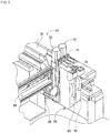
Fig. 3
Fig. 3 is a perspective view of a soldering device. -
Fig. 4
Fig. 4 is a block diagram showing a control device. -
Fig. 5
Fig. 5 is a schematic view showing a state in which molten solder is being flowed towards a lead inserted into a through-hole of a circuit board. -
Fig. 6
Fig. 6 is a schematic view showing a state in which the leaded component is being held by a suction nozzle even after flowing of the molten solder onto the lead has been completed. - The following describes in detail referring to the figures an example embodiment of the present invention.
-
Fig. 1 showscomponent mounter 10.Component mounter 10 performs work of mounting components oncircuit board 12.Component mounter 10 is provided with devicemain body 20, board conveying andholding device 22,component mounting device 24,mark camera 26,component camera 28,component supply device 30, loosecomponent supply device 32, soldering device (refer tofig. 3 ) 36, and control device (refer tofig. 4 ) 38. Note that, examples ofcircuit board 12 include circuit boards and boards with a three-dimensional construction, examples of a circuit board being a printed wiring board or a printed circuit board. - Device
main body 20 is configured fromframe section 40 andbeam section 42 that is mounted on theframe section 40. Board conveying andholding device 22 is positioned centrally insideframe section 40 in the front-rear direction, and includesconveyance device 50 andclamp device 52.Conveyance device 50conveys circuit board 12, andclamp device 52 holdscircuit board 12. Thus, board conveying and holdingdevice 22 conveyscircuit board 12 and holdscircuit board 12 at a specified position. Note that, in the descriptions below, the conveyance direction ofcircuit board 12 is referred to as the X direction, the direction horizontally perpendicular to the X direction is referred to as the Y direction, and the vertical direction is referred to as the Z direction. That is, the width direction ofcomponent mounter 10 is the X direction, and the front-rear direction is the Y direction. -
Component mounting device 24 is provided onbeam section 42, and includeswork heads head moving device 64. As shown infig. 2 ,suction nozzle 66 is provided on a lower surface of eachwork head suction nozzle 66. Further, workhead moving device 64 includesX-direction moving device 68, Y-direction moving device 70, and Z-direction moving device 72.Work heads frame 40 byX-direction moving device 68 and Y-direction moving device 70. Also,work heads sliders direction moving device 72 movessliders work heads direction moving device 72. - Mark
camera 26 is attached toslide 74 in a state facing downwards, and is moved in the X direction, Y direction, and Z direction together withwork head 60. Thus,mark camera 26 images any position onframe section 40. As shown infig. 1 ,component camera 28 is provided in a state facing upwards onframe section 40 between board conveying andholding device 22 andcomponent supply device 30. Thus,component camera 28 images a component held bysuction nozzle 66 ofwork heads -
Component supply device 30 is provided at an end offrame section 40 in the front-rear direction.Component supply device 30 includes tray-typecomponent supply device 78 and feeder-type component supply device (refer tofig. 4 ) 80. Tray-typecomponent supply device 78 supplies components in a state arranged in a tray. Feeder-type component supply 80 device supplies components via a tape feeder or stick feeder (not shown). - Loose
component supply device 32 is provided at the other end offrame section 40 in the front-rear direction. Loosecomponent supply device 32 lines up multiple components that are in a scattered state, and supplies the components in a lined-up state. That is, this device arranges multiple components that have random orientations to have a specified orientation and supplies the components in the specified orientation. Note that, components supplied bycomponent supply device 30 and loosecomponent supply device 32 may include electronic circuit components, configuration components of power modules, and the like. Also, electronic circuit components include components with leads and components without leads. -
Solder applying device 36 is arranged belowconveyance device 50, and as shown infig. 3 , includesflow device 100 and flowdevice moving device 102.Flow device 100 includessolder pot 106,flow nozzle 108, andnozzle cover 110. Solderpot 106 is a roughly rectangular parallelepiped with molten solder stored inside.Flow nozzle 108 is provided at the upper surface ofsolder pot 106. By operation of a pump (not shown), molten solder is pumped up fromsolder pot 106, such that molten solder flows upwards from the upper tip offlow nozzle 108.Nozzle cover 110 is roughly cylindrical and is provided at the upper surface ifsolder pot 106 so as to surroundflow nozzle 108. Thus, molten solder that flows from the upper end offlow nozzle 108 passes between the outer circumferential surface offlow nozzle 108 and the inner circumferential surface ofnozzle cover 110, and is circulated insidesolder pot 106. - Flow
device moving device 102 includesslider 112,X-direction moving device 114, Y-direction moving device 116, and Z-direction moving device 118.Slider 112 is roughly plate-shaped andflow device 100 is provided on an upper surface ofslider 112. Also,X-direction moving device 114 movesslider 112 in the conveyance direction ofcircuit board 12 byconveyance device 50, that is, the X direction; Y-direction moving device 116 movesslider 112 in the Y direction. Further, Z-direction moving device 118 movesslider 112 in the Z direction, that is, the vertical direction. By this,flow device 100 is moved to any position by operation of flowdevice moving device 102 underconveyance device 50. - Also, as shown in
fig. 4 ,control device 38 is provided withcontroller 152,multiple drive circuits 154, andimage processing device 156. Themultiple drive circuits 154 are connected toconveyance device 50,clamp device 52, work heads 60 and 62, workhead moving device 64, tray typecomponent supply device 78, feeder typecomponent supply device 80, loosecomponent supply device 32,flow device 100, and flowdevice moving device 102.Controller 152 is formed mainly from a computer, provided with a CPU, ROM, RAM, and so on, and connected to themultiple drive circuits 156. By this, operation of board conveying and holdingdevice 22,component mounting device 24, and so on is controlled bycontroller 152.Controller 152 is also connected toimage processing device 156.Image processing device 156 is for processing image data acquired bymark camera 26 andcomponent camera 28, andcontroller 152 acquires various information from the image data. -
Component mounter 10, according to the above configuration, mounts components oncircuit board 12 held by board conveying and holdingdevice 22. Withcomponent mounter 10, it is possible to mount various components tocircuit board 12; descriptions are given below of a case in which components with leads (hereinafter also referred to as "leaded component") are mounted oncircuit board 12. - Specifically,
circuit board 12 is conveyed to a work position, and is held at that position byclamp device 52. Next,mark camera 26 moves abovecircuit board 12 andimages circuit board 12. By this, information related to a holding position ofcircuit board 12 is obtained. Also,component supply device 30 or loosecomponent supply device 32 supplies components at a specified supply position. One of the work heads 60 or 62 moves above the component supply position and holds a component usingsuction nozzle 66. Note that, as shown infig. 5 ,leaded component 140 is configured from componentmain body section 142, and twoleads 144 protruding from the bottom surface of componentmain body section 142.Leaded component 140 is picked up and held by asuction nozzle 66 on the surface opposite to the bottom surface of componentmain body section 142. - Continuing,
work head leaded component 140 is moved abovecomponent camera 28, andleaded component 140 held bysuction nozzle 66 is imaged bycomponent camera 28. Accordingly, information related to the holding position of the component is obtained. Continuing,work head leaded component 140 moves abovecircuit board 12, and corrects the error in the holding position ofcircuit board 12 and the error in the holding position of the component and so on. Then, leads 144 ofleaded component 140 held bysuction nozzle 66 are inserted into through-holes formed incircuit board 12. - The insertion amount of
leads 144 is set for each type ofleaded component 140. Specifically, the insertion amount oflead 144 is set for each type ofleaded component 140, for example, for a case in which leads 144 are to be inserted into through-holes 148 such that the bottom surface of componentmain body section 142 ofleaded component 140 contacts the upper surface ofcircuit board 12, or for a case in which leads 144 are to be inserted into through-holes 148 such that a gap is maintained between the bottom surface of componentmain body section 142 ofleaded component 140 and the upper surface ofcircuit board 12. Descriptions here are for a case in which leads 144 are inserted into through-holes 148 such that a gap is maintained between the bottom surface of componentmain body section 142 ofleaded component 140 and the upper surface ofcircuit board 12, that is, for a case in which leads 144 are inserted into through-holes 148 such that componentmain body section 142 ofleaded component 140 is held in a state away fromcircuit board 12. - Further, when leads 144 are inserted into through-
holes 148 ofcircuit board 12,flow device 100 is moved below through-holes 148. Then, molten solder is flowed byflow device 100 towardsleads 144 ofleaded component 140 held bysuction nozzle 66 such that molten solder is applied to leads 144. In detail, when leads 144 ofleaded component 140 picked up and held bysuction nozzle 66 are inserted into through-holes 148 formed incircuit board 12,flow device 100 positioned below through-holes 148 is moved up such thatflow nozzle 108 offlow device 100 approaches the tip sections ofleads 144 inserted into through-holes 148. The approaching speed offlow nozzle 108, that is, raising speed V1 (mm/sec) offlow device 100, is set in advance. - Note that, with
flow device 100 positioned below through-hole 148, molten solder flows from the tip section offlow nozzle 108. Therefore, whenflow device 100 is raised to a specified height, as shown infig. 5 ,molten solder 150 flowing from the tip section offlow nozzle 108 is applied to the tip section of leads 144. In other words,molten solder 150 flows fromflow nozzle 108 towardsleads 144 ofleaded component 140 being held bysuction nozzle 66, such thatmolten solder 150 is applied to the tip sections ofleads 144 and to the through-holes ofcircuit board 12. Note that, the raising offlow device 100 is stopped when flow device has been raised to a specified height, andflow device 100 is maintained at that height. - Also, application time T1 (sec) for applying
molten solder 150 toleads 144 fromflow nozzle 108 is set in advance. Therefore, the elapsed time since starting application ofmolten solder 150 toleads 144 byflow nozzle 108, that is, the elapsed time sinceflow device 100 was raised to the specified height, is measured by a timer. Then, when the elapsed time has reached application time T1 (sec),flow device 100 is lowered. Note that, whenflow device 100 is lowered,molten solder 150 continues to flow fromflow nozzle 108. Thus, flownozzle 108 from whichmolten solder 150 is flowing is separated fromleads 144, then application ofmolten solder 150 toleads 144 is stopped. Note that, the speed from which flownozzle 108 separates fromleads 144 when application ofmolten solder 150 is complete, that is, lowering speed V2 (mm/sec) offlow device 100 is also set in advance. - Application time T1 of
molten solder 150, raising speed V1 offlow device 100, and lowering speed V2 offlow device 100 are set for each type ofleaded component 140 to which molten solder is to be applied, specifically, in accordance with the size, shape, capacity, and heat dissipation ratio ofleaded component 140, and the length, diameter, and the like of leads 144. By this, it is possible to apply an amount of molten solder to leads 144 in accordance with the type ofleaded component 140. - Further, holding time T2 (sec) is set in advance such that
leaded component 140 is held bysuction nozzle 66 even after application ofmolten solder 150 toleads 144 has been completed. Therefore, the elapsed time since completion of application ofmolten solder 150 toleads 144, that is, the elapsed time sinceflow device 100 was started to be lowered is measured by a timer. Then, when the elapsed time has reached holding time T2 (sec), holding ofleaded component 140 bysuction nozzle 66 is released. That is, as shown infig. 6 ,leaded component 140 is held bysuction nozzle 66 for a specified time even aftermolten solder 150 has finished being applied to leads 144. - Note that, holding time T2 (sec) is set as the time supposed to be required for the molten solder to harden after the completion of application of the
molten solder 150 and is set in accordance with factors such as the type of theleaded component 140 to which the molten solder is being applied, for example, the size, shape, thermal capacity, and heat dissipation ratio ofleaded component 140 and the length and diameter of leads 144. Holding time T2 (sec) may also be set in accordance with factors such as the insertion amount ofleads 144 into through-holes 148, the mounting orientation ofleaded component 140, the mounting position ofleaded component 140, and the required mounting accuracy ofleaded component 140. In this manner, by setting holding time T2 (sec),leaded component 140 is held bysuction nozzle 66 aftermolten solder 150 application to leads 144 has been completed untilmolten solder 150 hardens. - According to the above work,
leaded component 140 is mounted oncircuit board 12 with componentmain body 142 held in a state away fromcircuit board 12, with the mountedleaded component 140 being attached tocircuit board 12 via solder. Thus, by applying molten solder to leads 144 inserted into through-holes 148 and to the location oncircuit board 12 at which leads 144 are inserted, an electrical connection is completed betweenleads 144 andcircuit board 12, thus forming an electrical circuit. - In this manner,
component mounter 10 is provided withcomponent mounting device 24 that performs mounting work, andsoldering device 36 that performs soldering work. Thus, it is possible to mount aleaded component 140 oncircuit board 12 and to solder theleaded component 140 to thecircuit board 12 in asingle component mounter 10. Also, by applying molten solder toleaded component 140 being held bysuction nozzle 66 and holdingleaded component 140 for which application of molten solder is complete bysuction nozzle 66, it is possible to solderleaded component 140 at a planned mounting position with high accuracy. - In contrast, conventionally, mounting work and soldering work are performed respectively by a mounting work machine provided with
component mounting device 24 and a soldering machine provided with a soldering device. Therefore, at least two work machines are required to mount the leaded component tocircuit board 12 and to solder the mountedleaded component 140 tocircuit board 12. Further, when performing soldering work withsoldering device 36 in a soldering machine, there is a tendency forleaded component 140 mounted oncircuit board 12 to shift due to the flowing molten solder. And, usually, the internal diameter of through-holes 148 into which leads 144 are inserted is larger than the external diameter ofleads 144, so there is a tendency for positional deviation to occur ofleads 144 in through-holes 148 due to the flowing molten solder. Further, not only when molten solder is flowing, but also after flowing of the molten solder is complete, due to the surface tension that occurs as the molten solder is hardening, there is a tendency for positional deviation of theleaded component 140 or raising up of theleaded component 140 to occur. When such positional deviation of theleaded component 140 or raising up of theleaded component 140 occurs, the mounting accuracy of theleaded component 140 worsens, worsening the quality ofcircuit board 12. Therefore, with a conventional work machine, it is necessary to curtail positional deviation ofleaded component 140 and raising up ofleaded component 140, thus, afterleaded component 140 has been mounted oncircuit board 12, it is necessary to use a jig or the like to fix theleaded component 140 the leads of which have been inserted into through-holes 148. In other words, it is necessary to perform work of fixingleaded component 140 that has been mounted oncircuit board 12 during mounting work and soldering work. - However, with
component mounter 10, as described above, it is possible to mountleaded component 140 ontocircuit board 12 and to solder thatleaded component 140 to thecircuit board 12. By this, it is possible to reduce the quantity of work machines, reduce costs, and reduce the space required to install work machines. Also, because it is not necessary to conveycircuit board 12 between work machines, work time is shorter. - Further, with
component mounter 10, molten solder is applied to aleaded component 140 in a state being held bysuction nozzle 66. Thus, there is no problem withleaded component 140 raising or with positional deviation ofleaded component 140 due to flowing molten solder. Also, even after molten solder has finished being applied toleads 144,leaded component 40 is held continuously for a specified time bysuction nozzle 66. Thus, there is no problem withleaded component 140 raising or with positional deviation ofleaded component 140 due to hardening of molten solder. Accordingly, it is possible to perform soldering ofleaded component 140 tocircuit board 12 highly accurately afterleaded component 140 has been mounted oncircuit board 12 without the need to perform holding work of holdingleaded component 140 using a jig or the like. - Also, as shown in
fig. 4 ,controller 152 ofcontrol device 38 includesinsertion section 160,application section 162, and holdingrelease section 164.Insertion section 160 is for insertingleaded component 140 into through-holes 148.Application section 162 is a functional section for applying molten solder to leads 144 inserted into through-holes 148. Holdingrelease section 164 is a functional section for releasing the holding ofleaded component 140 bysuction nozzle 66 after holding time T2 (sec) has elapsed from the completion of application of the molten solder. - In an embodiment above,
component mounter 10 is an example of a board work machine.Component mounting device 24 is an example of a holding device.Soldering device 36 is an example of an application device.Control device 38 is an example of a control device.Insertion section 160 is an example of an insertion section.Application 162 is an example of an application section. Holdingrelease section 164 is an example of a holding release section. Further, processing performed byinsertion section 160 is an example of inserting processing. Processing performed byapplication section 162 is an example of applying processing. Processing performed by holdingrelease section 164 is an example of holding releasing processing. - Further, the present invention is not limited to the above example embodiments, and various changed or improved methods of embodiment are possible based on the knowledge of someone skilled in the art. Specifically, for example, in an embodiment above, during soldering work, molten solder is flowed towards
leads 144, however, molten solder may be applied toleads 144 using various methods. Specifically, for example, leads 144 may be dipped in molten solder, or a member dipped in molten solder may be contacted against leads 144. - Also, in an embodiment above,
leaded component 140 is inserted intocircuit board 12 from above and molten solder is applied from belowcircuit board 12, butleaded component 140 may be inserted intocircuit board 12 from below and molten solder may be applied from abovecircuit board 12 When applying molten solder from abovecircuit board 12, the molten solder may be dripped onto leads 144. - Further, in an embodiment above,
leaded component 140 is mounted oncircuit board 12 with componentmain body section 142 held in a state away fromcircuit board 12, butleaded component 140 may be mounted oncircuit board 12 with componentmain body section 142 contactingcircuit board 12. With aleaded component 140 mounted in this manner too, when the molten solder hardens, because surface tension and the like tends to cause positional deviation ofleaded component 140, it is beneficial to continue holdingleaded component 140 withsuction nozzle 66 after application of molten solder has been completed. - Further, in an embodiment above, a timer starts measuring time from when application of molten solder is complete, but the timer may start timing at various points. For example, the timer may start timing from when application of molten solder is started. However, when the timer starts timing from when application of molten solder is started, holding time T2 (sec) is set such that
leaded component 140 continues to be held bysuction nozzle 66 even after application of molten solder has been completed. In other words, holding time T2 (sec) is set to be longer than application time T1 (sec). - Also, in an embodiment above, through-
hole 148 is used as a through-hole, but a through-hole may include a notch or the like, so long as it piercescircuit board 12 in a vertical direction. -
- 10:
- component mounter (board work machine);
- 24:
- component mounting device (holding device);
- 36:
- soldering device (applying device);
- 38:
- control device;
- 160:
- insertion section;
- 162:
- application section;
- 164:
- holding release section
Claims (4)
- A board work machine comprising:a holding device configured to hold a leaded component having a lead and insert the lead into a through-hole formed in a board;an applying device configured to apply molten solder to the lead inserted into the through-hole; anda control device, the control device being provided with
an insertion section configured to cause the holding device to insert the lead into the through-hole;
an application section configured to cause the applying device to apply molten solder to the lead of the leaded component while the leaded component is being held by the holding device; and
a holding release section configured to set a setting time for the leaded component to be held by the holding device after the applying device has completed applying molten solder to the lead and to cause the holding device to release the leaded component after the setting time has elapsed. - The board work machine according to claim 1, wherein
the setting time is set for each type of leaded component to be held by the holding device. - The board work machine according to claim 1 or 2, wherein
the holding release device is configured to cause the holding device to release the leaded component after the setting time has elapsed following the completion of the applying molten solder by the applying device. - An insertion method for inserting a leaded component into a board using a board work machine provided with a holding device configured to hold a leaded component having a lead and insert the lead into a through-hole formed in a board, and an applying device configured to apply molten solder to the lead inserted into the through-hole, the insertion method comprising:inserting the lead into the through-hole using the holding device;applying molten to the lead of the leaded component using the applying device while the leaded component is being held by the holding device;setting a setting time for the leaded component to be held by the holding device after the applying device has completed applying molten solder to the lead; andreleasing the leaded component from holding by the holding device after the setting time has elapsed.
Applications Claiming Priority (1)
| Application Number | Priority Date | Filing Date | Title |
|---|---|---|---|
| PCT/JP2016/079142 WO2018061207A1 (en) | 2016-09-30 | 2016-09-30 | Machine for performing work on substrate, and insertion method |
Publications (3)
| Publication Number | Publication Date |
|---|---|
| EP3522687A1 true EP3522687A1 (en) | 2019-08-07 |
| EP3522687A4 EP3522687A4 (en) | 2020-07-08 |
| EP3522687B1 EP3522687B1 (en) | 2023-07-19 |
Family
ID=61760230
Family Applications (1)
| Application Number | Title | Priority Date | Filing Date |
|---|---|---|---|
| EP16917757.3A Active EP3522687B1 (en) | 2016-09-30 | 2016-09-30 | Machine for performing work on substrate, and insertion method |
Country Status (4)
| Country | Link |
|---|---|
| EP (1) | EP3522687B1 (en) |
| JP (1) | JP6759348B2 (en) |
| CN (1) | CN109792844A (en) |
| WO (1) | WO2018061207A1 (en) |
Families Citing this family (4)
| Publication number | Priority date | Publication date | Assignee | Title |
|---|---|---|---|---|
| CN112518160A (en) * | 2020-11-23 | 2021-03-19 | 武汉光迅科技股份有限公司 | Substrate assembly method and system |
| CN112687550B (en) * | 2020-12-28 | 2024-05-17 | 池州巨成电子科技有限公司 | Semiconductor wafer packaging equipment for power chip production and production process |
| CN113084342A (en) * | 2021-03-10 | 2021-07-09 | 联想(北京)有限公司 | Laser welding method |
| DE102022109905A1 (en) * | 2021-04-26 | 2022-10-27 | Pac Tech - Packaging Technologies Gmbh | Method and apparatus for soldering an electronic component to a circuit board, computer program product and computer-readable medium |
Family Cites Families (8)
| Publication number | Priority date | Publication date | Assignee | Title |
|---|---|---|---|---|
| JPH10209622A (en) * | 1997-01-27 | 1998-08-07 | Denso Corp | How to mount insertable parts |
| JP2003051671A (en) * | 2001-06-01 | 2003-02-21 | Nec Corp | Manufacturing method of mounting structure and mounting structure |
| KR101890825B1 (en) * | 2009-03-10 | 2018-08-22 | 존스테크 인터내셔널 코포레이션 | Electrically Conductive Pins For Microcircuit Tester |
| JP2011254034A (en) * | 2010-06-04 | 2011-12-15 | Fuji Electric Co Ltd | Flow soldering method |
| CN202435791U (en) * | 2011-12-23 | 2012-09-12 | 东莞市新泽谷机械制造股份有限公司 | Vertical plug-in machine head plug-in mechanism |
| WO2014045370A1 (en) * | 2012-09-20 | 2014-03-27 | 富士機械製造株式会社 | Work machine for printed circuit boards and mounting method |
| JP2014130948A (en) * | 2012-12-28 | 2014-07-10 | Toshiba Corp | Component mounting device, component mounting system, and component mounting method |
| JP6521990B2 (en) * | 2014-10-06 | 2019-05-29 | 株式会社Fuji | Board-to-board work machine and mounting method |
-
2016
- 2016-09-30 CN CN201680089556.XA patent/CN109792844A/en active Pending
- 2016-09-30 EP EP16917757.3A patent/EP3522687B1/en active Active
- 2016-09-30 WO PCT/JP2016/079142 patent/WO2018061207A1/en not_active Ceased
- 2016-09-30 JP JP2018541854A patent/JP6759348B2/en active Active
Also Published As
| Publication number | Publication date |
|---|---|
| JPWO2018061207A1 (en) | 2019-07-18 |
| EP3522687A4 (en) | 2020-07-08 |
| JP6759348B2 (en) | 2020-09-23 |
| CN109792844A (en) | 2019-05-21 |
| EP3522687B1 (en) | 2023-07-19 |
| WO2018061207A1 (en) | 2018-04-05 |
Similar Documents
| Publication | Publication Date | Title |
|---|---|---|
| EP3522687B1 (en) | Machine for performing work on substrate, and insertion method | |
| CN104206033B (en) | Ball loading method and substrate working machine | |
| US11304350B2 (en) | Board work machine and insertion method | |
| JP2007110170A (en) | Electronic component mounting method, apparatus, and electronic component mounting data creation method | |
| US20190254174A1 (en) | Component mounting method, component mounting system, and manufacturing method of component mounting board | |
| EP3493658B1 (en) | Soldering device | |
| CN109792859B (en) | Component Mounter | |
| US10470350B2 (en) | Work machine | |
| US10506750B2 (en) | Board work machine and recognition method | |
| JP7644119B2 (en) | Coating equipment and component placement machines | |
| JP6654978B2 (en) | Board work machine | |
| CN114787974B (en) | Component mounting machine and transfer material transfer method | |
| EP3346812A1 (en) | Operation machine | |
| US10959361B2 (en) | Substrate working machine | |
| JP7167252B2 (en) | Work system and information processing equipment | |
| JP3983275B2 (en) | Electronic component mounting method and apparatus | |
| US12414280B2 (en) | Substrate working machine | |
| CN210444746U (en) | Holding tool, storage device, and work machine | |
| US20220007559A1 (en) | Work machine | |
| WO2018216076A1 (en) | Board working machine |
Legal Events
| Date | Code | Title | Description |
|---|---|---|---|
| STAA | Information on the status of an ep patent application or granted ep patent |
Free format text: STATUS: THE INTERNATIONAL PUBLICATION HAS BEEN MADE |
|
| PUAI | Public reference made under article 153(3) epc to a published international application that has entered the european phase |
Free format text: ORIGINAL CODE: 0009012 |
|
| STAA | Information on the status of an ep patent application or granted ep patent |
Free format text: STATUS: REQUEST FOR EXAMINATION WAS MADE |
|
| 17P | Request for examination filed |
Effective date: 20190325 |
|
| AK | Designated contracting states |
Kind code of ref document: A1 Designated state(s): AL AT BE BG CH CY CZ DE DK EE ES FI FR GB GR HR HU IE IS IT LI LT LU LV MC MK MT NL NO PL PT RO RS SE SI SK SM TR |
|
| AX | Request for extension of the european patent |
Extension state: BA ME |
|
| DAV | Request for validation of the european patent (deleted) | ||
| DAX | Request for extension of the european patent (deleted) | ||
| A4 | Supplementary search report drawn up and despatched |
Effective date: 20200608 |
|
| RIC1 | Information provided on ipc code assigned before grant |
Ipc: H05K 3/34 20060101AFI20200602BHEP Ipc: B23K 1/00 20060101ALI20200602BHEP |
|
| STAA | Information on the status of an ep patent application or granted ep patent |
Free format text: STATUS: EXAMINATION IS IN PROGRESS |
|
| 17Q | First examination report despatched |
Effective date: 20210503 |
|
| GRAP | Despatch of communication of intention to grant a patent |
Free format text: ORIGINAL CODE: EPIDOSNIGR1 |
|
| STAA | Information on the status of an ep patent application or granted ep patent |
Free format text: STATUS: GRANT OF PATENT IS INTENDED |
|
| INTG | Intention to grant announced |
Effective date: 20230130 |
|
| GRAJ | Information related to disapproval of communication of intention to grant by the applicant or resumption of examination proceedings by the epo deleted |
Free format text: ORIGINAL CODE: EPIDOSDIGR1 |
|
| STAA | Information on the status of an ep patent application or granted ep patent |
Free format text: STATUS: EXAMINATION IS IN PROGRESS |
|
| GRAP | Despatch of communication of intention to grant a patent |
Free format text: ORIGINAL CODE: EPIDOSNIGR1 |
|
| STAA | Information on the status of an ep patent application or granted ep patent |
Free format text: STATUS: GRANT OF PATENT IS INTENDED |
|
| INTC | Intention to grant announced (deleted) | ||
| INTG | Intention to grant announced |
Effective date: 20230411 |
|
| GRAS | Grant fee paid |
Free format text: ORIGINAL CODE: EPIDOSNIGR3 |
|
| P01 | Opt-out of the competence of the unified patent court (upc) registered |
Effective date: 20230328 |
|
| GRAA | (expected) grant |
Free format text: ORIGINAL CODE: 0009210 |
|
| STAA | Information on the status of an ep patent application or granted ep patent |
Free format text: STATUS: THE PATENT HAS BEEN GRANTED |
|
| AK | Designated contracting states |
Kind code of ref document: B1 Designated state(s): AL AT BE BG CH CY CZ DE DK EE ES FI FR GB GR HR HU IE IS IT LI LT LU LV MC MK MT NL NO PL PT RO RS SE SI SK SM TR |
|
| REG | Reference to a national code |
Ref country code: GB Ref legal event code: FG4D |
|
| REG | Reference to a national code |
Ref country code: CH Ref legal event code: EP |
|
| REG | Reference to a national code |
Ref country code: DE Ref legal event code: R096 Ref document number: 602016081256 Country of ref document: DE |
|
| REG | Reference to a national code |
Ref country code: IE Ref legal event code: FG4D |
|
| REG | Reference to a national code |
Ref country code: LT Ref legal event code: MG9D |
|
| REG | Reference to a national code |
Ref country code: NL Ref legal event code: MP Effective date: 20230719 |
|
| REG | Reference to a national code |
Ref country code: AT Ref legal event code: MK05 Ref document number: 1590793 Country of ref document: AT Kind code of ref document: T Effective date: 20230719 |
|
| PG25 | Lapsed in a contracting state [announced via postgrant information from national office to epo] |
Ref country code: NL Free format text: LAPSE BECAUSE OF FAILURE TO SUBMIT A TRANSLATION OF THE DESCRIPTION OR TO PAY THE FEE WITHIN THE PRESCRIBED TIME-LIMIT Effective date: 20230719 |
|
| PG25 | Lapsed in a contracting state [announced via postgrant information from national office to epo] |
Ref country code: GR Free format text: LAPSE BECAUSE OF FAILURE TO SUBMIT A TRANSLATION OF THE DESCRIPTION OR TO PAY THE FEE WITHIN THE PRESCRIBED TIME-LIMIT Effective date: 20231020 |
|
| PG25 | Lapsed in a contracting state [announced via postgrant information from national office to epo] |
Ref country code: IS Free format text: LAPSE BECAUSE OF FAILURE TO SUBMIT A TRANSLATION OF THE DESCRIPTION OR TO PAY THE FEE WITHIN THE PRESCRIBED TIME-LIMIT Effective date: 20231119 |
|
| PG25 | Lapsed in a contracting state [announced via postgrant information from national office to epo] |
Ref country code: SE Free format text: LAPSE BECAUSE OF FAILURE TO SUBMIT A TRANSLATION OF THE DESCRIPTION OR TO PAY THE FEE WITHIN THE PRESCRIBED TIME-LIMIT Effective date: 20230719 Ref country code: RS Free format text: LAPSE BECAUSE OF FAILURE TO SUBMIT A TRANSLATION OF THE DESCRIPTION OR TO PAY THE FEE WITHIN THE PRESCRIBED TIME-LIMIT Effective date: 20230719 Ref country code: PT Free format text: LAPSE BECAUSE OF FAILURE TO SUBMIT A TRANSLATION OF THE DESCRIPTION OR TO PAY THE FEE WITHIN THE PRESCRIBED TIME-LIMIT Effective date: 20231120 Ref country code: NO Free format text: LAPSE BECAUSE OF FAILURE TO SUBMIT A TRANSLATION OF THE DESCRIPTION OR TO PAY THE FEE WITHIN THE PRESCRIBED TIME-LIMIT Effective date: 20231019 Ref country code: LV Free format text: LAPSE BECAUSE OF FAILURE TO SUBMIT A TRANSLATION OF THE DESCRIPTION OR TO PAY THE FEE WITHIN THE PRESCRIBED TIME-LIMIT Effective date: 20230719 Ref country code: LT Free format text: LAPSE BECAUSE OF FAILURE TO SUBMIT A TRANSLATION OF THE DESCRIPTION OR TO PAY THE FEE WITHIN THE PRESCRIBED TIME-LIMIT Effective date: 20230719 Ref country code: IS Free format text: LAPSE BECAUSE OF FAILURE TO SUBMIT A TRANSLATION OF THE DESCRIPTION OR TO PAY THE FEE WITHIN THE PRESCRIBED TIME-LIMIT Effective date: 20231119 Ref country code: HR Free format text: LAPSE BECAUSE OF FAILURE TO SUBMIT A TRANSLATION OF THE DESCRIPTION OR TO PAY THE FEE WITHIN THE PRESCRIBED TIME-LIMIT Effective date: 20230719 Ref country code: GR Free format text: LAPSE BECAUSE OF FAILURE TO SUBMIT A TRANSLATION OF THE DESCRIPTION OR TO PAY THE FEE WITHIN THE PRESCRIBED TIME-LIMIT Effective date: 20231020 Ref country code: FI Free format text: LAPSE BECAUSE OF FAILURE TO SUBMIT A TRANSLATION OF THE DESCRIPTION OR TO PAY THE FEE WITHIN THE PRESCRIBED TIME-LIMIT Effective date: 20230719 Ref country code: AT Free format text: LAPSE BECAUSE OF FAILURE TO SUBMIT A TRANSLATION OF THE DESCRIPTION OR TO PAY THE FEE WITHIN THE PRESCRIBED TIME-LIMIT Effective date: 20230719 |
|
| PG25 | Lapsed in a contracting state [announced via postgrant information from national office to epo] |
Ref country code: PL Free format text: LAPSE BECAUSE OF FAILURE TO SUBMIT A TRANSLATION OF THE DESCRIPTION OR TO PAY THE FEE WITHIN THE PRESCRIBED TIME-LIMIT Effective date: 20230719 |
|
| REG | Reference to a national code |
Ref country code: DE Ref legal event code: R097 Ref document number: 602016081256 Country of ref document: DE |
|
| PG25 | Lapsed in a contracting state [announced via postgrant information from national office to epo] |
Ref country code: ES Free format text: LAPSE BECAUSE OF FAILURE TO SUBMIT A TRANSLATION OF THE DESCRIPTION OR TO PAY THE FEE WITHIN THE PRESCRIBED TIME-LIMIT Effective date: 20230719 |
|
| PG25 | Lapsed in a contracting state [announced via postgrant information from national office to epo] |
Ref country code: SM Free format text: LAPSE BECAUSE OF FAILURE TO SUBMIT A TRANSLATION OF THE DESCRIPTION OR TO PAY THE FEE WITHIN THE PRESCRIBED TIME-LIMIT Effective date: 20230719 Ref country code: RO Free format text: LAPSE BECAUSE OF FAILURE TO SUBMIT A TRANSLATION OF THE DESCRIPTION OR TO PAY THE FEE WITHIN THE PRESCRIBED TIME-LIMIT Effective date: 20230719 Ref country code: ES Free format text: LAPSE BECAUSE OF FAILURE TO SUBMIT A TRANSLATION OF THE DESCRIPTION OR TO PAY THE FEE WITHIN THE PRESCRIBED TIME-LIMIT Effective date: 20230719 Ref country code: EE Free format text: LAPSE BECAUSE OF FAILURE TO SUBMIT A TRANSLATION OF THE DESCRIPTION OR TO PAY THE FEE WITHIN THE PRESCRIBED TIME-LIMIT Effective date: 20230719 Ref country code: DK Free format text: LAPSE BECAUSE OF FAILURE TO SUBMIT A TRANSLATION OF THE DESCRIPTION OR TO PAY THE FEE WITHIN THE PRESCRIBED TIME-LIMIT Effective date: 20230719 Ref country code: CZ Free format text: LAPSE BECAUSE OF FAILURE TO SUBMIT A TRANSLATION OF THE DESCRIPTION OR TO PAY THE FEE WITHIN THE PRESCRIBED TIME-LIMIT Effective date: 20230719 Ref country code: SK Free format text: LAPSE BECAUSE OF FAILURE TO SUBMIT A TRANSLATION OF THE DESCRIPTION OR TO PAY THE FEE WITHIN THE PRESCRIBED TIME-LIMIT Effective date: 20230719 |
|
| REG | Reference to a national code |
Ref country code: CH Ref legal event code: PL |
|
| PG25 | Lapsed in a contracting state [announced via postgrant information from national office to epo] |
Ref country code: LU Free format text: LAPSE BECAUSE OF NON-PAYMENT OF DUE FEES Effective date: 20230930 |
|
| PLBE | No opposition filed within time limit |
Free format text: ORIGINAL CODE: 0009261 |
|
| STAA | Information on the status of an ep patent application or granted ep patent |
Free format text: STATUS: NO OPPOSITION FILED WITHIN TIME LIMIT |
|
| REG | Reference to a national code |
Ref country code: BE Ref legal event code: MM Effective date: 20230930 |
|
| PG25 | Lapsed in a contracting state [announced via postgrant information from national office to epo] |
Ref country code: LU Free format text: LAPSE BECAUSE OF NON-PAYMENT OF DUE FEES Effective date: 20230930 Ref country code: IT Free format text: LAPSE BECAUSE OF FAILURE TO SUBMIT A TRANSLATION OF THE DESCRIPTION OR TO PAY THE FEE WITHIN THE PRESCRIBED TIME-LIMIT Effective date: 20230719 Ref country code: MC Free format text: LAPSE BECAUSE OF FAILURE TO SUBMIT A TRANSLATION OF THE DESCRIPTION OR TO PAY THE FEE WITHIN THE PRESCRIBED TIME-LIMIT Effective date: 20230719 |
|
| 26N | No opposition filed |
Effective date: 20240422 |
|
| GBPC | Gb: european patent ceased through non-payment of renewal fee |
Effective date: 20231019 |
|
| REG | Reference to a national code |
Ref country code: IE Ref legal event code: MM4A |
|
| PG25 | Lapsed in a contracting state [announced via postgrant information from national office to epo] |
Ref country code: IE Free format text: LAPSE BECAUSE OF NON-PAYMENT OF DUE FEES Effective date: 20230930 |
|
| PG25 | Lapsed in a contracting state [announced via postgrant information from national office to epo] |
Ref country code: GB Free format text: LAPSE BECAUSE OF NON-PAYMENT OF DUE FEES Effective date: 20231019 |
|
| PG25 | Lapsed in a contracting state [announced via postgrant information from national office to epo] |
Ref country code: CH Free format text: LAPSE BECAUSE OF NON-PAYMENT OF DUE FEES Effective date: 20230930 |
|
| PG25 | Lapsed in a contracting state [announced via postgrant information from national office to epo] |
Ref country code: IE Free format text: LAPSE BECAUSE OF NON-PAYMENT OF DUE FEES Effective date: 20230930 Ref country code: GB Free format text: LAPSE BECAUSE OF NON-PAYMENT OF DUE FEES Effective date: 20231019 Ref country code: FR Free format text: LAPSE BECAUSE OF NON-PAYMENT OF DUE FEES Effective date: 20230930 Ref country code: CH Free format text: LAPSE BECAUSE OF NON-PAYMENT OF DUE FEES Effective date: 20230930 Ref country code: SI Free format text: LAPSE BECAUSE OF FAILURE TO SUBMIT A TRANSLATION OF THE DESCRIPTION OR TO PAY THE FEE WITHIN THE PRESCRIBED TIME-LIMIT Effective date: 20230719 |
|
| PG25 | Lapsed in a contracting state [announced via postgrant information from national office to epo] |
Ref country code: BE Free format text: LAPSE BECAUSE OF NON-PAYMENT OF DUE FEES Effective date: 20230930 |
|
| PG25 | Lapsed in a contracting state [announced via postgrant information from national office to epo] |
Ref country code: BG Free format text: LAPSE BECAUSE OF FAILURE TO SUBMIT A TRANSLATION OF THE DESCRIPTION OR TO PAY THE FEE WITHIN THE PRESCRIBED TIME-LIMIT Effective date: 20230719 |
|
| PG25 | Lapsed in a contracting state [announced via postgrant information from national office to epo] |
Ref country code: BG Free format text: LAPSE BECAUSE OF FAILURE TO SUBMIT A TRANSLATION OF THE DESCRIPTION OR TO PAY THE FEE WITHIN THE PRESCRIBED TIME-LIMIT Effective date: 20230719 |
|
| PG25 | Lapsed in a contracting state [announced via postgrant information from national office to epo] |
Ref country code: CY Free format text: LAPSE BECAUSE OF FAILURE TO SUBMIT A TRANSLATION OF THE DESCRIPTION OR TO PAY THE FEE WITHIN THE PRESCRIBED TIME-LIMIT; INVALID AB INITIO Effective date: 20160930 |
|
| PG25 | Lapsed in a contracting state [announced via postgrant information from national office to epo] |
Ref country code: HU Free format text: LAPSE BECAUSE OF FAILURE TO SUBMIT A TRANSLATION OF THE DESCRIPTION OR TO PAY THE FEE WITHIN THE PRESCRIBED TIME-LIMIT; INVALID AB INITIO Effective date: 20160930 |
|
| PGFP | Annual fee paid to national office [announced via postgrant information from national office to epo] |
Ref country code: DE Payment date: 20250805 Year of fee payment: 10 |
|
| PG25 | Lapsed in a contracting state [announced via postgrant information from national office to epo] |
Ref country code: TR Free format text: LAPSE BECAUSE OF FAILURE TO SUBMIT A TRANSLATION OF THE DESCRIPTION OR TO PAY THE FEE WITHIN THE PRESCRIBED TIME-LIMIT Effective date: 20230719 |