EP3522297A1 - Wide angle coverage antenna - Google Patents
Wide angle coverage antenna Download PDFInfo
- Publication number
- EP3522297A1 EP3522297A1 EP19152734.0A EP19152734A EP3522297A1 EP 3522297 A1 EP3522297 A1 EP 3522297A1 EP 19152734 A EP19152734 A EP 19152734A EP 3522297 A1 EP3522297 A1 EP 3522297A1
- Authority
- EP
- European Patent Office
- Prior art keywords
- conductive
- antenna device
- patches
- transmission line
- coupled
- Prior art date
- Legal status (The legal status is an assumption and is not a legal conclusion. Google has not performed a legal analysis and makes no representation as to the accuracy of the status listed.)
- Granted
Links
Images


Classifications
-
- H—ELECTRICITY
- H01—ELECTRIC ELEMENTS
- H01Q—ANTENNAS, i.e. RADIO AERIALS
- H01Q21/00—Antenna arrays or systems
- H01Q21/06—Arrays of individually energised antenna units similarly polarised and spaced apart
- H01Q21/061—Two dimensional planar arrays
- H01Q21/065—Patch antenna array
-
- H—ELECTRICITY
- H01—ELECTRIC ELEMENTS
- H01Q—ANTENNAS, i.e. RADIO AERIALS
- H01Q1/00—Details of, or arrangements associated with, antennas
- H01Q1/27—Adaptation for use in or on movable bodies
- H01Q1/32—Adaptation for use in or on road or rail vehicles
- H01Q1/3208—Adaptation for use in or on road or rail vehicles characterised by the application wherein the antenna is used
- H01Q1/3233—Adaptation for use in or on road or rail vehicles characterised by the application wherein the antenna is used particular used as part of a sensor or in a security system, e.g. for automotive radar, navigation systems
-
- H—ELECTRICITY
- H01—ELECTRIC ELEMENTS
- H01Q—ANTENNAS, i.e. RADIO AERIALS
- H01Q1/00—Details of, or arrangements associated with, antennas
- H01Q1/36—Structural form of radiating elements, e.g. cone, spiral, umbrella; Particular materials used therewith
- H01Q1/38—Structural form of radiating elements, e.g. cone, spiral, umbrella; Particular materials used therewith formed by a conductive layer on an insulating support
-
- H—ELECTRICITY
- H01—ELECTRIC ELEMENTS
- H01Q—ANTENNAS, i.e. RADIO AERIALS
- H01Q13/00—Waveguide horns or mouths; Slot antennas; Leaky-waveguide antennas; Equivalent structures causing radiation along the transmission path of a guided wave
- H01Q13/20—Non-resonant leaky-waveguide or transmission-line antennas; Equivalent structures causing radiation along the transmission path of a guided wave
- H01Q13/206—Microstrip transmission line antennas
-
- H—ELECTRICITY
- H01—ELECTRIC ELEMENTS
- H01Q—ANTENNAS, i.e. RADIO AERIALS
- H01Q15/00—Devices for reflection, refraction, diffraction or polarisation of waves radiated from an antenna, e.g. quasi-optical devices
- H01Q15/0006—Devices acting selectively as reflecting surface, as diffracting or as refracting device, e.g. frequency filtering or angular spatial filtering devices
- H01Q15/006—Selective devices having photonic band gap materials or materials of which the material properties are frequency dependent, e.g. perforated substrates, high-impedance surfaces
- H01Q15/008—Selective devices having photonic band gap materials or materials of which the material properties are frequency dependent, e.g. perforated substrates, high-impedance surfaces said selective devices having Sievenpipers' mushroom elements
-
- H—ELECTRICITY
- H01—ELECTRIC ELEMENTS
- H01Q—ANTENNAS, i.e. RADIO AERIALS
- H01Q5/00—Arrangements for simultaneous operation of antennas on two or more different wavebands, e.g. dual-band or multi-band arrangements
- H01Q5/30—Arrangements for providing operation on different wavebands
- H01Q5/378—Combination of fed elements with parasitic elements
- H01Q5/385—Two or more parasitic elements
Definitions
- Radar and lidar sensing devices provide the capability to detect objects in a vicinity or pathway of the vehicle. Many such devices include a radiating antenna that emits the radiation used for object detection.
- antennas that are useful for short or medium range detection have the capability of covering a wide field of view, but experience high loss when the electromagnetic wave radiated from the antenna passes through the fascia of the vehicle. Such high losses are typically associated with vertical polarization of the antenna.
- One attempt to address that problem is to incorporate horizontal polarization.
- the difficulty associated with horizontal polarization is that the impedance bandwidth is typically too narrow to satisfy production requirements.
- One approach to increase the impedance bandwidth includes increasing the thickness of the antenna substrate material. A disadvantage associated with that approach is that it increases cost.
- Another difficulty associated with some known radar antenna configurations is the occurrence of high frequency ripples resulting from radiation scattering from nearby antennas, electronic components on the vehicle, and other metal or dielectric materials in close proximity to the antennas.
- a further complication is that the ripples in the radiation pattern for each antenna occur at different angles and that affects the uniformity of the radiation patterns of all the antennas used for radar.
- a non-uniform radiation pattern significantly lowers the angle finding accuracy of the radar system.
- An illustrative example antenna device includes a substrate, a transmission line supported on the substrate, and a plurality of conductive patches supported on the substrate. Each conductive patch has a first end coupled to the transmission line and a second end coupled to ground. The plurality of conductive patches are arranged in sets including two of the conductive patches facing each other on opposite sides of the transmission line.
- the conductive patches respectively have a distance between the first end and the second end, and an operating frequency of the antenna device is based on the distance.
- the conductive patches respectively have a first width near the first end and a radiating power of the conductive patches, respectively, is based on the width.
- the conductive patches respectively have a second width near the second end and the second width is different than the first width.
- the first width of two of the conductive patches is different than the first width of two others of the conductive patches.
- the two of the conductive patches are closer to a first end of the transmission line; the two others of the conductive patches are closer to a second, opposite end of the transmission line; and the first end of the transmission line is coupled to a source of radiation.
- a radiating power of the conductive patches, respectively, is based on the second width.
- the conductive patches are situated on one side of the substrate, the substrate includes a grounding layer spaced from the one side of the substrate, and the conductive patches respectively include a plurality of conductive vias coupled to the grounding layer.
- a length between the second ends of the conductive patches in each set corresponds to a one-half wavelength in the substrate of radiation radiated by the conductive patches.
- An example embodiment having one or more features of the antenna device of any of the previous paragraphs includes a conductive layer near the conductive patches and a plurality of conductive vias coupled between the conductive layer and ground.
- the conductive layer may comprise a continuous layer of conductive material
- the conductive layer comprises a plurality of parasitic conductive elements and each of the parasitic conductive elements is coupled with one of the conductive vias.
- each conductive via is situated in a position relative to edges of a coupled one of the parasitic conductive elements and the position of some of the vias is different than the position of others of the vias.
- the parasitic conductive elements coupled to the some of the vias are closer to the conductive patches than the parasitic conductive elements coupled to the others of the vias, and the respective position of the others of the vias is closer to a center of the respective coupled parasitic conductive elements than the position of the some of the vias.
- the conductive layer is coupled to the second ends of the conductive patches and the conductive layer has a dimension parallel to the transmission line that is at least as long as the transmission line.
- the conductive patches are on one surface of the substrate and the conductive layer is on the one surface of the substrate.
- the transmission line comprises a differential twin line.
- An example embodiment having one or more features of the antenna device of any of the previous paragraphs includes a source of radiation that provides an unbalanced signal and a transition coupling the source of radiation to the transmission line. The transition balances the unbalanced signal before the signal propagates along the transmission line.
- the source of radiation comprises a substrate integrated waveguide and the transition comprises a balun.
- the conductive patches each have a geometric configuration and the geometric configuration of the two conductive patches in each set is the same.
- Embodiments of this invention provide an antenna including a transmission line and a plurality of conductive patches coupled with the transmission line. With embodiments of this invention, it is possible to achieve wider operation bandwidth and wider radiation beamwidth in a cost-effective manner while avoiding undesirable ripple effects.
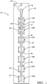
- Figure 1 illustrates an antenna device 20 that includes a substrate 22 and a transmission line 24 supported on the substrate 22.
- a plurality of conductive patches 26 are supported on the substrate 22.
- Each conductive patch 26 has a first end 28 coupled to the transmission line 24 and a second end 30 that is coupled to ground through conductive vias 32.
- the transmission line 24 comprises a differential twin line and the conductive patches 26 are arranged in sets including two of the conductive patches 26 facing each other on opposite sides of the transmission line 24.
- Each of the sets 26A-26G includes two of the conductive patches 26 facing each other along the length of the transmission line 24.
- the conductive patches 26 are resonators for emitting radiation.
- the illustrated example includes a radiation source 34, such as a substrate integrated waveguide or a microstrip line.
- This embodiment includes a transition 36, such as a balun, that couples the source of radiation 34 to the transmission line 24. The transition 36 balances an unbalanced signal from the source of radiation 34 before that signal propagates along the transmission line 24.
- each of the conductive patches has a first width W 1 at the first end 28 and a second width W 2 at the second end 30.
- the first width W 1 is smaller than the second width W 2 for each of the example conductive patches 26.
- the widths W 1 and W 2 are equal.
- the first width W 1 of at least one of the sets of patches 26 is different than the first width W 1 of at least one other of the sets of conductive patches 26.
- this example embodiment includes a different first width W 1 for each of the sets of conductive patches 26.
- the first width W 1 becomes progressively larger as the sets 26A-26G are spaced further from the source of radiation 34.
- the differing first widths W 1 provide different resonating powers for the difference sets of conductive patches.
- the sets of conductive patches 26C, 26D, 26E, 26F, and 26G have progressively larger first widths W 1 to provide for a tapered radiated power along the antenna device 20.
- Each of the conductive patches 26 includes a distance D between the first end 28 and the second end 30.
- the distance D determines or controls an operating frequency of the antenna device.
- a length L between the second ends 30 of each set of conductive patches 26 corresponds to approximately a one-half wavelength in the substrate of the radiation radiated by the conductive patches 26.
- Other conductive patch shapes and arrangements are possible and those skilled in the art who have the benefit of this description will understand how to configure a plurality of conductive patches having features like those of the example conductive patches to achieve the desired antenna performance that will meet their particular needs.
- the conductive vias 32 couple the second end 30 of the conductive patches 26 to a grounding layer 40 on an opposite side of the substrate 22 compared to the side of the substrate 22 on which the conductive patches 26 are supported.
- Figure 4 illustrates an example embodiment that includes a conductive layer 42 on the same side of the substrate 22 as the conductive patches 26.
- the conductive layer 42 includes a plurality of parasitic conductive elements 44 supported on the substrate 22.
- the parasitic conductive elements 44 are arranged along the substrate 22 so that the conductive layer 42 extends along the entire length of the transmission line 24.
- the parasitic conductive elements 44 operate to suppress ripples that otherwise would be associated with the radiation from the conductive patches 26.
- the conductive layer 42 which is established by the conductive parasitic elements 44, radiates out signal energy from the substrate to avoid such energy being further propagated along the substrate in a way that it would otherwise cause interference with other antennas.
- the conductive parasitic elements 44 effectively eliminate energy radiating through the substrate 22, which reduces or avoids ripples and interference among multiple antennas situated near each other.
- the parasitic elements 44 each include a respective conductive via 46 that couples the parasitic element 44 to the ground layer 40.
- Figure 5 illustrates how the conductive vias 46 are situated within or along the respective, coupled parasitic conductive elements 44.
- a conductive parasitic element 44A is closer to a conductive patch 26G than conductive parasitic elements 44B, 44C, and 44D.
- the position of the respective conductive vias 46 varies depending on the distance between the conductive patches 26 and the corresponding parasitic conductive element 44.
- the conductive via 46A associated with the conductive parasitic element 44A is closer to one edge 50A than an opposite edge 52A of that conductive parasitic element 44A. As the conductive parasitic elements 44 are situated progressively further from the conductive patches 26, the corresponding vias 46 are situated closer to a center of the coupled parasitic conductive element 44. In this example, the conductive via 46D is approximately centered between the edges 50D and 52D of the conductive parasitic element 44D.
- the different conductive via positions relative to the coupled parasitic conductive elements 44 addresses the fact that power decays moving along the substrate 22 in a direction away from the conductive patches 26.
- the conductive parasitic element 44D experiences a lower radiation power compared to the conductive parasitic elements 44A and 44B, which have their respective conductive vias 46A and 46B closer to the edge 50 that is facing toward the conductive patch 26G.
- Figure 6 illustrates another example embodiment in which the conductive layer 42 is a continuous layer of a conductive material supported on the same side of the substrate 22 as the conductive patches 26.
- the radiating power of the antenna device 20 is controllable by selecting the widths W 1 and W 2 of the conductive patches 26. Using different widths along the transmission line 24 allows for controlling the power distribution along the antenna device 20. Including a conductive layer 42 reduces or avoids ripple effects. With any of the example embodiments, it becomes possible to achieve wider operation bandwidth and radiation beamwidth while using relatively thin substrate layers, which provides a cost-effective and efficient antenna.
Abstract
Description
- Increasing amounts of technology are included on automotive vehicles. Radar and lidar sensing devices provide the capability to detect objects in a vicinity or pathway of the vehicle. Many such devices include a radiating antenna that emits the radiation used for object detection.
- While different antenna types have proven useful, they are not without shortcomings or drawbacks. For example, some antennas that are useful for short or medium range detection have the capability of covering a wide field of view, but experience high loss when the electromagnetic wave radiated from the antenna passes through the fascia of the vehicle. Such high losses are typically associated with vertical polarization of the antenna. One attempt to address that problem is to incorporate horizontal polarization. The difficulty associated with horizontal polarization, however, is that the impedance bandwidth is typically too narrow to satisfy production requirements. One approach to increase the impedance bandwidth includes increasing the thickness of the antenna substrate material. A disadvantage associated with that approach is that it increases cost.
- Another difficulty associated with some known radar antenna configurations is the occurrence of high frequency ripples resulting from radiation scattering from nearby antennas, electronic components on the vehicle, and other metal or dielectric materials in close proximity to the antennas. A further complication is that the ripples in the radiation pattern for each antenna occur at different angles and that affects the uniformity of the radiation patterns of all the antennas used for radar. A non-uniform radiation pattern significantly lowers the angle finding accuracy of the radar system.
- An illustrative example antenna device includes a substrate, a transmission line supported on the substrate, and a plurality of conductive patches supported on the substrate. Each conductive patch has a first end coupled to the transmission line and a second end coupled to ground. The plurality of conductive patches are arranged in sets including two of the conductive patches facing each other on opposite sides of the transmission line.
- In an example embodiment having one or more features of the antenna device of the previous paragraph, the conductive patches respectively have a distance between the first end and the second end, and an operating frequency of the antenna device is based on the distance.
- In an example embodiment having one or more features of the antenna device of any of the previous paragraphs, the conductive patches respectively have a first width near the first end and a radiating power of the conductive patches, respectively, is based on the width.
- In an example embodiment having one or more features of the antenna device of any of the previous paragraphs, the conductive patches respectively have a second width near the second end and the second width is different than the first width.
- In an example embodiment having one or more features of the antenna device of any of the previous paragraphs, the first width of two of the conductive patches is different than the first width of two others of the conductive patches.
- In an example embodiment having one or more features of the antenna device of any of the previous paragraphs, the two of the conductive patches are closer to a first end of the transmission line; the two others of the conductive patches are closer to a second, opposite end of the transmission line; and the first end of the transmission line is coupled to a source of radiation.
- In an example embodiment having one or more features of the antenna device of any of the previous paragraphs, a radiating power of the conductive patches, respectively, is based on the second width.
- In an example embodiment having one or more features of the antenna device of any of the previous paragraphs, the conductive patches are situated on one side of the substrate, the substrate includes a grounding layer spaced from the one side of the substrate, and the conductive patches respectively include a plurality of conductive vias coupled to the grounding layer.
- In an example embodiment having one or more features of the antenna device of any of the previous paragraphs, a length between the second ends of the conductive patches in each set corresponds to a one-half wavelength in the substrate of radiation radiated by the conductive patches.
- An example embodiment having one or more features of the antenna device of any of the previous paragraphs includes a conductive layer near the conductive patches and a plurality of conductive vias coupled between the conductive layer and ground. The conductive layer may comprise a continuous layer of conductive material
- In an example embodiment having one or more features of the antenna device of any of the previous paragraphs, the conductive layer comprises a plurality of parasitic conductive elements and each of the parasitic conductive elements is coupled with one of the conductive vias.
- In an example embodiment having one or more features of the antenna device of any of the previous paragraphs, each conductive via is situated in a position relative to edges of a coupled one of the parasitic conductive elements and the position of some of the vias is different than the position of others of the vias.
- In an example embodiment having one or more features of the antenna device of any of the previous paragraphs, the parasitic conductive elements coupled to the some of the vias are closer to the conductive patches than the parasitic conductive elements coupled to the others of the vias, and the respective position of the others of the vias is closer to a center of the respective coupled parasitic conductive elements than the position of the some of the vias.
- In an example embodiment having one or more features of the antenna device of any of the previous paragraphs, the conductive layer is coupled to the second ends of the conductive patches and the conductive layer has a dimension parallel to the transmission line that is at least as long as the transmission line.
- In an example embodiment having one or more features of the antenna device of any of the previous paragraphs, the conductive patches are on one surface of the substrate and the conductive layer is on the one surface of the substrate.
- In an example embodiment having one or more features of the antenna device of any of the previous paragraphs, the transmission line comprises a differential twin line.
- An example embodiment having one or more features of the antenna device of any of the previous paragraphs includes a source of radiation that provides an unbalanced signal and a transition coupling the source of radiation to the transmission line. The transition balances the unbalanced signal before the signal propagates along the transmission line.
- In an example embodiment having one or more features of the antenna device of any of the previous paragraphs, the source of radiation comprises a substrate integrated waveguide and the transition comprises a balun.
- In an example embodiment having one or more features of the antenna device of any of the previous paragraphs, the conductive patches each have a geometric configuration and the geometric configuration of the two conductive patches in each set is the same.
- Various features and advantages of at least one disclosed example embodiment will become apparent to those skilled in the art from the following detailed description. The drawings that accompany the detailed description can be briefly describe as follows.
-
-
Figure 1 schematically illustrates an example antenna designed according to an embodiment of this invention. -
Figure 2 illustrates selected features of the embodiment ofFigure 1 . -
Figure 3 is a cross-sectional illustration taken along the lines 3-3 inFigure 2 . -
Figure 4 schematically illustrates another example antenna configuration designed according to an embodiment of this invention. -
Figure 5 is a cross-sectional illustration taken along the lines 5-5 inFigure 4 . -
Figure 6 schematically illustrates another example antenna configuration designed according to an embodiment of this invention. - Embodiments of this invention provide an antenna including a transmission line and a plurality of conductive patches coupled with the transmission line. With embodiments of this invention, it is possible to achieve wider operation bandwidth and wider radiation beamwidth in a cost-effective manner while avoiding undesirable ripple effects.
-
Figure 1 illustrates anantenna device 20 that includes asubstrate 22 and atransmission line 24 supported on thesubstrate 22. A plurality ofconductive patches 26 are supported on thesubstrate 22. Eachconductive patch 26 has afirst end 28 coupled to thetransmission line 24 and asecond end 30 that is coupled to ground throughconductive vias 32. - In the illustrated example, the
transmission line 24 comprises a differential twin line and theconductive patches 26 are arranged in sets including two of theconductive patches 26 facing each other on opposite sides of thetransmission line 24. Each of thesets 26A-26G includes two of theconductive patches 26 facing each other along the length of thetransmission line 24. Theconductive patches 26 are resonators for emitting radiation. The illustrated example includes aradiation source 34, such as a substrate integrated waveguide or a microstrip line. This embodiment includes atransition 36, such as a balun, that couples the source ofradiation 34 to thetransmission line 24. Thetransition 36 balances an unbalanced signal from the source ofradiation 34 before that signal propagates along thetransmission line 24. - As shown in
Figure 2 , each of the conductive patches has a first width W1 at thefirst end 28 and a second width W2 at thesecond end 30. The first width W1 is smaller than the second width W2 for each of the exampleconductive patches 26. In other embodiments the widths W1 and W2 are equal. In the embodiment ofFigure 1 , the first width W1 of at least one of the sets ofpatches 26 is different than the first width W1 of at least one other of the sets ofconductive patches 26. As illustrated inFigure 1 , this example embodiment includes a different first width W1 for each of the sets ofconductive patches 26. In this example, the first width W1 becomes progressively larger as thesets 26A-26G are spaced further from the source ofradiation 34. - The differing first widths W1 provide different resonating powers for the difference sets of conductive patches. The sets of
conductive patches antenna device 20. - Each of the
conductive patches 26 includes a distance D between thefirst end 28 and thesecond end 30. The distance D determines or controls an operating frequency of the antenna device. Those skilled in the art who have the benefit of this description will be able to select an appropriate distance D to achieve an operating frequency that meets their particular needs. - A length L between the second ends 30 of each set of
conductive patches 26 corresponds to approximately a one-half wavelength in the substrate of the radiation radiated by theconductive patches 26. - The particular shape and arrangement of the
conductive patches 26, in the illustrated example, achieves desired antenna performance for a radar detection system that is useful on an automotive vehicle for example. Other conductive patch shapes and arrangements are possible and those skilled in the art who have the benefit of this description will understand how to configure a plurality of conductive patches having features like those of the example conductive patches to achieve the desired antenna performance that will meet their particular needs. - As shown in
Figure 3 , theconductive vias 32 couple thesecond end 30 of theconductive patches 26 to agrounding layer 40 on an opposite side of thesubstrate 22 compared to the side of thesubstrate 22 on which theconductive patches 26 are supported. -
Figure 4 illustrates an example embodiment that includes aconductive layer 42 on the same side of thesubstrate 22 as theconductive patches 26. In this example, theconductive layer 42 includes a plurality of parasiticconductive elements 44 supported on thesubstrate 22. The parasiticconductive elements 44 are arranged along thesubstrate 22 so that theconductive layer 42 extends along the entire length of thetransmission line 24. The parasiticconductive elements 44 operate to suppress ripples that otherwise would be associated with the radiation from theconductive patches 26. - The
conductive layer 42, which is established by the conductiveparasitic elements 44, radiates out signal energy from the substrate to avoid such energy being further propagated along the substrate in a way that it would otherwise cause interference with other antennas. The conductiveparasitic elements 44 effectively eliminate energy radiating through thesubstrate 22, which reduces or avoids ripples and interference among multiple antennas situated near each other. - The
parasitic elements 44 each include a respective conductive via 46 that couples theparasitic element 44 to theground layer 40.Figure 5 illustrates how theconductive vias 46 are situated within or along the respective, coupled parasiticconductive elements 44. As can be appreciated fromFigures 4 and5 , a conductiveparasitic element 44A is closer to aconductive patch 26G than conductiveparasitic elements conductive vias 46 varies depending on the distance between theconductive patches 26 and the corresponding parasiticconductive element 44. - The conductive via 46A associated with the conductive
parasitic element 44A is closer to oneedge 50A than anopposite edge 52A of that conductiveparasitic element 44A. As the conductiveparasitic elements 44 are situated progressively further from theconductive patches 26, the correspondingvias 46 are situated closer to a center of the coupled parasiticconductive element 44. In this example, the conductive via 46D is approximately centered between theedges parasitic element 44D. The different conductive via positions relative to the coupled parasiticconductive elements 44 addresses the fact that power decays moving along thesubstrate 22 in a direction away from theconductive patches 26. In the example ofFigure 5 , the conductiveparasitic element 44D experiences a lower radiation power compared to the conductiveparasitic elements conductive vias conductive patch 26G. -
Figure 6 illustrates another example embodiment in which theconductive layer 42 is a continuous layer of a conductive material supported on the same side of thesubstrate 22 as theconductive patches 26. - With any of the example embodiments, the radiating power of the
antenna device 20 is controllable by selecting the widths W1 and W2 of theconductive patches 26. Using different widths along thetransmission line 24 allows for controlling the power distribution along theantenna device 20. Including aconductive layer 42 reduces or avoids ripple effects. With any of the example embodiments, it becomes possible to achieve wider operation bandwidth and radiation beamwidth while using relatively thin substrate layers, which provides a cost-effective and efficient antenna. - While different embodiments are shown with features that appear distinct, such features are not limited to the particular embodiments disclosed above. Other combinations of such features are possible to realize other embodiments.
- The preceding description is illustrative rather than limiting in nature. Variations and modifications to the disclosed example embodiments may become apparent to those skilled in the art without departing from the essence of this invention.
Claims (15)
- An antenna device (20), comprising:a substrate (22);a transmission line (24) supported on the substrate (22);a plurality of conductive patches (26) supported on the substrate (22), each conductive patch having a first end (28) coupled to the transmission line (24) and a second end (30) coupled to ground, the plurality of conductive patches (26) being arranged in sets including two of the conductive patches (26) facing each other on opposite sides of the transmission line (24).
- The antenna device (20) of claim 1, wherein
the conductive patches (26) respectively have a distance between the first end (28) and the second end (30); and
an operating frequency of the antenna device (20) is based on the distance. - The antenna device (20) according to any one of the preceding claims, wherein
the conductive patches (26) respectively have a first width near the first end (28); and
a radiating power of the conductive patches (26), respectively, is based at least in part on the first width. - The antenna device (20) of claim 3, wherein
the conductive patches (26) respectively have a second width near the second end (30); and
the second width is different than the first width. - The antenna device (20) according to any one of the claims 3 and 4, wherein the first width of two of the conductive patches (26) is different than the first width of two others of the conductive patches (26).
- The antenna device (20) of claim 5, wherein
the two of the conductive patches (26) are closer to a first end (28) of the transmission line (24);
the two others of the conductive patches (26) are closer to a second, opposite end of the transmission line (24); and
the first end (28) of the transmission line (24) is coupled to a source of radiation (34). - The antenna device (20) according to any one of the preceding claims, wherein
the conductive patches (26) are situated on one side of the substrate (22);
the substrate (22) includes a grounding layer (40) spaced from the one side of the substrate (22); and
the conductive patches (26) respectively include a plurality of conductive vias (46) coupled to the grounding layer (40). - The antenna device (20) according to any one of the preceding claims, comprising
a conductive layer (42) near the conductive patches (26); and
a plurality of conductive vias (46) coupled between the conductive layer (42) and ground. - The antenna device (20) of claim 8, wherein
the conductive layer (42) comprises a plurality of parasitic conductive elements (44); and
each of the parasitic conductive elements (44) is coupled with one of the conductive vias (46). - The antenna device (20) of claim 9, wherein
each conductive via is situated in a position relative to edges of a coupled one of the parasitic conductive elements (44); and
the position of some of the vias is different than the position of others of the vias. - The antenna device (20) of claim 10, wherein
the parasitic conductive elements (44) coupled to the some of the vias are closer to the conductive patches (26) than the parasitic conductive elements (44) coupled to the others of the vias; and
the respective position of the others of the vias is closer to a center of the respective coupled parasitic conductive elements (44) than the position of the some of the vias. - The antenna device (20) according to any one of the claims 8 to 11, wherein
the conductive layer (42) is coupled to the second end (30)s of the conductive patches (26); and
the conductive layer (42) has a dimension parallel to the transmission line (24) that is at least as long as the transmission line (24). - The antenna device (20) of claim 8, wherein
the conductive patches (26) are on one surface of the substrate (22); and
the conductive layer (42) is on the one surface of the substrate (22). - The antenna device (20) according to any one of the preceding claims, comprising
a source of radiation (34) that provides an unbalanced signal; and
a transition (36) coupling the source of radiation to the transmission line (24), the transition (36) balancing the unbalanced signal before the signal propagates along the transmission line (24). - The antenna device (20) according to any one of the preceding claim, wherein
the conductive patches (26) each have a geometric configuration; and
the geometric configuration of the two conductive patches (26) in each set is the same.
Applications Claiming Priority (2)
| Application Number | Priority Date | Filing Date | Title |
|---|---|---|---|
| US201862626961P | 2018-02-06 | 2018-02-06 | |
| US16/219,248 US11217904B2 (en) | 2018-02-06 | 2018-12-13 | Wide angle coverage antenna with parasitic elements |
Publications (2)
| Publication Number | Publication Date |
|---|---|
| EP3522297A1 true EP3522297A1 (en) | 2019-08-07 |
| EP3522297B1 EP3522297B1 (en) | 2020-12-23 |
Family
ID=65138864
Family Applications (1)
| Application Number | Title | Priority Date | Filing Date |
|---|---|---|---|
| EP19152734.0A Active EP3522297B1 (en) | 2018-02-06 | 2019-01-21 | Wide angle coverage antenna |
Country Status (2)
| Country | Link |
|---|---|
| US (1) | US11217904B2 (en) |
| EP (1) | EP3522297B1 (en) |
Cited By (1)
| Publication number | Priority date | Publication date | Assignee | Title |
|---|---|---|---|---|
| CN113140881A (en) * | 2021-04-07 | 2021-07-20 | 博微太赫兹信息科技有限公司 | 45-degree-rotation-angle millimeter wave differential line-to-SIW (substrate integrated waveguide) structure |
Families Citing this family (13)
| Publication number | Priority date | Publication date | Assignee | Title |
|---|---|---|---|---|
| US10897088B2 (en) * | 2016-04-21 | 2021-01-19 | Veoneer Sweden Ab | Leaky-wave slotted microstrip antenna |
| US11424548B2 (en) * | 2018-05-01 | 2022-08-23 | Metawave Corporation | Method and apparatus for a meta-structure antenna array |
| TWI705614B (en) * | 2019-05-09 | 2020-09-21 | 和碩聯合科技股份有限公司 | Antenna structure |
| US11444377B2 (en) | 2019-10-03 | 2022-09-13 | Aptiv Technologies Limited | Radiation pattern reconfigurable antenna |
| US11502420B2 (en) | 2020-12-18 | 2022-11-15 | Aptiv Technologies Limited | Twin line fed dipole array antenna |
| US11901601B2 (en) | 2020-12-18 | 2024-02-13 | Aptiv Technologies Limited | Waveguide with a zigzag for suppressing grating lobes |
| US11749883B2 (en) | 2020-12-18 | 2023-09-05 | Aptiv Technologies Limited | Waveguide with radiation slots and parasitic elements for asymmetrical coverage |
| US11681015B2 (en) | 2020-12-18 | 2023-06-20 | Aptiv Technologies Limited | Waveguide with squint alteration |
| US11444364B2 (en) | 2020-12-22 | 2022-09-13 | Aptiv Technologies Limited | Folded waveguide for antenna |
| TWI752780B (en) * | 2020-12-31 | 2022-01-11 | 啓碁科技股份有限公司 | Antenna structure with wide beamwidth |
| US11668787B2 (en) | 2021-01-29 | 2023-06-06 | Aptiv Technologies Limited | Waveguide with lobe suppression |
| US11721905B2 (en) | 2021-03-16 | 2023-08-08 | Aptiv Technologies Limited | Waveguide with a beam-forming feature with radiation slots |
| US11616282B2 (en) | 2021-08-03 | 2023-03-28 | Aptiv Technologies Limited | Transition between a single-ended port and differential ports having stubs that match with input impedances of the single-ended and differential ports |
Citations (2)
| Publication number | Priority date | Publication date | Assignee | Title |
|---|---|---|---|---|
| DE2824053A1 (en) * | 1977-05-31 | 1978-12-14 | Emi Ltd | ANTENNA ARRANGEMENT |
| EP3096402A1 (en) * | 2015-05-20 | 2016-11-23 | Panasonic Intellectual Property Management Co., Ltd. | Antenna device, wireless communication apparatus, and radar apparatus |
Family Cites Families (14)
| Publication number | Priority date | Publication date | Assignee | Title |
|---|---|---|---|---|
| GB1294024A (en) | 1970-04-28 | 1972-10-25 | Emi Ltd | Improvements relating to aerial arrangements |
| EP0565754B1 (en) | 1992-04-15 | 1995-12-27 | Holger Blum | Stabilized coating composition on the basis of urethaneprepolymers having free isocyanate groups |
| US6262495B1 (en) | 1998-03-30 | 2001-07-17 | The Regents Of The University Of California | Circuit and method for eliminating surface currents on metals |
| JP2000332523A (en) | 1999-05-24 | 2000-11-30 | Hitachi Ltd | Radio tag, and its manufacture and arrangement |
| US20070004363A1 (en) * | 2003-05-12 | 2007-01-04 | Takuya Kusaka | Radio lan antenna |
| CN1964135A (en) | 2005-11-11 | 2007-05-16 | 启碁科技股份有限公司 | Channel hole and multi-inverse-F coupled wideband antenna and electronic device using same |
| TW200835057A (en) * | 2007-02-15 | 2008-08-16 | Advanced Connectek Inc | Integrated antenna |
| US20100134376A1 (en) * | 2008-12-01 | 2010-06-03 | Toyota Motor Engineering & Manufacturing North America, Inc. | Wideband rf 3d transitions |
| DE102010040793A1 (en) * | 2010-09-15 | 2012-03-15 | Robert Bosch Gmbh | Group antenna for radar sensors |
| KR101269711B1 (en) * | 2011-05-23 | 2013-05-30 | 주식회사 에이스테크놀로지 | Radar Array Antenna Using Open Stub |
| US10122074B2 (en) * | 2014-11-19 | 2018-11-06 | Panasonic Intellectual Property Management Co., Ltd. | Antenna device using EBG structure, wireless communication device, and radar device |
| JP6017003B1 (en) | 2015-10-06 | 2016-10-26 | 株式会社フジクラ | Microstrip antenna and manufacturing method thereof |
| EP3199976B1 (en) * | 2016-01-29 | 2022-04-20 | Denso Corporation | Planar radar antenna for automotive multi-mode and multi-target detection |
| CN107492705B (en) | 2017-08-18 | 2019-07-30 | 中国科学院电子学研究所 | Folded dipole antenna |
-
2018
- 2018-12-13 US US16/219,248 patent/US11217904B2/en active Active
-
2019
- 2019-01-21 EP EP19152734.0A patent/EP3522297B1/en active Active
Patent Citations (2)
| Publication number | Priority date | Publication date | Assignee | Title |
|---|---|---|---|---|
| DE2824053A1 (en) * | 1977-05-31 | 1978-12-14 | Emi Ltd | ANTENNA ARRANGEMENT |
| EP3096402A1 (en) * | 2015-05-20 | 2016-11-23 | Panasonic Intellectual Property Management Co., Ltd. | Antenna device, wireless communication apparatus, and radar apparatus |
Non-Patent Citations (1)
| Title |
|---|
| YUANXIN LI ET AL: "The Periodic Half-Width Microstrip Leaky-Wave Antenna With a Backward to Forward Scanning Capability", IEEE TRANSACTIONS ON ANTENNAS AND PROPAGATION, IEEE SERVICE CENTER, PISCATAWAY, NJ, US, vol. 57, no. 3, 3 March 2010 (2010-03-03), pages 963 - 966, XP011298722, ISSN: 0018-926X * |
Cited By (2)
| Publication number | Priority date | Publication date | Assignee | Title |
|---|---|---|---|---|
| CN113140881A (en) * | 2021-04-07 | 2021-07-20 | 博微太赫兹信息科技有限公司 | 45-degree-rotation-angle millimeter wave differential line-to-SIW (substrate integrated waveguide) structure |
| CN113140881B (en) * | 2021-04-07 | 2021-12-10 | 博微太赫兹信息科技有限公司 | 45-degree-rotation-angle millimeter wave differential line-to-SIW (substrate integrated waveguide) structure |
Also Published As
| Publication number | Publication date |
|---|---|
| US20190245276A1 (en) | 2019-08-08 |
| US11217904B2 (en) | 2022-01-04 |
| EP3522297B1 (en) | 2020-12-23 |
Similar Documents
| Publication | Publication Date | Title |
|---|---|---|
| EP3522297A1 (en) | Wide angle coverage antenna | |
| US11374333B2 (en) | Slot array antenna including parasitic features | |
| US10122074B2 (en) | Antenna device using EBG structure, wireless communication device, and radar device | |
| US20130300624A1 (en) | Broadband end-fire multi-layer antenna | |
| JP2016220029A (en) | Antenna device, radio communication device and radar device | |
| WO2014142202A1 (en) | Antenna device having patch antenna | |
| US20180145420A1 (en) | Wideband antenna radiating element and method for producing wideband antenna radiating element | |
| US10020594B2 (en) | Array antenna | |
| US11041938B2 (en) | Radar apparatus | |
| US20130027259A1 (en) | Traveling Wave Excitation Antenna And Planar Antenna | |
| US20080266195A1 (en) | Waveguide Slot Array Antenna Assembly | |
| KR20150059392A (en) | Microstripline-fed slot array antenna and manufacturing method thereof | |
| US8736514B2 (en) | Antenna | |
| US11411319B2 (en) | Antenna apparatus | |
| EP2963729A1 (en) | Stacked waveguide substrate, radio communication module, and radar system | |
| CN109428150A (en) | Antenna element, trailer-mounted radar and automobile | |
| CN109428175B (en) | Antenna unit, vehicle-mounted radar, and automobile | |
| KR101865135B1 (en) | Array Antenna | |
| KR101679553B1 (en) | Traveling-wave antenna with improved beam tilt deviation | |
| CN110120582B (en) | Antenna device | |
| CN109428176A (en) | Antenna element, trailer-mounted radar and automobile | |
| US9692138B2 (en) | Antenna device | |
| CN109428165A (en) | Antenna element, trailer-mounted radar and automobile | |
| WO2020246210A1 (en) | Antenna element | |
| US20220131278A1 (en) | Broadband planar array antenna |
Legal Events
| Date | Code | Title | Description |
|---|---|---|---|
| PUAI | Public reference made under article 153(3) epc to a published international application that has entered the european phase |
Free format text: ORIGINAL CODE: 0009012 |
|
| STAA | Information on the status of an ep patent application or granted ep patent |
Free format text: STATUS: THE APPLICATION HAS BEEN PUBLISHED |
|
| AK | Designated contracting states |
Kind code of ref document: A1 Designated state(s): AL AT BE BG CH CY CZ DE DK EE ES FI FR GB GR HR HU IE IS IT LI LT LU LV MC MK MT NL NO PL PT RO RS SE SI SK SM TR |
|
| AX | Request for extension of the european patent |
Extension state: BA ME |
|
| STAA | Information on the status of an ep patent application or granted ep patent |
Free format text: STATUS: REQUEST FOR EXAMINATION WAS MADE |
|
| 17P | Request for examination filed |
Effective date: 20200206 |
|
| RBV | Designated contracting states (corrected) |
Designated state(s): AL AT BE BG CH CY CZ DE DK EE ES FI FR GB GR HR HU IE IS IT LI LT LU LV MC MK MT NL NO PL PT RO RS SE SI SK SM TR |
|
| GRAP | Despatch of communication of intention to grant a patent |
Free format text: ORIGINAL CODE: EPIDOSNIGR1 |
|
| STAA | Information on the status of an ep patent application or granted ep patent |
Free format text: STATUS: GRANT OF PATENT IS INTENDED |
|
| INTG | Intention to grant announced |
Effective date: 20200710 |
|
| GRAS | Grant fee paid |
Free format text: ORIGINAL CODE: EPIDOSNIGR3 |
|
| GRAA | (expected) grant |
Free format text: ORIGINAL CODE: 0009210 |
|
| STAA | Information on the status of an ep patent application or granted ep patent |
Free format text: STATUS: THE PATENT HAS BEEN GRANTED |
|
| AK | Designated contracting states |
Kind code of ref document: B1 Designated state(s): AL AT BE BG CH CY CZ DE DK EE ES FI FR GB GR HR HU IE IS IT LI LT LU LV MC MK MT NL NO PL PT RO RS SE SI SK SM TR |
|
| REG | Reference to a national code |
Ref country code: GB Ref legal event code: FG4D |
|
| REG | Reference to a national code |
Ref country code: DE Ref legal event code: R096 Ref document number: 602019001796 Country of ref document: DE |
|
| REG | Reference to a national code |
Ref country code: AT Ref legal event code: REF Ref document number: 1348618 Country of ref document: AT Kind code of ref document: T Effective date: 20210115 |
|
| REG | Reference to a national code |
Ref country code: IE Ref legal event code: FG4D |
|
| PG25 | Lapsed in a contracting state [announced via postgrant information from national office to epo] |
Ref country code: GR Free format text: LAPSE BECAUSE OF FAILURE TO SUBMIT A TRANSLATION OF THE DESCRIPTION OR TO PAY THE FEE WITHIN THE PRESCRIBED TIME-LIMIT Effective date: 20210324 Ref country code: NO Free format text: LAPSE BECAUSE OF FAILURE TO SUBMIT A TRANSLATION OF THE DESCRIPTION OR TO PAY THE FEE WITHIN THE PRESCRIBED TIME-LIMIT Effective date: 20210323 Ref country code: RS Free format text: LAPSE BECAUSE OF FAILURE TO SUBMIT A TRANSLATION OF THE DESCRIPTION OR TO PAY THE FEE WITHIN THE PRESCRIBED TIME-LIMIT Effective date: 20201223 Ref country code: FI Free format text: LAPSE BECAUSE OF FAILURE TO SUBMIT A TRANSLATION OF THE DESCRIPTION OR TO PAY THE FEE WITHIN THE PRESCRIBED TIME-LIMIT Effective date: 20201223 |
|
| REG | Reference to a national code |
Ref country code: AT Ref legal event code: MK05 Ref document number: 1348618 Country of ref document: AT Kind code of ref document: T Effective date: 20201223 |
|
| REG | Reference to a national code |
Ref country code: NL Ref legal event code: MP Effective date: 20201223 |
|
| PG25 | Lapsed in a contracting state [announced via postgrant information from national office to epo] |
Ref country code: BG Free format text: LAPSE BECAUSE OF FAILURE TO SUBMIT A TRANSLATION OF THE DESCRIPTION OR TO PAY THE FEE WITHIN THE PRESCRIBED TIME-LIMIT Effective date: 20210323 Ref country code: LV Free format text: LAPSE BECAUSE OF FAILURE TO SUBMIT A TRANSLATION OF THE DESCRIPTION OR TO PAY THE FEE WITHIN THE PRESCRIBED TIME-LIMIT Effective date: 20201223 Ref country code: SE Free format text: LAPSE BECAUSE OF FAILURE TO SUBMIT A TRANSLATION OF THE DESCRIPTION OR TO PAY THE FEE WITHIN THE PRESCRIBED TIME-LIMIT Effective date: 20201223 |
|
| PG25 | Lapsed in a contracting state [announced via postgrant information from national office to epo] |
Ref country code: NL Free format text: LAPSE BECAUSE OF FAILURE TO SUBMIT A TRANSLATION OF THE DESCRIPTION OR TO PAY THE FEE WITHIN THE PRESCRIBED TIME-LIMIT Effective date: 20201223 Ref country code: HR Free format text: LAPSE BECAUSE OF FAILURE TO SUBMIT A TRANSLATION OF THE DESCRIPTION OR TO PAY THE FEE WITHIN THE PRESCRIBED TIME-LIMIT Effective date: 20201223 |
|
| REG | Reference to a national code |
Ref country code: LT Ref legal event code: MG9D |
|
| PG25 | Lapsed in a contracting state [announced via postgrant information from national office to epo] |
Ref country code: LT Free format text: LAPSE BECAUSE OF FAILURE TO SUBMIT A TRANSLATION OF THE DESCRIPTION OR TO PAY THE FEE WITHIN THE PRESCRIBED TIME-LIMIT Effective date: 20201223 Ref country code: RO Free format text: LAPSE BECAUSE OF FAILURE TO SUBMIT A TRANSLATION OF THE DESCRIPTION OR TO PAY THE FEE WITHIN THE PRESCRIBED TIME-LIMIT Effective date: 20201223 Ref country code: PT Free format text: LAPSE BECAUSE OF FAILURE TO SUBMIT A TRANSLATION OF THE DESCRIPTION OR TO PAY THE FEE WITHIN THE PRESCRIBED TIME-LIMIT Effective date: 20210423 Ref country code: SM Free format text: LAPSE BECAUSE OF FAILURE TO SUBMIT A TRANSLATION OF THE DESCRIPTION OR TO PAY THE FEE WITHIN THE PRESCRIBED TIME-LIMIT Effective date: 20201223 Ref country code: SK Free format text: LAPSE BECAUSE OF FAILURE TO SUBMIT A TRANSLATION OF THE DESCRIPTION OR TO PAY THE FEE WITHIN THE PRESCRIBED TIME-LIMIT Effective date: 20201223 Ref country code: CZ Free format text: LAPSE BECAUSE OF FAILURE TO SUBMIT A TRANSLATION OF THE DESCRIPTION OR TO PAY THE FEE WITHIN THE PRESCRIBED TIME-LIMIT Effective date: 20201223 Ref country code: EE Free format text: LAPSE BECAUSE OF FAILURE TO SUBMIT A TRANSLATION OF THE DESCRIPTION OR TO PAY THE FEE WITHIN THE PRESCRIBED TIME-LIMIT Effective date: 20201223 |
|
| PG25 | Lapsed in a contracting state [announced via postgrant information from national office to epo] |
Ref country code: AT Free format text: LAPSE BECAUSE OF FAILURE TO SUBMIT A TRANSLATION OF THE DESCRIPTION OR TO PAY THE FEE WITHIN THE PRESCRIBED TIME-LIMIT Effective date: 20201223 Ref country code: PL Free format text: LAPSE BECAUSE OF FAILURE TO SUBMIT A TRANSLATION OF THE DESCRIPTION OR TO PAY THE FEE WITHIN THE PRESCRIBED TIME-LIMIT Effective date: 20201223 |
|
| REG | Reference to a national code |
Ref country code: DE Ref legal event code: R097 Ref document number: 602019001796 Country of ref document: DE |
|
| PG25 | Lapsed in a contracting state [announced via postgrant information from national office to epo] |
Ref country code: IS Free format text: LAPSE BECAUSE OF FAILURE TO SUBMIT A TRANSLATION OF THE DESCRIPTION OR TO PAY THE FEE WITHIN THE PRESCRIBED TIME-LIMIT Effective date: 20210423 Ref country code: MC Free format text: LAPSE BECAUSE OF FAILURE TO SUBMIT A TRANSLATION OF THE DESCRIPTION OR TO PAY THE FEE WITHIN THE PRESCRIBED TIME-LIMIT Effective date: 20201223 Ref country code: LU Free format text: LAPSE BECAUSE OF NON-PAYMENT OF DUE FEES Effective date: 20210121 |
|
| REG | Reference to a national code |
Ref country code: BE Ref legal event code: MM Effective date: 20210131 |
|
| PG25 | Lapsed in a contracting state [announced via postgrant information from national office to epo] |
Ref country code: AL Free format text: LAPSE BECAUSE OF FAILURE TO SUBMIT A TRANSLATION OF THE DESCRIPTION OR TO PAY THE FEE WITHIN THE PRESCRIBED TIME-LIMIT Effective date: 20201223 Ref country code: IT Free format text: LAPSE BECAUSE OF FAILURE TO SUBMIT A TRANSLATION OF THE DESCRIPTION OR TO PAY THE FEE WITHIN THE PRESCRIBED TIME-LIMIT Effective date: 20201223 |
|
| PLBE | No opposition filed within time limit |
Free format text: ORIGINAL CODE: 0009261 |
|
| STAA | Information on the status of an ep patent application or granted ep patent |
Free format text: STATUS: NO OPPOSITION FILED WITHIN TIME LIMIT |
|
| PG25 | Lapsed in a contracting state [announced via postgrant information from national office to epo] |
Ref country code: DK Free format text: LAPSE BECAUSE OF FAILURE TO SUBMIT A TRANSLATION OF THE DESCRIPTION OR TO PAY THE FEE WITHIN THE PRESCRIBED TIME-LIMIT Effective date: 20201223 |
|
| 26N | No opposition filed |
Effective date: 20210924 |
|
| PG25 | Lapsed in a contracting state [announced via postgrant information from national office to epo] |
Ref country code: ES Free format text: LAPSE BECAUSE OF FAILURE TO SUBMIT A TRANSLATION OF THE DESCRIPTION OR TO PAY THE FEE WITHIN THE PRESCRIBED TIME-LIMIT Effective date: 20201223 Ref country code: IE Free format text: LAPSE BECAUSE OF NON-PAYMENT OF DUE FEES Effective date: 20210121 |
|
| PG25 | Lapsed in a contracting state [announced via postgrant information from national office to epo] |
Ref country code: SI Free format text: LAPSE BECAUSE OF FAILURE TO SUBMIT A TRANSLATION OF THE DESCRIPTION OR TO PAY THE FEE WITHIN THE PRESCRIBED TIME-LIMIT Effective date: 20201223 |
|
| PG25 | Lapsed in a contracting state [announced via postgrant information from national office to epo] |
Ref country code: IS Free format text: LAPSE BECAUSE OF FAILURE TO SUBMIT A TRANSLATION OF THE DESCRIPTION OR TO PAY THE FEE WITHIN THE PRESCRIBED TIME-LIMIT Effective date: 20210423 |
|
| PG25 | Lapsed in a contracting state [announced via postgrant information from national office to epo] |
Ref country code: BE Free format text: LAPSE BECAUSE OF NON-PAYMENT OF DUE FEES Effective date: 20210131 |
|
| REG | Reference to a national code |
Ref country code: CH Ref legal event code: PL |
|
| PG25 | Lapsed in a contracting state [announced via postgrant information from national office to epo] |
Ref country code: LI Free format text: LAPSE BECAUSE OF NON-PAYMENT OF DUE FEES Effective date: 20220131 Ref country code: CH Free format text: LAPSE BECAUSE OF NON-PAYMENT OF DUE FEES Effective date: 20220131 |
|
| PGFP | Annual fee paid to national office [announced via postgrant information from national office to epo] |
Ref country code: FR Payment date: 20230123 Year of fee payment: 5 |
|
| PGFP | Annual fee paid to national office [announced via postgrant information from national office to epo] |
Ref country code: GB Payment date: 20230117 Year of fee payment: 5 Ref country code: DE Payment date: 20230106 Year of fee payment: 5 |
|
| P01 | Opt-out of the competence of the unified patent court (upc) registered |
Effective date: 20230424 |
|
| PG25 | Lapsed in a contracting state [announced via postgrant information from national office to epo] |
Ref country code: CY Free format text: LAPSE BECAUSE OF FAILURE TO SUBMIT A TRANSLATION OF THE DESCRIPTION OR TO PAY THE FEE WITHIN THE PRESCRIBED TIME-LIMIT Effective date: 20201223 |
|
| PG25 | Lapsed in a contracting state [announced via postgrant information from national office to epo] |
Ref country code: HU Free format text: LAPSE BECAUSE OF FAILURE TO SUBMIT A TRANSLATION OF THE DESCRIPTION OR TO PAY THE FEE WITHIN THE PRESCRIBED TIME-LIMIT; INVALID AB INITIO Effective date: 20190121 |