EP3521095A1 - Battery-charger device for electric vehicles - Google Patents
Battery-charger device for electric vehicles Download PDFInfo
- Publication number
- EP3521095A1 EP3521095A1 EP19154153.1A EP19154153A EP3521095A1 EP 3521095 A1 EP3521095 A1 EP 3521095A1 EP 19154153 A EP19154153 A EP 19154153A EP 3521095 A1 EP3521095 A1 EP 3521095A1
- Authority
- EP
- European Patent Office
- Prior art keywords
- battery
- current
- electrically connected
- stage
- charger device
- Prior art date
- Legal status (The legal status is an assumption and is not a legal conclusion. Google has not performed a legal analysis and makes no representation as to the accuracy of the status listed.)
- Granted
Links
- 238000001914 filtration Methods 0.000 claims abstract description 28
- 238000006243 chemical reaction Methods 0.000 claims abstract description 27
- 239000003990 capacitor Substances 0.000 claims description 5
- 230000000295 complement effect Effects 0.000 claims description 4
- 238000004519 manufacturing process Methods 0.000 description 3
- 230000002860 competitive effect Effects 0.000 description 2
- 230000005611 electricity Effects 0.000 description 2
- 230000008030 elimination Effects 0.000 description 2
- 238000003379 elimination reaction Methods 0.000 description 2
- 230000004044 response Effects 0.000 description 2
- 230000005355 Hall effect Effects 0.000 description 1
- 230000002238 attenuated effect Effects 0.000 description 1
- 230000001419 dependent effect Effects 0.000 description 1
- 238000010586 diagram Methods 0.000 description 1
- 238000000034 method Methods 0.000 description 1
- 230000007935 neutral effect Effects 0.000 description 1
Images


Classifications
-
- B—PERFORMING OPERATIONS; TRANSPORTING
- B60—VEHICLES IN GENERAL
- B60L—PROPULSION OF ELECTRICALLY-PROPELLED VEHICLES; SUPPLYING ELECTRIC POWER FOR AUXILIARY EQUIPMENT OF ELECTRICALLY-PROPELLED VEHICLES; ELECTRODYNAMIC BRAKE SYSTEMS FOR VEHICLES IN GENERAL; MAGNETIC SUSPENSION OR LEVITATION FOR VEHICLES; MONITORING OPERATING VARIABLES OF ELECTRICALLY-PROPELLED VEHICLES; ELECTRIC SAFETY DEVICES FOR ELECTRICALLY-PROPELLED VEHICLES
- B60L3/00—Electric devices on electrically-propelled vehicles for safety purposes; Monitoring operating variables, e.g. speed, deceleration or energy consumption
- B60L3/0023—Detecting, eliminating, remedying or compensating for drive train abnormalities, e.g. failures within the drive train
- B60L3/003—Detecting, eliminating, remedying or compensating for drive train abnormalities, e.g. failures within the drive train relating to inverters
-
- B—PERFORMING OPERATIONS; TRANSPORTING
- B60—VEHICLES IN GENERAL
- B60L—PROPULSION OF ELECTRICALLY-PROPELLED VEHICLES; SUPPLYING ELECTRIC POWER FOR AUXILIARY EQUIPMENT OF ELECTRICALLY-PROPELLED VEHICLES; ELECTRODYNAMIC BRAKE SYSTEMS FOR VEHICLES IN GENERAL; MAGNETIC SUSPENSION OR LEVITATION FOR VEHICLES; MONITORING OPERATING VARIABLES OF ELECTRICALLY-PROPELLED VEHICLES; ELECTRIC SAFETY DEVICES FOR ELECTRICALLY-PROPELLED VEHICLES
- B60L15/00—Methods, circuits, or devices for controlling the traction-motor speed of electrically-propelled vehicles
- B60L15/02—Methods, circuits, or devices for controlling the traction-motor speed of electrically-propelled vehicles characterised by the form of the current used in the control circuit
-
- B—PERFORMING OPERATIONS; TRANSPORTING
- B60—VEHICLES IN GENERAL
- B60L—PROPULSION OF ELECTRICALLY-PROPELLED VEHICLES; SUPPLYING ELECTRIC POWER FOR AUXILIARY EQUIPMENT OF ELECTRICALLY-PROPELLED VEHICLES; ELECTRODYNAMIC BRAKE SYSTEMS FOR VEHICLES IN GENERAL; MAGNETIC SUSPENSION OR LEVITATION FOR VEHICLES; MONITORING OPERATING VARIABLES OF ELECTRICALLY-PROPELLED VEHICLES; ELECTRIC SAFETY DEVICES FOR ELECTRICALLY-PROPELLED VEHICLES
- B60L53/00—Methods of charging batteries, specially adapted for electric vehicles; Charging stations or on-board charging equipment therefor; Exchange of energy storage elements in electric vehicles
- B60L53/30—Constructional details of charging stations
-
- B—PERFORMING OPERATIONS; TRANSPORTING
- B60—VEHICLES IN GENERAL
- B60L—PROPULSION OF ELECTRICALLY-PROPELLED VEHICLES; SUPPLYING ELECTRIC POWER FOR AUXILIARY EQUIPMENT OF ELECTRICALLY-PROPELLED VEHICLES; ELECTRODYNAMIC BRAKE SYSTEMS FOR VEHICLES IN GENERAL; MAGNETIC SUSPENSION OR LEVITATION FOR VEHICLES; MONITORING OPERATING VARIABLES OF ELECTRICALLY-PROPELLED VEHICLES; ELECTRIC SAFETY DEVICES FOR ELECTRICALLY-PROPELLED VEHICLES
- B60L53/00—Methods of charging batteries, specially adapted for electric vehicles; Charging stations or on-board charging equipment therefor; Exchange of energy storage elements in electric vehicles
- B60L53/60—Monitoring or controlling charging stations
- B60L53/62—Monitoring or controlling charging stations in response to charging parameters, e.g. current, voltage or electrical charge
-
- H—ELECTRICITY
- H02—GENERATION; CONVERSION OR DISTRIBUTION OF ELECTRIC POWER
- H02M—APPARATUS FOR CONVERSION BETWEEN AC AND AC, BETWEEN AC AND DC, OR BETWEEN DC AND DC, AND FOR USE WITH MAINS OR SIMILAR POWER SUPPLY SYSTEMS; CONVERSION OF DC OR AC INPUT POWER INTO SURGE OUTPUT POWER; CONTROL OR REGULATION THEREOF
- H02M1/00—Details of apparatus for conversion
- H02M1/14—Arrangements for reducing ripples from dc input or output
- H02M1/15—Arrangements for reducing ripples from dc input or output using active elements
-
- H—ELECTRICITY
- H02—GENERATION; CONVERSION OR DISTRIBUTION OF ELECTRIC POWER
- H02M—APPARATUS FOR CONVERSION BETWEEN AC AND AC, BETWEEN AC AND DC, OR BETWEEN DC AND DC, AND FOR USE WITH MAINS OR SIMILAR POWER SUPPLY SYSTEMS; CONVERSION OF DC OR AC INPUT POWER INTO SURGE OUTPUT POWER; CONTROL OR REGULATION THEREOF
- H02M3/00—Conversion of dc power input into dc power output
- H02M3/02—Conversion of dc power input into dc power output without intermediate conversion into ac
- H02M3/04—Conversion of dc power input into dc power output without intermediate conversion into ac by static converters
- H02M3/10—Conversion of dc power input into dc power output without intermediate conversion into ac by static converters using discharge tubes with control electrode or semiconductor devices with control electrode
- H02M3/145—Conversion of dc power input into dc power output without intermediate conversion into ac by static converters using discharge tubes with control electrode or semiconductor devices with control electrode using devices of a triode or transistor type requiring continuous application of a control signal
- H02M3/155—Conversion of dc power input into dc power output without intermediate conversion into ac by static converters using discharge tubes with control electrode or semiconductor devices with control electrode using devices of a triode or transistor type requiring continuous application of a control signal using semiconductor devices only
- H02M3/156—Conversion of dc power input into dc power output without intermediate conversion into ac by static converters using discharge tubes with control electrode or semiconductor devices with control electrode using devices of a triode or transistor type requiring continuous application of a control signal using semiconductor devices only with automatic control of output voltage or current, e.g. switching regulators
- H02M3/158—Conversion of dc power input into dc power output without intermediate conversion into ac by static converters using discharge tubes with control electrode or semiconductor devices with control electrode using devices of a triode or transistor type requiring continuous application of a control signal using semiconductor devices only with automatic control of output voltage or current, e.g. switching regulators including plural semiconductor devices as final control devices for a single load
- H02M3/1582—Buck-boost converters
-
- H—ELECTRICITY
- H02—GENERATION; CONVERSION OR DISTRIBUTION OF ELECTRIC POWER
- H02M—APPARATUS FOR CONVERSION BETWEEN AC AND AC, BETWEEN AC AND DC, OR BETWEEN DC AND DC, AND FOR USE WITH MAINS OR SIMILAR POWER SUPPLY SYSTEMS; CONVERSION OF DC OR AC INPUT POWER INTO SURGE OUTPUT POWER; CONTROL OR REGULATION THEREOF
- H02M3/00—Conversion of dc power input into dc power output
- H02M3/02—Conversion of dc power input into dc power output without intermediate conversion into ac
- H02M3/04—Conversion of dc power input into dc power output without intermediate conversion into ac by static converters
- H02M3/10—Conversion of dc power input into dc power output without intermediate conversion into ac by static converters using discharge tubes with control electrode or semiconductor devices with control electrode
- H02M3/145—Conversion of dc power input into dc power output without intermediate conversion into ac by static converters using discharge tubes with control electrode or semiconductor devices with control electrode using devices of a triode or transistor type requiring continuous application of a control signal
- H02M3/155—Conversion of dc power input into dc power output without intermediate conversion into ac by static converters using discharge tubes with control electrode or semiconductor devices with control electrode using devices of a triode or transistor type requiring continuous application of a control signal using semiconductor devices only
- H02M3/156—Conversion of dc power input into dc power output without intermediate conversion into ac by static converters using discharge tubes with control electrode or semiconductor devices with control electrode using devices of a triode or transistor type requiring continuous application of a control signal using semiconductor devices only with automatic control of output voltage or current, e.g. switching regulators
- H02M3/158—Conversion of dc power input into dc power output without intermediate conversion into ac by static converters using discharge tubes with control electrode or semiconductor devices with control electrode using devices of a triode or transistor type requiring continuous application of a control signal using semiconductor devices only with automatic control of output voltage or current, e.g. switching regulators including plural semiconductor devices as final control devices for a single load
- H02M3/1584—Conversion of dc power input into dc power output without intermediate conversion into ac by static converters using discharge tubes with control electrode or semiconductor devices with control electrode using devices of a triode or transistor type requiring continuous application of a control signal using semiconductor devices only with automatic control of output voltage or current, e.g. switching regulators including plural semiconductor devices as final control devices for a single load with a plurality of power processing stages connected in parallel
-
- B—PERFORMING OPERATIONS; TRANSPORTING
- B60—VEHICLES IN GENERAL
- B60L—PROPULSION OF ELECTRICALLY-PROPELLED VEHICLES; SUPPLYING ELECTRIC POWER FOR AUXILIARY EQUIPMENT OF ELECTRICALLY-PROPELLED VEHICLES; ELECTRODYNAMIC BRAKE SYSTEMS FOR VEHICLES IN GENERAL; MAGNETIC SUSPENSION OR LEVITATION FOR VEHICLES; MONITORING OPERATING VARIABLES OF ELECTRICALLY-PROPELLED VEHICLES; ELECTRIC SAFETY DEVICES FOR ELECTRICALLY-PROPELLED VEHICLES
- B60L2210/00—Converter types
- B60L2210/10—DC to DC converters
-
- B—PERFORMING OPERATIONS; TRANSPORTING
- B60—VEHICLES IN GENERAL
- B60L—PROPULSION OF ELECTRICALLY-PROPELLED VEHICLES; SUPPLYING ELECTRIC POWER FOR AUXILIARY EQUIPMENT OF ELECTRICALLY-PROPELLED VEHICLES; ELECTRODYNAMIC BRAKE SYSTEMS FOR VEHICLES IN GENERAL; MAGNETIC SUSPENSION OR LEVITATION FOR VEHICLES; MONITORING OPERATING VARIABLES OF ELECTRICALLY-PROPELLED VEHICLES; ELECTRIC SAFETY DEVICES FOR ELECTRICALLY-PROPELLED VEHICLES
- B60L2240/00—Control parameters of input or output; Target parameters
- B60L2240/40—Drive Train control parameters
- B60L2240/52—Drive Train control parameters related to converters
- B60L2240/529—Current
-
- H—ELECTRICITY
- H02—GENERATION; CONVERSION OR DISTRIBUTION OF ELECTRIC POWER
- H02M—APPARATUS FOR CONVERSION BETWEEN AC AND AC, BETWEEN AC AND DC, OR BETWEEN DC AND DC, AND FOR USE WITH MAINS OR SIMILAR POWER SUPPLY SYSTEMS; CONVERSION OF DC OR AC INPUT POWER INTO SURGE OUTPUT POWER; CONTROL OR REGULATION THEREOF
- H02M3/00—Conversion of dc power input into dc power output
- H02M3/02—Conversion of dc power input into dc power output without intermediate conversion into ac
- H02M3/04—Conversion of dc power input into dc power output without intermediate conversion into ac by static converters
- H02M3/10—Conversion of dc power input into dc power output without intermediate conversion into ac by static converters using discharge tubes with control electrode or semiconductor devices with control electrode
- H02M3/145—Conversion of dc power input into dc power output without intermediate conversion into ac by static converters using discharge tubes with control electrode or semiconductor devices with control electrode using devices of a triode or transistor type requiring continuous application of a control signal
- H02M3/155—Conversion of dc power input into dc power output without intermediate conversion into ac by static converters using discharge tubes with control electrode or semiconductor devices with control electrode using devices of a triode or transistor type requiring continuous application of a control signal using semiconductor devices only
- H02M3/156—Conversion of dc power input into dc power output without intermediate conversion into ac by static converters using discharge tubes with control electrode or semiconductor devices with control electrode using devices of a triode or transistor type requiring continuous application of a control signal using semiconductor devices only with automatic control of output voltage or current, e.g. switching regulators
-
- Y—GENERAL TAGGING OF NEW TECHNOLOGICAL DEVELOPMENTS; GENERAL TAGGING OF CROSS-SECTIONAL TECHNOLOGIES SPANNING OVER SEVERAL SECTIONS OF THE IPC; TECHNICAL SUBJECTS COVERED BY FORMER USPC CROSS-REFERENCE ART COLLECTIONS [XRACs] AND DIGESTS
- Y02—TECHNOLOGIES OR APPLICATIONS FOR MITIGATION OR ADAPTATION AGAINST CLIMATE CHANGE
- Y02T—CLIMATE CHANGE MITIGATION TECHNOLOGIES RELATED TO TRANSPORTATION
- Y02T10/00—Road transport of goods or passengers
- Y02T10/60—Other road transportation technologies with climate change mitigation effect
- Y02T10/64—Electric machine technologies in electromobility
Definitions
- the present invention relates to a battery-charger device for electric vehicles.
- a charging station for electric vehicles is normally equipped with a multiplicity of battery-charger devices, each of which is electrically connectable to the mains electricity supply and to the battery of an electric vehicle.
- Battery-charger devices comprising a diode rectification stage and a DC/DC conversion stage electrically connected in cascade.
- battery-charger devices of the type indicated above have several drawbacks.
- the presence of an input diode rectification stage leads to the generation of a ripple component in the current supplied to the battery by the DC/DC conversion stage, which can take on a significant amplitude (for example several dozen A), which is generally unacceptable for using with a battery-charger device.
- the primary aim of the present invention is to provide a battery-charger device for electric vehicles that makes it possible to overcome the aforementioned problems of the known art.
- an object of the present invention is to provide a battery-charger device in which the ripple component of the current supplied to the battery has a greatly reduced or negligible amplitude.
- Another object of the present invention is to provide a battery-charger device that has a very compact structure and a very small size.
- Yet another object of the present invention is to provide a battery-charger device that is easy to manufacture at an industrial level, at competitive costs.
- the battery-charger device comprises input terminals electrically connectable to a source of alternating electric current (AC) and output terminals electrically connectable to a battery or other equivalent device for accumulating electrical energy, which can be charged in direct current conditions (DC).
- AC alternating electric current
- DC direct current conditions
- the battery-charger device comprises a rectification stage electrically connected to said input terminals.
- the aforementioned rectification stage is adapted to receive a first voltage and a first current in AC and to outfeed a second voltage and a second current in DC.
- the battery-charger device further comprises a DC/DC conversion stage electrically connected between the rectification stage and the output terminals, therefore in a cascade with said rectification stage.
- This conversion stage is adapted to infeed said second voltage and said second current and to outfeed, for the battery, a third voltage and a third current.
- the aforementioned third current, outfed from the DC/DC conversion stage has a DC component and an AC component (ripple component) overlapping one another.
- the battery-charger device comprises an active filtering stage electrically connected to the output terminals, in parallel with respect to the aforementioned DC/DC conversion stage.
- This active filtering stage is adapted to outfeed, for the battery, a fourth AC current having a wave form such as to attenuate or eliminate the AC component of the third current outfed, for the battery, from the DC/DC conversion stage.
- the fourth current, outfed from the active filtering stage has a module corresponding to and opposite phase from the module and phase of the AC component of the third current outfed from the DC/DC conversion stage.
- the battery-charger device comprises sensor means adapted to provide detecting signals indicating the currents supplied to the electric load.
- the active filtering stage of the battery-charger device is adapted to receive the aforementioned detecting signals and to outfeed said fourth current based on these detecting signals.
- the battery-charger device comprises a low-pass passive filtering stage electrically connected to the input terminals in parallel with respect to the rectification stage.
- the active filtering stage comprises an electronic switching circuit comprising a first and second transistor and a control unit adapted to provide control signals for controlling the operational state of said first and second transistor.
- this control unit is adapted to receive the detecting signals provided by the sensor means and to provide said control signals based on these detecting signals.
- this control unit runs a control program for performing a duty-cycle (PWM) for the first and second transistor of the electronic switching circuit.
- PWM duty-cycle
- the present invention also relates to a charging station for electric vehicles, comprising at least one battery-charger device, according to the present invention.
- the present invention relates to a battery-charger device 1 for low-voltage applications.
- low-voltage refers to operating voltages below 1 kV AC and 1.5 kV DC.
- the battery-charger device 1 performs an AC/DC type power conversion between an electric power source PW operating in alternating current (AC) conditions, e.g. the mains electricity supply, and a battery B, in particular a battery for electric vehicles or another equivalent device for accumulating electrical energy, for example a capacitor bank.
- AC alternating current
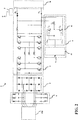
- the battery-charger device 1 comprises at least one pair of input terminals IN 1 , IN 2 electrically connectable to the electric power source PW.
- the battery-charger device 1 comprises one pair of input terminals for each electric phase of the electric power source PW.
- the power source PW is a multi-phase type, for example three-phase.
- the battery-charger device 1 comprises multiple (e.g. three) pairs of input terminals, as illustrated in the embodiment shown in Figure 2 .
- the battery-charger device 1 comprises one pair of output terminals O 1 , O 2 electrically connectable to the battery B operating in direct current (DC) conditions.
- the battery-charger device 1 comprises a rectification stage 2 electrically connected to the input terminals IN 1 , IN 2 .
- the rectification stage 2 is adapted to receive a first voltage V 1 and a first current I 1 (single-phase or multi-phase) in AC and to outfeed a second voltage V 2 and a second current I 2 in DC.
- the rectification stage 2 is a diode bridge with 4*N or 6*N impulses, where N is the number of electrical phases of the electric power source PW.
- N is the number of electrical phases of the electric power source PW.
- the rectification stage 2 is a diode bridge with 12 or 18 impulses.
- the rectification stage 2 is of a known type and therefore, for obvious purposes of brevity, it will only be described here as it relates to significant aspects of the invention.
- the battery-charger device 1 comprises a DC/DC conversion stage 3 electrically connected between the rectification stage 2 and the output terminals O 1 , O 2 .
- the conversion stage 3 is adapted to infeed the second voltage V 2 and the second current I 2 from the rectification stage 2 and to outfeed, to the electric charge B, a third voltage V 3 and a third current I 3 .
- Figure 5 shows the path of the current I 3 supplied to battery B by the conversion stage 3.
- the current I 3 comprises a DC component I DC and an AC component (ripple component) I R overlapping one another.
- the AC component I R has relatively low frequencies (e.g. 300, 600 Hz for three-phase applications or 100Hz for single-phase applications).
- the conversion stage 3 is a DC/DC converter in a buck-boost configuration. This solution makes it possible to offer a wide range of output values for the output voltage V 3 provided to the battery B.
- the conversion stage 3 is of a known type and therefore, for obvious purposes of brevity, it will only be described here as it relates to significant aspects of the invention.
- the battery-charger device 1 comprises a low-pass passive filtering stage 6 electrically connected to the input terminals IN 1 , IN 2 in parallel with respect to the rectification stage 2.
- the passive filtering stage 6 is an LC-type filtering stage comprising an LC-series circuit electrically connected between each of the input terminals IN 1 , IN 2 and a neutral node, for example earth.
- the passive filtering stage 6 is of a known type and therefore, for obvious purposes of brevity, it will only be described here as it relates to significant aspects of the invention.
- the battery-charger device 1 comprises an active filtering stage 4 electrically connected to the output terminals O 1 , O 2 in parallel with respect to the conversion stage 3.
- the active filtering stage 4 is adapted to outfeed to the battery B, a fourth AC current I 4 having a wave form such as to attenuate or eliminate the AC component I R of the third current I 3 outfed from the conversion stage 3.
- the fourth current I 4 has a module corresponding to and opposite phase from the module and phase of the AC component I R of the third current I 3 outfed from the conversion stage 3.
- the AC component I R of the third current I 3 can be effectively attenuated to negligible values (or effectively eliminated) and the battery B can be fed only by the DC component I DC of the third current I 3 .
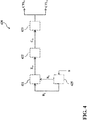
- the battery-charger device 1 comprises sensor means 5 adapted to provide detecting signals S indicating the currents (e.g. current I 3 ) provided to the battery B by the battery-charger device 1.
- sensor means 5 adapted to provide detecting signals S indicating the currents (e.g. current I 3 ) provided to the battery B by the battery-charger device 1.
- the sensor means 5 may comprise one or more shunt resistance circuits or Hall-effect sensors.
- the senor means 5 are of a known type and therefore, for obvious purposes of brevity, they will only be described here as they relate to significant aspects of the invention.
- the active filtering stage 4 is adapted to receive the detecting signals S provided by the sensor means 5 and to outfeed the fourth current I 4 based on these detecting signals.
- the active filtering stage 4 comprises an electronic switching circuit 41 and a control unit 42 adapted to provide control signals CTL 1 , CTL 2 for controlling the operational state of the electronic switching circuit 41.
- the electronic switching circuit 41 comprises an inductor L 2 having a first terminal L 21 electrically connected to a common electric node N and a second terminal L 22 electrically connected to a first output terminal O 1 .
- the switching circuit 41 comprises one pair of transistors T 1 , T 2 having power terminals electrically connected to a common electric node N.
- the transistors T 1 , T 2 may be devices of a known type, for example BJT, MOSFET, IGBT, GTO or a similar type.
- the switching circuit 41 comprises:
- the switching circuit 41 comprises a capacitor C 2 having a terminal C 21 electrically connected to the first power terminal C T1 of the first transistor T 1 and to the second power terminal E T2 of the second transistor T 2 .
- control unit 42 can be either digital or analogue.
- control unit 42 comprises at least one digital data processing device, for example comprising a micro-processor.
- control unit 42 may be part of a control unit (not illustrated) intended to control operation of the conversion stage 3.
- control unit 42 runs a control program 420 adapted to run-time define the duty-cycle for the transistors T 1 , T 2 .
- control unit 42 carries out specific software instructions stored on a memory support for implementing the functional blocks of the control program 420.
- control program 420 comprises a comparator block 421 adapted to infeed reference signals R 1 , R 2 indicating the instantaneous values (I R + I DC ) and the average value (I DC ) of the third current I 3 provided to the battery B by the conversion stage 3.
- control unit 42 is adapted to receive the detecting signals S provided by the sensor means 5.
- the reference signals R 1 , R 2 may be advantageously provided by a processing block 425 of the control unit 42 adapted to receive and process the detecting signals S provided by the sensor means 5.
- control program 420 comprises a proportional integrator block 422 422 adapted to receive the error signal E rr and to outfeed a duty-cycle signal C D in response to the error signal E rr .
- control program 420 comprises a control block PWM 423 adapted to receive the duty-cycle signal C D and to outfeed the first and second control signal CTL 1 , CTL 2 configured so that the first and second transistors T 1 , T 2 assume operational states ON, OFF that are complementary to one another.
- control program 420 The operation of the control program 420 and the switching circuit 41 are now described in greater detail.
- the control block PWM 423 receives the duty-cycle signal C D calculated based on the error signal E rr . From figure 5 it is apparent that the duty-cycle signal C D , being calculated based on the error signal E rr , has a sinusoidal form, similar to currents I R and I 4 , but with a frequency double that of these currents.
- the control block PWM 423 compares the duty-cycle signal C D with a modulating signal P (triangular wave) having a frequency much greater (around 10 times greater) than the frequency of the duty-cycle signal C D . Based on this comparison, it outfeeds control signals CTL 1 , CTL 2 configured as impulsive signals complementary to one another.
- the transistors T 1 , T 2 Upon receipt of the control signals CTL 1 , CTL 2 , the transistors T 1 , T 2 assume operational states complementary to one another. Therefore, when the transistor T 1 is in a conducting state (ON), the transistor T 2 is in a non-conducting state (OFF), and vice-versa.
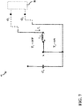
- Figure 6 shows the operation of the switching circuit 41 when the transistors T 1 , T 2 are in a conducting state (ON) and a non-conducting state (OFF) respectively.
- the current I L flowing along the inductor L 2 tends to increase given that the capacitor C 2 is electrically connected in parallel to the battery B.
- Figure 7 shows the operation of the switching circuit 41 when the transistors T 1 , T 2 are in a non-conducting state (OFF) and a conducting state (ON) respectively.
- the current I L flowing along the inductor L 2 tends to decrease given that the capacitor C 2 is electrically disconnected from the battery B.
- the active filtering stage included in the battery-charger device ensures an effective reduction or elimination of the AC component in the outfeed current provided to the battery. This makes it possible to power the latter by means of a DC current without the need to provide a costly and cumbersome filtering stage LC downstream of the rectification stage 2.
- the battery-charger device thus has a very compact structure that makes it particularly suitable for use in charging stations for electric vehicles.
- the battery-charger device, according to the present invention is characterised for its notable manufacturing simplicity. It can be easily produced industrially using known types of printed circuit manufacture.
- the battery-charger device according to the present invention, is therefore easily manufactured industrially at competitive costs with respect to similar devices currently available.
Abstract
Description
- The present invention relates to a battery-charger device for electric vehicles.
- As is known, a charging station for electric vehicles is normally equipped with a multiplicity of battery-charger devices, each of which is electrically connectable to the mains electricity supply and to the battery of an electric vehicle.
- Battery-charger devices are known comprising a diode rectification stage and a DC/DC conversion stage electrically connected in cascade.
- These devices are highly compact and small in size since the aforementioned rectification stage can easily be designed with smaller dimensions than a traditional input stage for a battery-charger device.
- Unfortunately, battery-charger devices of the type indicated above have several drawbacks. The presence of an input diode rectification stage leads to the generation of a ripple component in the current supplied to the battery by the DC/DC conversion stage, which can take on a significant amplitude (for example several dozen A), which is generally unacceptable for using with a battery-charger device.
- To reduce this ripple component, it is possible to provide an LC-type filtering stage between the rectification stage and the aforementioned conversion stage.
- Given that the aforementioned ripple component has relatively low frequencies (e.g. 300-600 Hz), this solution proves to be complex and costly to produce industrially. Indeed, the provision of a low-frequency LC filtering stage involves the use of inductors with relatively high inductance values.
- The primary aim of the present invention is to provide a battery-charger device for electric vehicles that makes it possible to overcome the aforementioned problems of the known art.
- In the context of this aim, an object of the present invention is to provide a battery-charger device in which the ripple component of the current supplied to the battery has a greatly reduced or negligible amplitude.
- Another object of the present invention is to provide a battery-charger device that has a very compact structure and a very small size.
- Yet another object of the present invention is to provide a battery-charger device that is easy to manufacture at an industrial level, at competitive costs.
- This aim and these objects, together with other objects that will become evident from the following description and accompanying drawings, are achieved, according to the present invention, by a battery-charger device, according to
claim 1 and the related dependent claims set out below. - In a general definition thereof, the battery-charger device, according to the present invention, comprises input terminals electrically connectable to a source of alternating electric current (AC) and output terminals electrically connectable to a battery or other equivalent device for accumulating electrical energy, which can be charged in direct current conditions (DC).
- The battery-charger device, according to the present invention, comprises a rectification stage electrically connected to said input terminals. The aforementioned rectification stage is adapted to receive a first voltage and a first current in AC and to outfeed a second voltage and a second current in DC.
- The battery-charger device, according to the present invention, further comprises a DC/DC conversion stage electrically connected between the rectification stage and the output terminals, therefore in a cascade with said rectification stage. This conversion stage is adapted to infeed said second voltage and said second current and to outfeed, for the battery, a third voltage and a third current. The aforementioned third current, outfed from the DC/DC conversion stage, has a DC component and an AC component (ripple component) overlapping one another.
- According to the present invention, the battery-charger device comprises an active filtering stage electrically connected to the output terminals, in parallel with respect to the aforementioned DC/DC conversion stage. This active filtering stage is adapted to outfeed, for the battery, a fourth AC current having a wave form such as to attenuate or eliminate the AC component of the third current outfed, for the battery, from the DC/DC conversion stage. Preferably, the fourth current, outfed from the active filtering stage, has a module corresponding to and opposite phase from the module and phase of the AC component of the third current outfed from the DC/DC conversion stage.
- Preferably, the battery-charger device, according to the present invention, comprises sensor means adapted to provide detecting signals indicating the currents supplied to the electric load. The active filtering stage of the battery-charger device is adapted to receive the aforementioned detecting signals and to outfeed said fourth current based on these detecting signals.
- Preferably, the battery-charger device, according to the present invention, comprises a low-pass passive filtering stage electrically connected to the input terminals in parallel with respect to the rectification stage.
- Preferably, the active filtering stage comprises an electronic switching circuit comprising a first and second transistor and a control unit adapted to provide control signals for controlling the operational state of said first and second transistor.
- Preferably, this control unit is adapted to receive the detecting signals provided by the sensor means and to provide said control signals based on these detecting signals.
- Preferably, this control unit runs a control program for performing a duty-cycle (PWM) for the first and second transistor of the electronic switching circuit.
- In a further aspect, the present invention also relates to a charging station for electric vehicles, comprising at least one battery-charger device, according to the present invention.
- Further characteristics and advantages of the battery-charger device, according to the present invention, will become more apparent from the following description thereof, illustrated by way of non-limiting example in the accompanying drawings, wherein:
-
Figure 1 shows a block diagram of the battery-charger device, according to the present invention; and -
Figures 2-3 shows a schematic view of the battery-charger device, according to the present invention, in a possible embodiment variant; and -
Figures 4-8 briefly describe the operation of the filtering stage in the embodiment variant of the battery-charger device, according to the present invention, shown infigures 2-3 . - With reference to the aforementioned figures, the present invention relates to a battery-
charger device 1 for low-voltage applications. - For the purpose of clarity, note that the term "low-voltage" refers to operating voltages below 1 kV AC and 1.5 kV DC.
- The battery-
charger device 1 performs an AC/DC type power conversion between an electric power source PW operating in alternating current (AC) conditions, e.g. the mains electricity supply, and a battery B, in particular a battery for electric vehicles or another equivalent device for accumulating electrical energy, for example a capacitor bank. - The battery-
charger device 1 comprises at least one pair of input terminals IN1, IN2 electrically connectable to the electric power source PW. - Advantageously, the battery-
charger device 1 comprises one pair of input terminals for each electric phase of the electric power source PW. - Preferably, the power source PW is a multi-phase type, for example three-phase. In this case, the battery-
charger device 1 comprises multiple (e.g. three) pairs of input terminals, as illustrated in the embodiment shown inFigure 2 . - The battery-
charger device 1 comprises one pair of output terminals O1, O2 electrically connectable to the battery B operating in direct current (DC) conditions. - The battery-
charger device 1 comprises a rectification stage 2 electrically connected to the input terminals IN1, IN2. - The rectification stage 2 is adapted to receive a first voltage V1 and a first current I1 (single-phase or multi-phase) in AC and to outfeed a second voltage V2 and a second current I2 in DC.
- Preferably, the rectification stage 2 is a diode bridge with 4*N or 6*N impulses, where N is the number of electrical phases of the electric power source PW. For example, in the case where the electric power source PW is a three-phase type, as shown in
figure 2 , the rectification stage 2 is a diode bridge with 12 or 18 impulses. - In general, however, the rectification stage 2 is of a known type and therefore, for obvious purposes of brevity, it will only be described here as it relates to significant aspects of the invention.
- The battery-
charger device 1 comprises a DC/DC conversion stage 3 electrically connected between the rectification stage 2 and the output terminals O1, O2. - The
conversion stage 3 is adapted to infeed the second voltage V2 and the second current I2 from the rectification stage 2 and to outfeed, to the electric charge B, a third voltage V3 and a third current I3. -
Figure 5 shows the path of the current I3 supplied to battery B by theconversion stage 3. As can be seen, the current I3 comprises a DC component IDC and an AC component (ripple component) IR overlapping one another. - In general, the AC component IR has relatively low frequencies (e.g. 300, 600 Hz for three-phase applications or 100Hz for single-phase applications).
- Preferably, the
conversion stage 3 is a DC/DC converter in a buck-boost configuration. This solution makes it possible to offer a wide range of output values for the output voltage V3 provided to the battery B. - In general, however, the
conversion stage 3 is of a known type and therefore, for obvious purposes of brevity, it will only be described here as it relates to significant aspects of the invention. - Preferably, the battery-
charger device 1 comprises a low-pass passive filtering stage 6 electrically connected to the input terminals IN1, IN2 in parallel with respect to the rectification stage 2. - Preferably, the passive filtering stage 6 is an LC-type filtering stage comprising an LC-series circuit electrically connected between each of the input terminals IN1, IN2 and a neutral node, for example earth.
- In general, however, the passive filtering stage 6 is of a known type and therefore, for obvious purposes of brevity, it will only be described here as it relates to significant aspects of the invention.
- According to the present invention, the battery-
charger device 1 comprises an active filtering stage 4 electrically connected to the output terminals O1, O2 in parallel with respect to theconversion stage 3. - The active filtering stage 4 is adapted to outfeed to the battery B, a fourth AC current I4 having a wave form such as to attenuate or eliminate the AC component IR of the third current I3 outfed from the
conversion stage 3. - Advantageously, as can be seen from
figure 4 , the fourth current I4 has a module corresponding to and opposite phase from the module and phase of the AC component IR of the third current I3 outfed from theconversion stage 3. - In practice, for the fourth current I4, outfed from the active filtering stage 4, the following relationship is valid: I4 = - IR.
- As can be seen from the above, it is evident that thanks to the active filtering stage 4, the AC component IR of the third current I3 can be effectively attenuated to negligible values (or effectively eliminated) and the battery B can be fed only by the DC component IDC of the third current I3.
- In practice, the current IB, provided to the electric charge B by the battery-
charger device 1, is given by the following equation: IB = I3 + I4 = IDC + IR- IR = IDC. - Preferably, the battery-
charger device 1 comprises sensor means 5 adapted to provide detecting signals S indicating the currents (e.g. current I3) provided to the battery B by the battery-charger device 1. - The sensor means 5 may comprise one or more shunt resistance circuits or Hall-effect sensors.
- In general, however, the sensor means 5 are of a known type and therefore, for obvious purposes of brevity, they will only be described here as they relate to significant aspects of the invention.
- Preferably, the active filtering stage 4 is adapted to receive the detecting signals S provided by the sensor means 5 and to outfeed the fourth current I4 based on these detecting signals. Preferably, the active filtering stage 4 comprises an
electronic switching circuit 41 and acontrol unit 42 adapted to provide control signals CTL1, CTL2 for controlling the operational state of theelectronic switching circuit 41. - Preferably, the
electronic switching circuit 41 comprises an inductor L2 having a first terminal L21 electrically connected to a common electric node N and a second terminal L22 electrically connected to a first output terminal O1. - Preferably, the switching
circuit 41 comprises one pair of transistors T1, T2 having power terminals electrically connected to a common electric node N. - The transistors T1, T2 may be devices of a known type, for example BJT, MOSFET, IGBT, GTO or a similar type.
- In particular, the switching
circuit 41 comprises: - a first transistor T1 having a first power terminal CT1 (for example the collector or drain terminal), a second power terminal ET1 (for example the emitter or source terminal) electrically connected to the common electric node N and to a control terminal GT1 (for example the base or gate terminal) electrically connected to the
control unit 42 so as to receive a first control signal CTL1 therefrom; - a second transistor T2 having a first power terminal CT2 (for example the collector or drain terminal) electrically connected to the common electric node N, a second power terminal ET2 (for example the emitter or source terminal) electrically connected to the second output terminal O2 and a control terminal GT2 (for example the base or gate terminal) electrically connected to the
control unit 42 so as to receive a second control signal CTL2 therefrom. - Preferably, the switching
circuit 41 comprises a capacitor C2 having a terminal C21 electrically connected to the first power terminal CT1 of the first transistor T1 and to the second power terminal ET2 of the second transistor T2. - In principle, the
control unit 42 can be either digital or analogue. - Preferably, the
control unit 42 comprises at least one digital data processing device, for example comprising a micro-processor. - According to some embodiment variants, the
control unit 42 may be part of a control unit (not illustrated) intended to control operation of theconversion stage 3. - Preferably, the
control unit 42 runs acontrol program 420 adapted to run-time define the duty-cycle for the transistors T1, T2. - Preferably, the
control unit 42 carries out specific software instructions stored on a memory support for implementing the functional blocks of thecontrol program 420. - Preferably, the
control program 420 comprises acomparator block 421 adapted to infeed reference signals R1, R2 indicating the instantaneous values (IR + IDC) and the average value (IDC) of the third current I3 provided to the battery B by theconversion stage 3. - Preferably, the
control unit 42 is adapted to receive the detecting signals S provided by the sensor means 5. In this case, as shown infigure 4 , the reference signals R1, R2 may be advantageously provided by aprocessing block 425 of thecontrol unit 42 adapted to receive and process the detecting signals S provided by the sensor means 5. - In response to the reference signals R1, R2, the
comparator block 421 outfeeds an error signal Err indicating the difference between the instantaneous value and the average value of the third current I3, in practice of the AC current I4 = -IR that needs to be added to the third current I3 (provided by the conversion stage 3) so that the battery B is powered by a DC current IB. - Preferably, the
control program 420 comprises aproportional integrator block 422 422 adapted to receive the error signal Err and to outfeed a duty-cycle signal CD in response to the error signal Err. - Preferably, the
control program 420 comprises acontrol block PWM 423 adapted to receive the duty-cycle signal CD and to outfeed the first and second control signal CTL1, CTL2 configured so that the first and second transistors T1, T2 assume operational states ON, OFF that are complementary to one another. - The operation of the
control program 420 and the switchingcircuit 41 are now described in greater detail. - The
control block PWM 423 receives the duty-cycle signal CD calculated based on the error signal Err. Fromfigure 5 it is apparent that the duty-cycle signal CD, being calculated based on the error signal Err, has a sinusoidal form, similar to currents IR and I4, but with a frequency double that of these currents. - The
control block PWM 423 compares the duty-cycle signal CD with a modulating signal P (triangular wave) having a frequency much greater (around 10 times greater) than the frequency of the duty-cycle signal CD. Based on this comparison, it outfeeds control signals CTL1, CTL2 configured as impulsive signals complementary to one another. - Upon receipt of the control signals CTL1, CTL2, the transistors T1, T2 assume operational states complementary to one another. Therefore, when the transistor T1 is in a conducting state (ON), the transistor T2 is in a non-conducting state (OFF), and vice-versa.
-
Figure 6 shows the operation of the switchingcircuit 41 when the transistors T1, T2 are in a conducting state (ON) and a non-conducting state (OFF) respectively. In this operational condition, the current IL flowing along the inductor L2 tends to increase given that the capacitor C2 is electrically connected in parallel to the battery B. -
Figure 7 shows the operation of the switchingcircuit 41 when the transistors T1, T2 are in a non-conducting state (OFF) and a conducting state (ON) respectively. In this operational condition, the current IL flowing along the inductor L2 tends to decrease given that the capacitor C2 is electrically disconnected from the battery B. - By suitably alternating the periods of conductivity and non-conductivity of the transistors T1, T2 (with much higher switching frequencies than the frequency of the duty-cycle signal CD) it is possible to modulate the current IL flowing in the inductor L2 so that it follows a desired wave form, in particular the desired wave form for the fourth current I4 so as to obtain adequate attenuation or elimination of the AC component IR of the third current I3, according to the relationship described above.
- It can be seen in practice how the battery-charger device, according to the present invention, achieves the pre-set objects.
- The active filtering stage included in the battery-charger device, according to the present invention, ensures an effective reduction or elimination of the AC component in the outfeed current provided to the battery. This makes it possible to power the latter by means of a DC current without the need to provide a costly and cumbersome filtering stage LC downstream of the rectification stage 2.
- The battery-charger device, according to the present invention, thus has a very compact structure that makes it particularly suitable for use in charging stations for electric vehicles. The battery-charger device, according to the present invention, is characterised for its notable manufacturing simplicity. It can be easily produced industrially using known types of printed circuit manufacture.
- The battery-charger device, according to the present invention, is therefore easily manufactured industrially at competitive costs with respect to similar devices currently available.
Claims (8)
- Battery-charger device for electric vehicles comprising:- input terminals (IN1, IN2) electrically connectable to an AC electric power source (PW);- output terminals (O1, O2) electrically connectable to a battery (B);- a rectification stage (2) electrically connected to said input terminals, said rectification stage being adapted to receive a first voltage (V1) and a first current (I1) in AC and to outfeed a second voltage (V2) and a second current (I2) in DC;- a DC/DC conversion stage (3) electrically connected between said rectification stage and said output terminals, said DC/DC conversion stage being adapted to infeed said second voltage (V2) and said second current (I2) and to outfeed, for said battery (B), a third voltage (V3) and a third current (I3), said third current (I3) having a DC component (IDC) and an AC component (IR);characterised in that it comprises an active filtering stage (4) electrically connected to said output terminals (O1, O2) in parallel with respect to said DC/DC conversion stage, said active filtering stage being adapted to outfeed, for said battery (B), a fourth AC current (I4) having a wave form such as to attenuate or eliminate the AC component (IR) of said third current (I3).
- Battery-charger device, according to claim 1, characterised in that said fourth current (I4) has a module corresponding to and opposite phase from the module and phase of the AC component (IR) of said third current (I3).
- Battery-charger device, according to one or more of the previous claims, characterised in that it comprises sensor means (5) adapted to provide detecting signals (S) indicating the currents (I3) provided to said battery (B), said active filtering stage being adapted to receive said detecting signals and to provide said fourth current (I4) based on said detecting signals.
- Battery-charger device, according to one or more of the previous claims, characterised in that it comprises a low-pass passive filtering stage (6) electrically connected to said input terminals (IN1, IN2), in parallel with respect to said rectification stage (2).
- Battery-charger device, according to one or more of the previous claims, characterised in that said active filtering stage (4) comprises un electronic switching circuit (41) comprising a first and second transistor (T1, T2) and a control unit (42) adapted to provide control signals (CTL1, CTL2) for controlling the operational state of said first and second transistor.
- Battery-charger device, according to claim 5, characterised in that said electronic switching circuit (41) comprises:- an inductor (L2) having a terminal (L21) electrically connected to a common electric node (N) and a terminal (L22) electrically connected to a first output terminal (O1);- said first transistor (T1) having a first power terminal (CT1), a second power terminal (ET1) electrically connected to said common electric node (N) and a control terminal (GT1) electrically connected to said control unit (42) so as to receive a first control signal (CTL1) from said control unit;- said second transistor (T2) having a first power terminal (CT2) electrically connected to said common electric node (N), a second power terminal (ET2) electrically connected to a second output terminal (O2) and a control terminal (GT2) electrically connected to said control unit (42) so as to receive a second control signal (CTL2) from said control unit;- a capacitor (C2) having a terminal (C21) electrically connected to the first power terminal (CT1) of said first transistor (T1) and a terminal electrically connected to the second power terminal (ET2) of said second transistor (T2).
- Battery-charger device, according to claim 6, characterised in that said control unit (42) runs a control program (420) comprising:- a comparator block (421) adapted to receive a first reference signal (R1) indicating the instantaneous value of said third current (I3) and a second reference signal (R2) indicating the average value of said third current (I3) and to provide an error signal (Err) indicating the difference between the instantaneous value and the average value of said third current;- a proportional integrator block (422) adapted to receive said error signal (Err) and to provide a duty-cycle signal (CD);- a control block PWM (423) adapted to receive said duty-cycle signal (CD) and to provide said control signals (CTL1, CTL2) for controlling the operational state of said first and second transistor (T1, T2), said control signals (CTL1, CTL2) being configured so that said first and second transistor (T1, T2) assume operational states (ON, OFF) that are complementary to one another.
- Charging station for electric vehicles, characterised in that it comprises at least one battery-charger device (1), according to one or more of the previous claims.
Applications Claiming Priority (1)
| Application Number | Priority Date | Filing Date | Title |
|---|---|---|---|
| IT202018000001793U IT201800001793U1 (en) | 2018-02-01 | 2018-02-01 | BATTERY CHARGER DEVICE FOR ELECTRIC VEHICLES. |
Publications (2)
| Publication Number | Publication Date |
|---|---|
| EP3521095A1 true EP3521095A1 (en) | 2019-08-07 |
| EP3521095B1 EP3521095B1 (en) | 2022-06-08 |
Family
ID=65440757
Family Applications (1)
| Application Number | Title | Priority Date | Filing Date |
|---|---|---|---|
| EP19154153.1A Active EP3521095B1 (en) | 2018-02-01 | 2019-01-29 | Battery-charger device for electric vehicles |
Country Status (2)
| Country | Link |
|---|---|
| EP (1) | EP3521095B1 (en) |
| IT (1) | IT201800001793U1 (en) |
Citations (4)
| Publication number | Priority date | Publication date | Assignee | Title |
|---|---|---|---|---|
| EP1833153A2 (en) * | 2006-03-07 | 2007-09-12 | United Technologies Corporation | Electric engine start system with active rectifier |
| US20140285139A1 (en) * | 2013-03-20 | 2014-09-25 | Samsung Electronics Co., Ltd. | Wireless power transmission and reception system |
| WO2016124681A1 (en) * | 2015-02-04 | 2016-08-11 | Eth Zurich | Control method and device for the active compensation of power supply- or load dependent fluctuations of the power flow of a power electronic converter system |
| US20160236580A1 (en) * | 2015-02-13 | 2016-08-18 | Mcmaster University | Dual voltage charging system with an integrated active filter auxiliary power module |
-
2018
- 2018-02-01 IT IT202018000001793U patent/IT201800001793U1/en unknown
-
2019
- 2019-01-29 EP EP19154153.1A patent/EP3521095B1/en active Active
Patent Citations (4)
| Publication number | Priority date | Publication date | Assignee | Title |
|---|---|---|---|---|
| EP1833153A2 (en) * | 2006-03-07 | 2007-09-12 | United Technologies Corporation | Electric engine start system with active rectifier |
| US20140285139A1 (en) * | 2013-03-20 | 2014-09-25 | Samsung Electronics Co., Ltd. | Wireless power transmission and reception system |
| WO2016124681A1 (en) * | 2015-02-04 | 2016-08-11 | Eth Zurich | Control method and device for the active compensation of power supply- or load dependent fluctuations of the power flow of a power electronic converter system |
| US20160236580A1 (en) * | 2015-02-13 | 2016-08-18 | Mcmaster University | Dual voltage charging system with an integrated active filter auxiliary power module |
Non-Patent Citations (1)
| Title |
|---|
| SHAHIN A ET AL: "New Method to Filter HF Current Ripples Generated by Current-Fed DC/DC Converters", IEEE TRANSACTIONS ON POWER ELECTRONICS, INSTITUTE OF ELECTRICAL AND ELECTRONICS ENGINEERS, USA, vol. 26, no. 12, 1 December 2011 (2011-12-01), pages 3832 - 3842, XP011479938, ISSN: 0885-8993, DOI: 10.1109/TPEL.2011.2134870 * |
Also Published As
| Publication number | Publication date |
|---|---|
| IT201800001793U1 (en) | 2019-08-01 |
| EP3521095B1 (en) | 2022-06-08 |
Similar Documents
| Publication | Publication Date | Title |
|---|---|---|
| US8116103B2 (en) | Device for feeding electric energy into a power grid and DC converter for such a device | |
| US8531854B2 (en) | Power factor correction converter and power factor correction conversion device | |
| US11557983B2 (en) | Coupled inductors inverter topology | |
| CN109478851B (en) | DC/DC converter | |
| US8385091B2 (en) | 3-phase high-power UPS | |
| US20140063884A1 (en) | Inverter device | |
| US20150008748A1 (en) | Power Converter Circuit, Power Supply System and Method | |
| US20090201706A1 (en) | Apparatus for feeding electrical energy into a power grid and DC voltage converter for such an apparatus | |
| US9252653B2 (en) | Power factor correction converter and control method thereof | |
| US10530274B2 (en) | Hybrid clocking method for single-phase transformer-free network inverters | |
| WO2014152948A2 (en) | Bidirectional power converter | |
| US10673320B2 (en) | Snubber circuit and power conversion system including same | |
| US8576598B2 (en) | Systems, methods, and apparatus for converting direct current (DC) power to alternating current (AC) power | |
| EP3700072B1 (en) | Ac-dc pfc converter for single-phase and three-phase operation | |
| US9680376B2 (en) | Power conversion electronics having conversion and inverter circuitry | |
| US10312825B2 (en) | Five-level half bridge inverter topology with high voltage utilization ratio | |
| US9431924B2 (en) | Power source inverter for use with a photovoltaic solar panel | |
| US20230249564A1 (en) | Charging device and vehicle | |
| KR20160013176A (en) | Converter assembly having multi-step converters connected in parallel and method for controlling said multi-step converters | |
| JP5362657B2 (en) | Power converter | |
| CN109075720B (en) | Power conversion device | |
| US20230223868A1 (en) | Power Converter | |
| EP3521095B1 (en) | Battery-charger device for electric vehicles | |
| CN215682129U (en) | Intelligent power module IPM and household appliance | |
| US20080238377A1 (en) | Device for transforming and stabilizing a primary ac voltage for supplying an electric load |
Legal Events
| Date | Code | Title | Description |
|---|---|---|---|
| PUAI | Public reference made under article 153(3) epc to a published international application that has entered the european phase |
Free format text: ORIGINAL CODE: 0009012 |
|
| STAA | Information on the status of an ep patent application or granted ep patent |
Free format text: STATUS: THE APPLICATION HAS BEEN PUBLISHED |
|
| AK | Designated contracting states |
Kind code of ref document: A1 Designated state(s): AL AT BE BG CH CY CZ DE DK EE ES FI FR GB GR HR HU IE IS IT LI LT LU LV MC MK MT NL NO PL PT RO RS SE SI SK SM TR |
|
| AX | Request for extension of the european patent |
Extension state: BA ME |
|
| RIN1 | Information on inventor provided before grant (corrected) |
Inventor name: TOMBELLI, FABIO Inventor name: GROTTI, STEFANO |
|
| STAA | Information on the status of an ep patent application or granted ep patent |
Free format text: STATUS: REQUEST FOR EXAMINATION WAS MADE |
|
| 17P | Request for examination filed |
Effective date: 20200120 |
|
| RBV | Designated contracting states (corrected) |
Designated state(s): AL AT BE BG CH CY CZ DE DK EE ES FI FR GB GR HR HU IE IS IT LI LT LU LV MC MK MT NL NO PL PT RO RS SE SI SK SM TR |
|
| STAA | Information on the status of an ep patent application or granted ep patent |
Free format text: STATUS: EXAMINATION IS IN PROGRESS |
|
| 17Q | First examination report despatched |
Effective date: 20210507 |
|
| GRAP | Despatch of communication of intention to grant a patent |
Free format text: ORIGINAL CODE: EPIDOSNIGR1 |
|
| STAA | Information on the status of an ep patent application or granted ep patent |
Free format text: STATUS: GRANT OF PATENT IS INTENDED |
|
| INTG | Intention to grant announced |
Effective date: 20220120 |
|
| GRAS | Grant fee paid |
Free format text: ORIGINAL CODE: EPIDOSNIGR3 |
|
| GRAA | (expected) grant |
Free format text: ORIGINAL CODE: 0009210 |
|
| STAA | Information on the status of an ep patent application or granted ep patent |
Free format text: STATUS: THE PATENT HAS BEEN GRANTED |
|
| AK | Designated contracting states |
Kind code of ref document: B1 Designated state(s): AL AT BE BG CH CY CZ DE DK EE ES FI FR GB GR HR HU IE IS IT LI LT LU LV MC MK MT NL NO PL PT RO RS SE SI SK SM TR |
|
| REG | Reference to a national code |
Ref country code: AT Ref legal event code: REF Ref document number: 1496702 Country of ref document: AT Kind code of ref document: T Effective date: 20220615 Ref country code: CH Ref legal event code: EP |
|
| REG | Reference to a national code |
Ref country code: DE Ref legal event code: R096 Ref document number: 602019015539 Country of ref document: DE |
|
| REG | Reference to a national code |
Ref country code: IE Ref legal event code: FG4D |
|
| REG | Reference to a national code |
Ref country code: NL Ref legal event code: FP |
|
| REG | Reference to a national code |
Ref country code: LT Ref legal event code: MG9D |
|
| PG25 | Lapsed in a contracting state [announced via postgrant information from national office to epo] |
Ref country code: SE Free format text: LAPSE BECAUSE OF FAILURE TO SUBMIT A TRANSLATION OF THE DESCRIPTION OR TO PAY THE FEE WITHIN THE PRESCRIBED TIME-LIMIT Effective date: 20220608 Ref country code: NO Free format text: LAPSE BECAUSE OF FAILURE TO SUBMIT A TRANSLATION OF THE DESCRIPTION OR TO PAY THE FEE WITHIN THE PRESCRIBED TIME-LIMIT Effective date: 20220908 Ref country code: LT Free format text: LAPSE BECAUSE OF FAILURE TO SUBMIT A TRANSLATION OF THE DESCRIPTION OR TO PAY THE FEE WITHIN THE PRESCRIBED TIME-LIMIT Effective date: 20220608 Ref country code: HR Free format text: LAPSE BECAUSE OF FAILURE TO SUBMIT A TRANSLATION OF THE DESCRIPTION OR TO PAY THE FEE WITHIN THE PRESCRIBED TIME-LIMIT Effective date: 20220608 Ref country code: GR Free format text: LAPSE BECAUSE OF FAILURE TO SUBMIT A TRANSLATION OF THE DESCRIPTION OR TO PAY THE FEE WITHIN THE PRESCRIBED TIME-LIMIT Effective date: 20220909 Ref country code: FI Free format text: LAPSE BECAUSE OF FAILURE TO SUBMIT A TRANSLATION OF THE DESCRIPTION OR TO PAY THE FEE WITHIN THE PRESCRIBED TIME-LIMIT Effective date: 20220608 Ref country code: ES Free format text: LAPSE BECAUSE OF FAILURE TO SUBMIT A TRANSLATION OF THE DESCRIPTION OR TO PAY THE FEE WITHIN THE PRESCRIBED TIME-LIMIT Effective date: 20220608 Ref country code: BG Free format text: LAPSE BECAUSE OF FAILURE TO SUBMIT A TRANSLATION OF THE DESCRIPTION OR TO PAY THE FEE WITHIN THE PRESCRIBED TIME-LIMIT Effective date: 20220908 |
|
| REG | Reference to a national code |
Ref country code: AT Ref legal event code: MK05 Ref document number: 1496702 Country of ref document: AT Kind code of ref document: T Effective date: 20220608 |
|
| RAP2 | Party data changed (patent owner data changed or rights of a patent transferred) |
Owner name: ABB E-MOBILITY B.V. |
|
| PG25 | Lapsed in a contracting state [announced via postgrant information from national office to epo] |
Ref country code: RS Free format text: LAPSE BECAUSE OF FAILURE TO SUBMIT A TRANSLATION OF THE DESCRIPTION OR TO PAY THE FEE WITHIN THE PRESCRIBED TIME-LIMIT Effective date: 20220608 Ref country code: LV Free format text: LAPSE BECAUSE OF FAILURE TO SUBMIT A TRANSLATION OF THE DESCRIPTION OR TO PAY THE FEE WITHIN THE PRESCRIBED TIME-LIMIT Effective date: 20220608 |
|
| PG25 | Lapsed in a contracting state [announced via postgrant information from national office to epo] |
Ref country code: SM Free format text: LAPSE BECAUSE OF FAILURE TO SUBMIT A TRANSLATION OF THE DESCRIPTION OR TO PAY THE FEE WITHIN THE PRESCRIBED TIME-LIMIT Effective date: 20220608 Ref country code: SK Free format text: LAPSE BECAUSE OF FAILURE TO SUBMIT A TRANSLATION OF THE DESCRIPTION OR TO PAY THE FEE WITHIN THE PRESCRIBED TIME-LIMIT Effective date: 20220608 Ref country code: RO Free format text: LAPSE BECAUSE OF FAILURE TO SUBMIT A TRANSLATION OF THE DESCRIPTION OR TO PAY THE FEE WITHIN THE PRESCRIBED TIME-LIMIT Effective date: 20220608 Ref country code: PT Free format text: LAPSE BECAUSE OF FAILURE TO SUBMIT A TRANSLATION OF THE DESCRIPTION OR TO PAY THE FEE WITHIN THE PRESCRIBED TIME-LIMIT Effective date: 20221010 Ref country code: EE Free format text: LAPSE BECAUSE OF FAILURE TO SUBMIT A TRANSLATION OF THE DESCRIPTION OR TO PAY THE FEE WITHIN THE PRESCRIBED TIME-LIMIT Effective date: 20220608 Ref country code: CZ Free format text: LAPSE BECAUSE OF FAILURE TO SUBMIT A TRANSLATION OF THE DESCRIPTION OR TO PAY THE FEE WITHIN THE PRESCRIBED TIME-LIMIT Effective date: 20220608 Ref country code: AT Free format text: LAPSE BECAUSE OF FAILURE TO SUBMIT A TRANSLATION OF THE DESCRIPTION OR TO PAY THE FEE WITHIN THE PRESCRIBED TIME-LIMIT Effective date: 20220608 |
|
| PG25 | Lapsed in a contracting state [announced via postgrant information from national office to epo] |
Ref country code: PL Free format text: LAPSE BECAUSE OF FAILURE TO SUBMIT A TRANSLATION OF THE DESCRIPTION OR TO PAY THE FEE WITHIN THE PRESCRIBED TIME-LIMIT Effective date: 20220608 Ref country code: IS Free format text: LAPSE BECAUSE OF FAILURE TO SUBMIT A TRANSLATION OF THE DESCRIPTION OR TO PAY THE FEE WITHIN THE PRESCRIBED TIME-LIMIT Effective date: 20221008 |
|
| REG | Reference to a national code |
Ref country code: DE Ref legal event code: R097 Ref document number: 602019015539 Country of ref document: DE |
|
| PG25 | Lapsed in a contracting state [announced via postgrant information from national office to epo] |
Ref country code: AL Free format text: LAPSE BECAUSE OF FAILURE TO SUBMIT A TRANSLATION OF THE DESCRIPTION OR TO PAY THE FEE WITHIN THE PRESCRIBED TIME-LIMIT Effective date: 20220608 |
|
| PLBE | No opposition filed within time limit |
Free format text: ORIGINAL CODE: 0009261 |
|
| STAA | Information on the status of an ep patent application or granted ep patent |
Free format text: STATUS: NO OPPOSITION FILED WITHIN TIME LIMIT |
|
| PG25 | Lapsed in a contracting state [announced via postgrant information from national office to epo] |
Ref country code: DK Free format text: LAPSE BECAUSE OF FAILURE TO SUBMIT A TRANSLATION OF THE DESCRIPTION OR TO PAY THE FEE WITHIN THE PRESCRIBED TIME-LIMIT Effective date: 20220608 |
|
| PGFP | Annual fee paid to national office [announced via postgrant information from national office to epo] |
Ref country code: FR Payment date: 20230124 Year of fee payment: 5 |
|
| 26N | No opposition filed |
Effective date: 20230310 |
|
| PG25 | Lapsed in a contracting state [announced via postgrant information from national office to epo] |
Ref country code: SI Free format text: LAPSE BECAUSE OF FAILURE TO SUBMIT A TRANSLATION OF THE DESCRIPTION OR TO PAY THE FEE WITHIN THE PRESCRIBED TIME-LIMIT Effective date: 20220608 |
|
| PGFP | Annual fee paid to national office [announced via postgrant information from national office to epo] |
Ref country code: IT Payment date: 20230120 Year of fee payment: 5 Ref country code: GB Payment date: 20230119 Year of fee payment: 5 Ref country code: DE Payment date: 20230123 Year of fee payment: 5 |
|
| PGFP | Annual fee paid to national office [announced via postgrant information from national office to epo] |
Ref country code: NL Payment date: 20230119 Year of fee payment: 5 |
|
| REG | Reference to a national code |
Ref country code: CH Ref legal event code: PL |
|
| PG25 | Lapsed in a contracting state [announced via postgrant information from national office to epo] |
Ref country code: LU Free format text: LAPSE BECAUSE OF NON-PAYMENT OF DUE FEES Effective date: 20230129 |
|
| REG | Reference to a national code |
Ref country code: BE Ref legal event code: MM Effective date: 20230131 |
|
| PG25 | Lapsed in a contracting state [announced via postgrant information from national office to epo] |
Ref country code: LI Free format text: LAPSE BECAUSE OF NON-PAYMENT OF DUE FEES Effective date: 20230131 Ref country code: CH Free format text: LAPSE BECAUSE OF NON-PAYMENT OF DUE FEES Effective date: 20230131 |
|
| PG25 | Lapsed in a contracting state [announced via postgrant information from national office to epo] |
Ref country code: BE Free format text: LAPSE BECAUSE OF NON-PAYMENT OF DUE FEES Effective date: 20230131 |
|
| PG25 | Lapsed in a contracting state [announced via postgrant information from national office to epo] |
Ref country code: IE Free format text: LAPSE BECAUSE OF NON-PAYMENT OF DUE FEES Effective date: 20230129 |
|
| PGFP | Annual fee paid to national office [announced via postgrant information from national office to epo] |
Ref country code: NL Payment date: 20240119 Year of fee payment: 6 |