EP3521039A1 - Liquid jetting apparatus and method of producing liquid jetting apparatus - Google Patents
Liquid jetting apparatus and method of producing liquid jetting apparatus Download PDFInfo
- Publication number
- EP3521039A1 EP3521039A1 EP19163498.9A EP19163498A EP3521039A1 EP 3521039 A1 EP3521039 A1 EP 3521039A1 EP 19163498 A EP19163498 A EP 19163498A EP 3521039 A1 EP3521039 A1 EP 3521039A1
- Authority
- EP
- European Patent Office
- Prior art keywords
- insulating film
- piezoelectric element
- pressure chamber
- trace
- partition wall
- Prior art date
- Legal status (The legal status is an assumption and is not a legal conclusion. Google has not performed a legal analysis and makes no representation as to the accuracy of the status listed.)
- Granted
Links
Images





Classifications
-
- B—PERFORMING OPERATIONS; TRANSPORTING
- B41—PRINTING; LINING MACHINES; TYPEWRITERS; STAMPS
- B41J—TYPEWRITERS; SELECTIVE PRINTING MECHANISMS, i.e. MECHANISMS PRINTING OTHERWISE THAN FROM A FORME; CORRECTION OF TYPOGRAPHICAL ERRORS
- B41J2/00—Typewriters or selective printing mechanisms characterised by the printing or marking process for which they are designed
- B41J2/005—Typewriters or selective printing mechanisms characterised by the printing or marking process for which they are designed characterised by bringing liquid or particles selectively into contact with a printing material
- B41J2/01—Ink jet
- B41J2/015—Ink jet characterised by the jet generation process
- B41J2/04—Ink jet characterised by the jet generation process generating single droplets or particles on demand
- B41J2/045—Ink jet characterised by the jet generation process generating single droplets or particles on demand by pressure, e.g. electromechanical transducers
-
- B—PERFORMING OPERATIONS; TRANSPORTING
- B41—PRINTING; LINING MACHINES; TYPEWRITERS; STAMPS
- B41J—TYPEWRITERS; SELECTIVE PRINTING MECHANISMS, i.e. MECHANISMS PRINTING OTHERWISE THAN FROM A FORME; CORRECTION OF TYPOGRAPHICAL ERRORS
- B41J2/00—Typewriters or selective printing mechanisms characterised by the printing or marking process for which they are designed
- B41J2/005—Typewriters or selective printing mechanisms characterised by the printing or marking process for which they are designed characterised by bringing liquid or particles selectively into contact with a printing material
- B41J2/01—Ink jet
- B41J2/135—Nozzles
- B41J2/14—Structure thereof only for on-demand ink jet heads
- B41J2/14201—Structure of print heads with piezoelectric elements
-
- B—PERFORMING OPERATIONS; TRANSPORTING
- B41—PRINTING; LINING MACHINES; TYPEWRITERS; STAMPS
- B41J—TYPEWRITERS; SELECTIVE PRINTING MECHANISMS, i.e. MECHANISMS PRINTING OTHERWISE THAN FROM A FORME; CORRECTION OF TYPOGRAPHICAL ERRORS
- B41J2/00—Typewriters or selective printing mechanisms characterised by the printing or marking process for which they are designed
- B41J2/005—Typewriters or selective printing mechanisms characterised by the printing or marking process for which they are designed characterised by bringing liquid or particles selectively into contact with a printing material
- B41J2/01—Ink jet
- B41J2/135—Nozzles
- B41J2/14—Structure thereof only for on-demand ink jet heads
- B41J2/14016—Structure of bubble jet print heads
- B41J2/14032—Structure of the pressure chamber
-
- B—PERFORMING OPERATIONS; TRANSPORTING
- B41—PRINTING; LINING MACHINES; TYPEWRITERS; STAMPS
- B41J—TYPEWRITERS; SELECTIVE PRINTING MECHANISMS, i.e. MECHANISMS PRINTING OTHERWISE THAN FROM A FORME; CORRECTION OF TYPOGRAPHICAL ERRORS
- B41J2/00—Typewriters or selective printing mechanisms characterised by the printing or marking process for which they are designed
- B41J2/005—Typewriters or selective printing mechanisms characterised by the printing or marking process for which they are designed characterised by bringing liquid or particles selectively into contact with a printing material
- B41J2/01—Ink jet
- B41J2/135—Nozzles
- B41J2/14—Structure thereof only for on-demand ink jet heads
- B41J2/14201—Structure of print heads with piezoelectric elements
- B41J2/14233—Structure of print heads with piezoelectric elements of film type, deformed by bending and disposed on a diaphragm
-
- B—PERFORMING OPERATIONS; TRANSPORTING
- B41—PRINTING; LINING MACHINES; TYPEWRITERS; STAMPS
- B41J—TYPEWRITERS; SELECTIVE PRINTING MECHANISMS, i.e. MECHANISMS PRINTING OTHERWISE THAN FROM A FORME; CORRECTION OF TYPOGRAPHICAL ERRORS
- B41J2/00—Typewriters or selective printing mechanisms characterised by the printing or marking process for which they are designed
- B41J2/005—Typewriters or selective printing mechanisms characterised by the printing or marking process for which they are designed characterised by bringing liquid or particles selectively into contact with a printing material
- B41J2/01—Ink jet
- B41J2/135—Nozzles
- B41J2/16—Production of nozzles
-
- B—PERFORMING OPERATIONS; TRANSPORTING
- B41—PRINTING; LINING MACHINES; TYPEWRITERS; STAMPS
- B41J—TYPEWRITERS; SELECTIVE PRINTING MECHANISMS, i.e. MECHANISMS PRINTING OTHERWISE THAN FROM A FORME; CORRECTION OF TYPOGRAPHICAL ERRORS
- B41J2/00—Typewriters or selective printing mechanisms characterised by the printing or marking process for which they are designed
- B41J2/005—Typewriters or selective printing mechanisms characterised by the printing or marking process for which they are designed characterised by bringing liquid or particles selectively into contact with a printing material
- B41J2/01—Ink jet
- B41J2/135—Nozzles
- B41J2/16—Production of nozzles
- B41J2/1607—Production of print heads with piezoelectric elements
-
- B—PERFORMING OPERATIONS; TRANSPORTING
- B41—PRINTING; LINING MACHINES; TYPEWRITERS; STAMPS
- B41J—TYPEWRITERS; SELECTIVE PRINTING MECHANISMS, i.e. MECHANISMS PRINTING OTHERWISE THAN FROM A FORME; CORRECTION OF TYPOGRAPHICAL ERRORS
- B41J2/00—Typewriters or selective printing mechanisms characterised by the printing or marking process for which they are designed
- B41J2/005—Typewriters or selective printing mechanisms characterised by the printing or marking process for which they are designed characterised by bringing liquid or particles selectively into contact with a printing material
- B41J2/01—Ink jet
- B41J2/135—Nozzles
- B41J2/16—Production of nozzles
- B41J2/1607—Production of print heads with piezoelectric elements
- B41J2/161—Production of print heads with piezoelectric elements of film type, deformed by bending and disposed on a diaphragm
-
- B—PERFORMING OPERATIONS; TRANSPORTING
- B41—PRINTING; LINING MACHINES; TYPEWRITERS; STAMPS
- B41J—TYPEWRITERS; SELECTIVE PRINTING MECHANISMS, i.e. MECHANISMS PRINTING OTHERWISE THAN FROM A FORME; CORRECTION OF TYPOGRAPHICAL ERRORS
- B41J2/00—Typewriters or selective printing mechanisms characterised by the printing or marking process for which they are designed
- B41J2/005—Typewriters or selective printing mechanisms characterised by the printing or marking process for which they are designed characterised by bringing liquid or particles selectively into contact with a printing material
- B41J2/01—Ink jet
- B41J2/135—Nozzles
- B41J2/16—Production of nozzles
- B41J2/1621—Manufacturing processes
- B41J2/1623—Manufacturing processes bonding and adhesion
-
- B—PERFORMING OPERATIONS; TRANSPORTING
- B41—PRINTING; LINING MACHINES; TYPEWRITERS; STAMPS
- B41J—TYPEWRITERS; SELECTIVE PRINTING MECHANISMS, i.e. MECHANISMS PRINTING OTHERWISE THAN FROM A FORME; CORRECTION OF TYPOGRAPHICAL ERRORS
- B41J2/00—Typewriters or selective printing mechanisms characterised by the printing or marking process for which they are designed
- B41J2/005—Typewriters or selective printing mechanisms characterised by the printing or marking process for which they are designed characterised by bringing liquid or particles selectively into contact with a printing material
- B41J2/01—Ink jet
- B41J2/135—Nozzles
- B41J2/16—Production of nozzles
- B41J2/1621—Manufacturing processes
- B41J2/1626—Manufacturing processes etching
- B41J2/1628—Manufacturing processes etching dry etching
-
- B—PERFORMING OPERATIONS; TRANSPORTING
- B41—PRINTING; LINING MACHINES; TYPEWRITERS; STAMPS
- B41J—TYPEWRITERS; SELECTIVE PRINTING MECHANISMS, i.e. MECHANISMS PRINTING OTHERWISE THAN FROM A FORME; CORRECTION OF TYPOGRAPHICAL ERRORS
- B41J2/00—Typewriters or selective printing mechanisms characterised by the printing or marking process for which they are designed
- B41J2/005—Typewriters or selective printing mechanisms characterised by the printing or marking process for which they are designed characterised by bringing liquid or particles selectively into contact with a printing material
- B41J2/01—Ink jet
- B41J2/135—Nozzles
- B41J2/16—Production of nozzles
- B41J2/1621—Manufacturing processes
- B41J2/1626—Manufacturing processes etching
- B41J2/1629—Manufacturing processes etching wet etching
-
- B—PERFORMING OPERATIONS; TRANSPORTING
- B41—PRINTING; LINING MACHINES; TYPEWRITERS; STAMPS
- B41J—TYPEWRITERS; SELECTIVE PRINTING MECHANISMS, i.e. MECHANISMS PRINTING OTHERWISE THAN FROM A FORME; CORRECTION OF TYPOGRAPHICAL ERRORS
- B41J2/00—Typewriters or selective printing mechanisms characterised by the printing or marking process for which they are designed
- B41J2/005—Typewriters or selective printing mechanisms characterised by the printing or marking process for which they are designed characterised by bringing liquid or particles selectively into contact with a printing material
- B41J2/01—Ink jet
- B41J2/135—Nozzles
- B41J2/16—Production of nozzles
- B41J2/1621—Manufacturing processes
- B41J2/1631—Manufacturing processes photolithography
-
- B—PERFORMING OPERATIONS; TRANSPORTING
- B41—PRINTING; LINING MACHINES; TYPEWRITERS; STAMPS
- B41J—TYPEWRITERS; SELECTIVE PRINTING MECHANISMS, i.e. MECHANISMS PRINTING OTHERWISE THAN FROM A FORME; CORRECTION OF TYPOGRAPHICAL ERRORS
- B41J2/00—Typewriters or selective printing mechanisms characterised by the printing or marking process for which they are designed
- B41J2/005—Typewriters or selective printing mechanisms characterised by the printing or marking process for which they are designed characterised by bringing liquid or particles selectively into contact with a printing material
- B41J2/01—Ink jet
- B41J2/135—Nozzles
- B41J2/16—Production of nozzles
- B41J2/1621—Manufacturing processes
- B41J2/1632—Manufacturing processes machining
-
- B—PERFORMING OPERATIONS; TRANSPORTING
- B41—PRINTING; LINING MACHINES; TYPEWRITERS; STAMPS
- B41J—TYPEWRITERS; SELECTIVE PRINTING MECHANISMS, i.e. MECHANISMS PRINTING OTHERWISE THAN FROM A FORME; CORRECTION OF TYPOGRAPHICAL ERRORS
- B41J2/00—Typewriters or selective printing mechanisms characterised by the printing or marking process for which they are designed
- B41J2/005—Typewriters or selective printing mechanisms characterised by the printing or marking process for which they are designed characterised by bringing liquid or particles selectively into contact with a printing material
- B41J2/01—Ink jet
- B41J2/135—Nozzles
- B41J2/16—Production of nozzles
- B41J2/1621—Manufacturing processes
- B41J2/164—Manufacturing processes thin film formation
-
- B—PERFORMING OPERATIONS; TRANSPORTING
- B41—PRINTING; LINING MACHINES; TYPEWRITERS; STAMPS
- B41J—TYPEWRITERS; SELECTIVE PRINTING MECHANISMS, i.e. MECHANISMS PRINTING OTHERWISE THAN FROM A FORME; CORRECTION OF TYPOGRAPHICAL ERRORS
- B41J2/00—Typewriters or selective printing mechanisms characterised by the printing or marking process for which they are designed
- B41J2/005—Typewriters or selective printing mechanisms characterised by the printing or marking process for which they are designed characterised by bringing liquid or particles selectively into contact with a printing material
- B41J2/01—Ink jet
- B41J2/135—Nozzles
- B41J2/16—Production of nozzles
- B41J2/1621—Manufacturing processes
- B41J2/164—Manufacturing processes thin film formation
- B41J2/1642—Manufacturing processes thin film formation thin film formation by CVD [chemical vapor deposition]
-
- B—PERFORMING OPERATIONS; TRANSPORTING
- B41—PRINTING; LINING MACHINES; TYPEWRITERS; STAMPS
- B41J—TYPEWRITERS; SELECTIVE PRINTING MECHANISMS, i.e. MECHANISMS PRINTING OTHERWISE THAN FROM A FORME; CORRECTION OF TYPOGRAPHICAL ERRORS
- B41J2/00—Typewriters or selective printing mechanisms characterised by the printing or marking process for which they are designed
- B41J2/005—Typewriters or selective printing mechanisms characterised by the printing or marking process for which they are designed characterised by bringing liquid or particles selectively into contact with a printing material
- B41J2/01—Ink jet
- B41J2/135—Nozzles
- B41J2/16—Production of nozzles
- B41J2/1621—Manufacturing processes
- B41J2/164—Manufacturing processes thin film formation
- B41J2/1646—Manufacturing processes thin film formation thin film formation by sputtering
-
- B—PERFORMING OPERATIONS; TRANSPORTING
- B41—PRINTING; LINING MACHINES; TYPEWRITERS; STAMPS
- B41J—TYPEWRITERS; SELECTIVE PRINTING MECHANISMS, i.e. MECHANISMS PRINTING OTHERWISE THAN FROM A FORME; CORRECTION OF TYPOGRAPHICAL ERRORS
- B41J2/00—Typewriters or selective printing mechanisms characterised by the printing or marking process for which they are designed
- B41J2/005—Typewriters or selective printing mechanisms characterised by the printing or marking process for which they are designed characterised by bringing liquid or particles selectively into contact with a printing material
- B41J2/01—Ink jet
- B41J2/135—Nozzles
- B41J2/14—Structure thereof only for on-demand ink jet heads
- B41J2/14201—Structure of print heads with piezoelectric elements
- B41J2/14233—Structure of print heads with piezoelectric elements of film type, deformed by bending and disposed on a diaphragm
- B41J2002/14241—Structure of print heads with piezoelectric elements of film type, deformed by bending and disposed on a diaphragm having a cover around the piezoelectric thin film element
-
- B—PERFORMING OPERATIONS; TRANSPORTING
- B41—PRINTING; LINING MACHINES; TYPEWRITERS; STAMPS
- B41J—TYPEWRITERS; SELECTIVE PRINTING MECHANISMS, i.e. MECHANISMS PRINTING OTHERWISE THAN FROM A FORME; CORRECTION OF TYPOGRAPHICAL ERRORS
- B41J2/00—Typewriters or selective printing mechanisms characterised by the printing or marking process for which they are designed
- B41J2/005—Typewriters or selective printing mechanisms characterised by the printing or marking process for which they are designed characterised by bringing liquid or particles selectively into contact with a printing material
- B41J2/01—Ink jet
- B41J2/135—Nozzles
- B41J2/14—Structure thereof only for on-demand ink jet heads
- B41J2002/14491—Electrical connection
Definitions
- the present invention relates to a liquid jetting apparatus and a method of producing the liquid jetting apparatus.
- Japanese Patent Application laid-open No. 2003-159798 discloses an ink-jet head jetting ink from nozzles.
- This ink-jet head includes a head main body formed with pressure chambers and nozzles and a piezoelectric actuator applying pressure to the ink in each pressure chamber.
- the pressure chambers of the head main body form four pressure chamber arrays arranged in a main scanning direction of the ink-jet head.
- the piezoelectric actuator includes a vibration plate covering the pressure chambers, a common electrode formed on the vibration plate, a piezoelectric body disposed on the common electrode, and individual electrodes disposed on the upper surface of the piezoelectric body while corresponding to the pressure chambers. It can be said that, each individual electrode, the common electrode, and a part of the piezoelectric body sandwiched between the two kinds of electrodes are disposed to face one pressure chamber, thus forming one piezoelectric element. Namely, the piezoelectric actuator includes the piezoelectric elements that are arranged in four arrays while corresponding to the pressure chambers.
- the individual electrodes of the piezoelectric elements are connected to traces. Each of the traces is led from the corresponding one of the individual electrodes to the outside in the main scanning direction.
- traces connected to the individual electrodes of a piezoelectric element array disposed at the inside in the main scanning direction extend to the outside while running between two piezoelectric elements of a piezoelectric element array disposed at the outside in the main scanning direction.
- An end of each trace is provided with a pressure input terminal.
- an insulating film may be provided in an area formed with the trace above a partition wall partitioning two pressure chambers. In that case, if the insulating film is disposed to partially cover, from above, the pressure chambers disposed at both sides of the trace, ends of the insulating film are positioned on the vibration plate covering the pressure chambers.
- Inventors of the present application made an experimental actuator having a configuration in which the insulating film partially covers the pressure chambers from above, and then conducted a drive test. As a result, it has been revealed that the vibration plate has cracks starting at end positions of the insulating film.
- An object of the present teaching is to prevent a film covering pressure chambers from having a crack which would be otherwise caused by a configuration in which an insulating film formed above a partition wall partially covers the pressure chambers from above.
- a liquid jetting apparatus is characterized by including: a first pressure chamber and a second pressure chamber arranged in a first direction; a first insulating film covering the first pressure chamber and the second pressure chamber; a first piezoelectric element arranged to face the first pressure chamber so that the first insulating film is intervened between the first pressure chamber and the first piezoelectric element; a second piezoelectric element arranged to face the second pressure chamber so that the first insulating film is intervened between the second pressure chamber and the second piezoelectric element; at least one trace arranged between the first piezoelectric element and the second piezoelectric element which are adjacent to each other in the first direction; and a second insulating film covering the at least one trace, wherein an end, in the first direction, of a part of the second insulating film covering the at least one trace between the first piezoelectric element and the second piezoelectric element is positioned inside an end of a partition wall partitioning the first pressure chamber and the second
- the end of the part of the second insulating film covering the at least one trace between the first piezoelectric element and the second piezoelectric element is positioned inside the end of the partition wall partitioning the first pressure chamber and the second pressure chamber.
- the second insulating film does not overlap with the first pressure chamber and the second pressure chamber.
- the end of the second insulating film is not positioned on each pressure chamber, and thus stress is less likely to concentrate on the first insulating film covering each pressure chamber. This prevents the first insulating film from having a crack.
- the liquid jetting apparatus may further include a third insulating film arranged between the partition wall and the at least one trace, wherein, between the first piezoelectric element and the second piezoelectric element, an end of the third insulating film in the first direction may be positioned inside the end of the partition wall.
- the end of the second insulating film in the first direction and the end of the third insulating film in the first direction may be in the same position in the first direction.
- an end of the second insulating film in a second direction orthogonal to the first direction may be arranged in an area facing the first pressure chamber and the second pressure chamber to extend over upper surfaces of piezoelectric films of the first piezoelectric element and the second piezoelectric element.
- a width, in the first direction, of the part of the second insulating film covering the at least one trace between the first piezoelectric element and the second piezoelectric element may be shorter than a width of the partition wall by 3.8 ⁇ m or longer.
- the liquid jetting apparatus may further include:
- a liquid jetting apparatus is characterized by including:
- a method of producing a liquid jetting apparatus is characterized by including:
- the second insulating film in the first removal step, may be removed by setting the target formation position of the end, in the first direction, of the part of the second insulating film covering the at least one trace, at a position inside the target formation position of the end of the partition wall by 3 ⁇ m or longer.
- the second insulating film in the first removal step, may be removed by setting the target formation position of the end, in the first direction, of the part of the second insulating film covering the at least one trace, at a position having a distance to the target formation position of the end of the partition wall which is greater than a width of the partition wall by 12% or more.
- the method of producing the liquid jetting apparatus according to the third aspect of the present teaching may further includes:
- the part of the second insulating film covering the first piezoelectric element and the second piezoelectric element and the part of the third insulating film covering the first piezoelectric element and the second piezoelectric element may be removed at a time.
- a third piezoelectric element and a fourth piezoelectric element may be formed on the first insulating film while corresponding to a third pressure chamber and a fourth pressure chamber which are arranged in the first direction; the number of traces arranged between the first piezoelectric element and the second piezoelectric element may be different from the number of traces arranged between the third piezoelectric element and the fourth piezoelectric element; in the first-order insulating film formation step, the second insulating film may be formed to cover the third piezoelectric element, the fourth piezoelectric element, and the at least one trace arranged between the third piezoelectric element and the fourth piezoelectric element, and then, in the first removal step, a part of the second insulating film covering the third piezoelectric element and the fourth piezoelectric element may be removed; and in the first removal step, the second insulating film may be removed in such a manner that a width
- a method of producing a liquid jetting apparatus is characterized by including:
- Fig. 1 is a schematic plan view of a printer according to the present embodiment.
- the respective front, rear, left, and right directions depicted in Fig. 1 are defined as “front”, “rear”, “left”, and “right” of the printer.
- a front side of each paper surface is defined as “up” or upward”
- a rear side of each paper surface is defined as “down” or “downward”.
- the explanation will be made by appropriately using the front (side), the rear (side), the left (side), the right (side), the up (upper side), and the down (lower side) defined as described above.
- the ink-jet printer 1 includes a platen 2, a carriage 3, an ink-jet head 4, a conveyance mechanism 5, a controller 6, and the like.
- a recording sheet 100 as a recording medium is placed on an upper surface of the platen 2.
- the carriage 3 is configured to reciprocate in a left-right direction (hereinafter referred to as a scanning direction) in an area facing the platen 2 along two guide rails 10 and 11.
- An endless belt 14 is connected to the carriage 3, and a carriage drive motor 15 drives the endless belt 14 to move the carriage 3 in the scanning direction.
- the ink-jet head 4 which is installed to the carriage 3, moves in the scanning direction together with the carriage 3.
- the ink-jet head 4 includes four head units 16 arranged in the scanning direction.
- the four head units 16 are connected, via unillustrated tubes, to a cartridge holder 7 to which ink cartridges 17 of four colors (black, yellow, cyan, and magenta) are installed.
- Each of the head units 16 includes nozzles 24 (see Figs. 2 to 5 ) formed on a lower surface thereof (the rear side of the paper surface of Fig. 1 ).
- Each of the inks supplied from the corresponding one of ink cartridges 17 is jetted from nozzles 24 of each of the head units 16 to the recording sheet 100 placed on the platen 2.
- the conveyance mechanism 5 includes two conveyance rollers 18 and 19 disposed to sandwich the platen 2 in a front-rear direction.
- the conveyance mechanism 5 conveys the recording sheet 100 placed on the platen 2 frontward (hereinafter also referred to as a conveyance direction) by use of the two conveyance rollers 18 and 19.
- the controller 6 includes a Read Only Memory (ROM), a Random Access Memory (RAM), an Application Specific Integrated Circuit (ASIC) including various control circuits, and the like.
- the controller 6 controls the ASIC to execute a variety of processing, such as printing for the recording sheet 100, in accordance with programs stored in the ROM.
- the controller 6 controls the ink-jet head 4, the carriage drive motor 15, and the like to perform printing of an image or the like on the recording sheet 100 based on a printing command input from an external apparatus, such as a PC.
- the controller 6 alternately performs an ink jetting operation in which the ink-jet head 4 jets ink while moving in the scanning direction together with the carriage 3 and a conveyance operation in which conveyance rollers 18 and 19 convey the recording sheet 100 in the conveyance direction by a predefined amount.
- the head unit 16 includes a nozzle plate 20, a channel substrate 21, a piezoelectric actuator 22, and a reservoir formation member 23.
- the reservoir formation member 23 disposed above the channel substrate 21 and the piezoelectric actuator 22 is depicted by two-dot chain lines to show its external form only.
- the nozzle plate 20 is made from a metal material, such as stainless steel, or a synthetic resin material, such as silicon or polyimide.
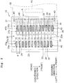
- the nozzle plate 20 includes nozzles 24. As depicted in Fig. 2 , the nozzles 24, from which an ink having any color of the four colors is jetted, are arrayed in the conveyance direction to form two nozzle arrays 25a, 25b arranged in the left-right direction.
- the nozzles 24 of the nozzle array 25a are arranged to deviate from the nozzles 24 of the nozzle array 25b in the conveyance direction by a half (P/2) of an arrangement pitch P of each nozzle array 25.
- the channel substrate 21 is made from silicon.
- the nozzle plate 20 is joined to a lower surface of the channel substrate 21.
- the channel substrate 21 includes pressure chambers 26 communicating with the nozzles 24, respectively.
- Each of the pressure chambers 26 has a rectangular planar shape elongated in the scanning direction.
- the pressure chambers 26 are arrayed in the conveyance direction while corresponding to the array of the nozzles 24 described above, thus forming two pressure chamber arrays 27 (27a and 27b) arranged in the left-right direction.
- the piezoelectric actuator 22 applies, to the ink in each pressure chamber 26, jetting energy for jetting the ink from each nozzle 24.
- the piezoelectric actuator 22 is disposed on an upper surface of the channel substrate 21.
- the piezoelectric actuator 22 includes a vibration film 30, piezoelectric elements 40, a protective film 34, an insulating film between layers 36 (hereinafter simply referred to as an insulating film 36), traces 35, and a trace protective film 37.
- a vibration film 30 piezoelectric elements 40
- a protective film 34 an insulating film between layers 36 (hereinafter simply referred to as an insulating film 36)
- traces 35 a trace protective film 37.
- a trace protective film 37 for the protective film 34 covering piezoelectric films 32 and the trace protective film 37 covering the traces 35 which are otherwise depicted in Figs. 3 to 5 .
- communicating holes 22a are formed in the piezoelectric actuator 22 at positions overlapping respectively with ends of the pressure chambers 26.
- the communicating holes 22a allow channels in the after-mentioned reservoir formation member 23 to communicate with the pressure chambers 26, respectively.
- the vibration film 30 is disposed on an entire area of the upper surface of the channel substrate 21 to cover the pressure chambers 26.
- the vibration film 30 is made from silicon dioxide (SiO 2 ), silicon nitride (SiN x ), or the like.
- the thickness of the vibration film 30 is, for example, approximately 1 ⁇ m.
- the piezoelectric elements 40 are disposed to face the pressure chambers 26 with the vibration film 30 being intervened therebetween. Namely, the piezoelectric elements 40, which are arrayed in the conveyance direction while corresponding to the array of the pressure chambers 26, form two piezoelectric element arrays 41 arranged in the scanning direction. Each of the piezoelectric elements 40 includes a lower electrode 31, the piezoelectric film 32, and an upper electrode 33.
- the lower electrode 31 is formed on an upper surface of the vibration film 30 to face the pressure chamber 26.
- a conductive film 38 is formed in an area between pressure chambers 26 by using the material which is the same as that used for the lower electrode 31.
- the conductive film 38 enables electrical conduction between the lower electrodes 31 of the pressure elements 40.
- a single large common electrode 39 which is formed by the lower electrodes 31 and the conductive films 38 disposed therebetween, is disposed on almost the entire area of the upper surface of the vibration film 30.
- the material of the lower electrodes 31 is not particularly limited, and it is possible to adopt, for example, a material having a two-layer structure of platinum (Pt) and titanium (Ti). In that case, a platinum layer may be approximately 200 nm and a titanium layer may be approximately 50 nm.
- Each piezoelectric film 32 is formed on the upper surface of the vibration film 30 via the lower electrode 31 in an area facing the pressure chamber 26. As depicted in Fig. 3 , the piezoelectric film 32 has such a planar shape as smaller than the pressure chamber 26 and elongated in the scanning direction.
- the piezoelectric film 32 is made from, for example, a piezoelectric material composed primarily of lead zirconate titanate (PZT) that is a mixed crystal of lead titanate and lead zirconate.
- the thickness of the piezoelectric film 32 is, for example, approximately 1 to 5 ⁇ m.
- Each upper electrode 33 has a rectangular planar shape that is slightly smaller than the piezoelectric film 32.
- the upper electrode 33 is formed on a central portion of an upper surface of the piezoelectric film 32.
- the upper electrode 33 is made from, for example, iridium (Ir).
- the thickness of the upper electrode 33 is, for example, approximately 80 nm.
- the protective film 34 which is arranged across the piezoelectric films 32 of the piezoelectric elements 40, extends over almost the entire area of the upper surface of the vibration film 30.
- the protective film 34 prevents moisture contained in the air from coming into the piezoelectric films 32.
- the protective film 34 is made from a waterproof material, such as alumina (Al 2 O 3 ).
- the thickness of the protective film 34 is, for example, approximately 80 nm. If moisture in the air comes into the piezoelectric films 32, then deterioration will occur in the piezoelectric films 32.
- the protective film 34 covering the piezoelectric films 32 prevents moisture from coming into the piezoelectric films 32.
- the protective film 34 includes rectangular openings 34a at parts overlapping with the central portions of the upper surfaces of the piezoelectric films 32 as viewed in a thickness direction of the protective film 34.
- the protective film 34 includes rectangular openings 34a at parts overlapping with the central portions of the upper surfaces of the piezoelectric films 32 as viewed in a thickness direction of the protective film 34.
- a large part of each upper electrode 33 is exposed from the protective film 34.
- the piezoelectric film 32 is not covered with the protective film 34, but covered with the upper electrode 33. Thus, moisture is prevented from coming into each piezoelectric film 32 from the outside.
- the insulating film 36 is formed on the protective film 34.
- the insulating film 36 includes openings 36a each of which is slightly larger than the opening 34a of the protective film 34.
- the insulating film 36 is disposed to cover a partition wall 28 partitioning pressure chambers 26 and a large part of the piezoelectric element 40 is exposed from the insulating film 36. Details of a formation range of the insulating film 36 around the piezoelectric element 40 will be described together with a formation range of the trace protective film 37.
- the insulating film 36 is provided primarily for improving the insulation quality between the conductive film 38 of the common electrode 39 and each trace 35. Without being limited to any particular material, the insulating film 36 is made from, for example, silicon dioxide (SiO 2 ). Further, from the point of view of securing the insulation quality between the common electrode 39 and each trace 35, the insulating film 36 preferably has a certain film thickness, such as from 300 to 500 nm.
- Each of the traces which is disposed on the insulating film 36, applies voltage to the corresponding one of the piezoelectric elements 40.
- the trace 35 is arranged with its one end hanging over an upper surface of a right end of the piezoelectric film 32 across the protective film 34 and insulating film 36.
- a conducting portion 55 is provided at parts, of the protective film 34 and the insulating film 36, covering a right end of the upper electrode 33 to penetrate through those films.
- the conducting portion 55 enables electrical conduction between the trace 35 and the right end of the upper electrode 33.
- the traces 35 corresponding to the piezoelectric elements 40 extend rightward respectively from the corresponding upper electrodes 33.
- the traces 35 are made from, for example, aluminum (Al).
- each of the traces 35 preferably has a certain thickness or more, such as approximately 1 ⁇ m.
- the insulating film 36 which is disposed under each trace 35, extends up to a right end of the channel substrate 21.
- drive contact portions 42 are arrayed on the insulating film 36 in the conveyance direction.
- the traces 35 which are drawn out rightward respectively from the upper electrodes 33, are connected to the drive contact portions 42.
- two ground contact portions 43 are arranged at the two opposite sides of the drive contact portions 42 in the conveyance direction.
- the ground contact portions 43 are connected to the common electrode 39 disposed on a lower side of the protective film 34 via conducting portions (not depicted) penetrating through the protective film 34 and the insulating film 36.
- the trace protective film 37 is formed on the insulating film 36 to cover each trace 35.
- the trace protective film 37 is provided for main purposes of protecting the trace 35 and securing the insulation between the traces 35.
- the trace protective film 37 is made from, for example, silicon nitride (SiN x ).
- the thickness of the trace protective film 37 is, for example, from 100 nm to 1 ⁇ m.
- the trace protective film 37 is formed with openings 37a like the insulating film 36.
- the opening 37a of the trace protective film 37 has substantially the same size as that of the opening 36a of the insulating film 36.
- the trace protective film 37 is disposed above the partition wall 28 partitioning pressure chambers 26 to cover each trace 35, and large parts of the piezoelectric elements 40 disposed at both sides of the trace 35 are exposed from the trace protective film 37.
- the opening 37a of the trace protective film 37 is slightly larger than the opening 34a of the protective film 34.
- the trace protective film 37 extends to the right end of the channel substrate 21 to cover a range including connection portions between the traces 35 and the drive contact portions 42. Meanwhile, the drive contact portions 42 and the ground contact portions 43 are exposed from the trace protective film 37, and they are electrically connected to an after-mentioned COF 50 that is to be joined to an upper surface of the right end of the channel substrate 21.
- the insulating film 36 is disposed above the partition wall 28 between two piezoelectric elements 40 adjacent to each other in the conveyance direction.
- the trace protective film 37 is disposed to cover each trace 35 disposed on the insulating film 36.
- both ends of the trace protective film 37 and the insulating film 36 in the conveyance direction are positioned inside ends of the partition wall 28.
- the trace protective film 37 and the insulating film 36 disposed above the partition wall 28 do not extend to areas facing the pressure chambers 26 partitioned by the partition wall 28.
- the ends of the insulating film 36 and the trace protective film 37 in the conveyance direction are not positioned above the pressure chambers 26.
- the vibration film 30 covering each pressure chamber 26 is prevented from having cracks starting at the ends of the trace protective film 37 and the insulating film 36.
- a width W of the trace protective film 37 and the insulating film 37 is preferably shorter than a width W1 of the partition wall 28 by 3.8 ⁇ m or longer. The reason thereof will be described later.
- etching for the trace protective film 37 and etching for the insulating film 36 are performed through the same step.
- the positions of the openings 37a of the trace protective film 37 are coincident with the positions of the openings 36a of the insulating film 36. This allows the ends of the trace protective film 37 and the ends of the insulting film 36 to be positioned at the same positions above the partition wall 28 in the conveyance direction.
- end positions of the trace protective film 37 slightly deviate from those of the insulating film 36 depending on taper shapes of film ends that are formed at the time of etching
- the above-described configuration in which the ends of the trace protective film 37 and the ends of the insulting film 36 are positioned at the same positions includes a case in which such a slight deviation is present.
- a formation range of the films 36, 37 in the scanning direction i.e., a longitudinal direction of the pressure chamber 26 will be described with reference to Fig. 4 .
- the piezoelectric element 40 When the piezoelectric element 40 is deformed, stress is more likely to concentrate on positions of the vibration film 30 overlapping with ends of the piezoelectric film 32 in the longitudinal direction.
- the insulating film 36 and the trace protective film 37 are formed to the above positions. Namely, as depicted in Figs. 3 and 4 , the insulating film 36 and the trace protective film 37 are disposed to overlap with both ends of the pressure chamber 26 in the longitudinal direction.
- This configuration allows the ends of the piezoelectric film 32 to be covered with the insulating film 36 and the trace protective film 37, thus increasing rigidity at those positions. Further, this configuration makes bending in the vicinities of ends of the pressure chamber 26 in the longitudinal direction gentle, thus preventing a crack in the vibration film 30.
- the vibration film 30 is more likely to have cracks starting at the ends of the films 36 and 37, like the case in which the films 36 and 37 extend beyond each pressure chamber 26 in the lateral direction of the pressure chamber 26.
- the ends of the trace protective film 37 and the insulating film 36 extend over or cover the upper surface of each piezoelectric film 32, thus preventing cracks starting at the ends of the films 36, 37.
- the vibration film 30 may be prevented from being displaced in a case of driving the piezoelectric element 40.
- This problem is more likely to be caused in film parts in the lateral direction of the pressure chamber 26 that has great influence on the displacement, and the problem is less likely to be caused in the film ends in the longitudinal direction that has small influence on the displacement.
- the present embodiment adopts a configuration in which the trace protective film 37 and the insulating film 36 partially overlap with each piezoelectric chamber 26 and each piezoelectric film 32 in the longitudinal direction of the pressure chamber 26 to reliably prevent the vibration film 30 from having a crack.
- the Chip On Film (COF) 50 which is a wiring member, is joined to an upper surface of a right end of the piezoelectric actuator 22. Traces 55a formed in the COF 50 are electrically connected to the drive contact portions 42, respectively.
- the controller 6 (see Fig. 1 ) of the printer 1 is connected to the other end of the COF 50 than the end connected to the drive contact portions 42. Further, a driver IC 51 is mounted on the COF 50.
- the driver IC 51 Based on a control signal sent in from the controller 6, the driver IC 51 generates and outputs a drive signal for driving the piezoelectric actuator 22.
- the drive signal output from the driver IC 51 is input to the drive contact portions 42 via the traces 55a of the COF 50 and supplied to the respective upper electrodes 33 via the traces 35 of the piezoelectric actuator 22.
- the upper electrodes 33 supplied with the drive signal change in potential between a predefined drive potential and a ground potential.
- the COF 50 is formed with a ground trace (not depicted), and the ground trace is electrically connected to the ground contact portions 43 of the piezoelectric actuator 22. This allows the common electrode 31 connected to the ground contact portions 43 to be constantly kept at the ground potential.
- the piezoelectric actuator 22 when supplied with the drive signal from the driver IC 51. Without being supplied with the drive signal, the upper electrodes 33 stay at the ground potential and thus have the same potential as the common electrode 39. From this state, if the drive signal is supplied to any of the upper electrodes 33 to apply the drive potential to that upper electrode 33, then due to the potential difference between that upper electrode 33 and the common electrode 39, the piezoelectric film 32 is acted on by an electric field parallel to its thickness direction. On that occasion, piezoelectric reverse effect makes the piezoelectric film 32 to extend in its thickness direction and to contract in its planar direction. Further, along with the contraction deformation of the piezoelectric film 32, the vibration film 30 bows to project toward the pressure chamber 26. By virtue of this, the pressure chamber 26 decreases in volume to produce a pressure wave inside the pressure chamber 26, thereby jetting liquid drops of the ink from the nozzle 24 in communication with the pressure chamber 26.
- the reservoir formation member 23 is disposed on the far side (the upper side) of the piezoelectric actuator 22 from the channel substrate 21 across the piezoelectric actuator 22, and joined to the upper surface of the piezoelectric actuator 22 by way of adhesive. While the reservoir formation member 23 may be made from silicon, for example, as with the channel substrate 21, it may also be made from other materials than silicon, such as a metallic material or a synthetic resin material.
- the reservoir formation member 23 has an upper half portion formed with a reservoir 52 extending in the conveyance direction. Through non-depicted tubes, the reservoir 52 is connected to the cartridge holder 7 (see Fig. 1 ) in which the ink cartridges 17 are installed.
- the reservoir formation member 23 has a lower half portion formed with ink supply channels 53 extending downward from the reservoir 52.
- the ink supply channels 53 are in respective communication with the communicating holes 22a of the piezoelectric actuator 22.
- a concave protective cover 54 is also formed in the lower half portion of the reservoir formation member 23 to cover the piezoelectric elements 40 of the piezoelectric actuator 22.
- the vibration film 30 of silicon dioxide is formed on a surface of the channel substrate 21 that is a silicon substrate.
- the common electrode 39 which will be the lower electrodes 31, is formed as a film on the vibration film 30 by way of sputtering or the like.
- a piezoelectric material film 59 which is made from a piezoelectric material such as PZT, is formed on the entire area of the upper surface of the common electrode 39, by way of a sol-gel method, sputtering, or the like.
- the upper electrodes 33 are formed on the upper surface of the piezoelectric material film 59.
- an electroconductive film 57 is formed on the upper surface of the piezoelectric material film 59 by way of sputtering or the like.
- the upper electrodes 33 are formed on the upper surface of the piezoelectric material film 59.
- the piezoelectric material film 59 is etched to form the piezoelectric films 32, thus forming the piezoelectric elements 40 on the vibration film 30.
- the common electrode 39 is etched to form a hole 31a to construct part of each of the communicating holes 22a (see Fig. 4 ) of the piezoelectric actuator 22.
- the protective film 34 is formed by way of sputtering or the like to cover the piezoelectric elements 40.
- the insulating film 36 is formed on the protective film 34.
- the insulating film 36 is formed to cover the piezoelectric elements 40 as well as the partition walls 28 provided between the adjacent piezoelectric elements 40. It is possible to form the insulating film 36 made from silicon dioxide by way of plasma CVD as preferred.
- a hole 56 is formed by way of etching in such a part, of the protective film 34 and insulating film 36, covering an end of each of the upper electrodes 33.
- the holes 56 serve for electrical conduction between the upper electrodes 33 and the traces 35 to be formed on the insulating film 36 in the next step.
- the traces 35 are formed on the insulating film 36 upon the protective film 34.
- an electroconductive film 58 is formed on the upper surface of the insulating film 36 by way of sputtering or the like.
- the holes 56 are filled with part of an electroconductive material to form a conducting portion 55 in each of the holes 56 to electrically conduct the upper electrodes 33 and the electroconductive film 58.
- the electroconductive film 58 is etched to remove unnecessary parts and form the traces 35.
- the trace protective film 37 is formed to cover the piezoelectric elements 40 and the traces 35 connected to the piezoelectric elements 40 respectively.
- the trace protective film 37 made from silicon nitride (SiN x ) is preferably formed by way of plasma CVD.
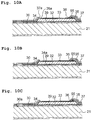
- the trace protective film 37 and the insulating film 36 are etched to remove, at a time, such parts of the trace protective film 37 and the insulating film 36 that overlap with the piezoelectric elements 40.
- the openings 37a are formed in the trace protective film 37 while the openings 36a are formed in the insulating film 36 to expose the protective film 34 thereunder.
- removal of the trace protective film 37 and the insulating film 36 is performed as follows. At first, a mask covering areas other than the formation areas of the openings 36a, 37a is formed on a surface of the trace protective film 37 through photoresist. After forming the mask, etching is performed from the surface of the trace protective film 37 to remove the trace protective film 37 and the insulating film 36 at a time. Then, the openings 36a, 37a are formed in areas, of the two kinds of films 36 and 37, which are not covered with the mask. After the etching, the mask is released and removed.
- the insulating film 36 disposed under the trace 35 and the trace protective film 37 covering the trace 35 from above are not removed but remain in an area including the partition wall 28 partitioning two pressure chambers 26 adjacent to each other in the conveyance direction. In that case, the ends of the insulating film 36 and the trace protective film 37 are formed not to extend beyond the ends of the partition wall 28.
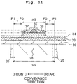
- the removal step is performed by setting a target formation position P0 for an end of the insulating film 36 and the trace protective film 37 in the conveyance direction at the inside of a target formation position P1 for an end of the partition wall 28.
- the target formation position of an end of the films 36, 37 means a target position of an end of the films 36, 37 in a case of etching them, and thus a mask position, an etching amount, and the like are adjusted to position the end of the films 36, 37 in the target position.
- the target formation position of an end of the partition wall 28 means a target position of an end of the partition wall 28 when the channel substrate 21 is etched to form the pressure chamber 26 in a step of forming the pressure chamber 26 as described later ( Fig. 12B ), and thus a mask position, an etching amount, and the like are adjusted to position the end of the partition wall 28 in the target position.
- the "target formation positions” mean positions (sizes) that are explicitly stated in a design drawing for manufacture of the head unit.
- various kinds of deviations caused during etching for the films 36,37 may cause deviations of the ends of the films 36, 37 from the target formation positions P0 as depicted by two-dot chain lines in Fig. 11 .
- various kinds of deviations caused when etching is performed to form the pressure chamber 26 may cause deviations of the ends of the partition wall 28 from the target formation positions P1.
- the ends of the films 36, 37 after processing may not be positioned inside the ends of the partition wall 28.
- the inventors of the present application manufactured a head unit in such a setting in which the ends of the films 36, 37 are coincident with the the ends of the partition wall 28, and they conducted a drive test.
- the vibration film 30 cracked during the test.
- the thickness of the vibration film 30 of this trial product is from 1.0 to 1.4 ⁇ m.
- the target formation position P0 for the end of the films 36, 37 is preferably positioned inside the target formation position P1 for the end of the partition wall 28 by not less than 3 ⁇ m. The reason thereof is as follows.
- a mask deviation causes a position (a) of the films disposed above the partition wall 28 to vary, and a processing deviation during etching causes a film width (b) to vary. Those variations may cause positions of ends of the films 36, 37 to deviate.
- a mask deviation causes a position (c) of the partition wall 28 to vary and the processing deviation during etching causes a width (d) of the partition wall 28 to vary. Those variations may cause positions of ends of the partition wall 28 to deviate.
- a distance T between an end position of the films 36, 37 and an end position of the partition wall 28 varies within a certain range.
- the target formation position P0 for the end of the films 36, 37 is preferably set in such a manner that, even when various kinds of deviations have occurred, the actual end position of the films 36, 37 is positioned inside the target formation position P1 for the end of the partition wall 28.
- degrees of various deviations described above depend on the precision of an apparatus to be used for etching the films 36, 37 and forming the pressure chamber 26, they may have values indicated in Table 1.
- the values in Table 1 indicate values for 3 ⁇ , and the probability that deviations are within that range is 99.7%.
- “mask deviation” means the degree of a position deviation caused when an etching mask deviates in parallel with respect to a planer direction;
- “processing deviation” means the degree of a width deviation caused by etching processing.
- “mask deviation in pressure chamber formation is + 3 ⁇ m” means that the etching mask deviates from a target setting position by a maximum of 3 ⁇ m when the channel substrate 21 is etched to form the pressure chamber 26.
- removing the insulating film 36 and the trace protective film 37 at a time reduces the number of removal steps. This means that opportunities causing the mask deviation and processing deviation are reduced.
- removal of the two kinds of films 36, 37 are performed individually, two removal steps are required. Thus, the mask deviation and processing deviation may be caused in respective two removal steps, increasing the total deviation amount.
- the target formation position P0 is preferably determined based on "square sum of common difference (square sum of tolerance)".
- four kinds of sizes (a to d) indicated in Table 1 do not interfere with each other. Namely, a to d are independent subjects.
- a distribution T 2 of the distance T is represented by the following formula in accordance with distribution additivity.
- T 2 a 2 + b 2 2 + c 2 + d 2 2
- the processing deviations (b), (d) indicated in Table 1 mean width deviation values including the film width and partition wall width. Thus, when a deviation amount of an end position is determined, a half value of the width deviation value is used for the width deviation, as indicated in Formula 1.
- T is 3.17. Since the a to d values are values for 3 ⁇ , T is not more than 3.17 ⁇ m with 99.7% probability. In a practical way, when the target formation position P0 of the end of the films 36, 37 is set inside the target formation position P1 of the end of the partition wall 28 by not less than 3 ⁇ m, the films 36, 37 do not extend beyond the ends of the partition wall 28.
- the target formation position P0 of the end of the films 36, 37 disposed above the partition wall 28 may be expressed by a relation with the dimension of the partition wall 28.
- the array pitch of the pressure chambers 26 is 84.7 ⁇ m (size A in Fig. 5 ).
- the pressure chamber 26 is preferably 60 to 70 ⁇ m in width (size B in Fig. 5 ).
- the partition wall 28 partitioning two pressure chambers 26 may be 14.7 to 24.7 ⁇ m in width (size C in Fig. 5 ).
- setting the target formation position P0 of the end of the films 36, 37 at a position having 3 ⁇ m distance from the target formation position P1 of the partition wall 28 has the same meaning as setting the distance between P0 and P1 to be 12% (3 ⁇ m /24.7 ⁇ m) to 20% (3 ⁇ m/12.7 ⁇ m) of the width of the partition wall 28.
- the distance may be set to be not less than 12% of the width of the partition wall 28.
- the relation between the width of the films 36, 37 and the width of the partition wall 28 after performing the removal step of the films 36, 37 is as follows.
- the width W of the films 36, 37 depicted in Fig. 6 is theoretically reduced by 6 ⁇ m in total, specifically 3 ⁇ m each on the left and right sides, as compared to the width W1 of the partition wall 28.
- the relation between the width W of the films 36, 37 to be actually formed and the width W1 of the partition wall 28 is determined as follows.
- W ⁇ W 1 ⁇ 3 ⁇ m ⁇ 2 + 0.2 ⁇ m + 2 ⁇ m W 1 ⁇ 3.8 ⁇ m
- the step of removing the trace protective film 37 and the insulating film 36 is completed in the step of Fig. 10A .
- the protective film 34 exposed from the trace protective film 37 and the insulating film 36 is etched to form the opening 36a in the protective film 34.
- the vibration film 30 is etched to form a hole 30a that is a part of the communicating hole 22a (see Fig. 4 ) of the piezoelectric actuator 22.
- Manufacture of the piezoelectric actuator 22 is completed in the step of Fig. 10C .
- the channel substrate 21 in which ink channels are to be formed is partially removed by being polished from a lower surface side (on the side opposite to the vibration film 30), thus reducing the thickness of the channel substrate 21 to have a predefined thickness.
- a silicon wafer that is an original of the channel substrate 21 has a thickness of approximately 500 to 700 ⁇ m
- the channel substrate 21 is polished to have a thickness of approximately 100 ⁇ m during the polish step.
- etching is performed for the channel substrate 21 from the lower surface side that is opposite to the side of the vibration film 30, thus forming the pressure chamber 26.
- the etching for the channel substrate 21 may be wet etching or dry etching. In general, however, dry etching generates not only chemical reactivity but also physical reactivity, and thus the vibration film 30 may be etched to have a thickness smaller than a target thickness. Accordingly, the present teaching is especially preferably used in a case of forming the pressure chamber 26 through dry etching.
- the nozzle plate 20 is joined to the lower surface of the channel substrate 21 with adhesive.
- the reservoir formation member 23 is joined to the piezoelectric actuator 22 with adhesive.
- the conveyance direction and the lateral direction of the pressure chamber 26 correspond to "first direction” of the present teaching
- the scanning direction and the longitudinal direction of the pressure chamber 26 correspond to “second direction” of the present teaching
- Two pressure chambers 26 of the right-side pressure chamber array 27b correspond to "first pressure chamber” and “second pressure chamber” of the present teaching.
- the vibration film 30 corresponds to "first insulating film” of the present teaching.
- Two piezoelectric elements 40 of the right-side piezoelectric element array 41b correspond to "first piezoelectric element” and “second piezoelectric element” of the present teaching.
- the trace protective film 37 corresponds to "second insulating film” of the present teaching.
- the insulating film between layers 36 corresponds to "third protective film” of the present teaching.
- the step of forming the trace protective film 37 depicted in Fig. 9C corresponds to "first-order insulating film formation step" of the present teaching.
- the step of forming the insulating film 36 depicted in Fig. 8D corresponds to "second-order insulating film formation step” of the present teaching.
- the step of removing the trace protective film 37 and the insulating film 36 correspond to "first removal step” of the present teaching.
- the common electrode 39 including the lower electrodes 31 and the conductive films 38 is formed on the almost entire area of the upper surface of the vibration film 30.
- Each of the conductive films 38 is disposed on the corresponding one of the partition walls 28 (see Fig. 5 ).
- great tensile stress acting in a planer direction of the channel substrate 21 remains on each piezoelectric element 40 and the channel substrate 21.
- the tensile stress is one of the factors obstructing deformation of the piezoelectric element 40.
- the common electrode 39 may be patterned to be formed with openings 39a between piezoelectric elements 40 arranged in the conveyance direction. This prevents the common electrode 39 from contracting entirely and greatly, thus reducing the tensile stress.
- the ends of the insulating film 36 and the trace protective film 37 are preferably positioned inside the ends of the partition wall 28 for the purpose of preventing the vibration film 30 from having a crack.
- the pressure chambers 26 form two pressure chamber arrays 27, and the piezoelectric elements 40 are also arranged in two arrays corresponding to the arrangement of the pressure chambers 26.
- the number of arrays of the pressure chambers 26 and the piezoelectric elements 40 is not limited to two arrays.
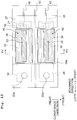
- the number of arrays of the pressure chambers 26 and the piezoelectric elements 40 may be four arrays. Traces 35 are connected to the respective piezoelectric elements 40 forming the four piezoelectric element arrays 41 (41a to 41d), and all of the traces 35 are drawn out rightward. In that configuration, the number of traces 35 arranged between the piezoelectric elements 40 is different between the four piezoelectric element arrays 41.
- each of the four piezoelectric element arrays 41 the insulating film 36 and the trace protective film 37 are formed between the piezoelectric elements 40 adjacent to each other in the conveyance direction.
- the piezoelectric element array 41a positioned at the leftmost end has no traces 35 arranged between adjacent piezoelectric elements 40.
- the trace protective film 37 is formed above each partition wall 28, as with other piezoelectric element arrays 41.
- the width of the insulating film 36 and the trace protective film 37 may depend on the number of traces 35.
- the width of the insulating film 36 and the trace protective film 37 disposed above the partition wall 28 is different between the four piezoelectric element arrays 41, the distance between the end of the films 36, 37 and the end of the partition wall 28, namely, the distance to the end of the pressure chamber 26 is different between the four piezoelectric element arrays 41. This causes displacement of the vibration film 30 to vary between the piezoelectric elements 40, thus leading to unevenness of jetting characteristics between the nozzles 24.
- the four piezoelectric element arrays 41 are preferably configured such that parts of the films 36 and 37 covering the traces 35 are identical in width. Namely, in the removal step for the films 36 and 37, the target formation position P0 of the end of the films 36, 37 is set to be common between the four piezoelectric element arrays 41. This allows the four piezoelectric element arrays 41 to have almost the same distance from the end of the partition wall 28 to the end of the films 36 and 37, thus uniformizing jetting characteristics.
- two pressure chambers 26 belonging to one pressure chamber array 27 correspond to "first pressure chamber” and “second pressure chamber” of the present teaching.
- Two pressure chambers 26 belonging to another pressure chamber array 27 correspond to "third pressure chamber” and “fourth pressure chamber” of the present teaching.
- Two piezoelectric elements 40 corresponding to the one pressure chamber array 27 correspond to "first piezoelectric element” and “second piezoelectric element” of the present teaching.
- Two piezoelectric elements 40 corresponding to the another pressure chamber array 27 correspond to "third piezoelectric element” and "fourth piezoelectric element” of the present teaching.
- the insulating film 36 and the trace protective film 37 are removed through etching at a time, the insulating film 36 and the trace protective film 37, however, may be removed through different steps.
- the step of removing the trace protective film 37 corresponds to "first removal step” of the present teaching
- the step of removing the insulating film 36 corresponds to "second removal step” of the present teaching.
- each trace 35 covered with the trace protective film 37 is a trace for applying driving potential to the piezoelectric element 40.
- the trace 35 is not limited to such a trace.
- each trace 35 may be a ground trace connected to the common electrode.
- the lower electrodes that are conducted to each other between the piezoelectric elements form the common electrode
- the upper electrodes are individual electrodes provided separately for each of the piezoelectric elements.
- the present teaching is not limited thereto.
- the lower electrodes may be individual electrodes, and the upper electrodes may form the common electrode.
- the piezoelectric actuator 22 of the above embodiment includes two kinds of films: the insulating film 36 and the trace protective film 37.
- the present teaching is not limited thereto.
- the piezoelectric actuator 22 may include any one of the insulating film 36 and the trace protective film 37.
- the insulating film 36 may not be formed at least above the partition wall 28.
- the trace protective film 37 covering the traces 35 is preferably provided to prevent corrosion and the like.
- the trace protective film 37 may not be formed.
- the present teaching is applied to the ink-jet head that discharges ink on the recording sheet to print an image or the like thereon.
- the present teaching may be applied to a liquid discharge apparatus that is used in various ways of use other than the print of the image or the like.
- the present teaching can be also applied, for example, to a liquid discharge apparatus that discharges a conductive liquid onto a substrate to form a conductive pattern on a surface of the substrate.
Landscapes
- Engineering & Computer Science (AREA)
- Manufacturing & Machinery (AREA)
- Particle Formation And Scattering Control In Inkjet Printers (AREA)
Abstract
Description
- The present invention relates to a liquid jetting apparatus and a method of producing the liquid jetting apparatus.
- As a liquid jetting apparatus jetting liquid, Japanese Patent Application laid-open No.
2003-159798 - The pressure chambers of the head main body form four pressure chamber arrays arranged in a main scanning direction of the ink-jet head. The piezoelectric actuator includes a vibration plate covering the pressure chambers, a common electrode formed on the vibration plate, a piezoelectric body disposed on the common electrode, and individual electrodes disposed on the upper surface of the piezoelectric body while corresponding to the pressure chambers. It can be said that, each individual electrode, the common electrode, and a part of the piezoelectric body sandwiched between the two kinds of electrodes are disposed to face one pressure chamber, thus forming one piezoelectric element. Namely, the piezoelectric actuator includes the piezoelectric elements that are arranged in four arrays while corresponding to the pressure chambers.
- The individual electrodes of the piezoelectric elements are connected to traces. Each of the traces is led from the corresponding one of the individual electrodes to the outside in the main scanning direction. In two piezoelectric element arrays at one side, traces connected to the individual electrodes of a piezoelectric element array disposed at the inside in the main scanning direction extend to the outside while running between two piezoelectric elements of a piezoelectric element array disposed at the outside in the main scanning direction. An end of each trace is provided with a pressure input terminal.
- Meanwhile, although it is not described in Japanese Patent Application laid-open No.
2003-159798 - Inventors of the present application made an experimental actuator having a configuration in which the insulating film partially covers the pressure chambers from above, and then conducted a drive test. As a result, it has been revealed that the vibration plate has cracks starting at end positions of the insulating film.
- An object of the present teaching is to prevent a film covering pressure chambers from having a crack which would be otherwise caused by a configuration in which an insulating film formed above a partition wall partially covers the pressure chambers from above.
- According to a first aspect of the present teaching, a liquid jetting apparatus is characterized by including: a first pressure chamber and a second pressure chamber arranged in a first direction;
a first insulating film covering the first pressure chamber and the second pressure chamber;
a first piezoelectric element arranged to face the first pressure chamber so that the first insulating film is intervened between the first pressure chamber and the first piezoelectric element;
a second piezoelectric element arranged to face the second pressure chamber so that the first insulating film is intervened between the second pressure chamber and the second piezoelectric element;
at least one trace arranged between the first piezoelectric element and the second piezoelectric element which are adjacent to each other in the first direction; and
a second insulating film covering the at least one trace,
wherein an end, in the first direction, of a part of the second insulating film covering the at least one trace between the first piezoelectric element and the second piezoelectric element is positioned inside an end of a partition wall partitioning the first pressure chamber and the second pressure chamber. - In the present teaching, the end of the part of the second insulating film covering the at least one trace between the first piezoelectric element and the second piezoelectric element is positioned inside the end of the partition wall partitioning the first pressure chamber and the second pressure chamber. Thus, between the first piezoelectric element and the second piezoelectric element, the second insulating film does not overlap with the first pressure chamber and the second pressure chamber. In such a configuration, the end of the second insulating film is not positioned on each pressure chamber, and thus stress is less likely to concentrate on the first insulating film covering each pressure chamber. This prevents the first insulating film from having a crack.
- The liquid jetting apparatus according to the first aspect of the present teaching, may further include a third insulating film arranged between the partition wall and the at least one trace,
wherein, between the first piezoelectric element and the second piezoelectric element, an end of the third insulating film in the first direction may be positioned inside the end of the partition wall. - In the liquid jetting apparatus according to the first aspect of the present teaching, between the first piezoelectric element and the second piezoelectric element, the end of the second insulating film in the first direction and the end of the third insulating film in the first direction may be in the same position in the first direction.
- In the liquid jetting apparatus according to the first aspect of the present teaching, an end of the second insulating film in a second direction orthogonal to the first direction may be arranged in an area facing the first pressure chamber and the second pressure chamber to extend over upper surfaces of piezoelectric films of the first piezoelectric element and the second piezoelectric element.
- In the liquid jetting apparatus according to the first aspect of the present teaching, a width, in the first direction, of the part of the second insulating film covering the at least one trace between the first piezoelectric element and the second piezoelectric element may be shorter than a width of the partition wall by 3.8 µm or longer.
- The liquid jetting apparatus according to the first aspect of the present teaching, may further include:
- a third pressure chamber and a fourth pressure chamber arranged in the first direction;
- a third piezoelectric element arranged to face the third pressure chamber so that the first insulating film is intervened between the third pressure chamber and the third piezoelectric element;
- a fourth piezoelectric element arranged to face the fourth pressure chamber with the first insulating film being intervened therebetween; and
- wherein the number of traces arranged between the first piezoelectric element and the second piezoelectric element may be different from the number of traces arranged between the third piezoelectric element and the fourth electric element, and a width of the part of the second insulating film covering the at least one trace between the first piezoelectric element and the second piezoelectric element may be identical to a width of a part of the second insulating film covering the at least one trace between the third piezoelectric element and the fourth piezoelectric element.
- According to a second aspect of the present teaching, a liquid jetting apparatus is characterized by including:
- a first pressure chamber and a second pressure chamber arranged in a first direction;
- a first insulating film covering the first pressure chamber and the second pressure chamber;
- a first piezoelectric element arranged to face the first pressure chamber with the first insulating film being intervened therebetween;
- a second piezoelectric element arranged to face the second pressure chamber with the first insulating film being intervened therebetween;
- a trace arranged between the first piezoelectric element and the second piezoelectric element which are adjacent to each other in the first direction; and
- a third insulating film arranged between the trace and a partition wall partitioning the first pressure chamber and the second pressure chamber,
- wherein, between the first piezoelectric element and the second piezoelectric element, an end of the third insulating film in the first direction is positioned inside an end of the partition wall.
- According to a third aspect of the present teaching, a method of producing a liquid jetting apparatus, is characterized by including:
- a first-order insulating film formation step of forming a second insulating film on a channel substrate which includes: a first insulating film; a first piezoelectric element and a second piezoelectric element arranged on the first insulating film while corresponding to a first pressure chamber and a second pressure chamber that are arranged in a first direction; and at least one trace arranged between the first piezoelectric element and the second piezoelectric element, wherein the second insulating film is formed on the channel substrate to cover the first piezoelectric element, the second piezoelectric element, and the at least one trace; and
- a first removal step of removing a part of the second insulating film covering the first piezoelectric element and the second piezoelectric element,
- wherein, in the first removal step, the second insulating film is removed by setting a target formation position of an end, in the fi rst direction, of a part of the second insulating film covering the at least one trace between the first piezoelectric element and the second piezoelectric element, at a position inside a target formation position of an end of a partition wall partitioning the first pressure chamber and the second pressure chamber.
- In the method of producing the liquid jetting apparatus according to the third aspect of the present teaching, in the first removal step, the second insulating film may be removed by setting the target formation position of the end, in the first direction, of the part of the second insulating film covering the at least one trace, at a position inside the target formation position of the end of the partition wall by 3 µm or longer.
- In the method of producing the liquid jetting apparatus according to the third aspect of the present teaching, in the first removal step, the second insulating film may be removed by setting the target formation position of the end, in the first direction, of the part of the second insulating film covering the at least one trace, at a position having a distance to the target formation position of the end of the partition wall which is greater than a width of the partition wall by 12% or more.
- The method of producing the liquid jetting apparatus according to the third aspect of the present teaching, may further includes:
- a second-order insulating film formation step of forming, before formation of the at least one trace on the channel substrate, a third insulating film to cover the first piezoelectric element, the second piezoelectric element, and the partition wall; and
- a second removal step of removing a part of the third insulating film covering the first piezoelectric element and the second piezoelectric element,
- wherein, in the second removal step, the third insulating film is removed by setting a target formation position of an end, in the first direction, of the third insulating film between the first piezoelectric element and the second piezoelectric element, at a position inside the target formation position of the end of the partition wall.
- In the method of producing the liquid jetting apparatus according to the third aspect of the present teaching, in the first removal step, the part of the second insulating film covering the first piezoelectric element and the second piezoelectric element and the part of the third insulating film covering the first piezoelectric element and the second piezoelectric element may be removed at a time.
- In the method of producing the liquid jetting apparatus according to the third aspect of the present teaching, in the channel substrate, a third piezoelectric element and a fourth piezoelectric element may be formed on the first insulating film while corresponding to a third pressure chamber and a fourth pressure chamber which are arranged in the first direction;
the number of traces arranged between the first piezoelectric element and the second piezoelectric element may be different from the number of traces arranged between the third piezoelectric element and the fourth piezoelectric element;
in the first-order insulating film formation step, the second insulating film may be formed to cover the third piezoelectric element, the fourth piezoelectric element, and the at least one trace arranged between the third piezoelectric element and the fourth piezoelectric element, and then, in the first removal step, a part of the second insulating film covering the third piezoelectric element and the fourth piezoelectric element may be removed; and
in the first removal step, the second insulating film may be removed in such a manner that a width of the part of the second insulating film covering the at least one trace between the first piezoelectric element and the second piezoelectric element is identical to a width of a part of the second insulating film covering the at least one trace between the third piezoelectric element and the fourth piezoelectric element. - According to a fourth aspect of the present teaching, a method of producing a liquid jetting apparatus, is characterized by including:
- a second-order insulating film formation step of forming, on a channel substrate formed with a first insulating film, a first piezoelectric element, and a second piezoelectric element, the first and second piezoelectric elements being disposed on the first insulating film while corresponding to a first pressure chamber and a second pressure chamber arranged in a first direction, a third insulating film to cover the first piezoelectric element, the second piezoelectric element, and a partition wall partitioning the first pressure chamber and the second pressure chamber;
- a trace formation step of forming, on the third insulating film, a trace arranged between the first piezoelectric element and the second piezoelectric element; and
- a second removal step of removing a part of the third insulating film covering the first piezoelectric element and the second piezoelectric element,
- wherein, in the second removal step, the third insulating film is removed by setting a target formation position of an end, in the first direction, of a part of the third insulating film between the first piezoelectric element and the second piezoelectric element, at a position inside a target formation position of an end of the partition wall.
-
-
Fig. 1 is a schematic plan view of a printer according to an embodiment of the present teaching. -
Fig. 2 is a top view of a head unit of an ink-jet head. -
Fig. 3 is an enlarged view depicting a portion A ofFig. 2 . -
Fig. 4 is a cross-sectional view taken along a line IV-IV ofFig. 3 . -
Fig. 5 is a cross-sectional view taken along a line V-V ofFig. 3 . -
Fig. 6 is an enlarged view depicting surroundings of a partition wall ofFig. 5 . -
Fig. 7A depicts a step of forming a vibration film,Fig. 7B depicts a step of forming a common electrode as a film,Fig. 7C depicts a step of forming a piezoelectric material film,Fig. 7D depicts a step of forming a conductive film for an upper electrode, andFig. 7E depicts a step of etching the conductive film (a step of forming the upper electrode). -
Fig. 8A depicts a step of etching the piezoelectric material film (a step of forming a piezoelectric element),Fig. 8B depicts a step of etching the common electrode,Fig. 8C depicts a step of forming a protective film,Fig. 8D depicts a step of forming an insulating film between layers, andFig. 8E depicts a step of forming a hole for electrical conduction between the upper electrode and a trace. -
Fig. 9A depicts a step of forming a conductive film for the trace,Fig. 9B depicts a step of etching the conductive film (a step of forming the trace), andFig. 9C depicts a step of forming a trace protective film. -
Fig. 10A depicts a step of partially removing the insulating film between layers and the trace protective film,Fig. 10B depicts a step of partially removing the protective film, andFig, 10C depicts a step of forming a hole of a vibration plate. -
Fig. 11 illustrates the step of removing the insulating film between layers and the trace protective film. -
Fig. 12A depicts a step of polishing a channel substrate,Fig. 12B depicts a step of etching the channel substrate (a step of forming the pressure chamber),Fig, 12C depicts a joining step of a nozzle plate, andFig. 12D depicts a joining step of a reservoir formation member. -
Fig. 13 is a partially enlarged top view depicting a head unit according to a modified embodiment of the present teaching. -
Fig. 14 is a plan view of a common electrode of the head unit depicted inFig. 13 . -
Fig. 15 is a cross-sectional view taken along a line XV-XV ofFig. 13 . -
Fig. 16 is a top view of a head unit according to another modified embodiment of the present teaching. -
Fig. 17A is a cross-sectional view taken along a line A-A ofFig. 16 ,Fig. 17B is a cross-sectional view taken along a line B-B ofFig. 16 ,Fig. 17C is a cross-sectional view taken along a line C-C ofFig. 16 , andFig. 17D is a cross-sectional view taken along a line D-D ofFig. 16 . - Subsequently, an embodiment of the present teaching will be described.
Fig. 1 is a schematic plan view of a printer according to the present embodiment. At first, a schematic configuration of an ink-jet printer 1 will be explained with reference toFig. 1 . The respective front, rear, left, and right directions depicted inFig. 1 are defined as "front", "rear", "left", and "right" of the printer. Further, a front side of each paper surface is defined as "up" or upward", and a rear side of each paper surface is defined as "down" or "downward". In the following, the explanation will be made by appropriately using the front (side), the rear (side), the left (side), the right (side), the up (upper side), and the down (lower side) defined as described above. - As depicted in
Fig. 1 , the ink-jet printer 1 includes aplaten 2, acarriage 3, an ink-jet head 4, a conveyance mechanism 5, acontroller 6, and the like. - A
recording sheet 100 as a recording medium is placed on an upper surface of theplaten 2. Thecarriage 3 is configured to reciprocate in a left-right direction (hereinafter referred to as a scanning direction) in an area facing theplaten 2 along twoguide rails endless belt 14 is connected to thecarriage 3, and acarriage drive motor 15 drives theendless belt 14 to move thecarriage 3 in the scanning direction. - The ink-
jet head 4, which is installed to thecarriage 3, moves in the scanning direction together with thecarriage 3. The ink-jet head 4 includes fourhead units 16 arranged in the scanning direction. The fourhead units 16 are connected, via unillustrated tubes, to acartridge holder 7 to whichink cartridges 17 of four colors (black, yellow, cyan, and magenta) are installed. Each of thehead units 16 includes nozzles 24 (seeFigs. 2 to 5 ) formed on a lower surface thereof (the rear side of the paper surface ofFig. 1 ). Each of the inks supplied from the corresponding one ofink cartridges 17 is jetted fromnozzles 24 of each of thehead units 16 to therecording sheet 100 placed on theplaten 2. - The conveyance mechanism 5 includes two
conveyance rollers platen 2 in a front-rear direction. The conveyance mechanism 5 conveys therecording sheet 100 placed on theplaten 2 frontward (hereinafter also referred to as a conveyance direction) by use of the twoconveyance rollers - The
controller 6 includes a Read Only Memory (ROM), a Random Access Memory (RAM), an Application Specific Integrated Circuit (ASIC) including various control circuits, and the like. Thecontroller 6 controls the ASIC to execute a variety of processing, such as printing for therecording sheet 100, in accordance with programs stored in the ROM. For example, in the print processing, thecontroller 6 controls the ink-jet head 4, thecarriage drive motor 15, and the like to perform printing of an image or the like on therecording sheet 100 based on a printing command input from an external apparatus, such as a PC. In particular, thecontroller 6 alternately performs an ink jetting operation in which the ink-jet head 4 jets ink while moving in the scanning direction together with thecarriage 3 and a conveyance operation in whichconveyance rollers recording sheet 100 in the conveyance direction by a predefined amount. - Subsequently, a configuration of the ink-
jet head 4 will be explained in detail. Since the fourhead units 16 of the ink-jet head 4 have the same configuration, one of thehead units 16 will be explained and the remaininghead units 16 are omitted from the explanation. - As depicted in
Figs. 2 to 5 , thehead unit 16 includes anozzle plate 20, achannel substrate 21, apiezoelectric actuator 22, and areservoir formation member 23. InFig. 2 , for the purpose of a simple illustration, thereservoir formation member 23 disposed above thechannel substrate 21 and thepiezoelectric actuator 22 is depicted by two-dot chain lines to show its external form only. - The
nozzle plate 20 is made from a metal material, such as stainless steel, or a synthetic resin material, such as silicon or polyimide. Thenozzle plate 20 includesnozzles 24. As depicted inFig. 2 , thenozzles 24, from which an ink having any color of the four colors is jetted, are arrayed in the conveyance direction to form twonozzle arrays nozzles 24 of thenozzle array 25a are arranged to deviate from thenozzles 24 of thenozzle array 25b in the conveyance direction by a half (P/2) of an arrangement pitch P of each nozzle array 25. - The
channel substrate 21 is made from silicon. Thenozzle plate 20 is joined to a lower surface of thechannel substrate 21. Thechannel substrate 21 includespressure chambers 26 communicating with thenozzles 24, respectively. Each of thepressure chambers 26 has a rectangular planar shape elongated in the scanning direction. Thepressure chambers 26 are arrayed in the conveyance direction while corresponding to the array of thenozzles 24 described above, thus forming two pressure chamber arrays 27 (27a and 27b) arranged in the left-right direction. - The
piezoelectric actuator 22 applies, to the ink in eachpressure chamber 26, jetting energy for jetting the ink from eachnozzle 24. Thepiezoelectric actuator 22 is disposed on an upper surface of thechannel substrate 21. - As depicted in
Figs. 2 to 5 , thepiezoelectric actuator 22 includes avibration film 30,piezoelectric elements 40, aprotective film 34, an insulating film between layers 36 (hereinafter simply referred to as an insulating film 36), traces 35, and a traceprotective film 37. InFig. 2 , for the purpose of a simple illustration, illustration is omitted for theprotective film 34 coveringpiezoelectric films 32 and the traceprotective film 37 covering thetraces 35 which are otherwise depicted inFigs. 3 to 5 . - As depicted in
Figs. 2 and3 , communicatingholes 22a are formed in thepiezoelectric actuator 22 at positions overlapping respectively with ends of thepressure chambers 26. The communicatingholes 22a allow channels in the after-mentionedreservoir formation member 23 to communicate with thepressure chambers 26, respectively. - The
vibration film 30 is disposed on an entire area of the upper surface of thechannel substrate 21 to cover thepressure chambers 26. Thevibration film 30 is made from silicon dioxide (SiO2), silicon nitride (SiNx), or the like. The thickness of thevibration film 30 is, for example, approximately 1 µm. - The
piezoelectric elements 40 are disposed to face thepressure chambers 26 with thevibration film 30 being intervened therebetween. Namely, thepiezoelectric elements 40, which are arrayed in the conveyance direction while corresponding to the array of thepressure chambers 26, form twopiezoelectric element arrays 41 arranged in the scanning direction. Each of thepiezoelectric elements 40 includes alower electrode 31, thepiezoelectric film 32, and anupper electrode 33. - The
lower electrode 31 is formed on an upper surface of thevibration film 30 to face thepressure chamber 26. As depicted inFig. 5 , aconductive film 38 is formed in an area betweenpressure chambers 26 by using the material which is the same as that used for thelower electrode 31. Theconductive film 38 enables electrical conduction between thelower electrodes 31 of thepressure elements 40. In other words, a single largecommon electrode 39, which is formed by thelower electrodes 31 and theconductive films 38 disposed therebetween, is disposed on almost the entire area of the upper surface of thevibration film 30. The material of thelower electrodes 31 is not particularly limited, and it is possible to adopt, for example, a material having a two-layer structure of platinum (Pt) and titanium (Ti). In that case, a platinum layer may be approximately 200 nm and a titanium layer may be approximately 50 nm. - Each
piezoelectric film 32 is formed on the upper surface of thevibration film 30 via thelower electrode 31 in an area facing thepressure chamber 26. As depicted inFig. 3 , thepiezoelectric film 32 has such a planar shape as smaller than thepressure chamber 26 and elongated in the scanning direction. Thepiezoelectric film 32 is made from, for example, a piezoelectric material composed primarily of lead zirconate titanate (PZT) that is a mixed crystal of lead titanate and lead zirconate. The thickness of thepiezoelectric film 32 is, for example, approximately 1 to 5 µm. - Each
upper electrode 33 has a rectangular planar shape that is slightly smaller than thepiezoelectric film 32. Theupper electrode 33 is formed on a central portion of an upper surface of thepiezoelectric film 32. Theupper electrode 33 is made from, for example, iridium (Ir). The thickness of theupper electrode 33 is, for example, approximately 80 nm. - As depicted in
Figs. 3 to 5 , theprotective film 34, which is arranged across thepiezoelectric films 32 of thepiezoelectric elements 40, extends over almost the entire area of the upper surface of thevibration film 30. Theprotective film 34 prevents moisture contained in the air from coming into thepiezoelectric films 32. Theprotective film 34 is made from a waterproof material, such as alumina (Al2O3). The thickness of theprotective film 34 is, for example, approximately 80 nm. If moisture in the air comes into thepiezoelectric films 32, then deterioration will occur in thepiezoelectric films 32. In the present embodiment, theprotective film 34 covering thepiezoelectric films 32 prevents moisture from coming into thepiezoelectric films 32. - In order not to make the
protective film 34 obstruct deformation of thepiezoelectric films 32, theprotective film 34 includesrectangular openings 34a at parts overlapping with the central portions of the upper surfaces of thepiezoelectric films 32 as viewed in a thickness direction of theprotective film 34. Thus, a large part of eachupper electrode 33 is exposed from theprotective film 34. In an inside area of eachopening 34a, thepiezoelectric film 32 is not covered with theprotective film 34, but covered with theupper electrode 33. Thus, moisture is prevented from coming into eachpiezoelectric film 32 from the outside. - As depicted in
Figs. 3 to 5 , the insulatingfilm 36 is formed on theprotective film 34. The insulatingfilm 36 includesopenings 36a each of which is slightly larger than theopening 34a of theprotective film 34. Thus, the insulatingfilm 36 is disposed to cover apartition wall 28partitioning pressure chambers 26 and a large part of thepiezoelectric element 40 is exposed from the insulatingfilm 36. Details of a formation range of the insulatingfilm 36 around thepiezoelectric element 40 will be described together with a formation range of the traceprotective film 37. - Each of the
traces 35, which will be described next, is disposed on the insulatingfilm 36. The insulatingfilm 36 is provided primarily for improving the insulation quality between theconductive film 38 of thecommon electrode 39 and eachtrace 35. Without being limited to any particular material, the insulatingfilm 36 is made from, for example, silicon dioxide (SiO2). Further, from the point of view of securing the insulation quality between thecommon electrode 39 and eachtrace 35, the insulatingfilm 36 preferably has a certain film thickness, such as from 300 to 500 nm. - Each of the traces, which is disposed on the insulating
film 36, applies voltage to the corresponding one of thepiezoelectric elements 40. Thetrace 35 is arranged with its one end hanging over an upper surface of a right end of thepiezoelectric film 32 across theprotective film 34 and insulatingfilm 36. Further, a conductingportion 55 is provided at parts, of theprotective film 34 and the insulatingfilm 36, covering a right end of theupper electrode 33 to penetrate through those films. The conductingportion 55 enables electrical conduction between thetrace 35 and the right end of theupper electrode 33. Thetraces 35 corresponding to thepiezoelectric elements 40 extend rightward respectively from the correspondingupper electrodes 33. Thetraces 35 are made from, for example, aluminum (Al). - The
traces 35, which are led from the left-sidepiezoelectric element array 41a of the twopiezoelectric element arrays 41 arranged in the left-right direction, are disposed on the insulatingfilm 36 to run betweenpiezoelectric elements 40 forming the right-sidepiezoelectric element array 41b. Namely, thetraces 35 connected to the left-sidepiezoelectric elements 40 extend rightward at a position above thepartition wall 28 to run between twopiezoelectric elements 40 forming the right-side piezoelectric element array. In order to prevent trace breaking and the like as much as possible, each of thetraces 35 preferably has a certain thickness or more, such as approximately 1 µm. - The insulating
film 36, which is disposed under eachtrace 35, extends up to a right end of thechannel substrate 21. As depicted inFig. 2 , in the right end of thechannel substrate 21,drive contact portions 42 are arrayed on the insulatingfilm 36 in the conveyance direction. Thetraces 35, which are drawn out rightward respectively from theupper electrodes 33, are connected to thedrive contact portions 42. Further, in the right end of thechannel substrate 21, twoground contact portions 43 are arranged at the two opposite sides of thedrive contact portions 42 in the conveyance direction. Theground contact portions 43 are connected to thecommon electrode 39 disposed on a lower side of theprotective film 34 via conducting portions (not depicted) penetrating through theprotective film 34 and the insulatingfilm 36. - The trace
protective film 37 is formed on the insulatingfilm 36 to cover eachtrace 35. The traceprotective film 37 is provided for main purposes of protecting thetrace 35 and securing the insulation between thetraces 35. The traceprotective film 37 is made from, for example, silicon nitride (SiNx). The thickness of the traceprotective film 37 is, for example, from 100 nm to 1 µm. - As depicted in
Figs. 3 to 5 , the traceprotective film 37 is formed withopenings 37a like the insulatingfilm 36. Theopening 37a of the traceprotective film 37 has substantially the same size as that of theopening 36a of the insulatingfilm 36. Thus, the traceprotective film 37 is disposed above thepartition wall 28partitioning pressure chambers 26 to cover eachtrace 35, and large parts of thepiezoelectric elements 40 disposed at both sides of thetrace 35 are exposed from the traceprotective film 37. Theopening 37a of the traceprotective film 37 is slightly larger than theopening 34a of theprotective film 34. - As depicted in
Figs. 3 and4 , the traceprotective film 37 extends to the right end of thechannel substrate 21 to cover a range including connection portions between thetraces 35 and thedrive contact portions 42. Meanwhile, thedrive contact portions 42 and theground contact portions 43 are exposed from the traceprotective film 37, and they are electrically connected to an after-mentionedCOF 50 that is to be joined to an upper surface of the right end of thechannel substrate 21. - An explanation will be made about a formation range of the insulating
film 36 and the traceprotective film 37 around eachpiezoelectric element 40 in detail. - At first, a formation range of the
films pressure chamber 26 will be described. As depicted inFigs. 3 ,5 , and6 , the insulatingfilm 36 is disposed above thepartition wall 28 between twopiezoelectric elements 40 adjacent to each other in the conveyance direction. Further, the traceprotective film 37 is disposed to cover eachtrace 35 disposed on the insulatingfilm 36. - Between the two
piezoelectric elements 40, both ends of the traceprotective film 37 and the insulatingfilm 36 in the conveyance direction are positioned inside ends of thepartition wall 28. Namely, the traceprotective film 37 and the insulatingfilm 36 disposed above thepartition wall 28 do not extend to areas facing thepressure chambers 26 partitioned by thepartition wall 28. In that configuration, the ends of the insulatingfilm 36 and the traceprotective film 37 in the conveyance direction are not positioned above thepressure chambers 26. Thus, in a case of driving eachpiezoelectric element 40, thevibration film 30 covering eachpressure chamber 26 is prevented from having cracks starting at the ends of the traceprotective film 37 and the insulatingfilm 36. As depicted inFig. 6 , a width W of the traceprotective film 37 and the insulatingfilm 37 is preferably shorter than a width W1 of thepartition wall 28 by 3.8 µm or longer. The reason thereof will be described later. - Although the details will be described later, etching for the trace
protective film 37 and etching for the insulatingfilm 36 are performed through the same step. Thus, the positions of theopenings 37a of the traceprotective film 37 are coincident with the positions of theopenings 36a of the insulatingfilm 36. This allows the ends of the traceprotective film 37 and the ends of theinsulting film 36 to be positioned at the same positions above thepartition wall 28 in the conveyance direction. Actually, although end positions of the traceprotective film 37 slightly deviate from those of the insulatingfilm 36 depending on taper shapes of film ends that are formed at the time of etching, the above-described configuration in which the ends of the traceprotective film 37 and the ends of theinsulting film 36 are positioned at the same positions includes a case in which such a slight deviation is present. - Subsequently, a formation range of the
films pressure chamber 26 will be described with reference toFig. 4 . When thepiezoelectric element 40 is deformed, stress is more likely to concentrate on positions of thevibration film 30 overlapping with ends of thepiezoelectric film 32 in the longitudinal direction. In order to reduce the stress concentration, the insulatingfilm 36 and the traceprotective film 37 are formed to the above positions. Namely, as depicted inFigs. 3 and4 , the insulatingfilm 36 and the traceprotective film 37 are disposed to overlap with both ends of thepressure chamber 26 in the longitudinal direction. This configuration allows the ends of thepiezoelectric film 32 to be covered with the insulatingfilm 36 and the traceprotective film 37, thus increasing rigidity at those positions. Further, this configuration makes bending in the vicinities of ends of thepressure chamber 26 in the longitudinal direction gentle, thus preventing a crack in thevibration film 30. - When the trace
protective film 37 and the insulatingfilm 36 partially overlap with eachpressure chamber 26 in the longitudinal direction and they do not extend over or cover eachpiezoelectric film 32, thevibration film 30 is more likely to have cracks starting at the ends of thefilms films pressure chamber 26 in the lateral direction of thepressure chamber 26. In the present teaching, the ends of the traceprotective film 37 and the insulatingfilm 36 extend over or cover the upper surface of eachpiezoelectric film 32, thus preventing cracks starting at the ends of thefilms - When the insulating
film 36 and the traceprotective film 37 partially overlap with eachpressure chamber 26 and eachpiezoelectric film 32, thevibration film 30 may be prevented from being displaced in a case of driving thepiezoelectric element 40. This problem, however, is more likely to be caused in film parts in the lateral direction of thepressure chamber 26 that has great influence on the displacement, and the problem is less likely to be caused in the film ends in the longitudinal direction that has small influence on the displacement. Thus, although the degree of displacement is slightly reduced, the present embodiment adopts a configuration in which the traceprotective film 37 and the insulatingfilm 36 partially overlap with eachpiezoelectric chamber 26 and eachpiezoelectric film 32 in the longitudinal direction of thepressure chamber 26 to reliably prevent thevibration film 30 from having a crack. - As depicted in
Figs. 2 to 4 , the Chip On Film (COF) 50, which is a wiring member, is joined to an upper surface of a right end of thepiezoelectric actuator 22. Traces 55a formed in theCOF 50 are electrically connected to thedrive contact portions 42, respectively. The controller 6 (seeFig. 1 ) of theprinter 1 is connected to the other end of theCOF 50 than the end connected to thedrive contact portions 42. Further, adriver IC 51 is mounted on theCOF 50. - Based on a control signal sent in from the
controller 6, thedriver IC 51 generates and outputs a drive signal for driving thepiezoelectric actuator 22. The drive signal output from thedriver IC 51 is input to thedrive contact portions 42 via the traces 55a of theCOF 50 and supplied to the respectiveupper electrodes 33 via thetraces 35 of thepiezoelectric actuator 22. Theupper electrodes 33 supplied with the drive signal change in potential between a predefined drive potential and a ground potential. Further, theCOF 50 is formed with a ground trace (not depicted), and the ground trace is electrically connected to theground contact portions 43 of thepiezoelectric actuator 22. This allows thecommon electrode 31 connected to theground contact portions 43 to be constantly kept at the ground potential. - The following explanation will be made on an operation of the
piezoelectric actuator 22 when supplied with the drive signal from thedriver IC 51. Without being supplied with the drive signal, theupper electrodes 33 stay at the ground potential and thus have the same potential as thecommon electrode 39. From this state, if the drive signal is supplied to any of theupper electrodes 33 to apply the drive potential to thatupper electrode 33, then due to the potential difference between thatupper electrode 33 and thecommon electrode 39, thepiezoelectric film 32 is acted on by an electric field parallel to its thickness direction. On that occasion, piezoelectric reverse effect makes thepiezoelectric film 32 to extend in its thickness direction and to contract in its planar direction. Further, along with the contraction deformation of thepiezoelectric film 32, thevibration film 30 bows to project toward thepressure chamber 26. By virtue of this, thepressure chamber 26 decreases in volume to produce a pressure wave inside thepressure chamber 26, thereby jetting liquid drops of the ink from thenozzle 24 in communication with thepressure chamber 26. - As depicted in
Figs. 4 and5 , thereservoir formation member 23 is disposed on the far side (the upper side) of thepiezoelectric actuator 22 from thechannel substrate 21 across thepiezoelectric actuator 22, and joined to the upper surface of thepiezoelectric actuator 22 by way of adhesive. While thereservoir formation member 23 may be made from silicon, for example, as with thechannel substrate 21, it may also be made from other materials than silicon, such as a metallic material or a synthetic resin material. - The
reservoir formation member 23 has an upper half portion formed with areservoir 52 extending in the conveyance direction. Through non-depicted tubes, thereservoir 52 is connected to the cartridge holder 7 (seeFig. 1 ) in which theink cartridges 17 are installed. - As depicted in
Fig. 4 , thereservoir formation member 23 has a lower half portion formed withink supply channels 53 extending downward from thereservoir 52. Theink supply channels 53 are in respective communication with the communicatingholes 22a of thepiezoelectric actuator 22. By virtue of this, inks are supplied from thereservoir 52 to thepressure chambers 26 of thechannel substrate 21 via theink supply channels 53 and the communicatingholes 22a. Further, a concaveprotective cover 54 is also formed in the lower half portion of thereservoir formation member 23 to cover thepiezoelectric elements 40 of thepiezoelectric actuator 22. - Next, referring to
Figs. 7A to 7E throughFigs. 12A to 12D , an explanation will be made on steps of manufacturing the fourhead units 16 of the ink-jet head 4 and, in particular, focused on the step of manufacturing thepiezoelectric actuator 22. - First, as depicted in
Fig. 7A , thevibration film 30 of silicon dioxide is formed on a surface of thechannel substrate 21 that is a silicon substrate. As a film formation method for thevibration film 30, it is possible to adopt thermal oxidation processing as preferred. Next, as depicted inFig. 7B , thecommon electrode 39, which will be thelower electrodes 31, is formed as a film on thevibration film 30 by way of sputtering or the like. Further, as depicted inFig. 7C , apiezoelectric material film 59, which is made from a piezoelectric material such as PZT, is formed on the entire area of the upper surface of thecommon electrode 39, by way of a sol-gel method, sputtering, or the like. - Further, the
upper electrodes 33 are formed on the upper surface of thepiezoelectric material film 59. First, as depicted inFig. 7D , anelectroconductive film 57 is formed on the upper surface of thepiezoelectric material film 59 by way of sputtering or the like. Next, by etching theelectroconductive film 57, theupper electrodes 33 are formed on the upper surface of thepiezoelectric material film 59. - As depicted in
Fig. 8A , thepiezoelectric material film 59 is etched to form thepiezoelectric films 32, thus forming thepiezoelectric elements 40 on thevibration film 30. Further, as depicted inFig. 8B , thecommon electrode 39 is etched to form a hole 31a to construct part of each of the communicatingholes 22a (seeFig. 4 ) of thepiezoelectric actuator 22. - Next, as depicted in
Fig. 8C , theprotective film 34 is formed by way of sputtering or the like to cover thepiezoelectric elements 40. Further, as depicted inFig. 8D , the insulatingfilm 36 is formed on theprotective film 34. The insulatingfilm 36 is formed to cover thepiezoelectric elements 40 as well as thepartition walls 28 provided between the adjacentpiezoelectric elements 40. It is possible to form the insulatingfilm 36 made from silicon dioxide by way of plasma CVD as preferred. - After forming the
protective film 34 and the insulatingfilm 36, as depicted inFig. 8E , ahole 56 is formed by way of etching in such a part, of theprotective film 34 and insulatingfilm 36, covering an end of each of theupper electrodes 33. Theholes 56 serve for electrical conduction between theupper electrodes 33 and thetraces 35 to be formed on the insulatingfilm 36 in the next step. - Subsequently, the
traces 35 are formed on the insulatingfilm 36 upon theprotective film 34. First, as depicted inFig. 9A , anelectroconductive film 58 is formed on the upper surface of the insulatingfilm 36 by way of sputtering or the like. On this occasion, theholes 56 are filled with part of an electroconductive material to form a conductingportion 55 in each of theholes 56 to electrically conduct theupper electrodes 33 and theelectroconductive film 58. Next, as depicted inFig. 9B , theelectroconductive film 58 is etched to remove unnecessary parts and form thetraces 35. - Next, as depicted in
Fig. 9C , the traceprotective film 37 is formed to cover thepiezoelectric elements 40 and thetraces 35 connected to thepiezoelectric elements 40 respectively. As with the insulatingfilm 36 formed previously, the traceprotective film 37 made from silicon nitride (SiNx) is preferably formed by way of plasma CVD. - Next, as depicted in
Fig. 10A , the traceprotective film 37 and the insulatingfilm 36 are etched to remove, at a time, such parts of the traceprotective film 37 and the insulatingfilm 36 that overlap with thepiezoelectric elements 40. By virtue of this, theopenings 37a are formed in the traceprotective film 37 while theopenings 36a are formed in the insulatingfilm 36 to expose theprotective film 34 thereunder. - Specifically, removal of the trace
protective film 37 and the insulatingfilm 36 is performed as follows. At first, a mask covering areas other than the formation areas of theopenings protective film 37 through photoresist. After forming the mask, etching is performed from the surface of the traceprotective film 37 to remove the traceprotective film 37 and the insulatingfilm 36 at a time. Then, theopenings films - As depicted in
Fig. 11 , the insulatingfilm 36 disposed under thetrace 35 and the traceprotective film 37 covering thetrace 35 from above are not removed but remain in an area including thepartition wall 28 partitioning twopressure chambers 26 adjacent to each other in the conveyance direction. In that case, the ends of the insulatingfilm 36 and the traceprotective film 37 are formed not to extend beyond the ends of thepartition wall 28. - In particular, the removal step is performed by setting a target formation position P0 for an end of the insulating
film 36 and the traceprotective film 37 in the conveyance direction at the inside of a target formation position P1 for an end of thepartition wall 28. Here, "the target formation position of an end of thefilms films films partition wall 28" means a target position of an end of thepartition wall 28 when thechannel substrate 21 is etched to form thepressure chamber 26 in a step of forming thepressure chamber 26 as described later (Fig. 12B ), and thus a mask position, an etching amount, and the like are adjusted to position the end of thepartition wall 28 in the target position. In other words, the "target formation positions" mean positions (sizes) that are explicitly stated in a design drawing for manufacture of the head unit. - Here, various kinds of deviations caused during etching for the
films films Fig. 11 . Similarly, various kinds of deviations caused when etching is performed to form thepressure chamber 26 may cause deviations of the ends of thepartition wall 28 from the target formation positions P1. As a result, the ends of thefilms partition wall 28. - The inventors of the present application manufactured a head unit in such a setting in which the ends of the
films partition wall 28, and they conducted a drive test. Thevibration film 30 cracked during the test. The investigation revealed that, due to deviations during etching, the ends of thefilms partition wall 28 and thefilms pressure chambers 26. The thickness of thevibration film 30 of this trial product is from 1.0 to 1.4 µm. - In view of the above, the target formation position P0 for the end of the
films partition wall 28 by not less than 3 µm. The reason thereof is as follows. - In the step of removing the insulating
film 36 and the traceprotective film 37, a mask deviation causes a position (a) of the films disposed above thepartition wall 28 to vary, and a processing deviation during etching causes a film width (b) to vary. Those variations may cause positions of ends of thefilms Fig. 12B ), a mask deviation causes a position (c) of thepartition wall 28 to vary and the processing deviation during etching causes a width (d) of thepartition wall 28 to vary. Those variations may cause positions of ends of thepartition wall 28 to deviate. Namely, a distance T between an end position of thefilms partition wall 28 varies within a certain range. Thus, the target formation position P0 for the end of thefilms films partition wall 28. - Although degrees of various deviations described above depend on the precision of an apparatus to be used for etching the
films pressure chamber 26, they may have values indicated in Table 1. The values in Table 1 indicate values for 3σ, and the probability that deviations are within that range is 99.7%. In Table 1, "mask deviation" means the degree of a position deviation caused when an etching mask deviates in parallel with respect to a planer direction; "processing deviation" means the degree of a width deviation caused by etching processing. For example, "mask deviation in pressure chamber formation is + 3 µm" means that the etching mask deviates from a target setting position by a maximum of 3 µm when thechannel substrate 21 is etched to form thepressure chamber 26.Step in which deviation occurs Subject Kind of deviation Degree of deviation Etching for trace protective layer and insulating layer Film position (a) Mask deviation ±0.2 µm Film width (b) Processing deviation ±0.2 µm Pressure chamber formation (Etching for channel substrate) Partition wall position (c) Mask deviation ±3 µm Partition wall width (d) Processing deviation ±2 µm - As described above, removing the insulating
film 36 and the traceprotective film 37 at a time reduces the number of removal steps. This means that opportunities causing the mask deviation and processing deviation are reduced. On the other hand, when removal of the two kinds offilms - On the basis of the degrees of deviations indicated in Table 1, investigation will be made about a proper manner of setting for the target formation position P0.
- (1) In a certain manner, we focus attention on a mask deviation (a maximum of 3 µm) in pressure chamber formation having the maximum deviation amount among kinds of deviations indicated in Table 1. Namely, the target formation position P0 is set so that the end position of the
films partition wall 28 even in occurrence of the mask deviation having the maximum deviation amount. According to this manner, it is only required that the target formation position P0 for the end of thefilm partition wall 28 by not less than 3 µm. - (2) In another manner, the target formation position P0 may be set so that the end position of the
films partition wall 28 even in occurrence of all kinds of deviations indicated in Table 1. In that configuration, the target formation position P0 may be set on the basis of a sum of maximum values of all kinds of deviations, that is, a value obtained by summing the respective worst values. However, the probability that all kinds of deviations have respective maximum deviation amounts is almost zero, and thus setting for satisfying such a condition is unrealistic. - Thus, the target formation position P0 is preferably determined based on "square sum of common difference (square sum of tolerance)". As a precondition, four kinds of sizes (a to d) indicated in Table 1 do not interfere with each other. Namely, a to d are independent subjects. In that case, on the assumption that the variation of the distance T follows a normal distribution, a distribution T2 of the distance T is represented by the following formula in accordance with distribution additivity.

- The processing deviations (b), (d) indicated in Table 1 mean width deviation values including the film width and partition wall width. Thus, when a deviation amount of an end position is determined, a half value of the width deviation value is used for the width deviation, as indicated in
Formula 1. The following formula is obtained by modifyingFormula 1 in a form of a standard deviation.
- When respective deviation values indicated in Table 1 are substituted for a to d, T is 3.17. Since the a to d values are values for 3 σ, T is not more than 3.17 µm with 99.7% probability. In a practical way, when the target formation position P0 of the end of the
films partition wall 28 by not less than 3 µm, thefilms partition wall 28. - The target formation position P0 of the end of the
films partition wall 28 may be expressed by a relation with the dimension of thepartition wall 28. When thenozzles 24 and thepressure chambers 26 are arrayed at 300 dpi, the array pitch of thepressure chambers 26 is 84.7 µm (size A inFig. 5 ). Meanwhile, in order to jet ink normally from eachnozzle 24, thepressure chamber 26 is preferably 60 to 70 µm in width (size B inFig. 5 ). Under both of the conditions, thepartition wall 28 partitioning twopressure chambers 26 may be 14.7 to 24.7 µm in width (size C inFig. 5 ). In that case, setting the target formation position P0 of the end of thefilms partition wall 28 has the same meaning as setting the distance between P0 and P1 to be 12% (3 µm /24.7 µm) to 20% (3 µm/12.7 µm) of the width of thepartition wall 28. Namely, in order to make the distance between P0 andP1 3 µm or longer, the distance may be set to be not less than 12% of the width of thepartition wall 28. - The relation between the width of the
films partition wall 28 after performing the removal step of thefilms films partition wall 28, the width W of thefilms Fig. 6 is theoretically reduced by 6 µm in total, specifically 3 µm each on the left and right sides, as compared to the width W1 of thepartition wall 28. In a practical way, however, it is necessary to include a width variation of the films caused by the processing deviation of thefilms partition wall 28 caused by the processing deviation of thepressure chamber 26. By including those variations, the relation between the width W of thefilms partition wall 28 is determined as follows.
- The step of removing the trace
protective film 37 and the insulatingfilm 36 is completed in the step ofFig. 10A . Next, as depicted inFig. 10B , theprotective film 34 exposed from the traceprotective film 37 and the insulatingfilm 36 is etched to form theopening 36a in theprotective film 34. Further, as depicted inFig. 10C , thevibration film 30 is etched to form ahole 30a that is a part of the communicatinghole 22a (seeFig. 4 ) of thepiezoelectric actuator 22. Manufacture of thepiezoelectric actuator 22 is completed in the step ofFig. 10C . - As depicted in
Fig. 12A , thechannel substrate 21 in which ink channels are to be formed is partially removed by being polished from a lower surface side (on the side opposite to the vibration film 30), thus reducing the thickness of thechannel substrate 21 to have a predefined thickness. Although a silicon wafer that is an original of thechannel substrate 21 has a thickness of approximately 500 to 700 µm, thechannel substrate 21 is polished to have a thickness of approximately 100 µm during the polish step. - After the polish step, as depicted in
Fig. 12B , etching is performed for thechannel substrate 21 from the lower surface side that is opposite to the side of thevibration film 30, thus forming thepressure chamber 26. The etching for thechannel substrate 21 may be wet etching or dry etching. In general, however, dry etching generates not only chemical reactivity but also physical reactivity, and thus thevibration film 30 may be etched to have a thickness smaller than a target thickness. Accordingly, the present teaching is especially preferably used in a case of forming thepressure chamber 26 through dry etching. Further, as depicted inFig. 12C , thenozzle plate 20 is joined to the lower surface of thechannel substrate 21 with adhesive. Finally, as depicted inFig. 12D , thereservoir formation member 23 is joined to thepiezoelectric actuator 22 with adhesive. - In the above embodiment, the conveyance direction and the lateral direction of the
pressure chamber 26 correspond to "first direction" of the present teaching, and the scanning direction and the longitudinal direction of thepressure chamber 26 correspond to "second direction" of the present teaching. Twopressure chambers 26 of the right-sidepressure chamber array 27b correspond to "first pressure chamber" and "second pressure chamber" of the present teaching. Thevibration film 30 corresponds to "first insulating film" of the present teaching. Twopiezoelectric elements 40 of the right-sidepiezoelectric element array 41b correspond to "first piezoelectric element" and "second piezoelectric element" of the present teaching. The traceprotective film 37 corresponds to "second insulating film" of the present teaching. The insulating film betweenlayers 36 corresponds to "third protective film" of the present teaching. - The step of forming the trace
protective film 37 depicted inFig. 9C corresponds to "first-order insulating film formation step" of the present teaching. The step of forming the insulatingfilm 36 depicted inFig. 8D corresponds to "second-order insulating film formation step" of the present teaching. The step of removing the traceprotective film 37 and the insulatingfilm 36 correspond to "first removal step" of the present teaching. - Subsequently, an explanation will be made about modified embodiments in which various modifications are added to the above embodiment. The components or parts, which are the same as or equivalent to those of the embodiment described above, are designated by the same reference numerals, any explanation therefor will be omitted as appropriate.
- In the embodiment, the
common electrode 39 including thelower electrodes 31 and theconductive films 38 is formed on the almost entire area of the upper surface of thevibration film 30. Each of theconductive films 38 is disposed on the corresponding one of the partition walls 28 (seeFig. 5 ). In this configuration, due to contraction of thecommon electrode 39 in a case of baking or firing of thepiezoelectric element 40, great tensile stress acting in a planer direction of thechannel substrate 21 remains on eachpiezoelectric element 40 and thechannel substrate 21. The tensile stress is one of the factors obstructing deformation of thepiezoelectric element 40. In view of this, as depicted inFigs. 13 to 15 , thecommon electrode 39 may be patterned to be formed withopenings 39a betweenpiezoelectric elements 40 arranged in the conveyance direction. This prevents thecommon electrode 39 from contracting entirely and greatly, thus reducing the tensile stress. - At positions of the
common electrode 39 formed with theopenings 39a, however, no metallic film having ductility and malleability is present on the surface of thevibration film 30, thus those positions are vulnerable to a crack. In order to solve that problem, the ends of the insulatingfilm 36 and the traceprotective film 37 are preferably positioned inside the ends of thepartition wall 28 for the purpose of preventing thevibration film 30 from having a crack. - In the above embodiment, the
pressure chambers 26 form two pressure chamber arrays 27, and thepiezoelectric elements 40 are also arranged in two arrays corresponding to the arrangement of thepressure chambers 26. The number of arrays of thepressure chambers 26 and thepiezoelectric elements 40, however, is not limited to two arrays. - For example, as depicted in
Fig. 16 , the number of arrays of thepressure chambers 26 and thepiezoelectric elements 40 may be four arrays.Traces 35 are connected to the respectivepiezoelectric elements 40 forming the four piezoelectric element arrays 41 (41a to 41d), and all of thetraces 35 are drawn out rightward. In that configuration, the number oftraces 35 arranged between thepiezoelectric elements 40 is different between the fourpiezoelectric element arrays 41. - As depicted in
Figs. 17A to 17D , in each of the fourpiezoelectric element arrays 41, the insulatingfilm 36 and the traceprotective film 37 are formed between thepiezoelectric elements 40 adjacent to each other in the conveyance direction. Thepiezoelectric element array 41a positioned at the leftmost end has notraces 35 arranged between adjacentpiezoelectric elements 40. The traceprotective film 37, however, is formed above eachpartition wall 28, as with otherpiezoelectric element arrays 41. - When the number of
traces 35 arranged between thepiezoelectric elements 40 is different between the fourpiezoelectric element arrays 41, the width of the insulatingfilm 36 and the traceprotective film 37 may depend on the number oftraces 35. However, when the width of the insulatingfilm 36 and the traceprotective film 37 disposed above thepartition wall 28 is different between the fourpiezoelectric element arrays 41, the distance between the end of thefilms partition wall 28, namely, the distance to the end of thepressure chamber 26 is different between the fourpiezoelectric element arrays 41. This causes displacement of thevibration film 30 to vary between thepiezoelectric elements 40, thus leading to unevenness of jetting characteristics between thenozzles 24. - Thus, regardless of the number of
traces 35 arranged between thepiezoelectric elements 40, the fourpiezoelectric element arrays 41 are preferably configured such that parts of thefilms traces 35 are identical in width. Namely, in the removal step for thefilms films piezoelectric element arrays 41. This allows the fourpiezoelectric element arrays 41 to have almost the same distance from the end of thepartition wall 28 to the end of thefilms - In the embodiment depicted in
Figs. 16 and17 , twopressure chambers 26 belonging to one pressure chamber array 27correspond to "first pressure chamber" and "second pressure chamber" of the present teaching. Twopressure chambers 26 belonging to another pressure chamber array 27 correspond to "third pressure chamber" and "fourth pressure chamber" of the present teaching. Twopiezoelectric elements 40 corresponding to the one pressure chamber array 27 correspond to "first piezoelectric element" and "second piezoelectric element" of the present teaching. Twopiezoelectric elements 40 corresponding to the another pressure chamber array 27 correspond to "third piezoelectric element" and "fourth piezoelectric element" of the present teaching. - In the above embodiment, the insulating
film 36 and the traceprotective film 37 are removed through etching at a time, the insulatingfilm 36 and the traceprotective film 37, however, may be removed through different steps. In that case, the step of removing the traceprotective film 37 corresponds to "first removal step" of the present teaching, and the step of removing the insulatingfilm 36 corresponds to "second removal step" of the present teaching. - In the above embodiment, each
trace 35 covered with the traceprotective film 37 is a trace for applying driving potential to thepiezoelectric element 40. Thetrace 35, however, is not limited to such a trace. For example, eachtrace 35 may be a ground trace connected to the common electrode. - In the above embodiment, the lower electrodes that are conducted to each other between the piezoelectric elements form the common electrode, and the upper electrodes are individual electrodes provided separately for each of the piezoelectric elements. The present teaching, however, is not limited thereto. The lower electrodes may be individual electrodes, and the upper electrodes may form the common electrode.
- The
piezoelectric actuator 22 of the above embodiment includes two kinds of films: the insulatingfilm 36 and the traceprotective film 37. The present teaching, however, is not limited thereto. Thepiezoelectric actuator 22 may include any one of the insulatingfilm 36 and the traceprotective film 37. - For example, like the above embodiment depicted in
Fig. 15 , when nocommon electrode 39 is disposed immediately under thetrace 35, the insulatingfilm 36 may not be formed at least above thepartition wall 28. - When the
traces 35 are made from aluminum, the traceprotective film 37 covering thetraces 35 is preferably provided to prevent corrosion and the like. When thetraces 35 are made from any stable material such as gold, the traceprotective film 37 may not be formed. - In the above embodiment and modified embodiments, the present teaching is applied to the ink-jet head that discharges ink on the recording sheet to print an image or the like thereon. The present teaching, however, may be applied to a liquid discharge apparatus that is used in various ways of use other than the print of the image or the like. The present teaching can be also applied, for example, to a liquid discharge apparatus that discharges a conductive liquid onto a substrate to form a conductive pattern on a surface of the substrate.
- The following statements correspond to the claims of the parent application:
- 1. A liquid jetting apparatus, comprising:
- a first pressure chamber;
- a second pressure chamber located next to the first pressure chamber in a first direction;
- a first insulating film covering the first pressure chamber and the second pressure chamber;
- a first piezoelectric element arranged above the first pressure chamber, the first insulating film being intervened between the first pressure chamber and the first piezoelectric element;
- a second piezoelectric element arranged above the second pressure chamber, the first insulating film being intervened between the second pressure chamber and the second piezoelectric element;
- a trace arranged between the first piezoelectric element and the second piezoelectric element in the first direction; and
- a second insulating film covering the trace,
- wherein the first pressure chamber includes a first end and a second end in the first direction, the second pressure chamber includes a third end and a fourth end in the first direction, and the second end of the first pressure chamber is located next to the third end of the second pressure chamber in the first direction,
- wherein the second insulating film includes two ends between the second end of the first pressure chamber and the third end of the second pressure chamber in the first direction.
- 2. The liquid jetting apparatus according to
claim 1, further comprising a third insulating film arranged between the partition wall and the trace,
wherein, two ends of the third insulating film in the first direction are located between the second end of the first pressure chamber and the third end of the second pressure chamber in the first direction. - 3. The liquid jetting apparatus according to
claim 2, wherein, between the first piezoelectric element and the second piezoelectric element, the two ends of the second insulating film in the first direction and the two ends of the third insulating film in the first direction are in the same position in the first direction, respectively. - 4. The liquid jetting apparatus according to any one of
claims 1 to 3, wherein two ends of the second insulating film in a second direction orthogonal to the first direction are arranged above the first pressure chamber and the second pressure chamber to extend on upper surfaces of the first piezoelectric element and the second piezoelectric element. - 5. The liquid jetting apparatus according to any one of
claims 1 to 4, wherein a width of the second insulating film in the first direction, is not longer, by 3.8 µm, than a gap between the second end of the first pressure chamber and the third end of the second pressure chamber in the first direction. - 6. The liquid jetting apparatus according to any one of
claims 1 to 5, further comprising:- a third pressure chamber;
- a fourth pressure chamber located next to the third pressure chamber in the first direction;
- a third piezoelectric element arranged above the third pressure chamber, the first insulating film being intervened between the third pressure chamber and the third piezoelectric element;
- a fourth piezoelectric element arranged above the fourth pressure chamber with the first insulating film being intervened therebetween; and
- wherein the trace includes at least one first trace arranged between the first piezoelectric element and the second piezoelectric element in the first direction and at least one second trace arranged between the third piezoelectric element and the fourth piezoelectric element in the first direction, and the number of first trace is different from the number of the second trace, and
- a width of a part of the second insulating film covering the first trace between the first piezoelectric element and the second piezoelectric element is identical to a width of another part of the second insulating film covering the second trace between the third piezoelectric element and the fourth piezoelectric element.
- 7. A liquid jetting apparatus, comprising:
- a first pressure chamber;
- a second pressure chamber located next to the first pressure chamber in a first direction;
- a first insulating film covering the first pressure chamber and the second pressure chamber;
- a first piezoelectric element arranged above the first pressure chamber, the first insulating film being intervened between the first pressure chamber and the first piezoelectric element;
- a second piezoelectric element arranged above the second pressure chamber, the first insulating film being intervened between the second pressure chamber and the second piezoelectric element;
- a trace arranged between the first piezoelectric element and the second piezoelectric element in the first direction; and
- a second insulating film arranged between the trace and a partition wall, the partition wall partitioning the first pressure chamber and the second pressure chamber in the first direction,
- wherein two ends of the second insulating film in the first direction are located between two ends of the partition wall in the first direction.
- 8. A method of producing a liquid jetting apparatus, comprising:
preparing a channel substrate formed with a first insulating film, a first piezoelectric element arranged on the first insulating film to correspond to a first pressure chamber, a second piezoelectric element arranged on the first insulating film to correspond a second pressure chamber located next to the first pressure chamber in a first direction, and a trace arranged between the first piezoelectric element and the second piezoelectric element in the first direction;- forming a second insulating film, on the channel substrate, to cover the first piezoelectric element, the second piezoelectric element, and the trace; and
- removing a part of the second insulating film covering the first piezoelectric element and the second piezoelectric element,
- wherein the first pressure chamber includes a first end and a second end in the first direction, the second pressure chamber includes a third end and a fourth end in the first direction, and the second end of the first pressure chamber is located next to the third end of the second pressure chamber in the first direction,
- wherein the part of the second insulating film is removed such that two ends of residual second insulating film covering the trace between the first piezoelectric element and the second piezoelectric element in the first direction are located between the second end of the first pressure chamber and the third end of the second pressure chamber.
- 9. The method of producing the liquid jetting apparatus according to claim 8, wherein the part of the second insulating film is removed such that a width of the residual second insulating film in the first direction, is not longer, by 3.8 µm, than a gap between the second end of the first pressure chamber and the third end of the second pressure chamber in the first direction.
- 10. The method of producing the liquid jetting apparatus according to claim 8 or 9, wherein the part of the second insulating film is removed such that a gap between one of the two ends of the residual second insulating film and the second end of the first pressure chamber and a gap between the other of the two ends of the residual second insulating film and the third end of the second pressure chamber, respectively, are not shorter than a distance which is 12 % of a distance between the second end of the first pressure chamber and the third end of the second pressure chamber in the first direction .
- 11. The method of producing the liquid jetting apparatus according to any one of claims 8 to 10, further comprising:
- forming, before forming the trace on the channel substrate, a third insulating film to cover the first piezoelectric element, the second piezoelectric element, and a partition wall partitioning the first pressure chamber and the second pressure chamber in the first direction; and
- removing a part of the third insulating film covering the first piezoelectric element and the second piezoelectric element,
- wherein the part of the third insulating film is removed such that two ends of residual third insulating film in the first direction are located between the second end of the first pressure chamber and the third end of the second pressure chamber.
- 12. The method of producing the liquid jetting apparatus according to any one of claims 8 to 11, wherein the part of the second insulating film and the part of the third insulating film are removed at a time.
- 13. The method of producing the liquid jetting apparatus according to any one of claims 8 to 12, wherein, a third piezoelectric element corresponding to a third pressure chamber and a fourth piezoelectric element corresponding to a fourth pressure chamber that is located next to the third pressure chamber in the first direction are formed on the first insulating film;
wherein the trace includes at least one first trace arranged between the first piezoelectric element and the second piezoelectric element in the first direction and at least one second trace arranged between the third piezoelectric element and the fourth piezoelectric element in the first direction, and the number of the first trace is different from the number of the second trace,
wherein the second insulating film is formed to cover the third piezoelectric element, the fourth piezoelectric element, and the second trace, and then another part of the second insulating film, covering the third piezoelectric element and the fourth piezoelectric element, is removed; and
the part of the second insulating film and another part of the second insulating film are removed such that a width of the residual second insulating film covering the first trace between the first piezoelectric element and the second piezoelectric element is identical to a width of another residual second insulating film covering the second trace between the third piezoelectric element and the fourth piezoelectric element. - 14. A method of producing a liquid jetting apparatus comprising:
- preparing a channel substrate formed with a first insulating film, a first piezoelectric element arranged on the first insulating film to correspond to a first pressure chamber, and a second piezoelectric element arranged on the first insulating film to correspond to a second pressure chamber located next to the first pressure chamber in a first direction,
- forming, on the substrate, a second insulating film to cover the first piezoelectric element, the second piezoelectric element, and a partition wall partitioning the first pressure chamber and the second pressure chamber;
- forming, on the second insulating film, a trace located between the first piezoelectric element and the second piezoelectric element in the first direction; and
- removing a part of the second insulating film covering the first piezoelectric element and the second piezoelectric element,
- wherein the second insulating film is removed such that two ends of residual second insulating film in the first direction are located between two ends of the partition wall in the first direction.
Claims (12)
- A liquid jetting apparatus, comprising:a first pressure chamber;a second pressure chamber located next to the first pressure chamber in a first direction;a first insulating film covering the first pressure chamber and the second pressure chamber;a first piezoelectric element arranged above the first pressure chamber, the first insulating film being intervened between the first pressure chamber and the first piezoelectric element;a second piezoelectric element arranged above the second pressure chamber, the first insulating film being intervened between the second pressure chamber and the second piezoelectric element;a trace arranged between the first piezoelectric element and the second piezoelectric element in the first direction; anda second insulating film arranged between the trace and a partition wall, the partition wall partitioning the first pressure chamber and the second pressure chamber in the first direction,wherein two ends of the second insulating film in the first direction are located between two ends of the partition wall in the first direction.
- The liquid jetting apparatus according to claim 1, further comprising a third insulating film covering the trace,
wherein, two ends of the third insulating film in the first direction are located between the two ends of the partition wall in the first direction. - The liquid jetting apparatus according to claim 2, wherein, between the first piezoelectric element and the second piezoelectric element, the two ends of the second insulating film in the first direction and the two ends of the third insulating film in the first direction are in the same position in the first direction, respectively.
- The liquid jetting apparatus according to any one of claims 1 to 3, wherein two ends of the second insulating film in a second direction orthogonal to the first direction are arranged above the first pressure chamber and the second pressure chamber to extend on upper surfaces of the first piezoelectric element and the second piezoelectric element.
- The liquid jetting apparatus according to any one of claims 1 to 4, wherein a width of the second insulating film in the first direction, is not longer, by 3.8 µm, than a gap between the second end of the first pressure chamber and the third end of the second pressure chamber in the first direction.
- The liquid jetting apparatus according to any one of claims 1 to 5, further comprising:a third pressure chamber;a fourth pressure chamber located next to the third pressure chamber in the first direction;a third piezoelectric element arranged above the third pressure chamber, the first insulating film being intervened between the third pressure chamber and the third piezoelectric element;a fourth piezoelectric element arranged above the fourth pressure chamber with the first insulating film being intervened therebetween; andwherein the trace includes at least one first trace arranged between the first piezoelectric element and the second piezoelectric element in the first direction and at least one second trace arranged between the third piezoelectric element and the fourth piezoelectric element in the first direction, and the number of first trace is different from the number of the second trace, anda width of a part of the second insulating film between the first piezoelectric element and the second piezoelectric element is identical to a width of another part of the second insulating film between the third piezoelectric element and the fourth piezoelectric element, the part of the second insulating film being arranged between the first trace and the partition wall partitioning the first pressure chamber and the second pressure chamber, and the another part of the second insulating film being arranged between the second trace and another partitioning wall partitioning the third pressure chamber and the fourth pressure chamber.
- A method of producing a liquid jetting apparatus comprising:preparing a channel substrate formed with a first insulating film, a first piezoelectric element arranged on the first insulating film to correspond to a first pressure chamber, and a second piezoelectric element arranged on the first insulating film to correspond to a second pressure chamber located next to the first pressure chamber in a first direction,forming, on the substrate, a second insulating film to cover the first piezoelectric element, the second piezoelectric element, and a partition wall partitioning the first pressure chamber and the second pressure chamber;forming, on the second insulating film, a trace located between the first piezoelectric element and the second piezoelectric element in the first direction; andremoving a part of the second insulating film covering the first piezoelectric element and the second piezoelectric element,wherein the second insulating film is removed such that two ends of residual second insulating film in the first direction are located between two ends of the partition wall in the first direction.
- The method of producing the liquid jetting apparatus according to claim 7, wherein the part of the second insulating film is removed such that a width of the residual second insulating film in the first direction, is not longer, by 3.8 µm, than a length of the partition wall in the first direction.
- The method of producing the liquid jetting apparatus according to claim 7 or 8, wherein the part of the second insulating film is removed such that a gap between one of the two ends of the residual second insulating film and one of the two ends of the partition wall and a gap between the other of the two ends of the residual second insulating film and the other of the two ends of the partition wall, respectively, are not shorter than a distance which is 12 % of a length of the partition wall in the first direction .
- The method of producing the liquid jetting apparatus according to any one of claims 7 to 9, further comprising:forming, after forming the trace on the channel substrate, a third insulating film to cover the trace, the first piezoelectric element, the second piezoelectric element, and the partition wall partitioning the first pressure chamber and the second pressure chamber in the first direction; andremoving a part of the third insulating film covering the first piezoelectric element and the second piezoelectric element,wherein the part of the third insulating film is removed such that two ends of residual third insulating film in the first direction are located between the two ends of the partition wall.
- The method of producing the liquid jetting apparatus according to any one of claims 7 to 10, wherein the part of the second insulating film and the part of the third insulating film are removed at a time.
- The method of producing the liquid jetting apparatus according to any one of claims 7 to 11, further comprising:forming a third piezoelectric element corresponding to a third pressure chamber and a fourth piezoelectric element corresponding to a fourth pressure chamber that is located next to the third pressure chamber in the first direction on the first insulating film; andforming another partition wall partitioning the third pressure chamber and the fourth pressure chamber on the substrate,wherein the trace includes at least one first trace arranged between the first piezoelectric element and the second piezoelectric element in the first direction and at least one second trace arranged between the third piezoelectric element and the fourth piezoelectric element in the first direction, and the number of the first trace is different from the number of the second trace,wherein the second insulating film is formed to cover the third piezoelectric element, the fourth piezoelectric element, and is formed to be arranged between the second trace and the another partition wall, and then another part of the second insulating film, covering the third piezoelectric element and the fourth piezoelectric element, is removed; andthe part of the second insulating film and another part of the second insulating film are removed such that a width of the residual second insulating film arranged between the first trace and the partition wall and between the first piezoelectric element and the second piezoelectric element is identical to a width of another residual second insulating film arranged between the second trace and the another partition wall and between the third piezoelectric element and the fourth piezoelectric element.
Applications Claiming Priority (2)
| Application Number | Priority Date | Filing Date | Title |
|---|---|---|---|
| JP2016015191A JP6790366B2 (en) | 2016-01-29 | 2016-01-29 | Liquid discharge device and manufacturing method of liquid discharge device |
| EP17153590.9A EP3205501B1 (en) | 2016-01-29 | 2017-01-27 | Liquid jetting apparatus and method of producing liquid jetting apparatus |
Related Parent Applications (2)
| Application Number | Title | Priority Date | Filing Date |
|---|---|---|---|
| EP17153590.9A Division EP3205501B1 (en) | 2016-01-29 | 2017-01-27 | Liquid jetting apparatus and method of producing liquid jetting apparatus |
| EP17153590.9A Division-Into EP3205501B1 (en) | 2016-01-29 | 2017-01-27 | Liquid jetting apparatus and method of producing liquid jetting apparatus |
Publications (2)
| Publication Number | Publication Date |
|---|---|
| EP3521039A1 true EP3521039A1 (en) | 2019-08-07 |
| EP3521039B1 EP3521039B1 (en) | 2021-05-19 |
Family
ID=57909547
Family Applications (2)
| Application Number | Title | Priority Date | Filing Date |
|---|---|---|---|
| EP19163498.9A Active EP3521039B1 (en) | 2016-01-29 | 2017-01-27 | Liquid jetting apparatus and method of producing liquid jetting apparatus |
| EP17153590.9A Active EP3205501B1 (en) | 2016-01-29 | 2017-01-27 | Liquid jetting apparatus and method of producing liquid jetting apparatus |
Family Applications After (1)
| Application Number | Title | Priority Date | Filing Date |
|---|---|---|---|
| EP17153590.9A Active EP3205501B1 (en) | 2016-01-29 | 2017-01-27 | Liquid jetting apparatus and method of producing liquid jetting apparatus |
Country Status (4)
| Country | Link |
|---|---|
| US (4) | US10155380B2 (en) |
| EP (2) | EP3521039B1 (en) |
| JP (1) | JP6790366B2 (en) |
| CN (1) | CN107020810B (en) |
Cited By (1)
| Publication number | Priority date | Publication date | Assignee | Title |
|---|---|---|---|---|
| CN111024295A (en) * | 2019-12-30 | 2020-04-17 | 中国科学院理化技术研究所 | Resistive Microfluidic Pressure Sensors |
Families Citing this family (13)
| Publication number | Priority date | Publication date | Assignee | Title |
|---|---|---|---|---|
| JP6790366B2 (en) | 2016-01-29 | 2020-11-25 | ブラザー工業株式会社 | Liquid discharge device and manufacturing method of liquid discharge device |
| JP7006055B2 (en) * | 2017-09-11 | 2022-01-24 | セイコーエプソン株式会社 | Liquid discharge heads, liquid discharge devices, and piezoelectric devices |
| US10751996B2 (en) | 2018-01-31 | 2020-08-25 | Seiko Epson Corporation | Piezoelectric device, liquid ejecting head, and liquid ejecting apparatus |
| JP7013943B2 (en) | 2018-02-28 | 2022-02-01 | ブラザー工業株式会社 | Head and its manufacturing method |
| JP7106939B2 (en) * | 2018-03-30 | 2022-07-27 | ブラザー工業株式会社 | liquid ejection head |
| JP7095477B2 (en) * | 2018-08-09 | 2022-07-05 | ブラザー工業株式会社 | Liquid discharge head |
| JP2020155528A (en) * | 2019-03-19 | 2020-09-24 | 株式会社リコー | Electromechanical conversion member, liquid discharge head, liquid discharge unit and device that discharges liquid |
| CN111439033B (en) * | 2020-05-13 | 2025-04-25 | 苏州锐发打印技术有限公司 | Piezoelectric inkjet printing device with outer surface electrode layer |
| JP7512721B2 (en) * | 2020-07-07 | 2024-07-09 | コニカミノルタ株式会社 | Inkjet head manufacturing method, inkjet head and inkjet recording device |
| WO2023145899A1 (en) | 2022-01-31 | 2023-08-03 | 京セラ株式会社 | Liquid ejection head, recording device, and method for manufacturing liquid ejection head |
| JP2023164037A (en) | 2022-04-28 | 2023-11-10 | セイコーエプソン株式会社 | Piezoelectric actuator and its manufacturing method, droplet ejection head, ultrasonic device |
| JPWO2024111524A1 (en) * | 2022-11-24 | 2024-05-30 | ||
| JP2025024850A (en) * | 2023-08-08 | 2025-02-21 | キヤノン株式会社 | ACTUATOR, ELEMENT SUBSTRATE AND LIQUID EJECTION HEAD |
Citations (5)
| Publication number | Priority date | Publication date | Assignee | Title |
|---|---|---|---|---|
| EP0963846A2 (en) * | 1998-06-08 | 1999-12-15 | Seiko Epson Corporation | Ink jet recording head and ink jet recording apparatus |
| JP2003159798A (en) | 2001-11-29 | 2003-06-03 | Matsushita Electric Ind Co Ltd | Ink jet head and ink jet recording apparatus |
| US20120212545A1 (en) * | 2011-02-22 | 2012-08-23 | Ricoh Company, Ltd. | Ink-jet head and ink-jet recording apparatus |
| US20130050354A1 (en) * | 2011-08-31 | 2013-02-28 | Ricoh Company, Ltd. | Inkjet head and recording device |
| US20140132677A1 (en) * | 2012-11-12 | 2014-05-15 | Brother Kogyo Kabushiki Kaisha | Liquid jetting apparatus and piezoelectric actuator |
Family Cites Families (19)
| Publication number | Priority date | Publication date | Assignee | Title |
|---|---|---|---|---|
| TW432731B (en) * | 1998-12-01 | 2001-05-01 | Murata Manufacturing Co | Multilayer piezoelectric part |
| JP2005238540A (en) * | 2004-02-25 | 2005-09-08 | Sony Corp | Fluid drive device, fluid drive device manufacturing method, electrostatic drive fluid discharge device, and electrostatic drive fluid discharge device manufacturing method |
| JP5023461B2 (en) * | 2005-09-27 | 2012-09-12 | 富士ゼロックス株式会社 | Piezoelectric element, droplet discharge head, droplet discharge apparatus, and method for manufacturing piezoelectric element |
| EP1837181A3 (en) * | 2006-03-20 | 2009-04-29 | Brother Kogyo Kabushiki Kaisha | Method for producing piezoelectric actuator, method for producing liquid droplet jetting apparatus, piezoelectric actuator, and liquid droplet jetting apparatus |
| JP2008028030A (en) * | 2006-07-19 | 2008-02-07 | Seiko Epson Corp | Piezoelectric element and liquid jet head |
| JP2009083464A (en) * | 2007-09-12 | 2009-04-23 | Fuji Xerox Co Ltd | Droplet discharge head and image forming device |
| JP2009255530A (en) * | 2008-03-27 | 2009-11-05 | Seiko Epson Corp | Liquid ejecting head, liquid ejecting apparatus and actuator |
| JP2010143205A (en) * | 2008-12-22 | 2010-07-01 | Seiko Epson Corp | Liquid jet head and liquid jet apparatus, and actuator apparatus |
| JP5225132B2 (en) * | 2009-02-06 | 2013-07-03 | キヤノン株式会社 | Liquid discharge head and inkjet recording apparatus |
| JP5724263B2 (en) * | 2010-09-16 | 2015-05-27 | 株式会社リコー | Inkjet head |
| JP2012106342A (en) * | 2010-11-15 | 2012-06-07 | Seiko Epson Corp | Head and apparatus for ejecting liquid |
| JP5708098B2 (en) * | 2011-03-18 | 2015-04-30 | 株式会社リコー | Liquid ejection head, liquid ejection apparatus, and image forming apparatus |
| JP5743076B2 (en) * | 2011-04-06 | 2015-07-01 | セイコーエプソン株式会社 | Liquid ejecting head and liquid ejecting apparatus |
| WO2014003768A1 (en) * | 2012-06-28 | 2014-01-03 | Hewlett-Packard Development Company, L.P. | Printhead architectures |
| JP2014179573A (en) * | 2013-03-15 | 2014-09-25 | Ricoh Co Ltd | Process of manufacturing piezoelectric actuator, droplet discharge head, and image formation apparatus |
| US8715314B1 (en) * | 2013-03-15 | 2014-05-06 | Insera Therapeutics, Inc. | Vascular treatment measurement methods |
| JP6213335B2 (en) * | 2014-03-26 | 2017-10-18 | ブラザー工業株式会社 | Liquid ejection device |
| JP6264654B2 (en) | 2014-03-26 | 2018-01-24 | ブラザー工業株式会社 | Liquid ejection device and method of manufacturing liquid ejection device |
| JP6790366B2 (en) | 2016-01-29 | 2020-11-25 | ブラザー工業株式会社 | Liquid discharge device and manufacturing method of liquid discharge device |
-
2016
- 2016-01-29 JP JP2016015191A patent/JP6790366B2/en active Active
-
2017
- 2017-01-26 US US15/416,668 patent/US10155380B2/en active Active
- 2017-01-26 CN CN201710061581.3A patent/CN107020810B/en active Active
- 2017-01-27 EP EP19163498.9A patent/EP3521039B1/en active Active
- 2017-01-27 EP EP17153590.9A patent/EP3205501B1/en active Active
-
2018
- 2018-11-05 US US16/180,551 patent/US10406810B2/en active Active
-
2019
- 2019-08-01 US US16/528,745 patent/US10611149B2/en active Active
-
2020
- 2020-02-24 US US16/798,726 patent/US10906308B2/en active Active
Patent Citations (5)
| Publication number | Priority date | Publication date | Assignee | Title |
|---|---|---|---|---|
| EP0963846A2 (en) * | 1998-06-08 | 1999-12-15 | Seiko Epson Corporation | Ink jet recording head and ink jet recording apparatus |
| JP2003159798A (en) | 2001-11-29 | 2003-06-03 | Matsushita Electric Ind Co Ltd | Ink jet head and ink jet recording apparatus |
| US20120212545A1 (en) * | 2011-02-22 | 2012-08-23 | Ricoh Company, Ltd. | Ink-jet head and ink-jet recording apparatus |
| US20130050354A1 (en) * | 2011-08-31 | 2013-02-28 | Ricoh Company, Ltd. | Inkjet head and recording device |
| US20140132677A1 (en) * | 2012-11-12 | 2014-05-15 | Brother Kogyo Kabushiki Kaisha | Liquid jetting apparatus and piezoelectric actuator |
Cited By (1)
| Publication number | Priority date | Publication date | Assignee | Title |
|---|---|---|---|---|
| CN111024295A (en) * | 2019-12-30 | 2020-04-17 | 中国科学院理化技术研究所 | Resistive Microfluidic Pressure Sensors |
Also Published As
| Publication number | Publication date |
|---|---|
| US10611149B2 (en) | 2020-04-07 |
| US20190070853A1 (en) | 2019-03-07 |
| JP2017132170A (en) | 2017-08-03 |
| US20170217174A1 (en) | 2017-08-03 |
| US20200061996A1 (en) | 2020-02-27 |
| JP6790366B2 (en) | 2020-11-25 |
| CN107020810B (en) | 2019-10-18 |
| EP3205501A1 (en) | 2017-08-16 |
| US10406810B2 (en) | 2019-09-10 |
| US10155380B2 (en) | 2018-12-18 |
| EP3205501B1 (en) | 2019-05-01 |
| CN107020810A (en) | 2017-08-08 |
| EP3521039B1 (en) | 2021-05-19 |
| US10906308B2 (en) | 2021-02-02 |
| US20200189278A1 (en) | 2020-06-18 |
Similar Documents
| Publication | Publication Date | Title |
|---|---|---|
| US10611149B2 (en) | Liquid jetting apparatus and method of producing liquid jetting apparatus | |
| US11897261B2 (en) | Head and printer | |
| JP6492756B2 (en) | Liquid ejection device | |
| US10675870B1 (en) | Liquid ejection apparatus and method for manufacturing liquid ejection apparatus | |
| US10377138B2 (en) | Method for producing liquid discharge apparatus | |
| EP3037268B1 (en) | Piezoelectric actuator, liquid discharging apparatus and method for producing piezoelectric actuator | |
| US10343399B2 (en) | Liquid jetting apparatus and method for manufacturing liquid jetting apparatus | |
| USRE48990E1 (en) | Liquid ejection apparatus and method of forming liquid ejection apparatus | |
| EP2979872B1 (en) | Method for manufacturing liquid jetting apparatus and liquid jetting apparatus | |
| US10493760B2 (en) | Liquid jet apparatus and method for manufacturing liquid jet apparatus |
Legal Events
| Date | Code | Title | Description |
|---|---|---|---|
| PUAI | Public reference made under article 153(3) epc to a published international application that has entered the european phase |
Free format text: ORIGINAL CODE: 0009012 |
|
| STAA | Information on the status of an ep patent application or granted ep patent |
Free format text: STATUS: THE APPLICATION HAS BEEN PUBLISHED |
|
| AC | Divisional application: reference to earlier application |
Ref document number: 3205501 Country of ref document: EP Kind code of ref document: P |
|
| AK | Designated contracting states |
Kind code of ref document: A1 Designated state(s): AL AT BE BG CH CY CZ DE DK EE ES FI FR GB GR HR HU IE IS IT LI LT LU LV MC MK MT NL NO PL PT RO RS SE SI SK SM TR |
|
| STAA | Information on the status of an ep patent application or granted ep patent |
Free format text: STATUS: REQUEST FOR EXAMINATION WAS MADE |
|
| 17P | Request for examination filed |
Effective date: 20200205 |
|
| RBV | Designated contracting states (corrected) |
Designated state(s): AL AT BE BG CH CY CZ DE DK EE ES FI FR GB GR HR HU IE IS IT LI LT LU LV MC MK MT NL NO PL PT RO RS SE SI SK SM TR |
|
| STAA | Information on the status of an ep patent application or granted ep patent |
Free format text: STATUS: EXAMINATION IS IN PROGRESS |
|
| 17Q | First examination report despatched |
Effective date: 20200520 |
|
| GRAP | Despatch of communication of intention to grant a patent |
Free format text: ORIGINAL CODE: EPIDOSNIGR1 |
|
| STAA | Information on the status of an ep patent application or granted ep patent |
Free format text: STATUS: GRANT OF PATENT IS INTENDED |
|
| INTG | Intention to grant announced |
Effective date: 20210222 |
|
| GRAS | Grant fee paid |
Free format text: ORIGINAL CODE: EPIDOSNIGR3 |
|
| GRAA | (expected) grant |
Free format text: ORIGINAL CODE: 0009210 |
|
| STAA | Information on the status of an ep patent application or granted ep patent |
Free format text: STATUS: THE PATENT HAS BEEN GRANTED |
|
| AC | Divisional application: reference to earlier application |
Ref document number: 3205501 Country of ref document: EP Kind code of ref document: P |
|
| AK | Designated contracting states |
Kind code of ref document: B1 Designated state(s): AL AT BE BG CH CY CZ DE DK EE ES FI FR GB GR HR HU IE IS IT LI LT LU LV MC MK MT NL NO PL PT RO RS SE SI SK SM TR |
|
| REG | Reference to a national code |
Ref country code: GB Ref legal event code: FG4D |
|
| REG | Reference to a national code |
Ref country code: CH Ref legal event code: EP |
|
| REG | Reference to a national code |
Ref country code: DE Ref legal event code: R096 Ref document number: 602017039075 Country of ref document: DE |
|
| REG | Reference to a national code |
Ref country code: AT Ref legal event code: REF Ref document number: 1393608 Country of ref document: AT Kind code of ref document: T Effective date: 20210615 |
|
| REG | Reference to a national code |
Ref country code: IE Ref legal event code: FG4D |
|
| REG | Reference to a national code |
Ref country code: LT Ref legal event code: MG9D |
|
| REG | Reference to a national code |
Ref country code: AT Ref legal event code: MK05 Ref document number: 1393608 Country of ref document: AT Kind code of ref document: T Effective date: 20210519 |
|
| REG | Reference to a national code |
Ref country code: NL Ref legal event code: MP Effective date: 20210519 |
|
| PG25 | Lapsed in a contracting state [announced via postgrant information from national office to epo] |
Ref country code: LT Free format text: LAPSE BECAUSE OF FAILURE TO SUBMIT A TRANSLATION OF THE DESCRIPTION OR TO PAY THE FEE WITHIN THE PRESCRIBED TIME-LIMIT Effective date: 20210519 Ref country code: HR Free format text: LAPSE BECAUSE OF FAILURE TO SUBMIT A TRANSLATION OF THE DESCRIPTION OR TO PAY THE FEE WITHIN THE PRESCRIBED TIME-LIMIT Effective date: 20210519 Ref country code: FI Free format text: LAPSE BECAUSE OF FAILURE TO SUBMIT A TRANSLATION OF THE DESCRIPTION OR TO PAY THE FEE WITHIN THE PRESCRIBED TIME-LIMIT Effective date: 20210519 Ref country code: BG Free format text: LAPSE BECAUSE OF FAILURE TO SUBMIT A TRANSLATION OF THE DESCRIPTION OR TO PAY THE FEE WITHIN THE PRESCRIBED TIME-LIMIT Effective date: 20210819 Ref country code: AT Free format text: LAPSE BECAUSE OF FAILURE TO SUBMIT A TRANSLATION OF THE DESCRIPTION OR TO PAY THE FEE WITHIN THE PRESCRIBED TIME-LIMIT Effective date: 20210519 |
|
| PG25 | Lapsed in a contracting state [announced via postgrant information from national office to epo] |
Ref country code: IS Free format text: LAPSE BECAUSE OF FAILURE TO SUBMIT A TRANSLATION OF THE DESCRIPTION OR TO PAY THE FEE WITHIN THE PRESCRIBED TIME-LIMIT Effective date: 20210919 Ref country code: GR Free format text: LAPSE BECAUSE OF FAILURE TO SUBMIT A TRANSLATION OF THE DESCRIPTION OR TO PAY THE FEE WITHIN THE PRESCRIBED TIME-LIMIT Effective date: 20210820 Ref country code: SE Free format text: LAPSE BECAUSE OF FAILURE TO SUBMIT A TRANSLATION OF THE DESCRIPTION OR TO PAY THE FEE WITHIN THE PRESCRIBED TIME-LIMIT Effective date: 20210519 Ref country code: PT Free format text: LAPSE BECAUSE OF FAILURE TO SUBMIT A TRANSLATION OF THE DESCRIPTION OR TO PAY THE FEE WITHIN THE PRESCRIBED TIME-LIMIT Effective date: 20210920 Ref country code: RS Free format text: LAPSE BECAUSE OF FAILURE TO SUBMIT A TRANSLATION OF THE DESCRIPTION OR TO PAY THE FEE WITHIN THE PRESCRIBED TIME-LIMIT Effective date: 20210519 Ref country code: PL Free format text: LAPSE BECAUSE OF FAILURE TO SUBMIT A TRANSLATION OF THE DESCRIPTION OR TO PAY THE FEE WITHIN THE PRESCRIBED TIME-LIMIT Effective date: 20210519 Ref country code: NO Free format text: LAPSE BECAUSE OF FAILURE TO SUBMIT A TRANSLATION OF THE DESCRIPTION OR TO PAY THE FEE WITHIN THE PRESCRIBED TIME-LIMIT Effective date: 20210819 Ref country code: LV Free format text: LAPSE BECAUSE OF FAILURE TO SUBMIT A TRANSLATION OF THE DESCRIPTION OR TO PAY THE FEE WITHIN THE PRESCRIBED TIME-LIMIT Effective date: 20210519 |
|
| PG25 | Lapsed in a contracting state [announced via postgrant information from national office to epo] |
Ref country code: NL Free format text: LAPSE BECAUSE OF FAILURE TO SUBMIT A TRANSLATION OF THE DESCRIPTION OR TO PAY THE FEE WITHIN THE PRESCRIBED TIME-LIMIT Effective date: 20210519 |
|
| PG25 | Lapsed in a contracting state [announced via postgrant information from national office to epo] |
Ref country code: ES Free format text: LAPSE BECAUSE OF FAILURE TO SUBMIT A TRANSLATION OF THE DESCRIPTION OR TO PAY THE FEE WITHIN THE PRESCRIBED TIME-LIMIT Effective date: 20210519 Ref country code: EE Free format text: LAPSE BECAUSE OF FAILURE TO SUBMIT A TRANSLATION OF THE DESCRIPTION OR TO PAY THE FEE WITHIN THE PRESCRIBED TIME-LIMIT Effective date: 20210519 Ref country code: SK Free format text: LAPSE BECAUSE OF FAILURE TO SUBMIT A TRANSLATION OF THE DESCRIPTION OR TO PAY THE FEE WITHIN THE PRESCRIBED TIME-LIMIT Effective date: 20210519 Ref country code: RO Free format text: LAPSE BECAUSE OF FAILURE TO SUBMIT A TRANSLATION OF THE DESCRIPTION OR TO PAY THE FEE WITHIN THE PRESCRIBED TIME-LIMIT Effective date: 20210519 Ref country code: SM Free format text: LAPSE BECAUSE OF FAILURE TO SUBMIT A TRANSLATION OF THE DESCRIPTION OR TO PAY THE FEE WITHIN THE PRESCRIBED TIME-LIMIT Effective date: 20210519 Ref country code: DK Free format text: LAPSE BECAUSE OF FAILURE TO SUBMIT A TRANSLATION OF THE DESCRIPTION OR TO PAY THE FEE WITHIN THE PRESCRIBED TIME-LIMIT Effective date: 20210519 Ref country code: CZ Free format text: LAPSE BECAUSE OF FAILURE TO SUBMIT A TRANSLATION OF THE DESCRIPTION OR TO PAY THE FEE WITHIN THE PRESCRIBED TIME-LIMIT Effective date: 20210519 |
|
| REG | Reference to a national code |
Ref country code: DE Ref legal event code: R097 Ref document number: 602017039075 Country of ref document: DE |
|
| PLBE | No opposition filed within time limit |
Free format text: ORIGINAL CODE: 0009261 |
|
| STAA | Information on the status of an ep patent application or granted ep patent |
Free format text: STATUS: NO OPPOSITION FILED WITHIN TIME LIMIT |
|
| 26N | No opposition filed |
Effective date: 20220222 |
|
| PG25 | Lapsed in a contracting state [announced via postgrant information from national office to epo] |
Ref country code: IS Free format text: LAPSE BECAUSE OF FAILURE TO SUBMIT A TRANSLATION OF THE DESCRIPTION OR TO PAY THE FEE WITHIN THE PRESCRIBED TIME-LIMIT Effective date: 20210919 Ref country code: AL Free format text: LAPSE BECAUSE OF FAILURE TO SUBMIT A TRANSLATION OF THE DESCRIPTION OR TO PAY THE FEE WITHIN THE PRESCRIBED TIME-LIMIT Effective date: 20210519 |
|
| PG25 | Lapsed in a contracting state [announced via postgrant information from national office to epo] |
Ref country code: IT Free format text: LAPSE BECAUSE OF FAILURE TO SUBMIT A TRANSLATION OF THE DESCRIPTION OR TO PAY THE FEE WITHIN THE PRESCRIBED TIME-LIMIT Effective date: 20210519 |
|
| PG25 | Lapsed in a contracting state [announced via postgrant information from national office to epo] |
Ref country code: MC Free format text: LAPSE BECAUSE OF FAILURE TO SUBMIT A TRANSLATION OF THE DESCRIPTION OR TO PAY THE FEE WITHIN THE PRESCRIBED TIME-LIMIT Effective date: 20210519 |
|
| REG | Reference to a national code |
Ref country code: CH Ref legal event code: PL |
|
| REG | Reference to a national code |
Ref country code: BE Ref legal event code: MM Effective date: 20220131 |
|
| PG25 | Lapsed in a contracting state [announced via postgrant information from national office to epo] |
Ref country code: LU Free format text: LAPSE BECAUSE OF NON-PAYMENT OF DUE FEES Effective date: 20220127 |
|
| PG25 | Lapsed in a contracting state [announced via postgrant information from national office to epo] |
Ref country code: BE Free format text: LAPSE BECAUSE OF NON-PAYMENT OF DUE FEES Effective date: 20220131 |
|
| PG25 | Lapsed in a contracting state [announced via postgrant information from national office to epo] |
Ref country code: LI Free format text: LAPSE BECAUSE OF NON-PAYMENT OF DUE FEES Effective date: 20220131 Ref country code: CH Free format text: LAPSE BECAUSE OF NON-PAYMENT OF DUE FEES Effective date: 20220131 |
|
| PG25 | Lapsed in a contracting state [announced via postgrant information from national office to epo] |
Ref country code: IE Free format text: LAPSE BECAUSE OF NON-PAYMENT OF DUE FEES Effective date: 20220127 |
|
| P01 | Opt-out of the competence of the unified patent court (upc) registered |
Effective date: 20230529 |
|
| PG25 | Lapsed in a contracting state [announced via postgrant information from national office to epo] |
Ref country code: MK Free format text: LAPSE BECAUSE OF FAILURE TO SUBMIT A TRANSLATION OF THE DESCRIPTION OR TO PAY THE FEE WITHIN THE PRESCRIBED TIME-LIMIT Effective date: 20210519 Ref country code: CY Free format text: LAPSE BECAUSE OF FAILURE TO SUBMIT A TRANSLATION OF THE DESCRIPTION OR TO PAY THE FEE WITHIN THE PRESCRIBED TIME-LIMIT Effective date: 20210519 |
|
| PG25 | Lapsed in a contracting state [announced via postgrant information from national office to epo] |
Ref country code: HU Free format text: LAPSE BECAUSE OF FAILURE TO SUBMIT A TRANSLATION OF THE DESCRIPTION OR TO PAY THE FEE WITHIN THE PRESCRIBED TIME-LIMIT; INVALID AB INITIO Effective date: 20170127 |
|
| PG25 | Lapsed in a contracting state [announced via postgrant information from national office to epo] |
Ref country code: MT Free format text: LAPSE BECAUSE OF FAILURE TO SUBMIT A TRANSLATION OF THE DESCRIPTION OR TO PAY THE FEE WITHIN THE PRESCRIBED TIME-LIMIT Effective date: 20210519 |
|
| PG25 | Lapsed in a contracting state [announced via postgrant information from national office to epo] |
Ref country code: TR Free format text: LAPSE BECAUSE OF FAILURE TO SUBMIT A TRANSLATION OF THE DESCRIPTION OR TO PAY THE FEE WITHIN THE PRESCRIBED TIME-LIMIT Effective date: 20210519 |
|
| PGFP | Annual fee paid to national office [announced via postgrant information from national office to epo] |
Ref country code: GB Payment date: 20251211 Year of fee payment: 10 |
|
| PGFP | Annual fee paid to national office [announced via postgrant information from national office to epo] |
Ref country code: FR Payment date: 20251216 Year of fee payment: 10 |
|
| PGFP | Annual fee paid to national office [announced via postgrant information from national office to epo] |
Ref country code: DE Payment date: 20251222 Year of fee payment: 10 |