EP3518404A1 - Method for controlling power factor correction circuit, controller and system - Google Patents
Method for controlling power factor correction circuit, controller and system Download PDFInfo
- Publication number
- EP3518404A1 EP3518404A1 EP19150021.4A EP19150021A EP3518404A1 EP 3518404 A1 EP3518404 A1 EP 3518404A1 EP 19150021 A EP19150021 A EP 19150021A EP 3518404 A1 EP3518404 A1 EP 3518404A1
- Authority
- EP
- European Patent Office
- Prior art keywords
- power factor
- factor correction
- correction circuit
- pid
- current
- Prior art date
- Legal status (The legal status is an assumption and is not a legal conclusion. Google has not performed a legal analysis and makes no representation as to the accuracy of the status listed.)
- Pending
Links
Images





Classifications
-
- H—ELECTRICITY
- H02—GENERATION; CONVERSION OR DISTRIBUTION OF ELECTRIC POWER
- H02M—APPARATUS FOR CONVERSION BETWEEN AC AND AC, BETWEEN AC AND DC, OR BETWEEN DC AND DC, AND FOR USE WITH MAINS OR SIMILAR POWER SUPPLY SYSTEMS; CONVERSION OF DC OR AC INPUT POWER INTO SURGE OUTPUT POWER; CONTROL OR REGULATION THEREOF
- H02M1/00—Details of apparatus for conversion
- H02M1/42—Circuits or arrangements for compensating for or adjusting power factor in converters or inverters
- H02M1/4208—Arrangements for improving power factor of AC input
- H02M1/4225—Arrangements for improving power factor of AC input using a non-isolated boost converter
-
- G—PHYSICS
- G05—CONTROLLING; REGULATING
- G05B—CONTROL OR REGULATING SYSTEMS IN GENERAL; FUNCTIONAL ELEMENTS OF SUCH SYSTEMS; MONITORING OR TESTING ARRANGEMENTS FOR SUCH SYSTEMS OR ELEMENTS
- G05B11/00—Automatic controllers
- G05B11/01—Automatic controllers electric
- G05B11/36—Automatic controllers electric with provision for obtaining particular characteristics, e.g. proportional, integral, differential
- G05B11/42—Automatic controllers electric with provision for obtaining particular characteristics, e.g. proportional, integral, differential for obtaining a characteristic which is both proportional and time-dependent, e.g. P. I., P. I. D.
-
- H—ELECTRICITY
- H02—GENERATION; CONVERSION OR DISTRIBUTION OF ELECTRIC POWER
- H02M—APPARATUS FOR CONVERSION BETWEEN AC AND AC, BETWEEN AC AND DC, OR BETWEEN DC AND DC, AND FOR USE WITH MAINS OR SIMILAR POWER SUPPLY SYSTEMS; CONVERSION OF DC OR AC INPUT POWER INTO SURGE OUTPUT POWER; CONTROL OR REGULATION THEREOF
- H02M1/00—Details of apparatus for conversion
- H02M1/12—Arrangements for reducing harmonics from AC input or output
-
- H—ELECTRICITY
- H02—GENERATION; CONVERSION OR DISTRIBUTION OF ELECTRIC POWER
- H02M—APPARATUS FOR CONVERSION BETWEEN AC AND AC, BETWEEN AC AND DC, OR BETWEEN DC AND DC, AND FOR USE WITH MAINS OR SIMILAR POWER SUPPLY SYSTEMS; CONVERSION OF DC OR AC INPUT POWER INTO SURGE OUTPUT POWER; CONTROL OR REGULATION THEREOF
- H02M1/00—Details of apparatus for conversion
- H02M1/42—Circuits or arrangements for compensating for or adjusting power factor in converters or inverters
- H02M1/4208—Arrangements for improving power factor of AC input
-
- H—ELECTRICITY
- H02—GENERATION; CONVERSION OR DISTRIBUTION OF ELECTRIC POWER
- H02M—APPARATUS FOR CONVERSION BETWEEN AC AND AC, BETWEEN AC AND DC, OR BETWEEN DC AND DC, AND FOR USE WITH MAINS OR SIMILAR POWER SUPPLY SYSTEMS; CONVERSION OF DC OR AC INPUT POWER INTO SURGE OUTPUT POWER; CONTROL OR REGULATION THEREOF
- H02M1/00—Details of apparatus for conversion
- H02M1/42—Circuits or arrangements for compensating for or adjusting power factor in converters or inverters
- H02M1/4208—Arrangements for improving power factor of AC input
- H02M1/4233—Arrangements for improving power factor of AC input using a bridge converter comprising active switches
-
- H—ELECTRICITY
- H03—ELECTRONIC CIRCUITRY
- H03K—PULSE TECHNIQUE
- H03K7/00—Modulating pulses with a continuously-variable modulating signal
- H03K7/08—Duration or width modulation ; Duty cycle modulation
-
- H—ELECTRICITY
- H02—GENERATION; CONVERSION OR DISTRIBUTION OF ELECTRIC POWER
- H02M—APPARATUS FOR CONVERSION BETWEEN AC AND AC, BETWEEN AC AND DC, OR BETWEEN DC AND DC, AND FOR USE WITH MAINS OR SIMILAR POWER SUPPLY SYSTEMS; CONVERSION OF DC OR AC INPUT POWER INTO SURGE OUTPUT POWER; CONTROL OR REGULATION THEREOF
- H02M1/00—Details of apparatus for conversion
- H02M1/0003—Details of control, feedback or regulation circuits
- H02M1/0009—Devices or circuits for detecting current in a converter
-
- H—ELECTRICITY
- H02—GENERATION; CONVERSION OR DISTRIBUTION OF ELECTRIC POWER
- H02M—APPARATUS FOR CONVERSION BETWEEN AC AND AC, BETWEEN AC AND DC, OR BETWEEN DC AND DC, AND FOR USE WITH MAINS OR SIMILAR POWER SUPPLY SYSTEMS; CONVERSION OF DC OR AC INPUT POWER INTO SURGE OUTPUT POWER; CONTROL OR REGULATION THEREOF
- H02M1/00—Details of apparatus for conversion
- H02M1/0003—Details of control, feedback or regulation circuits
- H02M1/0016—Control circuits providing compensation of output voltage deviations using feedforward of disturbance parameters
-
- H—ELECTRICITY
- H02—GENERATION; CONVERSION OR DISTRIBUTION OF ELECTRIC POWER
- H02M—APPARATUS FOR CONVERSION BETWEEN AC AND AC, BETWEEN AC AND DC, OR BETWEEN DC AND DC, AND FOR USE WITH MAINS OR SIMILAR POWER SUPPLY SYSTEMS; CONVERSION OF DC OR AC INPUT POWER INTO SURGE OUTPUT POWER; CONTROL OR REGULATION THEREOF
- H02M1/00—Details of apparatus for conversion
- H02M1/0003—Details of control, feedback or regulation circuits
- H02M1/0016—Control circuits providing compensation of output voltage deviations using feedforward of disturbance parameters
- H02M1/0022—Control circuits providing compensation of output voltage deviations using feedforward of disturbance parameters the disturbance parameters being input voltage fluctuations
-
- H—ELECTRICITY
- H02—GENERATION; CONVERSION OR DISTRIBUTION OF ELECTRIC POWER
- H02M—APPARATUS FOR CONVERSION BETWEEN AC AND AC, BETWEEN AC AND DC, OR BETWEEN DC AND DC, AND FOR USE WITH MAINS OR SIMILAR POWER SUPPLY SYSTEMS; CONVERSION OF DC OR AC INPUT POWER INTO SURGE OUTPUT POWER; CONTROL OR REGULATION THEREOF
- H02M1/00—Details of apparatus for conversion
- H02M1/0003—Details of control, feedback or regulation circuits
- H02M1/0025—Arrangements for modifying reference values, feedback values or error values in the control loop of a converter
-
- Y—GENERAL TAGGING OF NEW TECHNOLOGICAL DEVELOPMENTS; GENERAL TAGGING OF CROSS-SECTIONAL TECHNOLOGIES SPANNING OVER SEVERAL SECTIONS OF THE IPC; TECHNICAL SUBJECTS COVERED BY FORMER USPC CROSS-REFERENCE ART COLLECTIONS [XRACs] AND DIGESTS
- Y02—TECHNOLOGIES OR APPLICATIONS FOR MITIGATION OR ADAPTATION AGAINST CLIMATE CHANGE
- Y02B—CLIMATE CHANGE MITIGATION TECHNOLOGIES RELATED TO BUILDINGS, e.g. HOUSING, HOUSE APPLIANCES OR RELATED END-USER APPLICATIONS
- Y02B70/00—Technologies for an efficient end-user side electric power management and consumption
- Y02B70/10—Technologies improving the efficiency by using switched-mode power supplies [SMPS], i.e. efficient power electronics conversion e.g. power factor correction or reduction of losses in power supplies or efficient standby modes
-
- Y—GENERAL TAGGING OF NEW TECHNOLOGICAL DEVELOPMENTS; GENERAL TAGGING OF CROSS-SECTIONAL TECHNOLOGIES SPANNING OVER SEVERAL SECTIONS OF THE IPC; TECHNICAL SUBJECTS COVERED BY FORMER USPC CROSS-REFERENCE ART COLLECTIONS [XRACs] AND DIGESTS
- Y02—TECHNOLOGIES OR APPLICATIONS FOR MITIGATION OR ADAPTATION AGAINST CLIMATE CHANGE
- Y02P—CLIMATE CHANGE MITIGATION TECHNOLOGIES IN THE PRODUCTION OR PROCESSING OF GOODS
- Y02P80/00—Climate change mitigation technologies for sector-wide applications
- Y02P80/10—Efficient use of energy, e.g. using compressed air or pressurized fluid as energy carrier
Definitions
- the present disclosure relates to an integrated circuit field, and more particularly, to a method for controlling a power factor correction circuit, a controller for the power factor correction circuit and a system for the power factor correction circuit.
- a power factor is a parameter for measuring a power efficiency of an electrical device, and a low power factor represents a low power efficiency.
- a power factor of an alternating current power system is defined as a ratio of an active power flowing into a load to an apparent power in a circuit, and it is a dimensionless number in the closed interval from -1 to 1.
- the power factor less than 1 means that a voltage waveform and a current waveform are out of phase, thereby reducing an instantaneous product of the two waveforms.
- Actual power consumption is an ability of a circuit to execute operations at a specific time point.
- Apparent power is a product of a current and a voltage in the circuit.
- the apparent power is greater than the actual power.
- a device usually a load
- a negative power factor is generated and flows to a generator which is generally regarded as a power supply.
- a load with a low power factor absorbs more current while transmitting a same useful power compared with a load with a high power factor.
- Higher currents increase energy losses in a power distribution system and require larger wires and other equipments. Due to high cost of equipments and wasted energy, power companies typically charge higher costs to industrial or commercial customers with lower power factors.
- Power Factor Correction is a technique to increase the power factor of the electrical device.
- Linear loads e.g., induction motors
- a nonlinear load e.g., a rectifier
- active or passive power factor correction may be configured to cancel a distortion and increase the power factor.
- the device used to correct the power factor may be disposed in a central substation, distributed in a power distribution system, or set into power consuming equipments.
- Embodiments of the present disclosure provide a method to reduce an oscillation and a harmonic distortion of an input current.
- Embodiments of the present disclosure may provide a method for controlling a power factor correction circuit, wherein the power factor correction circuit includes: a rectification circuit and at least one switching circuit, wherein the at least one switching circuit is configured to adjust a current in the power factor correction circuit, and the method includes: detecting a stability degree of an input voltage of the power factor correction circuit, wherein the stability degree is a frequency and/or an amplitude deviation of the input voltage from a predetermined trend; adjusting a current control parameter of PID (proportion, integral, differential) or PI (proportion, integral) according to the stability degree of the input voltage of the power factor correction circuit, wherein the control parameter of the PID or the PI includes one or more of a proportional coefficient, an integral coefficient, and a differential coefficient; and controlling a voltage loop and/or a current loop using the adjusted control parameter of the PID or the PI to adjust a control signal of the at least one switching circuit, wherein the adjusted control parameter of the PID or the PI is configured to maintain the power factor
- the detecting a stability degree of an input voltage of the power factor correction circuit includes: sampling the input voltage of the power factor correction circuit; calculating a number of times of the input voltage deviating from the predetermined trend by a predetermined value within a predetermined duration; and determining a stability degree of the input voltage of the power factor correction circuit according to the number of times of the input voltage deviating from the predetermined trend by the predetermined value within the predetermined duration.
- sampling points for sampling the input voltage of the power factor correction circuit are set to a line that directly or indirectly reflects an alternating voltage change at an input end.
- the adjusting a current control parameter of PID or PI according to the stability degree of the input voltage of the power factor correction circuit includes: decreasing the control parameter of the PID or the PI when the number of times of the input voltage deviating from the predetermined trend by the predetermined value is greater than a first predetermined number threshold within the predetermined duration.
- the adjusting a current control parameter of PID or PI according to the stability degree of the input voltage of the power factor correction circuit includes: increasing the control parameter of the PID or the PI when the number of times of the input voltage deviating from the predetermined trend by the predetermined value is less than a second predetermined number threshold within the predetermined duration, wherein the second predetermined number threshold is less than the first predetermined number threshold.
- the method further includes: when the current control parameter of the PID exceeds a predetermined control parameter threshold range of the PID, restricting the current control parameter of the current PID to the control parameter threshold range of the PID.
- the detecting stability degree of the input voltage of the power factor correction circuit is performed according to a predetermined frequency.
- Embodiments of the present disclosure may provide a controller for a power factor correction circuit, including: a stability detecting circuitry, configured to a stability degree of an input voltage of the power factor correction circuit, wherein the stability degree is a frequency and/or an amplitude deviation of the input voltage from a predetermined trend; a parameter adjusting circuitry, configured to adjusting a current control parameter of PID or PI according to the stability degree of the input voltage of the power factor correction circuit, wherein the control parameter of the PID or the PI includes one or more of a proportional coefficient, an integral coefficient, and a differential coefficient; and a control circuitry, configured to control a voltage loop and/or a current loop using the adjusted control parameter of the PID or the PI to adjust a control signal of the at least one switching circuit, wherein the adjusted control parameter of the PID or the PI is configured to maintain the power factor correction circuit at a predetermined stability degree.
- control parameter of the PID includes at least one of the following: a proportional gain parameter and an integral gain parameter.
- control parameter of the PID includes at least one of the following: a proportional gain parameter, an integral gain parameter and a differential gain parameter.
- the controller further includes: a current loop, wherein the control circuitry is configured to control the current loop to adjust a control signal of the at least one switching circuit in the power factor correction circuit by using the adjusted control parameter of the PID or the PI.
- the controller further includes: a current loop and a voltage loop, wherein the control circuitry is configured to control the current loop to adjust a control signal of the at least one switching circuit in the power factor correction circuit by using the adjusted control parameter of the PID or the PI.
- Embodiments of the present disclosure may provide a system for a power factor correction circuit, including: a controller for the power factor correction circuit, a power factor correction circuit, a power supply and a load; wherein the power factor correction circuit is configured to correct a power factor of the power supply; the power supply is coupled to an input end of the power factor correction circuit; and the load is coupled to an output end of the power factor correction circuit.
- Embodiments of the present disclosure have the following benefits.
- an impedance change of the AC power source can be estimated.
- a current control parameter of the PID or the PI is adjusted correspondingly, and a control signal of at least one switching circuit is adjusted by using the adjusted control parameter of the PID or the PI to improve the stability degree of the power factor correction circuit, which reduces the oscillation and the harmonic distortion of the input current.
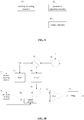
- FIG. 1 schematically illustrates a structural diagram of an ideal PFC circuit in prior art.
- the PFC circuit operates in a continuous conduction mode with a fixed switching frequency, and the PFC circuit is already used in an AC-DC (Alternating Current Direct Current) power supply for many years to reduce a harmonic distortion of a current and increase a power factor in a single-phase power system.
- AC-DC Alternating Current Direct Current
- 101 represents an ideal AC voltage source that powers the entire PFC circuit with a small internal impedance.
- 102, 103, 104, and 105 are power diodes respectively, and the four power diodes form a diode rectifier bridge that rectifies an input alternating current (AC) to a direct current (DC).
- 106 denotes an inductor that stores electrical energy.
- 107 is an electrical switch, the inductor 106 can be charged when the electrical switch 107 is turned off. When the electrical switch 107 is turned on, a current from the inductor 106 is released and flows through a diode 108 to charge a capacitor 109.
- the capacitor 109 acts as a buffer to filter ripples flowing to a load 110.
- PFC circuits must have at least one switch for adjusting the current waveform. Therefore, some PFC circuits place the switch of this function on the rectifier bridge, such as the PFC circuit.
- FIG. 2 schematically illustrates a structural diagram of an ideal PFC circuit in prior art.
- an inductance L is the same as 106 in FIG. 1
- a capacitance C is the same as 109 in FIG. 1 .
- Field effect transistors S D1 and S D2 are used as rectifiers, similar to 102-105 in FIG. 1 , but have a different operating mechanism.
- a voltage of a power supply Vac is the same as a voltage between 101 and 205.
- field effect transistors S D1 and S D2 are switches for rectification, and S 1 and S 2 are configured to control the current, so that a voltage at V S may be taken as a sampling voltage for loop control.
- FIG. 3 schematically illustrates a structural diagram of an equivalent circuit of an actual PFC circuit with a digital control function.
- 201 represents an ideal AC voltage source, but any AC power system is not an ideal AC voltage source because it always has an impedance before it is coupled to an electrical product.
- a resistor 203 with a high resistance and an inductor 202 may cause a high impedance and energy loss. Since the inductor 202 and the resistor 203 are connected in series, the input current becomes high, which causes the voltage to drop in front of a rectifier 205.
- an EMI (Electromagnetic Interference) 204 is an equivalent low pass filter configured to prevent electromagnetic interference from other electrical devices that share the same AC power.
- 205 is a rectification circuit, such as a conventional diode bridge or a synchronous rectifier with an electrical switch that rectifies the input AC to DC.
- 210 is a boost power conversion circuit, in parallel with a load 110 or a load 213, draws a synchronous sinusoidal current from the input voltage source 201 through 202, 203, 204, and 205 with a goal of maintaining a constant voltage at a snubber capacitor 109 or a snubber capacitor 212.
- the actions described above are all performed by a digital controller 206 through complex calculations and algorithms.
- an input current 211 By detecting an input voltage 207 before or after rectification, an input current 211, an output voltage 209, and a driver 206 amplify a Pulse Width Modulation (PWM) signal input from the digital controller 206, and output to the electrical switch 107.
- PWM Pulse Width Modulation
- a current loop filter requires a large number of PID gain parameters to achieve a better sinusoidal input current.
- the existing design works well, and the input current and the input voltage may have the same waveform.
- an oscillating input current waveform is generated. And in some more serious cases, not only the current waveform oscillates, but also a waveform of the input voltage oscillates.
- the input current of the current PFC circuit still has a severe harmonic distortion, and an insufficient phase margin.
- an impedance change of the AC power source can be estimated. Therefore, according to the stability degree of the input voltage of the power factor correction circuit, a current control parameter of the PID or the PI is adjusted correspondingly, and a control signal of the at least one switching circuit is adjusted by using the adjusted control parameter of the PID or the PI to improve the stability degree of the power factor correction circuit, which reduces the oscillation and the harmonic distortion of the input current.
- a power factor correction (PFC) circuit may include: a rectification circuit and at least one switching circuit, wherein the at least one switch circuit is configured to adjust a current in the power factor correction circuit.
- FIG. 4 schematically illustrates a flow diagram of a method for controlling a power factor correction circuit according to an embodiment of the present disclosure. Referring to FIG. 4 , the method is described in detail in steps.
- an input voltage of the PFC circuit is not an ideal sine wave, and a certain fluctuation or oscillation occurs, in other words, the input voltage has a low stability degree.
- the stability degree may have a positive correlation with a frequency and/or an amplitude deviation of the input voltage from a predetermined trend.
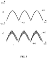
- FIG. 5 schematically illustrates a waveform diagram of an ideal input voltage and a corresponding oscillating input voltage according to an embodiment of the present disclosure.
- a horizontal axis represents time t(s), and a vertical axis represents voltage V(v).
- 401 shows an ideal input voltage waveform, that is, a waveform for the input voltage conforming to the predetermined trend.
- 402 shows an oscillating input voltage waveform, that is, a waveform for the input voltage deviating from the predetermined trend
- 403 and 404 represent zero crossing points.
- an instantaneous value of the input voltage conforming to the predetermined trend is v1
- the instantaneous value of the input voltage deviating from the predetermined trend is v2
- v1 is predetermined
- an amplitude of the input voltage deviating from the predetermined trend is
- a process of detecting the stability degree of the input voltage of the power factor correction circuit may be performed according to a predetermined frequency, and the predetermined frequency may be a fixed value, or may be a value that changes according to a predetermined rule.
- the process of detecting the stability degree of the input voltage of the power factor correction circuit is performed when a predetermined condition is satisfied.
- a predetermined condition for example, the stability degree of the input voltage of the power factor correction circuit that is detected last time is less than a predetermined threshold of the stability degree.
- an impedance of the power supply may not be directly obtained.
- the input voltage of the PFC circuit is oscillated correspondingly. Therefore, by detecting the stability degree of the input voltage of the PFC circuit, the impedance variation of the power supply corresponding thereto may be obtained.
- a corresponding mapping relationship between the current loop control parameter and the stability degree of the input voltage of the PFC circuit may be obtained through experiments. Therefore, according to the stability degree of the PFC circuit, the control parameter of a loop control circuitry currently used (i.e., the control parameter of the PID or the PI) can be adjusted, and the adjusted PID or PI control parameters are obtained.
- control parameter of the PID or the PI includes one or more of a proportional coefficient, an integral coefficient, and a differential coefficient.
- the control parameter may be set to other types by those skilled in the art according to actual needs.
- S33 a voltage loop and/or a current loop are controlled by using the adjusted control parameter of the PID or the PI to adjust a control signal of the at least one switching circuit.
- the voltage loop and/or the current loop are controlled by using the adjusted control parameter of the PID or the PI, to finally implement adjustment of the control signal of the at least one switch circuit.
- the adjusted control parameter of the PID or the PI may be configured to maintain the power factor correction circuit at a predetermined stability degree, which improves the stability degree of the power factor correction circuit and reduces the oscillation and the harmonic distortion of the input current.
- a plurality of methods may be used to detect the stability degree of the input voltage of the power factor correction circuit.
- the input voltage of the power factor correction circuit may be sampled, and a number of times of the input voltage deviating from the predetermined trend by a predetermined value within a predetermined duration may be calculated. Further, according to the number of times of the input voltage deviating from the predetermined trend by the predetermined value within the predetermined duration, the stability degree of the input voltage of the power factor correction circuit is determined finally.
- sampling points for sampling the input voltage of the power factor correction circuit are set to a line that directly or indirectly reflects an alternating voltage change at an input end, to improve sampling accuracy.
- the line that directly or indirectly reflects the change in the alternating voltage change at the input end may include a live wire.
- the live wire may be used as a bus bar in some cases, and the live wire is a position that is not filtered by a capacitor parallel to an output end and directly or indirectly reflects the change in the alternating voltage change at the input end.
- a voltage waveform that is not rectified by the rectification circuit is a sinusoidal alternating voltage, and after rectification, the sinusoidal alternating voltage is converted into a continuous forward half-wave (known as a skull-shaped wave).
- Positions and lines that can detect the two types of the input voltage waveform may be used as sampling points of the voltage. Therefore, sampling is performed on the live line (or bus), a line used as the bus bar, the input end and the output end of the rectification circuit.
- points PI, P2, P3 and P4 may be used as sampling points.
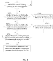
- FIG. 6 schematically illustrates a flow diagram of a method for detecting stability degree of the input voltage of a power factor correction circuit according to an embodiment of the present disclosure.
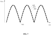
- FIG. 7 schematically illustrates a waveform diagram of an input voltage according to an embodiment of the present disclosure.
- a horizontal axis represents time t(s)
- a vertical axis represents the voltage V(v)
- 601 represents a zero crossing point.
- the method of detecting the stability degree of the input voltage of the power factor correction circuit may include following steps.
- S501 the input voltage of the power factor correction circuit is sampled.
- sampling points like 603 may be selected and the sampling may be performed at predetermined time intervals.
- a current sampling point 603 is defined as a sampling point for the i-th sampling
- a sampling of a sampling point 604 adjacent to the sampling point 603 is defined as the (i+1)-th sampling
- a sampling of a sampling point 604 adjacent to the sampling point 602 is defined as the (i-1)-th sampling.
- V[i] represents a voltage obtained by the i-th sampling
- V[i+1] represents a voltage obtained by the (i+1)-th sampling. For any i-th samplings, it can be determined whether the voltage V[i] obtained by the current sampling is greater than the voltage V[i+1] sampled by the next sampling point.
- V[i] is greater than V[i+1]
- S503 is performed; otherwise, S505 is performed.
- any i-th sampling when it is determined that the voltage V[i] obtained by the current sampling is greater than the voltage V[i+1] sampled by the next sampling point, it is determined that the voltage V[i] obtained by the current sampling is greater than the voltage V[i-1] sampled by the previous sampling point. Therefore, in combination with S502 and S503, it can be determined whether a waveform at the current sampling point 603 is a waveform bulge, that is, whether it is a glitch.
- V[i+1] is greater than V[i+2]
- S504 is performed; otherwise, S505 is performed.
- a counter adds 1;
- the counter is a counter for a number of glitch, the initial value is zero, and the counter is configured to count the waveform bulge, that is, to count the number of glitch.
- S505 it is determined whether the current sampling point is the zero crossing point.
- an instantaneous value of the voltage at the zero crossing point is zero, accordingly, it can be determined whether the current i-th sampling point is the zero crossing point by comparing a voltage of the current sampling point with a voltage of the zero crossing point.
- a waveform between two adjacent zero crossing points is a half-wave, and a corresponding duration is a half period. Therefore, the predetermined duration in some embodiment is a half period, and those skilled in the art may set the predetermined duration to other values according to actual needs.
- the calculator may be reinitialized, the current number of glitch is cleared, and S501 is performed again to start a next loop.
- the current sampling point is not the zero crossing point, which means the predetermined duration has not yet expired, sampling needs to be continued to calculate the total number of glitch in the predetermined duration, and therefore, S501 is continued to be performed.
- that the current control parameter of the PID or the PI is adjusted according to the stability degree of the input voltage of the power factor correction circuit may includes: increasing the control parameter of the PID or the PI when the number of times of the input voltage deviating from the predetermined trend by the predetermined value is less than a second predetermined number threshold within the predetermined duration, wherein the second predetermined number threshold is less than the first predetermined number threshold.
- that the current control parameter of the PID or the PI is adjusted according to the stability degree of the input voltage of the power factor correction circuit may includes: increasing the control parameter of the PID or the PI when the number of times of the input voltage deviating from the predetermined trend by the predetermined value is greater than a first predetermined number threshold within the predetermined duration, which may reduce an oscillation degree of the output current.
- An excessive adjustment may cause that the power factor control circuit does not work, in order to avoid the case, in some embodiments, when the current control parameter of the PID exceeds a predetermined control parameter threshold range of the PID, the current control parameter of the current PID is restricted to the control parameter threshold range of the PID.
- FIG. 8 schematically illustrates a flow diagram of a method for controlling a loop with adjusted control parameters of the PID or the PI according to an embodiment of the present disclosure.
- the adjustment process may be performed as follows.
- S701 it is determined whether the current sampling point is the zero crossing point.
- the instantaneous value of the voltage at the zero crossing point is zero, therefore, it can be determined whether the current i-th sampling point is the zero crossing point by comparing the voltage of the current sampling point with the voltage of the zero crossing point.
- a waveform between two adjacent zero crossing points is a half-wave, and the corresponding duration is a half period. Therefore, the predetermined duration in some embodiment is a half period, and those skilled in the art may set the predetermined duration to other values according to actual needs.
- S702 it is determined whether the number of glitch in the half wave is greater than a first predetermined number threshold.
- S703 may be performed; otherwise, S704 may be performed.
- S704 may be performed after the control parameter of the PID or the PI is decreased.
- S704 it is determined whether the number of glitch in the half wave is less than a second predetermined number threshold.
- the second predetermined number threshold is less than the first predetermined number threshold.
- S705 is performed; otherwise, S706 is performed.
- control parameter of the PID or the PI may be correspondingly increased when the number of glitch in the half wave is less than the second predetermined number threshold.
- step S706 may further be performed after the current control parameter of the PID or the PI is increased.
- S706 it is determined whether the current control parameter PID exceeds the predetermined control parameter threshold range of the PID.
- S707 is performed; otherwise, S701 may be continued to start a next cycle for adjustment.
- the current control parameter of the current PID may be restricted to the control parameter threshold range of the PID, which improves performance of the power factor correction circuit.
- FIG. 9 schematically illustrates a structural diagram of a controller of the power factor correction circuit according to an embodiment of the present disclosure.
- the controller may include: a stability detecting circuitry 81, a parameter adjusting circuitry 82 and a control circuitry 83.
- the stability detecting circuitry 81 is configured to detect the stability degree of the input voltage of the power factor correction circuit. Moreover, the stability degree may be a frequency and/or an amplitude of the input voltage deviating from the predetermined trend.
- the parameter adjusting circuitry 82 is configured to adjust the current control parameter of the PID or the PI according to the stability degree of the input voltage of the power factor correction circuit, wherein the control parameter of the PID or the PI may include one or more of a proportional coefficient, an integral coefficient, and a differential coefficient.
- the control circuitry 83 is configured to control a voltage loop and/or a current loop using the adjusted control parameter of the PID or the PI to adjust a control signal of the at least one switching circuit. Moreover, the adjusted control parameter of the PID or the PI is configured to maintain the power factor correction circuit at a predetermined stability degree, which may avoid the oscillation of the power factor correction circuit due to large variations in the input impedance of the current source.
- control parameters adjusted by the control circuitry 83 are also different.
- the control circuitry 83 may adjust three control parameters corresponding to the PID.
- the control circuitry 83 can may two control parameters corresponding to the PI.
- control parameter of the PID may include at least one of the following: a proportional gain parameter and an integral gain parameter.
- the control circuitry 83 may only adjust the proportional gain parameter and/or the integral gain parameter without adjusting the differential gain parameter.
- control parameter of the PID may include at least one of the following: a proportional gain parameter, an integral gain parameter and a differential gain parameter.
- control circuitry 83 may simultaneously adjust the three control parameters corresponding thereto, so that comprehensiveness of the adjustment may be improved.
- the controller of the power factor correction circuit may further include: a current loop, and the control circuitry 83 may be configured to control the current loop to adjust a control signal of the at least one switching circuit in the power factor correction circuit by using the adjusted control parameter of the PID or the PI.
- FIG. 10 schematically illustrates a structural diagram of a controller of the power factor correction circuit according to an embodiment of the present disclosure.
- the controller may include: a first comparator 91, a reference current generation circuit, a second comparator 95, a current PID loop 96, a pulse width modulator 97, the stability detecting circuitry 81, the parameter adjusting circuitry 82, and the control circuitry 83.
- the first comparator 91 is configured to compare a target output voltage with a current output voltage and obtain a first comparison result.
- the reference current generation circuit is configured to receive a current input voltage and the first comparison result, generate a reference current, and output the reference current to the second comparator 95.
- the second comparator 95 is configured to compare the current input current with the reference current, and output the second comparison result obtained after the comparison to the current PID loop 96.
- the stability detecting circuitry 81 is configured to detect the stability degree of the input voltage of the power factor correction circuit. Moreover, the stability degree may be the frequency and/or the amplitude of the input voltage deviating from the predetermined trend.
- the parameter adjusting circuitry 82 is configured to adjust the current control parameter of the current PID according to the stability degree of the input voltage of the power factor correction circuit, wherein the control parameter may include one or more of a proportional coefficient, an integral coefficient, and a differential coefficient.
- the control circuitry 83 is configured to control the current PID loop 96 by using the adjusted control parameter of the PID to adjust the control signal of the at least one switching circuit, wherein the adjusted control parameter of the PID is configured to maintain the power factor correction circuit at a predetermined stability degree.
- the current PID loop 96 is configured to receive the second comparison result and the adjusted control parameter of the PID, adjust the second comparison result according to the adjusted control parameter of the PID, and output the second adjusted comparison result.
- the pulse width modulator 97 (PWM) is configured to perform a pulse width modulation on the second adjusted comparison result and output the second modulated comparison result as a control signal to the at least one switching circuit of the power factor correction circuit.
- the current PID loop 96 is configured to adjust an input current waveform by receiving a feedback error from the second comparator 95, to calculate duty cycle output from a driver of the pulse width modulator 97 to the power factor correction circuit.
- the driver may be 208.
- the reference current generating circuit may include a mixer 92, a mean square error calculating circuitry 93, and a squaring circuitry 94, wherein the mixer 92 is configured to mix the current input voltage and the first comparison result, the mean square error calculation circuitry 93 is configured to calculate a mean square error of the current input voltage, and the input voltage and the mean square error RMS satisfy the following relationship.
- RMS 2 T ⁇ 0 T / 2 Vin t 2 dt
- T is a period of the voltage waveform.
- the squaring circuitry 94 is configured to receive a result output from the mixer 92 and the mean square error RMS, generate the reference current, and output to the second comparator 95.
- the controller of the power factor correction circuit may further include: a voltage loop, wherein the control circuitry 83 may be configured to control the current loop to adjust a control signal of the at least one switching circuit in the power factor correction circuit by using the adjusted control parameter of the PID or the PI, which improves convenience of the circuit adjustment.
- FIG. 11 schematically illustrates a structural diagram of a controller of the power factor correction circuit according to an embodiment of the present disclosure.
- the controller may include: a first comparator 101, a voltage PID loop 106, a reference current generation circuit, a second comparator 105, a pulse width modulator 107, the stability detecting circuitry 81, the parameter adjusting circuitry 82, and control circuitry 83.
- the first comparator 101 is configured to compare a target output voltage with a current output voltage and obtain a third comparison result and output the third comparison result to the voltage PID loop 106.
- the stability detecting circuitry 81 is configured to receive the current input voltage, and detect the stability degree of the input voltage of the power factor correction circuit.
- the parameter adjusting circuitry 82 is configured to adjust the current control parameter of the current PID according to the stability degree of the current input voltage, wherein the control parameter may include one or more of a proportional coefficient, an integral coefficient, and a differential coefficient.
- the control circuitry 83 is configured to control the current PID loop 106 by using the adjusted control parameter of the PID to adjust the control signal of the at least one switching circuit, wherein the adjusted control parameter of the PID is configured to maintain the power factor correction circuit at a predetermined stability degree.
- the voltage PID loop 106 is configured to receive the third comparison result and the adjusted control parameter of the PID, and adjust the third comparison result according to the adjusted control parameter of the PID.
- the reference current generating circuit is configured to receive the current input voltage and the third adjusted comparison result, generate a reference current, and output the reference current to the second comparator 105.
- the second comparator 105 is configured to compare the current input current with the reference current and output a fourth comparison result obtained after the comparison to the pulse width modulator 107.
- the pulse width modulator 107 is configured to perform a pulse width modulation on the fourth adjusted comparison result and output the fourth modulated comparison result as a control signal to at least one switch circuit of the power factor correction circuit.
- the reference current generating circuit may include a mixer 102, a mean square error calculating circuitry 103, and a squaring circuitry 104.
- the controller of the power factor correction circuit may further include: a current loop and a voltage loop.
- control circuitry 83 may be configured to preferentially control the current loop using the adjusted control parameter of the PID or the PI to adjust a control signal of at least one switch circuit of the power factor correction circuit.
- a reason is that a purpose of the power factor correction circuit is to adjust the voltage and the current to be in the same phase, and the current is the adjustment target of the power control circuit. Therefore, adjusting the PID parameter of the current loop may effectively affect sensitivity of the circuit to an electrical environment. In combination with the above embodiments, a correlation between the PID parameter of the current loop and the number of glitch in the predetermined duration is great.
- FIG. 12 schematically illustrates a structural diagram of a controller of the power factor correction circuit according to an embodiment of the present disclosure.
- the controller may include: a first comparator 111, a reference current generation circuit, a second comparator 115, a current PID loop 116, a voltage PID loop 118, a pulse width modulator 117, the stability detecting circuitry 81, the parameter adjusting circuitry 82, and the control circuitry 83.
- the first comparator 111 is configured to compare a target output voltage with a current output voltage and obtain a first comparison result.
- the voltage PID loop 118 is configured to receive the first comparison result and adjust the first comparison result.
- the reference current generation circuit is configured to receive the current input voltage and the first comparison result adjusted by the voltage PID loop 118, generate a reference current, and output to the second comparator 115.
- the second comparator 115 is configured to compare the current input current with the reference current, and output a second comparison result obtained after the comparison to the current PID loop 116.
- the stability detecting circuitry 81 is configured to detect the stability degree of the input voltage of the power factor correction circuit. Moreover, the stability degree may be the frequency and/or the amplitude of the input voltage deviating from the predetermined trend.
- the parameter adjusting circuitry 82 is configured to adjust the current control parameter of the current PID according to the stability degree of the input voltage of the power factor correction circuit, wherein the control parameter may include one or more of a proportional coefficient, an integral coefficient, and a differential coefficient.
- the current PID loop 116 is configured to receive the second comparison result and the adjusted control parameter of the PID, adjust the second comparison result according to the adjusted control parameter of the PID, and output the second adjusted comparison result.
- the pulse width modulator 117 is configured to perform a pulse width modulation on the second adjusted comparison result and output the second modulated comparison result as a control signal to the at least one switching circuit of the power factor correction circuit.
- the reference current generating circuit may be configured by referring to the reference current generating circuit in FIG. 12 , and may include a mixer 112, a mean square error calculating circuitry 113, and a squaring circuitry 114, whose function is not described in detail herein.
- the controller of the power factor correction circuit may further include: a current loop and a voltage loop.
- the control circuitry 83 may be configured to preferentially control the voltage loop by using the adjusted control parameter of the PID or the PI to adjust a control signal of at least one switch circuit of the power factor correction circuit, which improves convenience of circuit adjustment.
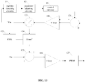
- FIG. 13 schematically illustrates a structural diagram of a controller of the power factor correction circuit according to an embodiment of the present disclosure.
- the controller may include: a first comparator 121, a reference current generation circuit, a second comparator 125, a current PID loop 126, a voltage PID loop 128, a pulse width modulator 127, the stability detecting circuitry 81, the parameter adjusting circuitry 82, and the control circuitry 83.
- the first comparator 121 is configured to compare a target output voltage with a current output voltage and obtain a first comparison result.
- the stability detecting circuitry 81 is configured to receive the current input voltage, and detect the stability degree of the input voltage.
- the parameter adjusting circuitry 82 is configured to adjust the current control parameter of the current PID according to the stability degree of the current input voltage, wherein the control parameter may include one or more of a proportional coefficient, an integral coefficient, and a differential coefficient.
- the control circuitry 83 is configured to control the current PID loop 128 by using the adjusted control parameter of the PID to adjust the control signal of the at least one switching circuit, wherein the adjusted control parameter of the PID is configured to maintain the power factor correction circuit at a predetermined stability degree.
- the voltage PID loop 128 is configured to receive the third comparison result and the adjusted control parameter of the PID, and adjust the third comparison result according to the adjusted control parameter of the PID.
- the reference current generating circuit is configured to receive the current input voltage and the third adjusted comparison result, generate a reference current, and output the reference current to the second comparator 125.
- the second comparator 125 is configured to compare the current input current with the reference current and output a fourth comparison result obtained after the comparison to the current PID loop 126.
- the current PID loop 126 is configured to adjust the fourth comparison result and output the fourth adjusted comparison result.
- the pulse width modulator 127 (PWM) is configured to perform a pulse width modulation on the fourth adjusted comparison result, and output the fourth modulated comparison result as a control signal to the at least one switching circuit of the power factor correction circuit.
- the reference current generating circuit may include a mixer 122, a mean square error calculating circuitry 123, and a squaring circuitry 124.
- the controller of the power factor correction circuit may further include: a current loop and a voltage loop.
- the control circuitry 83 may be control to simultaneously control the current loop and the voltage loop by using the adjusted control parameter of the PID or the PI to adjust a control signal of the at least one switch circuit of the power factor correction circuit, which improves a effect of the circuit adjustment.
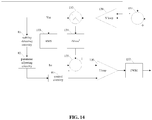
- FIG. 14 schematically illustrates a structural diagram of a controller of the power factor correction circuit according to an embodiment of the present disclosure.
- the controller may include: a first comparator 131, a reference current generation circuit, a second comparator 135, a current PID loop 136, a voltage PID loop 138, a pulse width modulator 137, the stability detecting circuitry 81, the parameter adjusting circuitry 82, and the control circuitry 83.
- the first comparator 131 is configured to compare a target output voltage with a current output voltage and obtain a first comparison result.
- the stability detecting circuitry 81 is configured to receive the current input voltage and detect the stability degree of the input voltage.
- the parameter adjusting circuitry 82 is configured to adjust the current control parameter of the current PID according to the stability degree of the current input voltage, wherein the control parameter may include one or more of a proportional coefficient, an integral coefficient, and a differential coefficient, and include a voltage PID control parameter and a current PID control parameter.
- the control circuitry 83 is configured to control the voltage PID loop 138 by using the adjusted voltage PID control parameter and control the current PID loop 136 by using the adjusted current PID control parameter, to adjust a control signal of at least one switching circuit of the power factor correction circuit.
- the voltage PID control parameter and the current PID control parameter are jointly configured to maintain the power factor correction circuit at a predetermined stability degree.
- the voltage PID loop 138 is configured to receive the third comparison result and the adjusted voltage PID control parameter, and adjust the third comparison result according to the adjusted control voltage PID control parameter.
- the reference current generating circuit is configured to receive the current input voltage and the third adjusted comparison result, generate a reference current, and output the reference current to the first comparator 135.
- the first comparator 135 is configured to compare the current input current with the reference circuit, and output the fourth comparison result obtained after the comparison to the current PID loop 136.
- the current PID loop 136 is configured to receive the fourth comparison result and the adjusted current PID control parameter, and adjust the fourth comparison result according to the adjusted current PID control parameter, and output the fourth comparison result after the adjustment.
- the pulse width modulator 137 is configured to perform a pulse width modulation on the fourth adjusted comparison result, and output the fourth adjusted comparison result as a control signal to the at least one switching circuit of the power factor correction circuit.
- the reference current generating circuit may include a mixer 132, a mean square error calculating circuitry 133, and a squaring circuitry 134.
- embodiments of the present disclosure further provide a system for a power factor correction circuit, wherein the system of the power factor correction circuit may include: anyone of the controller of the power factor correction circuit mentioned above, a power factor correction circuit, a power supply and a load.
- the power factor correction circuit is configured to correct a power factor of the power supply.
- the power supply is coupled to an input end of the power factor correction circuit.
- the load is coupled to an output end of the power factor correction circuit.
Landscapes
- Engineering & Computer Science (AREA)
- Power Engineering (AREA)
- Physics & Mathematics (AREA)
- General Physics & Mathematics (AREA)
- Automation & Control Theory (AREA)
- Rectifiers (AREA)
- Dc-Dc Converters (AREA)
Abstract
Description
- The present disclosure relates to an integrated circuit field, and more particularly, to a method for controlling a power factor correction circuit, a controller for the power factor correction circuit and a system for the power factor correction circuit.
- A power factor is a parameter for measuring a power efficiency of an electrical device, and a low power factor represents a low power efficiency. In electrical engineering, a power factor of an alternating current power system is defined as a ratio of an active power flowing into a load to an apparent power in a circuit, and it is a dimensionless number in the closed interval from -1 to 1. The power factor less than 1 means that a voltage waveform and a current waveform are out of phase, thereby reducing an instantaneous product of the two waveforms. Actual power consumption is an ability of a circuit to execute operations at a specific time point. Apparent power is a product of a current and a voltage in the circuit. Since the energy is stored in the load and returned to a power supply, or the non-linear load distorts the waveform of the current drawn from the power supply, the apparent power is greater than the actual power. When a device (usually a load) generates power, a negative power factor is generated and flows to a generator which is generally regarded as a power supply. In an electrical power system, a load with a low power factor absorbs more current while transmitting a same useful power compared with a load with a high power factor. Higher currents increase energy losses in a power distribution system and require larger wires and other equipments. Due to high cost of equipments and wasted energy, power companies typically charge higher costs to industrial or commercial customers with lower power factors.
- Power Factor Correction (PFC) is a technique to increase the power factor of the electrical device. Linear loads (e.g., induction motors) with low power factor may be corrected through a passive capacitor or an inductive network. A nonlinear load (e.g., a rectifier) may distort the current drawn from the system. In this case, active or passive power factor correction may be configured to cancel a distortion and increase the power factor. The device used to correct the power factor may be disposed in a central substation, distributed in a power distribution system, or set into power consuming equipments.
- However, current nonlinear PID (proportion, integral, differential) control can only handle a small range of input voltages and impedances. When an input voltage of the AC (alternating current) power source is high or the impedance range is wide, it is easy to cause an oscillation to the input current and the input voltage.
- At present, there are complex equations to calculate the control parameters, and the calculated control parameters are configured to control a PFC circuit. These methods may solve most of the related oscillation problems. However, the problem of serious harmonic distortion and insufficient phase margin of the input current still remains unsolved.
- Embodiments of the present disclosure provide a method to reduce an oscillation and a harmonic distortion of an input current.
- Embodiments of the present disclosure may provide a method for controlling a power factor correction circuit, wherein the power factor correction circuit includes: a rectification circuit and at least one switching circuit, wherein the at least one switching circuit is configured to adjust a current in the power factor correction circuit, and the method includes: detecting a stability degree of an input voltage of the power factor correction circuit, wherein the stability degree is a frequency and/or an amplitude deviation of the input voltage from a predetermined trend; adjusting a current control parameter of PID (proportion, integral, differential) or PI (proportion, integral) according to the stability degree of the input voltage of the power factor correction circuit, wherein the control parameter of the PID or the PI includes one or more of a proportional coefficient, an integral coefficient, and a differential coefficient; and controlling a voltage loop and/or a current loop using the adjusted control parameter of the PID or the PI to adjust a control signal of the at least one switching circuit, wherein the adjusted control parameter of the PID or the PI is configured to maintain the power factor correction circuit at a predetermined stability degree.
- In some embodiments, the detecting a stability degree of an input voltage of the power factor correction circuit includes: sampling the input voltage of the power factor correction circuit; calculating a number of times of the input voltage deviating from the predetermined trend by a predetermined value within a predetermined duration; and determining a stability degree of the input voltage of the power factor correction circuit according to the number of times of the input voltage deviating from the predetermined trend by the predetermined value within the predetermined duration.
- In some embodiments, sampling points for sampling the input voltage of the power factor correction circuit are set to a line that directly or indirectly reflects an alternating voltage change at an input end.
- In some embodiments, the adjusting a current control parameter of PID or PI according to the stability degree of the input voltage of the power factor correction circuit includes: decreasing the control parameter of the PID or the PI when the number of times of the input voltage deviating from the predetermined trend by the predetermined value is greater than a first predetermined number threshold within the predetermined duration.
- In some embodiments, the adjusting a current control parameter of PID or PI according to the stability degree of the input voltage of the power factor correction circuit includes: increasing the control parameter of the PID or the PI when the number of times of the input voltage deviating from the predetermined trend by the predetermined value is less than a second predetermined number threshold within the predetermined duration, wherein the second predetermined number threshold is less than the first predetermined number threshold.
- In some embodiments, the method further includes: when the current control parameter of the PID exceeds a predetermined control parameter threshold range of the PID, restricting the current control parameter of the current PID to the control parameter threshold range of the PID.
- In some embodiments, the detecting stability degree of the input voltage of the power factor correction circuit is performed according to a predetermined frequency.
- Embodiments of the present disclosure may provide a controller for a power factor correction circuit, including: a stability detecting circuitry, configured to a stability degree of an input voltage of the power factor correction circuit, wherein the stability degree is a frequency and/or an amplitude deviation of the input voltage from a predetermined trend; a parameter adjusting circuitry, configured to adjusting a current control parameter of PID or PI according to the stability degree of the input voltage of the power factor correction circuit, wherein the control parameter of the PID or the PI includes one or more of a proportional coefficient, an integral coefficient, and a differential coefficient; and a control circuitry, configured to control a voltage loop and/or a current loop using the adjusted control parameter of the PID or the PI to adjust a control signal of the at least one switching circuit, wherein the adjusted control parameter of the PID or the PI is configured to maintain the power factor correction circuit at a predetermined stability degree.
- In some embodiments, the control parameter of the PID includes at least one of the following: a proportional gain parameter and an integral gain parameter.
- In some embodiments, the control parameter of the PID includes at least one of the following: a proportional gain parameter, an integral gain parameter and a differential gain parameter.
- In some embodiments, the controller further includes: a current loop, wherein the control circuitry is configured to control the current loop to adjust a control signal of the at least one switching circuit in the power factor correction circuit by using the adjusted control parameter of the PID or the PI.
- In some embodiments, the controller further includes: a current loop and a voltage loop, wherein the control circuitry is configured to control the current loop to adjust a control signal of the at least one switching circuit in the power factor correction circuit by using the adjusted control parameter of the PID or the PI.
- Embodiments of the present disclosure may provide a system for a power factor correction circuit, including: a controller for the power factor correction circuit, a power factor correction circuit, a power supply and a load; wherein the power factor correction circuit is configured to correct a power factor of the power supply; the power supply is coupled to an input end of the power factor correction circuit; and the load is coupled to an output end of the power factor correction circuit.
- Embodiments of the present disclosure have the following benefits.
- In embodiments of present disclosure, without knowledge of an impedance value of the AC power supply, by detecting stability degree of the input voltage of the power factor correction circuit, an impedance change of the AC power source can be estimated. According to the stability degree of the input voltage of the power factor correction circuit, a current control parameter of the PID or the PI is adjusted correspondingly, and a control signal of at least one switching circuit is adjusted by using the adjusted control parameter of the PID or the PI to improve the stability degree of the power factor correction circuit, which reduces the oscillation and the harmonic distortion of the input current.
-
-
FIG. 1 schematically illustrates a structural diagram of an ideal PFC circuit in prior art; -
FIG. 2 schematically illustrates a structural diagram of an ideal PFC circuit in prior art; -
FIG. 3 schematically illustrates a structural diagram of an equivalent circuit of an actual PFC circuit in prior art; -
FIG. 4 schematically illustrates a flow diagram of a method for controlling a power factor correction circuit according to an embodiment of the present disclosure; -
FIG. 5 schematically illustrates a waveform diagram of an ideal input voltage and a corresponding oscillating input voltage according to an embodiment of the present disclosure; -
FIG. 6 schematically illustrates a flow diagram of a method for detecting stability degree of the input voltage of a power factor correction circuit according to an embodiment of the present disclosure; -
FIG. 7 schematically illustrates a waveform diagram of an input voltage according to an embodiment of the present disclosure; -
FIG. 8 schematically illustrates a flow diagram of a method for controlling a loop with adjusted control parameters of the PID or the PI according to an embodiment of the present disclosure; -
FIG. 9 schematically illustrates a structural diagram of a controller of the power factor correction circuit according to an embodiment of the present disclosure; -
FIG. 10 schematically illustrates a structural diagram of a controller of the power factor correction circuit according to an embodiment of the present disclosure; -
FIG. 11 schematically illustrates a structural diagram of a controller of the power factor correction circuit according to an embodiment of the present disclosure; -
FIG. 12 schematically illustrates a structural diagram of a controller of the power factor correction circuit according to an embodiment of the present disclosure; -
FIG. 13 schematically illustrates a structural diagram of a controller of the power factor correction circuit according to an embodiment of the present disclosure; and -
FIG. 14 schematically illustrates a structural diagram of a controller of the power factor correction circuit according to an embodiment of the present disclosure. - For facilitating explanation and understanding,
FIG. 1 schematically illustrates a structural diagram of an ideal PFC circuit in prior art. The PFC circuit operates in a continuous conduction mode with a fixed switching frequency, and the PFC circuit is already used in an AC-DC (Alternating Current Direct Current) power supply for many years to reduce a harmonic distortion of a current and increase a power factor in a single-phase power system. - As shown in
FIG. 1 , 101 represents an ideal AC voltage source that powers the entire PFC circuit with a small internal impedance. 102, 103, 104, and 105 are power diodes respectively, and the four power diodes form a diode rectifier bridge that rectifies an input alternating current (AC) to a direct current (DC). 106 denotes an inductor that stores electrical energy. 107 is an electrical switch, theinductor 106 can be charged when theelectrical switch 107 is turned off. When theelectrical switch 107 is turned on, a current from theinductor 106 is released and flows through adiode 108 to charge acapacitor 109. Thecapacitor 109 acts as a buffer to filter ripples flowing to aload 110. - It should be noted that generally all PFC circuits must have at least one switch for adjusting the current waveform. Therefore, some PFC circuits place the switch of this function on the rectifier bridge, such as the PFC circuit.
- For convenience of explanation,
FIG. 2 schematically illustrates a structural diagram of an ideal PFC circuit in prior art. As shown inFIG. 2 , an inductance L is the same as 106 inFIG. 1 , and a capacitance C is the same as 109 inFIG. 1 . Field effect transistors SD1 and SD2 are used as rectifiers, similar to 102-105 inFIG. 1 , but have a different operating mechanism. A voltage of a power supply Vac is the same as a voltage between 101 and 205. InFIG. 2 , field effect transistors SD1 and SD2 are switches for rectification, and S1 and S2 are configured to control the current, so that a voltage at VS may be taken as a sampling voltage for loop control. - Correspondingly,
FIG. 3 schematically illustrates a structural diagram of an equivalent circuit of an actual PFC circuit with a digital control function. - As shown in
Figure 3 , 201 represents an ideal AC voltage source, but any AC power system is not an ideal AC voltage source because it always has an impedance before it is coupled to an electrical product. When a length of the connecting line becomes longer or the electrical product is supplied through an isolation transformer, a resistor 203 with a high resistance and an inductor 202 may cause a high impedance and energy loss. Since the inductor 202 and the resistor 203 are connected in series, the input current becomes high, which causes the voltage to drop in front of a rectifier 205. Since a boost circuit 210 may generate switching noise and a power electronic switch 107 (e.g., GaN FET, MOSFET, IGBT, BJT) in 210 has a fast switching action, an EMI (Electromagnetic Interference) 204 is an equivalent low pass filter configured to prevent electromagnetic interference from other electrical devices that share the same AC power. - 205 is a rectification circuit, such as a conventional diode bridge or a synchronous rectifier with an electrical switch that rectifies the input AC to DC. 210 is a boost power conversion circuit, in parallel with a
load 110 or a load 213, draws a synchronous sinusoidal current from the input voltage source 201 through 202, 203, 204, and 205 with a goal of maintaining a constant voltage at asnubber capacitor 109 or a snubber capacitor 212. The actions described above are all performed by a digital controller 206 through complex calculations and algorithms. By detecting an input voltage 207 before or after rectification, an input current 211, an output voltage 209, and a driver 206 amplify a Pulse Width Modulation (PWM) signal input from the digital controller 206, and output to theelectrical switch 107. - Due to some high requirements for standard iTHD or the power factor, a current loop filter requires a large number of PID gain parameters to achieve a better sinusoidal input current. However, in a case where the impedance of the AC power source is low, the existing design works well, and the input current and the input voltage may have the same waveform. However, for high impedance AC power supplies with the same current loop filter gain, an oscillating input current waveform is generated. And in some more serious cases, not only the current waveform oscillates, but also a waveform of the input voltage oscillates.
- In summary, the input current of the current PFC circuit still has a severe harmonic distortion, and an insufficient phase margin.
- In embodiments of present disclosure, under a premise that an impedance value of the AC power supply is unknown, by detecting stability degree of the input voltage of the power factor correction circuit, an impedance change of the AC power source can be estimated. Therefore, according to the stability degree of the input voltage of the power factor correction circuit, a current control parameter of the PID or the PI is adjusted correspondingly, and a control signal of the at least one switching circuit is adjusted by using the adjusted control parameter of the PID or the PI to improve the stability degree of the power factor correction circuit, which reduces the oscillation and the harmonic distortion of the input current.
- In order that the above objects, characteristics and advantages of the present disclosure become more apparent, embodiments of the present disclosure are described in detail with reference to the drawings.
- In some embodiments, a power factor correction (PFC) circuit may include: a rectification circuit and at least one switching circuit, wherein the at least one switch circuit is configured to adjust a current in the power factor correction circuit. Correspondingly,
FIG. 4 schematically illustrates a flow diagram of a method for controlling a power factor correction circuit according to an embodiment of the present disclosure. Referring toFIG. 4 , the method is described in detail in steps. - S31: a stability degree of an input voltage of the power factor correction circuit is detected.
- It should be noted that, due to factors like changes in an input impedance of a power supply, an input voltage of the PFC circuit is not an ideal sine wave, and a certain fluctuation or oscillation occurs, in other words, the input voltage has a low stability degree.
- In some embodiments, the stability degree may have a positive correlation with a frequency and/or an amplitude deviation of the input voltage from a predetermined trend.
- For example,
FIG. 5 schematically illustrates a waveform diagram of an ideal input voltage and a corresponding oscillating input voltage according to an embodiment of the present disclosure. A horizontal axis represents time t(s), and a vertical axis represents voltage V(v). 401 shows an ideal input voltage waveform, that is, a waveform for the input voltage conforming to the predetermined trend. 402 shows an oscillating input voltage waveform, that is, a waveform for the input voltage deviating from the predetermined trend, and 403 and 404 represent zero crossing points. Specifically, at time t, an instantaneous value of the input voltage conforming to the predetermined trend is v1, and the instantaneous value of the input voltage deviating from the predetermined trend is v2, v1 is predetermined, and an amplitude of the input voltage deviating from the predetermined trend is |v1- v2|. - In some embodiment of the present disclosure, for ease of implementation, a process of detecting the stability degree of the input voltage of the power factor correction circuit may be performed according to a predetermined frequency, and the predetermined frequency may be a fixed value, or may be a value that changes according to a predetermined rule.
- In some embodiment of the present disclosure, in order to save resources, the process of detecting the stability degree of the input voltage of the power factor correction circuit is performed when a predetermined condition is satisfied. Those skilled in the art may set the predetermined condition according to actual needs, for example, the stability degree of the input voltage of the power factor correction circuit that is detected last time is less than a predetermined threshold of the stability degree.
- S32: a current control parameter of PID or PI is adjusted according to the stability degree of the input voltage of the power factor correction circuit.
- It should be noted that, because the actual application is complicated and has many uncontrollable factors, an impedance of the power supply may not be directly obtained. However, as described in the background and above, if an impedance variation of the power supply is wide, the input voltage of the PFC circuit is oscillated correspondingly. Therefore, by detecting the stability degree of the input voltage of the PFC circuit, the impedance variation of the power supply corresponding thereto may be obtained.
- Moreover, in some embodiment, a corresponding mapping relationship between the current loop control parameter and the stability degree of the input voltage of the PFC circuit may be obtained through experiments. Therefore, according to the stability degree of the PFC circuit, the control parameter of a loop control circuitry currently used (i.e., the control parameter of the PID or the PI) can be adjusted, and the adjusted PID or PI control parameters are obtained.
- Specifically, the control parameter of the PID or the PI includes one or more of a proportional coefficient, an integral coefficient, and a differential coefficient. The control parameter may be set to other types by those skilled in the art according to actual needs.
- S33: a voltage loop and/or a current loop are controlled by using the adjusted control parameter of the PID or the PI to adjust a control signal of the at least one switching circuit.
- In some embodiments, according to a structural setting of the current PFC circuit, the voltage loop and/or the current loop are controlled by using the adjusted control parameter of the PID or the PI, to finally implement adjustment of the control signal of the at least one switch circuit.
- In some embodiments, the adjusted control parameter of the PID or the PI may be configured to maintain the power factor correction circuit at a predetermined stability degree, which improves the stability degree of the power factor correction circuit and reduces the oscillation and the harmonic distortion of the input current.
- It should be noted that, in some embodiments, a plurality of methods may be used to detect the stability degree of the input voltage of the power factor correction circuit. For example, the input voltage of the power factor correction circuit may be sampled, and a number of times of the input voltage deviating from the predetermined trend by a predetermined value within a predetermined duration may be calculated. Further, according to the number of times of the input voltage deviating from the predetermined trend by the predetermined value within the predetermined duration, the stability degree of the input voltage of the power factor correction circuit is determined finally.
- In some embodiments, sampling points for sampling the input voltage of the power factor correction circuit are set to a line that directly or indirectly reflects an alternating voltage change at an input end, to improve sampling accuracy.
- In particular, the line that directly or indirectly reflects the change in the alternating voltage change at the input end may include a live wire. Moreover, it should be noted that the live wire may be used as a bus bar in some cases, and the live wire is a position that is not filtered by a capacitor parallel to an output end and directly or indirectly reflects the change in the alternating voltage change at the input end. Specifically, a voltage waveform that is not rectified by the rectification circuit is a sinusoidal alternating voltage, and after rectification, the sinusoidal alternating voltage is converted into a continuous forward half-wave (known as a skull-shaped wave). Positions and lines that can detect the two types of the input voltage waveform may be used as sampling points of the voltage. Therefore, sampling is performed on the live line (or bus), a line used as the bus bar, the input end and the output end of the rectification circuit.
- Referring to
FIG. 3 , points PI, P2, P3 and P4 may be used as sampling points. - For ease of explanation and understanding of the method for detecting the stability degree of the input voltage of the power factor correction circuit,
FIG. 6 schematically illustrates a flow diagram of a method for detecting stability degree of the input voltage of a power factor correction circuit according to an embodiment of the present disclosure. Correspondingly,FIG. 7 schematically illustrates a waveform diagram of an input voltage according to an embodiment of the present disclosure. A horizontal axis represents time t(s), a vertical axis represents the voltage V(v), and 601 represents a zero crossing point. Referring toFIG. 6 andFIG. 7 , the method of detecting the stability degree of the input voltage of the power factor correction circuit may include following steps. - S501: the input voltage of the power factor correction circuit is sampled.
- For example, for a voltage waveform 60 shown in
FIG. 7 , sampling points like 603 may be selected and the sampling may be performed at predetermined time intervals. Moreover, if acurrent sampling point 603 is defined as a sampling point for the i-th sampling, a sampling of asampling point 604 adjacent to thesampling point 603 is defined as the (i+1)-th sampling, and a sampling of asampling point 604 adjacent to thesampling point 602 is defined as the (i-1)-th sampling. - S502: it is determined whether V[i] is greater than V[i+1].
- In some embodiments, V[i] represents a voltage obtained by the i-th sampling, and V[i+1] represents a voltage obtained by the (i+1)-th sampling. For any i-th samplings, it can be determined whether the voltage V[i] obtained by the current sampling is greater than the voltage V[i+1] sampled by the next sampling point.
- If V[i] is greater than V[i+1], S503 is performed; otherwise, S505 is performed.
- S503:it is determined whether V[i] is greater than V[i-1].
- In some embodiments, for any i-th sampling, when it is determined that the voltage V[i] obtained by the current sampling is greater than the voltage V[i+1] sampled by the next sampling point, it is determined that the voltage V[i] obtained by the current sampling is greater than the voltage V[i-1] sampled by the previous sampling point. Therefore, in combination with S502 and S503, it can be determined whether a waveform at the
current sampling point 603 is a waveform bulge, that is, whether it is a glitch. - If V[i+1] is greater than V[i+2], S504 is performed; otherwise, S505 is performed.
- S504: a counter adds 1;
In embodiments, the counter is a counter for a number of glitch, the initial value is zero, and the counter is configured to count the waveform bulge, that is, to count the number of glitch. - S505: it is determined whether the current sampling point is the zero crossing point.
- In some embodiments, an instantaneous value of the voltage at the zero crossing point is zero, accordingly, it can be determined whether the current i-th sampling point is the zero crossing point by comparing a voltage of the current sampling point with a voltage of the zero crossing point. Moreover, a waveform between two adjacent zero crossing points is a half-wave, and a corresponding duration is a half period. Therefore, the predetermined duration in some embodiment is a half period, and those skilled in the art may set the predetermined duration to other values according to actual needs.
- If the current sampling point is the zero crossing point, S506 is performed; otherwise, S501 is performed.
- S506: the counter is reinitialized.
- In some embodiments, when the current sampling point is the zero crossing point, which means the predetermined duration has expired, the calculator may be reinitialized, the current number of glitch is cleared, and S501 is performed again to start a next loop. When the current sampling point is not the zero crossing point, which means the predetermined duration has not yet expired, sampling needs to be continued to calculate the total number of glitch in the predetermined duration, and therefore, S501 is continued to be performed.
- In order to improve the stability degree of the output current, in some embodiments, that the current control parameter of the PID or the PI is adjusted according to the stability degree of the input voltage of the power factor correction circuit may includes: increasing the control parameter of the PID or the PI when the number of times of the input voltage deviating from the predetermined trend by the predetermined value is less than a second predetermined number threshold within the predetermined duration, wherein the second predetermined number threshold is less than the first predetermined number threshold.
- In some embodiments, that the current control parameter of the PID or the PI is adjusted according to the stability degree of the input voltage of the power factor correction circuit may includes: increasing the control parameter of the PID or the PI when the number of times of the input voltage deviating from the predetermined trend by the predetermined value is greater than a first predetermined number threshold within the predetermined duration, which may reduce an oscillation degree of the output current.
- An excessive adjustment may cause that the power factor control circuit does not work, in order to avoid the case, in some embodiments, when the current control parameter of the PID exceeds a predetermined control parameter threshold range of the PID, the current control parameter of the current PID is restricted to the control parameter threshold range of the PID.
- For ease of understanding and implementation of the present disclosure,
FIG. 8 schematically illustrates a flow diagram of a method for controlling a loop with adjusted control parameters of the PID or the PI according to an embodiment of the present disclosure. As shown inFIG. 8 , the adjustment process may be performed as follows. - S701: it is determined whether the current sampling point is the zero crossing point.
- Similar to S505, the instantaneous value of the voltage at the zero crossing point is zero, therefore, it can be determined whether the current i-th sampling point is the zero crossing point by comparing the voltage of the current sampling point with the voltage of the zero crossing point. Moreover, a waveform between two adjacent zero crossing points is a half-wave, and the corresponding duration is a half period. Therefore, the predetermined duration in some embodiment is a half period, and those skilled in the art may set the predetermined duration to other values according to actual needs.
- If the current sampling point is the zero crossing point, S702 is performed; otherwise, S701 is repeated.
- S702: it is determined whether the number of glitch in the half wave is greater than a first predetermined number threshold.
- In order to adjust the output current in time to improve the stability, in some embodiments, it can be determined whether the number of glitch in the half wave is greater than a first predetermined number threshold. When the number of glitch in the half wave is greater than the first predetermined number threshold, S703 may be performed; otherwise, S704 may be performed.
- S703: the control parameter of the PID or the PI is decreased.
- In some embodiments, after the control parameter of the PID or the PI is decreased, S704 may be performed.
- S704: it is determined whether the number of glitch in the half wave is less than a second predetermined number threshold.
- It should be noted that the second predetermined number threshold is less than the first predetermined number threshold. In some embodiments, in order to avoid a low operating performance of the power factor amplifying circuit caused by the number of glitch in the half wave being too small, it is continued to determine whether the number of glitch in the half wave is less than a second predetermined number threshold. When the number of glitch in the half wave is less than the second predetermined number threshold, S705 is performed; otherwise, S706 is performed.
- S705: the control parameter of the PID or the PI is increased.
- In some embodiments, In order to improve the stability of the output current, the control parameter of the PID or the PI may be correspondingly increased when the number of glitch in the half wave is less than the second predetermined number threshold. In some embodiment of the present disclosure, after the current control parameter of the PID or the PI is increased, step S706 may further be performed.
- S706: it is determined whether the current control parameter PID exceeds the predetermined control parameter threshold range of the PID.
- If it is determined that the current control parameter PID exceeds the predetermined control parameter threshold range of the PID, S707 is performed; otherwise, S701 may be continued to start a next cycle for adjustment.
- S707: the current control parameter of the current PID is restricted to the control parameter threshold range of the PID.
- In some embodiments, the current control parameter of the current PID may be restricted to the control parameter threshold range of the PID, which improves performance of the power factor correction circuit.
- In order to enable those skilled in the art to better understand and implement the present disclosure,
FIG. 9 schematically illustrates a structural diagram of a controller of the power factor correction circuit according to an embodiment of the present disclosure. As shown inFIG. 9 , the controller may include: astability detecting circuitry 81, aparameter adjusting circuitry 82 and acontrol circuitry 83. - The
stability detecting circuitry 81 is configured to detect the stability degree of the input voltage of the power factor correction circuit. Moreover, the stability degree may be a frequency and/or an amplitude of the input voltage deviating from the predetermined trend. - The
parameter adjusting circuitry 82 is configured to adjust the current control parameter of the PID or the PI according to the stability degree of the input voltage of the power factor correction circuit, wherein the control parameter of the PID or the PI may include one or more of a proportional coefficient, an integral coefficient, and a differential coefficient. - The
control circuitry 83 is configured to control a voltage loop and/or a current loop using the adjusted control parameter of the PID or the PI to adjust a control signal of the at least one switching circuit. Moreover, the adjusted control parameter of the PID or the PI is configured to maintain the power factor correction circuit at a predetermined stability degree, which may avoid the oscillation of the power factor correction circuit due to large variations in the input impedance of the current source. - It should be noted that, according to different structures of a feedback circuit used by the power factor correction circuit, control parameters adjusted by the
control circuitry 83 are also different. For example, when the feedback circuit used by the power factor correction circuit is a PID circuit, thecontrol circuitry 83 may adjust three control parameters corresponding to the PID. For another example, if the feedback circuit used by the power factor correction circuit is a PI circuit, thecontrol circuitry 83 can may two control parameters corresponding to the PI. - Different control parameters have different sensitivity and adjustment effects. Specifically, the proportional gain parameter and the integral gain parameter are relatively easily adjusted, and have weak side effects. Therefore, in order to improve the adjustment effect, in some embodiment of the present disclosure, the control parameter of the PID may include at least one of the following: a proportional gain parameter and an integral gain parameter. In other words, the
control circuitry 83 may only adjust the proportional gain parameter and/or the integral gain parameter without adjusting the differential gain parameter. - In some embodiment, the control parameter of the PID may include at least one of the following: a proportional gain parameter, an integral gain parameter and a differential gain parameter. In other words, the
control circuitry 83 may simultaneously adjust the three control parameters corresponding thereto, so that comprehensiveness of the adjustment may be improved. - It should be noted that structures of the controller may be different according to the loop setting, and correspondingly, the adjusted objects may also be different. In some embodiment of the present disclosure, in order to accurately control a cyclic feedback of the current, the controller of the power factor correction circuit may further include: a current loop, and the
control circuitry 83 may be configured to control the current loop to adjust a control signal of the at least one switching circuit in the power factor correction circuit by using the adjusted control parameter of the PID or the PI. - For ease of understanding,
FIG. 10 schematically illustrates a structural diagram of a controller of the power factor correction circuit according to an embodiment of the present disclosure. As shown inFIG. 10 , the controller may include: afirst comparator 91, a reference current generation circuit, asecond comparator 95, acurrent PID loop 96, apulse width modulator 97, thestability detecting circuitry 81, theparameter adjusting circuitry 82, and thecontrol circuitry 83. - The
first comparator 91 is configured to compare a target output voltage with a current output voltage and obtain a first comparison result. - The reference current generation circuit is configured to receive a current input voltage and the first comparison result, generate a reference current, and output the reference current to the
second comparator 95. - The
second comparator 95 is configured to compare the current input current with the reference current, and output the second comparison result obtained after the comparison to thecurrent PID loop 96. - The
stability detecting circuitry 81 is configured to detect the stability degree of the input voltage of the power factor correction circuit. Moreover, the stability degree may be the frequency and/or the amplitude of the input voltage deviating from the predetermined trend. - The
parameter adjusting circuitry 82 is configured to adjust the current control parameter of the current PID according to the stability degree of the input voltage of the power factor correction circuit, wherein the control parameter may include one or more of a proportional coefficient, an integral coefficient, and a differential coefficient. - The
control circuitry 83 is configured to control thecurrent PID loop 96 by using the adjusted control parameter of the PID to adjust the control signal of the at least one switching circuit, wherein the adjusted control parameter of the PID is configured to maintain the power factor correction circuit at a predetermined stability degree. - The
current PID loop 96 is configured to receive the second comparison result and the adjusted control parameter of the PID, adjust the second comparison result according to the adjusted control parameter of the PID, and output the second adjusted comparison result. The pulse width modulator 97 (PWM) is configured to perform a pulse width modulation on the second adjusted comparison result and output the second modulated comparison result as a control signal to the at least one switching circuit of the power factor correction circuit. - In some embodiments, the
current PID loop 96 is configured to adjust an input current waveform by receiving a feedback error from thesecond comparator 95, to calculate duty cycle output from a driver of thepulse width modulator 97 to the power factor correction circuit. Referring toFIG. 3 , the driver may be 208. - In some embodiments, the reference current generating circuit may include a
mixer 92, a mean squareerror calculating circuitry 93, and a squaringcircuitry 94, wherein themixer 92 is configured to mix the current input voltage and the first comparison result, the mean squareerror calculation circuitry 93 is configured to calculate a mean square error of the current input voltage, and the input voltage and the mean square error RMS satisfy the following relationship.
- T is a period of the voltage waveform. The squaring
circuitry 94 is configured to receive a result output from themixer 92 and the mean square error RMS, generate the reference current, and output to thesecond comparator 95. - In some embodiment of the present disclosure, in order to accurately control a cyclic feedback of the voltage, the controller of the power factor correction circuit may further include: a voltage loop, wherein the
control circuitry 83 may be configured to control the current loop to adjust a control signal of the at least one switching circuit in the power factor correction circuit by using the adjusted control parameter of the PID or the PI, which improves convenience of the circuit adjustment. - For ease of understanding,
FIG. 11 schematically illustrates a structural diagram of a controller of the power factor correction circuit according to an embodiment of the present disclosure. As shown inFIG. 11 , the controller may include: afirst comparator 101, avoltage PID loop 106, a reference current generation circuit, asecond comparator 105, apulse width modulator 107, thestability detecting circuitry 81, theparameter adjusting circuitry 82, andcontrol circuitry 83. - The
first comparator 101 is configured to compare a target output voltage with a current output voltage and obtain a third comparison result and output the third comparison result to thevoltage PID loop 106. - The
stability detecting circuitry 81 is configured to receive the current input voltage, and detect the stability degree of the input voltage of the power factor correction circuit. - The
parameter adjusting circuitry 82 is configured to adjust the current control parameter of the current PID according to the stability degree of the current input voltage, wherein the control parameter may include one or more of a proportional coefficient, an integral coefficient, and a differential coefficient. - The
control circuitry 83 is configured to control thecurrent PID loop 106 by using the adjusted control parameter of the PID to adjust the control signal of the at least one switching circuit, wherein the adjusted control parameter of the PID is configured to maintain the power factor correction circuit at a predetermined stability degree. - The
voltage PID loop 106 is configured to receive the third comparison result and the adjusted control parameter of the PID, and adjust the third comparison result according to the adjusted control parameter of the PID. - The reference current generating circuit is configured to receive the current input voltage and the third adjusted comparison result, generate a reference current, and output the reference current to the
second comparator 105. Thesecond comparator 105 is configured to compare the current input current with the reference current and output a fourth comparison result obtained after the comparison to thepulse width modulator 107. - The
pulse width modulator 107 is configured to perform a pulse width modulation on the fourth adjusted comparison result and output the fourth modulated comparison result as a control signal to at least one switch circuit of the power factor correction circuit. - It should be noted that the reference current generating circuit may include a
mixer 102, a mean squareerror calculating circuitry 103, and a squaringcircuitry 104. - For another example, in order to accurately control the cyclic feedback of the current and the voltage, the controller of the power factor correction circuit may further include: a current loop and a voltage loop.
- In some embodiment, the
control circuitry 83 may be configured to preferentially control the current loop using the adjusted control parameter of the PID or the PI to adjust a control signal of at least one switch circuit of the power factor correction circuit. A reason is that a purpose of the power factor correction circuit is to adjust the voltage and the current to be in the same phase, and the current is the adjustment target of the power control circuit. Therefore, adjusting the PID parameter of the current loop may effectively affect sensitivity of the circuit to an electrical environment. In combination with the above embodiments, a correlation between the PID parameter of the current loop and the number of glitch in the predetermined duration is great. - For ease of understanding,
FIG. 12 schematically illustrates a structural diagram of a controller of the power factor correction circuit according to an embodiment of the present disclosure. As shown inFIG. 12 , the controller may include: afirst comparator 111, a reference current generation circuit, asecond comparator 115, acurrent PID loop 116, avoltage PID loop 118, apulse width modulator 117, thestability detecting circuitry 81, theparameter adjusting circuitry 82, and thecontrol circuitry 83. - The
first comparator 111 is configured to compare a target output voltage with a current output voltage and obtain a first comparison result. - The
voltage PID loop 118 is configured to receive the first comparison result and adjust the first comparison result. - The reference current generation circuit is configured to receive the current input voltage and the first comparison result adjusted by the
voltage PID loop 118, generate a reference current, and output to thesecond comparator 115. - The
second comparator 115 is configured to compare the current input current with the reference current, and output a second comparison result obtained after the comparison to thecurrent PID loop 116. - The
stability detecting circuitry 81 is configured to detect the stability degree of the input voltage of the power factor correction circuit. Moreover, the stability degree may be the frequency and/or the amplitude of the input voltage deviating from the predetermined trend. - The
parameter adjusting circuitry 82 is configured to adjust the current control parameter of the current PID according to the stability degree of the input voltage of the power factor correction circuit, wherein the control parameter may include one or more of a proportional coefficient, an integral coefficient, and a differential coefficient. - The
current PID loop 116 is configured to receive the second comparison result and the adjusted control parameter of the PID, adjust the second comparison result according to the adjusted control parameter of the PID, and output the second adjusted comparison result. Thepulse width modulator 117 is configured to perform a pulse width modulation on the second adjusted comparison result and output the second modulated comparison result as a control signal to the at least one switching circuit of the power factor correction circuit. - It should be noted that the reference current generating circuit may be configured by referring to the reference current generating circuit in
FIG. 12 , and may include amixer 112, a mean squareerror calculating circuitry 113, and a squaringcircuitry 114, whose function is not described in detail herein. - For another example, in order to accurately control the cyclic feedback of the current and the voltage, the controller of the power factor correction circuit may further include: a current loop and a voltage loop. The
control circuitry 83 may be configured to preferentially control the voltage loop by using the adjusted control parameter of the PID or the PI to adjust a control signal of at least one switch circuit of the power factor correction circuit, which improves convenience of circuit adjustment. - For ease of understanding,
FIG. 13 schematically illustrates a structural diagram of a controller of the power factor correction circuit according to an embodiment of the present disclosure. As shown inFIG. 13 , the controller may include: afirst comparator 121, a reference current generation circuit, asecond comparator 125, acurrent PID loop 126, avoltage PID loop 128, apulse width modulator 127, thestability detecting circuitry 81, theparameter adjusting circuitry 82, and thecontrol circuitry 83. - The
first comparator 121 is configured to compare a target output voltage with a current output voltage and obtain a first comparison result. - The
stability detecting circuitry 81 is configured to receive the current input voltage, and detect the stability degree of the input voltage. - The
parameter adjusting circuitry 82 is configured to adjust the current control parameter of the current PID according to the stability degree of the current input voltage, wherein the control parameter may include one or more of a proportional coefficient, an integral coefficient, and a differential coefficient. - The
control circuitry 83 is configured to control thecurrent PID loop 128 by using the adjusted control parameter of the PID to adjust the control signal of the at least one switching circuit, wherein the adjusted control parameter of the PID is configured to maintain the power factor correction circuit at a predetermined stability degree. - The
voltage PID loop 128 is configured to receive the third comparison result and the adjusted control parameter of the PID, and adjust the third comparison result according to the adjusted control parameter of the PID. - The reference current generating circuit is configured to receive the current input voltage and the third adjusted comparison result, generate a reference current, and output the reference current to the
second comparator 125. Thesecond comparator 125 is configured to compare the current input current with the reference current and output a fourth comparison result obtained after the comparison to thecurrent PID loop 126. - The
current PID loop 126 is configured to adjust the fourth comparison result and output the fourth adjusted comparison result. The pulse width modulator 127 (PWM) is configured to perform a pulse width modulation on the fourth adjusted comparison result, and output the fourth modulated comparison result as a control signal to the at least one switching circuit of the power factor correction circuit. - It should be noted that the reference current generating circuit may include a
mixer 122, a mean squareerror calculating circuitry 123, and a squaringcircuitry 124. - For another example, in order to accurately control the cyclic feedback of the current and the voltage, the controller of the power factor correction circuit may further include: a current loop and a voltage loop. The
control circuitry 83 may be control to simultaneously control the current loop and the voltage loop by using the adjusted control parameter of the PID or the PI to adjust a control signal of the at least one switch circuit of the power factor correction circuit, which improves a effect of the circuit adjustment. - For ease of understanding,
FIG. 14 schematically illustrates a structural diagram of a controller of the power factor correction circuit according to an embodiment of the present disclosure. As shown inFIG. 14 , the controller may include: afirst comparator 131, a reference current generation circuit, asecond comparator 135, acurrent PID loop 136, avoltage PID loop 138, apulse width modulator 137, thestability detecting circuitry 81, theparameter adjusting circuitry 82, and thecontrol circuitry 83. - The
first comparator 131 is configured to compare a target output voltage with a current output voltage and obtain a first comparison result. - The
stability detecting circuitry 81 is configured to receive the current input voltage and detect the stability degree of the input voltage. - The
parameter adjusting circuitry 82 is configured to adjust the current control parameter of the current PID according to the stability degree of the current input voltage, wherein the control parameter may include one or more of a proportional coefficient, an integral coefficient, and a differential coefficient, and include a voltage PID control parameter and a current PID control parameter. - The
control circuitry 83 is configured to control thevoltage PID loop 138 by using the adjusted voltage PID control parameter and control thecurrent PID loop 136 by using the adjusted current PID control parameter, to adjust a control signal of at least one switching circuit of the power factor correction circuit. The voltage PID control parameter and the current PID control parameter are jointly configured to maintain the power factor correction circuit at a predetermined stability degree. - The
voltage PID loop 138 is configured to receive the third comparison result and the adjusted voltage PID control parameter, and adjust the third comparison result according to the adjusted control voltage PID control parameter. The reference current generating circuit is configured to receive the current input voltage and the third adjusted comparison result, generate a reference current, and output the reference current to thefirst comparator 135. Thefirst comparator 135 is configured to compare the current input current with the reference circuit, and output the fourth comparison result obtained after the comparison to thecurrent PID loop 136. - The
current PID loop 136 is configured to receive the fourth comparison result and the adjusted current PID control parameter, and adjust the fourth comparison result according to the adjusted current PID control parameter, and output the fourth comparison result after the adjustment. - The
pulse width modulator 137 is configured to perform a pulse width modulation on the fourth adjusted comparison result, and output the fourth adjusted comparison result as a control signal to the at least one switching circuit of the power factor correction circuit. - It should be noted that the reference current generating circuit may include a
mixer 132, a mean squareerror calculating circuitry 133, and a squaringcircuitry 134. - For a better understanding of the present disclosure by those skilled in the art, embodiments of the present disclosure further provide a system for a power factor correction circuit, wherein the system of the power factor correction circuit may include: anyone of the controller of the power factor correction circuit mentioned above, a power factor correction circuit, a power supply and a load. The power factor correction circuit is configured to correct a power factor of the power supply. The power supply is coupled to an input end of the power factor correction circuit. The load is coupled to an output end of the power factor correction circuit.
- Although the present disclosure has been disclosed above with reference to preferred embodiments thereof, it should be understood that the disclosure is presented by way of example only, and not limitation. Those skilled in the art may modify and vary the embodiments without departing from the spirit and scope of the present disclosure.
Claims (13)
- A method for controlling a power factor correction circuit, wherein the power factor correction circuit comprises: a rectification circuit and at least one switching circuit, wherein the at least one switching circuit is configured to adjust a current in the power factor correction circuit, and the method comprises:detecting a stability degree of an input voltage of the power factor correction circuit, wherein the stability degree is a frequency and/or an amplitude deviation of the input voltage from a predetermined trend;adjusting a current control parameter of PID (proportion, integral, differential) or PI (proportion, integral) according to the stability degree of the input voltage of the power factor correction circuit, wherein the control parameter of the PID or the PI comprises one or more of a proportional coefficient, an integral coefficient, and a differential coefficient; andcontrolling a voltage loop and/or a current loop using the adjusted control parameter of the PID or the PI to adjust a control signal of the at least one switching circuit, wherein the adjusted control parameter of the PID or the PI is configured to maintain the power factor correction circuit at a predetermined stability degree.
- The method according to claim 1, characterized in that, the detecting a stability degree of an input voltage of the power factor correction circuit comprises:sampling the input voltage of the power factor correction circuit;calculating a number of times of the input voltage deviating from the predetermined trend by a predetermined value within a predetermined duration; anddetermining a stability degree of the input voltage of the power factor correction circuit according to the number of times of the input voltage deviating from the predetermined trend by the predetermined value within the predetermined duration.
- The method according to claim 2, characterized in that, sampling points for sampling the input voltage of the power factor correction circuit are set to a line that directly or indirectly reflects an alternating voltage change at an input end.
- The method according to claim 2, characterized in that, the adjusting a current control parameter of PID or PI according to the stability degree of the input voltage of the power factor correction circuit comprises:
decreasing the control parameter of the PID or the PI when the number of times of the input voltage deviating from the predetermined trend by the predetermined value is greater than a first predetermined number threshold within the predetermined duration. - The method according to claim 2 or 4, characterized in that, the adjusting a current control parameter of PID or PI according to the stability degree of the input voltage of the power factor correction circuit comprises:
increasing the control parameter of the PID or the PI when the number of times of the input voltage deviating from the predetermined trend by the predetermined value is less than a second predetermined number threshold within the predetermined duration, wherein the second predetermined number threshold is less than the first predetermined number threshold. - The method according to claim 5, characterized by further comprising:
when the current control parameter of the PID exceeds a predetermined control parameter threshold range of the PID, restricting the current control parameter of the current PID to the control parameter threshold range of the PID. - The method according to claim 1, characterized in that, the detecting stability degree of the input voltage of the power factor correction circuit is performed according to a predetermined frequency.
- A controller for a power factor correction circuit, characterized by comprising:a stability detecting circuitry, configured to a stability degree of an input voltage of the power factor correction circuit, wherein the stability degree is a frequency and/or an amplitude deviation of the input voltage from a predetermined trend;a parameter adjusting circuitry, configured to adjusting a current control parameter of PID (proportion, integral, differential) or PI (proportion, integral) according to the stability degree of the input voltage of the power factor correction circuit, wherein the control parameter of the PID or the PI comprises one or more of a proportional coefficient, an integral coefficient, and a differential coefficient; anda control circuitry, configured to control a voltage loop and/or a current loop using the adjusted control parameter of the PID or the PI to adjust a control signal of the at least one switching circuit, wherein the adjusted control parameter of the PID or the PI is configured to maintain the power factor correction circuit at a predetermined stability degree.
- The controller according to claim 8, characterized in that, the control parameter of the PID comprises at least one of the following: a proportional gain parameter and an integral gain parameter.
- The controller according to claim 8, characterized in that, the control parameter of the PID comprises at least one of the following: a proportional gain parameter, an integral gain parameter and a differential gain parameter.
- The controller according to claim 8, characterized by further comprising: a current loop, wherein the control circuitry is configured to control the current loop to adjust a control signal of the at least one switching circuit in the power factor correction circuit by using the adjusted control parameter of the PID or the PI.
- The controller according to claim 8, characterized by further comprising: a current loop and a voltage loop, wherein the control circuitry is configured to control the current loop to adjust a control signal of the at least one switching circuit in the power factor correction circuit by using the adjusted control parameter of the PID or the PI.
- A system for a power factor correction circuit, characterized by comprising: the controller for the power factor correction circuit, a power factor correction circuit, a power supply and a load according to anyone of claims 8-12;
wherein the power factor correction circuit is configured to correct a power factor of the power supply;
the power supply is coupled to an input end of the power factor correction circuit; and
the load is coupled to an output end of the power factor correction circuit.
Applications Claiming Priority (1)
| Application Number | Priority Date | Filing Date | Title |
|---|---|---|---|
| CN201810038232.4A CN110048597B (en) | 2018-01-15 | 2018-01-15 | Control method, controller and system of power factor correction circuit |
Publications (1)
| Publication Number | Publication Date |
|---|---|
| EP3518404A1 true EP3518404A1 (en) | 2019-07-31 |
Family
ID=65009598
Family Applications (1)
| Application Number | Title | Priority Date | Filing Date |
|---|---|---|---|
| EP19150021.4A Pending EP3518404A1 (en) | 2018-01-15 | 2019-01-02 | Method for controlling power factor correction circuit, controller and system |
Country Status (3)
| Country | Link |
|---|---|
| US (1) | US10491107B2 (en) |
| EP (1) | EP3518404A1 (en) |
| CN (1) | CN110048597B (en) |
Cited By (2)
| Publication number | Priority date | Publication date | Assignee | Title |
|---|---|---|---|---|
| WO2024180529A1 (en) * | 2023-03-01 | 2024-09-06 | Tallinn University Of Technology | A circuit for providing power factor correction for an ac/dc converter |
| WO2024226245A1 (en) * | 2023-04-28 | 2024-10-31 | Cirrus Logic International Semiconductor Ltd. | Smoothing of filter response in a closed-loop system |
Families Citing this family (15)
| Publication number | Priority date | Publication date | Assignee | Title |
|---|---|---|---|---|
| JP7293968B2 (en) * | 2019-08-09 | 2023-06-20 | オムロン株式会社 | CONTROL CIRCUIT FOR POWER CONVERTER AND POWER CONVERTER |
| CN110649801B (en) * | 2019-08-13 | 2021-11-26 | 深圳市航嘉聚源科技股份有限公司 | Bus voltage sampling method, PFC control circuit and power conversion circuit |
| US11418125B2 (en) | 2019-10-25 | 2022-08-16 | The Research Foundation For The State University Of New York | Three phase bidirectional AC-DC converter with bipolar voltage fed resonant stages |
| CN111313680B (en) * | 2020-03-20 | 2022-06-03 | 苏州浪潮智能科技有限公司 | Control method, device and equipment for power factor correction and storage medium |
| CN111669043A (en) * | 2020-06-22 | 2020-09-15 | 珠海格力电器股份有限公司 | Control device of PFC circuit, PFC circuit and control method thereof |
| CN113932396B (en) * | 2020-07-13 | 2023-08-04 | 海信空调有限公司 | Air conditioner and control method |
| CN111769735B (en) * | 2020-09-01 | 2020-12-04 | 深圳市永联科技股份有限公司 | Reliable control method for solving PFC input dynamic |
| CN112803748B (en) * | 2021-01-29 | 2022-07-05 | 上海瞻芯电子科技有限公司 | Fixed feedforward control method for power factor correction circuit |
| CN113050096B (en) * | 2021-03-11 | 2024-04-09 | 中北大学 | Ultrasonic detection system with self-adaptive emission voltage and voltage adjustment method |
| CN113864992A (en) * | 2021-11-02 | 2021-12-31 | 珠海格力电器股份有限公司 | PFC circuit parameter adjusting method and device in air conditioner controller and air conditioner |
| CN114679048A (en) * | 2022-03-29 | 2022-06-28 | 忱芯电子(苏州)有限公司 | Control method and system for high-voltage generator and storage medium |
| NL2032105B1 (en) * | 2022-06-09 | 2023-12-18 | Eldolab Holding Bv | Power supply for powering a load, method for powering the load |
| CN115498851B (en) * | 2022-08-23 | 2023-04-25 | 嘉兴索罗威新能源有限公司 | Intelligent current control method for inverter of photovoltaic system |
| EP4726981A1 (en) * | 2024-10-09 | 2026-04-15 | Tridonic GmbH & Co. KG | Power factor correction integrated circuit for total harmonic distortion improvement |
| CN121142954B (en) * | 2025-09-19 | 2026-04-10 | 浙江佳环电子有限公司 | A pre-charged high-voltage power supply and its control method |
Citations (1)
| Publication number | Priority date | Publication date | Assignee | Title |
|---|---|---|---|---|
| US20160344281A1 (en) * | 2015-05-18 | 2016-11-24 | Texas Instruments Incorporated | Power factor correction |
Family Cites Families (9)
| Publication number | Priority date | Publication date | Assignee | Title |
|---|---|---|---|---|
| JP4525617B2 (en) * | 2006-03-03 | 2010-08-18 | ソニー株式会社 | Switching power supply circuit |
| WO2008029330A2 (en) * | 2006-09-08 | 2008-03-13 | Philips Intellectual Property & Standards Gmbh | Adaptation circuit for controlling a conversion circuit |
| JP5678344B2 (en) * | 2010-07-13 | 2015-03-04 | ミネベア株式会社 | Control method of switching power supply |
| US8861230B2 (en) * | 2012-05-30 | 2014-10-14 | Astec International Limited | Control circuits for power converters |
| US10177646B2 (en) * | 2014-06-13 | 2019-01-08 | City University Of Hong Kong | Power factor correction circuit for a power electronic system |
| JP6162678B2 (en) * | 2014-06-25 | 2017-07-12 | 本田技研工業株式会社 | Dual power load drive fuel cell system and fuel cell vehicle |
| CN104883060B (en) * | 2015-05-26 | 2018-01-05 | 华南理工大学 | A kind of double independent current loops digital control methods towards interleaved parallel PFC |
| CN107924786B (en) * | 2016-03-17 | 2019-05-10 | 富士电机机器制御株式会社 | Operating coil drive device of electromagnetic contactor |
| US10432097B2 (en) * | 2017-11-30 | 2019-10-01 | Infineon Technologies Austria Ag | Selection control for transformer winding input in a power converter |
-
2018
- 2018-01-15 CN CN201810038232.4A patent/CN110048597B/en active Active
-
2019
- 2019-01-02 EP EP19150021.4A patent/EP3518404A1/en active Pending
- 2019-01-11 US US16/245,490 patent/US10491107B2/en active Active
Patent Citations (1)
| Publication number | Priority date | Publication date | Assignee | Title |
|---|---|---|---|---|
| US20160344281A1 (en) * | 2015-05-18 | 2016-11-24 | Texas Instruments Incorporated | Power factor correction |
Non-Patent Citations (1)
| Title |
|---|
| TRAN P V ET AL: "Using input condition monitoring to improve the stability of digitally controlled power factor correcting converters", CONTROL AND MODELING FOR POWER ELECTRONICS (COMPEL), 2010 IEEE 12TH WORKSHOP ON, IEEE, PISCATAWAY, NJ, USA, 28 June 2010 (2010-06-28), pages 1 - 6, XP031746263, ISBN: 978-1-4244-7462-2 * |
Cited By (3)
| Publication number | Priority date | Publication date | Assignee | Title |
|---|---|---|---|---|
| WO2024180529A1 (en) * | 2023-03-01 | 2024-09-06 | Tallinn University Of Technology | A circuit for providing power factor correction for an ac/dc converter |
| WO2024226245A1 (en) * | 2023-04-28 | 2024-10-31 | Cirrus Logic International Semiconductor Ltd. | Smoothing of filter response in a closed-loop system |
| GB2642923A (en) * | 2023-04-28 | 2026-01-28 | Cirrus Logic Int Semiconductor Ltd | Smoothing of filter response in a closed-loop system |
Also Published As
| Publication number | Publication date |
|---|---|
| US20190222117A1 (en) | 2019-07-18 |
| US10491107B2 (en) | 2019-11-26 |
| CN110048597B (en) | 2021-01-15 |
| CN110048597A (en) | 2019-07-23 |
Similar Documents
| Publication | Publication Date | Title |
|---|---|---|
| EP3518404A1 (en) | Method for controlling power factor correction circuit, controller and system | |
| US10461658B2 (en) | Control device of a switching power supply | |
| TWI406491B (en) | Vrms and rectified current sense full-bridge synchronous-rectification integrated with pfc | |
| US5631550A (en) | Digital control for active power factor correction | |
| US9455623B2 (en) | Power factor correction circuit and method | |
| CN102023286B (en) | Zero current detection circuit for series resonance charging source and design method thereof | |
| US11404962B2 (en) | Switched mode power converter that is switched using current thresholds | |
| JP6250160B2 (en) | Power converter | |
| US7821801B2 (en) | Power factor correction method for AC/DC converters and corresponding converter | |
| JPWO2010061654A1 (en) | PFC converter | |
| US9843271B1 (en) | Controllers for regulated power inverters, AC/DC, and DC/DC converters | |
| US11791718B2 (en) | Power converting device | |
| CN208209813U (en) | Integrated circuit power Power Factor Controller and offline converter | |
| RU163740U1 (en) | MULTI-PHASE RECTIFIER WITH CORRECTION OF POWER COEFFICIENT | |
| US11233456B2 (en) | Methods and systems of operating power converters | |
| US9343955B2 (en) | Active power factor corrector circuit | |
| US11552554B2 (en) | Electrical circuits for power factor correction by measurement and removal of overtones using a constant or slowly varying first frequency | |
| CN108649804B (en) | Direct current transformer system based on magnetic coupling wireless power transmission | |
| Leibl et al. | New boundary mode sinusoidal input current control of the VIENNA rectifier | |
| CN117134608B (en) | LLC resonant converter current control circuit and control method thereof | |
| CN104221264A (en) | Control device for power conversion circuit | |
| CN201945675U (en) | Zero current detecting circuit for series resonance charge power supply | |
| KR101609726B1 (en) | Control circuit of switching rectifier with high power factor | |
| JPH06237577A (en) | Capacitor charging power supply | |
| CN113872455B (en) | Boost converter for electric load power supply device, power supply device and method for boosting input voltage in electric load power supply device |
Legal Events
| Date | Code | Title | Description |
|---|---|---|---|
| PUAI | Public reference made under article 153(3) epc to a published international application that has entered the european phase |
Free format text: ORIGINAL CODE: 0009012 |
|
| STAA | Information on the status of an ep patent application or granted ep patent |
Free format text: STATUS: THE APPLICATION HAS BEEN PUBLISHED |
|
| AK | Designated contracting states |
Kind code of ref document: A1 Designated state(s): AL AT BE BG CH CY CZ DE DK EE ES FI FR GB GR HR HU IE IS IT LI LT LU LV MC MK MT NL NO PL PT RO RS SE SI SK SM TR |
|
| AX | Request for extension of the european patent |
Extension state: BA ME |
|
| STAA | Information on the status of an ep patent application or granted ep patent |
Free format text: STATUS: REQUEST FOR EXAMINATION WAS MADE |
|
| 17P | Request for examination filed |
Effective date: 20200127 |
|
| STAA | Information on the status of an ep patent application or granted ep patent |
Free format text: STATUS: EXAMINATION IS IN PROGRESS |
|
| 17Q | First examination report despatched |
Effective date: 20200722 |
|
| GRAP | Despatch of communication of intention to grant a patent |
Free format text: ORIGINAL CODE: EPIDOSNIGR1 |
|
| STAA | Information on the status of an ep patent application or granted ep patent |
Free format text: STATUS: GRANT OF PATENT IS INTENDED |
|
| RIC1 | Information provided on ipc code assigned before grant |
Ipc: H02M 1/42 20070101AFI20260312BHEP Ipc: H02M 1/12 20060101ALI20260312BHEP Ipc: H03K 7/08 20060101ALI20260312BHEP Ipc: H02M 1/00 20060101ALN20260312BHEP |
|
| INTG | Intention to grant announced |
Effective date: 20260320 |
|
| RIC1 | Information provided on ipc code assigned before grant |
Ipc: H02M 1/42 20070101AFI20260313BHEP Ipc: H02M 1/12 20060101ALI20260313BHEP Ipc: H03K 7/08 20060101ALI20260313BHEP Ipc: H02M 1/00 20060101ALN20260313BHEP |