EP3518301A1 - Crystal defects mitigating agents for high power conversion efficiency and stability of perovskite photovoltaic devices - Google Patents
Crystal defects mitigating agents for high power conversion efficiency and stability of perovskite photovoltaic devices Download PDFInfo
- Publication number
- EP3518301A1 EP3518301A1 EP18153309.2A EP18153309A EP3518301A1 EP 3518301 A1 EP3518301 A1 EP 3518301A1 EP 18153309 A EP18153309 A EP 18153309A EP 3518301 A1 EP3518301 A1 EP 3518301A1
- Authority
- EP
- European Patent Office
- Prior art keywords
- compound
- formula
- perovskite
- photovoltaic device
- layer
- Prior art date
- Legal status (The legal status is an assumption and is not a legal conclusion. Google has not performed a legal analysis and makes no representation as to the accuracy of the status listed.)
- Withdrawn
Links
- 230000007547 defect Effects 0.000 title claims abstract description 35
- 239000013078 crystal Substances 0.000 title claims abstract description 33
- 230000000116 mitigating effect Effects 0.000 title claims abstract description 32
- 238000006243 chemical reaction Methods 0.000 title description 8
- 150000001875 compounds Chemical class 0.000 claims abstract description 88
- 230000005693 optoelectronics Effects 0.000 claims abstract description 31
- 239000000203 mixture Substances 0.000 claims abstract description 11
- 239000003795 chemical substances by application Substances 0.000 claims description 59
- 238000002161 passivation Methods 0.000 claims description 53
- 125000000304 alkynyl group Chemical group 0.000 claims description 39
- 125000003342 alkenyl group Chemical group 0.000 claims description 38
- 229910052751 metal Inorganic materials 0.000 claims description 37
- 239000002184 metal Substances 0.000 claims description 37
- 229910044991 metal oxide Inorganic materials 0.000 claims description 37
- 150000004706 metal oxides Chemical class 0.000 claims description 37
- 230000005525 hole transport Effects 0.000 claims description 36
- 150000008282 halocarbons Chemical class 0.000 claims description 33
- 125000000217 alkyl group Chemical group 0.000 claims description 31
- 238000003306 harvesting Methods 0.000 claims description 30
- 125000005842 heteroatom Chemical group 0.000 claims description 30
- 239000000463 material Substances 0.000 claims description 30
- 229910052736 halogen Inorganic materials 0.000 claims description 29
- 125000004404 heteroalkyl group Chemical group 0.000 claims description 27
- 150000002367 halogens Chemical class 0.000 claims description 26
- 125000004122 cyclic group Chemical group 0.000 claims description 22
- 125000001424 substituent group Chemical group 0.000 claims description 22
- 150000001768 cations Chemical class 0.000 claims description 21
- 125000003118 aryl group Chemical group 0.000 claims description 20
- 229910052801 chlorine Inorganic materials 0.000 claims description 17
- 229910052731 fluorine Inorganic materials 0.000 claims description 17
- 229910052757 nitrogen Inorganic materials 0.000 claims description 17
- 239000004065 semiconductor Substances 0.000 claims description 17
- 229910052794 bromium Inorganic materials 0.000 claims description 16
- 125000000753 cycloalkyl group Chemical group 0.000 claims description 16
- 125000001072 heteroaryl group Chemical group 0.000 claims description 16
- 125000000592 heterocycloalkyl group Chemical group 0.000 claims description 16
- 229910052740 iodine Inorganic materials 0.000 claims description 16
- 239000005300 metallic glass Substances 0.000 claims description 15
- 239000007787 solid Substances 0.000 claims description 15
- 229910052717 sulfur Inorganic materials 0.000 claims description 15
- XDXWNHPWWKGTKO-UHFFFAOYSA-N 207739-72-8 Chemical compound C1=CC(OC)=CC=C1N(C=1C=C2C3(C4=CC(=CC=C4C2=CC=1)N(C=1C=CC(OC)=CC=1)C=1C=CC(OC)=CC=1)C1=CC(=CC=C1C1=CC=C(C=C13)N(C=1C=CC(OC)=CC=1)C=1C=CC(OC)=CC=1)N(C=1C=CC(OC)=CC=1)C=1C=CC(OC)=CC=1)C1=CC=C(OC)C=C1 XDXWNHPWWKGTKO-UHFFFAOYSA-N 0.000 claims description 14
- 229910052760 oxygen Inorganic materials 0.000 claims description 13
- 150000001450 anions Chemical class 0.000 claims description 9
- 125000004433 nitrogen atom Chemical group N* 0.000 claims description 9
- 125000006732 (C1-C15) alkyl group Chemical group 0.000 claims description 8
- -1 Ge2+ Chemical compound 0.000 claims description 7
- 229910014332 N(SO2CF3)2 Inorganic materials 0.000 claims description 7
- 229910001914 chlorine tetroxide Inorganic materials 0.000 claims description 7
- 239000002245 particle Substances 0.000 claims description 7
- VLTRZXGMWDSKGL-UHFFFAOYSA-M perchlorate Chemical compound [O-]Cl(=O)(=O)=O VLTRZXGMWDSKGL-UHFFFAOYSA-M 0.000 claims description 7
- LGDCSNDMFFFSHY-UHFFFAOYSA-N 4-butyl-n,n-diphenylaniline Polymers C1=CC(CCCC)=CC=C1N(C=1C=CC=CC=1)C1=CC=CC=C1 LGDCSNDMFFFSHY-UHFFFAOYSA-N 0.000 claims description 6
- UJOBWOGCFQCDNV-UHFFFAOYSA-N 9H-carbazole Chemical compound C1=CC=C2C3=CC=CC=C3NC2=C1 UJOBWOGCFQCDNV-UHFFFAOYSA-N 0.000 claims description 4
- 229920001167 Poly(triaryl amine) Polymers 0.000 claims description 4
- 125000005843 halogen group Chemical group 0.000 claims description 4
- 150000003867 organic ammonium compounds Chemical group 0.000 claims description 4
- 238000013086 organic photovoltaic Methods 0.000 claims description 4
- 229910052721 tungsten Inorganic materials 0.000 claims description 3
- 229910052727 yttrium Inorganic materials 0.000 claims description 3
- 229910018572 CuAlO2 Inorganic materials 0.000 claims description 2
- 229910016510 CuCrO2 Inorganic materials 0.000 claims description 2
- 235000010290 biphenyl Nutrition 0.000 claims description 2
- 239000004305 biphenyl Substances 0.000 claims description 2
- 125000006267 biphenyl group Chemical group 0.000 claims description 2
- 150000001767 cationic compounds Chemical class 0.000 claims description 2
- PDZKZMQQDCHTNF-UHFFFAOYSA-M copper(1+);thiocyanate Chemical compound [Cu+].[S-]C#N PDZKZMQQDCHTNF-UHFFFAOYSA-M 0.000 claims description 2
- 229910052739 hydrogen Inorganic materials 0.000 claims description 2
- 229910001411 inorganic cation Inorganic materials 0.000 claims description 2
- DCZNSJVFOQPSRV-UHFFFAOYSA-N n,n-diphenyl-4-[4-(n-phenylanilino)phenyl]aniline Chemical compound C1=CC=CC=C1N(C=1C=CC(=CC=1)C=1C=CC(=CC=1)N(C=1C=CC=CC=1)C=1C=CC=CC=1)C1=CC=CC=C1 DCZNSJVFOQPSRV-UHFFFAOYSA-N 0.000 claims description 2
- JGOAZQAXRONCCI-SDNWHVSQSA-N n-[(e)-benzylideneamino]aniline Chemical group C=1C=CC=CC=1N\N=C\C1=CC=CC=C1 JGOAZQAXRONCCI-SDNWHVSQSA-N 0.000 claims description 2
- ZUOUZKKEUPVFJK-UHFFFAOYSA-N phenylbenzene Natural products C1=CC=CC=C1C1=CC=CC=C1 ZUOUZKKEUPVFJK-UHFFFAOYSA-N 0.000 claims description 2
- ODHXBMXNKOYIBV-UHFFFAOYSA-N triphenylamine Chemical compound C1=CC=CC=C1N(C=1C=CC=CC=1)C1=CC=CC=C1 ODHXBMXNKOYIBV-UHFFFAOYSA-N 0.000 claims description 2
- ORILYTVJVMAKLC-UHFFFAOYSA-N adamantane Chemical class C1C(C2)CC3CC1CC2C3 ORILYTVJVMAKLC-UHFFFAOYSA-N 0.000 description 89
- DKNWSYNQZKUICI-UHFFFAOYSA-N amantadine Chemical compound C1C(C2)CC3CC2CC1(N)C3 DKNWSYNQZKUICI-UHFFFAOYSA-N 0.000 description 54
- 239000010408 film Substances 0.000 description 53
- 238000000034 method Methods 0.000 description 36
- 239000000243 solution Substances 0.000 description 31
- MVPPADPHJFYWMZ-UHFFFAOYSA-N chlorobenzene Chemical compound ClC1=CC=CC=C1 MVPPADPHJFYWMZ-UHFFFAOYSA-N 0.000 description 21
- 239000012296 anti-solvent Substances 0.000 description 17
- RTZKZFJDLAIYFH-UHFFFAOYSA-N Diethyl ether Chemical compound CCOCC RTZKZFJDLAIYFH-UHFFFAOYSA-N 0.000 description 15
- 239000000654 additive Substances 0.000 description 15
- 238000004528 spin coating Methods 0.000 description 15
- GWEVSGVZZGPLCZ-UHFFFAOYSA-N Titan oxide Chemical group O=[Ti]=O GWEVSGVZZGPLCZ-UHFFFAOYSA-N 0.000 description 13
- 238000004519 manufacturing process Methods 0.000 description 12
- 125000004435 hydrogen atom Chemical group [H]* 0.000 description 11
- XKRFYHLGVUSROY-UHFFFAOYSA-N Argon Chemical compound [Ar] XKRFYHLGVUSROY-UHFFFAOYSA-N 0.000 description 10
- WEVYAHXRMPXWCK-UHFFFAOYSA-N Acetonitrile Chemical compound CC#N WEVYAHXRMPXWCK-UHFFFAOYSA-N 0.000 description 9
- 238000005259 measurement Methods 0.000 description 9
- LFQSCWFLJHTTHZ-UHFFFAOYSA-N Ethanol Chemical compound CCO LFQSCWFLJHTTHZ-UHFFFAOYSA-N 0.000 description 8
- PNKUSGQVOMIXLU-UHFFFAOYSA-N Formamidine Chemical compound NC=N PNKUSGQVOMIXLU-UHFFFAOYSA-N 0.000 description 8
- XLOMVQKBTHCTTD-UHFFFAOYSA-N Zinc monoxide Chemical compound [Zn]=O XLOMVQKBTHCTTD-UHFFFAOYSA-N 0.000 description 8
- 238000005401 electroluminescence Methods 0.000 description 8
- 239000011521 glass Substances 0.000 description 8
- 230000000996 additive effect Effects 0.000 description 7
- 230000006798 recombination Effects 0.000 description 7
- 238000005215 recombination Methods 0.000 description 7
- 239000013074 reference sample Substances 0.000 description 7
- 239000002904 solvent Substances 0.000 description 7
- BAVYZALUXZFZLV-UHFFFAOYSA-O Methylammonium ion Chemical compound [NH3+]C BAVYZALUXZFZLV-UHFFFAOYSA-O 0.000 description 6
- 238000000137 annealing Methods 0.000 description 6
- 239000010931 gold Substances 0.000 description 6
- 238000005286 illumination Methods 0.000 description 6
- 150000002892 organic cations Chemical class 0.000 description 6
- 150000003839 salts Chemical class 0.000 description 6
- 238000001228 spectrum Methods 0.000 description 6
- 238000013112 stability test Methods 0.000 description 6
- XOLBLPGZBRYERU-UHFFFAOYSA-N tin dioxide Chemical compound O=[Sn]=O XOLBLPGZBRYERU-UHFFFAOYSA-N 0.000 description 6
- XLYOFNOQVPJJNP-UHFFFAOYSA-N water Substances O XLYOFNOQVPJJNP-UHFFFAOYSA-N 0.000 description 6
- 229910052786 argon Inorganic materials 0.000 description 5
- 238000011065 in-situ storage Methods 0.000 description 5
- 239000012071 phase Substances 0.000 description 5
- 239000000758 substrate Substances 0.000 description 5
- 239000010409 thin film Substances 0.000 description 5
- FXEBLVZMQNUCOR-UHFFFAOYSA-N 1-(4-tert-butylphenyl)-N-iodomethanamine Chemical group C(C)(C)(C)C1=CC=C(CNI)C=C1 FXEBLVZMQNUCOR-UHFFFAOYSA-N 0.000 description 4
- DKGAVHZHDRPRBM-UHFFFAOYSA-N Tert-Butanol Chemical compound CC(C)(C)O DKGAVHZHDRPRBM-UHFFFAOYSA-N 0.000 description 4
- 238000002441 X-ray diffraction Methods 0.000 description 4
- 230000015572 biosynthetic process Effects 0.000 description 4
- 239000010949 copper Substances 0.000 description 4
- 230000000694 effects Effects 0.000 description 4
- 229910052737 gold Inorganic materials 0.000 description 4
- 238000012986 modification Methods 0.000 description 4
- 230000004048 modification Effects 0.000 description 4
- PXHVJJICTQNCMI-UHFFFAOYSA-N nickel Substances [Ni] PXHVJJICTQNCMI-UHFFFAOYSA-N 0.000 description 4
- 238000005424 photoluminescence Methods 0.000 description 4
- 239000004033 plastic Substances 0.000 description 4
- BASFCYQUMIYNBI-UHFFFAOYSA-N platinum Substances [Pt] BASFCYQUMIYNBI-UHFFFAOYSA-N 0.000 description 4
- 238000001878 scanning electron micrograph Methods 0.000 description 4
- 229910001887 tin oxide Inorganic materials 0.000 description 4
- 239000011787 zinc oxide Substances 0.000 description 4
- IAZDPXIOMUYVGZ-UHFFFAOYSA-N Dimethylsulphoxide Chemical compound CS(C)=O IAZDPXIOMUYVGZ-UHFFFAOYSA-N 0.000 description 3
- 238000010521 absorption reaction Methods 0.000 description 3
- 125000001931 aliphatic group Chemical group 0.000 description 3
- 229910052799 carbon Inorganic materials 0.000 description 3
- 125000004432 carbon atom Chemical group C* 0.000 description 3
- 239000002800 charge carrier Substances 0.000 description 3
- 239000004020 conductor Substances 0.000 description 3
- 238000002425 crystallisation Methods 0.000 description 3
- 230000008025 crystallization Effects 0.000 description 3
- 239000012467 final product Substances 0.000 description 3
- PCHJSUWPFVWCPO-UHFFFAOYSA-N gold Chemical group [Au] PCHJSUWPFVWCPO-UHFFFAOYSA-N 0.000 description 3
- XMBWDFGMSWQBCA-UHFFFAOYSA-N hydrogen iodide Chemical compound I XMBWDFGMSWQBCA-UHFFFAOYSA-N 0.000 description 3
- 229910052738 indium Inorganic materials 0.000 description 3
- RQQRAHKHDFPBMC-UHFFFAOYSA-L lead(ii) iodide Chemical compound I[Pb]I RQQRAHKHDFPBMC-UHFFFAOYSA-L 0.000 description 3
- QSZMZKBZAYQGRS-UHFFFAOYSA-N lithium;bis(trifluoromethylsulfonyl)azanide Chemical compound [Li+].FC(F)(F)S(=O)(=O)[N-]S(=O)(=O)C(F)(F)F QSZMZKBZAYQGRS-UHFFFAOYSA-N 0.000 description 3
- VKACZJVKWZKCDW-UHFFFAOYSA-N n-iodo-1-(4-methoxyphenyl)methanamine Chemical compound COC1=CC=C(CNI)C=C1 VKACZJVKWZKCDW-UHFFFAOYSA-N 0.000 description 3
- 239000012299 nitrogen atmosphere Substances 0.000 description 3
- 239000000049 pigment Substances 0.000 description 3
- 239000000843 powder Substances 0.000 description 3
- 239000011541 reaction mixture Substances 0.000 description 3
- 239000000523 sample Substances 0.000 description 3
- 238000009987 spinning Methods 0.000 description 3
- 238000004381 surface treatment Methods 0.000 description 3
- 238000003786 synthesis reaction Methods 0.000 description 3
- WYURNTSHIVDZCO-UHFFFAOYSA-N tetrahydrofuran Substances C1CCOC1 WYURNTSHIVDZCO-UHFFFAOYSA-N 0.000 description 3
- OKTJSMMVPCPJKN-UHFFFAOYSA-N Carbon Chemical compound [C] OKTJSMMVPCPJKN-UHFFFAOYSA-N 0.000 description 2
- ZERULLAPCVRMCO-UHFFFAOYSA-N Dipropyl sulfide Chemical compound CCCSCCC ZERULLAPCVRMCO-UHFFFAOYSA-N 0.000 description 2
- 239000006096 absorbing agent Substances 0.000 description 2
- 238000004458 analytical method Methods 0.000 description 2
- 239000007864 aqueous solution Substances 0.000 description 2
- 125000004429 atom Chemical group 0.000 description 2
- 230000009286 beneficial effect Effects 0.000 description 2
- 230000008901 benefit Effects 0.000 description 2
- UWTDFICHZKXYAC-UHFFFAOYSA-N boron;oxolane Chemical compound [B].C1CCOC1 UWTDFICHZKXYAC-UHFFFAOYSA-N 0.000 description 2
- 239000000969 carrier Substances 0.000 description 2
- 238000012512 characterization method Methods 0.000 description 2
- 229920001940 conductive polymer Polymers 0.000 description 2
- 229910052802 copper Inorganic materials 0.000 description 2
- 238000000354 decomposition reaction Methods 0.000 description 2
- 230000006735 deficit Effects 0.000 description 2
- 238000000151 deposition Methods 0.000 description 2
- LJSQFQKUNVCTIA-UHFFFAOYSA-N diethyl sulfide Chemical compound CCSCC LJSQFQKUNVCTIA-UHFFFAOYSA-N 0.000 description 2
- 238000009792 diffusion process Methods 0.000 description 2
- 229940052761 dopaminergic adamantane derivative Drugs 0.000 description 2
- 238000001198 high resolution scanning electron microscopy Methods 0.000 description 2
- 230000006872 improvement Effects 0.000 description 2
- APFVFJFRJDLVQX-UHFFFAOYSA-N indium atom Chemical compound [In] APFVFJFRJDLVQX-UHFFFAOYSA-N 0.000 description 2
- 150000002500 ions Chemical class 0.000 description 2
- 230000033001 locomotion Effects 0.000 description 2
- 230000007774 longterm Effects 0.000 description 2
- 238000002156 mixing Methods 0.000 description 2
- 229910052759 nickel Inorganic materials 0.000 description 2
- ZKATWMILCYLAPD-UHFFFAOYSA-N niobium pentoxide Chemical compound O=[Nb](=O)O[Nb](=O)=O ZKATWMILCYLAPD-UHFFFAOYSA-N 0.000 description 2
- 230000003287 optical effect Effects 0.000 description 2
- 239000012074 organic phase Substances 0.000 description 2
- 239000003960 organic solvent Substances 0.000 description 2
- 238000000103 photoluminescence spectrum Methods 0.000 description 2
- 229910052697 platinum Inorganic materials 0.000 description 2
- 229920000642 polymer Polymers 0.000 description 2
- BWHMMNNQKKPAPP-UHFFFAOYSA-L potassium carbonate Chemical compound [K+].[K+].[O-]C([O-])=O BWHMMNNQKKPAPP-UHFFFAOYSA-L 0.000 description 2
- 239000002243 precursor Substances 0.000 description 2
- 230000008569 process Effects 0.000 description 2
- 230000005855 radiation Effects 0.000 description 2
- 230000009467 reduction Effects 0.000 description 2
- 238000010992 reflux Methods 0.000 description 2
- 229910052709 silver Inorganic materials 0.000 description 2
- 238000003756 stirring Methods 0.000 description 2
- 239000011550 stock solution Substances 0.000 description 2
- 239000000126 substance Substances 0.000 description 2
- 238000010345 tape casting Methods 0.000 description 2
- 238000005406 washing Methods 0.000 description 2
- 229910052724 xenon Inorganic materials 0.000 description 2
- FHNFHKCVQCLJFQ-UHFFFAOYSA-N xenon atom Chemical compound [Xe] FHNFHKCVQCLJFQ-UHFFFAOYSA-N 0.000 description 2
- 125000000008 (C1-C10) alkyl group Chemical group 0.000 description 1
- POILWHVDKZOXJZ-ARJAWSKDSA-M (z)-4-oxopent-2-en-2-olate Chemical compound C\C([O-])=C\C(C)=O POILWHVDKZOXJZ-ARJAWSKDSA-M 0.000 description 1
- UUIMDJFBHNDZOW-UHFFFAOYSA-N 2-tert-butylpyridine Chemical compound CC(C)(C)C1=CC=CC=N1 UUIMDJFBHNDZOW-UHFFFAOYSA-N 0.000 description 1
- CVNOWLNNPYYEOH-UHFFFAOYSA-N 4-cyanophenol Chemical compound OC1=CC=C(C#N)C=C1 CVNOWLNNPYYEOH-UHFFFAOYSA-N 0.000 description 1
- IIZURLNRIMKEDL-UHFFFAOYSA-N 4-tert-butylbenzonitrile Chemical compound CC(C)(C)C1=CC=C(C#N)C=C1 IIZURLNRIMKEDL-UHFFFAOYSA-N 0.000 description 1
- 125000000882 C2-C6 alkenyl group Chemical group 0.000 description 1
- XMWRBQBLMFGWIX-UHFFFAOYSA-N C60 fullerene Chemical class C12=C3C(C4=C56)=C7C8=C5C5=C9C%10=C6C6=C4C1=C1C4=C6C6=C%10C%10=C9C9=C%11C5=C8C5=C8C7=C3C3=C7C2=C1C1=C2C4=C6C4=C%10C6=C9C9=C%11C5=C5C8=C3C3=C7C1=C1C2=C4C6=C2C9=C5C3=C12 XMWRBQBLMFGWIX-UHFFFAOYSA-N 0.000 description 1
- 229910004613 CdTe Inorganic materials 0.000 description 1
- RYGMFSIKBFXOCR-UHFFFAOYSA-N Copper Chemical compound [Cu] RYGMFSIKBFXOCR-UHFFFAOYSA-N 0.000 description 1
- 241000272186 Falco columbarius Species 0.000 description 1
- YCKRFDGAMUMZLT-UHFFFAOYSA-N Fluorine atom Chemical compound [F] YCKRFDGAMUMZLT-UHFFFAOYSA-N 0.000 description 1
- GYHNNYVSQQEPJS-UHFFFAOYSA-N Gallium Chemical compound [Ga] GYHNNYVSQQEPJS-UHFFFAOYSA-N 0.000 description 1
- 230000005355 Hall effect Effects 0.000 description 1
- VEXZGXHMUGYJMC-UHFFFAOYSA-N Hydrochloric acid Chemical compound Cl VEXZGXHMUGYJMC-UHFFFAOYSA-N 0.000 description 1
- 206010034960 Photophobia Diseases 0.000 description 1
- 229920001609 Poly(3,4-ethylenedioxythiophene) Polymers 0.000 description 1
- XUIMIQQOPSSXEZ-UHFFFAOYSA-N Silicon Chemical compound [Si] XUIMIQQOPSSXEZ-UHFFFAOYSA-N 0.000 description 1
- BQCADISMDOOEFD-UHFFFAOYSA-N Silver Chemical compound [Ag] BQCADISMDOOEFD-UHFFFAOYSA-N 0.000 description 1
- PMZURENOXWZQFD-UHFFFAOYSA-L Sodium Sulfate Chemical compound [Na+].[Na+].[O-]S([O-])(=O)=O PMZURENOXWZQFD-UHFFFAOYSA-L 0.000 description 1
- 229910002370 SrTiO3 Inorganic materials 0.000 description 1
- HCHKCACWOHOZIP-UHFFFAOYSA-N Zinc Chemical compound [Zn] HCHKCACWOHOZIP-UHFFFAOYSA-N 0.000 description 1
- 229910003107 Zn2SnO4 Inorganic materials 0.000 description 1
- 229910007470 ZnO—Al2O3 Inorganic materials 0.000 description 1
- 229910007674 ZnO—Ga2O3 Inorganic materials 0.000 description 1
- 239000011149 active material Substances 0.000 description 1
- YJMULPRXDDRVGN-UHFFFAOYSA-N adamantane hydroiodide Chemical compound I.C1C2CC3CC1CC(C2)C3 YJMULPRXDDRVGN-UHFFFAOYSA-N 0.000 description 1
- 230000032683 aging Effects 0.000 description 1
- 125000006307 alkoxy benzyl group Chemical group 0.000 description 1
- 125000006177 alkyl benzyl group Chemical group 0.000 description 1
- HSFWRNGVRCDJHI-UHFFFAOYSA-N alpha-acetylene Natural products C#C HSFWRNGVRCDJHI-UHFFFAOYSA-N 0.000 description 1
- 239000004411 aluminium Substances 0.000 description 1
- 229910052782 aluminium Inorganic materials 0.000 description 1
- XAGFODPZIPBFFR-UHFFFAOYSA-N aluminium Chemical compound [Al] XAGFODPZIPBFFR-UHFFFAOYSA-N 0.000 description 1
- 125000003277 amino group Chemical group 0.000 description 1
- 229910021417 amorphous silicon Inorganic materials 0.000 description 1
- 229910052787 antimony Inorganic materials 0.000 description 1
- WATWJIUSRGPENY-UHFFFAOYSA-N antimony atom Chemical compound [Sb] WATWJIUSRGPENY-UHFFFAOYSA-N 0.000 description 1
- 239000012298 atmosphere Substances 0.000 description 1
- 229910002113 barium titanate Inorganic materials 0.000 description 1
- 125000001797 benzyl group Chemical group [H]C1=C([H])C([H])=C(C([H])=C1[H])C([H])([H])* 0.000 description 1
- 150000001721 carbon Chemical group 0.000 description 1
- 238000005266 casting Methods 0.000 description 1
- MVPPADPHJFYWMZ-IDEBNGHGSA-N chlorobenzene Chemical group Cl[13C]1=[13CH][13CH]=[13CH][13CH]=[13CH]1 MVPPADPHJFYWMZ-IDEBNGHGSA-N 0.000 description 1
- 238000001816 cooling Methods 0.000 description 1
- HVMJUDPAXRRVQO-UHFFFAOYSA-N copper indium Chemical compound [Cu].[In] HVMJUDPAXRRVQO-UHFFFAOYSA-N 0.000 description 1
- 229910021419 crystalline silicon Inorganic materials 0.000 description 1
- 230000008021 deposition Effects 0.000 description 1
- ZASWJUOMEGBQCQ-UHFFFAOYSA-L dibromolead Chemical compound Br[Pb]Br ZASWJUOMEGBQCQ-UHFFFAOYSA-L 0.000 description 1
- 125000004177 diethyl group Chemical group [H]C([H])([H])C([H])([H])* 0.000 description 1
- 230000005684 electric field Effects 0.000 description 1
- 238000001194 electroluminescence spectrum Methods 0.000 description 1
- 239000003792 electrolyte Substances 0.000 description 1
- 230000005670 electromagnetic radiation Effects 0.000 description 1
- 238000000295 emission spectrum Methods 0.000 description 1
- 238000005516 engineering process Methods 0.000 description 1
- 230000005284 excitation Effects 0.000 description 1
- 238000011049 filling Methods 0.000 description 1
- 239000000706 filtrate Substances 0.000 description 1
- 239000011737 fluorine Substances 0.000 description 1
- 239000011888 foil Substances 0.000 description 1
- 229910003472 fullerene Inorganic materials 0.000 description 1
- 229910052733 gallium Inorganic materials 0.000 description 1
- 150000004820 halides Chemical class 0.000 description 1
- 125000004051 hexyl group Chemical group [H]C([H])([H])C([H])([H])C([H])([H])C([H])([H])C([H])([H])C([H])([H])* 0.000 description 1
- 230000005524 hole trap Effects 0.000 description 1
- 230000003100 immobilizing effect Effects 0.000 description 1
- 238000010348 incorporation Methods 0.000 description 1
- 230000006698 induction Effects 0.000 description 1
- 229910001502 inorganic halide Inorganic materials 0.000 description 1
- 229910052500 inorganic mineral Inorganic materials 0.000 description 1
- 238000011835 investigation Methods 0.000 description 1
- HXLVCCRPDYIRRX-UHFFFAOYSA-N iodoamine Chemical compound IN HXLVCCRPDYIRRX-UHFFFAOYSA-N 0.000 description 1
- INQOMBQAUSQDDS-UHFFFAOYSA-N iodomethane Chemical compound IC INQOMBQAUSQDDS-UHFFFAOYSA-N 0.000 description 1
- 229910052741 iridium Inorganic materials 0.000 description 1
- 238000011031 large-scale manufacturing process Methods 0.000 description 1
- 229910052745 lead Inorganic materials 0.000 description 1
- 208000013469 light sensitivity Diseases 0.000 description 1
- 229910003473 lithium bis(trifluoromethanesulfonyl)imide Inorganic materials 0.000 description 1
- 238000004020 luminiscence type Methods 0.000 description 1
- 229910001507 metal halide Inorganic materials 0.000 description 1
- 150000005309 metal halides Chemical class 0.000 description 1
- 125000002496 methyl group Chemical group [H]C([H])([H])* 0.000 description 1
- 238000013508 migration Methods 0.000 description 1
- 230000005012 migration Effects 0.000 description 1
- 239000011707 mineral Substances 0.000 description 1
- 150000007522 mineralic acids Chemical class 0.000 description 1
- 239000011259 mixed solution Substances 0.000 description 1
- FVNXUZVUXQWOQL-UHFFFAOYSA-N n-iodo-1-phenylmethanamine Chemical class INCC1=CC=CC=C1 FVNXUZVUXQWOQL-UHFFFAOYSA-N 0.000 description 1
- 239000002105 nanoparticle Substances 0.000 description 1
- QJGQUHMNIGDVPM-UHFFFAOYSA-N nitrogen group Chemical group [N] QJGQUHMNIGDVPM-UHFFFAOYSA-N 0.000 description 1
- 230000006911 nucleation Effects 0.000 description 1
- 238000010899 nucleation Methods 0.000 description 1
- 125000002347 octyl group Chemical group [H]C([*])([H])C([H])([H])C([H])([H])C([H])([H])C([H])([H])C([H])([H])C([H])([H])C([H])([H])[H] 0.000 description 1
- 229910052762 osmium Inorganic materials 0.000 description 1
- 229910052763 palladium Inorganic materials 0.000 description 1
- 229920001197 polyacetylene Polymers 0.000 description 1
- 229920000767 polyaniline Polymers 0.000 description 1
- 229920000128 polypyrrole Polymers 0.000 description 1
- 229920000123 polythiophene Polymers 0.000 description 1
- 229910000027 potassium carbonate Inorganic materials 0.000 description 1
- KVIKMJYUMZPZFU-UHFFFAOYSA-N propan-2-ol;titanium Chemical compound [Ti].CC(C)O.CC(C)O KVIKMJYUMZPZFU-UHFFFAOYSA-N 0.000 description 1
- 238000011160 research Methods 0.000 description 1
- 230000000717 retained effect Effects 0.000 description 1
- 229910052703 rhodium Inorganic materials 0.000 description 1
- 229910052707 ruthenium Inorganic materials 0.000 description 1
- 150000003346 selenoethers Chemical class 0.000 description 1
- 230000035945 sensitivity Effects 0.000 description 1
- 229910052710 silicon Inorganic materials 0.000 description 1
- 239000010703 silicon Substances 0.000 description 1
- 239000004332 silver Substances 0.000 description 1
- 239000010944 silver (metal) Substances 0.000 description 1
- 229910052938 sodium sulfate Inorganic materials 0.000 description 1
- 229910052979 sodium sulfide Inorganic materials 0.000 description 1
- GRVFOGOEDUUMBP-UHFFFAOYSA-N sodium sulfide (anhydrous) Chemical compound [Na+].[Na+].[S-2] GRVFOGOEDUUMBP-UHFFFAOYSA-N 0.000 description 1
- 235000011152 sodium sulphate Nutrition 0.000 description 1
- 230000003595 spectral effect Effects 0.000 description 1
- 238000005118 spray pyrolysis Methods 0.000 description 1
- 239000003381 stabilizer Substances 0.000 description 1
- 238000006467 substitution reaction Methods 0.000 description 1
- 238000012360 testing method Methods 0.000 description 1
- 238000002207 thermal evaporation Methods 0.000 description 1
- 229910052718 tin Inorganic materials 0.000 description 1
- 231100000701 toxic element Toxicity 0.000 description 1
- ZNOKGRXACCSDPY-UHFFFAOYSA-N tungsten(VI) oxide Inorganic materials O=[W](=O)=O ZNOKGRXACCSDPY-UHFFFAOYSA-N 0.000 description 1
- 238000002371 ultraviolet--visible spectrum Methods 0.000 description 1
Images


Classifications
-
- H—ELECTRICITY
- H10—SEMICONDUCTOR DEVICES; ELECTRIC SOLID-STATE DEVICES NOT OTHERWISE PROVIDED FOR
- H10K—ORGANIC ELECTRIC SOLID-STATE DEVICES
- H10K85/00—Organic materials used in the body or electrodes of devices covered by this subclass
- H10K85/50—Organic perovskites; Hybrid organic-inorganic perovskites [HOIP], e.g. CH3NH3PbI3
-
- C—CHEMISTRY; METALLURGY
- C09—DYES; PAINTS; POLISHES; NATURAL RESINS; ADHESIVES; COMPOSITIONS NOT OTHERWISE PROVIDED FOR; APPLICATIONS OF MATERIALS NOT OTHERWISE PROVIDED FOR
- C09K—MATERIALS FOR MISCELLANEOUS APPLICATIONS, NOT PROVIDED FOR ELSEWHERE
- C09K19/00—Liquid crystal materials
- C09K19/04—Liquid crystal materials characterised by the chemical structure of the liquid crystal components, e.g. by a specific unit
- C09K19/06—Non-steroidal liquid crystal compounds
- C09K19/32—Non-steroidal liquid crystal compounds containing condensed ring systems, i.e. fused, bridged or spiro ring systems
- C09K19/321—Compounds containing a bicyclo [2,2,2] octane ring
-
- H—ELECTRICITY
- H10—SEMICONDUCTOR DEVICES; ELECTRIC SOLID-STATE DEVICES NOT OTHERWISE PROVIDED FOR
- H10F—INORGANIC SEMICONDUCTOR DEVICES SENSITIVE TO INFRARED RADIATION, LIGHT, ELECTROMAGNETIC RADIATION OF SHORTER WAVELENGTH OR CORPUSCULAR RADIATION
- H10F10/00—Individual photovoltaic cells, e.g. solar cells
- H10F10/10—Individual photovoltaic cells, e.g. solar cells having potential barriers
- H10F10/17—Photovoltaic cells having only PIN junction potential barriers
- H10F10/174—Photovoltaic cells having only PIN junction potential barriers comprising monocrystalline or polycrystalline materials
-
- H—ELECTRICITY
- H10—SEMICONDUCTOR DEVICES; ELECTRIC SOLID-STATE DEVICES NOT OTHERWISE PROVIDED FOR
- H10K—ORGANIC ELECTRIC SOLID-STATE DEVICES
- H10K30/00—Organic devices sensitive to infrared radiation, light, electromagnetic radiation of shorter wavelength or corpuscular radiation
- H10K30/80—Constructional details
- H10K30/88—Passivation; Containers; Encapsulations
-
- H—ELECTRICITY
- H10—SEMICONDUCTOR DEVICES; ELECTRIC SOLID-STATE DEVICES NOT OTHERWISE PROVIDED FOR
- H10K—ORGANIC ELECTRIC SOLID-STATE DEVICES
- H10K85/00—Organic materials used in the body or electrodes of devices covered by this subclass
-
- H—ELECTRICITY
- H10—SEMICONDUCTOR DEVICES; ELECTRIC SOLID-STATE DEVICES NOT OTHERWISE PROVIDED FOR
- H10K—ORGANIC ELECTRIC SOLID-STATE DEVICES
- H10K30/00—Organic devices sensitive to infrared radiation, light, electromagnetic radiation of shorter wavelength or corpuscular radiation
- H10K30/10—Organic devices sensitive to infrared radiation, light, electromagnetic radiation of shorter wavelength or corpuscular radiation comprising heterojunctions between organic semiconductors and inorganic semiconductors
-
- H—ELECTRICITY
- H10—SEMICONDUCTOR DEVICES; ELECTRIC SOLID-STATE DEVICES NOT OTHERWISE PROVIDED FOR
- H10K—ORGANIC ELECTRIC SOLID-STATE DEVICES
- H10K30/00—Organic devices sensitive to infrared radiation, light, electromagnetic radiation of shorter wavelength or corpuscular radiation
- H10K30/10—Organic devices sensitive to infrared radiation, light, electromagnetic radiation of shorter wavelength or corpuscular radiation comprising heterojunctions between organic semiconductors and inorganic semiconductors
- H10K30/15—Sensitised wide-bandgap semiconductor devices, e.g. dye-sensitised TiO2
- H10K30/151—Sensitised wide-bandgap semiconductor devices, e.g. dye-sensitised TiO2 the wide bandgap semiconductor comprising titanium oxide, e.g. TiO2
-
- H—ELECTRICITY
- H10—SEMICONDUCTOR DEVICES; ELECTRIC SOLID-STATE DEVICES NOT OTHERWISE PROVIDED FOR
- H10K—ORGANIC ELECTRIC SOLID-STATE DEVICES
- H10K50/00—Organic light-emitting devices
- H10K50/10—OLEDs or polymer light-emitting diodes [PLED]
- H10K50/14—Carrier transporting layers
- H10K50/15—Hole transporting layers
-
- Y—GENERAL TAGGING OF NEW TECHNOLOGICAL DEVELOPMENTS; GENERAL TAGGING OF CROSS-SECTIONAL TECHNOLOGIES SPANNING OVER SEVERAL SECTIONS OF THE IPC; TECHNICAL SUBJECTS COVERED BY FORMER USPC CROSS-REFERENCE ART COLLECTIONS [XRACs] AND DIGESTS
- Y02—TECHNOLOGIES OR APPLICATIONS FOR MITIGATION OR ADAPTATION AGAINST CLIMATE CHANGE
- Y02E—REDUCTION OF GREENHOUSE GAS [GHG] EMISSIONS, RELATED TO ENERGY GENERATION, TRANSMISSION OR DISTRIBUTION
- Y02E10/00—Energy generation through renewable energy sources
- Y02E10/50—Photovoltaic [PV] energy
- Y02E10/547—Monocrystalline silicon PV cells
-
- Y—GENERAL TAGGING OF NEW TECHNOLOGICAL DEVELOPMENTS; GENERAL TAGGING OF CROSS-SECTIONAL TECHNOLOGIES SPANNING OVER SEVERAL SECTIONS OF THE IPC; TECHNICAL SUBJECTS COVERED BY FORMER USPC CROSS-REFERENCE ART COLLECTIONS [XRACs] AND DIGESTS
- Y02—TECHNOLOGIES OR APPLICATIONS FOR MITIGATION OR ADAPTATION AGAINST CLIMATE CHANGE
- Y02E—REDUCTION OF GREENHOUSE GAS [GHG] EMISSIONS, RELATED TO ENERGY GENERATION, TRANSMISSION OR DISTRIBUTION
- Y02E10/00—Energy generation through renewable energy sources
- Y02E10/50—Photovoltaic [PV] energy
- Y02E10/549—Organic PV cells
Definitions
- This invention relates to a photovoltaic device, in particular to a metal organohalide perovskite photovoltaic device, to a passivated metal organohalide perovskite photovoltaic devices or solar cells (PSCs), a method for producing passivated metal organohalide perovskite photovoltaic devices, and more specifically, to a method for passivating light absorbing layer (LAL) or hole transporting layer in organic-inorganic perovskite based photovoltaic devices.
- perovskite sensitizer ABX 3 (A: CH 3 NH 3 , B: Pb, Sn, and X: Cl, Br, I) represents highly promising material for thin-film photovoltaics.
- the band level of organic-inorganic perovskite is mostly defined by the B and X site elements. Thus, there are many options to replace main elements of perovskite materials to tune the band gap.
- Perovskites comprising pure FA as cations A can crystallize as a photoinactive orthorhombic or hexagonal ⁇ -phase at room temperature or as a photoactive perovskite ⁇ -phase ("black phase").
- perovskite solar cell comprising an organic-inorganic perovskite based on a mixture of organic cations MA and FA has been demonstrated to reach an efficiency over 21.0 %. It was also demonstrated that using Cs induces a preferable crystallization of FA.
- this perovskite material Although a device comprising Cs/FA/MA perovskite presents good reproducibility and stability and high PCE (Photoelectric Conversion Efficiency), this perovskite material, suffering from small grain size due to the presence of Cs and as a result of fast nucleation, provides crystal defects into the perovskite layer of the photovoltaic device. Such defects impair the device performance.
- additives stay on top of the perovskite layer and annihilate the defects.
- these additives can be washed away during the spin coating of HTL (Hole Transport Layer) onto the perovskite film resulting in an inefficient passivation of said film and a decrease of the performance.
- HTL Hole Transport Layer
- the present invention addresses the problem of the passivation of light harvesting layer, in particular organic-inorganic perovskite layer and the efficiency and the reproducibility of said passivation to increase the performance and stability of the device.
- the present invention also addresses the problem of washing out of the passivation or mitigating agent during the process of fabrication of photovoltaic devices and to simplify the manufacturing process and to reduce the costs of fabrication reduction.
- the present invention addresses disadvantages concerning the pure organic-inorganic perovskites: sensibility to variations during the fabrication process resulting in the decrease of the quality of the thin film of perovskite.
- the present invention addresses disadvantages of photovoltaic devices comprising organic-inorganic perovskites such as low open circuit voltage (V oc ), thermal instability, high loss of efficiency in full illumination under the long-term (aging problem), and low light sensitivity.
- the present invention addresses the problems depicted above.
- the present inventors have found that compounds selected from adamantane derivatives and/or benzylamino hydroiodide derivatives, in particular alkyl or heteroalkyl benzylamino hydroiodide, can be used as crystal defect mitigating agent or passivation agent in photovoltaic devices, and in particular in photovoltaic devices comprising organic-inorganic perovskite or metal organohalide perovskite to improve the efficiency and stability of the device.
- the inventors have also found a method for passivating the light-harvesting layer comprising metal organohalide perovskite material. The method can efficiently passivate different type of metal organohalide perovskite materials by avoid washing out and may reduce the number of fabrication steps of the device resulting in time and cost saving.
- the present invention provides an optoelectronic and/or photovoltaic device comprising a compound used as crystal defect mitigating agent or passivating agent, said compound being selected from a compound of formula (I) a compound of formula (II) a mixture thereof, or a compound of formula (III) being a compound of formula (I), of which substituent R is substituted by one compound of formula (II) being linked to said compound of formula (I) through any one of unsubstituted R 4 , R 5 , R 6 , R 7 or R 8 , and wherein the substituent R 4 , R 5 , R 6 , R 7 or R 8 not being linked are independently selected from any substituent as defined below, wherein
- the present invention concerns an optoelectronic and/or photovoltaic device comprising a compound used as crystal defect mitigating agent or passivating agent, said compound being selected from a compound of formula (I) a compound of formula (II) a mixture thereof, or a compound of formula (III) being a compound of formula (I), of which substituent R is substituted by one compound of formula (II) being linked to said compound of formula (I) through any one of unsubstituted R 4 , R 5 , R 6 , R 7 or R 8 , and wherein the substituent R 4 , R 5 , R 6 , R 7 or R 8 not being linked are independently selected from any substituent as defined below, wherein
- R 1 , R 2 , and R 3 of the compound of formula (I) or of the compound of formula (III) are H.
- substituent R of the compound of formula (I) is selected from H, -NH 2 , -NH 3 + , -NH 3 + Y, -R 9 , -NHR 9 , -NR 9 R 10 , -O-R 9 , -S-R 9 , or halogen being selected from F, Cl, Br or I, wherein R 9 and R 10 are independently selected from C6-C15 aryl, C6-C15 heteroaryl, C3-C15 cycloalkyl group, C3-C15 heterocycloalkyl groups, Cl-C15 alkyl group, C1-C15 heteroalkyl group, C2-C15 alkenyl group, C2-C15 alkynyl group, wherein one or more heteroatoms are selected from N, S or O, wherein said alkyl, heteroalkyl, alkenyl and alkynyl group, if they comprise 3 or more carbons, may be linear, branched or cyclic and wherein
- R of the compound of formula (I) is selected from H, - NH 2 , -NH 3 + , -NH 3 + Y, wherein Y is selected from F - , Cl - , Br - , I - , SCN - , BF 4 - , PF 6 - , ClO 4 - , N(SO 2 CF 3 ) 2 - , N(SO 2 CF 2 CF 3 ) 2 - , CH 3 SO 3 - , CF 3 SO 3 - , CF 3 COO - , BPh 4 - , C(SO 2 CF 3 ) 3 - .
- the compound used as crystal defect mitigating agent or passivating agent is selected from a compound of formula (I) or a compound of formula (III).
- the compound used as crystal defect mitigating agent or passivating agent may be a compound of formula (I).
- the compound of formula (I) preferably is selected from adamantane, 1-aminoadamantane, a salt of adamantane being selected from ADHZ, wherein AD is selected from adamantane or 1-aminoadamantane and HZ, wherein HZ is selected from HI, HBr or HCl.
- the compound used as crystal defect mitigating agent or passivating agent is selected from a compound of formula (II).
- R 5 , R 6 , R 7 and R 8 of the compound of formula (II) or, if present, of the compound of formula (III) are H and n is an integer from 1 to 5. n of compound of formula (I)) being an integer may be 0, 1, 2, 3, 4 or 5.
- R 4 of the compound of formula (II) or, if present, of the compound of formula (III), is selected from H, R 9 , -NHR 9 , -NR 9 R 10 , -O-R 9 , -S-R 9 , or halogen, wherein R 9 and R 10 are independently selected from C3-C15 cycloalkyl group, C3-C15 heterocycloalkyl groups, C1-C15 alkyl group, C1-C15 heteroalkyl group, C2-C15 alkenyl group, C2-C15 alkynyl group, wherein one or more heteroatoms are selected from N, S or O, wherein said alkyl, heteroalkyl, alkenyl and alkynyl group, if they comprise 3 or more carbons, may be linear, branched or cyclic and wherein cycloalkyl, heterocycloalkyl, alkyl, heteroalkyl, alkenyl, alkynyl group are un
- R 4 of the compound of formula (II) or, if present, of the compound of formula (III), may be selected from H or -R 9 , wherein R 9 is independently selected from C3-C15 cycloalkyl group, C3-C15 heterocycloalkyl groups, C1-C15 alkyl group, C1-C15 heteroalkyl group, C2-C15 alkenyl group, C2-C15 alkynyl group, wherein one or more heteroatoms are selected from N, S or O, wherein said alkyl, heteroalkyl, alkenyl and alkynyl group, if they comprise 3 or more carbons, may be linear, branched or cyclic and wherein cycloalkyl, heterocycloalkyl, alkyl, heteroalkyl, alkenyl, alkynyl group are unsubstituted or further substituted by halogen being selected from F, Cl, Br or I; or from H or -R 9 , wherein R 9 is independently
- One preferred compound of formula (II) among other of the same is 4-tert-butylbenzylamino hydroiodide.
- the optoelectronic and/or photovoltaic device of the invention comprises a light-harvesting layer comprising a metal organohalide perovskite and a hole transport layer comprising a hole transport material, wherein the compound used as crystal defect mitigating agent or passivating agent is infiltrated in the light-harvesting layer and/or coats the top of the light-harvesting layer forming a layer being a passivation layer and/or is included into the hole transport layer, and wherein the hole transport layer is in electric contact with the light-harvesting layer and/or the passivation layer.
- the optoelectronic and/or photovoltaic device may comprise a light-harvesting layer infiltrated by the crystal defect mitigating agent or passivating agent, which may partially or totally covered the light harvesting layer, or a light-harvesting layer coated by a passivation layer comprising said crystal defect mitigating agent or passivating agent, or a hole transport layer comprising a hole transport material and said crystal defect mitigating agent or passivating agent, similarly as to an additive.
- the expression “in electric contact with” or “in contact with” means that electrons or holes can get from one layer to the other layer with which it is in electric contact, at least in one direction.
- layers through which electrons and/or holes are flowing are considered to be in electric contact.
- the expression “in electric contact with” does not necessarily mean, and preferably does not mean, that electrons and/or holes can freely move in any direction between the layers.
- the expression “in electric contact with” or “in contact with” does not necessarily mean to be directly in electric contact with or in direct contact with, but “in electric contact with” may also mean to be in contact through intermediate and/or optional layer, or optional and/or intermediate layer may be present there between.
- the compound used as crystal defect mitigating agent or passivating agent i.e. a compound selected from a compound of formula (I), (II), a mixture of compounds of formula (I) and (II), or a compound of formula (III)
- a compound selected from a compound of formula (I), (II), a mixture of compounds of formula (I) and (II), or a compound of formula (III) may be applied (a) with the anti-solvent solution onto the metal organohalide perovskite pigment already applied onto the n-type semiconductor and/or the electron transport layer, said passivating agent infiltrating the perovskite pigment, and/or (b) after the annealing of the metal organohalide perovskite film to form a passivation layer and/or (c) with the application of the hole transport layer as an additive to the hole transport material.
- Such a method of producing an optoelectronic and/or photovoltaic device with a passivated metal organohalide perovskite film is advantageous, since the step of passivating may be included in the existing steps of fabrication or application of the light-harvesting layer with metal organohalide perovskite and/or the hole transport layer.
- the techniques used to apply the passivating agent are not limited to the specific techniques described further.
- the technique used in the application of the passivating agent with the anti-solvent which may be chlorobenzene, is called anti-solvent technique and the light-harvesting layer infiltrated with the passivating agent is further annealed before the application of one or more further layers selected from hole transport layer and back contact.
- the used technique is selected from spin-coating or doctor blading.
- the passivation layer is then annealed.
- the passivating agent preferably under the form of a salt, is mixed with the hole transport material before its application by a technique selected from spin-coating or doctor blading.
- the optoelectronic and/or photovoltaic device further comprises a conducting support layer, n-type semiconductor, an electron transport layer and a back contact, wherein the n-type semiconductor is in electric contact with the conducting support layer and the electron transport layer is in electric contact with the n-type semiconductor; and the back contact is in electric contact with the hole transport layer.
- the hole transport layer is in electric contact with the light-harvesting layer infiltrated by a passivating agent of the invention or a compound used as a crystal defect mitigating agent and/or coated by the same.
- the optoelectronic and/or photovoltaic device of the invention comprises an electron transport layer, a light-harvesting layer and a hole transport layer, wherein the light-harvesting layer comprises a metal organohalide perovskite and is provided on the electron transport layer and the light-harvesting layer may further comprise a crystal defect mitigating or passivating agent as defined herein or the hole transport layer (HTL) may comprise said crystal defect mitigating or passivating agent.
- the light-harvesting layer comprises a metal organohalide perovskite and is provided on the electron transport layer and the light-harvesting layer may further comprise a crystal defect mitigating or passivating agent as defined herein or the hole transport layer (HTL) may comprise said crystal defect mitigating or passivating agent.
- the electron transport layer may form a planar structure and the metal organohalide perovskite may infiltrate the same.
- the metal organohalide perovskite and the crystal defect mitigating agent or passivating agent of the invention in particular if applied with the anti-solvent solution or method may infiltrate the whole structure.
- ETL may comprise mesoporous oxide layer.
- the ETL may be a multilayer structure comprising at least one amorphous metal oxide layer and at least one mesoporous metal oxide layer, the at least one amorphous metal oxide layer being in electric contact with the light harvesting layer and said at least one mesoporous metal oxide is in electric contact with at least one amorphous metal oxide layer.
- the ETL comprises at least one layer comprising an amorphous metal oxide and at least one layer comprising a crystalline mesoporous metal oxide.
- at least one amorphous metal oxide layer is in electric contact with the light harvesting layer and at least one mesoporous metal oxide layer is in electric contact with at least one amorphous metal oxide layer.
- the ETL may be a multilayer structure or scaffold comprising at least two layers of metal oxide, the first layer being a mesoporous metal oxide layer and the second layer being an amorphous metal oxide layer.
- the ETL may comprise one or more mesoporous metal oxide layers, said mesoporous metal oxides being identical or different metal oxides.
- the ETL may comprise one or more amorphous metal oxide layers. When the ETL comprises more than one amorphous metal oxides layers, one amorphous metal oxide layer is in electric contact with the mesoporous metal oxide layer and one amorphous metal oxide layer is in electric contact with the light harvesting layer.
- the electron transport layer comprises an amorphous metal oxide layer.
- at least one layer of the ETL comprising an amorphous metal oxide is provided on the layer comprising a crystalline mesoporous metal oxide.
- the metal oxides of the ETL are selected from n-type semiconductor particles being TiO 2 or ZnO particles.
- the crystalline mesoporous metal oxide is selected from mesoporous TiO 2 or mesoporous ZnO.
- the thickness of the ETL is in the range from 50 nm to 1000 nm, preferably from 50 to 600 nm.
- the thickness of the amorphous metal oxide layer is in the range from 10 nm to 30 nm.
- the conducting support layer is preferably substantially transparent. "Transparent” means transparent to at least a part, preferably a major part of the visible light. Preferably, the conducting support layer is substantially transparent to all wavelengths or types of visible light. Furthermore, the conducting support layer may be transparent to non-visible light, such as UV and IR radiation, for example.
- the conducting support layer provides the support layer the optoelectronic and/or photovoltaic device. Preferably, the optoelectronic and/or electrochemical device is built on said support layer.
- the support of the device may be also provided on the side of the back contact or counter electrode. In this case, the conductive support layer does not necessarily provide the support of the device, but may simply be or comprise a current collector, for example a metal foil.
- the conducting support layer functions and/or comprises a current collector, collecting the current obtained from the device.
- the conducting support layer may comprise a material selected from indium doped tin oxide (ITO), fluorine doped tin oxide (FTO), ZnO-Ga 2 O 3 , ZnO-Al 2 O 3 , tin-oxide, antimony doped tin oxide (ATO), SrGeO 3 and zinc oxide, preferably coated on a transparent substrate, such as plastic or glass.
- the plastic or glass provides the support structure of the layer and the cited conducting material provides the conductivity.
- Such support layers are generally known as conductive glass and conductive plastic, respectively, which are thus preferred conducting support layers in accordance with the invention.
- the conducting support layer comprises a conducting transparent layer, which may be selected from conducting glass and from conducting plastic.
- the n-type semiconductor comprises a metal oxide layer.
- the n-type semiconductor comprises a compact metal oxide layer.
- the n-type semiconductor further comprises a mesoporous/ nanoporous/nanostructured metal oxide being a surface-increasing scaffold structure provided onto the compact metal oxide layer.
- the n-type semiconductor comprises metal oxide particles selected from Si, TiO 2 , SnO 2 , ZnO, Zn 2 SnO 4 , Nb 2 O 5 , WO 3 , BaTiO 3 or SrTiO 3 or any combination thereof.
- the metal oxide particles of the mesoporous layer and the metal oxide particles of the scaffold structure may be made of the same or different metal oxide described above.
- hole transport material By “hole transport material”, “hole transporting material”, “organic hole transport material” and “inorganic hole transport material”, and the like, is meant any material or composition wherein charges are transported by electron or hole movement (electronic motion) across said material or composition.
- the “hole transport material” is thus an electrically conductive material.
- Such hole transport materials, etc. are different from electrolytes. In this latter, charges are transported by diffusion of molecules.
- Hole transport material may be selected from organic and/or inorganic hole transport materials or p-type semiconductor.
- the hole transport material is selected from semiconductor particles comprising NiO, CuO, CuSCN, CuI, CuGaO 2 , CuCrO 2 or CuAlO 2 or any combination thereof or from triphenylamine, carbazole, N,N,(diphenyl)-N',N'di-(alkylphenyl)-4,4'-biphenyldiamine, (pTPDs), diphenylhydrazone, poly [N,N'-bis(4-butylphenyl)-N,N'-bis(phenyl)benzidine] (polyTPD), polyTPD substituted by electron donor groups and/or acceptor groups, poly(9,9-dioctylfluorene-alt-N-(4-butylphenyl)-diphenylamine (TFB), 2,2',7,7'-tetrakis-N,N-di-p-methoxyphenylamine-9,9'-spirobifluor
- the thickness of the p-type semiconductor layer is in the range from 40 nm to 1000 nm, from 40 to 200nm, from 40 to 70 nm, from 40 to 60 nm.
- the hole transporting layer comprises a film free of pinholes and having a thickness from 40 to 70 nm, being uniform, i.e. comprising one type of conformal structure (only one type of layer stacking order) of the hole transporting material.
- Such a type of film is provided by dynamic deposition method of the hole transporting material in solution on the underlying layer, the light-harvesting layer, or the passivation layer or any further layer being optional between the light-harvesting layer and the hole transport layer.
- Such a dynamic method may comprise a drop-casting step with spinning of the hole transporting material in solution, namely dissolved in a solvent selected from diethyl sulfide, propyl sulphide, or a mixture of diethyl and propyl sulphide and drop-casted in a short time period (2-3 seconds) with a spinning at 5000 rpm.
- the crystal defect mitigating agent or passivating agent as described herein may be applied with the hole transport material, said crystal defect mitigating agent or passivating agent as such or under the form of salt being added to the hole transport material solution before its application.
- the back contact generally comprises a catalytically active material, suitable to provide electrons and/or fill holes towards the inside of the device.
- the back contact may comprise one or more materials selected from Pt, Au, Ni, Cu, Ag, In, Ru, Pd, Rh, Ir, Os, porous carbon (C), conductive polymer and a combination of two or more of the aforementioned.
- Conductive polymers may be selected from polymers comprising polyaniline, polypyrrole, polythiophene, polybenzene, polyethylenedioxythiophene, polypropylenedioxy-thiophene, polyacetylene, and combinations of two or more of the aforementioned, for example.
- the back contact is selected from gold (Au), silver (Ag), aluminium (Al), copper (Cu), platinum (Pt), nickel (Ni). Furthermore, the back contact is more preferably gold (Au) with a thickness of range between 50 nm and 200 nm. Additionally, said electrode may be porous Carbon (C).
- the perovskite structure has the general stoichiometry AMX 3 , where "A” and “M” are cations and "X" is an anion.
- the "A” and “M” cations can have a variety of charges and in the original Perovskite mineral (CaTiO 3 ), the A cation is divalent and the M cation is tetravalent.
- the perovskite formulae include structures having three or four anions, which may be the same or different, and/or one or two organic cations, and/or metal atoms carrying two or three positive charges, in accordance with the formulae presented herein.
- the light-harvesting layer, sensitizer layer or light-absorber layer may comprise one or more layers of an organic-inorganic perovskite or metal organohalide perovskite or organohalide perovskite.
- the last upper layer of organic-inorganic perovskite or metal organohalide perovskite may be coated by the hole transport material or, if present by a layer underlying the hole transport layer.
- the organic-inorganic perovskite or metal organohalide perovskite may be provided on the mesoscopic part of the n-type semiconductor or on the metal oxide layer of the ETL.
- the metal organohalide perovskite is selected from a perovskite structure according to any one of formulae (I), (Ia), (Ib), (Ic), (Id), (Ie), (If) and/or (Ig) below: AA'MX 4 (I) AMX 3 (Ia) AA'N 2/3 X 4 (Ib) AN 2/3 X 3 (Ic) BN 2/3 X 4 (Id) BMX 4 (Ie) (A l ) m AA'MX 3 (If) (A l ) m AMX 3 (Ig) wherein,
- AMX 3 (formula Ia) may be expressed as formula (Ia'): AMXiXiiXiii (Ia'), wherein Xi, Xii, Xiii are independently selected from Cl - , Br - , I - , NCS - , CN - , NCO - , from [I (3-o) Cl o ] - , [I (3-p) Br p ] - , [Br (3-u) Cl u ] - , o, p, and u being a number between 0.0 and 3.0, and from a combination of two anion selected from Cl - , Br - , I - , preferably from halide (Cl - , Br - , I - ) and A and M are as defined elsewhere in this specification.
- Xi, Xii, Xiii may thus be the same
- Xi, Xii, Xiii in formulae (Ia) and (Ic) or Xi, Xii, Xiii, Xiv in formulae (I), (Ib), (Id) or (Ie) comprise different anions X
- Xi and Xii being the same with Xiii being an anion that is different from Xi and Xii.
- a and A' are independently selected from methylammonium cation, formamidinium cations, iodo-carbamimidoyl cation or a combination of said cations.
- said perovskite or metal organohalide perovskite layer comprises a perovskite-structure according to any one of the formulae (Ih) to (In): APbX 3 (Ih) ASnX 3 (Ii) ABiX 4 (Ij) AA'PbX 4 (Ik) AA'SnX 4 (Il) BPbX 4 (Im) BSnX 4 (In) wherein A, A', B and X are as defined above in this specification.
- X is preferably selected from Cl - , Br - and I - , most preferably X is I - or a mixture of Br - and I - .
- the light-harvesting layer comprising organic-inorganic perovskite or metal organohalide perovskite may comprise a perovskite-structure according to any of the formulae (If) to (Im), more preferably (If), (Ih) and/or (Ii).
- a and A' are monovalent cations selected independently from any one of the compounds of formulae (20) to (28) below: wherein R 7 , R 8 , R 9 and R 10 is independently selected from C1-C15 organic substituents comprising from 0 to 15 heteroatoms.
- any one, several or all hydrogens in said substituent may be replaced by halogen and said organic substituent may comprise up to fifteen (15) N, S or O heteroatoms, and wherein, in any one of the compounds (20) to (28), the two or more of substituents present (R 7 , R 8 , R 9 and R 10 , as applicable) may be covalently connected to each other to form a substituted or unsubstituted ring or ring system.
- any heteroatom is connected to at least one carbon atom.
- neighboring heteroatoms are absent and/or heteroatom-heteroatom bonds are absent in said C1-C15 organic substituent comprising from 0 to 15 heteroatoms.
- the heteroatoms may be selected from N, S, and/or O.
- R 7 , R 8 , R 9 and R 10 are independently selected from C1 to C15 aliphatic and C4 to C15 aromatic or hetero aromatic substituents, wherein any one, several or all hydrogens in said substituent may be replaced by halogen and wherein, in any one of the compounds (20) to (28), the two or more of the substituents present may be covalently connected to each other to form a substituted or unsubstituted ring or ring system.
- the organic-inorganic perovskite is selected from a compound of formula (I), (Ia), (If) or (Ig).
- B is a bivalent cation selected from any one of the compounds of formulae (29) and (30) below: R 11 -G-R 12 (29) wherein,
- the number of heteroatoms is smaller than the number of carbons.
- the number of ring heteroatoms is smaller than the number of carbon atoms.
- G is an aliphatic, aromatic or hetero aromatic linker structure having from 1 to 10 carbons.
- R 7 , R 8 , R 9 and R 10 are independently selected from C1 to C10 alkyl, C2 to C10 alkenyl, C2 to C10 alkynyl, C4 to C10 heteroaryl and C6 to C10 aryl, wherein said alkyl, alkenyl, and alkynyl, if they comprise 3 or more carbons, may be linear, branched or cyclic, wherein said heteroaryl and aryl may be substituted or unsubstituted, and wherein several or all hydrogens in R 7 , R 8 , R 9 and R 10 may be replaced by halogen.
- R 7 , R 8 , R 9 and R 10 are independently selected from C1 to C8 alkyl, C2 to C8 alkenyl, C2 to C8 alkynyl, C4 to C8 heteroaryl and C6 to C8 aryl, wherein said alkyl, alkenyl, and alkynyl, if they comprise 3 or more carbons, may be linear, branched or cyclic, wherein said heteroaryl and aryl may be substituted or unsubstituted, and wherein several or all hydrogens in R 7 , R 8 , R 9 and R 10 may be replaced by halogen.
- R 7 , R 8 , R 9 and R 10 are independently selected from C1 to C6 alkyl, C2 to C6 alkenyl, C2 to C6 alkynyl, C4 to C6 heteroaryl and C6 aryl, wherein said alkyl, alkenyl, and alkynyl, if they comprise 3 or more carbons, may be linear, branched or cyclic, wherein said heteroaryl and aryl may be substituted or unsubstituted, and wherein several or all hydrogens in R 7 , R 8 , R 9 and R 10 may be replaced by halogen.
- R 7 , R 8 , R 9 and R 10 are independently selected from C1 to C4 alkyl, C2 to C4 alkenyl and C2 to C4 alkynyl, wherein said alkyl, alkenyl and alkynyl, if they comprise 3 or more carbons, may be linear, branched or cyclic, and wherein several or all hydrogens in R 7 , R 8 , R 9 and R 10 may be replaced by halogen.
- R 7 , R 8 , R 9 and R 10 are independently selected from C1 to C3, preferably C1 to C2 alkyl, C2 to C3, preferably C2 alkenyl and C2 to C3, preferably C2 alkynyl, wherein said alkyl, alkenyl and alkynyl, if they comprise 3 or more carbons, may be linear, branched or cyclic, and wherein several or all hydrogens in R 7 , R 8 , R 9 and R 10 may be replaced by halogen.
- R 7 , R 8 , R 9 and R 10 is independently selected from C1 to C4, more preferably C1 to C3 and even more preferably C1 to C2 alkyl. Most preferably R 7 , R 8 , R 9 and R 10 are methyl. Again, said alkyl may be completely or partially halogenated.
- A, A' and B are monovalent (A, A') and bivalent (B) cations, respectively, selected from substituted and unsubstituted C5 to C6 rings comprising one, two or more nitrogen heteroatoms, wherein one (for A and A') or two (for B) of said nitrogen atoms is/are positively charged.
- Substituents of such rings may be selected from halogen and from C1 to C4 alkyls, C2 to C4 alkenyls and C2 to C4 alkynyls as defined above, preferably from C1 to C3 alkyls, C3 alkenyls and C3 alkynyls as defined above.
- Said ring may comprise further heteroatoms, which may be selected from O, N and S.
- Bivalent organic cations B comprising two positively charged ring N-atoms are exemplified, for example, by the compound of formula (30) above.
- Such rings may be aromatic or aliphatic.
- A, A' and B may also comprise a ring system comprising two or more rings, at least one of which being from substituted and unsubstituted C5 to C6 ring as defined as above.
- the elliptically drawn circle in the compound of formulae (30) may also represent a ring system comprising, for example, two or more rings, but preferably two rings. Also, if A and/or A' comprises two rings, further ring heteroatoms may be present, which are preferably not charged, for example.
- the organic cations A, A' and B comprise one (for A, A'), two (for B) or more nitrogen atom(s) but are free of any O or S or any other heteroatom, with the exception of halogens, which may substitute one or more hydrogen atoms in cation A and/or B.
- a and A' preferably comprise one positively charged nitrogen atom.
- B preferably comprises two positively charged nitrogen atoms.
- A, A' and B may be selected from the exemplary rings or ring systems of formulae (31) and (32) (for A, A') and from (33) to (35) (for B) below: wherein
- hydrogen atoms may be substituted by halogens, such as F, Cl, I, and Br, preferably F or Cl.
- halogens such as F, Cl, I, and Br, preferably F or Cl.
- a and A' are independently selected from organic cations of formula (20) and/or formula (28).
- the metal M is selected from Sn 2+ and Pb 2+ , preferably Pb 2+ .
- N is Sb 3+ .
- the three or four X are independently selected from Cl - , Br - , and I - .
- the light harvesting compound used in these devices is not restricted to perovskite light absorbers but also comprising of a two dimensional (2D) or three dimensional (3D) or combination of both.
- the optoelectronic and/or photovoltaic device of the invention is selected from an organic photovoltaic device, a photovoltaic solid state device, a p-n heterojunction, a metal organohalide perovskite photovoltaic device, a metal organohalide perovskite solar cell, a solid state solar cell, a phototransistor or LED (light-emitting diode).
- the optoelectronic and/or photovoltaic device of the invention is selected from an organic photovoltaic device, a photovoltaic solid state device, a p-n heterojunction, a metal organohalide perovskite photovoltaic device, a metal organohalide perovskite solar cell, or a solid state solar cell.
- the optoelectronic and/or photovoltaic device may be operated in forward bias to serve as a light emitting diode (LED).
- LED light emitting diode
- FTO glass (NSG-10) was first etched by a chemical method using zinc powder and HCl solution (2 M).
- c-TiO 2 titanium diisopropoxide acetyl acetonate (Sigma-Aldrich) was diluted in ethanol and deposited on substrates at 450 °C by using spray pyrolysis method, followed by 30 min annealing at 450°C.
- a 150 nm-thick mesoporous TiO 2 layer was spin coated on the c-TiO 2 (4000 rpm for 15 s with a ramp rate of 2000 rpm/s) using diluted TiO 2 paste (Dyesol 30 NR-D) in ethanol.
- the substrates were annealed at 450°C for 30 min. After cooling the substrates to 150 °C, they were transferred to the glovebox for perovskite deposition.
- the perovskite solution was spin-coated in two-step first at 1000 rpm for 10 s and, then at 4000 rpm for 30 s. During the second step, 200 ⁇ L of chlorobenzene (CB) anti-solvent was dropped on top of film 5 s before the end of spinning. Then, the film was annealed at 100 °C for 80 min.
- the AD or ADA was either added to the anti-solvent chlorobenzene (anti-solvent (AS) method) or deposited by spin coating as separated layer (spin-coating (SC) method).
- AS anti-solvent
- SC spin-coating
- Crystal defect mitigating agents or passivating agent salt of 1-aminoadamantane ADHZ
- ADA 1-aminoadamantane
- HI or HBr or HCl were mixed with 1:1 molar ratio and ethanol was added into the solution in order to remove water from the solution. Then, the solvent of solution was removed using rotary evaporator at 50 °C in order to get a solid powder as final product. Then the powder was purified using diethyl ether several times.
- Spiro-OMeTAD has been used as a HTL and the spiro-OMeTAD solution was prepared with 70 mM.
- the spiro-OMeTAD (70 mM) and adamantane hydroiodide (ADHI) salts were mixed and dissolved in chlorobenzene with different concentration of ADHI.
- tBP and bis(trifluoromethylsulfonyl)imide lithium salt Li-TFSI, Sigma-Aldrich
- HRSEM high resolution scanning electron microscopy
- the solar cells were measured under AM1.5G sun simulator (a 450 W Xenon lamp (Oriel), with intensity of 100 mWcm -2 , equipped with a Schott K113 Tempax sunlight filter (Praezisions Glas & Optik GmbH) to simulate the emission spectra of AM1.5G standard in the region of 350-750 nm. Calibration of the lamp was performed using standard Silicon solar cell. To measure the current density-voltage ( J-V ) curves, a 2400 series source meter (Keithley, USA) instrument was employed. The voltage range for J- V sweeps was between 0 and 1.2 V, with a step size of 0.005 V and a delay time of 200 ms at each point.
- AM1.5G sun simulator a 450 W Xenon lamp (Oriel), with intensity of 100 mWcm -2 , equipped with a Schott K113 Tempax sunlight filter (Praezisions Glas & Optik GmbH) to simulate the emission
- EQE External quantum efficiency
- Figure 3C depicts time resolved photoluminescence (TRPL) traces of perovskite films deposited on glass substrate before and after surface passivation with AD or ADA molecules.
- TRPL time resolved photoluminescence
- the device parameters of the solar cells with best performance are summarized in Table 2 (see also Figures 4A-B ).
- the reference cell based on triple cation perovskite film gave a J sc of 22.47 mA/cm 2 , V oc of 1.083 V, fill factor (FF) of 79.1%, and PCE of 19.32%.
- FF fill factor
- PCE PCE of 19.32%.
- AD-based device and ADA containing device exhibit significant improvement in V oc .
- the PSC based on ADA treatment presents higher PCE up to 20.93% with J sc of 22.57 mA/cm 2 , V oc of 1.155 V, and FF of 80.4%, while the AD-based solar cell shows the best performance of 20.47% ( J sc of 22.53 mA/cm 2 , V oc of 1.142 V, and FF of 79.3%).
- all PV parameters are improved by using AD and ADA molecules as additives.
- the V oc emerges as the metric that profits the most from the ADA surface treatment with an impressive gain of 60 mV over the blank.
- the EQE values obtained with the AD and ADA treated samples are slightly higher than those of the reference cell in line with the measured photocurrents (see Figure 4C ).
- the projected J sc values fit well with the measured ones showing that any spectral mismatch between our simulator and the standard AM 1.5 emission is negligibly small.
- the reference and the AD treated films show practically stable power output over the 60 second tracking time corresponding to 19.12 and 20.35 mW/cm 2 , respectively.
- the ADA modulated perovskite solar cell shows an additional small rise in the output power until reaching a plateau corresponding to a stabilized PCE of 21.3 %.
- the hysteresis indexes of passivated devices are slightly lower than that of the reference cell.
- Figure 7 demonstrates the histograms of the photovoltaic metrics of PSCs passivated with AD and ADA by using the antisolvent (AS) technique. From these measurements, the AS treatment produces smaller performance benefits than spin coating the agents onto the perovskite surface (see Figures 7A-D ).
- the contact angle of water on top of the reference sample and the films passivated by AD and ADA was measured (see Figures 10A-C ) and obtained the values of 35°, 56°, and 68°, respectively.
- the films after passivation with AD or ADA have lower wettability by water molecules, protecting the perovskite film from water ingression which should enhance their stability.
- Figure 12 shows the J- V curves of triple cations perovskite solar cells based on reference and in-situ passivated device with ADHI.
- concentration of additive for passivation in Figures 5 and 7
- PCE power conversion efficiency
- Table 3 summarizes the photovoltaic parameters of these devices with different scan directions.
- the device based on modified HTL shows high PCE with negligible hysteresis as well.
- the statistical data for 12 devices with and without HTL doping are shown in Figures 13A-D .
- the results clearly indicate that the average values of all photovoltaic parameters are improved using our new passivation technique.
- the average value of V oc is increased by 100 mV.
- the voltage deficit is as low as 365 mV, which is the lowest value reported for any solution processed solar cell (Table 4).
- EL electroluminescence
- c driving current density
- This translates into a non-radiative loss as low as 94 meV, clearly surpassing the so far reported record value of 120 meV.
- Crystal defect mitigating agent or passivating agent 4- tert -butylbenzylamino hydroiodide (4-TBBHI)
- the benzyl based amino iodide additives exhibit significant improvement to the fill factor of the perovskite solar cell devices. In both cases the fill factors could be higher than 80%. Compared to the control devices, the additive modified devices show similar current. Devices with 4-TBBHI, the open-circuit voltage has increased by 40 mV, while with 4-MBHI, the open-circuit voltage is similar to the control devices. Devices based with the alkyl benzyl amines show better passivation effect to the perovskite layer compared to the alkoxy benzyl amines.
Landscapes
- Chemical & Material Sciences (AREA)
- Engineering & Computer Science (AREA)
- Materials Engineering (AREA)
- Crystallography & Structural Chemistry (AREA)
- Organic Chemistry (AREA)
- Physics & Mathematics (AREA)
- Electromagnetism (AREA)
- Photovoltaic Devices (AREA)
Abstract
This invention relates to an optoelectronic and/or photovoltaic device comprising a compound used as crystal defect mitigating agent or passivating agent, said compound being selected from a compound of formula (I)a compound of formula (II)a mixture thereof, or a compound of formula (III) being a compound of formula (I), of which substituent R is substituted by one compound of formula (II) being linked to said compound of formula (I) through any one of unsubstituted R, R,R, Ror R.
Description
- This invention relates to a photovoltaic device, in particular to a metal organohalide perovskite photovoltaic device, to a passivated metal organohalide perovskite photovoltaic devices or solar cells (PSCs), a method for producing passivated metal organohalide perovskite photovoltaic devices, and more specifically, to a method for passivating light absorbing layer (LAL) or hole transporting layer in organic-inorganic perovskite based photovoltaic devices.
- Currently, the photovoltaics market is dominated by crystalline silicon-based solar cells. However, they have the longest energy payback time due to high manufacturing cost. Thin-film photovoltaic devices based on amorphous silicon, copper indium gallium (di)selenide (CIGS) and CdTe, are beginning to penetrate the market. Nevertheless the fabrication of inorganic thin-film solar cells typically requires high temperature and high vacuum technologies. In addition, thin film solar cells contain toxic elements, low abundance, and limit their large-scale production. On the other hand, fast progress in the field of perovskite solar cell (PSCs)has attracted tremendous attention resulting in a device with the current certified solar to electric power conversion efficiency (PCE) of 22.7%.
- Due to its optical and electrical properties (large absorption coefficient, high charge carrier mobility and long diffusion length) and its low-cost and earth abundance, perovskite sensitizer ABX3 (A: CH3NH3, B: Pb, Sn, and X: Cl, Br, I) represents highly promising material for thin-film photovoltaics. The band level of organic-inorganic perovskite is mostly defined by the B and X site elements. Thus, there are many options to replace main elements of perovskite materials to tune the band gap. One of the organic-inorganic halide perovskites used for photovoltaics has the general structure ABX3 and comprises monovalent cations A = (Cs+, methylammonium (MA), formamidinium (FA)), a divalent metal B = (Pb2+), and an anion X = (Br-; I-). Perovskites comprising pure FA as cations A can crystallize as a photoinactive orthorhombic or hexagonal δ-phase at room temperature or as a photoactive perovskite α-phase ("black phase"). The induction of the crystallization of perovskite containing FA as cation A towards the black phase crystallization has been improved by mixing further cations to the pure perovskite such as small amount of MA, being considered as a "crystallizer" (or stabilizer) for the black phase of perovskite containing FA. A perovskite solar cell comprising an organic-inorganic perovskite based on a mixture of organic cations MA and FA has been demonstrated to reach an efficiency over 21.0 %. It was also demonstrated that using Cs induces a preferable crystallization of FA. Although a device comprising Cs/FA/MA perovskite presents good reproducibility and stability and high PCE (Photoelectric Conversion Efficiency), this perovskite material, suffering from small grain size due to the presence of Cs and as a result of fast nucleation, provides crystal defects into the perovskite layer of the photovoltaic device. Such defects impair the device performance.
- To improve the device performance further and establish long term operational stability, innovative device architectures, interface modulation, as well as compositional and crystal growth engineering are used. One strategy to control the defect level on the surface of perovskite film is passivation. Mitigation of electronic defects plays a key role to reduce radiationless carrier recombination resulting in higher open circuit photovoltages (Voc ). For this purpose, a wide variety of additives modulating or mitigating agent) has been examined, including polymers, fullerenes, metal halides, inorganic acids, co-solvents, organic halide salt, and nanoparticles. To this effect, the modulating agents are either added to the anti-solvent or the perovskite precursor solution. Thus the additives stay on top of the perovskite layer and annihilate the defects. However, during the fabrication of the device, these additives can be washed away during the spin coating of HTL (Hole Transport Layer) onto the perovskite film resulting in an inefficient passivation of said film and a decrease of the performance.
- The present invention addresses the problem of the passivation of light harvesting layer, in particular organic-inorganic perovskite layer and the efficiency and the reproducibility of said passivation to increase the performance and stability of the device.
- The present invention also addresses the problem of washing out of the passivation or mitigating agent during the process of fabrication of photovoltaic devices and to simplify the manufacturing process and to reduce the costs of fabrication reduction.
- The present invention addresses disadvantages concerning the pure organic-inorganic perovskites: sensibility to variations during the fabrication process resulting in the decrease of the quality of the thin film of perovskite.
- The present invention addresses disadvantages of photovoltaic devices comprising organic-inorganic perovskites such as low open circuit voltage (Voc), thermal instability, high loss of efficiency in full illumination under the long-term (aging problem), and low light sensitivity.
- The present invention addresses the problems depicted above.
- Remarkably, in some aspects, the present inventors have found that compounds selected from adamantane derivatives and/or benzylamino hydroiodide derivatives, in particular alkyl or heteroalkyl benzylamino hydroiodide, can be used as crystal defect mitigating agent or passivation agent in photovoltaic devices, and in particular in photovoltaic devices comprising organic-inorganic perovskite or metal organohalide perovskite to improve the efficiency and stability of the device. The inventors have also found a method for passivating the light-harvesting layer comprising metal organohalide perovskite material. The method can efficiently passivate different type of metal organohalide perovskite materials by avoid washing out and may reduce the number of fabrication steps of the device resulting in time and cost saving.
- Surface modification or passivation of perovskite films by adamantane derivatives and/or alkylbenzylamino hydroiodide leads to mitigate defect states of crystal and to extend the photoluminescence lifetime of the perovskite films, and to attenuate surface states acting as sites for non-radiative charge carrier recombination. The passivation of perovskite films by said compounds enhances the stability of the photovoltaic device and in particular the perovskite solar cell.
- According to one aspect, the present invention provides an optoelectronic and/or photovoltaic device comprising a compound used as crystal defect mitigating agent or passivating agent, said compound being selected from a compound of formula (I)


a compound of formula (III) being a compound of formula (I), of which substituent R is substituted by one compound of formula (II) being linked to said compound of formula (I) through any one of unsubstituted R4, R5, R6, R7 or R8, and wherein the substituent R4, R5, R6, R7 or R8 not being linked are independently selected from any substituent as defined below,
wherein - R, R1, R2, R3, R4, R5, R6, R7 and R8 are independently selected from H, -NH2, -NCS, - CN, - NCO, -NH3 +, -NH3 +Y, -R9, -NHR9, -NR9R10, -O-R9, -S-R9, or halogen being selected from F, Cl, Br or I, wherein R9 and R10 are independently selected from C6-C15 aryl, C6-C15 heteroaryl, C3-C15 cycloalkyl group, C3-C15 heterocycloalkyl groups, C1-C15 alkyl group, C1-C15 heteroalkyl group, C2-C15 alkenyl group, C2-C15 alkynyl group, wherein one or more heteroatoms are selected from N, S or O, wherein said alkyl, heteroalkyl, alkenyl and alkynyl group, if they comprise 3 or more carbons, may be linear, branched or cyclic and wherein aryl, heteroaryl, cycloalkyl, heterocycloalkyl, alkyl, heteroalkyl, alkenyl, alkynyl group are unsubstituted or further substituted by halogen being selected from F, Cl, Br or I,
- Y and W are independently selected from F-, Cl-, Br-, I-, SCN-, BF4 -, PF6 -, ClO4 -, N(SO2CF3)2 -, N(SO2CF2CF3)2 -, CH3SO3 -, CF3SO3 -, CF3COO-, BPh4 -, C(SO2CF3)3 -, NCS-, CN-, NCO-, and
- n is an integer from 0, 1 to 5.
- Further aspects and preferred embodiments of the invention are detailed herein below and in the appended claims. Further features and advantages of the invention will become apparent to the skilled person from the description of the preferred embodiments given below.
-
-
Figure 1A shows chemical structure of compounds of formula (I): adamantane (AD) and 1-aminoadamantane (ADA) used as crystal defect mitigating agent or passivating agent for metal organohalide perovskite film.Figures 1B , C and D show SEM images of perovskite films modified by chlorobenzene CB (anti-solvent basis) (Figure 1B ), by AD (Figure 1C ), and by ADA (Figure ID) by using spin-coating technique. -
Figures 2A-C show SEM images of perovskite films modified with chlorobenzene CB (anti-solvent basis) (Figure 2A ), by AD (Figure 2B ), and by ADA (Figure 2C ) by using anti-solvent technique. -
Figure 3A concerns XRD patterns of perovskite films passivated with ADA or AD by using anti-solvent technique (3rd and 4th curves from the top) and spin-coating (passivation) technique (1st and 2nd curves from the top).Figure 3B concerns UV-visible and Photoluminescence spectra of the same.Figure 3C concerns photoluminescence lifetime measurement (TRPL) spectra of perovskite films before and after passivation by Reference (left spectrum), AD (middle spectrum) and ADA (right spectrum), by using spin coating method. -
Figure 4A concerns a cross-sectional SEM image of perovskite solar cell based on mesoporous TiO2 scaffold and ADA passivation.Figure4B shows J-V curves of photovoltaic devices of the invention before and after passivation with AD and ADA using spin-coating technique with both backward and forward scan direction.Figure4C shows external quantum efficiency (EQE) spectra and integrated current density curves of the corresponding devices.Figure4D shows stabilized power output of the corresponding devices. -
Figures 5A-D concern histograms of photovoltaic parameters of photovoltaic devices of the invention before and after passivation with AD and ADA molecules using spin-coating methods. -
Figure 6 concerns histogram of hysteresis index of photovoltaic devices of the invention before and after passivation with AD and ADA molecules using spin-coating methods. -
Figures 7A-D concern histograms of photovoltaic parameters of photovoltaic devices of the invention before and after passivation with AD and ADA molecules using the anti-solvent method. -
Figures 8A-D concern histograms of photovoltaic parameters of photovoltaic devices of the invention before and after passivation with the AD molecule at different concentrations (mg/mL) (X-axis) of AD using anti-solvent technique. -
Figures 9A-D concern histograms of photovoltaic parameters of photovoltaic devices of the invention before and after passivation with ADA molecule with different concentration (mg/mL) (X-axis) of ADA using spin-coating method. -
Figures 10A-C show contact angle measurements of water droplet on top of perovskite films: (Figure 10A ) reference sample, (Figure 10B ) AD-passivated film, (Figure 10C ) ADA-passivated film.Figure 10D concerns stability test of corresponding perovskite solar cells in an ambient environment with 20% relative humidity (top curve: passivation with ADA, middle curve: passivation with AD, bottom curve: reference).Figure 10E concerns stability test of perovskite solar cells with and without passivation under continuous full-sun illumination and maximum power point tracking in a nitrogen atmosphere at T=30 °C (top curve: passivation with ADA, middle curve: passivation with AD, bottom curve: reference). -
Figure 11 concerns humidity test for perovskite films, being passivated or not, after keeping them at 65% humidity for one week and shows XRD patterns of the corresponding perovskite films (passivation with ADA: top curve, with AD: middle curve, no passivation/reference: bottom curve). -
Figure 12 shows J- V curves of devices based on reference (1st and 2nd curves from left) and Aminoadamantane hydroiodide (ADHI)-modified spiro-OMeTAD (3rd and 4th curves from left) with forward and backward scan directions. -
Figures 13A-D show histograms of photovoltaic parameters of perovskite solar cells before and after in-situ passivation of perovskite solar cells with ADHI. -
Figure 14 concerns stability test of perovskite solar cells before and after passivation with ADHI. - The present invention concerns an optoelectronic and/or photovoltaic device comprising a compound used as crystal defect mitigating agent or passivating agent, said compound being selected from a compound of formula (I)


a compound of formula (III) being a compound of formula (I), of which substituent R is substituted by one compound of formula (II) being linked to said compound of formula (I) through any one of unsubstituted R4, R5, R6, R7 or R8, and wherein the substituent R4, R5, R6, R7 or R8 not being linked are independently selected from any substituent as defined below,
wherein - R, R1, R2, R3, R4, R5, R6, R7 and R8 are independently selected from H, -NH2, -NCS, - CN, - NCO, -NH3 +, -NH3 +Y, -R9, -NHR9, -NR9R10, -O-R9, -S-R9, or halogen being selected from F, Cl, Br or I, wherein R9 and R10 are independently selected from C6-C15 aryl, C6-C15 heteroaryl, C3-C15 cycloalkyl group, C3-C15 heterocycloalkyl groups, C1-C15 alkyl group, C1-C15 heteroalkyl group, C2-C15 alkenyl group, C2-C15 alkynyl group, wherein one or more heteroatoms are selected from N, S or O, wherein said alkyl, heteroalkyl, alkenyl and alkynyl group, if they comprise 3 or more carbons, may be linear, branched or cyclic and wherein aryl, heteroaryl, cycloalkyl, heterocycloalkyl, alkyl, heteroalkyl, alkenyl, alkynyl group are unsubstituted or further substituted by halogen being selected from F, Cl, Br or I,
- Y and W are independently selected from F-, Cl-, Br-, I-, SCN-, BF4 -, PF6 -, ClO4 -, N(SO2CF3)2 -, N(SO2CF2CF3)2 -, CH3SO3 -, CF3SO3 -, CF3COO-, BPh4 -, C(SO2CF3)3 -, NCS-, CN-, NCO-, and
- n is an integer from 0, 1 to 5.
- According to one embodiment, R1, R2, and R3 of the compound of formula (I) or of the compound of formula (III) are H.
- According to another embodiment, substituent R of the compound of formula (I) is selected from H, -NH2, -NH3 +, -NH3 +Y, -R9, -NHR9, -NR9R10, -O-R9, -S-R9, or halogen being selected from F, Cl, Br or I, wherein R9 and R10 are independently selected from C6-C15 aryl, C6-C15 heteroaryl, C3-C15 cycloalkyl group, C3-C15 heterocycloalkyl groups, Cl-C15 alkyl group, C1-C15 heteroalkyl group, C2-C15 alkenyl group, C2-C15 alkynyl group, wherein one or more heteroatoms are selected from N, S or O, wherein said alkyl, heteroalkyl, alkenyl and alkynyl group, if they comprise 3 or more carbons, may be linear, branched or cyclic and wherein aryl, heteroaryl, cycloalkyl, heterocycloalkyl, alkyl, heteroalkyl, alkenyl, alkynyl group are unsubstituted or further substituted by halogen being selected from F, Cl, Br or I, and wherein Y is selected from F-, Cl-, Br-, I-, SCN-, BF4 -, PF6 -, ClO4 -, N(SO2CF3)2 -, N(SO2CF2CF3)2 -, CH3SO3 -, CF3SO3 -, CF3COO-, BPh4 -, C(SO2CF3)3 -.
- According to a further embodiment, R of the compound of formula (I) is selected from H, - NH2, -NH3 +, -NH3 +Y, wherein Y is selected from F-, Cl-, Br-, I-, SCN-, BF4 -, PF6 -, ClO4 -, N(SO2CF3)2 -, N(SO2CF2CF3)2 -, CH3SO3 -, CF3SO3 -, CF3COO-, BPh4 -, C(SO2CF3)3 -.
- According to one embodiment, the compound used as crystal defect mitigating agent or passivating agent is selected from a compound of formula (I) or a compound of formula (III). The compound used as crystal defect mitigating agent or passivating agent may be a compound of formula (I). The compound of formula (I) preferably is selected from adamantane, 1-aminoadamantane, a salt of adamantane being selected from ADHZ, wherein AD is selected from adamantane or 1-aminoadamantane and HZ, wherein HZ is selected from HI, HBr or HCl.
- According to a further embodiment, the compound used as crystal defect mitigating agent or passivating agent is selected from a compound of formula (II).
- R5, R6, R7 and R8 of the compound of formula (II) or, if present, of the compound of formula (III) are H and n is an integer from 1 to 5. n of compound of formula (I)) being an integer may be 0, 1, 2, 3, 4 or 5.
- According to another embodiment, R4 of the compound of formula (II) or, if present, of the compound of formula (III), is selected from H, R9, -NHR9, -NR9R10, -O-R9, -S-R9, or halogen, wherein R9 and R10 are independently selected from C3-C15 cycloalkyl group, C3-C15 heterocycloalkyl groups, C1-C15 alkyl group, C1-C15 heteroalkyl group, C2-C15 alkenyl group, C2-C15 alkynyl group, wherein one or more heteroatoms are selected from N, S or O, wherein said alkyl, heteroalkyl, alkenyl and alkynyl group, if they comprise 3 or more carbons, may be linear, branched or cyclic and wherein cycloalkyl, heterocycloalkyl, alkyl, heteroalkyl, alkenyl, alkynyl group are unsubstituted or further substituted by halogen being selected from F, Cl, Br or I; and n is an integer from 1 to 5. R4 of the compound of formula (II) or, if present, of the compound of formula (III), may be selected from H or -R9, wherein R9 is independently selected from C3-C15 cycloalkyl group, C3-C15 heterocycloalkyl groups, C1-C15 alkyl group, C1-C15 heteroalkyl group, C2-C15 alkenyl group, C2-C15 alkynyl group, wherein one or more heteroatoms are selected from N, S or O, wherein said alkyl, heteroalkyl, alkenyl and alkynyl group, if they comprise 3 or more carbons, may be linear, branched or cyclic and wherein cycloalkyl, heterocycloalkyl, alkyl, heteroalkyl, alkenyl, alkynyl group are unsubstituted or further substituted by halogen being selected from F, Cl, Br or I; or from H or -R9, wherein R9 is independently selected from C1-C15 alkyl group, C1-C15 heteroalkyl group, C2-C15 alkenyl group, C2-C15 alkynyl group, wherein one or more heteroatoms are selected from N, S or O, wherein said alkyl, heteroalkyl, alkenyl and alkynyl group, if they comprise 3 or more carbons, may be linear, or branched and wherein alkyl, heteroalkyl, alkenyl, alkynyl group are unsubstituted or further substituted by halogen being selected from F, Cl, Br or I.
- One preferred compound of formula (II) among other of the same is 4-tert-butylbenzylamino hydroiodide.
- According to one embodiment, the optoelectronic and/or photovoltaic device of the invention comprises a light-harvesting layer comprising a metal organohalide perovskite and a hole transport layer comprising a hole transport material, wherein the compound used as crystal defect mitigating agent or passivating agent is infiltrated in the light-harvesting layer and/or coats the top of the light-harvesting layer forming a layer being a passivation layer and/or is included into the hole transport layer, and wherein the hole transport layer is in electric contact with the light-harvesting layer and/or the passivation layer. In particular, the optoelectronic and/or photovoltaic device may comprise a light-harvesting layer infiltrated by the crystal defect mitigating agent or passivating agent, which may partially or totally covered the light harvesting layer, or a light-harvesting layer coated by a passivation layer comprising said crystal defect mitigating agent or passivating agent, or a hole transport layer comprising a hole transport material and said crystal defect mitigating agent or passivating agent, similarly as to an additive.
- For the purpose of the present specification, the expression "in electric contact with" or "in contact with" means that electrons or holes can get from one layer to the other layer with which it is in electric contact, at least in one direction. In particular, considering the electron flow in the operating device exposed to electromagnetic radiation, layers through which electrons and/or holes are flowing are considered to be in electric contact. The expression "in electric contact with" does not necessarily mean, and preferably does not mean, that electrons and/or holes can freely move in any direction between the layers. The expression "in electric contact with" or "in contact with" does not necessarily mean to be directly in electric contact with or in direct contact with, but "in electric contact with" may also mean to be in contact through intermediate and/or optional layer, or optional and/or intermediate layer may be present there between.
- To passivate the light-harvesting layer in the optoelectronic and/or photovoltaic device of the said layer, the compound used as crystal defect mitigating agent or passivating agent, i.e. a compound selected from a compound of formula (I), (II), a mixture of compounds of formula (I) and (II), or a compound of formula (III), may be applied (a) with the anti-solvent solution onto the metal organohalide perovskite pigment already applied onto the n-type semiconductor and/or the electron transport layer, said passivating agent infiltrating the perovskite pigment, and/or (b) after the annealing of the metal organohalide perovskite film to form a passivation layer and/or (c) with the application of the hole transport layer as an additive to the hole transport material. Such a method of producing an optoelectronic and/or photovoltaic device with a passivated metal organohalide perovskite film is advantageous, since the step of passivating may be included in the existing steps of fabrication or application of the light-harvesting layer with metal organohalide perovskite and/or the hole transport layer.
- The techniques used to apply the passivating agent are not limited to the specific techniques described further. In particular, the technique used in the application of the passivating agent with the anti-solvent, which may be chlorobenzene, is called anti-solvent technique and the light-harvesting layer infiltrated with the passivating agent is further annealed before the application of one or more further layers selected from hole transport layer and back contact. As for the application of the passivating agent after the application of the metal organohalide perovskite pigment and the optional anti-solvent solution and the annealing of the light-harvesting layer, the used technique is selected from spin-coating or doctor blading. The passivation layer is then annealed. In the case the application with the hole transport layer, the passivating agent, preferably under the form of a salt, is mixed with the hole transport material before its application by a technique selected from spin-coating or doctor blading.
- According to another embodiment, the optoelectronic and/or photovoltaic device further comprises a conducting support layer, n-type semiconductor, an electron transport layer and a back contact, wherein the n-type semiconductor is in electric contact with the conducting support layer and the electron transport layer is in electric contact with the n-type semiconductor; and the back contact is in electric contact with the hole transport layer. The hole transport layer is in electric contact with the light-harvesting layer infiltrated by a passivating agent of the invention or a compound used as a crystal defect mitigating agent and/or coated by the same.
- In particular, the optoelectronic and/or photovoltaic device of the invention comprises an electron transport layer, a light-harvesting layer and a hole transport layer, wherein the light-harvesting layer comprises a metal organohalide perovskite and is provided on the electron transport layer and the light-harvesting layer may further comprise a crystal defect mitigating or passivating agent as defined herein or the hole transport layer (HTL) may comprise said crystal defect mitigating or passivating agent.
- The electron transport layer (ETL) may form a planar structure and the metal organohalide perovskite may infiltrate the same. In an optoelectronic and/or photovoltaic device based on an ETL/light harvesting structure/HTL, the metal organohalide perovskite and the crystal defect mitigating agent or passivating agent of the invention, in particular if applied with the anti-solvent solution or method may infiltrate the whole structure. ETL may comprise mesoporous oxide layer. In particular, the ETL may be a multilayer structure comprising at least one amorphous metal oxide layer and at least one mesoporous metal oxide layer, the at least one amorphous metal oxide layer being in electric contact with the light harvesting layer and said at least one mesoporous metal oxide is in electric contact with at least one amorphous metal oxide layer. The ETL comprises at least one layer comprising an amorphous metal oxide and at least one layer comprising a crystalline mesoporous metal oxide. In the ETL, at least one amorphous metal oxide layer is in electric contact with the light harvesting layer and at least one mesoporous metal oxide layer is in electric contact with at least one amorphous metal oxide layer. The ETL may be a multilayer structure or scaffold comprising at least two layers of metal oxide, the first layer being a mesoporous metal oxide layer and the second layer being an amorphous metal oxide layer. The ETL may comprise one or more mesoporous metal oxide layers, said mesoporous metal oxides being identical or different metal oxides. The ETL may comprise one or more amorphous metal oxide layers. When the ETL comprises more than one amorphous metal oxides layers, one amorphous metal oxide layer is in electric contact with the mesoporous metal oxide layer and one amorphous metal oxide layer is in electric contact with the light harvesting layer.
- In an embodiment, the electron transport layer comprises an amorphous metal oxide layer. In a further embodiment, at least one layer of the ETL comprising an amorphous metal oxide is provided on the layer comprising a crystalline mesoporous metal oxide.
- The metal oxides of the ETL are selected from n-type semiconductor particles being TiO2 or ZnO particles. The crystalline mesoporous metal oxide is selected from mesoporous TiO2 or mesoporous ZnO. The thickness of the ETL is in the range from 50 nm to 1000 nm, preferably from 50 to 600 nm. The thickness of the amorphous metal oxide layer is in the range from 10 nm to 30 nm.
- The conducting support layer is preferably substantially transparent. "Transparent" means transparent to at least a part, preferably a major part of the visible light. Preferably, the conducting support layer is substantially transparent to all wavelengths or types of visible light. Furthermore, the conducting support layer may be transparent to non-visible light, such as UV and IR radiation, for example. The conducting support layer provides the support layer the optoelectronic and/or photovoltaic device. Preferably, the optoelectronic and/or electrochemical device is built on said support layer. The support of the device may be also provided on the side of the back contact or counter electrode. In this case, the conductive support layer does not necessarily provide the support of the device, but may simply be or comprise a current collector, for example a metal foil.
- The conducting support layer functions and/or comprises a current collector, collecting the current obtained from the device. The conducting support layer may comprise a material selected from indium doped tin oxide (ITO), fluorine doped tin oxide (FTO), ZnO-Ga2O3, ZnO-Al2O3, tin-oxide, antimony doped tin oxide (ATO), SrGeO3 and zinc oxide, preferably coated on a transparent substrate, such as plastic or glass. In this case, the plastic or glass provides the support structure of the layer and the cited conducting material provides the conductivity. Such support layers are generally known as conductive glass and conductive plastic, respectively, which are thus preferred conducting support layers in accordance with the invention. The conducting support layer comprises a conducting transparent layer, which may be selected from conducting glass and from conducting plastic.
- In particular, the n-type semiconductor comprises a metal oxide layer. Preferably the n-type semiconductor comprises a compact metal oxide layer. The n-type semiconductor further comprises a mesoporous/ nanoporous/nanostructured metal oxide being a surface-increasing scaffold structure provided onto the compact metal oxide layer. The n-type semiconductor comprises metal oxide particles selected from Si, TiO2, SnO2, ZnO, Zn2SnO4, Nb2O5, WO3, BaTiO3 or SrTiO3 or any combination thereof. The metal oxide particles of the mesoporous layer and the metal oxide particles of the scaffold structure may be made of the same or different metal oxide described above.
- By "hole transport material", "hole transporting material", "organic hole transport material" and "inorganic hole transport material", and the like, is meant any material or composition wherein charges are transported by electron or hole movement (electronic motion) across said material or composition. The "hole transport material" is thus an electrically conductive material. Such hole transport materials, etc., are different from electrolytes. In this latter, charges are transported by diffusion of molecules.
- Hole transport material may be selected from organic and/or inorganic hole transport materials or p-type semiconductor.
- In one embodiment, the hole transport material is selected from semiconductor particles comprising NiO, CuO, CuSCN, CuI, CuGaO2, CuCrO2 or CuAlO2 or any combination thereof or from triphenylamine, carbazole, N,N,(diphenyl)-N',N'di-(alkylphenyl)-4,4'-biphenyldiamine, (pTPDs), diphenylhydrazone, poly [N,N'-bis(4-butylphenyl)-N,N'-bis(phenyl)benzidine] (polyTPD), polyTPD substituted by electron donor groups and/or acceptor groups, poly(9,9-dioctylfluorene-alt-N-(4-butylphenyl)-diphenylamine (TFB), 2,2',7,7'-tetrakis-N,N-di-p-methoxyphenylamine-9,9'-spirobifluorene) (spiro-OMeTAD), N,N,N',N'-tetraphenylbenzidine (TPD), PTAA (Poly[bis(4-phenyl)(2,4,6-trimethylphenyl)amine]).
- The thickness of the p-type semiconductor layer is in the range from 40 nm to 1000 nm, from 40 to 200nm, from 40 to 70 nm, from 40 to 60 nm. Preferably the hole transporting layer comprises a film free of pinholes and having a thickness from 40 to 70 nm, being uniform, i.e. comprising one type of conformal structure (only one type of layer stacking order) of the hole transporting material. Such a type of film is provided by dynamic deposition method of the hole transporting material in solution on the underlying layer, the light-harvesting layer, or the passivation layer or any further layer being optional between the light-harvesting layer and the hole transport layer. Such a dynamic method may comprise a drop-casting step with spinning of the hole transporting material in solution, namely dissolved in a solvent selected from diethyl sulfide, propyl sulphide, or a mixture of diethyl and propyl sulphide and drop-casted in a short time period (2-3 seconds) with a spinning at 5000 rpm. The crystal defect mitigating agent or passivating agent as described herein may be applied with the hole transport material, said crystal defect mitigating agent or passivating agent as such or under the form of salt being added to the hole transport material solution before its application.
- The back contact generally comprises a catalytically active material, suitable to provide electrons and/or fill holes towards the inside of the device. The back contact may comprise one or more materials selected from Pt, Au, Ni, Cu, Ag, In, Ru, Pd, Rh, Ir, Os, porous carbon (C), conductive polymer and a combination of two or more of the aforementioned. Conductive polymers may be selected from polymers comprising polyaniline, polypyrrole, polythiophene, polybenzene, polyethylenedioxythiophene, polypropylenedioxy-thiophene, polyacetylene, and combinations of two or more of the aforementioned, for example. Preferably the back contact is selected from gold (Au), silver (Ag), aluminium (Al), copper (Cu), platinum (Pt), nickel (Ni). Furthermore, the back contact is more preferably gold (Au) with a thickness of range between 50 nm and 200 nm. Additionally, said electrode may be porous Carbon (C).
- The perovskite structure has the general stoichiometry AMX3, where "A" and "M" are cations and "X" is an anion. The "A" and "M" cations can have a variety of charges and in the original Perovskite mineral (CaTiO3), the A cation is divalent and the M cation is tetravalent. For the purpose of this invention, the perovskite formulae include structures having three or four anions, which may be the same or different, and/or one or two organic cations, and/or metal atoms carrying two or three positive charges, in accordance with the formulae presented herein.
- The light-harvesting layer, sensitizer layer or light-absorber layer, said terms being equivalently used and defining the same structure, may comprise one or more layers of an organic-inorganic perovskite or metal organohalide perovskite or organohalide perovskite. In said device, the last upper layer of organic-inorganic perovskite or metal organohalide perovskite may be coated by the hole transport material or, if present by a layer underlying the hole transport layer. The organic-inorganic perovskite or metal organohalide perovskite may be provided on the mesoscopic part of the n-type semiconductor or on the metal oxide layer of the ETL.
- According to another embodiment, the metal organohalide perovskite is selected from a perovskite structure according to any one of formulae (I), (Ia), (Ib), (Ic), (Id), (Ie), (If) and/or (Ig) below:
AA'MX4 (I) AMX3 (Ia) AA'N2/3X4 (Ib) AN2/3X3 (Ic) BN2/3X4 (Id) BMX4 (Ie) (Al)mAA'MX3 (If) (Al)mAMX3 (Ig) - A and A' are organic, monovalent cations being independently selected from primary, secondary, tertiary or quaternary organic ammonium compounds, including N-containing heterorings and ring systems, A and A' having independently from 1 to 60 carbons and 1 to 20 heteroatoms;
- A1 is an inorganic cation selected from Cs+, Rb+, K+ and m is an integer from 1 to 3, each A1 if m >1 being different;
- B is an organic, bivalent cation selected from primary, secondary, tertiary or quaternary organic ammonium compounds having from 1 to 60 carbons and 2-20 heteroatoms and having two positively charged nitrogen atoms;
- M is selected from Cu2+, Ni2+, Co2+, Fe2+, Mn2+, Cr2+, Pd2+, Cd2+, Ge2+, Sn2+, Pb2+, Eu2+, Yb2+, [SniPb(1-i)]+, [SnjGe(1-j)]+, and [PbkGe(1-k)]+, i, j and k being a number between 0.0 and 1.0;
- N is selected from the group of Bi3+ and Sb3+; and,
- X are independently selected from Cl-, Br-, I-, NCS-, CN-, NCO-, from [I(3-o)Clo]-, [I(3-p)Brp]-, [Br(3-u)Clu]-, o, p and u being a number between 0.0 and 3.0, and from a combination of two anions selected from Cl-, Br-, I-.
- In particular, the three or four X may be identical or different. For example, in AMX3 (formula Ia) may be expressed as formula (Ia'): AMXiXiiXiii (Ia'), wherein Xi, Xii, Xiii are independently selected from Cl-, Br-, I-, NCS-, CN-, NCO-, from [I(3-o)Clo]-, [I(3-p)Brp]-, [Br(3-u)Clu]-, o, p, and u being a number between 0.0 and 3.0, and from a combination of two anion selected from Cl-, Br-, I-, preferably from halide (Cl-, Br-, I-) and A and M are as defined elsewhere in this specification. Xi, Xii, Xiii may thus be the same or different in this case.
- Preferably, if Xi, Xii, Xiii in formulae (Ia) and (Ic) or Xi, Xii, Xiii, Xiv in formulae (I), (Ib), (Id) or (Ie) comprise different anions X, there are not more than two different anions. For example, Xi and Xii being the same with Xiii being an anion that is different from Xi and Xii.
- According to perovskite-structure of formula (If) or (Ig), A and A' are independently selected from methylammonium cation, formamidinium cations, iodo-carbamimidoyl cation or a combination of said cations.
- According to a preferred embodiment, said perovskite or metal organohalide perovskite layer comprises a perovskite-structure according to any one of the formulae (Ih) to (In):
APbX3 (Ih) ASnX3 (Ii) ABiX4 (Ij) AA'PbX4 (Ik) AA'SnX4 (Il) BPbX4 (Im) BSnX4 (In) - The light-harvesting layer comprising organic-inorganic perovskite or metal organohalide perovskite may comprise a perovskite-structure according to any of the formulae (If) to (Im), more preferably (If), (Ih) and/or (Ii).
- According to an embodiment, A and A' are monovalent cations selected independently from any one of the compounds of formulae (20) to (28) below:


- According to an embodiment of said C1-C15 organic substituent any one, several or all hydrogens in said substituent may be replaced by halogen and said organic substituent may comprise up to fifteen (15) N, S or O heteroatoms, and wherein, in any one of the compounds (20) to (28), the two or more of substituents present (R7, R8, R9 and R10, as applicable) may be covalently connected to each other to form a substituted or unsubstituted ring or ring system. Preferably, in a chain of atoms of said C1-C15 organic substituent, any heteroatom is connected to at least one carbon atom. Preferably, neighboring heteroatoms are absent and/or heteroatom-heteroatom bonds are absent in said C1-C15 organic substituent comprising from 0 to 15 heteroatoms. The heteroatoms may be selected from N, S, and/or O.
- According to an embodiment, R7, R8, R9 and R10 are independently selected from C1 to C15 aliphatic and C4 to C15 aromatic or hetero aromatic substituents, wherein any one, several or all hydrogens in said substituent may be replaced by halogen and wherein, in any one of the compounds (20) to (28), the two or more of the substituents present may be covalently connected to each other to form a substituted or unsubstituted ring or ring system.
- According to a preferred embodiment, the organic-inorganic perovskite is selected from a compound of formula (I), (Ia), (If) or (Ig).
- According to an embodiment, B is a bivalent cation selected from any one of the compounds of formulae (29) and (30) below:
R11-G-R12 (29)

- in the compound of formula (29), G is an organic linker structure having 1 to 10 carbons and 0 to 5 heteroatoms selected from N, S, and/or O, wherein one or more hydrogen atoms in said G may be replaced by halogen;
- wherein R11 and R12 are independently selected from a compounds of any one of formulae (20) to (28); and wherein, in the compound of formula (30), the circle containing said two positively charged nitrogen atoms represents a substituted or unsubstituted aromatic ring or ring system comprising 4 to 15 carbon atoms and 2 to 7 heteroatoms or 4 to 10 carbon atoms and 2 to 5 heteroatoms, wherein said nitrogen atoms are ring heteroatoms of said ring or ring system, and wherein the remaining of said heteroatoms may be selected independently from N, O and S and wherein R13 and R14 are independently selected from H and from a compounds of any one of formulae (20) to (28). Halogen atom substituting hydrogen atom totally or partially may also be present in addition to and/or independently of said 2 to 7 heteroatoms.
- Preferably, if the number of carbons is in G is impair, the number of heteroatoms is smaller than the number of carbons. Preferably, in the ring structure of formula (30), the number of ring heteroatoms is smaller than the number of carbon atoms. According to an embodiment, G is an aliphatic, aromatic or hetero aromatic linker structure having from 1 to 10 carbons.
- According to an embodiment, R7, R8, R9 and R10 are independently selected from C1 to C10 alkyl, C2 to C10 alkenyl, C2 to C10 alkynyl, C4 to C10 heteroaryl and C6 to C10 aryl, wherein said alkyl, alkenyl, and alkynyl, if they comprise 3 or more carbons, may be linear, branched or cyclic, wherein said heteroaryl and aryl may be substituted or unsubstituted, and wherein several or all hydrogens in R7, R8, R9 and R10 may be replaced by halogen.
- According to an embodiment, R7, R8, R9 and R10 are independently selected from C1 to C8 alkyl, C2 to C8 alkenyl, C2 to C8 alkynyl, C4 to C8 heteroaryl and C6 to C8 aryl, wherein said alkyl, alkenyl, and alkynyl, if they comprise 3 or more carbons, may be linear, branched or cyclic, wherein said heteroaryl and aryl may be substituted or unsubstituted, and wherein several or all hydrogens in R7, R8, R9 and R10 may be replaced by halogen.
- According to an embodiment, R7, R8, R9 and R10 are independently selected from C1 to C6 alkyl, C2 to C6 alkenyl, C2 to C6 alkynyl, C4 to C6 heteroaryl and C6 aryl, wherein said alkyl, alkenyl, and alkynyl, if they comprise 3 or more carbons, may be linear, branched or cyclic, wherein said heteroaryl and aryl may be substituted or unsubstituted, and wherein several or all hydrogens in R7, R8, R9 and R10 may be replaced by halogen.
- According to an embodiment, R7, R8, R9 and R10 are independently selected from C1 to C4 alkyl, C2 to C4 alkenyl and C2 to C4 alkynyl, wherein said alkyl, alkenyl and alkynyl, if they comprise 3 or more carbons, may be linear, branched or cyclic, and wherein several or all hydrogens in R7, R8, R9 and R10 may be replaced by halogen.
- According to an embodiment, R7, R8, R9 and R10 are independently selected from C1 to C3, preferably C1 to C2 alkyl, C2 to C3, preferably C2 alkenyl and C2 to C3, preferably C2 alkynyl, wherein said alkyl, alkenyl and alkynyl, if they comprise 3 or more carbons, may be linear, branched or cyclic, and wherein several or all hydrogens in R7, R8, R9 and R10 may be replaced by halogen.
- According to an embodiment, R7, R8, R9 and R10 is independently selected from C1 to C4, more preferably C1 to C3 and even more preferably C1 to C2 alkyl. Most preferably R7, R8, R9 and R10 are methyl. Again, said alkyl may be completely or partially halogenated.
- According to an embodiment, A, A' and B are monovalent (A, A') and bivalent (B) cations, respectively, selected from substituted and unsubstituted C5 to C6 rings comprising one, two or more nitrogen heteroatoms, wherein one (for A and A') or two (for B) of said nitrogen atoms is/are positively charged. Substituents of such rings may be selected from halogen and from C1 to C4 alkyls, C2 to C4 alkenyls and C2 to C4 alkynyls as defined above, preferably from C1 to C3 alkyls, C3 alkenyls and C3 alkynyls as defined above. Said ring may comprise further heteroatoms, which may be selected from O, N and S. Bivalent organic cations B comprising two positively charged ring N-atoms are exemplified, for example, by the compound of formula (30) above. Such rings may be aromatic or aliphatic.
- A, A' and B may also comprise a ring system comprising two or more rings, at least one of which being from substituted and unsubstituted C5 to C6 ring as defined as above. The elliptically drawn circle in the compound of formulae (30) may also represent a ring system comprising, for example, two or more rings, but preferably two rings. Also, if A and/or A' comprises two rings, further ring heteroatoms may be present, which are preferably not charged, for example.
- According to an embodiment, however, the organic cations A, A' and B comprise one (for A, A'), two (for B) or more nitrogen atom(s) but are free of any O or S or any other heteroatom, with the exception of halogens, which may substitute one or more hydrogen atoms in cation A and/or B.
- A and A' preferably comprise one positively charged nitrogen atom. B preferably comprises two positively charged nitrogen atoms.
- A, A' and B may be selected from the exemplary rings or ring systems of formulae (31) and (32) (for A, A') and from (33) to (35) (for B) below:

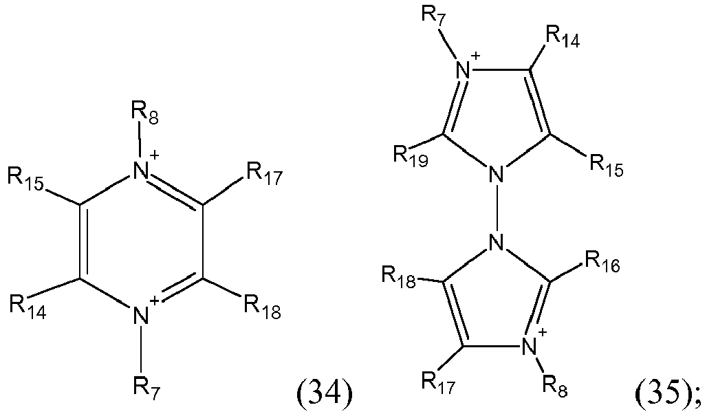
- R7 and R8 are selected from substituents as defined above, and R14, R15, R16, R17, R18, R19, R20 and R21 are independently selected from H, halogen and substituents as defined above for R7, R8, R9 and R10. Preferably, R14, R15, R16, R17, R18, R19, R20 and R21 are selected from H and halogen, most preferably H.
- In the organic cations A, A' and B, hydrogen atoms may be substituted by halogens, such as F, Cl, I, and Br, preferably F or Cl. Such a substitution is expected to reduce the hygroscopic properties of the perovskite layer or layers and may thus provide a useful option for the purpose of the present specification.
- According to a preferred embodiment, A and A' are independently selected from organic cations of formula (20) and/or formula (28).
- According to a preferred embodiment, the metal M is selected from Sn2+ and Pb2+, preferably Pb2+. According to a preferred embodiment, N is Sb3+.
- According to a preferred embodiment, the three or four X are independently selected from Cl-, Br-, and I-.
- The light harvesting compound used in these devices is not restricted to perovskite light absorbers but also comprising of a two dimensional (2D) or three dimensional (3D) or combination of both.
- According to one embodiment, the optoelectronic and/or photovoltaic device of the invention is selected from an organic photovoltaic device, a photovoltaic solid state device, a p-n heterojunction, a metal organohalide perovskite photovoltaic device, a metal organohalide perovskite solar cell, a solid state solar cell, a phototransistor or LED (light-emitting diode).
- According to a further embodiment, the optoelectronic and/or photovoltaic device of the invention is selected from an organic photovoltaic device, a photovoltaic solid state device, a p-n heterojunction, a metal organohalide perovskite photovoltaic device, a metal organohalide perovskite solar cell, or a solid state solar cell.
- The optoelectronic and/or photovoltaic device may be operated in forward bias to serve as a light emitting diode (LED).
- The present invention is described more concretely with reference to the following examples, which, however, are not intended to restrict the scope of the invention.
- Although the present invention has been explained in relation to its preferred embodiment, it is to be understood that many other possible modifications and variations can be made without departing from the scope of the invention as hereinafter claimed.
- FTO glass (NSG-10) was first etched by a chemical method using zinc powder and HCl solution (2 M). To deposit the compact TiO2 layer (c-TiO2), titanium diisopropoxide acetyl acetonate (Sigma-Aldrich) was diluted in ethanol and deposited on substrates at 450 °C by using spray pyrolysis method, followed by 30 min annealing at 450°C. Thereafter, a 150 nm-thick mesoporous TiO2 layer was spin coated on the c-TiO2 (4000 rpm for 15 s with a ramp rate of 2000 rpm/s) using diluted TiO2 paste (
Dyesol 30 NR-D) in ethanol. Then, the substrates were annealed at 450°C for 30 min. After cooling the substrates to 150 °C, they were transferred to the glovebox for perovskite deposition. - The precursor solution was prepared by mixing FAI (1.105 M, Dyesol), PbI2 (1.16 M, TCI), MABr (0.195 M, Dyesol) and PbBr2 (0.195 M, TCI), and CsI (0.068 M, TCI) in DMF:DMSO = 4:1 (volume ratio). The perovskite solution was spin-coated in two-step first at 1000 rpm for 10 s and, then at 4000 rpm for 30 s. During the second step, 200 µL of chlorobenzene (CB) anti-solvent was dropped on top of film 5 s before the end of spinning. Then, the film was annealed at 100 °C for 80 min.
- For passivation of perovskite film, the AD or ADA was either added to the anti-solvent chlorobenzene (anti-solvent (AS) method) or deposited by spin coating as separated layer (spin-coating (SC) method). Thus, in the AS method, perovskite films were passivated during applying anti-solvent on top of the film before annealing, while in the SC technique, after annealing the perovskite film, various solutions of AD and ADA additives with different concentrations were deposited on top of perovskite layer by spin-coating at 4000 rpm for 30 s with a ramp rate of 2000 rpm/s. Afterward, the passivated films were annealed at 120 °C for 10 min. After annealing, spiro-OMeTAD solution in chlorobenzene (70 mM) containing bis(trifluoromethylsulfonyl)imide lithium salt (Li-TFSI, Sigma-Aldrich) solution (520 mg/ml acetonitrile) and (4-tert-butylpyridine-Sigma-Aldrich) with molar ratios of 0.5 and 3.3, respectively, was prepared and spin-coated at 4000 rpm for 20 s with 2000 rpm/s ramp rate. Finally, the device structure was completed by thermal evaporation of 80-nm thick gold as an electrode with an active area of 0.16 cm2.
- 1-aminoadamantane (ADA) and HI or HBr or HCl were mixed with 1:1 molar ratio and ethanol was added into the solution in order to remove water from the solution. Then, the solvent of solution was removed using rotary evaporator at 50 °C in order to get a solid powder as final product. Then the powder was purified using diethyl ether several times.
- Spiro-OMeTAD has been used as a HTL and the spiro-OMeTAD solution was prepared with 70 mM. For doping purpose, first the spiro-OMeTAD (70 mM) and adamantane hydroiodide (ADHI) salts were mixed and dissolved in chlorobenzene with different concentration of ADHI. Then, tBP and bis(trifluoromethylsulfonyl)imide lithium salt (Li-TFSI, Sigma-Aldrich) (520 mg/1 mL acetonitrile) were added into the solution with molar ratios of 3.3 and 0.5, respectively. For ADHI adduct, extra tBP (2 M) was added into the solution to obtain a clear solution. Afterward, the spiro- OMeTAD solutions were spin-coated on top of perovskite film at 4000 rpm for 20 s with ramp rate of 2000 rpm.
- The morphology of perovskite film, and device structure was studied using a ZEISS Merlin high resolution scanning electron microscopy (HRSEM). Quality and crystal structure of perovskite films were characterized by using X-ray diffraction (Bruker D8 X-ray Diffractometer, USA) utilizing a Cu Kα radiation. For optical absorption measurement, a
Varian Carry 500 spectrometer (Varian, USA) was used. To record steady-state photoluminescence spectra, an Edinburgh Instruments FLS920P fluorescence spectrometer, and for photoluminescence lifetime measurement (TRPL), a picosecond pulsed diode laser (EPL-405, excitation wavelength 405 nm, pulse width 49 ps) were employed. In order to analysis of TRPL results, PL decay curves were fitted to the following exponential function I(t)=I0exp(-(t/τ)β), where τ is the decay time and β is a stretch parameter. - The solar cells were measured under AM1.5G sun simulator (a 450 W Xenon lamp (Oriel), with intensity of 100 mWcm-2, equipped with a Schott K113 Tempax sunlight filter (Praezisions Glas & Optik GmbH) to simulate the emission spectra of AM1.5G standard in the region of 350-750 nm. Calibration of the lamp was performed using standard Silicon solar cell. To measure the current density-voltage (J-V) curves, a 2400 series source meter (Keithley, USA) instrument was employed. The voltage range for J- V sweeps was between 0 and 1.2 V, with a step size of 0.005 V and a delay time of 200 ms at each point. External quantum efficiency (EQE) spectra were measured with a commercial apparatus (Arkeo-Ariadne, Cicci Research s.r.l.) based on a 300 Watts Xenon lamp. Ecopia HMS 3000 setup (Microworld) with a magnetic field of 0.54 T in a 4-point configuration was used for Hall effect measurement. For this purpose, the perovskite film was deposited on glass slide using the same method and indium metal was used for electrode at four corners. In addition, the thickness of the perovskite films was controlled by a profiler (Tencor Alpha step 500). A biologic MPG2 potentiostat and a white LED lamp were used to simulate full AM 1.5 Sun-equivalent for stability test. The stability measurement was performed in nitrogen atmosphere under continuous light illumination using a device with active area of masked to 0.16 cm2. The maximum power point (MPP) and J-V curve of devices were recorded every 10 s and every 10 min, respectively.
- According to
Figures 1A-D ,Figures 2A-C andFigure 3A , the passivation of perovskite film with AD or ADA does not significantly affect the morphology of the perovskite film. There is no discernible shift in the UV and PL peaks after incorporation of the additives inside the perovskite film whose band gap is about = 1.61 eV (seeFigure 3B). Figure 3C depicts time resolved photoluminescence (TRPL) traces of perovskite films deposited on glass substrate before and after surface passivation with AD or ADA molecules. The PL lifetimes follow the order ADA > AD > reference illustrating that ADA is most effective in mitigating perovskite surface states acting as charge carrier recombination centers (see Table 1).Table 1. Fitting parameters of the corresponding PL decay curves (τ: time decay, β: a stretch parameter, χ2: fitting range). Sample τ (ns) β χ2 Reference 14.3 0.79 1.01 Passivation with AD 34.6 0.83 1.03 Passivation with ADA 68.4 0.81 1.07 - The device parameters of the solar cells with best performance are summarized in Table 2 (see also
Figures 4A-B ). The reference cell based on triple cation perovskite film gave a Jsc of 22.47 mA/cm2, Voc of 1.083 V, fill factor (FF) of 79.1%, and PCE of 19.32%. In contrast, AD-based device and ADA containing device exhibit significant improvement in Voc. Thus, the PSC based on ADA treatment presents higher PCE up to 20.93% with Jsc of 22.57 mA/cm2, Voc of 1.155 V, and FF of 80.4%, while the AD-based solar cell shows the best performance of 20.47% (Jsc of 22.53 mA/cm2, Voc of 1.142 V, and FF of 79.3%). Notably, all PV parameters are improved by using AD and ADA molecules as additives. Nevertheless, fromFigure 4b and Table 2, the Voc emerges as the metric that profits the most from the ADA surface treatment with an impressive gain of 60 mV over the blank. In addition, the EQE values obtained with the AD and ADA treated samples are slightly higher than those of the reference cell in line with the measured photocurrents (seeFigure 4C ). The projected Jsc values fit well with the measured ones showing that any spectral mismatch between our simulator and the standard AM 1.5 emission is negligibly small. FromFigure 4D , the reference and the AD treated films show practically stable power output over the 60 second tracking time corresponding to 19.12 and 20.35 mW/cm2, respectively. Conversely, the ADA modulated perovskite solar cell shows an additional small rise in the output power until reaching a plateau corresponding to a stabilized PCE of 21.3 %. We infer from these measurements that the ADA surface treatment boosts the power conversion efficiency of our triple cation PSC by a remarkable 11.4 %.Table 2. Figure of merits of perovskite solar cells before and after passivation Sample Voc (V) Jsc (mA/cm2) FF (%) PCE (%) Hysteresis index (%) Reference-forward 1.081 22.43 78.1 19.01 1.65 Reference-backward 1.083 22.47 79.2 19.32 Passivation with AD-forward 1.139 22.48 78.4 20.11 1.73 Passivation with AD-backward 1.142 22.53 79.3 20.47 Passivation with ADA-forward 1.154 22.61 79.1 20.63 1.43 Passivation with ADA-backward 1.155 22.57 80.4 20.93 * Note that the intensity of light was 0.998 sun in this measurement. - In order to ascertain the reproducibility of the effects resulting from surface modification of the perovskite by the adamantanes we produced 30 devices, i.e. 10 for each category and checked the statistical variation of their PV parameters.
Figure 5 shows the PV metrics obtained from the J- V curves of these cells. The results confirm the beneficial effect exerted by the surface treatment by AD and ADA on all the PV parameters the most striking being the enhancement of the Voc. In addition, the results suggest that ADA is more effective in passivating the surface states of perovskite films than AD. We attribute this to stronger surface attachment of the ADA by virtue of its amine group that can anchor to the perovskite surface by replacing an A-cation or by filling an A cation vacancy. The presence of latter defects is undesirable as they act as hole traps immobilizing positively charged carriers at the interface between the perovskite and the spiro-OMeTAD. This enhances carrier recombination and causes hysteresis effects in the J-V curves because the trapped carriers produce a net local electric field that causes ion migration in the perovskite films. - The hysteresis indexes (h) of the passivated devices and reference cell were calculated from the formula h = 100 × (PCEbackward - PCE folward)/PCEbackward. As shown in
Figure 6 , the hysteresis indexes of passivated devices are slightly lower than that of the reference cell.Figure 7 demonstrates the histograms of the photovoltaic metrics of PSCs passivated with AD and ADA by using the antisolvent (AS) technique. From these measurements, the AS treatment produces smaller performance benefits than spin coating the agents onto the perovskite surface (seeFigures 7A-D ). In order to identify the optimal concentration of AD and ADA in the spin coating solvent we varied their content from 0 to 3 mg in 1 mL chlorobenzene and present the photovoltaic parameters of devices treated by these solutions (seeFigures 8A-D andFigures 9A-D ). The data show that the best results are achieved for both additives with a concentration of 1.5 mg/mL. - The contact angle of water on top of the reference sample and the films passivated by AD and ADA was measured (see
Figures 10A-C ) and obtained the values of 35°, 56°, and 68°, respectively. Thus the films after passivation with AD or ADA have lower wettability by water molecules, protecting the perovskite film from water ingression which should enhance their stability. We confirmed that the passivation of perovskite films with AD and ADA molecules does improve the device stability. We first examined the sensitivity of PSCs to humid air by placing unsealed devices for 3 months in an air box with 20 % relative humidity. The result of this stability test is shown inFigure 10D The perovskite whose surface was passivated with AD and ADA maintained 95% and 98% of their initial values, respectively, while the reference cell showed a 16% PCE loss. We subsequently exposed perovskite films on glass with and without surface passivation by the adamantanes to ambient atmosphere for 1 week. The color of reference sample turned from black to yellow, indicating decomposition of perovskite film under formation of PbI2. By contrast, the perovskite film passivated with ADA maintained its black colour while the one modified with AD discolored slightly (seeFigure 11 , XRD patterns of the perovskite films). According toFigure 11 , the intensity of the PbI2 peak located at 12.8° clearly depicts the decomposition of perovskite film under high humidity environment, which is the highest for reference sample. - The operational stability of the devices was examined by exposing them to continuous full-sun illumination under maximum power point tracking in a nitrogen atmosphere at T=30 °C.
Figure 10E illustrates that devices treated with ADA and AD by the SP method retained 96% and 92% of their initial values after 300 h under continuous light illumination, respectively, while the reference sample incurred a 28% performance loss. Our investigations clearly show that the introduction of adamantanes as interfacial layers between the perovskite film and the hole conductor is beneficial for both the performance and operational stability of state of the art perovskite solar cells. -
Figure 12 shows the J- V curves of triple cations perovskite solar cells based on reference and in-situ passivated device with ADHI. As we optimized the concentration of additive for passivation inFigures 5 and7 , we have added the optimum amount of this additive into the HTL solution. As seen, by using this technique, all J-V parameters, especially Voc are improved drastically, resulting in power conversion efficiency (PCE) of 21.85% compared with reference sample (19.65%). Table 3 summarizes the photovoltaic parameters of these devices with different scan directions. As seen, the device based on modified HTL shows high PCE with negligible hysteresis as well. The statistical data for 12 devices with and without HTL doping are shown inFigures 13A-D . The results clearly indicate that the average values of all photovoltaic parameters are improved using our new passivation technique. Interestingly, using this technique the average value of Voc is increased by 100 mV. - In order to study the role of ADHI on operational stability of perovskite solar cell, we have performed stability test under continuous light illumination for 500 h. As shown in
Figure 14 , the modified HTL-based device retains more than 99% of its initial values, while the reference sample shows 25% PCE loss. After checking top-view SEM images of spiro-OMeTAD layers with and without ADHI additive, we discovered that modified spiro-OMeTAD does not have any pinhole and the film is very uniform, while the reference spiro-OMeTAD has many pinholes which can decrease the operational stability of device.Table 3. Figure of merits for reference cell and device with in-situ passivation using ADHI. Sample Voc (V) Jsc (mA/cm2) FF (%) PCE (%) Hysteresis (%) Reference-forward 1.076 22.92 74.5 18.72 4.7 Reference - backward 1.093 23.1 75.6 19.65 ADHI-spiro-forward 1.153 24.25 76.8 21.52 0.44 ADHI-spiro-backward 1.155 24.28 77.2 21.85 - As show in
Figure 13 , we observe a remarkably high Voc which indicates suppressed interfacial recombination upon employing the additive in spiro-OMeTAD. To quantify losses due to non-radiative recombination, we performed an optoelectronic analysis of the devices. We measured the open-circuit voltage at 20 °C without mask under LED light. The data in Fig. 15a shows a maximum value of 1.245, which is a record for lead-iodide based perovskite solar cells. However, the real figure of merit is the so-called voltage deficit as defined as difference between the bandgap/e and the measured Voc. We use the IPCE onset represented in a Tauc plot (Fig. 16) to determine the bandgap. We find a value of 1.61 eV, which is lower compared to e.g. the Rb containing CsMAFA perovskite10, because the composition used here is Cs0.05MA0.15FA0.85Pb(I0.85Br0.15)3. - Hence, the voltage deficit is as low as 365 mV, which is the lowest value reported for any solution processed solar cell (Table 4). Such a low value should come along with high luminescence yields under open circuit conditions. To quantify this yield, we measured electroluminescence (EL), applying a constant current to the solar cell, which is kept in the dark and operated as an LED. The external quantum efficiency of EL reaches 2.5% for a driving current density similar to the short circuit current density (22.5 mA/cm2) (c). This translates into a non-radiative loss as low as 94 meV, clearly surpassing the so far reported record value of 120 meV. Using the reciprocity between absorption and emission, we determine a maximum theoretical Voc of 1.343 V. This value is consistent with the experimental data and the non-radiative losses. Also, the predicted PL peaking at 1.61 matches the measured EL spectrum shown in Fig. 15d. Interestingly, the EL reaches its maximum value after minutes. This is considerably slower to what is reported for non-modified HTL and indicates that applying a forward voltage reduces non-radiative losses, possibly because a redistribution of ions leads to a reduction of surface recombination.
Table 4. Open circuit voltage, electroluminescence, and band gap of device based ADHI modification. Voc max theory 1.343 V EL EQE at 20 mA/cm2 2.5 % Non-rad. loss 94 mV Voc calculated 1.249 V Voc measured 1.245 V Eg 1.61 eV Eg/e - Voc 365 mV EL peak eV 1.61 Eg - EL peak 0.365 -

- To a solution of 4-tert-butyl benzonitrile (10 mmol) was added borane-tetrahydrofuran complex (1M in THF, 40 mL, 40 mmol) under protection of argon. The organic phase was extracted with diethyl ether and dried over sodium sulfide. The organic solvent was removed under reduced pressure, the residue is re-dissolved into 10 mL of tert-butanol and cooled to 0 °C under argon protection. Hydroiodide aqueous solution (53% w/w, 15 mmol) was added dropwise into the solution and the reaction mixture was allowed to stir and 0 °C for 3 h. Upon completion of the reaction, the solvent was removed under reduced pressure. The residue brownish solid was washed with diethyl ether spontaneously until the solid become white and clean. The white solid was dried under vacuum to get the final product as white crystal plate.
-
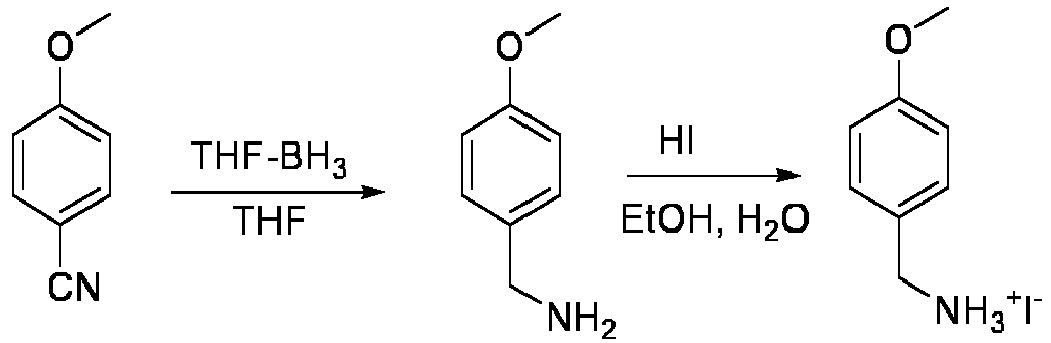
- To a solution of p-hydroxy benzonitrile (8 mmol) and K2CO3 (10 mmol) in ethanol was added methyl iodide dropwise under argon protection. The reaction mixture was allowed to reflux overnight. The solution was filtered and the filtrate solvent was removed under reduced pressure. The residue is re-dissolved into THF and treated with borane-tetrahydrofuran complex (1M in THF, 30 mL, 30 mmol) under protection of argon. The mixed solution was allowed to reflux overnight before quenched with water. The organic phase was extracted with diethyl ether and dried over sodium sulfate. The organic solvent was removed under reduced pressure, the residue is re-dissolved into 10 mL of tert-butanol and cooled to 0 °C under argon protection. Hydroiodide aqueous solution (53% w/w, 10 mmol) was added dropwise into the solution and the reaction mixture was allowed to stir and 0 °C for 3 h. Upon completion of the reaction, the solvent was removed under reduced pressure. The residue brownish solid was washed with diethyl ether spontaneously until the solid become white and clean. The white solid was dried under vacuum to get the final product as white powder.
- 50 mg 4-tert-butylbenzylamino hydroiodide or 4-methoxy benzylamino hydroiodide was dissolved into 1 mL of acetonitrile as stock solution. To 1 mL of spiro-OMeTAD solution (contain 90 mg spiro-OMeTAD, 35.5 µL tert-butyl pyridine, 10.5 mg of LiTFSI) was added 60 µL of the stock solution. The as-prepared mixed spiro-OMeTAD solution was casted onto the perovskite active layer.
Table 5. Figure of merits for reference cell and device with in-situ passivation using 4-TBBHI or 4-MBHI. Photovoltaic Device V OC (V) J SC (mA Cm- 2 )FF PCE (%) Reference 1.121 23.55 0.781 20.6 With 4-TBBHI 1.161 23.53 0.805 22.0 With 4-MBHI 1.125 23.20 0.801 20.9 - In a conclusion, the benzyl based amino iodide additives exhibit significant improvement to the fill factor of the perovskite solar cell devices. In both cases the fill factors could be higher than 80%. Compared to the control devices, the additive modified devices show similar current. Devices with 4-TBBHI, the open-circuit voltage has increased by 40 mV, while with 4-MBHI, the open-circuit voltage is similar to the control devices. Devices based with the alkyl benzyl amines show better passivation effect to the perovskite layer compared to the alkoxy benzyl amines.
Claims (15)
- An optoelectronic and/or photovoltaic device comprising a compound used as crystal defect mitigating agent or passivating agent, said compound being selected from a compound of formula (I)


a compound of formula (III) being a compound of formula (I), of which substituent R is substituted by one compound of formula (II) being linked to said compound of formula (I) through any one of unsubstituted R4, R5, R6, R7 or R8, and wherein the substituent R4, R5, R6, R7 or R8 not being linked are independently selected from any substituent as defined below,
whereinR, R1, R2, R3, R4, R5, R6, R7 and R8 are independently selected from H, -NH2, -NCS, - CN, - NCO, -NH3 +, -NH3 +Y, -R9 -NHR9, -NR9R10, -O-R9, -S-R9, or halogen being selected from F, Cl, Br or I, wherein R9 and R10 are independently selected from C6-C15 aryl, C6-C15 heteroaryl, C3-C15 cycloalkyl group, C3-C15 heterocycloalkyl groups, C1-C15 alkyl group, C1-C15 heteroalkyl group, C2-C15 alkenyl group, C2-C15 alkynyl group, wherein one or more heteroatoms are selected from N, S or O, wherein said alkyl, heteroalkyl, alkenyl and alkynyl group, if they comprise 3 or more carbons, may be linear, branched or cyclic and wherein aryl, heteroaryl, cycloalkyl, heterocycloalkyl, alkyl, heteroalkyl, alkenyl, alkynyl group are unsubstituted or further substituted by halogen being selected from F, Cl, Br or I,Y and W are independently selected from F-, Cl-, Br-, I-, SCN-, BF4 -, PF6 -, ClO4 -, N(SO2CF3)2 -, N(SO2CF2CF3)2 -, CH3SO3 -, CF3SO3 -, CF3COO-, BPh4, C(SO2CF3)3 -, NCS-, CN-, NCO-, andn is an integer from 0, 1 to 5. - The optoelectronic and/or photovoltaic device according to claim 1, wherein the compound used as crystal defect mitigating agent or passivating agent is selected from a compound of formula (I) or a compound of formula (III).
- The optoelectronic and/or photovoltaic device according to any one of the preceding claims, wherein R1, R2, and R3 of the compound of formula (I) or of the compound of formula (III) are H.
- The optoelectronic and/or photovoltaic device according to any one of the preceding claims, wherein R of the compound of formula (I) is selected from H, -NH2, -NH3 +, -NH3 +Y, -R9, -NHR9, -NR9R10, -O-R9, -S-R9, or halogen being selected from F, Cl, Br or I, wherein R9 and R10 are independently selected from C6-C15 aryl, C6-C15 heteroaryl, C3-C15 cycloalkyl group, C3-C15 heterocycloalkyl groups, C1-C15 alkyl group, C1-C15 heteroalkyl group, C2-C15 alkenyl group, C2-C15 alkynyl group, wherein one or more heteroatoms are selected from N, S or O, wherein said alkyl, heteroalkyl, alkenyl and alkynyl group, if they comprise 3 or more carbons, may be linear, branched or cyclic and wherein aryl, heteroaryl, cycloalkyl, heterocycloalkyl, alkyl, heteroalkyl, alkenyl, alkynyl group are unsubstituted or further substituted by halogen being selected from F, Cl, Br or I, and wherein Y is selected from F-, Cl-, Br-, I-, SCN-, BF4 -, PF6 -, ClO4 -, N(SO2CF3)2 -, N(SO2CF2CF3)2 -, CH3SO3 -, CF3SO3 -, CF3COO-, BPh4 -, C(SO2CF3)3 -.
- The optoelectronic and/or photovoltaic device according to any one of the preceding claims, wherein R of the compound of formula (I) is selected from H, -NH2, -NH3 +, -NH3 +Y, wherein Y is selected from F-, Cl-, Br-, I-, SCN-, BF4 -, PF6 -, ClO4 -, N(SO2CF3)2 -, N(SO2CF2CF3)2 -, CH3SO3, CF3SO3 -, CF3COO-, BPh4 -, C(SO2CF3)3.
- The optoelectronic and/or photovoltaic device according to claim 1, wherein the compound used as crystal defect mitigating agent or passivating agent is selected from a compound of formula (II).
- The optoelectronic and/or photovoltaic device according to any one of the preceding claims, wherein R5, R6, R7 and R8 of the compound of formula (II) or, if present, of the compound of formula (III) are H and n is an integer from 1 to 5.
- The optoelectronic and/or photovoltaic device according to any one of the preceding claims, wherein R4 of the compound of formula (II) or, if present, of the compound of formula (III), is selected from H, R9, -NHR9, -NR9R10, -O-R9, -S-R9, or halogen, wherein R9 and R10 are independently selected from C3-C15 cycloalkyl group, C3-C15 heterocycloalkyl groups, C1-C15 alkyl group, C1-C15 heteroalkyl group, C2-C15 alkenyl group, C2-C15 alkynyl group, wherein one or more heteroatoms are selected from N, S or O, wherein said alkyl, heteroalkyl, alkenyl and alkynyl group, if they comprise 3 or more carbons, may be linear, branched or cyclic and wherein cycloalkyl, heterocycloalkyl, alkyl, heteroalkyl, alkenyl, alkynyl group are unsubstituted or further substituted by halogen being selected from F, Cl, Br or I; and n is an integer from 1 to 5.
- The optoelectronic and/or photovoltaic device according to any one of the preceding claims further comprising a light-harvesting layer comprising a metal organohalide perovskite and a hole transport layer comprising a hole transport material, wherein the compound used as crystal defect mitigating agent or passivating agent is infiltrated in the light-harvesting layer and/or coats the top of the light-harvesting layer forming a layer being a passivation layer and/or is included into the hole transport layer, and wherein the hole transport layer is in electric contact with the light-harvesting layer and/or the passivation layer.
- The optoelectronic and/or photovoltaic device according to claim 9 further comprising a conducting support layer, n-type semiconductor, an electron transport layer and a back contact, wherein the n-type semiconductor is in electric contact with the conducting support layer and the electron transport layer is in electric contact with the n-type semiconductor; and the back contact is in electric contact with the hole transport layer.
- The optoelectronic and/or photovoltaic device according to any one of claims 9-10, wherein the metal organohalide perovskite is selected from a perovskite structure according to any one of formulae (I), (Ia), (Ib), (Ic), (Id), (Ie), (If) and/or (Ig) below:
AA'MX4 (I) AMX3 (Ia) AA'N2/3X4 (Ib) AN2/3X3 (Ic) BN2/3X4 (Id) BMX4 (Ie) (Al)mAA'MX3 (If) (Al)mAMX3 (Ig) - A and A' are organic, monovalent cations being independently selected from primary, secondary, tertiary or quaternary organic ammonium compounds, including N-containing heterorings and ring systems, A and A' having independently from 1 to 60 carbons and 1 to 20 heteroatoms;- A1 is an inorganic cation selected from Cs+, Rb+, K+ and m is an integer from 1 to 3, each A1 if m >1 being different;- B is an organic, bivalent cation selected from primary, secondary, tertiary or quaternary organic ammonium compounds having from 1 to 60 carbons and 2-20 heteroatoms and having two positively charged nitrogen atoms;- M is selected from Cu2+, Ni2+, Co2+, Fe,2+ Mn2+, Cr2+, Pd2+, Cd2+, Ge2+, Sn2+, Pb2+, Eu2+, Yb2+, [SniPb(1-i)]+, [SnjGe(1-j)]+, and [PbkGe(1-k)]+, i, j and k being a number between 0.0 and 1.0;- N is selected from the group of Bi3+ and Sb3+; and,- X are independently selected from Cl-, Br-, I-, NCS-, CN-, NCO-, from [I(3-o)Clo]-, [I(3-p)Brp]-, [Br(3-u)Clu]-, o, p and u being a number between 0.0 and 3.0, and from a combination of two anions selected from Cl-, Br-, I-. - The optoelectronic and/or photovoltaic device according to any one of claims 9-11, wherein the hole transport material is selected from semiconductor particles comprising NiO, CuO, CuSCN, CuI, CuGaO2, CuCrO2 or CuAlO2 or any combination thereof or from triphenylamine, carbazole, N,N,(diphenyl)-N',N'di-(alkylphenyl)-4,4'-biphenyldiamine, (pTPDs), diphenylhydrazone, poly [N,N'-bis(4-butylphenyl)-N,N'-bis(phenyl)benzidine] (polyTPD), polyTPD substituted by electron donor groups and/or acceptor groups, poly(9,9-dioctylfluorene-alt-N-(4-butylphenyl)-diphenylamine (TFB), 2,2',7,7'-tetrakis-N,N-di-p-methoxyphenylamine-9,9'-spirobifluorene) (spiro-OMeTAD), N,N,N',N'-tetraphenylbenzidine (TPD), PTAA (Poly[bis(4-phenyl)(2,4,6-trimethylphenyl)amine]).
- The optoelectronic and/or photovoltaic device according to any one of claims 10-12, wherein the electron transport layer comprises an amorphous metal oxide layer.
- The optoelectronic and/or photovoltaic device according to any one of the preceding claims is selected from an organic photovoltaic device, a photovoltaic solid state device, a p-n heterojunction, a metal organohalide perovskite photovoltaic device, a metal organohalide perovskite solar cell, a solid state solar cell, a phototransistor or LED (light-emitting diode).
- The optoelectronic and/or photovoltaic device according to any one of the preceding claims is selected from an organic photovoltaic device, a photovoltaic solid state device, a p-n heterojunction, a metal organohalide perovskite photovoltaic device, a metal organohalide perovskite solar cell, or a solid state solar cell.
Priority Applications (3)
| Application Number | Priority Date | Filing Date | Title |
|---|---|---|---|
| EP18153309.2A EP3518301A1 (en) | 2018-01-24 | 2018-01-24 | Crystal defects mitigating agents for high power conversion efficiency and stability of perovskite photovoltaic devices |
| US16/964,793 US20210054288A1 (en) | 2018-01-24 | 2019-01-21 | Crystal defects mitigating agents for high power conversion efficiency and stability of perovskyte photovoltaic devices |
| PCT/IB2019/050485 WO2019145841A1 (en) | 2018-01-24 | 2019-01-21 | Crystal defects mitigating agents for high power conversion efficiency and stability of perovskite photovoltaic devices |
Applications Claiming Priority (1)
| Application Number | Priority Date | Filing Date | Title |
|---|---|---|---|
| EP18153309.2A EP3518301A1 (en) | 2018-01-24 | 2018-01-24 | Crystal defects mitigating agents for high power conversion efficiency and stability of perovskite photovoltaic devices |
Publications (1)
| Publication Number | Publication Date |
|---|---|
| EP3518301A1 true EP3518301A1 (en) | 2019-07-31 |
Family
ID=61054180
Family Applications (1)
| Application Number | Title | Priority Date | Filing Date |
|---|---|---|---|
| EP18153309.2A Withdrawn EP3518301A1 (en) | 2018-01-24 | 2018-01-24 | Crystal defects mitigating agents for high power conversion efficiency and stability of perovskite photovoltaic devices |
Country Status (3)
| Country | Link |
|---|---|
| US (1) | US20210054288A1 (en) |
| EP (1) | EP3518301A1 (en) |
| WO (1) | WO2019145841A1 (en) |
Cited By (3)
| Publication number | Priority date | Publication date | Assignee | Title |
|---|---|---|---|---|
| CN110862702A (en) * | 2019-11-05 | 2020-03-06 | 南京邮电大学 | Lead-free tin-based halide perovskite thin film, preparation method and application thereof |
| CN110993798A (en) * | 2019-12-20 | 2020-04-10 | 北京大学 | Perovskite type solar cell based on cooperative post-treatment of multiple ammonium salts and preparation method thereof |
| CN112687807A (en) * | 2020-12-28 | 2021-04-20 | 河北工业大学 | 2D/3D hybrid perovskite solar cell prepared based on two-step method |
Families Citing this family (6)
| Publication number | Priority date | Publication date | Assignee | Title |
|---|---|---|---|---|
| US11282700B2 (en) * | 2019-04-17 | 2022-03-22 | University Of Kentucky Research Foundation | Method for manufacturing perovskite-based devices in ambient air |
| WO2022066707A1 (en) | 2020-09-22 | 2022-03-31 | Caelux Corporation | Methods and devices for integrated tandem solar module fabrication |
| CN117999864A (en) * | 2021-12-31 | 2024-05-07 | 宁德时代新能源科技股份有限公司 | Perovskite solar cell and method of manufacture |
| CN115036427B (en) * | 2022-06-10 | 2023-04-07 | 重庆大学 | Buried interface defect passivation and stress release based on adamantane derivative and perovskite solar cell preparation method thereof |
| CN121099827A (en) * | 2024-06-07 | 2025-12-09 | 宁德时代新能源科技股份有限公司 | Solar cell, passivation material, photovoltaic system, electric equipment and power generation equipment |
| DE102024210214A1 (en) | 2024-10-22 | 2026-04-23 | Karlsruher Institut für Technologie, Körperschaft des öffentlichen Rechts | Solar cell containing an adamantane and/or a diadamantane-based passivation layer |
Citations (3)
| Publication number | Priority date | Publication date | Assignee | Title |
|---|---|---|---|---|
| US20090159131A1 (en) * | 2007-12-19 | 2009-06-25 | Honeywell International Inc. | Quantum dot solar cell with rigid bridge molecule |
| JP2015216359A (en) * | 2014-04-25 | 2015-12-03 | 富士フイルム株式会社 | Photoelectric conversion device, solar battery using the same, and method for manufacturing photoelectric conversion device |
| EP3136461A1 (en) * | 2014-04-25 | 2017-03-01 | Fujifilm Corporation | Photoelectric conversion element, solar cell in which same is used, and method for manufacturing photoelectric conversion element |
Family Cites Families (2)
| Publication number | Priority date | Publication date | Assignee | Title |
|---|---|---|---|---|
| WO2016060181A1 (en) * | 2014-10-14 | 2016-04-21 | 積水化学工業株式会社 | Solar cell |
| WO2018011597A1 (en) * | 2016-07-15 | 2018-01-18 | Cristal Pigment Uk Limited | Solar cell materials for increased efficiency |
-
2018
- 2018-01-24 EP EP18153309.2A patent/EP3518301A1/en not_active Withdrawn
-
2019
- 2019-01-21 US US16/964,793 patent/US20210054288A1/en not_active Abandoned
- 2019-01-21 WO PCT/IB2019/050485 patent/WO2019145841A1/en not_active Ceased
Patent Citations (3)
| Publication number | Priority date | Publication date | Assignee | Title |
|---|---|---|---|---|
| US20090159131A1 (en) * | 2007-12-19 | 2009-06-25 | Honeywell International Inc. | Quantum dot solar cell with rigid bridge molecule |
| JP2015216359A (en) * | 2014-04-25 | 2015-12-03 | 富士フイルム株式会社 | Photoelectric conversion device, solar battery using the same, and method for manufacturing photoelectric conversion device |
| EP3136461A1 (en) * | 2014-04-25 | 2017-03-01 | Fujifilm Corporation | Photoelectric conversion element, solar cell in which same is used, and method for manufacturing photoelectric conversion element |
Non-Patent Citations (1)
| Title |
|---|
| C. SAE-KUNG ET AL: "The effect of hydrophobic absorbent for reducing charge recombination to improve dye-sensitized solar cell performance", PROCEEDINGS OF SPIE, vol. 6656, 13 September 2007 (2007-09-13), 1000 20th St. Bellingham WA 98225-6705 USA, pages 665617, XP055491715, ISSN: 0277-786X, ISBN: 978-1-5106-1533-5, DOI: 10.1117/12.733551 * |
Cited By (5)
| Publication number | Priority date | Publication date | Assignee | Title |
|---|---|---|---|---|
| CN110862702A (en) * | 2019-11-05 | 2020-03-06 | 南京邮电大学 | Lead-free tin-based halide perovskite thin film, preparation method and application thereof |
| CN110862702B (en) * | 2019-11-05 | 2021-07-30 | 南京邮电大学 | Lead-free tin-based halide perovskite thin film, preparation method and application thereof |
| CN110993798A (en) * | 2019-12-20 | 2020-04-10 | 北京大学 | Perovskite type solar cell based on cooperative post-treatment of multiple ammonium salts and preparation method thereof |
| CN110993798B (en) * | 2019-12-20 | 2021-11-19 | 北京大学 | Perovskite type solar cell based on synergistic post-treatment of multiple ammonium salts and preparation thereof |
| CN112687807A (en) * | 2020-12-28 | 2021-04-20 | 河北工业大学 | 2D/3D hybrid perovskite solar cell prepared based on two-step method |
Also Published As
| Publication number | Publication date |
|---|---|
| WO2019145841A1 (en) | 2019-08-01 |
| US20210054288A1 (en) | 2021-02-25 |
Similar Documents
| Publication | Publication Date | Title |
|---|---|---|
| JP7681336B2 (en) | Optoelectronic Devices | |
| Wu et al. | Interface modification to achieve high-efficiency and stable perovskite solar cells | |
| US20210054288A1 (en) | Crystal defects mitigating agents for high power conversion efficiency and stability of perovskyte photovoltaic devices | |
| JP7129066B2 (en) | Mixed cation perovskite solid-state solar cells and their fabrication | |
| JP7166613B2 (en) | High-efficiency large-area perovskite solar cell and its manufacturing method | |
| US11594694B2 (en) | Inorganic hole conductor based perovskite photoelectric conversion device with high operational stability at long term | |
| EP3381070B1 (en) | Mixed cation perovskite | |
| EP3044817B1 (en) | Inverted solar cell and process for producing the same | |
| EP3499597A1 (en) | Electron specific oxide double layer contacts for highly efficient and uv stable perovskite device | |
| EP2966703A1 (en) | Template enhanced organic inorganic perovskite heterojunction photovoltaic device | |
| EP3667751A1 (en) | Passivation of metal halide perovskites | |
| US20220310929A1 (en) | Optoelectronic device | |
| US20160086739A1 (en) | High performance perovskite-sensitized mesoscopic solar cells | |
| KR20210095916A (en) | Long-term stable optoelectronic devices | |
| EP3223323A1 (en) | High efficiency large area perovskite solar cells and process for producing the same | |
| EP2804232A1 (en) | High performance perovskite-sensitized mesoscopic solar cells |
Legal Events
| Date | Code | Title | Description |
|---|---|---|---|
| PUAI | Public reference made under article 153(3) epc to a published international application that has entered the european phase |
Free format text: ORIGINAL CODE: 0009012 |
|
| STAA | Information on the status of an ep patent application or granted ep patent |
Free format text: STATUS: THE APPLICATION HAS BEEN PUBLISHED |
|
| AK | Designated contracting states |
Kind code of ref document: A1 Designated state(s): AL AT BE BG CH CY CZ DE DK EE ES FI FR GB GR HR HU IE IS IT LI LT LU LV MC MK MT NL NO PL PT RO RS SE SI SK SM TR |
|
| AX | Request for extension of the european patent |
Extension state: BA ME |
|
| STAA | Information on the status of an ep patent application or granted ep patent |
Free format text: STATUS: THE APPLICATION IS DEEMED TO BE WITHDRAWN |
|
| 18D | Application deemed to be withdrawn |
Effective date: 20200201 |