EP3517942A1 - Biosensor - Google Patents
Biosensor Download PDFInfo
- Publication number
- EP3517942A1 EP3517942A1 EP17873094.1A EP17873094A EP3517942A1 EP 3517942 A1 EP3517942 A1 EP 3517942A1 EP 17873094 A EP17873094 A EP 17873094A EP 3517942 A1 EP3517942 A1 EP 3517942A1
- Authority
- EP
- European Patent Office
- Prior art keywords
- electrode
- electrode layer
- layer
- type channel
- drain
- Prior art date
- Legal status (The legal status is an assumption and is not a legal conclusion. Google has not performed a legal analysis and makes no representation as to the accuracy of the status listed.)
- Granted
Links
Images

Classifications
-
- G—PHYSICS
- G01—MEASURING; TESTING
- G01N—INVESTIGATING OR ANALYSING MATERIALS BY DETERMINING THEIR CHEMICAL OR PHYSICAL PROPERTIES
- G01N27/00—Investigating or analysing materials by the use of electric, electrochemical, or magnetic means
- G01N27/26—Investigating or analysing materials by the use of electric, electrochemical, or magnetic means by investigating electrochemical variables; by using electrolysis or electrophoresis
- G01N27/28—Electrolytic cell components
- G01N27/30—Electrodes, e.g. test electrodes; Half-cells
- G01N27/327—Biochemical electrodes, e.g. electrical or mechanical details for in vitro measurements
- G01N27/3275—Sensing specific biomolecules, e.g. nucleic acid strands, based on an electrode surface reaction
-
- G—PHYSICS
- G01—MEASURING; TESTING
- G01N—INVESTIGATING OR ANALYSING MATERIALS BY DETERMINING THEIR CHEMICAL OR PHYSICAL PROPERTIES
- G01N27/00—Investigating or analysing materials by the use of electric, electrochemical, or magnetic means
- G01N27/26—Investigating or analysing materials by the use of electric, electrochemical, or magnetic means by investigating electrochemical variables; by using electrolysis or electrophoresis
- G01N27/28—Electrolytic cell components
- G01N27/30—Electrodes, e.g. test electrodes; Half-cells
- G01N27/327—Biochemical electrodes, e.g. electrical or mechanical details for in vitro measurements
-
- H—ELECTRICITY
- H10—SEMICONDUCTOR DEVICES; ELECTRIC SOLID-STATE DEVICES NOT OTHERWISE PROVIDED FOR
- H10D—INORGANIC ELECTRIC SEMICONDUCTOR DEVICES
- H10D30/00—Field-effect transistors [FET]
- H10D30/60—Insulated-gate field-effect transistors [IGFET]
-
- H—ELECTRICITY
- H10—SEMICONDUCTOR DEVICES; ELECTRIC SOLID-STATE DEVICES NOT OTHERWISE PROVIDED FOR
- H10D—INORGANIC ELECTRIC SEMICONDUCTOR DEVICES
- H10D30/00—Field-effect transistors [FET]
- H10D30/60—Insulated-gate field-effect transistors [IGFET]
- H10D30/791—Arrangements for exerting mechanical stress on the crystal lattice of the channel regions
- H10D30/797—Arrangements for exerting mechanical stress on the crystal lattice of the channel regions being in source or drain regions, e.g. SiGe source or drain
-
- H—ELECTRICITY
- H10—SEMICONDUCTOR DEVICES; ELECTRIC SOLID-STATE DEVICES NOT OTHERWISE PROVIDED FOR
- H10D—INORGANIC ELECTRIC SEMICONDUCTOR DEVICES
- H10D30/00—Field-effect transistors [FET]
- H10D30/60—Insulated-gate field-effect transistors [IGFET]
- H10D30/791—Arrangements for exerting mechanical stress on the crystal lattice of the channel regions
- H10D30/798—Arrangements for exerting mechanical stress on the crystal lattice of the channel regions being provided in or under the channel regions
-
- G—PHYSICS
- G01—MEASURING; TESTING
- G01N—INVESTIGATING OR ANALYSING MATERIALS BY DETERMINING THEIR CHEMICAL OR PHYSICAL PROPERTIES
- G01N27/00—Investigating or analysing materials by the use of electric, electrochemical, or magnetic means
- G01N27/26—Investigating or analysing materials by the use of electric, electrochemical, or magnetic means by investigating electrochemical variables; by using electrolysis or electrophoresis
- G01N27/403—Cells and electrode assemblies
- G01N27/414—Ion-sensitive or chemical field-effect transistors, i.e. ISFETS or CHEMFETS
- G01N27/4145—Ion-sensitive or chemical field-effect transistors, i.e. ISFETS or CHEMFETS specially adapted for biomolecules, e.g. gate electrode with immobilised receptors
-
- G—PHYSICS
- G01—MEASURING; TESTING
- G01N—INVESTIGATING OR ANALYSING MATERIALS BY DETERMINING THEIR CHEMICAL OR PHYSICAL PROPERTIES
- G01N27/00—Investigating or analysing materials by the use of electric, electrochemical, or magnetic means
- G01N27/26—Investigating or analysing materials by the use of electric, electrochemical, or magnetic means by investigating electrochemical variables; by using electrolysis or electrophoresis
- G01N27/403—Cells and electrode assemblies
- G01N27/414—Ion-sensitive or chemical field-effect transistors, i.e. ISFETS or CHEMFETS
- G01N27/4148—Integrated circuits therefor, e.g. fabricated by CMOS processing
Definitions
- the present invention relates to a biosensor.
- the biosensor related to one aspect of the present invention comprises a sensing part, and a cover member mounted on the sensing part and forming a fluid channel in a space therebetween.
- the sensing part comprises a substrate, a gate electrode provided on the substrate, an insulating layer provided on the gate electrode, an n-type channel formed on the insulating layer, and a first electrode layer that forms a source electrode and a drain electrode, respectively, which are located apart from each other, on the n-type channel layer.
- the sensing part comprises a second electrode layer provided so as to surround the first electrode layer, and a third electrode layer located on the substrate and formed of the same material as the first electrode layer.
- the sensing part comprises a fourth electrode layer provided so as to surround the third electrode layer, formed of the same material as the second electrode layer and providing a reference electrode.
- the cover member has an inner periphery surrounding the n-type channel exposed between the source electrode and the drain electrode in the first electrode layer and some areas of the reference electrode together.
- the cover member forms a fluid channel provided so that a fluid can enter into a space between the n-type channel and the inner periphery and a space between the reference electrode and the inner periphery.
- the biosensor related to at least one example of the present invention can easily manufacture a thin film type biosensor element comprising a reference electrode layer by a printing technique, is capable of mass production, and can measure a large amount of detection factors individually/continuously.
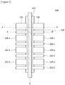
- Figure 1 is a conceptual diagram of a biosensor related to one example of the present invention
- Figure 2 is a cross-sectional view of a state cut along the line A-A' in Figure 1
- Figure 3 is a cross-sectional view of a state cut along the line B-B' in Figure 1 .
- the biosensor (100) comprises a sensing part and a cover member (190) mounted on the sensing part and forming a fluid channel (C) in a space therebetween.
- the sensing part comprises a substrate (110), a gate electrode (140), an insulating layer (150), an n-type channel (160), a first electrode layer (170), a second electrode layer (180), a third electrode layer (200), and a fourth electrode layer (210).
- the first electrode layer (170) forms a source electrode (120) and a drain electrode (130) on the n-type channel (160), respectively.
- the second electrode layer (180) is provided to surround the first electrode layer (170). Specifically, the second electrode layer (180) is provided to surround the source electrode (120) and the drain electrode (130), which are the first electrode layer (170), respectively.
- the biosensor (100) comprises a third electrode layer (200) located on the substrate (110) and formed of the same material as the first electrode layer (170), and a fourth electrode layer (180) provided so as to surround the third electrode layer (200), formed of the same material as the second electrode layer (180) and providing a reference electrode.
- the biosensor (100) comprises a substrate (110), a gate electrode (140) provided on the substrate (110), an insulating layer (150) provided on the gate electrode (140), and an n-type channel (160) provided on the insulating layer (150).
- the substrate (110) a glass substrate or a plastic substrate may be used, and it is not particularly limited as long as it is applied to the biosensor (100).
- the gate electrode (140) may be formed of a metal, which may be selected from the group consisting of, for example, chromium (Cr), molybdenum (Mo), aluminum (Al), titanium/silver (Ti/Au), gold (Ag), copper (Cu) and platinum (Pt).
- Cr chromium
- Mo molybdenum
- Al aluminum
- Ti/Au titanium/silver
- Au gold
- Cu copper
- platinum platinum
- the insulating layer (150) may be formed of SiO2, Al2O3, TiO2, ZrO2, HfO2, SiNx, or the like.
- the usable n-type channel (160) in the present invention may be made of any one n-type material selected from the group consisting of IGZO, ZnO, ZTO, IZO, IHZO, AIN, InN, GaN and InGaN.
- the n-type channel (160) made of IGZO is preferable because it has excellent optical transparency, amorphous structure, high electron mobility, and further, the IGZO channel can function as an active matrix backplane, so that it has an advantage that a separate integration process can be omitted.
- the biosensor (100) comprises a source electrode (120) and a drain electrode (130), provided apart at a predetermined interval, on the n-type channel (160). Furthermore, the biosensor (100) comprises a second electrode layer (180) provided to surround the source electrode (120) and the drain electrode (130), which are the first electrode layer (170), respectively, and a fourth electrode layer (210) located apart from the source electrode (120) and the drain electrode (130), formed of the same material as the second electrode layer (180) and providing a reference electrode.
- the source electrode (120) and the drain electrode (130), which are the first electrode layer (170), may be formed of a metal, which may be selected from the group consisting of, for example, chromium (Cr), titanium/silver (Ti/Au), molybdenum (Mo), aluminum (Al), silver (Ag), copper (Cu), platinum (Pt) and tungsten (W).
- a metal which may be selected from the group consisting of, for example, chromium (Cr), titanium/silver (Ti/Au), molybdenum (Mo), aluminum (Al), silver (Ag), copper (Cu), platinum (Pt) and tungsten (W).
- the biosensor (100) comprises a cover member (190) having an inner periphery (191) surrounding the n-type channel layer (160) exposed between the source electrode (120) and the drain electrode (130), and some areas of the reference electrode together.
- the cover member (190) forms a fluid channel (C) provided so that a fluid (for example, a sample solution) can enter into a space between the exposed n-type channel (160) and the inner periphery (191) and a space between the reference electrode, which is the fourth electrode layer (200), and the inner periphery (191).
- the cover member (190) may be formed of silicone or the like, and for example, may be formed of PDMS.
- a collecting part (R) may also be provided on the n-type channel (160) exposed to the inside of the fluid channel (C).
- the source electrode (120) and the drain electrode (130), which are the first electrode layer (170), are located outside the fluid channel (C). That is, the source electrode (120) and the drain electrode (130) are provided so as not to be in direct contact with a sample solution. Also, the reference electrode, which is the fourth electrode layer (200), is exposed to the inside of the fluid channel (C) so as to be in contact with the sample solution.
- the second electrode layer (180) and the first electrode layer (170) may be formed of different materials (for example, different metal materials).
- the second electrode layer (180) and the fourth electrode layer (210) may be formed of, for example, a noble metal, and specifically, may be formed of one or more selected from the group consisting of gold (Au), palladium (Pd), platinum (Pt), silver (Au), and ruthenium (Ru).
- the gate electrode (140) and the insulating layer (150) may be sequentially located between the substrate (110) and the third electrode layer (200).
- the n-type channel (160) may be sequentially located between the insulating layer (150) and the third electrode layer (200).
- the fourth electrode layer (210) is formed on the n-type channel (160) or on the third electrode layer (200). That is, the fourth electrode layer (210) providing a reference electrode may be formed such that it is disposed on the substrate (110), and thus some areas are located in the fluid channel (C).
- the third electrode layer (200) may be formed even on the bottom of the fourth electrode layer (210). Also, the first electrode layer (170) and the third electrode layer (200) may be formed and then the second electrode layer (180) and the fourth electrode layer (210) may be formed with the same mask. That is, by using a printing technique, the manufacturing process can be simplified.
- n-type channel (160) When a constant voltage is applied between the source electrode (120) and the gate electrode (140) in a TFT, a conduction channel is formed in the n-type channel (160), whereby electrons can move between the source electrode (120) and the drain electrode (130). Then, when target biomolecules of the sample solution are adsorbed and the potential energy of the surface is changed, the amount of current flowing through the n-type conduction channel (160) is changed, so that the presence or concentration of the target biomolecules is calculated from such a change of current.
- the biosensor (100) may be provided so that a large amount of detection factors can be individually/continuously measured in one solution.
- the biosensor (100) comprises a substrate (110), a gate electrode (140) elongated along a first direction on the substrate (110), an insulating layer (150) provided on the gate electrode (140), and an n-type channel (160) provided on the insulating layer (150).
- the biosensor (100) comprises a first electrode layer (170) forming a first source electrode (120-1) and a first drain electrode (130-1), provided apart at a predetermined interval along a second direction different from the first direction on the n-type channel (160), and a second source electrode (120-2) and a second drain electrode (130-2), located apart from the first source electrode (120-1) and the first drain electrode (130-1) along the first direction and provided apart at a predetermined interval along the second direction on the n-type channel (160), respectively.
- the first direction may indicate a direction in which a fluid flows in the fluid channel
- the second direction may indicate a connection line direction of the source electrode and the drain electrode.
- the first direction and the second direction may be directions substantially orthogonal to each other.
- the biosensor (100) comprises a second electrode layer (180) provided so as to surround the source electrode (120) and the drain electrode (130), which are the first electrode layer (170), respectively.
- the biosensor (100) comprises a third electrode layer (200) located on the substrate (110) and formed of the same material as the first electrode layer (170). Also, the biosensor (100) comprises a fourth electrode layer (210) provided on the third electrode layer (200), where the fourth electrode layer (210) provides a first reference electrode and a second reference electrode, respectively.
- the first reference electrode (210-1) constitutes a first sensing part with the first source/drain electrodes (120-1, 130-1)
- the second reference electrode (210-2) constitutes a second sensing part with the second source/drain electrodes (120-2, 130-2).
- the fourth electrode layer (210) comprises the first reference electrode (210-1) located apart from the first source electrode (120-1) and the first drain electrode (130-1) along the first direction and formed of the same material as the second electrode layer (180) so as to surround the third electrode layer (200), and the second reference electrode located apart from the second source electrode (120-2) and the second drain electrode (130-2) along the first direction and formed of the same material as the second electrode layer (180) so as to surround the third electrode layer (200).
- one sensor (first sensing part) function is performed by setting the first reference electrode (210-1) to the reference potential of a reaction and measuring the current between the first source electrode (120-1) and the first drain electrode (130-1).
- another sensor (second sensing part) function is performed by setting the second reference electrode (210-2) to the reference potential of a reaction and measuring the current between the second source electrode (120-2) and the second drain electrode (130-2).
- a plurality of sensing parts can be formed in one fluid channel (C).
- the biosensor (100) comprises a cover member (190), where the cover member (190) has an inner periphery (191) surrounding the n-type channel exposed between the first source electrode (120-1) and the first drain electrode (130-1), the n-type channel exposed between the second source electrode (120-2) and the second drain electrode (130-2) and some areas of each of the first and second reference electrodes together. Then, the cover member (190) forms a fluid channel (C) provided such that a fluid can enter into a space between the exposed n-type channels and the inner periphery and a space between the first and second reference electrodes and the inner periphery.
- a fluid channel C
- the fluid channel (C) is elongated along the first direction.
- the first source and drain electrodes (120-1, 130-1), the first reference electrode (210-1), the second source and drain electrodes (120-2, 130-2), and the second reference electrode (210-2) are sequentially positioned.
- the first source and first drain electrodes (120-1, 130-1) and the second source and drain electrodes (120-2, 130-2) are the same as the source and drain electrodes (120, 130) as described above, respectively, but only the positions formed along the first direction on the gate electrode are different. Also, the first and second reference electrodes (210-1, 210-2) are the same as the reference electrode as described above.
- the first sensing part and the second sensing part are provided to be independently drivable. That is, the biosensor (100) may comprise a plurality of sensing parts, and the sensing parts may be each provided to be independently drivable. Also, when the sample solution flows into the fluid channel (C), the biosensor (100) has a structure in which a number of sensing parts are arranged along the fluid channel (C).
- each of the reference electrodes (210-1, 210-2) may be formed such that it is disposed on the substrate (110), and thus some areas are located in the fluid channel (C).
- the third electrode layer (200) may be formed even on the bottom of the relevant reference electrodes (200-1, 200-2).
- a substrate (110), a gate electrode (140), an insulating layer (150), an n-type channel (160), a third electrode layer (200) and a fourth electrode layer (210) may be sequentially provided.
- the second electrode layer (180) and the fourth electrode layer (210) may be formed simultaneously with the same mask used to form the first electrode layer (170) and the third electrode layer (200), and thus the manufacturing process can be simplified by using the printing technique.
- the biosensor (100) related to one example of the present invention may comprise N (N>1) sensing parts, and for example, may comprise a third sensing part containing a third source electrode (120-3) and a third drain electrode (130-3), and a third reference electrode (210-3).
- the biosensor related to at least one example of the present invention can easily manufacture a thin film type biosensor element comprising a reference electrode layer by a printing technique, is capable of mass production, and can measure a large amount of detection factors individually/continuously.
Landscapes
- Life Sciences & Earth Sciences (AREA)
- Health & Medical Sciences (AREA)
- Chemical & Material Sciences (AREA)
- Physics & Mathematics (AREA)
- Molecular Biology (AREA)
- General Physics & Mathematics (AREA)
- Pathology (AREA)
- Analytical Chemistry (AREA)
- Biochemistry (AREA)
- General Health & Medical Sciences (AREA)
- Chemical Kinetics & Catalysis (AREA)
- Immunology (AREA)
- Electrochemistry (AREA)
- Spectroscopy & Molecular Physics (AREA)
- Engineering & Computer Science (AREA)
- Microelectronics & Electronic Packaging (AREA)
- Investigating Or Analyzing Materials By The Use Of Electric Means (AREA)
- Thin Film Transistor (AREA)
- Electrodes Of Semiconductors (AREA)
- Measuring Or Testing Involving Enzymes Or Micro-Organisms (AREA)
- Apparatus Associated With Microorganisms And Enzymes (AREA)
Abstract
Description
- The present invention relates to a biosensor.
- The present application claims the benefit of priority based on Korean Patent Application No.
10-2016-0156375 filed on November 23, 2016 - Among biosensors that detect biomaterials, researches on transistor-based biosensors have been actively conducted.
- On the other hand, conventional biosensors for adsorbing/measuring liquid molecules using a transistor have been made by pouring a liquid from above and have been used by immersing Ag/AgCl, which is a reference electrode, on this solution, but they are not only difficult to quantitatively measure a precise solution, but also have a problem that it is difficult to form a three-dimensional reference electrode on a mass production type printed-electrode substrate.
- It is one problem to be resolved by the present invention to provide a biosensor capable of easily manufacturing a thin film type biosensor element comprising a reference electrode layer by a printing technique and capable of mass production.
- Also, it is another problem to be resolved by the present invention to provide a biosensor capable of individually/continuously measuring a large amount of detection factors in one solution.
- To solve the above-described problems, the biosensor related to one aspect of the present invention comprises a sensing part, and a cover member mounted on the sensing part and forming a fluid channel in a space therebetween.
- The sensing part comprises a substrate, a gate electrode provided on the substrate, an insulating layer provided on the gate electrode, an n-type channel formed on the insulating layer, and a first electrode layer that forms a source electrode and a drain electrode, respectively, which are located apart from each other, on the n-type channel layer.
- Also, the sensing part comprises a second electrode layer provided so as to surround the first electrode layer, and a third electrode layer located on the substrate and formed of the same material as the first electrode layer.
- Furthermore, the sensing part comprises a fourth electrode layer provided so as to surround the third electrode layer, formed of the same material as the second electrode layer and providing a reference electrode.
- In addition, the cover member has an inner periphery surrounding the n-type channel exposed between the source electrode and the drain electrode in the first electrode layer and some areas of the reference electrode together.
- Besides, the cover member forms a fluid channel provided so that a fluid can enter into a space between the n-type channel and the inner periphery and a space between the reference electrode and the inner periphery.
- As described above, according to the biosensor related to at least one example of the present invention, it can easily manufacture a thin film type biosensor element comprising a reference electrode layer by a printing technique, is capable of mass production, and can measure a large amount of detection factors individually/continuously.
-
-
Figure 1 is a conceptual diagram of a biosensor related to one example of the present invention. -
Figure 2 is a cross-sectional view of a state cut along the line A-A' inFigure 1 . -
Figure 3 is a cross-sectional view of a state cut along the line B-B' inFigure 1 . - Hereinafter, a biosensor according to one example of the present invention will be described in detail with reference to the accompanying drawings.
- In addition, the same or similar reference numerals are given to the same or corresponding components regardless of reference numerals, of which redundant explanations will be omitted, and for convenience of explanation, the size and shape of each constituent member as shown may be exaggerated or reduced.
-
Figure 1 is a conceptual diagram of a biosensor related to one example of the present invention,Figure 2 is a cross-sectional view of a state cut along the line A-A' inFigure 1 , andFigure 3 is a cross-sectional view of a state cut along the line B-B' inFigure 1 . - Referring to
Figures 2 and 3 , the biosensor (100) comprises a sensing part and a cover member (190) mounted on the sensing part and forming a fluid channel (C) in a space therebetween. - The sensing part comprises a substrate (110), a gate electrode (140), an insulating layer (150), an n-type channel (160), a first electrode layer (170), a second electrode layer (180), a third electrode layer (200), and a fourth electrode layer (210).
- The first electrode layer (170) forms a source electrode (120) and a drain electrode (130) on the n-type channel (160), respectively.
- Referring to
Figure 2 , the second electrode layer (180) is provided to surround the first electrode layer (170). Specifically, the second electrode layer (180) is provided to surround the source electrode (120) and the drain electrode (130), which are the first electrode layer (170), respectively. - Referring to
Figure 3 , the biosensor (100) comprises a third electrode layer (200) located on the substrate (110) and formed of the same material as the first electrode layer (170), and a fourth electrode layer (180) provided so as to surround the third electrode layer (200), formed of the same material as the second electrode layer (180) and providing a reference electrode. - Specifically, the biosensor (100) comprises a substrate (110), a gate electrode (140) provided on the substrate (110), an insulating layer (150) provided on the gate electrode (140), and an n-type channel (160) provided on the insulating layer (150).
- As the substrate (110), a glass substrate or a plastic substrate may be used, and it is not particularly limited as long as it is applied to the biosensor (100).
- The gate electrode (140) may be formed of a metal, which may be selected from the group consisting of, for example, chromium (Cr), molybdenum (Mo), aluminum (Al), titanium/silver (Ti/Au), gold (Ag), copper (Cu) and platinum (Pt).
- Also, the insulating layer (150) may be formed of SiO2, Al2O3, TiO2, ZrO2, HfO2, SiNx, or the like.
- The usable n-type channel (160) in the present invention may be made of any one n-type material selected from the group consisting of IGZO, ZnO, ZTO, IZO, IHZO, AIN, InN, GaN and InGaN.
- In particular, the n-type channel (160) made of IGZO is preferable because it has excellent optical transparency, amorphous structure, high electron mobility, and further, the IGZO channel can function as an active matrix backplane, so that it has an advantage that a separate integration process can be omitted.
- Also, the biosensor (100) comprises a source electrode (120) and a drain electrode (130), provided apart at a predetermined interval, on the n-type channel (160). Furthermore, the biosensor (100) comprises a second electrode layer (180) provided to surround the source electrode (120) and the drain electrode (130), which are the first electrode layer (170), respectively, and a fourth electrode layer (210) located apart from the source electrode (120) and the drain electrode (130), formed of the same material as the second electrode layer (180) and providing a reference electrode.
- The source electrode (120) and the drain electrode (130), which are the first electrode layer (170), may be formed of a metal, which may be selected from the group consisting of, for example, chromium (Cr), titanium/silver (Ti/Au), molybdenum (Mo), aluminum (Al), silver (Ag), copper (Cu), platinum (Pt) and tungsten (W).
- Furthermore, the biosensor (100) comprises a cover member (190) having an inner periphery (191) surrounding the n-type channel layer (160) exposed between the source electrode (120) and the drain electrode (130), and some areas of the reference electrode together. The cover member (190) forms a fluid channel (C) provided so that a fluid (for example, a sample solution) can enter into a space between the exposed n-type channel (160) and the inner periphery (191) and a space between the reference electrode, which is the fourth electrode layer (200), and the inner periphery (191). The cover member (190) may be formed of silicone or the like, and for example, may be formed of PDMS. In addition, a collecting part (R) may also be provided on the n-type channel (160) exposed to the inside of the fluid channel (C).
- The source electrode (120) and the drain electrode (130), which are the first electrode layer (170), are located outside the fluid channel (C). That is, the source electrode (120) and the drain electrode (130) are provided so as not to be in direct contact with a sample solution. Also, the reference electrode, which is the fourth electrode layer (200), is exposed to the inside of the fluid channel (C) so as to be in contact with the sample solution.
- Meanwhile, the second electrode layer (180) and the first electrode layer (170) may be formed of different materials (for example, different metal materials). Also, the second electrode layer (180) and the fourth electrode layer (210) may be formed of, for example, a noble metal, and specifically, may be formed of one or more selected from the group consisting of gold (Au), palladium (Pd), platinum (Pt), silver (Au), and ruthenium (Ru).
- Referring to
Figure 3 , the gate electrode (140) and the insulating layer (150) may be sequentially located between the substrate (110) and the third electrode layer (200). In addition, the n-type channel (160) may be sequentially located between the insulating layer (150) and the third electrode layer (200). - This is for simplification of manufacturing processes, where it is not necessary that the fourth electrode layer (210) is formed on the n-type channel (160) or on the third electrode layer (200). That is, the fourth electrode layer (210) providing a reference electrode may be formed such that it is disposed on the substrate (110), and thus some areas are located in the fluid channel (C).
- However, reviewing the manufacturing process of the biosensor (100), when the source electrode (120) and the drain electrode (130), which are the first electrode layer (170), are formed together with the third electrode layer (200), the third electrode layer (200) may be formed even on the bottom of the fourth electrode layer (210). Also, the first electrode layer (170) and the third electrode layer (200) may be formed and then the second electrode layer (180) and the fourth electrode layer (210) may be formed with the same mask. That is, by using a printing technique, the manufacturing process can be simplified.
- When a constant voltage is applied between the source electrode (120) and the gate electrode (140) in a TFT, a conduction channel is formed in the n-type channel (160), whereby electrons can move between the source electrode (120) and the drain electrode (130). Then, when target biomolecules of the sample solution are adsorbed and the potential energy of the surface is changed, the amount of current flowing through the n-type conduction channel (160) is changed, so that the presence or concentration of the target biomolecules is calculated from such a change of current.
- Referring to
Figure 1 , the biosensor (100) may be provided so that a large amount of detection factors can be individually/continuously measured in one solution. - To this end, the biosensor (100) comprises a substrate (110), a gate electrode (140) elongated along a first direction on the substrate (110), an insulating layer (150) provided on the gate electrode (140), and an n-type channel (160) provided on the insulating layer (150).
- Also, the biosensor (100) comprises a first electrode layer (170) forming a first source electrode (120-1) and a first drain electrode (130-1), provided apart at a predetermined interval along a second direction different from the first direction on the n-type channel (160), and a second source electrode (120-2) and a second drain electrode (130-2), located apart from the first source electrode (120-1) and the first drain electrode (130-1) along the first direction and provided apart at a predetermined interval along the second direction on the n-type channel (160), respectively. The first direction may indicate a direction in which a fluid flows in the fluid channel, and the second direction may indicate a connection line direction of the source electrode and the drain electrode. Furthermore, the first direction and the second direction may be directions substantially orthogonal to each other.
- Referring to
Figure 2 , the biosensor (100) comprises a second electrode layer (180) provided so as to surround the source electrode (120) and the drain electrode (130), which are the first electrode layer (170), respectively. - Referring to
Figure 3 , the biosensor (100) comprises a third electrode layer (200) located on the substrate (110) and formed of the same material as the first electrode layer (170). Also, the biosensor (100) comprises a fourth electrode layer (210) provided on the third electrode layer (200), where the fourth electrode layer (210) provides a first reference electrode and a second reference electrode, respectively. At this time, the first reference electrode (210-1) constitutes a first sensing part with the first source/drain electrodes (120-1, 130-1), and the second reference electrode (210-2) constitutes a second sensing part with the second source/drain electrodes (120-2, 130-2). - Specifically, the fourth electrode layer (210) comprises the first reference electrode (210-1) located apart from the first source electrode (120-1) and the first drain electrode (130-1) along the first direction and formed of the same material as the second electrode layer (180) so as to surround the third electrode layer (200), and the second reference electrode located apart from the second source electrode (120-2) and the second drain electrode (130-2) along the first direction and formed of the same material as the second electrode layer (180) so as to surround the third electrode layer (200).
- In the biosensor (100), one sensor (first sensing part) function is performed by setting the first reference electrode (210-1) to the reference potential of a reaction and measuring the current between the first source electrode (120-1) and the first drain electrode (130-1). Also, another sensor (second sensing part) function is performed by setting the second reference electrode (210-2) to the reference potential of a reaction and measuring the current between the second source electrode (120-2) and the second drain electrode (130-2). In this way, a plurality of sensing parts can be formed in one fluid channel (C).
- Also, the biosensor (100) comprises a cover member (190), where the cover member (190) has an inner periphery (191) surrounding the n-type channel exposed between the first source electrode (120-1) and the first drain electrode (130-1), the n-type channel exposed between the second source electrode (120-2) and the second drain electrode (130-2) and some areas of each of the first and second reference electrodes together. Then, the cover member (190) forms a fluid channel (C) provided such that a fluid can enter into a space between the exposed n-type channels and the inner periphery and a space between the first and second reference electrodes and the inner periphery.
- As described above, the fluid channel (C) is elongated along the first direction. In addition, the first source and drain electrodes (120-1, 130-1), the first reference electrode (210-1), the second source and drain electrodes (120-2, 130-2), and the second reference electrode (210-2) are sequentially positioned.
- The first source and first drain electrodes (120-1, 130-1) and the second source and drain electrodes (120-2, 130-2) are the same as the source and drain electrodes (120, 130) as described above, respectively, but only the positions formed along the first direction on the gate electrode are different. Also, the first and second reference electrodes (210-1, 210-2) are the same as the reference electrode as described above.
- On the other hand, the first sensing part and the second sensing part are provided to be independently drivable. That is, the biosensor (100) may comprise a plurality of sensing parts, and the sensing parts may be each provided to be independently drivable. Also, when the sample solution flows into the fluid channel (C), the biosensor (100) has a structure in which a number of sensing parts are arranged along the fluid channel (C).
- It is not necessary that the first and second reference electrodes (210-1, 210-2) are formed on the n-type channel (160) or on the third electrode layer (200). That is, each of the reference electrodes (210-1, 210-2) may be formed such that it is disposed on the substrate (110), and thus some areas are located in the fluid channel (C).
- As described above, reviewing the manufacturing process of the biosensor (100), when the first electrode layer (170) is formed, the third electrode layer (200) may be formed even on the bottom of the relevant reference electrodes (200-1, 200-2).
- Referring to
Figure 3 , a substrate (110), a gate electrode (140), an insulating layer (150), an n-type channel (160), a third electrode layer (200) and a fourth electrode layer (210) may be sequentially provided. Also, the second electrode layer (180) and the fourth electrode layer (210) may be formed simultaneously with the same mask used to form the first electrode layer (170) and the third electrode layer (200), and thus the manufacturing process can be simplified by using the printing technique. - Also, the biosensor (100) related to one example of the present invention may comprise N (N>1) sensing parts, and for example, may comprise a third sensing part containing a third source electrode (120-3) and a third drain electrode (130-3), and a third reference electrode (210-3).
- The preferred example of the present invention as described above is disclosed for exemplary purpose, where those skilled in the art having ordinary knowledge for the present invention can make various corrections, modifications and additions within idea and scope of the present invention, and such a correction, modification and addition should be considered as falling within the scope of the following claims.
- According to the biosensor related to at least one example of the present invention, it can easily manufacture a thin film type biosensor element comprising a reference electrode layer by a printing technique, is capable of mass production, and can measure a large amount of detection factors individually/continuously.
Claims (13)
- A biosensor comprising:a substrate;a gate electrode provided on the substrate;an insulating layer provided on the gate electrode;an n-type channel provided on the insulating layer;a first electrode layer forming a source electrode and a drain electrode on the n-type channel, respectively;a second electrode layer provided so as to surround the first electrode layer;a third electrode layer located on the substrate and formed of the same material as the first electrode layer;a fourth electrode layer provided so as to surround the third electrode layer, formed of the same material as the second electrode layer and providing a reference electrode; anda cover member having an inner periphery surrounding the n-type channel exposed between the source electrode and the drain electrode of the first electrode layer and some areas of the reference electrode together, and forming a fluid channel provided such that a fluid can enter into a space between the n-type channel and the inner periphery and a space between the reference electrode and the inner periphery.
- The biosensor according to claim 1,
wherein the first electrode layer and the second electrode layer are formed of different materials. - The biosensor according to claim 2,
wherein the second electrode layer is formed of one or more selected from the group consisting of gold (Au), palladium (Pd), platinum (Pt), silver (Au) and ruthenium (Ru). - The biosensor according to claim 1,
wherein the n-type channel comprises any one n-type material selected from the group consisting of IGZO, ZnO, ZTO, IZO, IHZO, AlN, InN, GaN and InGaN. - The biosensor according to claim 1,
wherein the source electrode and the drain electrode, which are the first electrode layer, are located outside the fluid channel. - The biosensor according to claim 1,
wherein the gate electrode and the insulating layer are sequentially located between the substrate and the third electrode layer. - The biosensor according to claim 6,
wherein the n-type channel is located between the insulating layer and the third electrode layer. - A biosensor comprising:a substrate;a gate electrode elongated along a first direction on the substrate;an insulating layer provided on the gate electrode;an n-type channel provided on the insulating layer;a first electrode layer forming a first source electrode and a first drain electrode, provided apart along a second direction different from the first direction on the n-type channel, and a second source electrode and a second drain electrode, located apart from the first source electrode and the first drain electrode along the first direction and provided apart at a predetermined interval along the second direction on the n-type channel, respectively;a second electrode layer surrounding the first electrode layer;a third electrode layer located on the substrate and formed of the same material as the first electrode layer;a fourth electrode layer providing a first reference electrode located apart from the first source electrode and the first drain electrode along the first direction and formed of the same material as the second electrode layer so as to surround the third electrode layer, and a second reference electrode located apart from the second source electrode and the second drain electrode along the first direction and formed of the same material as the second electrode layer so as to surround the third electrode layer, respectively; anda cover member having an inner periphery surrounding the n-type channel exposed between the first source electrode and the first drain electrode, the n-type channel exposed between the second source electrode and the second drain electrode and some areas of each of the first and second reference electrodes together, and forming a fluid channel provided such that a fluid can enter into a space between the exposed n-type channels and the inner periphery and a space between the first and second reference electrodes and the inner periphery.
- The biosensor according to claim 8,
wherein the first source electrode, the first drain electrode and the first reference electrode are provided so as to constitute a first sensing part, and
the second source electrode, the second drain electrode and the second reference electrode are provided so as to constitute a second sensing part. - The biosensor according to claim 9,
wherein the first sensing part and the second sensing part are independently drivable. - The biosensor according to claim 8,
wherein the first electrode layer and the second electrode layer are formed of different materials. - The biosensor according to claim 11,
wherein the second electrode layer is formed of one or more selected from the group consisting of gold (Au), palladium (Pd), platinum (Pt), silver (Au) and ruthenium (Ru). - The biosensor according to claim 8,
wherein the first and second source electrodes and the first and second drain electrodes, which are the first electrode layer, are each located outside the fluid channel.
Applications Claiming Priority (2)
| Application Number | Priority Date | Filing Date | Title |
|---|---|---|---|
| KR1020160156375A KR20180057915A (en) | 2016-11-23 | 2016-11-23 | Biosensor |
| PCT/KR2017/012999 WO2018097538A1 (en) | 2016-11-23 | 2017-11-16 | Biosensor |
Publications (3)
| Publication Number | Publication Date |
|---|---|
| EP3517942A1 true EP3517942A1 (en) | 2019-07-31 |
| EP3517942A4 EP3517942A4 (en) | 2019-10-23 |
| EP3517942B1 EP3517942B1 (en) | 2020-10-21 |
Family
ID=62195208
Family Applications (1)
| Application Number | Title | Priority Date | Filing Date |
|---|---|---|---|
| EP17873094.1A Active EP3517942B1 (en) | 2016-11-23 | 2017-11-16 | Biosensor |
Country Status (6)
| Country | Link |
|---|---|
| US (1) | US10788440B2 (en) |
| EP (1) | EP3517942B1 (en) |
| JP (1) | JP2019536259A (en) |
| KR (1) | KR20180057915A (en) |
| CN (1) | CN109983331A (en) |
| WO (1) | WO2018097538A1 (en) |
Families Citing this family (1)
| Publication number | Priority date | Publication date | Assignee | Title |
|---|---|---|---|---|
| KR102172465B1 (en) | 2018-10-08 | 2020-10-30 | 주식회사 엔디디 | Bio-sensing device |
Family Cites Families (16)
| Publication number | Priority date | Publication date | Assignee | Title |
|---|---|---|---|---|
| JP2001109014A (en) * | 1999-10-05 | 2001-04-20 | Hitachi Ltd | Active matrix type liquid crystal display |
| CN100334443C (en) * | 2003-06-02 | 2007-08-29 | 友达光电股份有限公司 | Ion-sensing field-effect transistor and manufacturing method |
| KR100987105B1 (en) * | 2008-06-19 | 2010-10-11 | 성균관대학교산학협력단 | Biosensor using organic field effect transistor and its manufacturing method |
| TWI383144B (en) * | 2008-09-23 | 2013-01-21 | Univ Nat Chiao Tung | Sensing element, manufacturing method and detecting system thereof |
| US20100216256A1 (en) * | 2009-02-17 | 2010-08-26 | Florida State University Research Foundation | Nanobelt-based sensors and detection methods |
| US20110291673A1 (en) * | 2009-04-27 | 2011-12-01 | Sharp Kabushiki Kaisha | Chemical sensor |
| KR101217576B1 (en) * | 2009-09-22 | 2013-01-03 | 한국전자통신연구원 | The bio sensor and the driving method thereof |
| KR101242138B1 (en) | 2009-11-27 | 2013-03-12 | 한국전자통신연구원 | Photonic Biosensor, Photonic Biosensor Array, and Method for Detecting Biomaterials Using Them |
| US9103773B2 (en) * | 2010-05-06 | 2015-08-11 | Seoul National University R&D Foundation | Capacitive element sensor and method for manufacturing same |
| JP5682270B2 (en) * | 2010-12-06 | 2015-03-11 | 大日本印刷株式会社 | Measuring method using biosensor and biosensor |
| CN103235022A (en) * | 2013-03-28 | 2013-08-07 | 上海大学 | DNA biosensor and preparation method thereof |
| JP6372848B2 (en) * | 2014-03-28 | 2018-08-15 | Tianma Japan株式会社 | TFT ion sensor, measuring method using the same, and TFT ion sensor device |
| KR102221842B1 (en) * | 2014-04-08 | 2021-03-03 | 삼성디스플레이 주식회사 | Sensor substrate, method of manufacturing the same and display apparatus having the same |
| US10249741B2 (en) * | 2014-05-13 | 2019-04-02 | Joseph T. Smith | System and method for ion-selective, field effect transistor on flexible substrate |
| EP2998737B1 (en) * | 2014-09-18 | 2021-04-21 | Nokia Technologies Oy | An apparatus and method for controllably populating a channel with charge carriers using quantum dots attached to the channel and Resonance Energy Transfer. |
| CN104713931B (en) * | 2015-03-27 | 2017-09-01 | 中国科学院上海微系统与信息技术研究所 | Biosensor based on sSOI MOSFET and its preparation method |
-
2016
- 2016-11-23 KR KR1020160156375A patent/KR20180057915A/en not_active Abandoned
-
2017
- 2017-11-16 EP EP17873094.1A patent/EP3517942B1/en active Active
- 2017-11-16 US US16/463,214 patent/US10788440B2/en active Active
- 2017-11-16 JP JP2019518534A patent/JP2019536259A/en not_active Ceased
- 2017-11-16 CN CN201780072181.0A patent/CN109983331A/en active Pending
- 2017-11-16 WO PCT/KR2017/012999 patent/WO2018097538A1/en not_active Ceased
Also Published As
| Publication number | Publication date |
|---|---|
| JP2019536259A (en) | 2019-12-12 |
| CN109983331A (en) | 2019-07-05 |
| EP3517942B1 (en) | 2020-10-21 |
| US20190346397A1 (en) | 2019-11-14 |
| US10788440B2 (en) | 2020-09-29 |
| WO2018097538A1 (en) | 2018-05-31 |
| KR20180057915A (en) | 2018-05-31 |
| EP3517942A4 (en) | 2019-10-23 |
Similar Documents
| Publication | Publication Date | Title |
|---|---|---|
| Li et al. | Enhancing the performance of paper-based electrochemical impedance spectroscopy nanobiosensors: An experimental approach | |
| JP6372848B2 (en) | TFT ion sensor, measuring method using the same, and TFT ion sensor device | |
| Ahmad et al. | A comprehensive biosensor integrated with a ZnO nanorod FET array for selective detection of glucose, cholesterol and urea | |
| CN107449812B (en) | Biochemical sensor under CMOS standard process | |
| EP3425381B1 (en) | Ion sensor and ion concentration measurement method | |
| CN102735722A (en) | Biosensing test paper, its manufacturing method, and its electrode pattern manufacturing method | |
| Lale et al. | Integration of tungsten layers for the mass fabrication of WO3-based pH-sensitive potentiometric microsensors | |
| Sadak | Potentiometric sensors | |
| WO2017079620A1 (en) | Sensor systems and related fabrication techniques | |
| Duarte-Guevara et al. | On-chip metal/polypyrrole quasi-reference electrodes for robust ISFET operation | |
| EP3517942B1 (en) | Biosensor | |
| Chen et al. | Performance improvement of a ZnGa2O4 extended-gate field-effect transistor pH sensor | |
| Wang et al. | The Versatility of Biological Field-Effect Transistor-Based Biosensors (BioFETs) in Point-of-Care Diagnostics: Applications and Future Directions for Peritoneal Dialysis Monitoring | |
| Kaczmarski et al. | IGZO MESFET with enzyme-modified Schottky gate electrode for glucose sensing | |
| KR20100048380A (en) | Biosensor and method of manufacturing thereof | |
| US10557814B2 (en) | Electrochemical detector | |
| CN114660157A (en) | An extended structure field effect transistor | |
| CA2952323C (en) | End-fill electrochemical-based analytical test strip with perpendicular intersecting sample-receiving chambers | |
| US20110203926A1 (en) | Electrochemical sensor with controlled variation of working electrode | |
| JP4853885B2 (en) | Ion sensor | |
| US20190017953A1 (en) | Electrode tip | |
| Sheybani et al. | Complementary sensors for rapid and sensitive detection of wound bacteria | |
| WO2017150669A1 (en) | Ion sensor, ion concentration measurement method, and electronic component | |
| CN112816538B (en) | BioFET sensor array with matrix-controlled chip electrodes | |
| US12281998B2 (en) | Bio-detector device for bio-targets |
Legal Events
| Date | Code | Title | Description |
|---|---|---|---|
| STAA | Information on the status of an ep patent application or granted ep patent |
Free format text: STATUS: THE INTERNATIONAL PUBLICATION HAS BEEN MADE |
|
| PUAI | Public reference made under article 153(3) epc to a published international application that has entered the european phase |
Free format text: ORIGINAL CODE: 0009012 |
|
| STAA | Information on the status of an ep patent application or granted ep patent |
Free format text: STATUS: REQUEST FOR EXAMINATION WAS MADE |
|
| 17P | Request for examination filed |
Effective date: 20190426 |
|
| AK | Designated contracting states |
Kind code of ref document: A1 Designated state(s): AL AT BE BG CH CY CZ DE DK EE ES FI FR GB GR HR HU IE IS IT LI LT LU LV MC MK MT NL NO PL PT RO RS SE SI SK SM TR |
|
| AX | Request for extension of the european patent |
Extension state: BA ME |
|
| A4 | Supplementary search report drawn up and despatched |
Effective date: 20190925 |
|
| RIC1 | Information provided on ipc code assigned before grant |
Ipc: G01N 27/414 20060101ALI20190919BHEP Ipc: H01L 29/78 20060101ALI20190919BHEP Ipc: G01N 27/327 20060101AFI20190919BHEP |
|
| DAV | Request for validation of the european patent (deleted) | ||
| DAX | Request for extension of the european patent (deleted) | ||
| REG | Reference to a national code |
Ref country code: DE Ref legal event code: R079 Ref document number: 602017026120 Country of ref document: DE Free format text: PREVIOUS MAIN CLASS: G01N0027327000 Ipc: G01N0027414000 |
|
| GRAP | Despatch of communication of intention to grant a patent |
Free format text: ORIGINAL CODE: EPIDOSNIGR1 |
|
| STAA | Information on the status of an ep patent application or granted ep patent |
Free format text: STATUS: GRANT OF PATENT IS INTENDED |
|
| RIC1 | Information provided on ipc code assigned before grant |
Ipc: H01L 29/78 20060101ALI20200428BHEP Ipc: G01N 27/414 20060101AFI20200428BHEP |
|
| INTG | Intention to grant announced |
Effective date: 20200520 |
|
| GRAS | Grant fee paid |
Free format text: ORIGINAL CODE: EPIDOSNIGR3 |
|
| GRAA | (expected) grant |
Free format text: ORIGINAL CODE: 0009210 |
|
| STAA | Information on the status of an ep patent application or granted ep patent |
Free format text: STATUS: THE PATENT HAS BEEN GRANTED |
|
| AK | Designated contracting states |
Kind code of ref document: B1 Designated state(s): AL AT BE BG CH CY CZ DE DK EE ES FI FR GB GR HR HU IE IS IT LI LT LU LV MC MK MT NL NO PL PT RO RS SE SI SK SM TR |
|
| REG | Reference to a national code |
Ref country code: GB Ref legal event code: FG4D |
|
| REG | Reference to a national code |
Ref country code: CH Ref legal event code: EP |
|
| REG | Reference to a national code |
Ref country code: IE Ref legal event code: FG4D |
|
| REG | Reference to a national code |
Ref country code: DE Ref legal event code: R096 Ref document number: 602017026120 Country of ref document: DE |
|
| REG | Reference to a national code |
Ref country code: AT Ref legal event code: REF Ref document number: 1326320 Country of ref document: AT Kind code of ref document: T Effective date: 20201115 |
|
| REG | Reference to a national code |
Ref country code: AT Ref legal event code: MK05 Ref document number: 1326320 Country of ref document: AT Kind code of ref document: T Effective date: 20201021 |
|
| REG | Reference to a national code |
Ref country code: NL Ref legal event code: MP Effective date: 20201021 |
|
| PG25 | Lapsed in a contracting state [announced via postgrant information from national office to epo] |
Ref country code: NO Free format text: LAPSE BECAUSE OF FAILURE TO SUBMIT A TRANSLATION OF THE DESCRIPTION OR TO PAY THE FEE WITHIN THE PRESCRIBED TIME-LIMIT Effective date: 20210121 Ref country code: GR Free format text: LAPSE BECAUSE OF FAILURE TO SUBMIT A TRANSLATION OF THE DESCRIPTION OR TO PAY THE FEE WITHIN THE PRESCRIBED TIME-LIMIT Effective date: 20210122 Ref country code: RS Free format text: LAPSE BECAUSE OF FAILURE TO SUBMIT A TRANSLATION OF THE DESCRIPTION OR TO PAY THE FEE WITHIN THE PRESCRIBED TIME-LIMIT Effective date: 20201021 Ref country code: PT Free format text: LAPSE BECAUSE OF FAILURE TO SUBMIT A TRANSLATION OF THE DESCRIPTION OR TO PAY THE FEE WITHIN THE PRESCRIBED TIME-LIMIT Effective date: 20210222 Ref country code: FI Free format text: LAPSE BECAUSE OF FAILURE TO SUBMIT A TRANSLATION OF THE DESCRIPTION OR TO PAY THE FEE WITHIN THE PRESCRIBED TIME-LIMIT Effective date: 20201021 |
|
| REG | Reference to a national code |
Ref country code: LT Ref legal event code: MG4D |
|
| PG25 | Lapsed in a contracting state [announced via postgrant information from national office to epo] |
Ref country code: AT Free format text: LAPSE BECAUSE OF FAILURE TO SUBMIT A TRANSLATION OF THE DESCRIPTION OR TO PAY THE FEE WITHIN THE PRESCRIBED TIME-LIMIT Effective date: 20201021 Ref country code: ES Free format text: LAPSE BECAUSE OF FAILURE TO SUBMIT A TRANSLATION OF THE DESCRIPTION OR TO PAY THE FEE WITHIN THE PRESCRIBED TIME-LIMIT Effective date: 20201021 Ref country code: BG Free format text: LAPSE BECAUSE OF FAILURE TO SUBMIT A TRANSLATION OF THE DESCRIPTION OR TO PAY THE FEE WITHIN THE PRESCRIBED TIME-LIMIT Effective date: 20210121 Ref country code: SE Free format text: LAPSE BECAUSE OF FAILURE TO SUBMIT A TRANSLATION OF THE DESCRIPTION OR TO PAY THE FEE WITHIN THE PRESCRIBED TIME-LIMIT Effective date: 20201021 Ref country code: PL Free format text: LAPSE BECAUSE OF FAILURE TO SUBMIT A TRANSLATION OF THE DESCRIPTION OR TO PAY THE FEE WITHIN THE PRESCRIBED TIME-LIMIT Effective date: 20201021 Ref country code: LV Free format text: LAPSE BECAUSE OF FAILURE TO SUBMIT A TRANSLATION OF THE DESCRIPTION OR TO PAY THE FEE WITHIN THE PRESCRIBED TIME-LIMIT Effective date: 20201021 Ref country code: IS Free format text: LAPSE BECAUSE OF FAILURE TO SUBMIT A TRANSLATION OF THE DESCRIPTION OR TO PAY THE FEE WITHIN THE PRESCRIBED TIME-LIMIT Effective date: 20210221 |
|
| REG | Reference to a national code |
Ref country code: DE Ref legal event code: R119 Ref document number: 602017026120 Country of ref document: DE |
|
| PG25 | Lapsed in a contracting state [announced via postgrant information from national office to epo] |
Ref country code: NL Free format text: LAPSE BECAUSE OF FAILURE TO SUBMIT A TRANSLATION OF THE DESCRIPTION OR TO PAY THE FEE WITHIN THE PRESCRIBED TIME-LIMIT Effective date: 20201021 Ref country code: HR Free format text: LAPSE BECAUSE OF FAILURE TO SUBMIT A TRANSLATION OF THE DESCRIPTION OR TO PAY THE FEE WITHIN THE PRESCRIBED TIME-LIMIT Effective date: 20201021 |
|
| REG | Reference to a national code |
Ref country code: CH Ref legal event code: PL |
|
| PG25 | Lapsed in a contracting state [announced via postgrant information from national office to epo] |
Ref country code: SM Free format text: LAPSE BECAUSE OF FAILURE TO SUBMIT A TRANSLATION OF THE DESCRIPTION OR TO PAY THE FEE WITHIN THE PRESCRIBED TIME-LIMIT Effective date: 20201021 Ref country code: LT Free format text: LAPSE BECAUSE OF FAILURE TO SUBMIT A TRANSLATION OF THE DESCRIPTION OR TO PAY THE FEE WITHIN THE PRESCRIBED TIME-LIMIT Effective date: 20201021 Ref country code: MC Free format text: LAPSE BECAUSE OF FAILURE TO SUBMIT A TRANSLATION OF THE DESCRIPTION OR TO PAY THE FEE WITHIN THE PRESCRIBED TIME-LIMIT Effective date: 20201021 Ref country code: LU Free format text: LAPSE BECAUSE OF NON-PAYMENT OF DUE FEES Effective date: 20201116 Ref country code: EE Free format text: LAPSE BECAUSE OF FAILURE TO SUBMIT A TRANSLATION OF THE DESCRIPTION OR TO PAY THE FEE WITHIN THE PRESCRIBED TIME-LIMIT Effective date: 20201021 Ref country code: CZ Free format text: LAPSE BECAUSE OF FAILURE TO SUBMIT A TRANSLATION OF THE DESCRIPTION OR TO PAY THE FEE WITHIN THE PRESCRIBED TIME-LIMIT Effective date: 20201021 Ref country code: RO Free format text: LAPSE BECAUSE OF FAILURE TO SUBMIT A TRANSLATION OF THE DESCRIPTION OR TO PAY THE FEE WITHIN THE PRESCRIBED TIME-LIMIT Effective date: 20201021 Ref country code: SK Free format text: LAPSE BECAUSE OF FAILURE TO SUBMIT A TRANSLATION OF THE DESCRIPTION OR TO PAY THE FEE WITHIN THE PRESCRIBED TIME-LIMIT Effective date: 20201021 |
|
| REG | Reference to a national code |
Ref country code: BE Ref legal event code: MM Effective date: 20201130 |
|
| PLBE | No opposition filed within time limit |
Free format text: ORIGINAL CODE: 0009261 |
|
| STAA | Information on the status of an ep patent application or granted ep patent |
Free format text: STATUS: NO OPPOSITION FILED WITHIN TIME LIMIT |
|
| PG25 | Lapsed in a contracting state [announced via postgrant information from national office to epo] |
Ref country code: DK Free format text: LAPSE BECAUSE OF FAILURE TO SUBMIT A TRANSLATION OF THE DESCRIPTION OR TO PAY THE FEE WITHIN THE PRESCRIBED TIME-LIMIT Effective date: 20201021 Ref country code: CH Free format text: LAPSE BECAUSE OF NON-PAYMENT OF DUE FEES Effective date: 20201130 Ref country code: LI Free format text: LAPSE BECAUSE OF NON-PAYMENT OF DUE FEES Effective date: 20201130 |
|
| 26N | No opposition filed |
Effective date: 20210722 |
|
| PG25 | Lapsed in a contracting state [announced via postgrant information from national office to epo] |
Ref country code: IT Free format text: LAPSE BECAUSE OF FAILURE TO SUBMIT A TRANSLATION OF THE DESCRIPTION OR TO PAY THE FEE WITHIN THE PRESCRIBED TIME-LIMIT Effective date: 20201021 Ref country code: FR Free format text: LAPSE BECAUSE OF NON-PAYMENT OF DUE FEES Effective date: 20201221 Ref country code: IE Free format text: LAPSE BECAUSE OF NON-PAYMENT OF DUE FEES Effective date: 20201116 Ref country code: AL Free format text: LAPSE BECAUSE OF FAILURE TO SUBMIT A TRANSLATION OF THE DESCRIPTION OR TO PAY THE FEE WITHIN THE PRESCRIBED TIME-LIMIT Effective date: 20201021 |
|
| PG25 | Lapsed in a contracting state [announced via postgrant information from national office to epo] |
Ref country code: SI Free format text: LAPSE BECAUSE OF FAILURE TO SUBMIT A TRANSLATION OF THE DESCRIPTION OR TO PAY THE FEE WITHIN THE PRESCRIBED TIME-LIMIT Effective date: 20201021 Ref country code: DE Free format text: LAPSE BECAUSE OF NON-PAYMENT OF DUE FEES Effective date: 20210601 |
|
| PG25 | Lapsed in a contracting state [announced via postgrant information from national office to epo] |
Ref country code: IS Free format text: LAPSE BECAUSE OF FAILURE TO SUBMIT A TRANSLATION OF THE DESCRIPTION OR TO PAY THE FEE WITHIN THE PRESCRIBED TIME-LIMIT Effective date: 20210221 Ref country code: TR Free format text: LAPSE BECAUSE OF FAILURE TO SUBMIT A TRANSLATION OF THE DESCRIPTION OR TO PAY THE FEE WITHIN THE PRESCRIBED TIME-LIMIT Effective date: 20201021 Ref country code: MT Free format text: LAPSE BECAUSE OF FAILURE TO SUBMIT A TRANSLATION OF THE DESCRIPTION OR TO PAY THE FEE WITHIN THE PRESCRIBED TIME-LIMIT Effective date: 20201021 Ref country code: CY Free format text: LAPSE BECAUSE OF FAILURE TO SUBMIT A TRANSLATION OF THE DESCRIPTION OR TO PAY THE FEE WITHIN THE PRESCRIBED TIME-LIMIT Effective date: 20201021 |
|
| PG25 | Lapsed in a contracting state [announced via postgrant information from national office to epo] |
Ref country code: MK Free format text: LAPSE BECAUSE OF FAILURE TO SUBMIT A TRANSLATION OF THE DESCRIPTION OR TO PAY THE FEE WITHIN THE PRESCRIBED TIME-LIMIT Effective date: 20201021 |
|
| PG25 | Lapsed in a contracting state [announced via postgrant information from national office to epo] |
Ref country code: BE Free format text: LAPSE BECAUSE OF NON-PAYMENT OF DUE FEES Effective date: 20201130 |
|
| PGFP | Annual fee paid to national office [announced via postgrant information from national office to epo] |
Ref country code: GB Payment date: 20251023 Year of fee payment: 9 |