EP3516774B1 - Data storage at contiguous memory addresses - Google Patents
Data storage at contiguous memory addresses Download PDFInfo
- Publication number
- EP3516774B1 EP3516774B1 EP17749310.3A EP17749310A EP3516774B1 EP 3516774 B1 EP3516774 B1 EP 3516774B1 EP 17749310 A EP17749310 A EP 17749310A EP 3516774 B1 EP3516774 B1 EP 3516774B1
- Authority
- EP
- European Patent Office
- Prior art keywords
- data
- memory
- valid
- vector
- offset
- Prior art date
- Legal status (The legal status is an assumption and is not a legal conclusion. Google has not performed a legal analysis and makes no representation as to the accuracy of the status listed.)
- Active
Links
- 238000013500 data storage Methods 0.000 title description 2
- 239000013598 vector Substances 0.000 claims description 247
- 238000000034 method Methods 0.000 claims description 35
- 230000004044 response Effects 0.000 claims description 31
- 230000006837 decompression Effects 0.000 claims description 6
- 238000004458 analytical method Methods 0.000 description 26
- 230000005055 memory storage Effects 0.000 description 19
- 238000010586 diagram Methods 0.000 description 3
- 238000004891 communication Methods 0.000 description 2
- 238000009825 accumulation Methods 0.000 description 1
- 230000001413 cellular effect Effects 0.000 description 1
- 238000007906 compression Methods 0.000 description 1
- 230000006835 compression Effects 0.000 description 1
- 238000013144 data compression Methods 0.000 description 1
- 230000001419 dependent effect Effects 0.000 description 1
- 238000005516 engineering process Methods 0.000 description 1
- 230000002452 interceptive effect Effects 0.000 description 1
- 238000004519 manufacturing process Methods 0.000 description 1
- 235000012431 wafers Nutrition 0.000 description 1
Images

Classifications
-
- G—PHYSICS
- G06—COMPUTING; CALCULATING OR COUNTING
- G06F—ELECTRIC DIGITAL DATA PROCESSING
- G06F9/00—Arrangements for program control, e.g. control units
- G06F9/06—Arrangements for program control, e.g. control units using stored programs, i.e. using an internal store of processing equipment to receive or retain programs
- G06F9/30—Arrangements for executing machine instructions, e.g. instruction decode
- G06F9/30003—Arrangements for executing specific machine instructions
- G06F9/3004—Arrangements for executing specific machine instructions to perform operations on memory
- G06F9/30043—LOAD or STORE instructions; Clear instruction
-
- G—PHYSICS
- G06—COMPUTING; CALCULATING OR COUNTING
- G06F—ELECTRIC DIGITAL DATA PROCESSING
- G06F9/00—Arrangements for program control, e.g. control units
- G06F9/06—Arrangements for program control, e.g. control units using stored programs, i.e. using an internal store of processing equipment to receive or retain programs
- G06F9/30—Arrangements for executing machine instructions, e.g. instruction decode
- G06F9/30003—Arrangements for executing specific machine instructions
- G06F9/30007—Arrangements for executing specific machine instructions to perform operations on data operands
- G06F9/30021—Compare instructions, e.g. Greater-Than, Equal-To, MINMAX
-
- G—PHYSICS
- G06—COMPUTING; CALCULATING OR COUNTING
- G06F—ELECTRIC DIGITAL DATA PROCESSING
- G06F9/00—Arrangements for program control, e.g. control units
- G06F9/06—Arrangements for program control, e.g. control units using stored programs, i.e. using an internal store of processing equipment to receive or retain programs
- G06F9/30—Arrangements for executing machine instructions, e.g. instruction decode
- G06F9/30003—Arrangements for executing specific machine instructions
- G06F9/30007—Arrangements for executing specific machine instructions to perform operations on data operands
- G06F9/30032—Movement instructions, e.g. MOVE, SHIFT, ROTATE, SHUFFLE
-
- G—PHYSICS
- G06—COMPUTING; CALCULATING OR COUNTING
- G06F—ELECTRIC DIGITAL DATA PROCESSING
- G06F9/00—Arrangements for program control, e.g. control units
- G06F9/06—Arrangements for program control, e.g. control units using stored programs, i.e. using an internal store of processing equipment to receive or retain programs
- G06F9/30—Arrangements for executing machine instructions, e.g. instruction decode
- G06F9/30003—Arrangements for executing specific machine instructions
- G06F9/30007—Arrangements for executing specific machine instructions to perform operations on data operands
- G06F9/30036—Instructions to perform operations on packed data, e.g. vector, tile or matrix operations
-
- G—PHYSICS
- G06—COMPUTING; CALCULATING OR COUNTING
- G06F—ELECTRIC DIGITAL DATA PROCESSING
- G06F9/00—Arrangements for program control, e.g. control units
- G06F9/06—Arrangements for program control, e.g. control units using stored programs, i.e. using an internal store of processing equipment to receive or retain programs
- G06F9/30—Arrangements for executing machine instructions, e.g. instruction decode
- G06F9/38—Concurrent instruction execution, e.g. pipeline or look ahead
- G06F9/3836—Instruction issuing, e.g. dynamic instruction scheduling or out of order instruction execution
-
- G—PHYSICS
- G06—COMPUTING; CALCULATING OR COUNTING
- G06F—ELECTRIC DIGITAL DATA PROCESSING
- G06F9/00—Arrangements for program control, e.g. control units
- G06F9/06—Arrangements for program control, e.g. control units using stored programs, i.e. using an internal store of processing equipment to receive or retain programs
- G06F9/30—Arrangements for executing machine instructions, e.g. instruction decode
- G06F9/38—Concurrent instruction execution, e.g. pipeline or look ahead
- G06F9/3885—Concurrent instruction execution, e.g. pipeline or look ahead using a plurality of independent parallel functional units
- G06F9/3887—Concurrent instruction execution, e.g. pipeline or look ahead using a plurality of independent parallel functional units controlled by a single instruction for multiple data lanes [SIMD]
-
- H—ELECTRICITY
- H03—ELECTRONIC CIRCUITRY
- H03M—CODING; DECODING; CODE CONVERSION IN GENERAL
- H03M7/00—Conversion of a code where information is represented by a given sequence or number of digits to a code where the same, similar or subset of information is represented by a different sequence or number of digits
- H03M7/30—Compression; Expansion; Suppression of unnecessary data, e.g. redundancy reduction
- H03M7/60—General implementation details not specific to a particular type of compression
- H03M7/6011—Encoder aspects
-
- H—ELECTRICITY
- H03—ELECTRONIC CIRCUITRY
- H03M—CODING; DECODING; CODE CONVERSION IN GENERAL
- H03M7/00—Conversion of a code where information is represented by a given sequence or number of digits to a code where the same, similar or subset of information is represented by a different sequence or number of digits
- H03M7/30—Compression; Expansion; Suppression of unnecessary data, e.g. redundancy reduction
- H03M7/60—General implementation details not specific to a particular type of compression
- H03M7/6017—Methods or arrangements to increase the throughput
- H03M7/6023—Parallelization
Definitions
- the present disclosure is generally related to data storage.
- computing devices such as laptop and desktop computers and servers, as well as wireless computing devices such as portable wireless telephones, personal digital assistants (PDAs), and paging devices, have improved computing capabilities and are able to perform increasingly complex operations.
- Increased computing capabilities have also enhanced device capabilities in various other applications.
- vehicles may include processing devices to enable global positioning system operations or other location operations, self-driving operations, interactive communication and entertainment operations, etc.
- Other examples include household appliances, security cameras, metering equipment, etc., that also incorporate computing devices to enable enhanced functionality, such as communication using the internet-of things.
- a computing device may include a processor that is operable to process one or more sparse data vectors.
- a "sparse data vector” is a vector of data that includes data elements having invalid data (e.g., "don't care” data values, default data values, null data values, or zero data values) and data elements having valid data (e.g., data values "of interest"). Invalid data in a data vector leads to inefficient computation and storage. For example, because sparse data vectors include data elements having invalid data items that do not have to be processed, components (e.g., hardware) included in the processor may be inefficiently used by processing the invalid data.
- One technique for improving hardware usage efficiency includes compressing a sparse data vector within a processing pipeline of the processor to generate a compressed data vector.
- the processor may shift data (within the processing pipeline of the processor) such that data elements having valid data are adjacent to one another and data elements having invalid data are adjacent to one another.
- generating compressed data vectors within the processing pipeline may result in a relatively large number of data vectors with complex addressing schemes. Additionally, generating compressed data vectors within the processing pipeline may result in increased hardware costs.
- the system 100 may be implemented within a mobile phone, a personal digital assistant (PDA), an entertainment unit, a navigation device, a music player, a video player, a digital video player, a digital video disc (DVD) player, or any other device.
- PDA personal digital assistant
- entertainment unit an entertainment unit
- navigation device a music player, a video player, a digital video player, a digital video disc (DVD) player, or any other device.
- DVD digital video disc
- the system 100 includes a memory 102 that is coupled to a processor 104.
- the processor 104 includes a single-instruction-multiple-data (SIMD) processor.
- SIMD single-instruction-multiple-data
- the memory 102 may be a non-transitory computer-readable medium that includes instructions that are executable by the processor 104.
- the memory 102 includes a scatter instruction 106 that is executable by the processor 104 and a parallel-prefix valid count instruction 108 that is executable by the processor 104.
- the memory 102 also includes a compressed memory data vector 110. As described below, valid data (as opposed to invalid data) from different sparse data vectors may be stored at the compressed memory data vector 110 to generate a "compressed data vector" in the memory 102.
- the compressed memory data vector 110 includes a plurality of contiguous memory addresses.
- the compressed memory data vector 110 includes a first memory address 111, a second memory address 112 that is contiguous to the first memory address 111, a third memory address 113 that is contiguous to the second memory address 112, a fourth memory address 114 that is contiguous to the third memory address 113, a fifth memory address 115 that is contiguous to the fourth memory address 114, a sixth memory address 116 that is contiguous to the fifth memory address 115, a seventh memory address 117 that is contiguous to the sixth memory address 116, an eighth memory address 118 that is contiguous to the seventh memory address 117, a ninth memory address 119 that is contiguous to the eighth memory address 118, a tenth memory address 120 that is contiguous to the ninth memory address 119, etc.
- the compressed memory data vector 110 includes sixteen memory addresses.
- the compressed memory data vector 110 includes a sixteenth memory address 122 that is contiguous to a fifteenth memory address (not shown).
- the compressed memory data vector 110 may include additional (or fewer) contiguous memory addresses.
- the compressed memory data vector 110 may include thirty-two contiguous memory addresses.
- the processor 104 includes one or more registers 130, memory storage circuitry 140, fetch circuitry 150, and a SIMD processing pipeline 152.
- the one or more registers 130 are shown to be included in the processor 104, in other embodiments, the one or more registers 130 may be separate from (and accessible to) the processor 104. In other embodiments, the processor 104 may include additional (or fewer) components. As a non-limiting example, in other embodiments, the processor 104 may also include one or more arithmetic logic units (ALUs), one or more application-specific execution units, etc.
- ALUs arithmetic logic units
- the processor 104 is shown to include the memory storage circuitry 140, the fetch circuitry 150, and the SIMD processing pipeline 152, in other embodiments, operations of each component 140, 150, 152 may be performed by a single processing component.
- the one or more registers 130 may store a first data vector 132, a second data vector 134, and a third data vector 136.
- a "sequence of data elements" may include the data elements stored in the data vectors 132, 134, 136. Although three data vectors 132, 134, 136 are shown to be included in the one or more registers 130, in other embodiments, the one or more registers 130 may include additional (or fewer) data vectors.
- Each data vector 132, 134, 136 may be a "sparse data vector” or a "sparse data array.”
- each data vector 132, 134, 136 may include valid data (e.g., data values of interest) and invalid data (e.g., "don't care" data values, default data values, or zero data values).
- the data vectors 132, 134, 136 may be stored in the memory 102 (as opposed to being stored in the one or more registers 130).
- Each data vector 132, 134, 136 includes eight positions (e.g., "Position 0" to "Position 7"). According to one embodiment, each position may correspond to an "array position". Although each data vector 132, 134, 136 is shown to include eight positions, in other embodiments, each data vector 132, 134, 136 may include additional (or fewer) positions. As a non-limiting example, each data vector 132, 134, 136 may include sixteen positions. According to another embodiment, different data vectors may include a different number of positions. As a non-limiting example, one data vector may include eight positions and another data vector may include sixteen positions.
- the first data vector 132 includes three valid data values and five invalid data values.
- “Position 1" of the first data vector 132 stores valid data value "A”
- "Position 3" of the first data vector 132 stores valid data value "B”
- "Position 6" of the first data vector 132 stores valid data value "C”.
- the other positions of the first data vector 132 store invalid data values.
- the second data vector 134 also includes three valid data values and five invalid data values.
- "Position 2" of the second data vector 134 stores valid data value "D”
- "Position 3" of the second data vector 134 stores valid data value "E”
- "Position 6" of the second data vector 134 stores valid data value "F”.
- the other positions of the second data vector 134 store invalid data values.
- the third data vector 136 includes four valid data values and four invalid data values. For example, "Position 0" of the third data vector 136 stores valid data value "G”, "Position 4" of the third data vector 136 stores valid data value "H”, “Position 5" of the third data vector 136 stores valid data value "I”, and “Position 7" of the third data vector 136 stores valid data value "J”.
- the other positions of the third data vector 136 store invalid data values.
- the memory storage circuitry 140 includes data vector analysis circuitry 142, write circuitry 144, and offset determination circuitry 146.
- the data vector analysis circuitry 142 may be configured to determine whether the first data vector 132 includes positions having valid data. For example, the data vector analysis circuitry 142 may determine that valid data value "A" is located at "Position 1" of the first data vector 132 (e.g., the first sequential position having valid data).
- the write circuitry 144 may be configured to write (e.g., store) valid data values (in parallel) at the contiguous memory addresses of the compressed memory data vector 110.
- the memory storage circuitry 140 may enable the write circuitry 144.
- the write circuitry 144 may store valid data value "A" at the first memory address 111 in response to being enabled.
- the write circuitry 144 may execute the scatter instruction 106 (e.g., a vector store instruction) to store valid data value "A" at the first memory address 111.
- the data vector analysis circuity 142 may determine whether the first data vector 132 includes another position having valid data. For example, the data vector analysis circuitry 142 may determine that valid data value "B" is located at "Position 3" of the first data vector 132 (e.g., the next sequential position having valid data). In response to a determination that valid data value "B" is located at "Position 3" of the first data vector 132, the memory storage circuitry 140 may enable the write circuitry 144. The write circuitry 144 may store valid data value "B" at the second memory address 112 (e.g., a contiguous memory address of the first memory address 111) in response to being enabled. For example, the write circuitry 144 may execute the scatter instruction 106 to store valid data value "B" at the second memory address 112.
- the second memory address 112 e.g., a contiguous memory address of the first memory address 112
- the data vector analysis circuity 142 may determine whether the first data vector 132 includes another position having valid data. For example, the data vector analysis circuitry 142 may determine that valid data value "C" is located at "Position 6" of the first data vector 132 (e.g., the next sequential position having valid data). In response to a determination that valid data value "C" is located at "Position 6" of the first data vector 132, the memory storage circuitry 140 may enable the write circuitry 144. The write circuitry 144 may store valid data value "C" at the third memory address 113 (e.g., a contiguous memory address of the second memory address 112) in response to being enabled.
- the third memory address 113 e.g., a contiguous memory address of the second memory address 112
- the write circuitry 144 may execute the scatter instruction 106 to store valid data value "C" at the third memory address 113.
- the invalid data values of the first data vector 132 may be bypassed and the valid data values of the first data vector 132 may be stored at contiguous memory addresses in the memory 102.
- the data vector analysis circuity 142 may determine whether the first data vector 132 includes another position having valid data. In response to a determination that the first data vector 132 does not include another position having valid data, the data vector analysis circuitry 142 may determine whether the second data vector 134 includes a position having valid data. For example, the data vector analysis circuitry 142 may determine that valid data value "D" is located at "Position 2" of the second data vector 134 (e.g., the first sequential position having valid data). In response to a determination that valid data value "D" is located at "Position 2" of the second data vector 134, the memory storage circuitry 140 may enable the write circuitry 144.
- the write circuitry 144 may store valid data value "D" at the fourth memory address 114 (e.g., a contiguous memory address of the third memory address 113) in response to being enabled. For example, the write circuitry 144 may execute the scatter instruction 106 to store valid data value "D" at the fourth memory address 114.
- the data vector analysis circuity 142 may determine whether the second data vector 134 includes another position having valid data. For example, the data vector analysis circuitry 142 may determine that valid data value "E" is located at "Position 3" of the second data vector 134 (e.g., the next sequential position having valid data). In response to a determination that valid data value "E” is located at "Position 3" of the second data vector 134, the memory storage circuitry 140 may enable the write circuitry 144. The write circuitry 144 may store valid data value "E" at the fifth memory address 115 (e.g., a contiguous memory address of the fourth memory address 114) in response to being enabled. For example, the write circuitry 144 may execute the scatter instruction 106 to store valid data value "E" at the fifth memory address 115.
- the fifth memory address 115 e.g., a contiguous memory address of the fourth memory address 114
- the data vector analysis circuity 142 may determine whether the second data vector 134 includes another position having valid data. For example, the data vector analysis circuitry 142 may determine that valid data value "F" is located at "Position 6" of the second data vector 134 (e.g., the next sequential position having valid data). In response to a determination that valid data value "F” is located at "Position 6" of the second data vector 134, the memory storage circuitry 140 may enable the write circuitry 144. The write circuitry 144 may store valid data value "F" at the sixth memory address 116 (e.g., a contiguous memory address of the fifth memory address 115) in response to being enabled.
- the sixth memory address 116 e.g., a contiguous memory address of the fifth memory address 115
- the write circuitry 144 may execute the scatter instruction 106 to store valid data value "F" at the sixth memory address 116.
- the invalid data values of the second data vector 134 may be bypassed and the valid data values of the second data vector 134 may be stored at contiguous memory addresses in the memory 102.
- the data vector analysis circuity 142 may determine whether the second data vector 134 includes another position having valid data. In response to a determination that the second data vector 134 does not include another position having valid data, the data vector analysis circuitry 142 may determine whether the third data vector 136 includes a position having valid data. For example, the data vector analysis circuitry 142 may determine that valid data value "G" is located at "Position 1" of the third data vector 136 (e.g., the first sequential position having valid data). In response to a determination that valid data value "G" is located at "Position 1" of the third data vector 136, the memory storage circuitry 140 may enable the write circuitry 144.
- the write circuitry 144 may store valid data value "G" at the seventh memory address 117 (e.g., a contiguous memory address of the sixth memory address 116) in response to being enabled. For example, the write circuitry 144 may execute the scatter instruction 106 to store valid data value "G" at the seventh memory address 117.
- the data vector analysis circuity 142 may determine whether the third data vector 136 includes another position having valid data. For example, the data vector analysis circuitry 142 may determine that valid data value "H” is located at "Position 4" of the third data vector 136 (e.g., the next sequential position having valid data). In response to a determination that valid data value "H” is located at "Position 4" of the third data vector 136, the memory storage circuitry 140 may enable the write circuitry 144. The write circuitry 144 may store valid data value "H" at the eighth memory address 118 (e.g., a contiguous memory address of the seventh memory address 117) in response to being enabled. For example, the write circuitry 144 may execute the scatter instruction 106 to store valid data value "H" at the eighth memory address 118.
- the eighth memory address 118 e.g., a contiguous memory address of the seventh memory address 117
- the data vector analysis circuity 142 may determine whether the third data vector 136 includes another position having valid data. For example, the data vector analysis circuitry 142 may determine that valid data value "I" is located at "Position 5" of the third data vector 136 (e.g., the next sequential position having valid data). In response to a determination that valid data value "I” is located at "Position 5" of the third data vector 136, the memory storage circuitry 140 may enable the write circuitry 144. The write circuitry 144 may store valid data value "I" at the ninth memory address 119 (e.g., a contiguous memory address of the eighth memory address 118) in response to being enabled. For example, the write circuitry 144 may execute the scatter instruction 106 to store valid data value "I" at the ninth memory address 119.
- the ninth memory address 119 e.g., a contiguous memory address of the eighth memory address 118
- the data vector analysis circuity 142 may determine whether the third data vector 136 includes another position having valid data. For example, the data vector analysis circuitry 142 may determine that valid data value "J" is located at "Position 7" of the third data vector 136 (e.g., the next sequential position having valid data). In response to a determination that valid data value "J" is located at "Position 7" of the third data vector 136, the memory storage circuitry 140 may enable the write circuitry 144. The write circuitry 144 may store valid data value "J" at the tenth memory address 120 (e.g., a contiguous memory address of the ninth memory address 119) in response to being enabled.
- the tenth memory address 120 e.g., a contiguous memory address of the ninth memory address 119
- the write circuitry 144 may execute the scatter instruction 106 to store valid data value "J" at the tenth memory address 120.
- the invalid data values of the third data vector 136 may be bypassed and the valid data values of the third data vector 136 may be stored at contiguous memory addresses in the memory 102.
- Similar operations may be performed to store additional valid data values to the compressed memory data vector 110 of the memory 102.
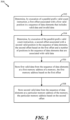
- the compressed memory data vector 110 is shown after completion of the store operations described above.
- Each valid data value of the data vectors 132, 134, 136 may be stored at contiguous memory addresses of the compressed memory data vector 110.
- invalid data may be separated from the sparse data vectors 132, 134, 136 to generate the compressed memory data vector 110 having valid data at each memory address.
- the processor 150 may fetch the compressed memory data vector 110 from the memory 102 to process valid data as opposed to processing valid data and invalid data, which may result in inefficient use of the processor 104.
- the offset determination circuitry 146 may be configured to determine (e.g., count) an offset for each data vector 132, 134, 136 with respect to the compressed memory data vector 110. For example, the offset determination circuitry 146 may determine a count (e.g., a parallel-prefix valid count) of write enables for each data vector 132, 134, 136. The offset for each data vector 132, 134, 136 may be based on the parallel-prefix valid count.
- the "offset" for a particular data vector is the first sequential memory address of the compressed memory data vector 110 where valid data associated with the particular data vector is stored.
- the offset determination circuity 146 may generate multiple offsets 160 corresponding to the data vectors 132-136, including a first offset 162 of the first data vector 132, a second offset 164 of the second data vector 134, and a third offset 166 of the third data vector 136. For example, as described further with reference to FIG.
- the first offset 162 may have a value of "1" to indicate that valid data of the first data vector 132 begins at the first memory address 111 of the compressed memory data vector 110
- the second offset 164 may have a value of "4" to indicate that valid data of the second data vector 134 begins at the fourth memory address 114
- the third offset 166 may have a value of "7" to indicate that the valid data of the third data vector 136 begins at the seventh memory address 117 of the of the compressed memory data vector 110.
- the processor 104 may execute the parallel-prefix valid count instruction 108 to determine the offset.
- FIG. 4 a chart 400 for identifying the offset for each data vector 132, 134, 136 is shown in FIG. 4 .
- memory address "0" may be used as the base address for the first data vector 132.
- a parallel prefix count of the first data vector 132 may increase (from zero to one) in response to an enable (e.g., a write enable) associated with storing valid data value "A" at the compressed memory data vector 110.
- an enable e.g., a write enable
- the memory address also increases.
- the memory address increases from memory address "0" to memory address "1" (e.g., the first memory address 111).
- the offset 162 for the first data vector 132 with respect to the compressed memory data vector 110 is the first memory address 111 and may be stored as having an offset value of "1" to indicate the first memory address 111. In other embodiments, the offset 162 may be stored having another offset value that indicates the first memory address 111, such as an offset value of "0" in a zero-based indexing implementation.
- the parallel prefix count may increase (from one to two) in response to an enable associated with storing valid data value "B" at the second memory address 112 of the compressed memory data vector 110.
- the parallel prefix count may also increase (from two to three) in response to an enable associated with storing valid data value "C” at the third memory address 113 of compressed memory data vector 110.
- the address of the last valid data value stored may be used as the based for a new data vector. Because memory address "3" (e.g., the third memory address 113) is the address of the last data value (e.g., valid data value "C") stored, the third memory address 113 may be used as the base for the second data vector 134.
- the corresponding memory address may be the offset 164 for the second data vector 134.
- the offset 164 for the second data vector 134 with respect to the compressed memory data vector 110 is the fourth memory address 114 and may be represented as having an offset value of "4" (or "3" in a zero-based indexing implementation).
- the offset 166 for the third data vector 136 with respect to the compressed memory data vector 110 is the seventh memory address 117 and may be represented as having an offset value of "7" (or "6" in a zero-based indexing implementation).
- the offsets may be used to map data in the memory 102 to the data vectors 132, 134, 136.
- the processor 104 may determine that the first, second, and third memory addresses 111, 112, 113 include data associated with the first data vector 132 if the offset 162 of the first data vector 132 is the first memory address 111 and the offset 164 of the second data vector 134 is the fourth memory address 114.
- the processor 104 may determine that the fourth, fifth, and sixth memory addresses 114, 115, 116 include data associated with the second data vector 134 if the offset 164 of the second data vector 134 is the fourth memory address 114 and the offset 166 of the third data vector 136 is the seventh memory address 117.
- the fetch circuity 150 may be configured to fetch the data stored in the compressed memory data vector 110.
- the fetch circuitry 150 may provide the compressed memory data vector 110 to the SIMD processing pipeline 152. Because each memory address of the compressed memory data vector 110 includes valid data values, the processing components and hardware in the SIMD processing pipeline 152 may be efficiently used. For example, processing components in the SIMD processing pipeline 152 may be used on valid data values as opposed to being used for invalid data values.
- the techniques described with respect to FIGS. 1-4 may improve processing efficiency by reducing the amount of invalid data values that are processed by the SIMD processing pipeline 152.
- the fetch circuitry 150 may provide valid data values (as opposed to valid and invalid data values) to the SIMD processing pipeline 152.
- a relatively simple addressing scheme may be achieved by tracking the parallel-prefix valid count for each data vector 132, 134, 136 during the storage process. For example, the processor 104 may identify which data values and/or memory addresses correspond to each data vector 132, 134, 136 based on the parallel-prefix valid count.
- the parallel-prefix valid count instruction 108 may be used during compression of sparse data from the multiple data vectors 132-136 to a dense data arrangement in the compressed memory data vector 110.
- the parallel-prefix valid count instruction 108 may be used during decompression of the data from the compressed memory data vector 110 to a sparse data arrangement in the data vectors 132-136.
- the data in the compressed memory data vector 110 may be processed by the SIMD processing pipeline 152 to generate modified data in the compressed memory data vector 110.
- the modified data may be written back to the corresponding positions of the data vectors 132-136 to overwrite the original valid data with the modified data.
- a contiguous offset or address for each valid position in the data vectors 132-136 may be computed using the parallel-prefix valid count instruction 108 with accumulation from the last count of the prior vector, as described in FIG. 4 .
- a load/gather may be performed to load the data from each address or offset in the compressed memory data vector 110 into the valid data positions of the data vectors 132-136 based on the results of the parallel-prefix valid count instruction 108.
- the parallel-prefix valid count instruction 108 may be used during data compression operations and also during data decompression operations.
- FIG. 5 a flowchart of a method 500 for storing data at contiguous memory addresses is shown.
- the method 500 may be performed using the system 100 of FIG. 1 .
- the method 500 includes determining, by execution of a parallel-prefix valid count instruction, a first offset associated with a first valid position in a sequence of data elements that includes valid data and invalid data, at 502.
- the SIMD processor 104 may execute the parallel-prefix valid count instruction 108 to determine the first offset 162 of the first data vector 132.
- the method 500 also includes determining, by execution of the parallel-prefix valid count instruction, a second offset associated with a second valid position in the sequence of data elements, at 504.
- the second offset may be based on the first offset and a number of positions in the sequence of data elements that are associated with valid data.
- the SIMD processor 104 may execute the parallel-prefix valid count instruction 108 to determine the second offset 164 of the second data vector 134.
- the second offset may be computed by adding the number of positions in the first data vector 132 that are associated with valid data to the first offset 162.
- the method 500 also includes storing first valid data from the first data vector at a first memory address of a memory, at 506.
- the first memory address may be based on the first offset. For example, referring to FIG. 1 , in response to a determination that valid data value "A" is located at "Position 1" of the first data vector 132, the memory storage circuitry 140 may enable the write circuitry 144.
- the write circuitry 144 may store valid data value "A" at the first memory address 111 in response to being enabled. For example, the write circuitry 144 may execute the scatter instruction 106 to store valid data value "A" at the first memory address 111.
- the method 500 also includes storing second valid data from the second data vector at a particular memory address of the memory, at 508.
- the particular memory address may be based on the second offset.
- the memory storage circuitry 140 may enable the write circuitry 144.
- the write circuitry 144 may store valid data value "D" at the fourth memory address 114 (e.g., the "second memory address” according to the method 500) in response to being enabled.
- the write circuitry 144 may execute the scatter instruction 106 to store valid data value "D" at the fourth memory address 114.
- the method 500 may include storing additional valid data from the first data vector at additional sequential memory addresses that are contiguous to the first memory address of the memory.
- the particular memory address (where the second valid data is stored) may be contiguous to a last memory address of the additional sequential memory address.
- the first valid data and the second valid data may be stored in parallel. For example, storing the second valid data in parallel with the first valid data includes storing the first valid data during a first time period (e.g., during a single clock cycle of the SIMD processor 104) and concurrently storing the second valid data during the first time period.
- the first memory address and the particular memory address may be memory addresses of a compressed memory data vector (e.g., the compressed memory data vector 110).
- the method 500 may also include fetching data stored at the compressed memory data vector and processing the data stored at the compressed memory data vector in response to fetching the data stored at the compressed memory data vector.
- a "decompression" operation may be performed after processing the data stored at the compressed memory data vector.
- the parallel-prefix valid count instruction may be executed to determine offsets that map positions of processed data in contiguous memory to positions of valid data in a sparse sequence of data.
- the processed data may then be loaded from the contiguous memory to the positions of valid data in the sparse sequence of data.
- the compressed arrangement of processed data in the contiguous memory may be decompressed to a sparse arrangement of the processed data based on positions of valid data in the data vectors 132-136.
- the method 500 of FIG. 5 may improve processing efficiency by reducing the amount of invalid data values that are processed by the SIMD processing pipeline 152.
- the fetch circuitry 150 may provide valid data values (as opposed to valid and invalid data values) to the SIMD processing pipeline 152.
- a relatively simple addressing scheme may be achieved by tracking the parallel-prefix valid count for each data vector 132, 134, 136 during the storage process. For example, the processor 104 may identify which data values and/or memory addresses correspond to each data vector 132, 134, 136 based on the parallel-prefix valid count.
- the electronic device 600 may correspond to a mobile device (e.g., a cellular telephone), as an illustrative example.
- the electronic device 600 may correspond to a computer (e.g., a server, a laptop computer, a tablet computer, or a desktop computer), a wearable electronic device (e.g., a personal camera, a head-mounted display, or a watch), a vehicle control system or console, a home appliance, a set top box, an entertainment unit, a navigation device, a personal digital assistant (PDA), a television, a monitor, a tuner, a radio (e.g., a satellite radio), a music player (e.g., a digital music player or a portable music player), a video player (e.g., a digital video player, such as a digital video disc (DVD) player or a portable digital video player), a robot, a healthcare device, another electronic
- a computer e.g., a server, a laptop computer, a
- the electronic device 600 includes the processor 104, such as a digital signal processor (DSP), a central processing unit (CPU), a graphics processing unit (GPU), another processing device, or a combination thereof.
- the processor 104 includes the one or more registers 130, the memory storage circuitry 140, the fetch circuitry 150, and the SIMD processing pipeline 152.
- the one or more registers 110 store the first data vector 132, the second data vector 134, and the third data vector 136.
- the memory storage circuitry 140 includes the data vector analysis circuitry 142, the write circuitry 144, and the offset determination circuitry 146.
- the processor 104 may operate in a substantially similar manner as described with respect to FIG. 1 .
- the electronic device 600 may further include the memory 102.
- the memory 102 may be coupled to or integrated within the processor 104.
- the memory 102 may include random access memory (RAM), magnetoresistive random access memory (MRAM), flash memory, read-only memory (ROM), programmable read-only memory (PROM), erasable programmable read-only memory (EPROM), electrically erasable programmable read-only memory (EEPROM), one or more registers, a hard disk, a removable disk, a compact disc read-only memory (CD-ROM), another storage device, or a combination thereof.
- the memory 102 may store the scatter instruction 106, the parallel-prefix valid count instruction 108, and one or more other instructions 668 executable by the processor 610.
- the processor 104 may execute the scatter instruction 106 to store valid data values (of the data vectors 132, 134, 136) in the compressed memory data vector 110.
- the processor 104 may also execute the parallel-prefix valid count instruction 108 to determine the offset for each data vector 132, 134, 136 with respect to the compressed memory data vector 110.
- the processor 104 may also execute the one or more other instructions 668 to perform the method 500 of FIG. 5 .
- FIG. 6 also shows a display controller 626 that is coupled to the processor 104 and to a display 628.
- a coder/decoder (CODEC) 634 can also be coupled to the processor 104.
- a speaker 636 and a microphone 638 can be coupled to the CODEC 634.
- FIG. 6 also indicates that a wireless interface 640, such as a wireless controller and/or a transceiver, can be coupled to the processor 104 and to an antenna 642.
- the processor 104, the display controller 626, the memory 102, the CODEC 634, and the wireless interface 640 are included in a system-in-package or system-on-chip device 622.
- an input device 630 and a power supply 644 may be coupled to the system-on-chip device 622.
- the display 628, the input device 630, the speaker 636, the microphone 638, the antenna 642, and the power supply 644 are external to the system-on-chip device 622.
- each of the display 628, the input device 630, the speaker 636, the microphone 638, the antenna 642, and the power supply 644 can be coupled to a component of the system-on-chip device 622, such as to an interface or to a controller.
- a computer-readable medium e.g., the memory 102 stores instructions that are executable by a processor (e.g., the processor 104) to perform operations.
- the operations include storing first valid data at a first memory address of a memory.
- the first valid data may be located at a first particular position of a first data vector that includes valid data and invalid data.
- the first particular position may be associated with valid data.
- the operations also include determining whether the first data vector includes another position associated with valid data. If the first data vector includes another position associated with valid data, the operations include storing the valid data located at the other position at a second memory address that is contiguous to the first memory address.
- the operations also include storing second valid data at the second memory address if the first data vector does not include another position associated with valid data.
- the second data may be located at a second particular position of a second data vector that includes valid data and invalid data.
- the second particular position may be associated with valid data.
- an apparatus includes means for determining a first offset associated with a first valid position in a sequence of data elements via execution of a parallel-prefix valid count instruction.
- the sequence of data elements may include valid data and invalid data.
- the means for determining the first offset may include the memory storage circuitry 140 of FIGS. 1 and 6 , the data vector analysis circuitry 142 of FIGS. 1 and 6 , the offset determination circuitry 146 of FIGS. 1 and 6 , the processor 104 of FIGS. 1 and 6 , one or more other devices, circuits, modules, or any combination thereof.
- the apparatus may also include means for determining a second offset associated with a second valid position in the sequence of data elements via execution of the parallel-prefix valid count instruction.
- the second offset may be based on the first offset and a number of positions in the sequence of data elements that are associated with valid data.
- the means for determining the second offset may include the memory storage circuitry 140 of FIGS. 1 and 6 , the data vector analysis circuitry 142 of FIGS. 1 and 6 , the offset determination circuitry 146 of FIGS. 1 and 6 , the processor 104 of FIGS. 1 and 6 , one or more other devices, circuits, modules, or any combination thereof.
- the foregoing disclosed devices and functionalities may be designed and represented using computer files (e.g. RTL, GDSII, GERBER, etc.).
- the computer files may be stored on computer-readable media. Some or all such files may be provided to fabrication handlers who fabricate devices based on such files. Resulting products include wafers that are then cut into die and packaged into integrated circuits (or "chips"). The chips are then employed in electronic devices, such as the electronic device 600 of FIG. 6 .
- a software module may reside in random access memory (RAM), flash memory, read-only memory (ROM), programmable read-only memory (PROM), erasable programmable read-only memory (EPROM), electrically erasable programmable read-only memory (EEPROM), registers, hard disk, a removable disk, a compact disc read-only memory (CD-ROM), or any other form of storage medium known in the art.
- An exemplary non-transitory (e.g. tangible) storage medium is coupled to the processor such that the processor can read information from, and write information to, the storage medium.
- the storage medium may be integral to the processor.
- the processor and the storage medium may reside in an application-specific integrated circuit (ASIC).
- ASIC application-specific integrated circuit
- the ASIC may reside in a computing device or a user terminal.
- the processor and the storage medium may reside as discrete components in a computing device or user terminal.
Landscapes
- Engineering & Computer Science (AREA)
- Theoretical Computer Science (AREA)
- Software Systems (AREA)
- Physics & Mathematics (AREA)
- General Engineering & Computer Science (AREA)
- General Physics & Mathematics (AREA)
- Mathematical Physics (AREA)
- Complex Calculations (AREA)
- Advance Control (AREA)
- Executing Machine-Instructions (AREA)
- Communication Control (AREA)
Description
- The present disclosure is generally related to data storage.
- Advances in technology have resulted in more powerful computing devices. For example, computing devices such as laptop and desktop computers and servers, as well as wireless computing devices such as portable wireless telephones, personal digital assistants (PDAs), and paging devices, have improved computing capabilities and are able to perform increasingly complex operations. Increased computing capabilities have also enhanced device capabilities in various other applications. For example, vehicles may include processing devices to enable global positioning system operations or other location operations, self-driving operations, interactive communication and entertainment operations, etc. Other examples include household appliances, security cameras, metering equipment, etc., that also incorporate computing devices to enable enhanced functionality, such as communication using the internet-of things.
- A computing device may include a processor that is operable to process one or more sparse data vectors. As used herein, a "sparse data vector" is a vector of data that includes data elements having invalid data (e.g., "don't care" data values, default data values, null data values, or zero data values) and data elements having valid data (e.g., data values "of interest"). Invalid data in a data vector leads to inefficient computation and storage. For example, because sparse data vectors include data elements having invalid data items that do not have to be processed, components (e.g., hardware) included in the processor may be inefficiently used by processing the invalid data.
- One technique for improving hardware usage efficiency includes compressing a sparse data vector within a processing pipeline of the processor to generate a compressed data vector. To generate the compressed data vector, the processor may shift data (within the processing pipeline of the processor) such that data elements having valid data are adjacent to one another and data elements having invalid data are adjacent to one another. However, generating compressed data vectors within the processing pipeline may result in a relatively large number of data vectors with complex addressing schemes. Additionally, generating compressed data vectors within the processing pipeline may result in increased hardware costs.
- The invention is defined by the subject-matter of the independent claims. Preferred embodiments are defined in the dependent claims.
-
-
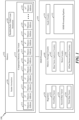
FIG. 1 is a diagram of a system that is operable to store data at contiguous memory addresses; -
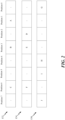
FIG. 2 illustrates sparse data vectors that include valid data and invalid data; -
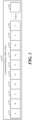
FIG. 3 illustrates a compressed memory data vector; -
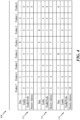
FIG. 4 illustrates a chart for identifying an offset of valid data values in a compressed memory data vector; -
FIG. 5 illustrates a method for storing data at contiguous memory addresses; and -
FIG. 6 is a diagram of an electronic device that includes components operable to store data at contiguous memory addresses. - Referring to
FIG. 1 , asystem 100 that is operable to store data at contiguous memory addresses is shown. Thesystem 100 may be implemented within a mobile phone, a personal digital assistant (PDA), an entertainment unit, a navigation device, a music player, a video player, a digital video player, a digital video disc (DVD) player, or any other device. - The
system 100 includes amemory 102 that is coupled to aprocessor 104. According to one embodiment theprocessor 104 includes a single-instruction-multiple-data (SIMD) processor. Thememory 102 may be a non-transitory computer-readable medium that includes instructions that are executable by theprocessor 104. For example, thememory 102 includes ascatter instruction 106 that is executable by theprocessor 104 and a parallel-prefixvalid count instruction 108 that is executable by theprocessor 104. - The
memory 102 also includes a compressedmemory data vector 110. As described below, valid data (as opposed to invalid data) from different sparse data vectors may be stored at the compressedmemory data vector 110 to generate a "compressed data vector" in thememory 102. The compressedmemory data vector 110 includes a plurality of contiguous memory addresses. To illustrate, the compressedmemory data vector 110 includes afirst memory address 111, asecond memory address 112 that is contiguous to thefirst memory address 111, athird memory address 113 that is contiguous to thesecond memory address 112, afourth memory address 114 that is contiguous to thethird memory address 113, afifth memory address 115 that is contiguous to thefourth memory address 114, asixth memory address 116 that is contiguous to thefifth memory address 115, aseventh memory address 117 that is contiguous to thesixth memory address 116, aneighth memory address 118 that is contiguous to theseventh memory address 117, aninth memory address 119 that is contiguous to theeighth memory address 118, atenth memory address 120 that is contiguous to theninth memory address 119, etc. - In
FIG. 1 , the compressedmemory data vector 110 includes sixteen memory addresses. For example, the compressedmemory data vector 110 includes asixteenth memory address 122 that is contiguous to a fifteenth memory address (not shown). However, in other embodiments, the compressedmemory data vector 110 may include additional (or fewer) contiguous memory addresses. As a non-limiting example, the compressedmemory data vector 110 may include thirty-two contiguous memory addresses. - The
processor 104 includes one ormore registers 130,memory storage circuitry 140,fetch circuitry 150, and aSIMD processing pipeline 152. Although the one ormore registers 130 are shown to be included in theprocessor 104, in other embodiments, the one ormore registers 130 may be separate from (and accessible to) theprocessor 104. In other embodiments, theprocessor 104 may include additional (or fewer) components. As a non-limiting example, in other embodiments, theprocessor 104 may also include one or more arithmetic logic units (ALUs), one or more application-specific execution units, etc. Although theprocessor 104 is shown to include thememory storage circuitry 140, thefetch circuitry 150, and theSIMD processing pipeline 152, in other embodiments, operations of eachcomponent - The one or
more registers 130 may store afirst data vector 132, asecond data vector 134, and athird data vector 136. A "sequence of data elements" may include the data elements stored in thedata vectors data vectors more registers 130, in other embodiments, the one ormore registers 130 may include additional (or fewer) data vectors. Eachdata vector data vector data vectors - Referring to
FIG. 2 , thedata vectors data vector Position 0" to "Position 7"). According to one embodiment, each position may correspond to an "array position". Although eachdata vector data vector data vector - According to
FIG. 2 , thefirst data vector 132 includes three valid data values and five invalid data values. For example, "Position 1" of thefirst data vector 132 stores valid data value "A", "Position 3" of thefirst data vector 132 stores valid data value "B", and "Position 6" of thefirst data vector 132 stores valid data value "C". The other positions of thefirst data vector 132 store invalid data values. Thesecond data vector 134 also includes three valid data values and five invalid data values. For example, "Position 2" of thesecond data vector 134 stores valid data value "D", "Position 3" of thesecond data vector 134 stores valid data value "E", and "Position 6" of thesecond data vector 134 stores valid data value "F". The other positions of thesecond data vector 134 store invalid data values. Thethird data vector 136 includes four valid data values and four invalid data values. For example, "Position 0" of thethird data vector 136 stores valid data value "G", "Position 4" of thethird data vector 136 stores valid data value "H", "Position 5" of thethird data vector 136 stores valid data value "I", and "Position 7" of thethird data vector 136 stores valid data value "J". The other positions of thethird data vector 136 store invalid data values. - Referring back to
FIG. 1 , thememory storage circuitry 140 includes datavector analysis circuitry 142, writecircuitry 144, and offsetdetermination circuitry 146. The datavector analysis circuitry 142 may be configured to determine whether thefirst data vector 132 includes positions having valid data. For example, the datavector analysis circuitry 142 may determine that valid data value "A" is located at "Position 1" of the first data vector 132 (e.g., the first sequential position having valid data). Thewrite circuitry 144 may be configured to write (e.g., store) valid data values (in parallel) at the contiguous memory addresses of the compressedmemory data vector 110. For example, in response to a determination that valid data value "A" is located at "Position 1" of thefirst data vector 132, thememory storage circuitry 140 may enable thewrite circuitry 144. Thewrite circuitry 144 may store valid data value "A" at thefirst memory address 111 in response to being enabled. For example, thewrite circuitry 144 may execute the scatter instruction 106 (e.g., a vector store instruction) to store valid data value "A" at thefirst memory address 111. - After valid data value "A" is stored at the
first memory address 111, the datavector analysis circuity 142 may determine whether thefirst data vector 132 includes another position having valid data. For example, the datavector analysis circuitry 142 may determine that valid data value "B" is located at "Position 3" of the first data vector 132 (e.g., the next sequential position having valid data). In response to a determination that valid data value "B" is located at "Position 3" of thefirst data vector 132, thememory storage circuitry 140 may enable thewrite circuitry 144. Thewrite circuitry 144 may store valid data value "B" at the second memory address 112 (e.g., a contiguous memory address of the first memory address 111) in response to being enabled. For example, thewrite circuitry 144 may execute thescatter instruction 106 to store valid data value "B" at thesecond memory address 112. - After valid data value "B" is stored at the
second memory address 112, the datavector analysis circuity 142 may determine whether thefirst data vector 132 includes another position having valid data. For example, the datavector analysis circuitry 142 may determine that valid data value "C" is located at "Position 6" of the first data vector 132 (e.g., the next sequential position having valid data). In response to a determination that valid data value "C" is located at "Position 6" of thefirst data vector 132, thememory storage circuitry 140 may enable thewrite circuitry 144. Thewrite circuitry 144 may store valid data value "C" at the third memory address 113 (e.g., a contiguous memory address of the second memory address 112) in response to being enabled. For example, thewrite circuitry 144 may execute thescatter instruction 106 to store valid data value "C" at thethird memory address 113. Thus, the invalid data values of thefirst data vector 132 may be bypassed and the valid data values of thefirst data vector 132 may be stored at contiguous memory addresses in thememory 102. - After valid data value "C" is stored at the
third memory address 113, the datavector analysis circuity 142 may determine whether thefirst data vector 132 includes another position having valid data. In response to a determination that thefirst data vector 132 does not include another position having valid data, the datavector analysis circuitry 142 may determine whether thesecond data vector 134 includes a position having valid data. For example, the datavector analysis circuitry 142 may determine that valid data value "D" is located at "Position 2" of the second data vector 134 (e.g., the first sequential position having valid data). In response to a determination that valid data value "D" is located at "Position 2" of thesecond data vector 134, thememory storage circuitry 140 may enable thewrite circuitry 144. Thewrite circuitry 144 may store valid data value "D" at the fourth memory address 114 (e.g., a contiguous memory address of the third memory address 113) in response to being enabled. For example, thewrite circuitry 144 may execute thescatter instruction 106 to store valid data value "D" at thefourth memory address 114. - After valid data value "D" is stored at the
fourth memory address 114, the datavector analysis circuity 142 may determine whether thesecond data vector 134 includes another position having valid data. For example, the datavector analysis circuitry 142 may determine that valid data value "E" is located at "Position 3" of the second data vector 134 (e.g., the next sequential position having valid data). In response to a determination that valid data value "E" is located at "Position 3" of thesecond data vector 134, thememory storage circuitry 140 may enable thewrite circuitry 144. Thewrite circuitry 144 may store valid data value "E" at the fifth memory address 115 (e.g., a contiguous memory address of the fourth memory address 114) in response to being enabled. For example, thewrite circuitry 144 may execute thescatter instruction 106 to store valid data value "E" at thefifth memory address 115. - After valid data value "E" is stored at the
fifth memory address 115, the datavector analysis circuity 142 may determine whether thesecond data vector 134 includes another position having valid data. For example, the datavector analysis circuitry 142 may determine that valid data value "F" is located at "Position 6" of the second data vector 134 (e.g., the next sequential position having valid data). In response to a determination that valid data value "F" is located at "Position 6" of thesecond data vector 134, thememory storage circuitry 140 may enable thewrite circuitry 144. Thewrite circuitry 144 may store valid data value "F" at the sixth memory address 116 (e.g., a contiguous memory address of the fifth memory address 115) in response to being enabled. For example, thewrite circuitry 144 may execute thescatter instruction 106 to store valid data value "F" at thesixth memory address 116. Thus, the invalid data values of thesecond data vector 134 may be bypassed and the valid data values of thesecond data vector 134 may be stored at contiguous memory addresses in thememory 102. - After valid data value "F" is stored at the
sixth memory address 116, the datavector analysis circuity 142 may determine whether thesecond data vector 134 includes another position having valid data. In response to a determination that thesecond data vector 134 does not include another position having valid data, the datavector analysis circuitry 142 may determine whether thethird data vector 136 includes a position having valid data. For example, the datavector analysis circuitry 142 may determine that valid data value "G" is located at "Position 1" of the third data vector 136 (e.g., the first sequential position having valid data). In response to a determination that valid data value "G" is located at "Position 1" of thethird data vector 136, thememory storage circuitry 140 may enable thewrite circuitry 144. Thewrite circuitry 144 may store valid data value "G" at the seventh memory address 117 (e.g., a contiguous memory address of the sixth memory address 116) in response to being enabled. For example, thewrite circuitry 144 may execute thescatter instruction 106 to store valid data value "G" at theseventh memory address 117. - After valid data value "G" is stored at the
seventh memory address 117, the datavector analysis circuity 142 may determine whether thethird data vector 136 includes another position having valid data. For example, the datavector analysis circuitry 142 may determine that valid data value "H" is located at "Position 4" of the third data vector 136 (e.g., the next sequential position having valid data). In response to a determination that valid data value "H" is located at "Position 4" of thethird data vector 136, thememory storage circuitry 140 may enable thewrite circuitry 144. Thewrite circuitry 144 may store valid data value "H" at the eighth memory address 118 (e.g., a contiguous memory address of the seventh memory address 117) in response to being enabled. For example, thewrite circuitry 144 may execute thescatter instruction 106 to store valid data value "H" at theeighth memory address 118. - After valid data value "H" is stored at the
eighth memory address 118, the datavector analysis circuity 142 may determine whether thethird data vector 136 includes another position having valid data. For example, the datavector analysis circuitry 142 may determine that valid data value "I" is located at "Position 5" of the third data vector 136 (e.g., the next sequential position having valid data). In response to a determination that valid data value "I" is located at "Position 5" of thethird data vector 136, thememory storage circuitry 140 may enable thewrite circuitry 144. Thewrite circuitry 144 may store valid data value "I" at the ninth memory address 119 (e.g., a contiguous memory address of the eighth memory address 118) in response to being enabled. For example, thewrite circuitry 144 may execute thescatter instruction 106 to store valid data value "I" at theninth memory address 119. - After valid data value "J" is stored at the
ninth memory address 119, the datavector analysis circuity 142 may determine whether thethird data vector 136 includes another position having valid data. For example, the datavector analysis circuitry 142 may determine that valid data value "J" is located at "Position 7" of the third data vector 136 (e.g., the next sequential position having valid data). In response to a determination that valid data value "J" is located at "Position 7" of thethird data vector 136, thememory storage circuitry 140 may enable thewrite circuitry 144. Thewrite circuitry 144 may store valid data value "J" at the tenth memory address 120 (e.g., a contiguous memory address of the ninth memory address 119) in response to being enabled. For example, thewrite circuitry 144 may execute thescatter instruction 106 to store valid data value "J" at thetenth memory address 120. Thus, the invalid data values of thethird data vector 136 may be bypassed and the valid data values of thethird data vector 136 may be stored at contiguous memory addresses in thememory 102. - Similar operations may be performed to store additional valid data values to the compressed
memory data vector 110 of thememory 102. Referring toFIG. 3 , the compressedmemory data vector 110 is shown after completion of the store operations described above. Each valid data value of thedata vectors memory data vector 110. Thus, invalid data may be separated from thesparse data vectors memory data vector 110 having valid data at each memory address. As described below, theprocessor 150 may fetch the compressedmemory data vector 110 from thememory 102 to process valid data as opposed to processing valid data and invalid data, which may result in inefficient use of theprocessor 104. - Referring back to
FIG. 1 , the offsetdetermination circuitry 146 may be configured to determine (e.g., count) an offset for eachdata vector memory data vector 110. For example, the offsetdetermination circuitry 146 may determine a count (e.g., a parallel-prefix valid count) of write enables for eachdata vector data vector memory data vector 110 where valid data associated with the particular data vector is stored. The offsetdetermination circuity 146 may generate multiple offsets 160 corresponding to the data vectors 132-136, including a first offset 162 of thefirst data vector 132, a second offset 164 of thesecond data vector 134, and a third offset 166 of thethird data vector 136. For example, as described further with reference toFIG. 4 , the first offset 162 may have a value of "1" to indicate that valid data of thefirst data vector 132 begins at thefirst memory address 111 of the compressedmemory data vector 110, the second offset 164 may have a value of "4" to indicate that valid data of thesecond data vector 134 begins at thefourth memory address 114, and the third offset 166 may have a value of "7" to indicate that the valid data of thethird data vector 136 begins at theseventh memory address 117 of the of the compressedmemory data vector 110. According to one embodiment, theprocessor 104 may execute the parallel-prefixvalid count instruction 108 to determine the offset. - To illustrate, a
chart 400 for identifying the offset for eachdata vector FIG. 4 . According to thechart 400, memory address "0" may be used as the base address for thefirst data vector 132. A parallel prefix count of thefirst data vector 132 may increase (from zero to one) in response to an enable (e.g., a write enable) associated with storing valid data value "A" at the compressedmemory data vector 110. Each time the parallel prefix count increases, the memory address also increases. Thus, under the "Position 1" column in thechart 400, the memory address increases from memory address "0" to memory address "1" (e.g., the first memory address 111). Thus, the offset 162 for thefirst data vector 132 with respect to the compressedmemory data vector 110 is thefirst memory address 111 and may be stored as having an offset value of "1" to indicate thefirst memory address 111. In other embodiments, the offset 162 may be stored having another offset value that indicates thefirst memory address 111, such as an offset value of "0" in a zero-based indexing implementation. - The parallel prefix count may increase (from one to two) in response to an enable associated with storing valid data value "B" at the
second memory address 112 of the compressedmemory data vector 110. The parallel prefix count may also increase (from two to three) in response to an enable associated with storing valid data value "C" at thethird memory address 113 of compressedmemory data vector 110. As described above, the address of the last valid data value stored may be used as the based for a new data vector. Because memory address "3" (e.g., the third memory address 113) is the address of the last data value (e.g., valid data value "C") stored, thethird memory address 113 may be used as the base for thesecond data vector 134. When the parallel-prefix count of thesecond data vector 134 increases (from zero to one), the corresponding memory address may be the offset 164 for thesecond data vector 134. Thus, the offset 164 for thesecond data vector 134 with respect to the compressedmemory data vector 110 is thefourth memory address 114 and may be represented as having an offset value of "4" (or "3" in a zero-based indexing implementation). In a similar manner, according to thechart 400, the offset 166 for thethird data vector 136 with respect to the compressedmemory data vector 110 is theseventh memory address 117 and may be represented as having an offset value of "7" (or "6" in a zero-based indexing implementation). - Referring back to
FIG. 1 , the offsets (determined by the offset determination circuitry 146) may be used to map data in thememory 102 to thedata vectors processor 104 may determine that the first, second, and third memory addresses 111, 112, 113 include data associated with thefirst data vector 132 if the offset 162 of thefirst data vector 132 is thefirst memory address 111 and the offset 164 of thesecond data vector 134 is thefourth memory address 114. Similarly, theprocessor 104 may determine that the fourth, fifth, and sixth memory addresses 114, 115, 116 include data associated with thesecond data vector 134 if the offset 164 of thesecond data vector 134 is thefourth memory address 114 and the offset 166 of thethird data vector 136 is theseventh memory address 117. - After the data values are stored in the compressed
memory data vector 110, the fetchcircuity 150 may be configured to fetch the data stored in the compressedmemory data vector 110. The fetchcircuitry 150 may provide the compressedmemory data vector 110 to theSIMD processing pipeline 152. Because each memory address of the compressedmemory data vector 110 includes valid data values, the processing components and hardware in theSIMD processing pipeline 152 may be efficiently used. For example, processing components in theSIMD processing pipeline 152 may be used on valid data values as opposed to being used for invalid data values. - The techniques described with respect to
FIGS. 1-4 may improve processing efficiency by reducing the amount of invalid data values that are processed by theSIMD processing pipeline 152. By storing valid data values at contiguous addresses in thememory 102, the fetchcircuitry 150 may provide valid data values (as opposed to valid and invalid data values) to theSIMD processing pipeline 152. Additionally, a relatively simple addressing scheme may be achieved by tracking the parallel-prefix valid count for eachdata vector processor 104 may identify which data values and/or memory addresses correspond to eachdata vector - As described with reference to
FIGS. 1-4 , the parallel-prefixvalid count instruction 108 may be used during compression of sparse data from the multiple data vectors 132-136 to a dense data arrangement in the compressedmemory data vector 110. Alternatively, or in addition, the parallel-prefixvalid count instruction 108 may be used during decompression of the data from the compressedmemory data vector 110 to a sparse data arrangement in the data vectors 132-136. For example, after compressing the data into the compressedmemory data vector 110, the data in the compressedmemory data vector 110 may be processed by theSIMD processing pipeline 152 to generate modified data in the compressedmemory data vector 110. The modified data may be written back to the corresponding positions of the data vectors 132-136 to overwrite the original valid data with the modified data. In a decompression operation, a contiguous offset or address for each valid position in the data vectors 132-136 may be computed using the parallel-prefixvalid count instruction 108 with accumulation from the last count of the prior vector, as described inFIG. 4 . A load/gather may be performed to load the data from each address or offset in the compressedmemory data vector 110 into the valid data positions of the data vectors 132-136 based on the results of the parallel-prefixvalid count instruction 108. Thus, the parallel-prefixvalid count instruction 108 may be used during data compression operations and also during data decompression operations. - Referring to
FIG. 5 , a flowchart of amethod 500 for storing data at contiguous memory addresses is shown. Themethod 500 may be performed using thesystem 100 ofFIG. 1 . - The
method 500 includes determining, by execution of a parallel-prefix valid count instruction, a first offset associated with a first valid position in a sequence of data elements that includes valid data and invalid data, at 502. For example, referring toFIG. 1 , theSIMD processor 104 may execute the parallel-prefixvalid count instruction 108 to determine the first offset 162 of thefirst data vector 132. - The
method 500 also includes determining, by execution of the parallel-prefix valid count instruction, a second offset associated with a second valid position in the sequence of data elements, at 504. The second offset may be based on the first offset and a number of positions in the sequence of data elements that are associated with valid data. For example, referring toFIG. 1 , theSIMD processor 104 may execute the parallel-prefixvalid count instruction 108 to determine the second offset 164 of thesecond data vector 134. According to one embodiment, the second offset may be computed by adding the number of positions in thefirst data vector 132 that are associated with valid data to the first offset 162. - The
method 500 also includes storing first valid data from the first data vector at a first memory address of a memory, at 506. The first memory address may be based on the first offset. For example, referring toFIG. 1 , in response to a determination that valid data value "A" is located at "Position 1" of thefirst data vector 132, thememory storage circuitry 140 may enable thewrite circuitry 144. Thewrite circuitry 144 may store valid data value "A" at thefirst memory address 111 in response to being enabled. For example, thewrite circuitry 144 may execute thescatter instruction 106 to store valid data value "A" at thefirst memory address 111. - The
method 500 also includes storing second valid data from the second data vector at a particular memory address of the memory, at 508. The particular memory address may be based on the second offset. For example, referring toFIG. 1 , thememory storage circuitry 140 may enable thewrite circuitry 144. Thewrite circuitry 144 may store valid data value "D" at the fourth memory address 114 (e.g., the "second memory address" according to the method 500) in response to being enabled. For example, thewrite circuitry 144 may execute thescatter instruction 106 to store valid data value "D" at thefourth memory address 114. - According to one embodiment, the
method 500 may include storing additional valid data from the first data vector at additional sequential memory addresses that are contiguous to the first memory address of the memory. The particular memory address (where the second valid data is stored) may be contiguous to a last memory address of the additional sequential memory address. According to one embodiment of themethod 500, the first valid data and the second valid data may be stored in parallel. For example, storing the second valid data in parallel with the first valid data includes storing the first valid data during a first time period (e.g., during a single clock cycle of the SIMD processor 104) and concurrently storing the second valid data during the first time period. - According to one embodiment of the
method 500, the first memory address and the particular memory address may be memory addresses of a compressed memory data vector (e.g., the compressed memory data vector 110). Themethod 500 may also include fetching data stored at the compressed memory data vector and processing the data stored at the compressed memory data vector in response to fetching the data stored at the compressed memory data vector. - According to one embodiment of the
method 500, after processing the data stored at the compressed memory data vector, a "decompression" operation may be performed. The parallel-prefix valid count instruction may be executed to determine offsets that map positions of processed data in contiguous memory to positions of valid data in a sparse sequence of data. The processed data may then be loaded from the contiguous memory to the positions of valid data in the sparse sequence of data. Thus, the compressed arrangement of processed data in the contiguous memory may be decompressed to a sparse arrangement of the processed data based on positions of valid data in the data vectors 132-136. - The
method 500 ofFIG. 5 may improve processing efficiency by reducing the amount of invalid data values that are processed by theSIMD processing pipeline 152. By storing valid data values at contiguous addresses in thememory 102, the fetchcircuitry 150 may provide valid data values (as opposed to valid and invalid data values) to theSIMD processing pipeline 152. Additionally, a relatively simple addressing scheme may be achieved by tracking the parallel-prefix valid count for eachdata vector processor 104 may identify which data values and/or memory addresses correspond to eachdata vector - Referring to
FIG. 6 , a block diagram of anelectronic device 600 is shown. Theelectronic device 600 may correspond to a mobile device (e.g., a cellular telephone), as an illustrative example. In other embodiments, theelectronic device 600 may correspond to a computer (e.g., a server, a laptop computer, a tablet computer, or a desktop computer), a wearable electronic device (e.g., a personal camera, a head-mounted display, or a watch), a vehicle control system or console, a home appliance, a set top box, an entertainment unit, a navigation device, a personal digital assistant (PDA), a television, a monitor, a tuner, a radio (e.g., a satellite radio), a music player (e.g., a digital music player or a portable music player), a video player (e.g., a digital video player, such as a digital video disc (DVD) player or a portable digital video player), a robot, a healthcare device, another electronic device, or a combination thereof. - The
electronic device 600 includes theprocessor 104, such as a digital signal processor (DSP), a central processing unit (CPU), a graphics processing unit (GPU), another processing device, or a combination thereof. Theprocessor 104 includes the one ormore registers 130, thememory storage circuitry 140, the fetchcircuitry 150, and theSIMD processing pipeline 152. The one ormore registers 110 store thefirst data vector 132, thesecond data vector 134, and thethird data vector 136. Thememory storage circuitry 140 includes the datavector analysis circuitry 142, thewrite circuitry 144, and the offsetdetermination circuitry 146. Theprocessor 104 may operate in a substantially similar manner as described with respect toFIG. 1 . - The
electronic device 600 may further include thememory 102. Thememory 102 may be coupled to or integrated within theprocessor 104. Thememory 102 may include random access memory (RAM), magnetoresistive random access memory (MRAM), flash memory, read-only memory (ROM), programmable read-only memory (PROM), erasable programmable read-only memory (EPROM), electrically erasable programmable read-only memory (EEPROM), one or more registers, a hard disk, a removable disk, a compact disc read-only memory (CD-ROM), another storage device, or a combination thereof. Thememory 102 may store thescatter instruction 106, the parallel-prefixvalid count instruction 108, and one or moreother instructions 668 executable by the processor 610. For example, theprocessor 104 may execute thescatter instruction 106 to store valid data values (of thedata vectors memory data vector 110. Theprocessor 104 may also execute the parallel-prefixvalid count instruction 108 to determine the offset for eachdata vector memory data vector 110. Theprocessor 104 may also execute the one or moreother instructions 668 to perform themethod 500 ofFIG. 5 . -
FIG. 6 also shows adisplay controller 626 that is coupled to theprocessor 104 and to adisplay 628. A coder/decoder (CODEC) 634 can also be coupled to theprocessor 104. Aspeaker 636 and amicrophone 638 can be coupled to theCODEC 634.FIG. 6 also indicates that awireless interface 640, such as a wireless controller and/or a transceiver, can be coupled to theprocessor 104 and to anantenna 642. - In a particular example, the
processor 104, thedisplay controller 626, thememory 102, theCODEC 634, and thewireless interface 640 are included in a system-in-package or system-on-chip device 622. Further, aninput device 630 and apower supply 644 may be coupled to the system-on-chip device 622. Moreover, in a particular example, as illustrated inFIG. 6 , thedisplay 628, theinput device 630, thespeaker 636, themicrophone 638, theantenna 642, and thepower supply 644 are external to the system-on-chip device 622. However, each of thedisplay 628, theinput device 630, thespeaker 636, themicrophone 638, theantenna 642, and thepower supply 644 can be coupled to a component of the system-on-chip device 622, such as to an interface or to a controller. - In connection with the disclosed examples, a computer-readable medium (e.g., the memory 102) stores instructions that are executable by a processor (e.g., the processor 104) to perform operations. The operations include storing first valid data at a first memory address of a memory. The first valid data may be located at a first particular position of a first data vector that includes valid data and invalid data. The first particular position may be associated with valid data. The operations also include determining whether the first data vector includes another position associated with valid data. If the first data vector includes another position associated with valid data, the operations include storing the valid data located at the other position at a second memory address that is contiguous to the first memory address. The operations also include storing second valid data at the second memory address if the first data vector does not include another position associated with valid data. The second data may be located at a second particular position of a second data vector that includes valid data and invalid data. The second particular position may be associated with valid data.
- In conjunction with the described techniques, an apparatus includes means for determining a first offset associated with a first valid position in a sequence of data elements via execution of a parallel-prefix valid count instruction. The sequence of data elements may include valid data and invalid data. For example, the means for determining the first offset may include the
memory storage circuitry 140 ofFIGS. 1 and6 , the datavector analysis circuitry 142 ofFIGS. 1 and6 , the offsetdetermination circuitry 146 ofFIGS. 1 and6 , theprocessor 104 ofFIGS. 1 and6 , one or more other devices, circuits, modules, or any combination thereof. - The apparatus may also include means for determining a second offset associated with a second valid position in the sequence of data elements via execution of the parallel-prefix valid count instruction. The second offset may be based on the first offset and a number of positions in the sequence of data elements that are associated with valid data. For example, the means for determining the second offset may include the
memory storage circuitry 140 ofFIGS. 1 and6 , the datavector analysis circuitry 142 ofFIGS. 1 and6 , the offsetdetermination circuitry 146 ofFIGS. 1 and6 , theprocessor 104 ofFIGS. 1 and6 , one or more other devices, circuits, modules, or any combination thereof. - The foregoing disclosed devices and functionalities may be designed and represented using computer files (e.g. RTL, GDSII, GERBER, etc.). The computer files may be stored on computer-readable media. Some or all such files may be provided to fabrication handlers who fabricate devices based on such files. Resulting products include wafers that are then cut into die and packaged into integrated circuits (or "chips"). The chips are then employed in electronic devices, such as the
electronic device 600 ofFIG. 6 . - The steps of a method or algorithm described in connection with the implementations disclosed herein may be embodied directly in hardware, in a software module executed by a processor, or in a combination of the two. A software module may reside in random access memory (RAM), flash memory, read-only memory (ROM), programmable read-only memory (PROM), erasable programmable read-only memory (EPROM), electrically erasable programmable read-only memory (EEPROM), registers, hard disk, a removable disk, a compact disc read-only memory (CD-ROM), or any other form of storage medium known in the art. An exemplary non-transitory (e.g. tangible) storage medium is coupled to the processor such that the processor can read information from, and write information to, the storage medium. In the alternative, the storage medium may be integral to the processor. The processor and the storage medium may reside in an application-specific integrated circuit (ASIC). The ASIC may reside in a computing device or a user terminal. In the alternative, the processor and the storage medium may reside as discrete components in a computing device or user terminal.
Claims (19)
- A method for storing valid data at a plurality of contiguous memory addresses (110) at a single-instruction-multiple-data, SIMD, processor (104), the processor accessing one or more locations (130) for storing a plurality of sparse data vectors (132, 134, 136), each sparse data vector including valid data and invalid data, the method comprising:identifying a first valid data value at a first valid position in a sequence of data elements of a first sparse data vector (132) of the plurality of sparse data vectors and enabling write circuitry to store the first valid data value from the first sparse data vector at a first memory address (111) of the plurality of contiguous memory addresses (110);determining a first offset (160) associated with the first memory address (111) of the plurality of contiguous memory addresses;identifying a second valid data value at a second valid position in a sequence of data elements of a second sparse data vector (134) and enabling write circuitry to store the second valid data value at a second memory address (114) of the plurality of contiguous memory addresses;determining a second offset associated with the second memory address (114) of the plurality of contiguous memory addresses, the second offset based on the first offset and a number of positions in the sequence of data elements of the first sparse data vector (132) that are associated with valid data,wherein the first memory address (111) of the plurality of contiguous memory addresses is based on the first offset and the second memory address (114) of the plurality of contiguous memory addresses is based on the second offset.
- The method of claim 1, wherein the first offset is determined concurrently with the second offset.
- The method of claim 1, further comprising adding the number of positions in the first sparse data vector (132) that are associated with valid data to the first offset (162) to compute the second offset.
- The method of claim 1, further comprising storing additional valid data from the first sparse data vector (132) at additional sequential memory addresses (112, 113) that are contiguous to the first memory address of the memory.
- The method of claim 4, wherein the second memory address is contiguous to a last memory address of the additional sequential memory addresses.
- The method of claim 1, wherein the first valid data and the second valid data are stored concurrently.
- The method of claim 1, wherein the plurality of contiguous memory addresses form a compressed memory data vector (110).
- The method of claim 1, further comprising fetching data stored at the compressed memory data vector (110).
- The method of claim 8, further comprising processing the data stored at the compressed memory data vector (110) in response to fetching the data stored at the compressed memory data vector.
- The method of claim 9, further comprising, after processing the data stored at the compressed memory data vector (110), performing a decompression operation wherein the decompression operation comprises:determining offsets that map positions of processed data in the compressed memory data vector to positions of valid data in a sparse sequence of data; andloading the processed data from the compressed memory data vector (110) to the positions of valid data in the sparse sequence of data.
- An apparatus for storing valid data at a plurality of contiguous memory addresses (110), the apparatus comprising a memory (102) and a single-instruction-multiple-data, SIMD, processor (104), the processor being configured to access one or more locations (130) for storing a plurality of sparse data vectors (132, 134, 136), each sparse data vector including valid data and invalid data, the processor being further configured to:identify a first valid data value at a first valid position in a sequence of data elements of a first sparse data vector (132) of the plurality of sparse data vectors and enabling write circuitry to store the first valid data value from the first sparse data vector at a first memory address (111) of the plurality of contiguous memory addresses (110);determine a first offset (160) associated with the first memory address (111) of the plurality of contiguous memory addresses;
identify a second valid data value at a second valid position in a sequence of data elements of a second sparse data vector (134) and enabling write circuitry to store the second valid data value at a second memory address of the plurality of contiguous memory addresses; anddetermine a second offset associated with the second memory address (114) of the plurality of contiguous memory addresses, the second offset based on the first offset and a number of positions in the sequence of data elements of the first sparse data vector (132) that are associated with valid data, wherein the first memory address (111) of the plurality of contiguous memory addresses is based on the first offset and the second memory address (114) of the plurality of contiguous memory addresses is based on the second offset. - The apparatus of claim 11, wherein the first offset is determined concurrently with the second offset.
- The apparatus of claim 11, wherein the processor is further configured to add the number of positions in the first sparse data vector (132) that are associated with valid data to the first offset (162) to compute the second offset.
- The apparatus of claim 11, wherein the processor is further configured to store additional valid data from the first sparse data vector (132) at additional sequential memory addresses (112, 113) that are contiguous to the first memory address of the memory.
- The apparatus of claim 14, wherein the second memory address is contiguous to a last memory address of the additional sequential memory addresses.
- The apparatus of claim 11, wherein the first valid data and the second valid data are stored concurrently.
- The apparatus of claim 11, wherein the plurality of contiguous memory addresses form a compressed memory data vector (110).
- The apparatus of claim 11, wherein the processor is further configured to fetch data stored at the compressed memory data vector (110).
- The apparatus of claim 18, wherein the processor is configured to process the data stored at the compressed memory data vector (110) in response to fetching the data stored at the compressed memory data vector.
Applications Claiming Priority (2)
| Application Number | Priority Date | Filing Date | Title |
|---|---|---|---|
| US15/273,366 US10162752B2 (en) | 2016-09-22 | 2016-09-22 | Data storage at contiguous memory addresses |
| PCT/US2017/044227 WO2018057115A1 (en) | 2016-09-22 | 2017-07-27 | Data storage at contiguous memory addresses |
Publications (2)
| Publication Number | Publication Date |
|---|---|
| EP3516774A1 EP3516774A1 (en) | 2019-07-31 |
| EP3516774B1 true EP3516774B1 (en) | 2023-11-29 |
Family
ID=59558510
Family Applications (1)
| Application Number | Title | Priority Date | Filing Date |
|---|---|---|---|
| EP17749310.3A Active EP3516774B1 (en) | 2016-09-22 | 2017-07-27 | Data storage at contiguous memory addresses |
Country Status (9)
| Country | Link |
|---|---|
| US (1) | US10162752B2 (en) |
| EP (1) | EP3516774B1 (en) |
| JP (1) | JP6985377B2 (en) |
| KR (1) | KR102561619B1 (en) |
| CN (1) | CN109690956B (en) |
| BR (1) | BR112019005612A2 (en) |
| CA (1) | CA3033960A1 (en) |
| ES (1) | ES2967320T3 (en) |
| WO (1) | WO2018057115A1 (en) |
Families Citing this family (1)
| Publication number | Priority date | Publication date | Assignee | Title |
|---|---|---|---|---|
| CN111158757B (en) * | 2019-12-31 | 2021-11-30 | 中昊芯英(杭州)科技有限公司 | Parallel access device and method and chip |
Family Cites Families (14)
| Publication number | Priority date | Publication date | Assignee | Title |
|---|---|---|---|---|
| JPH0731669B2 (en) * | 1986-04-04 | 1995-04-10 | 株式会社日立製作所 | Vector processor |
| JP2000022707A (en) | 1998-07-03 | 2000-01-21 | Fujitsu Ltd | Data transmission method and data transmission system |
| EP1267580A3 (en) | 2001-05-28 | 2009-06-03 | Panasonic Corporation | Data transfer device |
| US7889765B2 (en) | 2005-11-30 | 2011-02-15 | Time Warner Cable Inc. | Apparatus and methods for utilizing variable rate program streams in a network |
| WO2008070172A2 (en) | 2006-12-06 | 2008-06-12 | Fusion Multisystems, Inc. (Dba Fusion-Io) | Apparatus, system, and method for remote direct memory access to a solid-state storage device |
| US9280342B2 (en) * | 2011-07-20 | 2016-03-08 | Oracle International Corporation | Vector operations for compressing selected vector elements |
| US9697174B2 (en) * | 2011-12-08 | 2017-07-04 | Oracle International Corporation | Efficient hardware instructions for processing bit vectors for single instruction multiple data processors |
| US9792117B2 (en) * | 2011-12-08 | 2017-10-17 | Oracle International Corporation | Loading values from a value vector into subregisters of a single instruction multiple data register |
| US9274937B2 (en) | 2011-12-22 | 2016-03-01 | Longitude Enterprise Flash S.A.R.L. | Systems, methods, and interfaces for vector input/output operations |
| CN104603755B (en) * | 2012-09-28 | 2017-11-14 | 英特尔公司 | Cyclic vector method and apparatus |
| US9268571B2 (en) * | 2012-10-18 | 2016-02-23 | Qualcomm Incorporated | Selective coupling of an address line to an element bank of a vector register file |
| US9606961B2 (en) * | 2012-10-30 | 2017-03-28 | Intel Corporation | Instruction and logic to provide vector compress and rotate functionality |
| US11113054B2 (en) * | 2013-09-10 | 2021-09-07 | Oracle International Corporation | Efficient hardware instructions for single instruction multiple data processors: fast fixed-length value compression |
| US10133570B2 (en) * | 2014-09-19 | 2018-11-20 | Intel Corporation | Processors, methods, systems, and instructions to select and consolidate active data elements in a register under mask into a least significant portion of result, and to indicate a number of data elements consolidated |
-
2016
- 2016-09-22 US US15/273,366 patent/US10162752B2/en active Active
-
2017
- 2017-07-27 WO PCT/US2017/044227 patent/WO2018057115A1/en unknown
- 2017-07-27 KR KR1020197007881A patent/KR102561619B1/en active IP Right Grant
- 2017-07-27 JP JP2019515353A patent/JP6985377B2/en active Active
- 2017-07-27 ES ES17749310T patent/ES2967320T3/en active Active
- 2017-07-27 CN CN201780055220.6A patent/CN109690956B/en active Active
- 2017-07-27 EP EP17749310.3A patent/EP3516774B1/en active Active
- 2017-07-27 BR BR112019005612A patent/BR112019005612A2/en unknown
- 2017-07-27 CA CA3033960A patent/CA3033960A1/en active Pending
Also Published As
| Publication number | Publication date |
|---|---|
| CN109690956A (en) | 2019-04-26 |
| JP2019530091A (en) | 2019-10-17 |
| WO2018057115A1 (en) | 2018-03-29 |
| US20180081803A1 (en) | 2018-03-22 |
| KR102561619B1 (en) | 2023-07-28 |
| ES2967320T3 (en) | 2024-04-29 |
| EP3516774A1 (en) | 2019-07-31 |
| US10162752B2 (en) | 2018-12-25 |
| KR20190056365A (en) | 2019-05-24 |
| CA3033960A1 (en) | 2018-03-29 |
| BR112019005612A2 (en) | 2019-10-08 |
| JP6985377B2 (en) | 2021-12-22 |
| CN109690956B (en) | 2024-02-13 |
Similar Documents
| Publication | Publication Date | Title |
|---|---|---|
| EP3910503A1 (en) | Device and method for executing matrix addition/subtraction operation | |
| CN111651205B (en) | Apparatus and method for performing vector inner product operation | |
| EP3832500B1 (en) | Device and method for performing vector four-fundamental-rule operation | |
| TWI507982B (en) | Vector arithmetic reduction | |
| US11372804B2 (en) | System and method of loading and replication of sub-vector values | |
| EP3451156B1 (en) | Apparatus and method for executing vector circular shift operation | |
| JP2017527886A (en) | Parallelization of scalar operations by vector processors using data indexing accumulators in vector register files, related circuits, methods and computer readable media | |
| EP3948791A1 (en) | General purpose register and wave slot allocation in graphics processing | |
| EP3516774B1 (en) | Data storage at contiguous memory addresses | |
| US20160019060A1 (en) | ENFORCING LOOP-CARRIED DEPENDENCY (LCD) DURING DATAFLOW EXECUTION OF LOOP INSTRUCTIONS BY OUT-OF-ORDER PROCESSORS (OOPs), AND RELATED CIRCUITS, METHODS, AND COMPUTER-READABLE MEDIA | |
| US20190095748A1 (en) | System and method of feature descriptor processing | |
| CN109478199B (en) | System and method for piecewise linear approximation | |
| CN111857822B (en) | Operation device and operation method thereof | |
| US20170371669A1 (en) | Branch target predictor | |
| CN109690474B (en) | Instruction-based synchronization of operations including at least one SIMD scatter operation | |
| TW202411933A (en) | Apparatuses and methods for processing single instruction for image transformation from non-integral locations | |
| CN115437603A (en) | Method for generating random numbers and related products |
Legal Events
| Date | Code | Title | Description |
|---|---|---|---|
| STAA | Information on the status of an ep patent application or granted ep patent |
Free format text: STATUS: UNKNOWN |
|
| STAA | Information on the status of an ep patent application or granted ep patent |
Free format text: STATUS: THE INTERNATIONAL PUBLICATION HAS BEEN MADE |
|
| PUAI | Public reference made under article 153(3) epc to a published international application that has entered the european phase |
Free format text: ORIGINAL CODE: 0009012 |
|
| STAA | Information on the status of an ep patent application or granted ep patent |
Free format text: STATUS: REQUEST FOR EXAMINATION WAS MADE |
|
| 17P | Request for examination filed |
Effective date: 20190211 |
|
| AK | Designated contracting states |
Kind code of ref document: A1 Designated state(s): AL AT BE BG CH CY CZ DE DK EE ES FI FR GB GR HR HU IE IS IT LI LT LU LV MC MK MT NL NO PL PT RO RS SE SI SK SM TR |
|
| AX | Request for extension of the european patent |
Extension state: BA ME |
|
| STAA | Information on the status of an ep patent application or granted ep patent |
Free format text: STATUS: EXAMINATION IS IN PROGRESS |
|
| DAV | Request for validation of the european patent (deleted) | ||
| DAX | Request for extension of the european patent (deleted) | ||
| 17Q | First examination report despatched |
Effective date: 20200107 |
|
| STAA | Information on the status of an ep patent application or granted ep patent |
Free format text: STATUS: EXAMINATION IS IN PROGRESS |
|
| STAA | Information on the status of an ep patent application or granted ep patent |
Free format text: STATUS: EXAMINATION IS IN PROGRESS |
|
| GRAP | Despatch of communication of intention to grant a patent |
Free format text: ORIGINAL CODE: EPIDOSNIGR1 |
|
| STAA | Information on the status of an ep patent application or granted ep patent |
Free format text: STATUS: GRANT OF PATENT IS INTENDED |
|
| RIC1 | Information provided on ipc code assigned before grant |
Ipc: G06F 9/30 20060101ALI20230217BHEP Ipc: H03M 7/30 20060101AFI20230217BHEP |
|
| INTG | Intention to grant announced |
Effective date: 20230313 |
|
| GRAJ | Information related to disapproval of communication of intention to grant by the applicant or resumption of examination proceedings by the epo deleted |
Free format text: ORIGINAL CODE: EPIDOSDIGR1 |
|
| STAA | Information on the status of an ep patent application or granted ep patent |
Free format text: STATUS: EXAMINATION IS IN PROGRESS |
|
| GRAP | Despatch of communication of intention to grant a patent |
Free format text: ORIGINAL CODE: EPIDOSNIGR1 |
|
| STAA | Information on the status of an ep patent application or granted ep patent |
Free format text: STATUS: GRANT OF PATENT IS INTENDED |
|
| INTC | Intention to grant announced (deleted) | ||
| INTG | Intention to grant announced |
Effective date: 20230718 |
|
| GRAS | Grant fee paid |
Free format text: ORIGINAL CODE: EPIDOSNIGR3 |
|
| GRAA | (expected) grant |
Free format text: ORIGINAL CODE: 0009210 |
|
| STAA | Information on the status of an ep patent application or granted ep patent |
Free format text: STATUS: THE PATENT HAS BEEN GRANTED |
|
| AK | Designated contracting states |
Kind code of ref document: B1 Designated state(s): AL AT BE BG CH CY CZ DE DK EE ES FI FR GB GR HR HU IE IS IT LI LT LU LV MC MK MT NL NO PL PT RO RS SE SI SK SM TR |
|
| REG | Reference to a national code |
Ref country code: GB Ref legal event code: FG4D |
|
| REG | Reference to a national code |
Ref country code: CH Ref legal event code: EP |
|
| REG | Reference to a national code |
Ref country code: DE Ref legal event code: R096 Ref document number: 602017076976 Country of ref document: DE |
|
| REG | Reference to a national code |
Ref country code: IE Ref legal event code: FG4D |
|
| REG | Reference to a national code |
Ref country code: SE Ref legal event code: TRGR |
|
| REG | Reference to a national code |
Ref country code: NL Ref legal event code: FP |
|
| REG | Reference to a national code |
Ref country code: LT Ref legal event code: MG9D |
|
| PG25 | Lapsed in a contracting state [announced via postgrant information from national office to epo] |
Ref country code: GR Free format text: LAPSE BECAUSE OF FAILURE TO SUBMIT A TRANSLATION OF THE DESCRIPTION OR TO PAY THE FEE WITHIN THE PRESCRIBED TIME-LIMIT Effective date: 20240301 |
|
| PG25 | Lapsed in a contracting state [announced via postgrant information from national office to epo] |
Ref country code: IS Free format text: LAPSE BECAUSE OF FAILURE TO SUBMIT A TRANSLATION OF THE DESCRIPTION OR TO PAY THE FEE WITHIN THE PRESCRIBED TIME-LIMIT Effective date: 20240329 |
|
| PG25 | Lapsed in a contracting state [announced via postgrant information from national office to epo] |
Ref country code: LT Free format text: LAPSE BECAUSE OF FAILURE TO SUBMIT A TRANSLATION OF THE DESCRIPTION OR TO PAY THE FEE WITHIN THE PRESCRIBED TIME-LIMIT Effective date: 20231129 |
|
| REG | Reference to a national code |
Ref country code: ES Ref legal event code: FG2A Ref document number: 2967320 Country of ref document: ES Kind code of ref document: T3 Effective date: 20240429 |
|
| PG25 | Lapsed in a contracting state [announced via postgrant information from national office to epo] |
Ref country code: LT Free format text: LAPSE BECAUSE OF FAILURE TO SUBMIT A TRANSLATION OF THE DESCRIPTION OR TO PAY THE FEE WITHIN THE PRESCRIBED TIME-LIMIT Effective date: 20231129 Ref country code: IS Free format text: LAPSE BECAUSE OF FAILURE TO SUBMIT A TRANSLATION OF THE DESCRIPTION OR TO PAY THE FEE WITHIN THE PRESCRIBED TIME-LIMIT Effective date: 20240329 Ref country code: GR Free format text: LAPSE BECAUSE OF FAILURE TO SUBMIT A TRANSLATION OF THE DESCRIPTION OR TO PAY THE FEE WITHIN THE PRESCRIBED TIME-LIMIT Effective date: 20240301 Ref country code: BG Free format text: LAPSE BECAUSE OF FAILURE TO SUBMIT A TRANSLATION OF THE DESCRIPTION OR TO PAY THE FEE WITHIN THE PRESCRIBED TIME-LIMIT Effective date: 20240229 |
|
| REG | Reference to a national code |
Ref country code: AT Ref legal event code: MK05 Ref document number: 1637157 Country of ref document: AT Kind code of ref document: T Effective date: 20231129 |
|
| PG25 | Lapsed in a contracting state [announced via postgrant information from national office to epo] |
Ref country code: RS Free format text: LAPSE BECAUSE OF FAILURE TO SUBMIT A TRANSLATION OF THE DESCRIPTION OR TO PAY THE FEE WITHIN THE PRESCRIBED TIME-LIMIT Effective date: 20231129 Ref country code: PL Free format text: LAPSE BECAUSE OF FAILURE TO SUBMIT A TRANSLATION OF THE DESCRIPTION OR TO PAY THE FEE WITHIN THE PRESCRIBED TIME-LIMIT Effective date: 20231129 Ref country code: NO Free format text: LAPSE BECAUSE OF FAILURE TO SUBMIT A TRANSLATION OF THE DESCRIPTION OR TO PAY THE FEE WITHIN THE PRESCRIBED TIME-LIMIT Effective date: 20240229 Ref country code: LV Free format text: LAPSE BECAUSE OF FAILURE TO SUBMIT A TRANSLATION OF THE DESCRIPTION OR TO PAY THE FEE WITHIN THE PRESCRIBED TIME-LIMIT Effective date: 20231129 Ref country code: HR Free format text: LAPSE BECAUSE OF FAILURE TO SUBMIT A TRANSLATION OF THE DESCRIPTION OR TO PAY THE FEE WITHIN THE PRESCRIBED TIME-LIMIT Effective date: 20231129 |
|
| PGFP | Annual fee paid to national office [announced via postgrant information from national office to epo] |
Ref country code: GB Payment date: 20240613 Year of fee payment: 8 |
|
| PG25 | Lapsed in a contracting state [announced via postgrant information from national office to epo] |
Ref country code: DK Free format text: LAPSE BECAUSE OF FAILURE TO SUBMIT A TRANSLATION OF THE DESCRIPTION OR TO PAY THE FEE WITHIN THE PRESCRIBED TIME-LIMIT Effective date: 20231129 |
|
| PGFP | Annual fee paid to national office [announced via postgrant information from national office to epo] |
Ref country code: NL Payment date: 20240617 Year of fee payment: 8 |
|
| PG25 | Lapsed in a contracting state [announced via postgrant information from national office to epo] |
Ref country code: CZ Free format text: LAPSE BECAUSE OF FAILURE TO SUBMIT A TRANSLATION OF THE DESCRIPTION OR TO PAY THE FEE WITHIN THE PRESCRIBED TIME-LIMIT Effective date: 20231129 Ref country code: AT Free format text: LAPSE BECAUSE OF FAILURE TO SUBMIT A TRANSLATION OF THE DESCRIPTION OR TO PAY THE FEE WITHIN THE PRESCRIBED TIME-LIMIT Effective date: 20231129 |
|
| PG25 | Lapsed in a contracting state [announced via postgrant information from national office to epo] |
Ref country code: SK Free format text: LAPSE BECAUSE OF FAILURE TO SUBMIT A TRANSLATION OF THE DESCRIPTION OR TO PAY THE FEE WITHIN THE PRESCRIBED TIME-LIMIT Effective date: 20231129 |
|
| PG25 | Lapsed in a contracting state [announced via postgrant information from national office to epo] |
Ref country code: SM Free format text: LAPSE BECAUSE OF FAILURE TO SUBMIT A TRANSLATION OF THE DESCRIPTION OR TO PAY THE FEE WITHIN THE PRESCRIBED TIME-LIMIT Effective date: 20231129 Ref country code: SK Free format text: LAPSE BECAUSE OF FAILURE TO SUBMIT A TRANSLATION OF THE DESCRIPTION OR TO PAY THE FEE WITHIN THE PRESCRIBED TIME-LIMIT Effective date: 20231129 Ref country code: RO Free format text: LAPSE BECAUSE OF FAILURE TO SUBMIT A TRANSLATION OF THE DESCRIPTION OR TO PAY THE FEE WITHIN THE PRESCRIBED TIME-LIMIT Effective date: 20231129 Ref country code: EE Free format text: LAPSE BECAUSE OF FAILURE TO SUBMIT A TRANSLATION OF THE DESCRIPTION OR TO PAY THE FEE WITHIN THE PRESCRIBED TIME-LIMIT Effective date: 20231129 Ref country code: DK Free format text: LAPSE BECAUSE OF FAILURE TO SUBMIT A TRANSLATION OF THE DESCRIPTION OR TO PAY THE FEE WITHIN THE PRESCRIBED TIME-LIMIT Effective date: 20231129 Ref country code: CZ Free format text: LAPSE BECAUSE OF FAILURE TO SUBMIT A TRANSLATION OF THE DESCRIPTION OR TO PAY THE FEE WITHIN THE PRESCRIBED TIME-LIMIT Effective date: 20231129 Ref country code: AT Free format text: LAPSE BECAUSE OF FAILURE TO SUBMIT A TRANSLATION OF THE DESCRIPTION OR TO PAY THE FEE WITHIN THE PRESCRIBED TIME-LIMIT Effective date: 20231129 |
|
| PGFP | Annual fee paid to national office [announced via postgrant information from national office to epo] |
Ref country code: FR Payment date: 20240613 Year of fee payment: 8 |
|
| PG25 | Lapsed in a contracting state [announced via postgrant information from national office to epo] |
Ref country code: PT Free format text: LAPSE BECAUSE OF FAILURE TO SUBMIT A TRANSLATION OF THE DESCRIPTION OR TO PAY THE FEE WITHIN THE PRESCRIBED TIME-LIMIT Effective date: 20240401 |
|
| PG25 | Lapsed in a contracting state [announced via postgrant information from national office to epo] |
Ref country code: PT Free format text: LAPSE BECAUSE OF FAILURE TO SUBMIT A TRANSLATION OF THE DESCRIPTION OR TO PAY THE FEE WITHIN THE PRESCRIBED TIME-LIMIT Effective date: 20240401 |