EP3514953A1 - Voltage-to-current conversion - Google Patents
Voltage-to-current conversion Download PDFInfo
- Publication number
- EP3514953A1 EP3514953A1 EP18152593.2A EP18152593A EP3514953A1 EP 3514953 A1 EP3514953 A1 EP 3514953A1 EP 18152593 A EP18152593 A EP 18152593A EP 3514953 A1 EP3514953 A1 EP 3514953A1
- Authority
- EP
- European Patent Office
- Prior art keywords
- current
- load
- circuitry
- voltage
- differential
- Prior art date
- Legal status (The legal status is an assumption and is not a legal conclusion. Google has not performed a legal analysis and makes no representation as to the accuracy of the status listed.)
- Granted
Links
Images


Classifications
-
- H—ELECTRICITY
- H03—ELECTRONIC CIRCUITRY
- H03M—CODING; DECODING; CODE CONVERSION IN GENERAL
- H03M1/00—Analogue/digital conversion; Digital/analogue conversion
- H03M1/002—Provisions or arrangements for saving power, e.g. by allowing a sleep mode, using lower supply voltage for downstream stages, using multiple clock domains or by selectively turning on stages when needed
-
- H—ELECTRICITY
- H03—ELECTRONIC CIRCUITRY
- H03F—AMPLIFIERS
- H03F3/00—Amplifiers with only discharge tubes or only semiconductor devices as amplifying elements
- H03F3/45—Differential amplifiers
- H03F3/45071—Differential amplifiers with semiconductor devices only
- H03F3/45076—Differential amplifiers with semiconductor devices only characterised by the way of implementation of the active amplifying circuit in the differential amplifier
- H03F3/45179—Differential amplifiers with semiconductor devices only characterised by the way of implementation of the active amplifying circuit in the differential amplifier using MOSFET transistors as the active amplifying circuit
-
- G—PHYSICS
- G05—CONTROLLING; REGULATING
- G05F—SYSTEMS FOR REGULATING ELECTRIC OR MAGNETIC VARIABLES
- G05F1/00—Automatic systems in which deviations of an electric quantity from one or more predetermined values are detected at the output of the system and fed back to a device within the system to restore the detected quantity to its predetermined value or values, i.e. retroactive systems
- G05F1/10—Regulating voltage or current
- G05F1/46—Regulating voltage or current wherein the variable actually regulated by the final control device is DC
- G05F1/56—Regulating voltage or current wherein the variable actually regulated by the final control device is DC using semiconductor devices in series with the load as final control devices
- G05F1/561—Voltage to current converters
-
- H—ELECTRICITY
- H03—ELECTRONIC CIRCUITRY
- H03F—AMPLIFIERS
- H03F1/00—Details of amplifiers with only discharge tubes, only semiconductor devices or only unspecified devices as amplifying elements
- H03F1/02—Modifications of amplifiers to raise the efficiency, e.g. gliding Class A stages, use of an auxiliary oscillation
- H03F1/0205—Modifications of amplifiers to raise the efficiency, e.g. gliding Class A stages, use of an auxiliary oscillation in transistor amplifiers
-
- H—ELECTRICITY
- H03—ELECTRONIC CIRCUITRY
- H03F—AMPLIFIERS
- H03F3/00—Amplifiers with only discharge tubes or only semiconductor devices as amplifying elements
- H03F3/45—Differential amplifiers
- H03F3/45071—Differential amplifiers with semiconductor devices only
- H03F3/45479—Differential amplifiers with semiconductor devices only characterised by the way of common mode signal rejection
- H03F3/45632—Differential amplifiers with semiconductor devices only characterised by the way of common mode signal rejection in differential amplifiers with FET transistors as the active amplifying circuit
- H03F3/45695—Differential amplifiers with semiconductor devices only characterised by the way of common mode signal rejection in differential amplifiers with FET transistors as the active amplifying circuit by using feedforward means
- H03F3/45699—Measuring at the input circuit of the differential amplifier
- H03F3/45713—Controlling the active amplifying circuit of the differential amplifier
-
- H—ELECTRICITY
- H03—ELECTRONIC CIRCUITRY
- H03F—AMPLIFIERS
- H03F3/00—Amplifiers with only discharge tubes or only semiconductor devices as amplifying elements
- H03F3/45—Differential amplifiers
- H03F3/45071—Differential amplifiers with semiconductor devices only
- H03F3/45479—Differential amplifiers with semiconductor devices only characterised by the way of common mode signal rejection
- H03F3/45632—Differential amplifiers with semiconductor devices only characterised by the way of common mode signal rejection in differential amplifiers with FET transistors as the active amplifying circuit
- H03F3/45695—Differential amplifiers with semiconductor devices only characterised by the way of common mode signal rejection in differential amplifiers with FET transistors as the active amplifying circuit by using feedforward means
- H03F3/45699—Measuring at the input circuit of the differential amplifier
- H03F3/45717—Controlling the loading circuit of the differential amplifier
-
- H—ELECTRICITY
- H03—ELECTRONIC CIRCUITRY
- H03K—PULSE TECHNIQUE
- H03K19/00—Logic circuits, i.e. having at least two inputs acting on one output; Inverting circuits
- H03K19/0175—Coupling arrangements; Interface arrangements
- H03K19/017509—Interface arrangements
-
- H—ELECTRICITY
- H03—ELECTRONIC CIRCUITRY
- H03F—AMPLIFIERS
- H03F2200/00—Indexing scheme relating to amplifiers
- H03F2200/129—Indexing scheme relating to amplifiers there being a feedback over the complete amplifier
-
- H—ELECTRICITY
- H03—ELECTRONIC CIRCUITRY
- H03F—AMPLIFIERS
- H03F2203/00—Indexing scheme relating to amplifiers with only discharge tubes or only semiconductor devices as amplifying elements covered by H03F3/00
- H03F2203/45—Indexing scheme relating to differential amplifiers
- H03F2203/45008—Indexing scheme relating to differential amplifiers the addition of two signals being made by a resistor addition circuit for producing the common mode signal
-
- H—ELECTRICITY
- H03—ELECTRONIC CIRCUITRY
- H03F—AMPLIFIERS
- H03F2203/00—Indexing scheme relating to amplifiers with only discharge tubes or only semiconductor devices as amplifying elements covered by H03F3/00
- H03F2203/45—Indexing scheme relating to differential amplifiers
- H03F2203/45078—Indexing scheme relating to differential amplifiers the common mode signal being taken or deducted from the one or more inputs of the differential amplifier
-
- H—ELECTRICITY
- H03—ELECTRONIC CIRCUITRY
- H03F—AMPLIFIERS
- H03F2203/00—Indexing scheme relating to amplifiers with only discharge tubes or only semiconductor devices as amplifying elements covered by H03F3/00
- H03F2203/45—Indexing scheme relating to differential amplifiers
- H03F2203/45116—Feedback coupled to the input of the differential amplifier
-
- H—ELECTRICITY
- H03—ELECTRONIC CIRCUITRY
- H03F—AMPLIFIERS
- H03F2203/00—Indexing scheme relating to amplifiers with only discharge tubes or only semiconductor devices as amplifying elements covered by H03F3/00
- H03F2203/45—Indexing scheme relating to differential amplifiers
- H03F2203/45151—At least one resistor being added at the input of a dif amp
-
- H—ELECTRICITY
- H03—ELECTRONIC CIRCUITRY
- H03F—AMPLIFIERS
- H03F2203/00—Indexing scheme relating to amplifiers with only discharge tubes or only semiconductor devices as amplifying elements covered by H03F3/00
- H03F2203/45—Indexing scheme relating to differential amplifiers
- H03F2203/45258—Resistors are added in the source circuit of the amplifying FETs of the dif amp
-
- H—ELECTRICITY
- H03—ELECTRONIC CIRCUITRY
- H03F—AMPLIFIERS
- H03F2203/00—Indexing scheme relating to amplifiers with only discharge tubes or only semiconductor devices as amplifying elements covered by H03F3/00
- H03F2203/45—Indexing scheme relating to differential amplifiers
- H03F2203/45306—Indexing scheme relating to differential amplifiers the common gate stage implemented as dif amp eventually for cascode dif amp
-
- H—ELECTRICITY
- H03—ELECTRONIC CIRCUITRY
- H03F—AMPLIFIERS
- H03F2203/00—Indexing scheme relating to amplifiers with only discharge tubes or only semiconductor devices as amplifying elements covered by H03F3/00
- H03F2203/45—Indexing scheme relating to differential amplifiers
- H03F2203/45418—Indexing scheme relating to differential amplifiers the CMCL comprising a resistor addition circuit
-
- H—ELECTRICITY
- H03—ELECTRONIC CIRCUITRY
- H03F—AMPLIFIERS
- H03F2203/00—Indexing scheme relating to amplifiers with only discharge tubes or only semiconductor devices as amplifying elements covered by H03F3/00
- H03F2203/45—Indexing scheme relating to differential amplifiers
- H03F2203/45431—Indexing scheme relating to differential amplifiers the CMCL output control signal being a current signal
-
- H—ELECTRICITY
- H03—ELECTRONIC CIRCUITRY
- H03F—AMPLIFIERS
- H03F2203/00—Indexing scheme relating to amplifiers with only discharge tubes or only semiconductor devices as amplifying elements covered by H03F3/00
- H03F2203/45—Indexing scheme relating to differential amplifiers
- H03F2203/45642—Indexing scheme relating to differential amplifiers the LC, and possibly also cascaded stages following it, being (are) controlled by the common mode signal derived to control a dif amp
Definitions
- the present invention relates to circuitry for voltage-to-current conversion, and in particular to differential voltage-to-current conversion circuitry.
- Such circuitry is operable to receive a differential voltage input signal and output a corresponding differential current signal.
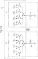
- Figure 1A is a schematic circuit diagram of a four-phase (i.e. multiphase) current-mode (current-steering) sampler 42 corresponding closely to Figure 10 in EP-A1-2211468 , and is merely one example of circuitry which is configured to operate based on a differential current signal.
- four-phase (i.e. multiphase) current-mode (current-steering) sampler 42 corresponding closely to Figure 10 in EP-A1-2211468 , and is merely one example of circuitry which is configured to operate based on a differential current signal.
- the current-mode sampler 42 is configured to sample a differential input signal, current I IN , as shown, by dividing the component current signals (at tail nodes 60 and 66 as described later) into a series of current pulses (samples) which can then be converted into representative digital values to perform an overall analogue-to-digital conversion function.
- current I IN differential input signal
- the sampler 42 is configured to receive the differential input current signal, modeled here as a current source I IN , by way of the currents at tail nodes 60 and 66 whose magnitudes vary with I IN . Because of the differential signaling, sampler 42 effectively has two matching (or corresponding or complementary) sections 54 and 56 for the two differential inputs, shown here also including circuitry which provides the currents at tail nodes 60 and 66 based on I IN to help in an understanding.
- n-channel MOSFETs 58 A to 58 D i.e. one per stream or path
- source terminals connected together at a common tail node 60.
- the aforementioned current source I IN is connected between the common tail node 60 and an equivalent common tail node 66 of section 56.
- a further current source I DC 62 is connected between the common tail node 60 and ground supply, and carries a constant DC current I DC .
- These current sources could be considered external to the sampler 42 as indicated in Figure 1A , and used to provide the currents at tail nodes 60 and 66.
- the gate terminals of the four transistors 58 A to 58 D are driven by the four clock signals ⁇ 0 to ⁇ 3 , respectively, provided e.g. from a VCO (Voltage-Controlled Oscillator).
- section 56 is structurally similar to section 54 and thus comprises transistors 64 A to 64 D , the common tail node 66 and current source I DC 68.
- Figure 2 shows schematic waveforms for the clock signals ⁇ 0 to ⁇ 3 in the upper graph, and schematic waveforms for the corresponding output currents IOUT A to IOUT D in the lower graph.
- the clock signals ⁇ 0 to ⁇ 3 are time-interleaved raised cosine waveforms provided as four voltage waveforms from the VCO.
- the use of four clock signals in the present case is due to the four-way-interleaving design of ADC circuitry 40, but it will be appreciated that, in another arrangement, two or more time-interleaved clock signals could be used, for a two-or-more-way split of the input current signal.
- Clock signals ⁇ 0 to ⁇ 3 are 90° out of phase with one another, such that ⁇ 0 is at 0° phase, ⁇ 1 is at 90° phase, ⁇ 2 is at 180° phase, and ⁇ 3 is at 270° phase.
- sampling circuitry 42 under control of clock signals ⁇ 0 to ⁇ 3 , is that the output currents IOUT A to IOUT D are four trains (or streams) of current pulses, the series of pulses in each train having the same period as one of the clock signals ⁇ 0 to ⁇ 3 , and the pulses of all four trains together being time-interleaved with one another as an effective overall train of pulses at a quarter of the period of one of the clock signals (or at four times the sampling frequency of one of the clock signals).
- the sampler thus operates in the current domain, i.e. effectively as the sampling stage of a current-mode ADC.
- the input signal required is a current signal.
- typical signals that require use of an ADC or sampler are voltage-domain signals, in which the variable under examination is a voltage rather than a current.
- Figure 3 is a schematic circuit diagram of an example implementation 102 of sampling circuitry (sampler) 42, with additional differential voltage-to-current conversion circuitry to which it is possible to apply an input differential voltage signal so as to arrive at the currents at tail nodes 60 and 66.
- Implementation 102 similarly to circuitry 42, comprises two sections 54 and 56 for the so-called “plus” and “minus” components of the differential signals.
- Section 54 comprises switching transistors 58 A to 58 D connected to common tail node 60
- section 56 comprises switching transistors 64 A to 64 D connected to common tail node 66, as before.
- Implementation 102 basically works by receiving the input voltage signal and by employing resistances to passively convert the received input voltage signal into an equivalent input current signal.
- Implementation 102 therefore comprises input terminals 104 (VINP) and 106 (VINM) to receive the "plus” and “minus” components of the input voltage signal, respectively.
- Input terminals 104 and 106 are each connected to a shared terminal 108 via a resistor 110 and an inductor 112. Input terminals 104 and 106 are further each connected to their corresponding common tail nodes 60 and 66 via a resistor 114.
- Shared terminal 108 is connected via shared DC current source 116 to a reference potential whose voltage level is below that of VINP and VINM, and may indeed be negative.
- FIG. 3 An example set of resistance values are shown in Figure 3 . These values have been chosen assuming an example design objective that the input impedance looking into each of the common tail nodes 60 and 66 towards the switching transistors (sampler switches) is 50 ⁇ , and that the input impedance looking into each of the input terminals 104 and 106 is also 50 ⁇ as shown in Figure 3 .
- differential voltage-to-current conversion circuitry comprising: a power supply node for connection to a power supply voltage source; a first current path extending from the power supply node via a first intermediate node to a first load node to provide a first load current at the first load node for use by load circuitry when connected to the first load node, wherein a first supply-connection impedance is connected along the first current path between the power supply node and the first intermediate node and a first load-connection impedance is connected along the first current path between the first intermediate node and the first load node; a second current path extending, in parallel with the first current path, from the power supply node via a second intermediate node to a second load node to provide a second load current at the second load node for use by the load circuitry when connected to the second load node, wherein a second supply-connection impedance is connected along the second current path between the power supply node and the second intermediate no
- Such circuitry exhibits highly linear voltage-to-current conversion, highly efficient signal power conversion by means of highly-controlled input impedance, direct signal current feedthrough from the first and second current paths to subsequent load circuitry, and adjustable gain of the swing of the differential input voltage signal to the swing of the differential current signal.
- the control circuitry may be configured to control the bias voltage provided to the gate or base terminals of the first and second transistors based on a common-mode voltage indicative of a common mode between the source or emitter voltages of the first and second transistors.
- the control circuitry may comprise first and second measurement impedances connected in series between the source or emitter terminals of the first and second transistors, and may be configured to obtain the common-mode voltage from a node between the first and second measurement impedances.
- the first and second measurement impedances may be implemented as resistors.
- the first and second measurement impedances may have the same impedance (e.g. resistance) as one another.
- the control circuitry may be configured to control the bias voltage provided to the gate or base terminals of the first and second transistors based on a difference between the common-mode voltage and a target voltage.
- the control circuitry may be configured to control the bias voltage provided to the gate or base terminals of the first and second transistors such that the first and second load-connection impedances associated with the first and second transistors, respectively, are lower in impedance than the impedances of the first and second supply-connection impedances, respectively.
- the differential voltage-to-current conversion circuitry may comprise a first current sink connected to the first load node so as to draw a first sink current from the first load node, and a second current sink connected to the second load node so as to draw a second sink current from the second load node.
- the first and second load currents may comprise respective component currents of the differential current signal superimposed on a load bias current.
- the first and second current sinks may be controllable current sinks.
- the control circuitry may be configured to control the load bias currents by controlling the first and second sink currents.
- the control circuitry may be configured to control the first and second sink currents so as to regulate the load bias currents at a target bias current value, or so as to compensate for changes in the drain or collector currents of the first and second transistors due to changes in the bias voltages provided to the gate or base terminals of the first and second transistors.
- the control circuitry may be configured to adjust the target bias current value based on a control input signal.
- the first and second supply-connection impedances may be implemented as resistors.
- the first and second supply-connection impedances may have the same impedance (e.g. resistance) as one another.
- the first and second input-connection impedances may be implemented as resistors.
- the first and second input-connection impedances may have the same impedance (e.g. resistance) as one another.
- analogue-to-digital conversion circuitry operable to generate a digital output signal based upon an analogue input differential current signal
- the analogue-to-digital conversion circuitry comprises differential voltage-to-current conversion circuitry according to the aforementioned first aspect of the present invention
- the differential voltage-to-current conversion circuitry is configured to generate the input differential current signal as said differential current signal dependent on the differential input voltage signal.
- integrated circuitry such as an IC chip, comprising differential voltage-to-current conversion circuitry according to the aforementioned first aspect of the present invention, or analogue-to-digital conversion circuitry according to the aforementioned second aspect of the present invention.
- the present invention extends to method or computer program aspects (e.g. for control) corresponding to the apparatus (circuitry) aspects.
- Figure 4 is a schematic diagram of differential voltage-to-current conversion circuitry 200 shown receiving a differential input voltage signal and outputting a corresponding differential current signal to load circuitry 300.
- the conversion circuitry 200 is shown effectively drawing the current from a power supply voltage source VDDH (VDD High) with that current being sinked to a ground (GND) power supply voltage source via the load circuitry 300 (which has its own supply voltage source VDDL or VDD Low, where VDDH>VDDL).
- VDD power supply voltage source
- VDD Low ground
- VDDL ground
- VDDH voltage source
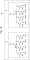
- sampler 42a sinks currents at the corresponding tail nodes 60a and 66a from the conversion circuitry 200 and passes them through the corresponding switching transistors 58a and 64a towards ground (GND) (being the case which aligns with that depicted in Figure 4 ).
- the sampler 42a receive currents at the tail nodes 60a and 66a from the Figure 4 conversion circuitry 200 (nodes 206 and 210) and passes them through the switching transistors 58a and 64a towards the ADC's sampling capacitors (not shown) effectively serving as a virtual GND.
- sampler 42a - and ADC circuitry comprising the sampler 42a - may serve as the load circuitry 300.
- the conversion circuitry 200 may be considered front-end circuitry for the sampler 42a and ADC circuitry comprising the sampler 42a. The present disclosure will be understood accordingly.
- the conversion circuitry 200 comprises a first (e.g. "plus") current path extending from a power supply voltage node 202 at VDDH (VDD High) via a first intermediate node 204 to a first load node 206 to provide a first load current I L1 at the first load node 206 for use by the load circuitry 300 when it is connected to the first load node 206 as in Figure 4 .
- the conversion circuitry 200 also comprises a second (e.g.
- the first and second load currents I L1 and I L2 may thus be considered as “plus” and “minus” component currents of a differential current signal provided by the conversion circuitry 200 to the load circuitry 300.
- a first supply-connection impedance 212 is connected along the first current path between the power supply node 202 and the first intermediate node 204, and a first load-connection impedance 214 is connected along the first current path between the first intermediate node 204 and the first load node 206.
- a second supply-connection impedance 216 is connected along the second current path between the power supply node 202 and the second intermediate node 208, and a second load-connection impedance 218 is connected along the second current path between the second intermediate node 208 and the second load node 210.
- the first and second supply-connection impedances 212 and 216 are implemented as resistors having resistances R B1 and R B2 , respectively.
- the first and second-connection impedances 214 and 218 are both implemented as transistors, in this case as PMOS MOSFETs M1 and M2, respectively, in a common gate configuration so that they present input impedances Z G1 and Z G2 , respectively, which can be controlled by gate bias voltages V BIAS1 and V BIAS2 , respectively.
- Optional smoothing capacitors are shown at their gate terminals.
- the bias voltages are bias voltages in the sense that they are stable or effectively DC voltages, independent of the differential input voltage signal Vindiff.
- a differential voltage input 220 is connected between the first and second intermediate nodes 204 and 208 via first and second input-connection impedances 222 and 224, respectively, for application of a differential input voltage signal Vindiff, supplied at the differential voltage input 220, between the first and second input-connection impedances 222 and 224 as shown in Figure 4 .
- the first and second load currents I L1 and I L2 which define the differential current signal, are dependent on the differential input voltage signal Vindiff.
- the first and second input-connection impedances 222 and 224 are implemented as resistors having resistances R O1 and R O2 , respectively.
- bias currents I B1 and I B2 flow through resistors 212 and 216, respectively, that current Is flows from intermediate node 208 to intermediate node 204 dependent on the differential input voltage signal Vindiff, that signal currents I SIG1 and I SIG2 flow through transistors 214 and 218, respectively, and that currents I L1 and I L2 are provided at load nodes 206 and 210, respectively.
- the bias currents are bias currents in that they are stable or DC currents, independent of the differential input voltage signal Vindiff.
- sink currents I SK1 and I SK2 (to be described later) are drawn from the drain terminals of the transistors 214 and 218, respectively.
- Control circuitry 230 is provided to control the bias voltages V BIAS1 and V BIAS2 , since this has the effect of controlling the gain relationship between the differential input voltage signal Vindiff and the differential current signal.
- controlling the bias voltages V BIAS1 and V BIAS2 controls the impedance values Z G1 and Z G2 , respectively.
- Figure 5 presents an equivalent circuit diagram 200-E of the conversion circuitry 200 of Figure 4 .
- the front-end circuitry exhibits highly linear voltage-to-current conversion, highly efficient signal power conversion by means of highly-controlled input impedance, direct signal current feedthrough from the first and second current paths to the subsequent load circuitry (e.g. through the switching transistors 58 and 64 of the sampler 42), and adjustable gain of the swing of the differential input voltage signal Vindiff to the swing of the differential current signal.
- Vindiff is the differential input voltage signal applied to the circuit via input-connection resistors 222 and 224 to the first current path ("plus” or P-branch) and the second current path ("minus” or N-branch) as in Figure 4 .
- the active stage input impedance Z G i.e. associated with the transistors 214 and 218, is dimensioned to be much smaller than the bias resistance R B through which the effective bias current 'i S ' flows.
- Varying impedance Z G then leads to slight adjustments of the gain of the transfer function.
- the transistors 214 and 218 form a common gate stage.
- This stage is biased and dimensioned in a way to have a very low input impedance (i.e. Z G ⁇ R B ) and a very high output impedance providing the subsequent load circuitry 300 with a bias current on which is superimposed a differential signal current (the two together constituting the current components - i.e. the load currents - of the overall differential current signal).
- This current is highly proportional to the differential input voltage signal Vindiff. Therefore the subsequent load circuitry 300 can be treated low-ohmic and it does not affect the signal power-to-current conversion.
- the impedance Z G ⁇ 1/gm proportional to ⁇ 1/ ⁇ I D , where I D is the drain current and gm is the transconductance of the transistors.
- the impedance Z G can be controlled by controlling the common mode value of the drain current I D (effectively by controlling the bias current I B ), i.e. by controlling the gate-source voltages of the transistors 214 and 218 by controlling the bias voltages V BIAS1 and V BIAS2 as mentioned above.
- the difference between the bias current I B and the sink current I SK (being L) is regulated (e.g. unaffected by changes in the bias current I B ).
- This regulation can be done in an automatic control loop, as considered later in connection with Figures 6B and 7 .
- the control may also be such that the value of the difference between the bias current I B and the sink current I SK can be varied to vary the amount of current supplied to the load circuitry 300, for example to optimize the operation of the load circuitry 300. This will also be considered later in connection with Figures 6B and 7 .
- control circuitry 230 is configured to receive a control signal CONTROL, and based on that signal to generate the control signals V BIAS1 , V BIAS2 , SINK1 and SINK2.
- the control circuitry 230 is also configured to receive a common-mode voltage V CM being representative of the common-mode value of the source voltages of the transistors 214 and 218.
- Measurement impedances 240 and 242 are connected in series between the source terminals 244 and 246 of the transistors 214 and 218, respectively, and the V CM signal is taken from a node 248 between the measurement impedances 240 and 242.
- a part 230-A of the control circuitry 230 is shown, comprising a current DAC (Digital-to-Analogue Converter) or IDAC 402, a resistor 404 and a differential amplifier 406 (e.g. an operational amplifier).
- DAC Digital-to-Analogue Converter
- IDAC analog-to-Analogue Converter
- resistor 404 e.g. an operational amplifier
- the IDAC 402 is connected in series with the resistor 404 between VDD (e.g. VDDH) and GND to form a potential divider arrangement.
- the IDAC 402 is controlled by part of the (digital) control signal CONTROL to cause a current I PD1 to flow through the resistor 404 such that a desired reference voltage Vref1 is produced at a node 408 along the potential divider between the IDAC 402 and the resistor 404.
- the differential amplifier 406 is connected to receive the reference voltage Vref1 and the common-mode voltage V CM at its input terminals, and to output the common gate bias V BIAS based upon a difference between the reference voltage Vref1 and the common-mode voltage V CM .
- the differential amplifier 406 controls or regulates the common gate bias V BIAS such that it tends towards the reference voltage Vref1, at which the difference between the reference voltage Vref1 and the common-mode voltage V CM is minimized. This has the effect of regulating the bias current I B .
- the control signal CONTROL can thus be adjusted to adjust the reference voltage Vref1 and therefore the bias current I B . This enables digital (programmable) control of the bias current I B .
- the control may be such that the value of the difference between the bias current I B and the sink current I SK can be varied to vary the amount of current supplied to the load circuitry 300, for example to optimize the operation of the load circuitry 300.
- a part 230-B of the control circuitry 230 is shown, comprising an IDAC 502, a resistor 504 and a logic unit 506 (which may be implemented as a processor executing a computer program).
- the IDAC 402 is connected in series with the resistor 404 between VDD (e.g. VDDH) and GND to form a potential divider arrangement.
- the IDAC 502 is controlled by part of the (digital) control signal CONTROL to cause a current I PD2 to flow through the resistor 404 such that a desired reference voltage Vref2 is produced at a node 508 along the potential divider between the IDAC 502 and the resistor 504.
- the logic unit 506 is connected to receive the reference voltage Vref2, the common-mode voltage V CM and the common gate bias V BIAS (generated by part 230-A of the control circuitry 230) at its input terminals, and to output the control signal SINK based on those input signals.
- the common-mode voltage V CM and the common gate bias V BIAS together give a measure of the common-mode gate-source voltage V GS of the transistors 214 and 218, as indicated in Figure 6B .
- the common gate bias V BIAS itself may also be considered a measure of the common-mode gate-source voltage V GS of the transistors 214 and 218 in which case the common-mode voltage V CM need not be supplied to the logic unit 506.
- the measure of the common-mode gate-source voltage V GS of the transistors 214 and 218 is taken as a measure of the bias current I B (i.e. the common mode drain current I D ).
- the reference voltage Vref2 is taken as a measure of a target bias current I T (i.e. a target common mode drain current I D ).
- the logic unit 506 then adjusts the control signal SINK so that the bias current I B tends towards or is regulated at the target bias current I T .
- the control signal CONTROL can thus be adjusted to adjust the reference voltage Vref2 and therefore the target bias current I T .
- This enables digital (programmable) control of the target bias current I T , and thus of the difference between the bias current I B and the sink current I SK .
- the control signal CONTROL is maintained the same in respect of the target bias current I T , then the difference between the bias current I B and the sink current I SK is regulated to that value.
- the control may be such that the value of the difference between the bias current I B and the sink current I SK can be varied to vary the amount of current supplied to the load circuitry 300.
- bias current I B here is defined as that following through the transistors 214 and 218 (i.e. prior to the drawing of current I SK by the current sinks 232 and 234)
- I BL I B - I SK
- the control based on Vref2 serves to control the sum of the load bias current I BL and the sink current I SK .
- Figure 7 is a flow diagram of an example method 600 useful for understanding the operation of the logic unit 506 and in addition takes into account a possible logic operation which is more sophisticated than the corresponding operation of the differential amplifier 406 (it will be appreciated that the amplifier 406 could be replaced with a logic unit operating in accordance with the relevant steps of method 600).
- Method 600 has steps S2 to S20.
- method 600 is a two-step DC regulation scheme, comprising overall Steps 1 and 2 as indicated.
- Step 1 (corresponding to the operation in Figure 6A ) is for optimization of the input impedance Z G by adjustment of bias current I B (by adjusting the V BIAS gate signals) through control of target value I BT .
- Step 2 (corresponding to the operation in Figure 6B ) if for optimization of the DC load current I L (which is I L1 ,I L2 in Figure 4 and shown as I LOAD in Figure 7 ) with respect to a maximum voltage range V CapDC on a sampling capacitor C Load by adjustment of sink current I SK to a target value of the load current I LoadT .
- sampling capacitor C Load may be consider to be at the end of each of the paths shown in Figure 1B (e.g. to be charged up by the current IOUT A within the sampling frequency fSampling to values V CapDC - see below).
- step S2 a value of the target bias current I BT is set based on the reference voltage Vref1 (see Figure 6A ) to optimize input impedance Z G .
- the method then proceeds to step S4 in which the target sink current I SKT is set based on Vref2 (see Figure 6B ) to optimize operating range on sampling capacitor C LOAD .
- step S6 the existing bias current I B is measured based on V GS .
- the common-mode voltage V CM and the common gate bias V BIAS together give a measure of the common-mode gate-source voltage V GS of the transistors 214 and 218, as indicated in Figure 6B .
- the method then proceeds to step S8.
- step S8 it is determined whether the existing bias current I B is greater than the target bias current I BT . If it is (step S8, I B >I BT ), the method proceeds to step S14. Otherwise (step S8, I B ⁇ I BT ), the method proceeds to step S16.
- step S14 the V BIAS1,2 signals are controlled to both decrease the bias current I B to or towards the target value I BT .
- step S16 the V BIAS1,2 signals are controlled to both increase the bias current I B to or towards the target value I BT .
- step S10 If the measured value I B equals the target value I BT the method proceeds with step S10.
- the correct value of I B is desirable to optimize the input impedance of Z G1 , Z G2 .
- step S10 the existing load current I LOAD (I L ) feeding load capacitors in the subsequent load circuitry 300 (ADC stage) is measured. The method then proceeds to step S12.
- step S12 it is determined whether the existing load current I LOAD is greater than the target load current I LoadT . If it is (step S12, I LOAD >I LoadT ), the method proceeds to step S18. Otherwise (step S12, I LOAD ⁇ I LoadT ), the method proceeds to step S20.
- step S18 the SINK signals are controlled to increase the sink currents I SK to bring the load currents I LOAD to or towards the target value I LoadT .
- step S20 the SINK signals are controlled to decrease the sink currents I SK to bring the load currents I LOAD to or towards the target value I LoadT . If the measured value I LOAD equals the target value I LoadT the method ends.
- the correct value of I LOAD is desirable to optimize the operating voltage range on the sampling capacitor C LOAD .
- the method 600 then continues until operation is stopped - for example if it is determined that the V BIAS and SINK signals have optimal values which need not be changed for the time being.
- the method 600 may be run from time to time.
- the logic unit 506 (along with a corresponding unit replacing amplifier 406) may be implemented in software running on a processor or in analogue circuitry.
- Figure 8 is a schematic diagram of a circuitry system 700, comprising the conversion (or front-end) circuitry 200 and the load circuitry 300 coupled together as in Figure 4 .
- the conversion circuitry 200 receives a differential input voltage signal Vindiff and outputs a corresponding differential current signal as the input differential current signal lindiff for the load circuitry 300.
- the load circuitry 300 may be ADC circuitry configured based on the sampler 42a (see Figure 1B ) and explained in more detail in EP-A1-2211468 to generate a digital output signal as shown in Figure 8 based on the input differential current signal lindiff.
- the circuitry system 700 could be referred to as ADC circuitry.
- the conversion (or front-end) circuitry 200 and the load circuitry 300 could both be implemented as integrated circuitry, provided for example on an IC chip.
- the circuitry system 700 could be referred to as integrated circuitry, and may be provided on or as a single IC chip.
- MOSFET or FET transistors 214 and 218 could instead be BJTs, and the present disclosure will be understood accordingly.
- Circuitry of the present invention may be implemented as integrated circuitry, for example on an IC chip such as a flip chip.
- the present invention extends to integrated circuitry and IC chips as mentioned above, circuit boards comprising such IC chips, and communication networks (for example, internet fiber-optic networks and wireless networks) and network equipment of such networks, comprising such circuit boards.
- the various features may be implemented in hardware, or as software modules running on one or more processors. Features of one aspect may be applied to any of the other aspects.
- the invention also provides a computer program or a computer program product for carrying out any of the methods described herein, and a computer readable medium having stored thereon a program for carrying out any of the methods described herein.
- a computer program embodying the invention may be stored on a computer-readable medium, or it could, for example, be in the form of a signal such as a downloadable data signal provided from an Internet website, or it could be in any other form.
Landscapes
- Engineering & Computer Science (AREA)
- Power Engineering (AREA)
- Computer Hardware Design (AREA)
- Physics & Mathematics (AREA)
- Theoretical Computer Science (AREA)
- Mathematical Physics (AREA)
- General Engineering & Computer Science (AREA)
- Computing Systems (AREA)
- Electromagnetism (AREA)
- General Physics & Mathematics (AREA)
- Radar, Positioning & Navigation (AREA)
- Automation & Control Theory (AREA)
- Amplifiers (AREA)
Abstract
Description
- The present invention relates to circuitry for voltage-to-current conversion, and in particular to differential voltage-to-current conversion circuitry. Such circuitry is operable to receive a differential voltage input signal and output a corresponding differential current signal.
- To understand the potential use of differential voltage-to-current conversion circuitry,
Figure 1A is a schematic circuit diagram of a four-phase (i.e. multiphase) current-mode (current-steering) sampler 42 corresponding closely to Figure 10 inEP-A1-2211468 , and is merely one example of circuitry which is configured to operate based on a differential current signal. - The current-mode sampler 42 is configured to sample a differential input signal, current IIN, as shown, by dividing the component current signals (at
tail nodes EP-A1-2211468 . - The sampler 42 is configured to receive the differential input current signal, modeled here as a current source IIN, by way of the currents at
tail nodes sections tail nodes section 54 and a second set of matching output streams IOUTBA to IOUTBD, where IOUTB meansIOUT , and wherein IOUTA is paired with IOUTBA, IOUTB is paired with IOUTBB, and so on and so forth. - Focusing on the
first section 54 by way of example (because thesecond section 56 operates analogously to the first section 54), there are provided four n-channel MOSFETs 58A to 58D (i.e. one per stream or path) with their source terminals connected together at acommon tail node 60. - The aforementioned current source IIN is connected between the
common tail node 60 and an equivalentcommon tail node 66 ofsection 56. A further current source IDC 62 is connected between thecommon tail node 60 and ground supply, and carries a constant DC current IDC. These current sources could be considered external to the sampler 42 as indicated inFigure 1A , and used to provide the currents attail nodes - As mentioned above,
section 56 is structurally similar tosection 54 and thus comprises transistors 64A to 64D, thecommon tail node 66 and current source IDC 68. -
Figure 2 shows schematic waveforms for the clock signals θ0 to θ3 in the upper graph, and schematic waveforms for the corresponding output currents IOUTA to IOUTD in the lower graph. - The clock signals θ0 to θ3 are time-interleaved raised cosine waveforms provided as four voltage waveforms from the VCO. The use of four clock signals in the present case is due to the four-way-interleaving design of ADC circuitry 40, but it will be appreciated that, in another arrangement, two or more time-interleaved clock signals could be used, for a two-or-more-way split of the input current signal.
- Clock signals θ0 to θ3 are 90° out of phase with one another, such that θ0 is at 0° phase, θ1 is at 90° phase, θ2 is at 180° phase, and θ3 is at 270° phase.
- The effect of sampling circuitry 42, under control of clock signals θ0 to θ3, is that the output currents IOUTA to IOUTD are four trains (or streams) of current pulses, the series of pulses in each train having the same period as one of the clock signals θ0 to θ3, and the pulses of all four trains together being time-interleaved with one another as an effective overall train of pulses at a quarter of the period of one of the clock signals (or at four times the sampling frequency of one of the clock signals).
- The sampler thus operates in the current domain, i.e. effectively as the sampling stage of a current-mode ADC. For further detail, reference may be made again to
EP-A1-2211468 . As a result, the input signal required is a current signal. However, typical signals that require use of an ADC or sampler are voltage-domain signals, in which the variable under examination is a voltage rather than a current. -
Figure 3 is a schematic circuit diagram of anexample implementation 102 of sampling circuitry (sampler) 42, with additional differential voltage-to-current conversion circuitry to which it is possible to apply an input differential voltage signal so as to arrive at the currents attail nodes -
Implementation 102, similarly to circuitry 42, comprises twosections Section 54 comprises switching transistors 58A to 58D connected tocommon tail node 60, andsection 56 comprises switching transistors 64A to 64D connected tocommon tail node 66, as before. -
Implementation 102 basically works by receiving the input voltage signal and by employing resistances to passively convert the received input voltage signal into an equivalent input current signal.Implementation 102 therefore comprises input terminals 104 (VINP) and 106 (VINM) to receive the "plus" and "minus" components of the input voltage signal, respectively. -
Input terminals terminal 108 via aresistor 110 and aninductor 112.Input terminals common tail nodes resistor 114.Shared terminal 108 is connected via shared DCcurrent source 116 to a reference potential whose voltage level is below that of VINP and VINM, and may indeed be negative. - An example set of resistance values are shown in
Figure 3 . These values have been chosen assuming an example design objective that the input impedance looking into each of thecommon tail nodes input terminals Figure 3 . - Unfortunately, there are disadvantages associated with the example circuitry used for voltage-to-current conversion shown in
Figure 3 . The voltage-to-current conversion is considered relatively inefficient in some applications which limits the resolution of overall ADC circuitry employing the sampler 42. Further, the gain associated with the conversion may not be optimal in some applications. - It is desirable to solve some or all of the above problems.
- According to an embodiment of a first aspect of the present invention, there is provided differential voltage-to-current conversion circuitry, comprising: a power supply node for connection to a power supply voltage source; a first current path extending from the power supply node via a first intermediate node to a first load node to provide a first load current at the first load node for use by load circuitry when connected to the first load node, wherein a first supply-connection impedance is connected along the first current path between the power supply node and the first intermediate node and a first load-connection impedance is connected along the first current path between the first intermediate node and the first load node; a second current path extending, in parallel with the first current path, from the power supply node via a second intermediate node to a second load node to provide a second load current at the second load node for use by the load circuitry when connected to the second load node, wherein a second supply-connection impedance is connected along the second current path between the power supply node and the second intermediate node and a second load-connection impedance is connected along the second current path between the second intermediate node and the second load node; a differential voltage input connected between the first and second intermediate nodes via first and second input-connection impedances, respectively, for application of a differential input voltage signal, supplied at the differential voltage input, between the first and second input-connection impedances so that the first and second load currents together define a differential current signal dependent on the differential input voltage signal; and control circuitry, wherein: the first and second load-connection impedances are implemented as first and second transistors, respectively; and the control circuitry is configured to control a bias voltage provided to the gate or base terminals of the first and second transistors so as to control a gain relationship between the differential input voltage signal and the differential current signal.
- Such circuitry exhibits highly linear voltage-to-current conversion, highly efficient signal power conversion by means of highly-controlled input impedance, direct signal current feedthrough from the first and second current paths to subsequent load circuitry, and adjustable gain of the swing of the differential input voltage signal to the swing of the differential current signal.
- The control circuitry may be configured to control the bias voltage provided to the gate or base terminals of the first and second transistors based on a common-mode voltage indicative of a common mode between the source or emitter voltages of the first and second transistors.
- The control circuitry may comprise first and second measurement impedances connected in series between the source or emitter terminals of the first and second transistors, and may be configured to obtain the common-mode voltage from a node between the first and second measurement impedances.
- The first and second measurement impedances may be implemented as resistors. The first and second measurement impedances may have the same impedance (e.g. resistance) as one another.
- The control circuitry may be configured to control the bias voltage provided to the gate or base terminals of the first and second transistors based on a difference between the common-mode voltage and a target voltage.
- The control circuitry may be configured to control the bias voltage provided to the gate or base terminals of the first and second transistors such that the first and second load-connection impedances associated with the first and second transistors, respectively, are lower in impedance than the impedances of the first and second supply-connection impedances, respectively.
- The differential voltage-to-current conversion circuitry may comprise a first current sink connected to the first load node so as to draw a first sink current from the first load node, and a second current sink connected to the second load node so as to draw a second sink current from the second load node.
- The first and second load currents may comprise respective component currents of the differential current signal superimposed on a load bias current. The first and second current sinks may be controllable current sinks. The control circuitry may be configured to control the load bias currents by controlling the first and second sink currents.
- The control circuitry may be configured to control the first and second sink currents so as to regulate the load bias currents at a target bias current value, or so as to compensate for changes in the drain or collector currents of the first and second transistors due to changes in the bias voltages provided to the gate or base terminals of the first and second transistors.
- The control circuitry may be configured to adjust the target bias current value based on a control input signal.
- The first and second supply-connection impedances may be implemented as resistors. The first and second supply-connection impedances may have the same impedance (e.g. resistance) as one another. The first and second input-connection impedances may be implemented as resistors. The first and second input-connection impedances may have the same impedance (e.g. resistance) as one another.
- According to an embodiment of a second aspect of the present invention, there is provided analogue-to-digital conversion circuitry operable to generate a digital output signal based upon an analogue input differential current signal, wherein: the analogue-to-digital conversion circuitry comprises differential voltage-to-current conversion circuitry according to the aforementioned first aspect of the present invention; and the differential voltage-to-current conversion circuitry is configured to generate the input differential current signal as said differential current signal dependent on the differential input voltage signal.
- According to an embodiment of a third aspect of the present invention, there is provided integrated circuitry, such as an IC chip, comprising differential voltage-to-current conversion circuitry according to the aforementioned first aspect of the present invention, or analogue-to-digital conversion circuitry according to the aforementioned second aspect of the present invention.
- The present invention extends to method or computer program aspects (e.g. for control) corresponding to the apparatus (circuitry) aspects.
- Reference will now be made, by way of example only, to the accompanying Figures, of which:
-
Figure 1A , considered above, is a schematic circuit diagram of a multiphase current-mode sampler; -
Figure 1B , is a schematic circuit diagram of a multiphase current-mode sampler corresponding toFigure 1A but using PMOS transistors; -
Figure 2 , considered above, shows schematic waveforms useful for understanding the sampler ofFigure 1A ; -
Figure 3 , considered above, is a schematic circuit diagram of an example implementation of theFigure 1A sampler; -
Figure 4 is a schematic diagram of differential voltage-to-current conversion circuitry embodying the present invention; -
Figure 5 is an equivalent circuit diagram of the conversion circuitry ofFigure 4 ; -
Figure 6A is a schematic diagram useful for understanding one way of regulating the bias current inFigure 4 ; -
Figure 6B is a schematic diagram useful for understanding one way of biasing the current sinks inFigure 4 ; -
Figure 7 is a flow diagram of an example method useful for understanding the operation of the logic unit ofFigure 6B ; and -
Figure 8 is a schematic diagram of a circuitry system comprising theFigure 4 circuitry. -
Figure 4 is a schematic diagram of differential voltage-to-current conversion circuitry 200 shown receiving a differential input voltage signal and outputting a corresponding differential current signal to loadcircuitry 300. - The
conversion circuitry 200 is shown effectively drawing the current from a power supply voltage source VDDH (VDD High) with that current being sinked to a ground (GND) power supply voltage source via the load circuitry 300 (which has its own supply voltage source VDDL or VDD Low, where VDDH>VDDL). However, the reverse situation is also possible, with the current effectively flowing down from VDD (e.g. VDDH) through theload circuitry 300 and then through theconversion circuitry 200. - This latter case may indeed seem more appropriate given the direction of current flow through the
tail nodes Figure 1A . - However, equally, the sampler 42 general configuration could be provided effectively the other way up as shown in
Figure 1B by way ofsampler 42a which corresponds to sampler 42.Sampler 42a sinks currents at thecorresponding tail nodes conversion circuitry 200 and passes them through the corresponding switching transistors 58a and 64a towards ground (GND) (being the case which aligns with that depicted inFigure 4 ). Thesampler 42a receive currents at thetail nodes Figure 4 conversion circuitry 200 (nodes 206 and 210) and passes them through the switching transistors 58a and 64a towards the ADC's sampling capacitors (not shown) effectively serving as a virtual GND. - It will thus be understood that the
sampler 42a - and ADC circuitry comprising thesampler 42a - may serve as theload circuitry 300. As such, theconversion circuitry 200 may be considered front-end circuitry for thesampler 42a and ADC circuitry comprising thesampler 42a. The present disclosure will be understood accordingly. - The
conversion circuitry 200 comprises a first (e.g. "plus") current path extending from a powersupply voltage node 202 at VDDH (VDD High) via a firstintermediate node 204 to afirst load node 206 to provide a first load current IL1 at thefirst load node 206 for use by theload circuitry 300 when it is connected to thefirst load node 206 as inFigure 4 . Theconversion circuitry 200 also comprises a second (e.g. "minus") current path extending, in parallel with the first current path, from the powersupply voltage node 202 via a secondintermediate node 208 to asecond load node 210 to provide a second load current IL2 at thesecond load node 210 for use by theload circuitry 300, again when it is connected to thesecond load node 210 as inFigure 4 . - The first and second load currents IL1 and IL2 may thus be considered as "plus" and "minus" component currents of a differential current signal provided by the
conversion circuitry 200 to theload circuitry 300. - A first supply-
connection impedance 212 is connected along the first current path between thepower supply node 202 and the firstintermediate node 204, and a first load-connection impedance 214 is connected along the first current path between the firstintermediate node 204 and thefirst load node 206. Similarly, a second supply-connection impedance 216 is connected along the second current path between thepower supply node 202 and the secondintermediate node 208, and a second load-connection impedance 218 is connected along the second current path between the secondintermediate node 208 and thesecond load node 210. - The first and second supply-
connection impedances connection impedances transistors - A
differential voltage input 220 is connected between the first and secondintermediate nodes connection impedances differential voltage input 220, between the first and second input-connection impedances Figure 4 . Thus, the first and second load currents IL1 and IL2, which define the differential current signal, are dependent on the differential input voltage signal Vindiff. The first and second input-connection impedances - Looking at
Figure 4 , it is assumed that bias currents IB1 and IB2 flow throughresistors intermediate node 208 tointermediate node 204 dependent on the differential input voltage signal Vindiff, that signal currents ISIG1 and ISIG2 flow throughtransistors load nodes transistors -
Control circuitry 230 is provided to control the bias voltages VBIAS1 and VBIAS2, since this has the effect of controlling the gain relationship between the differential input voltage signal Vindiff and the differential current signal. In this regard, controlling the bias voltages VBIAS1 and VBIAS2 controls the impedance values ZG1 and ZG2, respectively. The significance of this can be better appreciated through consideration ofFigure 5 , which presents an equivalent circuit diagram 200-E of theconversion circuitry 200 ofFigure 4 . - In
Figure 5 , like components are denoted with like reference signs for ease of comparison withFigure 4 , and duplicate description is omitted. For simplicity, and symmetry/balance in the operation, it is assumed inFigures 4 and5 that the first and second current paths are configured in the same way as one another, and in particular that RB1 = RB2 = RB, RO1 = RO2 = RO, and that ZG1 = ZG2 = ZG (in terms of their common-mode value). Thus, it is also assumed that IB1 = IB2 = IB. It is also assumed that ISK1 = ISK2 = ISK. - As an overview, the front-end circuitry (conversion circuitry 200) exhibits highly linear voltage-to-current conversion, highly efficient signal power conversion by means of highly-controlled input impedance, direct signal current feedthrough from the first and second current paths to the subsequent load circuitry (e.g. through the switching transistors 58 and 64 of the sampler 42), and adjustable gain of the swing of the differential input voltage signal Vindiff to the swing of the differential current signal.
- Looking at
Figure 5 , Vindiff is the differential input voltage signal applied to the circuit via input-connection resistors Figure 4 . In order to maximize the effective signal current 'iS', the active stage input impedance ZG (i.e. associated with thetransistors 214 and 218) is dimensioned to be much smaller than the bias resistance RB through which the effective bias current 'iS' flows. Furthermore it is possible to vary the loop current ratio iS/iB and therefore the gain of the transfer function iS=f(Vindiff) can be adjusted. - The transfer function calculates to:

- It can be appreciated that if ZG<<RB, then the transfer function simplifies to:

- Varying impedance ZG then leads to slight adjustments of the gain of the transfer function.
- In order to realize a low impedance ZG in
Figure 4 , thetransistors 214 and 218 (M1, M2) form a common gate stage. This stage is biased and dimensioned in a way to have a very low input impedance (i.e. ZG<<RB) and a very high output impedance providing thesubsequent load circuitry 300 with a bias current on which is superimposed a differential signal current (the two together constituting the current components - i.e. the load currents - of the overall differential current signal). This current is highly proportional to the differential input voltage signal Vindiff. Therefore thesubsequent load circuitry 300 can be treated low-ohmic and it does not affect the signal power-to-current conversion. - The impedance ZG ≈ 1/gm proportional to ≈ 1/√ID, where ID is the drain current and gm is the transconductance of the transistors. Thus, the impedance ZG can be controlled by controlling the common mode value of the drain current ID (effectively by controlling the bias current IB), i.e. by controlling the gate-source voltages of the
transistors Figure 4 ) is regulated by means of common gate bias VBIAS (recall that VBIAS1 = VBIAS2 = VBIAS inFigure 4 ) using bias circuitry containing a voltage regulator and current DAC (as considered later in connection withFigure 6A ). - Furthermore ZG = 1/gm can be adjusted by programmable or other control of the bias current IB (i.e. by adjusting the VBIAS gate signals) while keeping the output signal current unaffected by means of adding programmable/controllable
current sinks Figure 4 ) at the drain terminals of thetransistors Figure 4 . Thecurrent sinks Figures 6B and7 . The control may also be such that the value of the difference between the bias current IB and the sink current ISK can be varied to vary the amount of current supplied to theload circuitry 300, for example to optimize the operation of theload circuitry 300. This will also be considered later in connection withFigures 6B and7 . - Returning to
Figure 4 , thecontrol circuitry 230 is configured to receive a control signal CONTROL, and based on that signal to generate the control signals VBIAS1 , VBIAS2 , SINK1 and SINK2. Thecontrol circuitry 230 is also configured to receive a common-mode voltage VCM being representative of the common-mode value of the source voltages of thetransistors Measurement impedances source terminals transistors node 248 between themeasurement impedances -
Figure 6A is a schematic diagram which, as mentioned above, is useful for understanding one way of regulating the bias current IB (recall that IB1 = IB2 = IB inFigure 4 ) by means of common gate bias VBIAS (recall that VBIAS1 = VBIAS2 = VBIAS inFigure 4 ) using bias circuitry. - For ease of understanding, parts of the
conversion circuitry 200 containing thetransistors conversion circuitry 200 being omitted for simplicity. A part 230-A of thecontrol circuitry 230 is shown, comprising a current DAC (Digital-to-Analogue Converter) orIDAC 402, aresistor 404 and a differential amplifier 406 (e.g. an operational amplifier). - The
IDAC 402 is connected in series with theresistor 404 between VDD (e.g. VDDH) and GND to form a potential divider arrangement. TheIDAC 402 is controlled by part of the (digital) control signal CONTROL to cause a current IPD1 to flow through theresistor 404 such that a desired reference voltage Vref1 is produced at anode 408 along the potential divider between theIDAC 402 and theresistor 404. - The differential amplifier 406 is connected to receive the reference voltage Vref1 and the common-mode voltage VCM at its input terminals, and to output the common gate bias VBIAS based upon a difference between the reference voltage Vref1 and the common-mode voltage VCM. The differential amplifier 406 controls or regulates the common gate bias VBIAS such that it tends towards the reference voltage Vref1, at which the difference between the reference voltage Vref1 and the common-mode voltage VCM is minimized. This has the effect of regulating the bias current IB. The control signal CONTROL can thus be adjusted to adjust the reference voltage Vref1 and therefore the bias current IB. This enables digital (programmable) control of the bias current IB.
-
Figure 6B is a schematic diagram which, as mentioned above, is useful for understanding one way of biasing thecurrent sinks load circuitry 300, for example to optimize the operation of theload circuitry 300. - For ease of understanding, parts of the
conversion circuitry 200 containing thecurrent sinks conversion circuitry 200 being omitted for simplicity. A part 230-B of thecontrol circuitry 230 is shown, comprising anIDAC 502, aresistor 504 and a logic unit 506 (which may be implemented as a processor executing a computer program). - The
IDAC 402 is connected in series with theresistor 404 between VDD (e.g. VDDH) and GND to form a potential divider arrangement. TheIDAC 502 is controlled by part of the (digital) control signal CONTROL to cause a current IPD2 to flow through theresistor 404 such that a desired reference voltage Vref2 is produced at anode 508 along the potential divider between theIDAC 502 and theresistor 504. - The
logic unit 506 is connected to receive the reference voltage Vref2, the common-mode voltage VCM and the common gate bias VBIAS (generated by part 230-A of the control circuitry 230) at its input terminals, and to output the control signal SINK based on those input signals. - The common-mode voltage VCM and the common gate bias VBIAS together give a measure of the common-mode gate-source voltage VGS of the
transistors Figure 6B . The common gate bias VBIAS itself may also be considered a measure of the common-mode gate-source voltage VGS of thetransistors logic unit 506. The measure of the common-mode gate-source voltage VGS of thetransistors logic unit 506 then adjusts the control signal SINK so that the bias current IB tends towards or is regulated at the target bias current IT. - The control signal CONTROL can thus be adjusted to adjust the reference voltage Vref2 and therefore the target bias current IT. This enables digital (programmable) control of the target bias current IT, and thus of the difference between the bias current IB and the sink current ISK. Thus, if the control signal CONTROL is maintained the same in respect of the target bias current IT, then the difference between the bias current IB and the sink current ISK is regulated to that value. By adjusting the control signal CONTROL in respect of the target bias current IT, i.e. adjusting the reference voltage Vref2, the control may be such that the value of the difference between the bias current IB and the sink current ISK can be varied to vary the amount of current supplied to the
load circuitry 300. - Incidentally, although the bias current IB here is defined as that following through the
transistors 214 and 218 (i.e. prior to the drawing of current ISK by thecurrent sinks 232 and 234), there could also be considered to be a load bias current IBL which forms part of the load currents L, where IBL = IB - ISK. Thus, it could be considered that the control based on Vref2 serves to control the sum of the load bias current IBL and the sink current ISK. -
Figure 7 is a flow diagram of anexample method 600 useful for understanding the operation of thelogic unit 506 and in addition takes into account a possible logic operation which is more sophisticated than the corresponding operation of the differential amplifier 406 (it will be appreciated that the amplifier 406 could be replaced with a logic unit operating in accordance with the relevant steps of method 600).Method 600 has steps S2 to S20. - In overview,
method 600 is a two-step DC regulation scheme, comprisingoverall Steps Figure 6A ) is for optimization of the input impedance ZG by adjustment of bias current IB (by adjusting the VBIAS gate signals) through control of target value IBT. Step 2 (corresponding to the operation inFigure 6B ) if for optimization of the DC load current IL (which is IL1,IL2 inFigure 4 and shown as ILOAD inFigure 7 ) with respect to a maximum voltage range VCapDC on a sampling capacitor CLoad by adjustment of sink current ISK to a target value of the load current ILoadT. - Here, the sampling capacitor CLoad may be consider to be at the end of each of the paths shown in
Figure 1B (e.g. to be charged up by the current IOUTA within the sampling frequency fSampling to values VCapDC - see below). - In step S2, a value of the target bias current IBT is set based on the reference voltage Vref1 (see
Figure 6A ) to optimize input impedance ZG. The method then proceeds to step S4 in which the target sink current ISKT is set based on Vref2 (seeFigure 6B ) to optimize operating range on sampling capacitor CLOAD. Two constraints exist to set this current: - Constraint 1: ILoad,min = 1L1,min, IL2,min > 0 (refer to
Fig. 4 ) - Constraint 2: VCapDC < VDDL (maximum charge on sampling capacitor CLoad)
- This leads to the following condition for the target sink current ISKT:

- IS,max is the maximum signal DC current;
- VCapDC is the voltage on the sampling capacitor CLOAD;
- CLOAD is the sampling capacitor within the
load circuitry 300, which is charged to a target DC voltage of VCapDC within thesampling time 1/fSampling; and - fSampling is the sampling frequency.
- The method then proceeds to step S6 in which the existing bias current IB is measured based on VGS. Recall that the common-mode voltage VCM and the common gate bias VBIAS together give a measure of the common-mode gate-source voltage VGS of the
transistors Figure 6B . The method then proceeds to step S8. - In step S8 it is determined whether the existing bias current IB is greater than the target bias current IBT. If it is (step S8, IB>IBT), the method proceeds to step S14. Otherwise (step S8, IB<IBT), the method proceeds to step S16. In step S14 the VBIAS1,2 signals are controlled to both decrease the bias current IB to or towards the target value IBT. In step S16 the VBIAS1,2 signals are controlled to both increase the bias current IB to or towards the target value IBT.
- If the measured value IB equals the target value IBT the method proceeds with step S10. The correct value of IB is desirable to optimize the input impedance of ZG1, ZG2.
- In step S10 the existing load current ILOAD (IL) feeding load capacitors in the subsequent load circuitry 300 (ADC stage) is measured. The method then proceeds to step S12.
- In step S12 it is determined whether the existing load current ILOAD is greater than the target load current ILoadT. If it is (step S12, ILOAD>ILoadT), the method proceeds to step S18. Otherwise (step S12, ILOAD<ILoadT), the method proceeds to step S20. In step S18 the SINK signals are controlled to increase the sink currents ISK to bring the load currents ILOAD to or towards the target value ILoadT. In step S20 the SINK signals are controlled to decrease the sink currents ISK to bring the load currents ILOAD to or towards the target value ILoadT. If the measured value ILOAD equals the target value ILoadT the method ends. The correct value of ILOAD is desirable to optimize the operating voltage range on the sampling capacitor CLOAD.
- Either way, the
method 600 then continues until operation is stopped - for example if it is determined that the VBIAS and SINK signals have optimal values which need not be changed for the time being. Thus, themethod 600 may be run from time to time. The logic unit 506 (along with a corresponding unit replacing amplifier 406) may be implemented in software running on a processor or in analogue circuitry. -
Figure 8 is a schematic diagram of acircuitry system 700, comprising the conversion (or front-end)circuitry 200 and theload circuitry 300 coupled together as inFigure 4 . - Thus, the
conversion circuitry 200 receives a differential input voltage signal Vindiff and outputs a corresponding differential current signal as the input differential current signal lindiff for theload circuitry 300. - As indicated in
Figure 8 , theload circuitry 300 may be ADC circuitry configured based on thesampler 42a (seeFigure 1B ) and explained in more detail inEP-A1-2211468 to generate a digital output signal as shown inFigure 8 based on the input differential current signal lindiff. Thus, thecircuitry system 700 could be referred to as ADC circuitry. Further, the conversion (or front-end)circuitry 200 and theload circuitry 300 could both be implemented as integrated circuitry, provided for example on an IC chip. Thus, thecircuitry system 700 could be referred to as integrated circuitry, and may be provided on or as a single IC chip. - It will incidentally be appreciated that the MOSFET or
FET transistors - Circuitry of the present invention may be implemented as integrated circuitry, for example on an IC chip such as a flip chip. The present invention extends to integrated circuitry and IC chips as mentioned above, circuit boards comprising such IC chips, and communication networks (for example, internet fiber-optic networks and wireless networks) and network equipment of such networks, comprising such circuit boards.
- In any of the above method aspects, the various features may be implemented in hardware, or as software modules running on one or more processors. Features of one aspect may be applied to any of the other aspects.
- The invention also provides a computer program or a computer program product for carrying out any of the methods described herein, and a computer readable medium having stored thereon a program for carrying out any of the methods described herein. A computer program embodying the invention may be stored on a computer-readable medium, or it could, for example, be in the form of a signal such as a downloadable data signal provided from an Internet website, or it could be in any other form.
- Further embodiments may be provided within the spirit and scope of the present invention as disclosed herein.
Claims (13)
- Differential voltage-to-current conversion circuitry, comprising:a power supply node for connection to a power supply voltage source;a first current path extending from the power supply node via a first intermediate node to a first load node to provide a first load current at the first load node for use by load circuitry when connected to the first load node, wherein a first supply-connection impedance is connected along the first current path between the power supply node and the first intermediate node and a first load-connection impedance is connected along the first current path between the first intermediate node and the first load node;a second current path extending, in parallel with the first current path, from the power supply node via a second intermediate node to a second load node to provide a second load current at the second load node for use by the load circuitry when connected to the second load node, wherein a second supply-connection impedance is connected along the second current path between the power supply node and the second intermediate node and a second load-connection impedance is connected along the second current path between the second intermediate node and the second load node;a differential voltage input connected between the first and second intermediate nodes via first and second input-connection impedances, respectively, for application of a differential input voltage signal, supplied at the differential voltage input, between the first and second input-connection impedances so that the first and second load currents together define a differential current signal dependent on the differential input voltage signal; andcontrol circuitry,wherein:the first and second load-connection impedances are implemented as first and second transistors, respectively; andthe control circuitry is configured to control a bias voltage provided to the gate or base terminals of the first and second transistors so as to control a gain relationship between the differential input voltage signal and the differential current signal.
- The differential voltage-to-current conversion circuitry as claimed in claim 1, wherein the control circuitry is configured to control the bias voltage provided to the gate or base terminals of the first and second transistors based on a common-mode voltage indicative of a common mode between the source or emitter voltages of the first and second transistors.
- The differential voltage-to-current conversion circuitry as claimed in claim 2, wherein the control circuitry comprises first and second measurement impedances connected in series between the source or emitter terminals of the first and second transistors, and is configured to obtain the common-mode voltage from a node between the first and second measurement impedances.
- The differential voltage-to-current conversion circuitry as claimed in claim 3, wherein:the first and second measurement impedances are implemented as resistors; and/orthe first and second measurement impedances have the same impedance as one another.
- The differential voltage-to-current conversion circuitry as claimed in claim 2, 3 or 4, wherein the control circuitry is configured to control the bias voltage provided to the gate or base terminals of the first and second transistors based on a difference between the common-mode voltage and a target voltage.
- The differential voltage-to-current conversion circuitry as claimed in any of the preceding claims, wherein the control circuitry is configured to control the bias voltage provided to the gate or base terminals of the first and second transistors such that the first and second load-connection impedances associated with the first and second transistors, respectively, are lower in impedance than the impedances of the first and second supply-connection impedances, respectively.
- The differential voltage-to-current conversion circuitry as claimed in any of the preceding claims, comprising a first current sink connected to the first load node so as to draw a first sink current from the first load node, and a second current sink connected to the second load node so as to draw a second sink current from the second load node.
- The differential voltage-to-current conversion circuitry as claimed in claim 7, wherein:the first and second load currents comprise respective component currents of the differential current signal superimposed on a load bias current;the first and second current sinks are controllable current sinks; andthe control circuitry is configured to control the load bias currents by controlling the first and second sink currents.
- The differential voltage-to-current conversion circuitry as claimed in claim 7 or 8, wherein:the control circuitry is configured to control the first and second sink currents so as to regulate the load bias currents at a target bias current value, or so as to compensate for changes in the drain or collector currents of the first and second transistors due to changes in the bias voltages provided to the gate or base terminals of the first and second transistors.
- The differential voltage-to-current conversion circuitry as claimed in claim 9, wherein the control circuitry is configured to adjust the target bias current value based on a control input signal.
- The differential voltage-to-current conversion circuitry as claimed in any of the preceding claims, wherein:the first and second supply-connection impedances are implemented as resistors; and/orthe first and second supply-connection impedances have the same impedance as one another; and/orthe first and second input-connection impedances are implemented as resistors; and/orthe first and second input-connection impedances have the same impedance as one another.
- Analogue-to-digital conversion circuitry operable to generate a digital output signal based upon an analogue input differential current signal, wherein:the analogue-to-digital conversion circuitry comprises the differential voltage-to-current conversion circuitry of any of the preceding claims; andthe differential voltage-to-current conversion circuitry is configured to generate the input differential current signal as said differential current signal dependent on the differential input voltage signal.
- Integrated circuitry, such as an IC chip, comprising the differential voltage-to-current conversion circuitry of any of claims 1 to 11, or the analogue-to-digital conversion circuitry of claim 12.
Priority Applications (3)
| Application Number | Priority Date | Filing Date | Title |
|---|---|---|---|
| EP18152593.2A EP3514953B1 (en) | 2018-01-19 | 2018-01-19 | Voltage-to-current conversion |
| US16/243,990 US10554212B2 (en) | 2018-01-19 | 2019-01-09 | Voltage-to-current conversion |
| CN201910040309.6A CN110058629B (en) | 2018-01-19 | 2019-01-16 | Differential voltage-current conversion circuit |
Applications Claiming Priority (1)
| Application Number | Priority Date | Filing Date | Title |
|---|---|---|---|
| EP18152593.2A EP3514953B1 (en) | 2018-01-19 | 2018-01-19 | Voltage-to-current conversion |
Publications (2)
| Publication Number | Publication Date |
|---|---|
| EP3514953A1 true EP3514953A1 (en) | 2019-07-24 |
| EP3514953B1 EP3514953B1 (en) | 2021-03-03 |
Family
ID=61024579
Family Applications (1)
| Application Number | Title | Priority Date | Filing Date |
|---|---|---|---|
| EP18152593.2A Active EP3514953B1 (en) | 2018-01-19 | 2018-01-19 | Voltage-to-current conversion |
Country Status (3)
| Country | Link |
|---|---|
| US (1) | US10554212B2 (en) |
| EP (1) | EP3514953B1 (en) |
| CN (1) | CN110058629B (en) |
Families Citing this family (3)
| Publication number | Priority date | Publication date | Assignee | Title |
|---|---|---|---|---|
| US11569838B2 (en) | 2020-04-09 | 2023-01-31 | Analog Devices International Unlimited Company | High efficiency current source/sink DAC |
| US11621683B2 (en) | 2021-01-29 | 2023-04-04 | Cirrus Logic, Inc. | Current sensing circuitry |
| CN119892133B (en) * | 2025-02-14 | 2025-07-08 | 浙江地芯引力科技有限公司 | Pre-demodulation circuit and signal receiving terminal |
Citations (4)
| Publication number | Priority date | Publication date | Assignee | Title |
|---|---|---|---|---|
| US7532045B1 (en) * | 2005-02-08 | 2009-05-12 | Sitel Semiconductor B.V. | Low-complexity active transconductance circuit |
| EP2211468A1 (en) | 2009-01-26 | 2010-07-28 | Fujitsu Semiconductor Limited | Sampling |
| US20130249633A1 (en) * | 2012-03-22 | 2013-09-26 | Qualcomm Incorporated | Low gm transconductor |
| US20160079942A1 (en) * | 2014-09-15 | 2016-03-17 | Qualcomm Incorporated | Common-gate amplifier for high-speed dc-coupling communications |
Family Cites Families (12)
| Publication number | Priority date | Publication date | Assignee | Title |
|---|---|---|---|---|
| US2543819A (en) * | 1948-05-14 | 1951-03-06 | John E Williams | Push-pull differential electronic amplifier |
| US3242417A (en) * | 1962-09-14 | 1966-03-22 | Bbc Brown Boveri & Cie | Automatic power control for high frequency alternators |
| US4675594A (en) * | 1986-07-31 | 1987-06-23 | Honeywell Inc. | Voltage-to-current converter |
| US5525897A (en) | 1988-05-24 | 1996-06-11 | Dallas Semiconductor Corporation | Transistor circuit for use in a voltage to current converter circuit |
| DE10021928A1 (en) * | 2000-05-05 | 2001-11-15 | Infineon Technologies Ag | Current mirror has voltage-controlled current sources providing auxiliary current and additional auxiliary current summed to produce error current drawn from differential output signal |
| US6686772B2 (en) * | 2001-11-19 | 2004-02-03 | Broadcom Corporation | Voltage mode differential driver and method |
| US6999019B2 (en) * | 2004-04-08 | 2006-02-14 | The Boeing Company | Subranging analog-to-digital converter with integrating sample-and-hold |
| JP5703950B2 (en) | 2011-05-13 | 2015-04-22 | 富士電機株式会社 | Voltage-current converter |
| US9614461B2 (en) * | 2014-12-02 | 2017-04-04 | Princeton Power Systems, Inc. | Bidirectional high frequency variable speed drive for CHP (combined heating and power) and flywheel applications |
| US9665116B1 (en) | 2015-11-16 | 2017-05-30 | Texas Instruments Deutschland Gmbh | Low voltage current mode bandgap circuit and method |
| JP6632400B2 (en) * | 2016-01-29 | 2020-01-22 | エイブリック株式会社 | Voltage-current conversion circuit and switching regulator including the same |
| CN107491132B (en) * | 2016-06-12 | 2019-11-05 | 中芯国际集成电路制造(上海)有限公司 | Voltage-current converter circuit |
-
2018
- 2018-01-19 EP EP18152593.2A patent/EP3514953B1/en active Active
-
2019
- 2019-01-09 US US16/243,990 patent/US10554212B2/en active Active
- 2019-01-16 CN CN201910040309.6A patent/CN110058629B/en active Active
Patent Citations (4)
| Publication number | Priority date | Publication date | Assignee | Title |
|---|---|---|---|---|
| US7532045B1 (en) * | 2005-02-08 | 2009-05-12 | Sitel Semiconductor B.V. | Low-complexity active transconductance circuit |
| EP2211468A1 (en) | 2009-01-26 | 2010-07-28 | Fujitsu Semiconductor Limited | Sampling |
| US20130249633A1 (en) * | 2012-03-22 | 2013-09-26 | Qualcomm Incorporated | Low gm transconductor |
| US20160079942A1 (en) * | 2014-09-15 | 2016-03-17 | Qualcomm Incorporated | Common-gate amplifier for high-speed dc-coupling communications |
Also Published As
| Publication number | Publication date |
|---|---|
| CN110058629A (en) | 2019-07-26 |
| CN110058629B (en) | 2020-11-13 |
| EP3514953B1 (en) | 2021-03-03 |
| US20190229738A1 (en) | 2019-07-25 |
| US10554212B2 (en) | 2020-02-04 |
Similar Documents
| Publication | Publication Date | Title |
|---|---|---|
| US11193961B2 (en) | Current balancing, current sensor, and phase balancing apparatus and method for a voltage regulator | |
| US7518453B2 (en) | Current sense amplifier for voltage converter | |
| EP0663719B1 (en) | Analog filter circuit and semiconductor integrated circuit device using the same | |
| KR100765591B1 (en) | Low-voltage, broadband operational amplifier | |
| US10554212B2 (en) | Voltage-to-current conversion | |
| US7368989B2 (en) | High bandwidth apparatus and method for generating differential signals | |
| EP1388210A2 (en) | Self-trimming current source and method for switched current source dac | |
| US11625055B2 (en) | Programmable two-way fast DVC control circuit | |
| US20160246318A1 (en) | Bias-starving circuit with precision monitoring loop for voltage regulators with enhanced stability | |
| CN110325942B (en) | Low dropout regulator with output and input capability | |
| KR20120064617A (en) | Voltage regulator | |
| US11973477B2 (en) | Signal processing circuit | |
| CN108123685B (en) | Adjustment of RF amplifier | |
| EP3514961B1 (en) | Charge pump circuitry | |
| US20200395904A1 (en) | Current signal generation useful for sampling | |
| US8624628B1 (en) | Adjustable level shifter | |
| JP2006303813A (en) | Analog-digital conversion circuit and reference circuit | |
| JP2021502775A (en) | Transconductor system | |
| US20200395950A1 (en) | Current signal generation useful for sampling | |
| JP2015162798A (en) | Harmonic rejection power amplifier | |
| HK1070146B (en) | Bias circuit for maintaining a constant value of transconductance divided by load capacitance |
Legal Events
| Date | Code | Title | Description |
|---|---|---|---|
| PUAI | Public reference made under article 153(3) epc to a published international application that has entered the european phase |
Free format text: ORIGINAL CODE: 0009012 |
|
| STAA | Information on the status of an ep patent application or granted ep patent |
Free format text: STATUS: THE APPLICATION HAS BEEN PUBLISHED |
|
| AK | Designated contracting states |
Kind code of ref document: A1 Designated state(s): AL AT BE BG CH CY CZ DE DK EE ES FI FR GB GR HR HU IE IS IT LI LT LU LV MC MK MT NL NO PL PT RO RS SE SI SK SM TR |
|
| AX | Request for extension of the european patent |
Extension state: BA ME |
|
| STAA | Information on the status of an ep patent application or granted ep patent |
Free format text: STATUS: REQUEST FOR EXAMINATION WAS MADE |
|
| 17P | Request for examination filed |
Effective date: 20191121 |
|
| RBV | Designated contracting states (corrected) |
Designated state(s): AL AT BE BG CH CY CZ DE DK EE ES FI FR GB GR HR HU IE IS IT LI LT LU LV MC MK MT NL NO PL PT RO RS SE SI SK SM TR |
|
| GRAP | Despatch of communication of intention to grant a patent |
Free format text: ORIGINAL CODE: EPIDOSNIGR1 |
|
| STAA | Information on the status of an ep patent application or granted ep patent |
Free format text: STATUS: GRANT OF PATENT IS INTENDED |
|
| INTG | Intention to grant announced |
Effective date: 20200908 |
|
| GRAS | Grant fee paid |
Free format text: ORIGINAL CODE: EPIDOSNIGR3 |
|
| GRAA | (expected) grant |
Free format text: ORIGINAL CODE: 0009210 |
|
| STAA | Information on the status of an ep patent application or granted ep patent |
Free format text: STATUS: THE PATENT HAS BEEN GRANTED |
|
| AK | Designated contracting states |
Kind code of ref document: B1 Designated state(s): AL AT BE BG CH CY CZ DE DK EE ES FI FR GB GR HR HU IE IS IT LI LT LU LV MC MK MT NL NO PL PT RO RS SE SI SK SM TR |
|
| REG | Reference to a national code |
Ref country code: GB Ref legal event code: FG4D |
|
| REG | Reference to a national code |
Ref country code: AT Ref legal event code: REF Ref document number: 1368332 Country of ref document: AT Kind code of ref document: T Effective date: 20210315 Ref country code: CH Ref legal event code: EP |
|
| REG | Reference to a national code |
Ref country code: DE Ref legal event code: R096 Ref document number: 602018013210 Country of ref document: DE |
|
| REG | Reference to a national code |
Ref country code: IE Ref legal event code: FG4D |
|
| REG | Reference to a national code |
Ref country code: LT Ref legal event code: MG9D |
|
| PG25 | Lapsed in a contracting state [announced via postgrant information from national office to epo] |
Ref country code: HR Free format text: LAPSE BECAUSE OF FAILURE TO SUBMIT A TRANSLATION OF THE DESCRIPTION OR TO PAY THE FEE WITHIN THE PRESCRIBED TIME-LIMIT Effective date: 20210303 Ref country code: GR Free format text: LAPSE BECAUSE OF FAILURE TO SUBMIT A TRANSLATION OF THE DESCRIPTION OR TO PAY THE FEE WITHIN THE PRESCRIBED TIME-LIMIT Effective date: 20210604 Ref country code: FI Free format text: LAPSE BECAUSE OF FAILURE TO SUBMIT A TRANSLATION OF THE DESCRIPTION OR TO PAY THE FEE WITHIN THE PRESCRIBED TIME-LIMIT Effective date: 20210303 Ref country code: NO Free format text: LAPSE BECAUSE OF FAILURE TO SUBMIT A TRANSLATION OF THE DESCRIPTION OR TO PAY THE FEE WITHIN THE PRESCRIBED TIME-LIMIT Effective date: 20210603 Ref country code: BG Free format text: LAPSE BECAUSE OF FAILURE TO SUBMIT A TRANSLATION OF THE DESCRIPTION OR TO PAY THE FEE WITHIN THE PRESCRIBED TIME-LIMIT Effective date: 20210603 Ref country code: LT Free format text: LAPSE BECAUSE OF FAILURE TO SUBMIT A TRANSLATION OF THE DESCRIPTION OR TO PAY THE FEE WITHIN THE PRESCRIBED TIME-LIMIT Effective date: 20210303 |
|
| REG | Reference to a national code |
Ref country code: NL Ref legal event code: MP Effective date: 20210303 |
|
| REG | Reference to a national code |
Ref country code: AT Ref legal event code: MK05 Ref document number: 1368332 Country of ref document: AT Kind code of ref document: T Effective date: 20210303 |
|
| PG25 | Lapsed in a contracting state [announced via postgrant information from national office to epo] |
Ref country code: RS Free format text: LAPSE BECAUSE OF FAILURE TO SUBMIT A TRANSLATION OF THE DESCRIPTION OR TO PAY THE FEE WITHIN THE PRESCRIBED TIME-LIMIT Effective date: 20210303 Ref country code: PL Free format text: LAPSE BECAUSE OF FAILURE TO SUBMIT A TRANSLATION OF THE DESCRIPTION OR TO PAY THE FEE WITHIN THE PRESCRIBED TIME-LIMIT Effective date: 20210303 Ref country code: LV Free format text: LAPSE BECAUSE OF FAILURE TO SUBMIT A TRANSLATION OF THE DESCRIPTION OR TO PAY THE FEE WITHIN THE PRESCRIBED TIME-LIMIT Effective date: 20210303 Ref country code: SE Free format text: LAPSE BECAUSE OF FAILURE TO SUBMIT A TRANSLATION OF THE DESCRIPTION OR TO PAY THE FEE WITHIN THE PRESCRIBED TIME-LIMIT Effective date: 20210303 |
|
| PG25 | Lapsed in a contracting state [announced via postgrant information from national office to epo] |
Ref country code: NL Free format text: LAPSE BECAUSE OF FAILURE TO SUBMIT A TRANSLATION OF THE DESCRIPTION OR TO PAY THE FEE WITHIN THE PRESCRIBED TIME-LIMIT Effective date: 20210303 |
|
| PG25 | Lapsed in a contracting state [announced via postgrant information from national office to epo] |
Ref country code: EE Free format text: LAPSE BECAUSE OF FAILURE TO SUBMIT A TRANSLATION OF THE DESCRIPTION OR TO PAY THE FEE WITHIN THE PRESCRIBED TIME-LIMIT Effective date: 20210303 Ref country code: CZ Free format text: LAPSE BECAUSE OF FAILURE TO SUBMIT A TRANSLATION OF THE DESCRIPTION OR TO PAY THE FEE WITHIN THE PRESCRIBED TIME-LIMIT Effective date: 20210303 Ref country code: SM Free format text: LAPSE BECAUSE OF FAILURE TO SUBMIT A TRANSLATION OF THE DESCRIPTION OR TO PAY THE FEE WITHIN THE PRESCRIBED TIME-LIMIT Effective date: 20210303 Ref country code: AT Free format text: LAPSE BECAUSE OF FAILURE TO SUBMIT A TRANSLATION OF THE DESCRIPTION OR TO PAY THE FEE WITHIN THE PRESCRIBED TIME-LIMIT Effective date: 20210303 |
|
| PG25 | Lapsed in a contracting state [announced via postgrant information from national office to epo] |
Ref country code: IS Free format text: LAPSE BECAUSE OF FAILURE TO SUBMIT A TRANSLATION OF THE DESCRIPTION OR TO PAY THE FEE WITHIN THE PRESCRIBED TIME-LIMIT Effective date: 20210703 Ref country code: PT Free format text: LAPSE BECAUSE OF FAILURE TO SUBMIT A TRANSLATION OF THE DESCRIPTION OR TO PAY THE FEE WITHIN THE PRESCRIBED TIME-LIMIT Effective date: 20210705 Ref country code: RO Free format text: LAPSE BECAUSE OF FAILURE TO SUBMIT A TRANSLATION OF THE DESCRIPTION OR TO PAY THE FEE WITHIN THE PRESCRIBED TIME-LIMIT Effective date: 20210303 Ref country code: SK Free format text: LAPSE BECAUSE OF FAILURE TO SUBMIT A TRANSLATION OF THE DESCRIPTION OR TO PAY THE FEE WITHIN THE PRESCRIBED TIME-LIMIT Effective date: 20210303 |
|
| REG | Reference to a national code |
Ref country code: DE Ref legal event code: R097 Ref document number: 602018013210 Country of ref document: DE |
|
| PLBE | No opposition filed within time limit |
Free format text: ORIGINAL CODE: 0009261 |
|
| STAA | Information on the status of an ep patent application or granted ep patent |
Free format text: STATUS: NO OPPOSITION FILED WITHIN TIME LIMIT |
|
| PG25 | Lapsed in a contracting state [announced via postgrant information from national office to epo] |
Ref country code: DK Free format text: LAPSE BECAUSE OF FAILURE TO SUBMIT A TRANSLATION OF THE DESCRIPTION OR TO PAY THE FEE WITHIN THE PRESCRIBED TIME-LIMIT Effective date: 20210303 Ref country code: AL Free format text: LAPSE BECAUSE OF FAILURE TO SUBMIT A TRANSLATION OF THE DESCRIPTION OR TO PAY THE FEE WITHIN THE PRESCRIBED TIME-LIMIT Effective date: 20210303 Ref country code: ES Free format text: LAPSE BECAUSE OF FAILURE TO SUBMIT A TRANSLATION OF THE DESCRIPTION OR TO PAY THE FEE WITHIN THE PRESCRIBED TIME-LIMIT Effective date: 20210303 |
|
| 26N | No opposition filed |
Effective date: 20211206 |
|
| PG25 | Lapsed in a contracting state [announced via postgrant information from national office to epo] |
Ref country code: SI Free format text: LAPSE BECAUSE OF FAILURE TO SUBMIT A TRANSLATION OF THE DESCRIPTION OR TO PAY THE FEE WITHIN THE PRESCRIBED TIME-LIMIT Effective date: 20210303 |
|
| PG25 | Lapsed in a contracting state [announced via postgrant information from national office to epo] |
Ref country code: IT Free format text: LAPSE BECAUSE OF FAILURE TO SUBMIT A TRANSLATION OF THE DESCRIPTION OR TO PAY THE FEE WITHIN THE PRESCRIBED TIME-LIMIT Effective date: 20210303 |
|
| PG25 | Lapsed in a contracting state [announced via postgrant information from national office to epo] |
Ref country code: IS Free format text: LAPSE BECAUSE OF FAILURE TO SUBMIT A TRANSLATION OF THE DESCRIPTION OR TO PAY THE FEE WITHIN THE PRESCRIBED TIME-LIMIT Effective date: 20210703 |
|
| PG25 | Lapsed in a contracting state [announced via postgrant information from national office to epo] |
Ref country code: MC Free format text: LAPSE BECAUSE OF FAILURE TO SUBMIT A TRANSLATION OF THE DESCRIPTION OR TO PAY THE FEE WITHIN THE PRESCRIBED TIME-LIMIT Effective date: 20210303 |
|
| REG | Reference to a national code |
Ref country code: CH Ref legal event code: PL |
|
| REG | Reference to a national code |
Ref country code: BE Ref legal event code: MM Effective date: 20220131 |
|
| PG25 | Lapsed in a contracting state [announced via postgrant information from national office to epo] |
Ref country code: LU Free format text: LAPSE BECAUSE OF NON-PAYMENT OF DUE FEES Effective date: 20220119 |
|
| PG25 | Lapsed in a contracting state [announced via postgrant information from national office to epo] |
Ref country code: BE Free format text: LAPSE BECAUSE OF NON-PAYMENT OF DUE FEES Effective date: 20220131 |
|
| PG25 | Lapsed in a contracting state [announced via postgrant information from national office to epo] |
Ref country code: LI Free format text: LAPSE BECAUSE OF NON-PAYMENT OF DUE FEES Effective date: 20220131 Ref country code: CH Free format text: LAPSE BECAUSE OF NON-PAYMENT OF DUE FEES Effective date: 20220131 |
|
| PG25 | Lapsed in a contracting state [announced via postgrant information from national office to epo] |
Ref country code: IE Free format text: LAPSE BECAUSE OF NON-PAYMENT OF DUE FEES Effective date: 20220119 |
|
| PG25 | Lapsed in a contracting state [announced via postgrant information from national office to epo] |
Ref country code: MK Free format text: LAPSE BECAUSE OF FAILURE TO SUBMIT A TRANSLATION OF THE DESCRIPTION OR TO PAY THE FEE WITHIN THE PRESCRIBED TIME-LIMIT Effective date: 20210303 Ref country code: CY Free format text: LAPSE BECAUSE OF FAILURE TO SUBMIT A TRANSLATION OF THE DESCRIPTION OR TO PAY THE FEE WITHIN THE PRESCRIBED TIME-LIMIT Effective date: 20210303 |
|
| PG25 | Lapsed in a contracting state [announced via postgrant information from national office to epo] |
Ref country code: HU Free format text: LAPSE BECAUSE OF FAILURE TO SUBMIT A TRANSLATION OF THE DESCRIPTION OR TO PAY THE FEE WITHIN THE PRESCRIBED TIME-LIMIT; INVALID AB INITIO Effective date: 20180119 |
|
| PG25 | Lapsed in a contracting state [announced via postgrant information from national office to epo] |
Ref country code: TR Free format text: LAPSE BECAUSE OF FAILURE TO SUBMIT A TRANSLATION OF THE DESCRIPTION OR TO PAY THE FEE WITHIN THE PRESCRIBED TIME-LIMIT Effective date: 20210303 |
|
| PG25 | Lapsed in a contracting state [announced via postgrant information from national office to epo] |
Ref country code: MT Free format text: LAPSE BECAUSE OF FAILURE TO SUBMIT A TRANSLATION OF THE DESCRIPTION OR TO PAY THE FEE WITHIN THE PRESCRIBED TIME-LIMIT Effective date: 20210303 |
|
| PGFP | Annual fee paid to national office [announced via postgrant information from national office to epo] |
Ref country code: GB Payment date: 20260123 Year of fee payment: 9 |
|
| PGFP | Annual fee paid to national office [announced via postgrant information from national office to epo] |
Ref country code: DE Payment date: 20260121 Year of fee payment: 9 |
|
| PGFP | Annual fee paid to national office [announced via postgrant information from national office to epo] |
Ref country code: FR Payment date: 20260123 Year of fee payment: 9 |