EP3514929A1 - Parallel switch current control - Google Patents
Parallel switch current control Download PDFInfo
- Publication number
- EP3514929A1 EP3514929A1 EP18184523.1A EP18184523A EP3514929A1 EP 3514929 A1 EP3514929 A1 EP 3514929A1 EP 18184523 A EP18184523 A EP 18184523A EP 3514929 A1 EP3514929 A1 EP 3514929A1
- Authority
- EP
- European Patent Office
- Prior art keywords
- switching devices
- parallel
- time
- power converter
- threshold voltage
- Prior art date
- Legal status (The legal status is an assumption and is not a legal conclusion. Google has not performed a legal analysis and makes no representation as to the accuracy of the status listed.)
- Granted
Links
Images



Classifications
-
- H—ELECTRICITY
- H02—GENERATION; CONVERSION OR DISTRIBUTION OF ELECTRIC POWER
- H02M—APPARATUS FOR CONVERSION BETWEEN AC AND AC, BETWEEN AC AND DC, OR BETWEEN DC AND DC, AND FOR USE WITH MAINS OR SIMILAR POWER SUPPLY SYSTEMS; CONVERSION OF DC OR AC INPUT POWER INTO SURGE OUTPUT POWER; CONTROL OR REGULATION THEREOF
- H02M1/00—Details of apparatus for conversion
- H02M1/08—Circuits specially adapted for the generation of control voltages for semiconductor devices incorporated in static converters
-
- H—ELECTRICITY
- H03—ELECTRONIC CIRCUITRY
- H03K—PULSE TECHNIQUE
- H03K17/00—Electronic switching or gating, i.e. not by contact-making and –breaking
- H03K17/28—Modifications for introducing a time delay before switching
- H03K17/284—Modifications for introducing a time delay before switching in field effect transistor switches
-
- H—ELECTRICITY
- H02—GENERATION; CONVERSION OR DISTRIBUTION OF ELECTRIC POWER
- H02M—APPARATUS FOR CONVERSION BETWEEN AC AND AC, BETWEEN AC AND DC, OR BETWEEN DC AND DC, AND FOR USE WITH MAINS OR SIMILAR POWER SUPPLY SYSTEMS; CONVERSION OF DC OR AC INPUT POWER INTO SURGE OUTPUT POWER; CONTROL OR REGULATION THEREOF
- H02M1/00—Details of apparatus for conversion
- H02M1/08—Circuits specially adapted for the generation of control voltages for semiconductor devices incorporated in static converters
- H02M1/088—Circuits specially adapted for the generation of control voltages for semiconductor devices incorporated in static converters for the simultaneous control of series or parallel connected semiconductor devices
-
- H—ELECTRICITY
- H10—SEMICONDUCTOR DEVICES; ELECTRIC SOLID-STATE DEVICES NOT OTHERWISE PROVIDED FOR
- H10D—INORGANIC ELECTRIC SEMICONDUCTOR DEVICES
- H10D30/00—Field-effect transistors [FET]
- H10D30/60—Insulated-gate field-effect transistors [IGFET]
- H10D30/64—Double-diffused metal-oxide semiconductor [DMOS] FETs
- H10D30/66—Vertical DMOS [VDMOS] FETs
Definitions
- the present disclosure is concerned with controlling the switch on of power converters or power switches comprising paralleled switching devices to avoid or minimise current imbalances.
- Power converters find use in many fields for switching power to drive loads.
- Power converters may comprise networks of parallel and/or series connected power switching devices, particularly semiconductor switching devices such as IGBTs, FETs, MOSFETS and the like the switching of which is controlled by a gate drive.
- a problem that has been identified with using paralleled switching devices is that if the devices are not identical (in almost all cases the devices will not be identical due to e.g. manufacturing and material tolerances), the current passing through the respective devices will also not be identical i.e. there may be a current imbalance. This may cause damage to the devices e.g. due to overheating. Even if the devices are nominally equivalent, there may very well be minor differences due to manufacturing tolerances, differences in physical dimensions, age, carrier concentration, materials etc. Alternatively, current imbalances can arise due to different device junction temperatures or gate drive imbalances. Damage can cause a switch to operate outside of its safe operating area.
- the present disclosure provides a method of controlling a power converter having a plurality of parallel-connected switching devices, the method comprising:
- a system for controlling a power converter having a plurality of parallel-connected switching devices comprising:
- Fig. 3 is a flow chart showing the sequence of threshold voltage compensation for an arrangement such as shown in Fig. 1C .
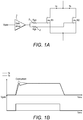
- FIG. 1A A conventional, parallel-connected switching arrangement as described above is shown in Fig. 1A .
- two MOSFETS M1, M2 are connected in parallel to the output of a gate driver 2 to which control voltage V gate is applied.
- Other arrangements may use different switching devices such as devices using FET technology, IGBTs etc. and more than two may be provided.
- the switching device outputs are provided to drive a connected load (not shown).
- the load current is shared between the two MOSFETS M1 and M2 (Ia, Ib).
- Ia, Ib As mentioned above, in an ideal situation, la and lb would be equal. In many cases, however, this is not the case, for a number of reasons.
- Gate resistors 3,4 may be connected in series with the MOSFET gates to compensate, to some extent, current imbalance, but, as mentioned in the background, problems still exits.
- the aim of this disclosure is to reduce the difference between currents Ia and Ib, particularly in the transient stage of switch on and switch off.
- the present disclosure provides a method and apparatus to measure the threshold voltage of each of the parallel switching devices at the start up/switch on of the power converter, to compute a time delay between the gate signals of the respective switching devices, in an initial self-calibration process, and to apply this time delay during normal operation of the converter.
- the threshold voltage is derived from the gate current during a specific power up sequence such as shown in Fig. 3 and described further below.
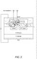
- the input capacitance of a MOSFET varies with gate-to-source voltage as shown in Fig. 2 .
- the threshold voltage V TH At the threshold voltage V TH , there is a discontinuity in the input capacitance and hence the gate current.
- the gate current is measured at the input capacitance discontinuity using known measurement calculations, and from this current, the threshold voltage V TH can be derived. More specifically, it is known that the input capacitance of a MOSFET depends on the thickness of the gate oxide, the threshold voltage and other parameters related to the material of the device.
- the input capacitance depends on the applied voltage and shows a discontinuity when the threshold is reached (see Fig. 2 ). It is therefore possible to indirectly measure the threshold voltage.
- a high pass filter can be applied to the gate current to detect when a spike occurs (indicative of the discontinuity) and the gate-to-source voltage at that time, which will be the threshold voltage, can be recorded. This principle is used to determine the time delay.
- the self-calibration is performed as follows: On power up, at step 100 of Fig. 3 , Vgate is applied to the gate driver 2'. Initially, under the control of a compensator 5, at step 101, all parallel devices except M2 (here M1) are turned ON. Thereafter, M2 is turned on slowly at step 102. This way, the input capacitance of M2 can be extracted since the drain and source are shorted by turning on the MOSFET to be measured. From the gate current, the threshold voltage V TH can be determined as described above at step 103. The measurement is also made for any other switching devices in parallel with M1 (not shown).
- step 104 all parallel switching devices are switched off (step 104) and M2 and, if more than two switching devices are paralleled, all paralleled switches except M1, are turned ON (step 105).
- step 106 A time thereafter, M1 is slowly turned ON at step 106 so that the threshold voltage for M1 can be determined at step 107 (in the same way as above for M2).
- a time delay or slope is computed at step 108 to compensate for the mismatch in threshold voltages, which is the main cause of current imbalances at switch on, and this is used to control the gate driver to compensate for the current imbalance.
- control variable here can be chosen as the compensation of the threshold voltage
Landscapes
- Engineering & Computer Science (AREA)
- Power Engineering (AREA)
- Power Conversion In General (AREA)
Abstract
Description
- The present disclosure is concerned with controlling the switch on of power converters or power switches comprising paralleled switching devices to avoid or minimise current imbalances.
- Power converters find use in many fields for switching power to drive loads. Power converters may comprise networks of parallel and/or series connected power switching devices, particularly semiconductor switching devices such as IGBTs, FETs, MOSFETS and the like the switching of which is controlled by a gate drive.
- Particularly for high power, high current applications, power switching devices are connected in parallel. This allows power losses to be distributed between several devices as well as to achieve high power within the size limitations of such switching devices. Distributing losses between several devices means that there is a lower risk of overheating at the device junction, thus improving the life of the switching devices.
- A problem that has been identified with using paralleled switching devices is that if the devices are not identical (in almost all cases the devices will not be identical due to e.g. manufacturing and material tolerances), the current passing through the respective devices will also not be identical i.e. there may be a current imbalance. This may cause damage to the devices e.g. due to overheating. Even if the devices are nominally equivalent, there may very well be minor differences due to manufacturing tolerances, differences in physical dimensions, age, carrier concentration, materials etc. Alternatively, current imbalances can arise due to different device junction temperatures or gate drive imbalances. Damage can cause a switch to operate outside of its safe operating area.
- Conventionally, this has been compensated by measuring the currents through the respective switching devices and compensate for the differences.
- To compensate for such differences, it has been known to couple a passive component such as an inductor in series with the switching devices to reduce the imbalance in current sharing during transient - i.e. on switching on/power up and also adding in active control devices to counteract imbalances during steady state operation. If the switching devices are MOSFETs, these will also provide some self-balancing of current variation due to their positive temperature coefficient. Adding series inductance impedance in the power path, however, brings its own problems in that it slows down the switching and can generate a ringing effect with the parasitic element of the switching device. This adversely affects the EMI of the power converter.
- It is desired to provide a power converter paralleled switching devices control method and arrangement which overcomes these problems, is non-intrusive, allows lower EMI and provides better control of current imbalance particularly during switching on, but without the need for a complex current system approach.
- In one aspect, the present disclosure provides a method of controlling a power converter having a plurality of parallel-connected switching devices, the method comprising:
- measuring a threshold voltage of each of the parallel switching devices at start up of the parallel power converter in an initial self-calibration process; and
- determining synchronization of a time at which the threshold voltages of the respective switching devices occur.
- In another aspect, there is provided a system for controlling a power converter having a plurality of parallel-connected switching devices, the system comprising:
- means for measuring a threshold voltage of each of the parallel switching devices at start up of the parallel power converter in an initial self-calibration process; and
- means for determining synchronization of a time at which the threshold voltages of the respective switching devices occur.
- Preferred embodiments will now be described, by way of example only, with reference to the accompanying drawings.
-
-
Fig. 1A is a schematic circuit diagram of a power switching circuit as known in the prior art. -
Fig. 1B shows the variation of current through the respective switching devices over time for the arrangement ofFig. 1A . -
Fig. 1C is a schematic circuit diagram of a power switching circuit modified according to the present disclosure. -
Fig. 1D shows the variation of current through the respective switching devices over time for the arrangement ofFig. 1C . -
Fig. 2 illustrates the variation in input capacitance with gate-to-source voltage for a D- MOSFET. -
Fig. 3 is a flow chart showing the sequence of threshold voltage compensation for an arrangement such as shown inFig. 1C . - A conventional, parallel-connected switching arrangement as described above is shown in
Fig. 1A . Here, two MOSFETS M1, M2 are connected in parallel to the output of agate driver 2 to which control voltage Vgate is applied. Other arrangements may use different switching devices such as devices using FET technology, IGBTs etc. and more than two may be provided. The switching device outputs are provided to drive a connected load (not shown). The load current is shared between the two MOSFETS M1 and M2 (Ia, Ib). As mentioned above, in an ideal situation, la and lb would be equal. In many cases, however, this is not the case, for a number of reasons.Gate resistors - The current imbalance, particular in the transient state on switching on, can be seen in
Fig. 1B . When the gate voltage Vgate is applied (at the time the Vgate line rises vertically in the lower part of the graph) current starts to flow through each of the switching devices M1 and M2 when their respective threshold voltage is crossed. Because, however, the devices are not identical, la and lb will also not be identical, as can be seen in the top part of the graph. When the switches reach steady state, la and lb will approach each other. The problem of current imbalance is, therefore, mainly at switch on and switch off. - The aim of this disclosure is to reduce the difference between currents Ia and Ib, particularly in the transient stage of switch on and switch off. To do this, the present disclosure provides a method and apparatus to measure the threshold voltage of each of the parallel switching devices at the start up/switch on of the power converter, to compute a time delay between the gate signals of the respective switching devices, in an initial self-calibration process, and to apply this time delay during normal operation of the converter. The threshold voltage is derived from the gate current during a specific power up sequence such as shown in
Fig. 3 and described further below. - The input capacitance of a MOSFET varies with gate-to-source voltage as shown in
Fig. 2 . At the threshold voltage VTH, there is a discontinuity in the input capacitance and hence the gate current. Using this, the gate current is measured at the input capacitance discontinuity using known measurement calculations, and from this current, the threshold voltage VTH can be derived. More specifically, it is known that the input capacitance of a MOSFET depends on the thickness of the gate oxide, the threshold voltage and other parameters related to the material of the device. The input capacitance depends on the applied voltage and shows a discontinuity when the threshold is reached (seeFig. 2 ). It is therefore possible to indirectly measure the threshold voltage. For example, a high pass filter can be applied to the gate current to detect when a spike occurs (indicative of the discontinuity) and the gate-to-source voltage at that time, which will be the threshold voltage, can be recorded. This principle is used to determine the time delay. - Operation of the control according to the disclosure will now be described with reference to
Figs. 1C, 1D andFig. 3 . - According to the present disclosure, the self-calibration is performed as follows: On power up, at
step 100 ofFig. 3 , Vgate is applied to the gate driver 2'. Initially, under the control of acompensator 5, atstep 101, all parallel devices except M2 (here M1) are turned ON. Thereafter, M2 is turned on slowly atstep 102. This way, the input capacitance of M2 can be extracted since the drain and source are shorted by turning on the MOSFET to be measured. From the gate current, the threshold voltage VTH can be determined as described above atstep 103. The measurement is also made for any other switching devices in parallel with M1 (not shown). - Next, all parallel switching devices are switched off (step 104) and M2 and, if more than two switching devices are paralleled, all paralleled switches except M1, are turned ON (step 105). A time thereafter, M1 is slowly turned ON at
step 106 so that the threshold voltage for M1 can be determined at step 107 (in the same way as above for M2). Based on the difference between the threshold voltages for the all of the parallel switching devices M1, M2 a time delay or slope is computed atstep 108 to compensate for the mismatch in threshold voltages, which is the main cause of current imbalances at switch on, and this is used to control the gate driver to compensate for the current imbalance. - The above example describes driving the gates with a voltage source, but the gates can also be driven by a current source. When driven by a voltage source, the turn-on time instant can be derived from the following equation :

- R - Gate resistance
- C - input capacitance of the MOSFET
- Vth - Threshold voltage of theMOSFET
- Vgs,max - Maximum input gate source voltage
- There are different ways to match the turn-on instant of the devices to the threshold voltage i.e. to match t Vgs=Vth of each paralleled MOSFET. One method is creating a time delay (tdelay ) between the different t Vgs=Vth of each MOSFET to synchronize the turn-on time.
- 1. R variation : as per the equation above, the synchronization of t Vgs=Vth can be achieved by changing the value of R (this is described in Japanese patent
JP2014230307A - 2. C variation: it can also be implemented by adding external voltage controlled capacitance at the input of gate and source of the MOSFET and applying a control-bias voltage on the capacitor which effectively changes the value of C in real-time to synchronize the turn-on times of the MOSFET.
- 3. Vgsmax variation: the turn-on time of paralleled MOSFET can be synchronized by varying the input voltage Vgs,max until the turn-on occurs and then keep the value of Vgs,max constant for all the paralleled MOSFET.
- It is also possible to drive the gate source with a current source and the resulting equation for turn-on time at which the threshold voltage on the MOSFET is impressed is given by the equation

- C - input capacitance of the MOSFET
- Vth - Threshold voltage of the MOSFET
- Ig - Charging current to the input capacitance
- It is simple to compensate the threshold voltage mismatch and synchronize the turn-on time of the paralleled MOSFET by controlling the charge injected into the capacitance C by controlling the input current Ig for each MOSFET.
- There are multiple ways to implement a controlled current source where the control variable here can be chosen as the compensation of the threshold voltage.
Claims (5)
- A method of controlling a power converter having a plurality of parallel-connected switching devices, the method comprising:measuring a threshold voltage of each of the parallel switching devices at start up of the parallel power converter in an initial self-calibration process; anddetermining synchronization of a time at which the threshold voltages of the respective switching devices occur.
- A system for controlling a power converter having a plurality of parallel-connected switching devices, the system comprising:means for measuring a threshold voltage of each of the parallel switching devices at start up of the parallel power converter in an initial self-calibration process; andmeans for determining synchronization of a time at which the threshold voltages of the respective switching devices occur.
- The method of claim 1, wherein the initial self-calibration process comprises, on power up of the power converter:i) turning on all parallel-connected switching devices except one of said devices;ii) thereafter, gradually turning said one device on; andiii) extracting the threshold voltage of said one device; andiv) repeating steps i) to iii) for each of the parallel-connected switching devices as said one device; and wherein the synchronisation is determined from differences in the derived threshold voltages.
- The method of claim 3, wherein the synchronised turn-on time is determined from the following equation :
 R - Gate resistanceC - input capacitance of the MOSFETVth - Threshold voltage of theMOSFETVgs,max - Maximum input gate source voltage
 - The method of claim 4, wherein the synchronized turn-on time is determined by varying C by adding external voltage controlled capacitance at the input of the respective switching device and applying a control-bias voltage on the capacitor to effectively change the value of C in real-time to synchronize the turn-on time of the switching device.
Applications Claiming Priority (1)
| Application Number | Priority Date | Filing Date | Title |
|---|---|---|---|
| IN201811002318 | 2018-01-19 |
Publications (2)
| Publication Number | Publication Date |
|---|---|
| EP3514929A1 true EP3514929A1 (en) | 2019-07-24 |
| EP3514929B1 EP3514929B1 (en) | 2021-02-24 |
Family
ID=63012930
Family Applications (1)
| Application Number | Title | Priority Date | Filing Date |
|---|---|---|---|
| EP18184523.1A Active EP3514929B1 (en) | 2018-01-19 | 2018-07-19 | Parallel switch current control |
Country Status (2)
| Country | Link |
|---|---|
| US (1) | US10686439B2 (en) |
| EP (1) | EP3514929B1 (en) |
Cited By (3)
| Publication number | Priority date | Publication date | Assignee | Title |
|---|---|---|---|---|
| US12562727B2 (en) | 2024-03-20 | 2026-02-24 | GM Global Technology Operations LLC | Variable slew-rate current source gate drivers for hybrid power modules |
| DE102024138202A1 (en) * | 2024-10-29 | 2026-04-30 | GM Global Technology Operations LLC | Hybrid gate drivers with variable slew rate for power modules |
| DE102024210760A1 (en) * | 2024-11-08 | 2026-05-13 | Robert Bosch Gesellschaft mit beschränkter Haftung | Method for synchronizing the switch-on process of parallel-connected transistors |
Families Citing this family (2)
| Publication number | Priority date | Publication date | Assignee | Title |
|---|---|---|---|---|
| EP4325712A1 (en) | 2022-08-16 | 2024-02-21 | Raytheon Technologies Research Centre Ireland, Limited | Control structures for parallel motor drive control architectures |
| CN117543966A (en) * | 2023-11-08 | 2024-02-09 | 台达电子企业管理(上海)有限公司 | Power switch circuit and control method thereof |
Citations (1)
| Publication number | Priority date | Publication date | Assignee | Title |
|---|---|---|---|---|
| JP2014230307A (en) | 2013-05-17 | 2014-12-08 | 富士電機株式会社 | Electric power conversion system |
Family Cites Families (11)
| Publication number | Priority date | Publication date | Assignee | Title |
|---|---|---|---|---|
| US5051603A (en) * | 1990-08-14 | 1991-09-24 | General Electric Company | Method and apparatus for matching turn-off times of parallel connected semiconductor switching devices |
| JP3267189B2 (en) * | 1997-05-14 | 2002-03-18 | 富士電機株式会社 | Device steady-state current balance control circuit of power converter |
| WO2002052726A1 (en) * | 2000-12-27 | 2002-07-04 | Ct-Concept Technologie Ag | Method for the dynamic balancing of series- and parallel-wired power semiconductor circuits |
| EP2424112B1 (en) * | 2010-08-23 | 2015-07-01 | ABB Research Ltd | Current balancing of parallel connected semiconductor components |
| EP2445110B1 (en) * | 2010-10-22 | 2014-05-14 | ABB Research Ltd | Gate driver unit for electrical switching device |
| GB2497967B (en) * | 2011-12-23 | 2018-02-21 | Reinhausen Maschf Scheubeck | Fault-tolerant control systems |
| GB201311997D0 (en) * | 2013-07-04 | 2013-08-21 | Amantys Ltd | Synchronising parallel power switches |
| US9804613B2 (en) * | 2013-07-22 | 2017-10-31 | The Boeing Company | Parallel transistor circuit controller |
| EP2884661B1 (en) * | 2013-12-11 | 2019-02-06 | ABB Schweiz AG | Method and apparatus for balancing currents |
| US9800132B2 (en) * | 2015-12-29 | 2017-10-24 | General Electric Company | Systems and methods for controlling a plurality of power semiconductor devices |
| EP3512083B1 (en) * | 2018-01-12 | 2023-08-23 | ABB Schweiz AG | Determining and compensating power transistor switching delay |
-
2018
- 2018-07-19 EP EP18184523.1A patent/EP3514929B1/en active Active
- 2018-11-16 US US16/192,949 patent/US10686439B2/en active Active
Patent Citations (1)
| Publication number | Priority date | Publication date | Assignee | Title |
|---|---|---|---|---|
| JP2014230307A (en) | 2013-05-17 | 2014-12-08 | 富士電機株式会社 | Electric power conversion system |
Non-Patent Citations (2)
| Title |
|---|
| BORTIS D ET AL: "Active Gate Control for Current Balancing of Parallel-Connected IGBT Modules in Solid-State Modulators", IEEE TRANSACTIONS ON PLASMA SCIENCE, IEEE SERVICE CENTER, PISCATAWAY, NJ, US, vol. 36, no. 5, 1 October 2008 (2008-10-01), pages 2632 - 2637, XP011237226, ISSN: 0093-3813, DOI: 10.1109/TPS.2008.2003971 * |
| HOFER P ET AL: "Paralleling intelligent IGBT power modules with active gate-controlled current balancing", 23 June 1996 (1996-06-23), XP002619276, ISBN: 978-0-7803-3501-1, Retrieved from the Internet <URL:http://ieeexplore.ieee.org/stamp/stamp.jsp?tp=&arnumber=548751&tag=1> [retrieved on 20110128] * |
Cited By (3)
| Publication number | Priority date | Publication date | Assignee | Title |
|---|---|---|---|---|
| US12562727B2 (en) | 2024-03-20 | 2026-02-24 | GM Global Technology Operations LLC | Variable slew-rate current source gate drivers for hybrid power modules |
| DE102024138202A1 (en) * | 2024-10-29 | 2026-04-30 | GM Global Technology Operations LLC | Hybrid gate drivers with variable slew rate for power modules |
| DE102024210760A1 (en) * | 2024-11-08 | 2026-05-13 | Robert Bosch Gesellschaft mit beschränkter Haftung | Method for synchronizing the switch-on process of parallel-connected transistors |
Also Published As
| Publication number | Publication date |
|---|---|
| US20190229722A1 (en) | 2019-07-25 |
| EP3514929B1 (en) | 2021-02-24 |
| US10686439B2 (en) | 2020-06-16 |
Similar Documents
| Publication | Publication Date | Title |
|---|---|---|
| US10686439B2 (en) | Parallel switch current control | |
| Xue et al. | Active compensation of current unbalance in paralleled silicon carbide MOSFETs | |
| CN108696108B (en) | Device and method for monitoring current and power conversion system | |
| WO2012141859A2 (en) | Cascode switches including normally-off and normally-on devices and circuits comprising the switches | |
| US20210399724A1 (en) | Gate voltage magnitude compensation equalization method and circuit for series operation of power switch transistors | |
| WO2005104743A3 (en) | Adaptive gate drive for switching devices of inverter | |
| Nguyen et al. | Analytic model for power MOSFET turn-off switching loss under the effect of significant current diversion at fast switching events | |
| WO2019142585A1 (en) | Power conversion device | |
| US8614905B2 (en) | Voltage converting apparatus and method for converting a voltage | |
| Shojaie et al. | Design and experimental verification of a high-voltage series-stacked GaN eHEMT module for electric vehicle applications | |
| EP3076549A1 (en) | Gate drive circuit and intelligent power module | |
| Li et al. | Medium voltage power switch based on SiC JFETs | |
| Kinzer | Monolithic GaN power IC technology drives wide bandgap adoption | |
| US11415625B2 (en) | Device and method for monitoring multi-die power module | |
| Lee et al. | Active gate control for series connected SiC MOSFETs | |
| Barchowsky et al. | Analytical and experimental optimization of external gate resistance for safe rapid turn on of normally off GaN HFETs | |
| US20110204835A1 (en) | Switching circuit for series configuration of igbt transistors | |
| Lee et al. | Voltage balancing control with active gate driver for series connected SiC MOSFETs | |
| Shojaie et al. | Design of an all-GaN bidirectional DC-DC converter for medium voltage DC ship power systems using series-stacked GaN modules | |
| Li et al. | Series-connection of SiC normally-on JFETs | |
| Ramachandran et al. | Switching losses in a 1.7 kW GaN based full-bridge DC-DC converter with synchronous rectification | |
| Huang et al. | A smart silicon carbide LED driver IC with integrated dual-level condition-monitoring mechanism | |
| CN109752638B (en) | Device and method for continuously measuring output curve of IGBT (insulated Gate Bipolar transistor) chip | |
| US10622991B2 (en) | Switch driver | |
| Pal et al. | Comparative study of enhancement-mode gallium nitride FETs and silicon MOSFETs for power electronic applications |
Legal Events
| Date | Code | Title | Description |
|---|---|---|---|
| PUAI | Public reference made under article 153(3) epc to a published international application that has entered the european phase |
Free format text: ORIGINAL CODE: 0009012 |
|
| STAA | Information on the status of an ep patent application or granted ep patent |
Free format text: STATUS: THE APPLICATION HAS BEEN PUBLISHED |
|
| AK | Designated contracting states |
Kind code of ref document: A1 Designated state(s): AL AT BE BG CH CY CZ DE DK EE ES FI FR GB GR HR HU IE IS IT LI LT LU LV MC MK MT NL NO PL PT RO RS SE SI SK SM TR |
|
| AX | Request for extension of the european patent |
Extension state: BA ME |
|
| STAA | Information on the status of an ep patent application or granted ep patent |
Free format text: STATUS: REQUEST FOR EXAMINATION WAS MADE |
|
| 17P | Request for examination filed |
Effective date: 20191118 |
|
| RBV | Designated contracting states (corrected) |
Designated state(s): AL AT BE BG CH CY CZ DE DK EE ES FI FR GB GR HR HU IE IS IT LI LT LU LV MC MK MT NL NO PL PT RO RS SE SI SK SM TR |
|
| GRAP | Despatch of communication of intention to grant a patent |
Free format text: ORIGINAL CODE: EPIDOSNIGR1 |
|
| STAA | Information on the status of an ep patent application or granted ep patent |
Free format text: STATUS: GRANT OF PATENT IS INTENDED |
|
| INTG | Intention to grant announced |
Effective date: 20200424 |
|
| GRAS | Grant fee paid |
Free format text: ORIGINAL CODE: EPIDOSNIGR3 |
|
| GRAA | (expected) grant |
Free format text: ORIGINAL CODE: 0009210 |
|
| STAA | Information on the status of an ep patent application or granted ep patent |
Free format text: STATUS: THE PATENT HAS BEEN GRANTED |
|
| AK | Designated contracting states |
Kind code of ref document: B1 Designated state(s): AL AT BE BG CH CY CZ DE DK EE ES FI FR GB GR HR HU IE IS IT LI LT LU LV MC MK MT NL NO PL PT RO RS SE SI SK SM TR |
|
| REG | Reference to a national code |
Ref country code: CH Ref legal event code: EP |
|
| REG | Reference to a national code |
Ref country code: AT Ref legal event code: REF Ref document number: 1365735 Country of ref document: AT Kind code of ref document: T Effective date: 20210315 |
|
| REG | Reference to a national code |
Ref country code: IE Ref legal event code: FG4D |
|
| REG | Reference to a national code |
Ref country code: DE Ref legal event code: R096 Ref document number: 602018012927 Country of ref document: DE |
|
| REG | Reference to a national code |
Ref country code: LT Ref legal event code: MG9D |
|
| REG | Reference to a national code |
Ref country code: NL Ref legal event code: MP Effective date: 20210224 |
|
| PG25 | Lapsed in a contracting state [announced via postgrant information from national office to epo] |
Ref country code: NO Free format text: LAPSE BECAUSE OF FAILURE TO SUBMIT A TRANSLATION OF THE DESCRIPTION OR TO PAY THE FEE WITHIN THE PRESCRIBED TIME-LIMIT Effective date: 20210524 Ref country code: PT Free format text: LAPSE BECAUSE OF FAILURE TO SUBMIT A TRANSLATION OF THE DESCRIPTION OR TO PAY THE FEE WITHIN THE PRESCRIBED TIME-LIMIT Effective date: 20210624 Ref country code: LT Free format text: LAPSE BECAUSE OF FAILURE TO SUBMIT A TRANSLATION OF THE DESCRIPTION OR TO PAY THE FEE WITHIN THE PRESCRIBED TIME-LIMIT Effective date: 20210224 Ref country code: HR Free format text: LAPSE BECAUSE OF FAILURE TO SUBMIT A TRANSLATION OF THE DESCRIPTION OR TO PAY THE FEE WITHIN THE PRESCRIBED TIME-LIMIT Effective date: 20210224 Ref country code: FI Free format text: LAPSE BECAUSE OF FAILURE TO SUBMIT A TRANSLATION OF THE DESCRIPTION OR TO PAY THE FEE WITHIN THE PRESCRIBED TIME-LIMIT Effective date: 20210224 Ref country code: GR Free format text: LAPSE BECAUSE OF FAILURE TO SUBMIT A TRANSLATION OF THE DESCRIPTION OR TO PAY THE FEE WITHIN THE PRESCRIBED TIME-LIMIT Effective date: 20210525 Ref country code: BG Free format text: LAPSE BECAUSE OF FAILURE TO SUBMIT A TRANSLATION OF THE DESCRIPTION OR TO PAY THE FEE WITHIN THE PRESCRIBED TIME-LIMIT Effective date: 20210524 |
|
| REG | Reference to a national code |
Ref country code: AT Ref legal event code: MK05 Ref document number: 1365735 Country of ref document: AT Kind code of ref document: T Effective date: 20210224 |
|
| PG25 | Lapsed in a contracting state [announced via postgrant information from national office to epo] |
Ref country code: RS Free format text: LAPSE BECAUSE OF FAILURE TO SUBMIT A TRANSLATION OF THE DESCRIPTION OR TO PAY THE FEE WITHIN THE PRESCRIBED TIME-LIMIT Effective date: 20210224 Ref country code: PL Free format text: LAPSE BECAUSE OF FAILURE TO SUBMIT A TRANSLATION OF THE DESCRIPTION OR TO PAY THE FEE WITHIN THE PRESCRIBED TIME-LIMIT Effective date: 20210224 Ref country code: NL Free format text: LAPSE BECAUSE OF FAILURE TO SUBMIT A TRANSLATION OF THE DESCRIPTION OR TO PAY THE FEE WITHIN THE PRESCRIBED TIME-LIMIT Effective date: 20210224 Ref country code: LV Free format text: LAPSE BECAUSE OF FAILURE TO SUBMIT A TRANSLATION OF THE DESCRIPTION OR TO PAY THE FEE WITHIN THE PRESCRIBED TIME-LIMIT Effective date: 20210224 Ref country code: SE Free format text: LAPSE BECAUSE OF FAILURE TO SUBMIT A TRANSLATION OF THE DESCRIPTION OR TO PAY THE FEE WITHIN THE PRESCRIBED TIME-LIMIT Effective date: 20210224 |
|
| PG25 | Lapsed in a contracting state [announced via postgrant information from national office to epo] |
Ref country code: IS Free format text: LAPSE BECAUSE OF FAILURE TO SUBMIT A TRANSLATION OF THE DESCRIPTION OR TO PAY THE FEE WITHIN THE PRESCRIBED TIME-LIMIT Effective date: 20210624 |
|
| PG25 | Lapsed in a contracting state [announced via postgrant information from national office to epo] |
Ref country code: SM Free format text: LAPSE BECAUSE OF FAILURE TO SUBMIT A TRANSLATION OF THE DESCRIPTION OR TO PAY THE FEE WITHIN THE PRESCRIBED TIME-LIMIT Effective date: 20210224 Ref country code: AT Free format text: LAPSE BECAUSE OF FAILURE TO SUBMIT A TRANSLATION OF THE DESCRIPTION OR TO PAY THE FEE WITHIN THE PRESCRIBED TIME-LIMIT Effective date: 20210224 Ref country code: EE Free format text: LAPSE BECAUSE OF FAILURE TO SUBMIT A TRANSLATION OF THE DESCRIPTION OR TO PAY THE FEE WITHIN THE PRESCRIBED TIME-LIMIT Effective date: 20210224 Ref country code: CZ Free format text: LAPSE BECAUSE OF FAILURE TO SUBMIT A TRANSLATION OF THE DESCRIPTION OR TO PAY THE FEE WITHIN THE PRESCRIBED TIME-LIMIT Effective date: 20210224 |
|
| REG | Reference to a national code |
Ref country code: DE Ref legal event code: R097 Ref document number: 602018012927 Country of ref document: DE |
|
| PG25 | Lapsed in a contracting state [announced via postgrant information from national office to epo] |
Ref country code: RO Free format text: LAPSE BECAUSE OF FAILURE TO SUBMIT A TRANSLATION OF THE DESCRIPTION OR TO PAY THE FEE WITHIN THE PRESCRIBED TIME-LIMIT Effective date: 20210224 Ref country code: DK Free format text: LAPSE BECAUSE OF FAILURE TO SUBMIT A TRANSLATION OF THE DESCRIPTION OR TO PAY THE FEE WITHIN THE PRESCRIBED TIME-LIMIT Effective date: 20210224 Ref country code: SK Free format text: LAPSE BECAUSE OF FAILURE TO SUBMIT A TRANSLATION OF THE DESCRIPTION OR TO PAY THE FEE WITHIN THE PRESCRIBED TIME-LIMIT Effective date: 20210224 |
|
| PLBE | No opposition filed within time limit |
Free format text: ORIGINAL CODE: 0009261 |
|
| STAA | Information on the status of an ep patent application or granted ep patent |
Free format text: STATUS: NO OPPOSITION FILED WITHIN TIME LIMIT |
|
| PG25 | Lapsed in a contracting state [announced via postgrant information from national office to epo] |
Ref country code: ES Free format text: LAPSE BECAUSE OF FAILURE TO SUBMIT A TRANSLATION OF THE DESCRIPTION OR TO PAY THE FEE WITHIN THE PRESCRIBED TIME-LIMIT Effective date: 20210224 Ref country code: AL Free format text: LAPSE BECAUSE OF FAILURE TO SUBMIT A TRANSLATION OF THE DESCRIPTION OR TO PAY THE FEE WITHIN THE PRESCRIBED TIME-LIMIT Effective date: 20210224 |
|
| 26N | No opposition filed |
Effective date: 20211125 |
|
| PG25 | Lapsed in a contracting state [announced via postgrant information from national office to epo] |
Ref country code: SI Free format text: LAPSE BECAUSE OF FAILURE TO SUBMIT A TRANSLATION OF THE DESCRIPTION OR TO PAY THE FEE WITHIN THE PRESCRIBED TIME-LIMIT Effective date: 20210224 |
|
| REG | Reference to a national code |
Ref country code: CH Ref legal event code: PL |
|
| PG25 | Lapsed in a contracting state [announced via postgrant information from national office to epo] |
Ref country code: MC Free format text: LAPSE BECAUSE OF FAILURE TO SUBMIT A TRANSLATION OF THE DESCRIPTION OR TO PAY THE FEE WITHIN THE PRESCRIBED TIME-LIMIT Effective date: 20210224 |
|
| REG | Reference to a national code |
Ref country code: BE Ref legal event code: MM Effective date: 20210731 |
|
| PG25 | Lapsed in a contracting state [announced via postgrant information from national office to epo] |
Ref country code: LI Free format text: LAPSE BECAUSE OF NON-PAYMENT OF DUE FEES Effective date: 20210731 Ref country code: IT Free format text: LAPSE BECAUSE OF FAILURE TO SUBMIT A TRANSLATION OF THE DESCRIPTION OR TO PAY THE FEE WITHIN THE PRESCRIBED TIME-LIMIT Effective date: 20210224 Ref country code: CH Free format text: LAPSE BECAUSE OF NON-PAYMENT OF DUE FEES Effective date: 20210731 |
|
| PG25 | Lapsed in a contracting state [announced via postgrant information from national office to epo] |
Ref country code: IS Free format text: LAPSE BECAUSE OF FAILURE TO SUBMIT A TRANSLATION OF THE DESCRIPTION OR TO PAY THE FEE WITHIN THE PRESCRIBED TIME-LIMIT Effective date: 20210624 Ref country code: LU Free format text: LAPSE BECAUSE OF NON-PAYMENT OF DUE FEES Effective date: 20210719 |
|
| PG25 | Lapsed in a contracting state [announced via postgrant information from national office to epo] |
Ref country code: IE Free format text: LAPSE BECAUSE OF NON-PAYMENT OF DUE FEES Effective date: 20210719 Ref country code: BE Free format text: LAPSE BECAUSE OF NON-PAYMENT OF DUE FEES Effective date: 20210731 |
|
| P01 | Opt-out of the competence of the unified patent court (upc) registered |
Effective date: 20230522 |
|
| PG25 | Lapsed in a contracting state [announced via postgrant information from national office to epo] |
Ref country code: CY Free format text: LAPSE BECAUSE OF FAILURE TO SUBMIT A TRANSLATION OF THE DESCRIPTION OR TO PAY THE FEE WITHIN THE PRESCRIBED TIME-LIMIT Effective date: 20210224 |
|
| PG25 | Lapsed in a contracting state [announced via postgrant information from national office to epo] |
Ref country code: HU Free format text: LAPSE BECAUSE OF FAILURE TO SUBMIT A TRANSLATION OF THE DESCRIPTION OR TO PAY THE FEE WITHIN THE PRESCRIBED TIME-LIMIT; INVALID AB INITIO Effective date: 20180719 |
|
| PG25 | Lapsed in a contracting state [announced via postgrant information from national office to epo] |
Ref country code: MK Free format text: LAPSE BECAUSE OF FAILURE TO SUBMIT A TRANSLATION OF THE DESCRIPTION OR TO PAY THE FEE WITHIN THE PRESCRIBED TIME-LIMIT Effective date: 20210224 |
|
| PG25 | Lapsed in a contracting state [announced via postgrant information from national office to epo] |
Ref country code: MT Free format text: LAPSE BECAUSE OF FAILURE TO SUBMIT A TRANSLATION OF THE DESCRIPTION OR TO PAY THE FEE WITHIN THE PRESCRIBED TIME-LIMIT Effective date: 20210224 |
|
| PGFP | Annual fee paid to national office [announced via postgrant information from national office to epo] |
Ref country code: GB Payment date: 20250619 Year of fee payment: 8 |
|
| PGFP | Annual fee paid to national office [announced via postgrant information from national office to epo] |
Ref country code: FR Payment date: 20250620 Year of fee payment: 8 |
|
| PGFP | Annual fee paid to national office [announced via postgrant information from national office to epo] |
Ref country code: DE Payment date: 20250620 Year of fee payment: 8 |
|
| PG25 | Lapsed in a contracting state [announced via postgrant information from national office to epo] |
Ref country code: TR Free format text: LAPSE BECAUSE OF FAILURE TO SUBMIT A TRANSLATION OF THE DESCRIPTION OR TO PAY THE FEE WITHIN THE PRESCRIBED TIME-LIMIT Effective date: 20210224 |