EP3514899A1 - Lightning arrester - Google Patents
Lightning arrester Download PDFInfo
- Publication number
- EP3514899A1 EP3514899A1 EP17850861.0A EP17850861A EP3514899A1 EP 3514899 A1 EP3514899 A1 EP 3514899A1 EP 17850861 A EP17850861 A EP 17850861A EP 3514899 A1 EP3514899 A1 EP 3514899A1
- Authority
- EP
- European Patent Office
- Prior art keywords
- voltage side
- rod
- end side
- side terminal
- grounded enclosure
- Prior art date
- Legal status (The legal status is an assumption and is not a legal conclusion. Google has not performed a legal analysis and makes no representation as to the accuracy of the status listed.)
- Granted
Links
Images


Classifications
-
- H—ELECTRICITY
- H01—ELECTRIC ELEMENTS
- H01C—RESISTORS
- H01C7/00—Non-adjustable resistors formed as one or more layers or coatings; Non-adjustable resistors made from powdered conducting material or powdered semi-conducting material with or without insulating material
- H01C7/10—Non-adjustable resistors formed as one or more layers or coatings; Non-adjustable resistors made from powdered conducting material or powdered semi-conducting material with or without insulating material voltage responsive, i.e. varistors
- H01C7/12—Overvoltage protection resistors; Arresters
-
- H—ELECTRICITY
- H01—ELECTRIC ELEMENTS
- H01H—ELECTRIC SWITCHES; RELAYS; SELECTORS; EMERGENCY PROTECTIVE DEVICES
- H01H3/00—Mechanisms for operating contacts
- H01H3/32—Driving mechanisms, i.e. for transmitting driving force to the contacts
- H01H3/42—Driving mechanisms, i.e. for transmitting driving force to the contacts using cam or eccentric
-
- G—PHYSICS
- G01—MEASURING; TESTING
- G01R—MEASURING ELECTRIC VARIABLES; MEASURING MAGNETIC VARIABLES
- G01R31/00—Arrangements for testing electric properties; Arrangements for locating electric faults; Arrangements for electrical testing characterised by what is being tested not provided for elsewhere
- G01R31/12—Testing dielectric strength or breakdown voltage ; Testing or monitoring effectiveness or level of insulation, e.g. of a cable or of an apparatus, for example using partial discharge measurements; Electrostatic testing
- G01R31/1227—Testing dielectric strength or breakdown voltage ; Testing or monitoring effectiveness or level of insulation, e.g. of a cable or of an apparatus, for example using partial discharge measurements; Electrostatic testing of components, parts or materials
- G01R31/1254—Testing dielectric strength or breakdown voltage ; Testing or monitoring effectiveness or level of insulation, e.g. of a cable or of an apparatus, for example using partial discharge measurements; Electrostatic testing of components, parts or materials of gas-insulated power appliances or vacuum gaps
-
- H—ELECTRICITY
- H01—ELECTRIC ELEMENTS
- H01C—RESISTORS
- H01C7/00—Non-adjustable resistors formed as one or more layers or coatings; Non-adjustable resistors made from powdered conducting material or powdered semi-conducting material with or without insulating material
- H01C7/18—Non-adjustable resistors formed as one or more layers or coatings; Non-adjustable resistors made from powdered conducting material or powdered semi-conducting material with or without insulating material comprising a plurality of layers stacked between terminals
-
- H—ELECTRICITY
- H01—ELECTRIC ELEMENTS
- H01H—ELECTRIC SWITCHES; RELAYS; SELECTORS; EMERGENCY PROTECTIVE DEVICES
- H01H3/00—Mechanisms for operating contacts
- H01H3/32—Driving mechanisms, i.e. for transmitting driving force to the contacts
- H01H3/46—Driving mechanisms, i.e. for transmitting driving force to the contacts using rod or lever linkage, e.g. toggle
-
- H—ELECTRICITY
- H01—ELECTRIC ELEMENTS
- H01H—ELECTRIC SWITCHES; RELAYS; SELECTORS; EMERGENCY PROTECTIVE DEVICES
- H01H33/00—High-tension or heavy-current switches with arc-extinguishing or arc-preventing means
- H01H33/02—Details
- H01H33/42—Driving mechanisms
-
- H—ELECTRICITY
- H01—ELECTRIC ELEMENTS
- H01T—SPARK GAPS; OVERVOLTAGE ARRESTERS USING SPARK GAPS; SPARKING PLUGS; CORONA DEVICES; GENERATING IONS TO BE INTRODUCED INTO NON-ENCLOSED GASES
- H01T4/00—Overvoltage arresters using spark gaps
- H01T4/04—Housings
-
- H—ELECTRICITY
- H01—ELECTRIC ELEMENTS
- H01T—SPARK GAPS; OVERVOLTAGE ARRESTERS USING SPARK GAPS; SPARKING PLUGS; CORONA DEVICES; GENERATING IONS TO BE INTRODUCED INTO NON-ENCLOSED GASES
- H01T4/00—Overvoltage arresters using spark gaps
- H01T4/16—Overvoltage arresters using spark gaps having a plurality of gaps arranged in series
-
- H—ELECTRICITY
- H02—GENERATION; CONVERSION OR DISTRIBUTION OF ELECTRIC POWER
- H02B—BOARDS, SUBSTATIONS OR SWITCHING ARRANGEMENTS FOR THE SUPPLY OR DISTRIBUTION OF ELECTRIC POWER
- H02B13/00—Arrangement of switchgear in which switches are enclosed in, or structurally associated with, a casing, e.g. cubicle
- H02B13/02—Arrangement of switchgear in which switches are enclosed in, or structurally associated with, a casing, e.g. cubicle with metal casing
- H02B13/035—Gas-insulated switchgear
Definitions
- An embodiment of the present invention relates to a surge arrester.
- a gas-insulation switchgear is subjected to a withstand voltage test at its installed location.
- the test voltage of the withstand voltage test is higher than a voltage applicable to a surge arrester.
- the withstand voltage test is carried out in a state where the surge arrester and the gas-insulation switchgear are electrically disconnected.
- the electrical disconnection between the surge arrester and the gas-insulation switchgear is achieved by, e.g., removing the surge arrester from the gas-insulation switchgear.
- a disconnector is provided in the gas-insulation switchgear, and the disconnector is operated to achieve the electrical disconnection.
- the object of the present invention is to provide a surge arrester capable reducing the work time required for the withstand voltage test and reducing the cost of the entire gas-insulation switchgear.
- a surge arrester has a grounded enclosure, a nonlinear resistor, a high-voltage side terminal part, and a isolating device.
- the grounded enclosure encapsulates therein insulation gas.
- the nonlinear resistor is housed inside the grounded enclosure and has a high-voltage side electrode at one end side.
- the high-voltage side terminal part is installed at the one end side in the grounded enclosure and electrically connected to a gas-insulation switchgear.
- the isolating device has a guide conductor and a movable rod and is configured to electrically connect or electrically disconnect the high-voltage side terminal part and the high-voltage side electrode.
- the high-voltage side terminal part has a concave part at the other end side.
- the guide conductor is electrically connected to the high-voltage side electrode inside the grounded enclosure and formed such that a guide conductor through hole faces the concave part of the high-voltage side terminal part.
- the movable rod is inserted through the guide conductor through hole and configured to be movable between the one end side and the other end side.
- the isolating device moves the movable rod to the one end side when the high-voltage side terminal part and the high-voltage side electrode are electrically connected to house a part of the movable rod in the concave part of the high-voltage side terminal part and moves the movable rod to the other end side when the high-voltage side terminal part and the high-voltage side electrode are electrically disconnected to separate the movable rod and the high-voltage side terminal part from each other.
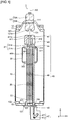
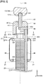
- FIGS. 1 to 5 are cross-sectional views illustrating a surge arrester 1 according to an embodiment of the present invention.
- FIGS. 1 to 3 illustrate the vertical surface (xz plane) of the surge arrester 1 extending along the vertical direction z.
- the surge arrester 1 according to the present embodiment is a tank-shaped surge arrester installed in a gas-insulation switchgear (not illustrated).
- FIG. 1 the state of the surge arrester 1 when the gas-insulation switchgear is subjected to a withstand voltage test is illustrated.
- FIG. 2 shows the state of the surge arrester 1 being used as a protecting device for protecting a gas-insulation switchgear from abnormal voltage (surge voltage) due to, e.g., lightning.
- FIG 3 is a partially enlarged view of FIG 2 .
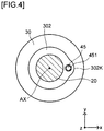
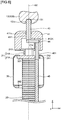
- FIGS 4 and 5 illustrate the horizontal surface (xy plane) perpendicular to the vertical direction z of the surge arrester 1.
- FIG 4 is a cross-sectional view taken along line Z1-Z1 in FIG. 3
- FIG 5 is a cross-sectional view taken along line Z2-Z2 in FIG 3 .
- the surge arrester 1 includes a grounded enclosure 10, a nonlinear resistor 20 (internal element), a shield 30, and a isolating device 40.
- a grounded enclosure 10 a nonlinear resistor 20 (internal element)
- a shield 30 a shield 30
- a isolating device 40 a shield 40 for protecting the surge arrester 1 from the outside environment.
- the grounded enclosure 10 is a cylindrical tubular body made of a metal material and is installed such that a center axis AX (tube axis) extends in the vertical direction z.
- the grounded enclosure 10 has a tank upper opening 101 at the upper surface thereof and a tank lower opening 102 at the lower surface thereof.
- the tank upper opening 101 is closed by an insulating spacer 11, a ring 12, and a high-voltage side terminal part 13 (high-voltage side conductor) which are provided at the upper surface of the grounded enclosure 10.
- the insulating spacer 11 is a disk-shaped member having the center part thereof protruding outward and is installed coaxially with the grounded enclosure 10. That is, the center axis (not illustrated) of the insulating spacer 11 coincides with the center axis AX of the grounded enclosure 10.
- the ring 12 is installed so as to surround the center portion of the insulating spacer 11, whereby the insulating spacer 11 is fixed to the upper side of the grounded enclosure 10.
- a metal conductor 111 is provided at the center portion of the insulating spacer 11, and an insulating body such as epoxy resin is formed around the metal conductor 111.
- the insulating spacer 11 may have a shape in which the center portion thereof protrudes inward.
- the high-voltage side terminal part 13 includes a first high-voltage side terminal component 13A and a second high-voltage side terminal component 13B.
- the first high-voltage side terminal component 13A and the second high-voltage side terminal component 13B are conductors each having a horizontal surface that is perpendicular to the center axis AX of the grounded enclosure 10 and circular in cross section.
- the first and second high-voltage side terminal components 13A and 13B are installed coaxially with the grounded enclosure 10.
- the first high-voltage side terminal component 13A of the high-voltage side terminal part 13 is installed on the upper surface of the metal conductor 111 provided at the center of the insulating spacer 11.
- the first high-voltage side terminal component 13A is electrically connected, at its upper-side portion, to the bus line (not illustrated) of the gas-insulation switchgear.
- the second high-voltage side terminal component 13B of the high-voltage side terminal part 13 is installed on the lower surface of the metal conductor 111.
- the first high-voltage side terminal component 13A and the second high-voltage side terminal component 13B are fixed to the metal conductor 111 using, e.g., a bolt (not illustrated) and thus electrically connected to each other through the metal conductor 111.
- a concave part 131 is formed in the surface on the lower end (the other end) of the second high-voltage side terminal component 13B, and a first contact 131 c is provided along the inner peripheral surface of the concave part 131.
- the tank lower opening 102 of the grounded enclosure 10 is closed by a bottom plate 15 provided at the lower surface of the grounded enclosure 10.
- the bottom plate 15 is a disk-shaped conductor through which a first bottom plate through hole 151 and a second bottom plate through hole 152 penetrate in the vertical direction z.
- the first bottom plate through hole 151 and the second bottom plate through hole 152 are not formed coaxially with the grounded enclosure 10 but formed at an eccentric position from the center axis AX of the grounded enclosure 10.
- a ground side terminal part 221 is inserted through the first bottom plate through hole 151, and an operating rod 46 constituting the isolating device 40 is inserted through the second bottom plate through hole 152.
- the insulating spacer 11 and high-voltage side terminal part 13, and the like are provided on the upper end (one end) side of the grounded enclosure 10, and the bottom plate 15, ground side terminal part 221, and the like are provided on the other end side thereof, whereby the grounded enclosure 10 has a hermetically sealed inner space.
- Insulation gas such as SF 6 gas is encapsulated in the hermetically sealed space.
- the nonlinear resistor 20 has a disk-like shape, and a plurality of the nonlinear resistors 20 are laminated in the vertical direction z.
- the nonlinear resistor 20 is an element mainly including, e.g., zinc oxide.
- the nonlinear resistor 20 exhibits an insulation property when normal voltage acts thereon; while when abnormal voltage which is higher than the normal voltage acts on the nonlinear resistor 20, it is reduced in resistance value and thus exhibits a conductive property.
- the laminate formed by laminating the plurality of nonlinear resistors 20 is housed inside the grounded enclosure 10 as an internal element of the surge arrester 1.
- the laminate of the nonlinear resistors 20 is coaxial with the grounded enclosure 10.
- the laminate has a high-voltage side electrode 21 (first electrode) on the upper end surface side and a ground side electrode 22 (second electrode) on the lower end surface side.
- the high-voltage side electrode 21 includes a first high-voltage side electrode part 21A and a second high-voltage side electrode part 21B.
- the first high-voltage side electrode part 21A and the second high-voltage side electrode part 21B are integrally formed with each other.
- the first high-voltage side electrode part 21A of the high-voltage side electrode 21 has a disk-like shape, installed coaxially with the grounded enclosure 10, and is larger in outer diameter than the nonlinear resistor 20.
- the first high-voltage side electrode part 21A has a high-voltage side electrode through hole 211 at the outer peripheral portion thereof positioned on the outer peripheral side of the center portion where the nonlinear resistor 20 is disposed.
- the high-voltage side electrode through hole 211 penetrates the first high-voltage side electrode part 21A in a direction along the center axis AX of the grounded enclosure 10.
- the high-voltage side electrode through hole 211 is not formed coaxially with the grounded enclosure 10 but formed in the high-voltage side electrode 21 at an eccentric position from the center axis AX of the grounded enclosure 10.
- a low-friction ring 212 is installed along the inner peripheral surface of the high-voltage side electrode through hole 211.
- the low-friction ring 212 is a ring member made of fluororesin such as polytetrafluoroethylene (PTFE) and has a friction coefficient smaller than that of the inner peripheral surface of the high-voltage side electrode through hole 211.
- the second high-voltage side electrode part 21B of the high-voltage side electrode 21 is a cylindrical tubular body and is installed coaxially with the grounded enclosure 10.
- the second high-voltage side electrode part 21B is positioned on the upper surface side of the first high-voltage side electrode part 21A.
- the second high-voltage side electrode part 21B includes a flange part 213 at the upper surface portion thereof, and the flange part 213 is connected to a guide conductor 41.
- the second high-voltage side electrode part 21B has a high-voltage side electrode opening 214 at the peripheral surface portion thereof.
- the high-voltage side electrode opening 214 makes the inner space of the second high-voltage side electrode part 21B and the outer space thereof communicate with each other in the radial direction of the grounded enclosure 10.
- the ground side electrode 22 is a disk-shaped conductor and is formed such that the ground side terminal part 221 protrudes downward.
- the ground side terminal part 221 is electrically connected to the ground side electrode 22 and is connected to a first bottom plate through hole 151 formed in the bottom plate 15.
- the ground side terminal part 221 is electrically connected to the earth (reference potential point).
- the shield 30 is a cylindrical tubular body made of a conductive material and is installed coaxially with the grounded enclosure 10.
- the shield 30 houses the upper side portion (high-voltage side) of the laminate of the nonlinear resistors 20 in the inner space thereof so as to make the distribution of voltage to be applied to the laminate of the nonlinear resistors 20 uniform in the lamination direction.
- the shield 30 has a shield upper side opening 301 and a shield lower side opening 302.
- the shield upper side opening 301 is a circular opening formed at the upper surface portion of the shield 30, and the inner diameter of the shield upper side opening 301 is smaller than the outer diameter of the high-voltage side electrode 21.
- the shield 30 houses the high-voltage side electrode 21 in the inner space thereof and is supported on the upper surface of the high-voltage side electrode 21.
- the shield lower side opening 302 is a circular opening formed at the lower surface portion of the shield 30, and the inner diameter of the shield lower side opening 302 is larger than the outer diameter of the nonlinear resistor 20.
- the shield lower side opening 302 has a notch 302K (see FIG 4 ) at a portion through which the insulating rod 45 penetrates.
- the isolating device 40 is configured to switch electrically disconnect ( FIG 1 ) or electrically connect ( FIG 2 ) between the high-voltage side terminal part 13 and the high-voltage side electrode 21.
- the isolating device 40 has a guide conductor 41, a movable rod 43, an eccentric member 44, an insulating rod 45, and an operating rod 46 inside the grounded enclosure 10 and has a rod operating part 47 outside the grounded enclosure 10. Details of the above members constituting the isolating device 40 will be described later.
- the guide conductor 41 (internal element side conductor) is a cylindrical tubular body and disposed coaxially with the grounded enclosure 10. Inside the grounded enclosure 10, the guide conductor 41 is disposed closer to the upper end side of the grounded enclosure 10 than the shield 30 is. The guide conductor 41 is supported by the high-voltage side electrode 21. The guide conductor 41 is electrically connected to the high-voltage side electrode 21. The guide conductor 41 faces the high-voltage side terminal part 13 in the vertical direction z with an interval interposed therebetween.
- the guide conductor 41 has a guide conductor through hole 411 and a guide conductor opening 412 which are formed therein.
- the guide conductor through hole 411 is a through hole penetrating the upper surface portion of the guide conductor 41 that faces the high-voltage side terminal part 13 and is coaxial with the concave part 131 of the high-voltage side terminal part 13.
- the inner diameter of the guide conductor through hole 411 and the inner diameter of the concave part 131 formed in the high-voltage side terminal part 13 are equal to each other.
- a second contact 411 c is provided along the inner peripheral surface of the guide conductor through hole 411.
- the guide conductor opening 412 is an opening formed at the peripheral surface portion of the guide conductor 41 and makes the inside of the guide conductor 41 and the outside thereof communicate with each other in the radial direction (x-direction in FIG. 5 ) of the grounded enclosure 10.
- the movable rod 43 is a columnar rod-like body made of a conductive material and is disposed coaxially with the grounded enclosure 10. That is, the movable rod 43 is disposed coaxially with the guide conductor through hole 411 formed in the guide conductor 41 and the concave part 131 formed in the high-voltage side terminal part 13.
- the movable rod 43 can move in the vertical direction z together with the eccentric member 44, insulating rod 45 and operating rod 46 by the operation of the rod operating part 47.
- the movable rod 43 is inserted through the guide conductor through hole 411 of the guide conductor 41 and linearly slid and moved between the upper and lower end sides while being guided by the guide conductor 41 in the vertical direction z.
- the movable rod 43 is moved upward in the vertical direction z, the upper end portion thereof is inserted inside the concave part 131 formed in the high-voltage side terminal part 13.
- the movable rod 43 and the high-voltage side terminal part 13 are separated from each other.
- the eccentric member 44 is a plate-like member (link member) made of a conductive material and is disposed such that the longitudinal direction thereof extends in the radial direction (x-direction in FIG. 5 ) of the grounded enclosure 10. Inside the grounded enclosure 10, the eccentric member 44 connects the movable rod 43 and the insulating rod 45.
- the lower end portion of the movable rod 43 is connected to a part of the upper surface of the eccentric member 44 that is positioned at the center axis AX of the grounded enclosure 10, and the upper end portion of the insulating rod 45 is connected to a part of the lower surface of the eccentric member 44 that is positioned radially outside the center axis AX of the grounded enclosure 10.
- the eccentric member 44 is moved in the vertical direction z in a space including the guide conductor opening 412 and the high-voltage side electrode opening 214.
- the insulating rod 45 is a columnar rod-like body made of an insulating material.
- the insulating rod 45 is made of, e.g., fiber-reinforced plastic (FRP). Unlike the movable rod 43, the insulating rod 45 is not disposed coaxially with the grounded enclosure 10.
- the insulating rod 45 is disposed around the laminate of the nonlinear resistors 20 at an eccentric position from the center axis AX of the grounded enclosure 10 such that the center axis of the insulating rod 45 extends along the vertical direction z. That is, inside the grounded enclosure 10, the insulating rod 45 is disposed at an eccentric position eccentric with respect to the nonlinear resistor 20 and the movable rod 43.
- the insulating rod 45 is disposed such that the upper side portion thereof is inserted through the high-voltage side electrode through hole 211. As described above, the insulating rod 45 is moved in the vertical direction z. A reinforcing part 451 is formed at the upper side portion of the insulating rod 45 where the outer peripheral surface of the rod 45 slides along the inner peripheral surface of the high-voltage side electrode through hole 211 when the rod 45 moves.
- the reinforcing part 451 is made of a metal material to reinforce the sliding portion of the insulating rod 45.
- the outer peripheral surface of the insulating rod 45 contacts the low-friction ring 212 installed inside the high-voltage side electrode through hole 211, allowing the insulating rod 45 to be moved smoothly in the vertical direction z.
- the insulating rod 45 is connected with the operating rod 46 at its lower end portion.
- the operation rod 46 is a columnar rod-like body made of a metal material. Like the insulating rod 45, the operating rod 46 is disposed at an eccentric position from the center axis AX of the grounded enclosure 10 such that the center axis of the insulating rod 45 extends along the vertical direction z.
- the operating rod 46 is inserted through the second bottom plate through hole 152.
- the upper end portion of the operating rod 46 is connected to the insulating rod 45, and the lower end portion thereof is connected to the rod operating part 47.
- At least a part of the operating rod 46 that slides with respect to the bottom plate 15 is made of a metal material for reinforcement.
- the rod operating part 47 is installed outside the grounded enclosure 10.
- the rod operating part 47 is installed at the lower surface of the bottom plate 15.
- the rod operating part 47 includes a plurality of link members (e.g., a first link member 471 and a second link member 472), and the plurality of link members are driven by a driver (not illustrated). With this configuration, the rod operating part 47 moves the eccentric member 44, insulating rod 45, and operating rod 46 between the upper end side and the lower end side to thereby move the movable rod 43 in the vertical direction z.
- a driver not illustrated
- the rod operating part 47 moves the movable rod 43, eccentric member 44, insulating rod 45 and operating rod 46 to the lower end side.
- the movable rod 43 is guided along the guide conductor through hole 411 and linearly moved to the lower end side.
- the movable rod 43 is disconnected from the high-voltage side terminal part 13, and the upper end portion of the movable rod 43 is housed inside the guide conductor through hole 411.
- the outer peripheral surface of the movable rod 43 does not contact the first contact 131c provided in the concave part 131 of the high-voltage side terminal part 13, but contacts the second contact 411c provided inside the guide conductor through hole 411.
- the gas-insulation switchgear connected to the high-voltage side terminal part 13 and the nonlinear resistor 20 connected to the high-voltage side electrode 21 are not electrically connected to each other, allowing the withstand voltage test to be carried out for the gas-insulation switchgear.
- the surge arrester 1 when used as a protecting device for the gas-insulation switchgear, the high-voltage side terminal part 13 and the high-voltage side electrode 21 are electrically connected in the surge arrester 1.
- the rod operating part 47 moves the movable rod 43, eccentric member 44, insulating rod 45 and operating rod 46 to the upper end side.
- the movable rod 43 is connected to the high-voltage side terminal part 13, and the upper end portion of the movable rod 43 is housed inside the concave part 131 formed in the high-voltage side terminal part 13.
- the outer peripheral surface of the movable rod 43 contacts the second contact 411c provided inside the guide conductor through hole 411 and, at the same time, contacts the first contact 131c provided in the concave part 131 of the high-voltage side terminal part 13.
- the gas-insulation switchgear connected to the high-voltage side terminal part 13 and the nonlinear resistor 20 connected to the high-voltage side electrode 21 are electrically connected to each other, allowing the surge arrester 1 to be used as a protecting device for the gas-insulation switchgear.
- the high-voltage side terminal part 13 electrically connected to the gas-insulation switchgear is installed on the upper end side of the grounded enclosure 10 in which insulation gas is encapsulated.
- the nonlinear resistor 20 having the high-voltage side electrode 21 on the upper end side thereof is housed inside the grounded enclosure 10.
- the high-voltage side terminal part 13 and the high-voltage side electrode 21 can be electrically connected or disconnected by the isolating device 40.
- the high-voltage side terminal part 13 has the concave part 131 on the lower end side thereof, as described above.
- the isolating device 40 has the guide conductor 41 formed such that the guide conductor through hole 411 faces the concave part 131 and the movable rod 43 to be inserted through the guide conductor through hole 411.
- the movable rod 43 is guided to the guide conductor through hole 411 and can thereby be linearly moved between the upper end side and the lower end side.
- the high-voltage side terminal part 13 and the high-voltage side electrode 21 are electrically connected, the movable rod 43 is moved to the upper end side, and a part of the movable rod 43 is housed in the concave part 131.
- the high-voltage side terminal part 13 and the high-voltage side electrode 21 can reliably be connected to each other.
- the eccentric member 44 is housed inside the guide conductor 41, as described above. In this state, the eccentric member 44 is peripherally surrounded by the guide conductor 41 except for a part of the guide conductor 41 where the guide conductor opening 412 is formed. Therefore, in the present embodiment, even when abnormal voltage is generated due to lightning or the like, the guide conductor 41 functions as a shield, making it possible to reduce electric filed intensity in the eccentric member 44 to less than flashover electric field intensity.
- the shield lower side opening 302 of the shield 30 has the notch 302K (see FIG 4 ) at a portion through which the insulating rod 45 penetrates.
- the insulating rod 45 can be made to penetrate through the shield lower side opening 302 without increasing the outer diameter of the shield 30.
- the insulating rod 45 has the reinforcing part 451, which is made of a metal material, at a part thereof that slides with respect to the high-voltage side electrode 21. Further, at least a part of the operating rod 46 that slides with respect to the bottom plate 15 is made of a metal material. Thus, reliability of the isolating device can be enhanced.
- FIG. 6 is a cross-sectional view illustrating the surge arrester 1 according to a modification of the embodiment. Like FIG 3 , FIG 6 illustrates a part of the surge arrester 1 in an enlarged manner.
- the guide conductor 41 is configured to peripherally surround the eccentric member 64 at a part thereof other than the part where the guide conductor opening 412 is formed, as illustrated in FIG. 3 ; however, the present invention is not limited to this.
- a guide conductor notch 412K may be formed in place of the guide conductor opening 412, and the guide conductor 41 may be configured to surround the eccentric member 44 over the entire peripheral direction of the guide conductor 41.
- 1...surge arrester 10...grounded enclosure, 11...insulating spacer, 12...ring, 13...high-voltage side terminal part, 13A...first high-voltage side terminal component, 13B...second high-voltage side terminal component, 15...bottom plate, 20...nonlinear resistor, 21...high-voltage side electrode, 21A...first high-voltage side electrode part, 21B...second high-voltage side electrode part, 22...ground side electrode, 30...shield, 40...isolating device, 41...guide conductor, 43...movable rod, 44...eccentric member, 45...insulating rod, 46...operating rod, 47...rod operating part, 101...tank upper opening, 102...tank lower opening, 111 ...metal conductor, 131...concave part, 131c...first contact, 151 ...first bottom plate through hole, 152...second bottom plate through hole, 211...high-voltage side electrode through hole, 211...electrode through hole, 212...low-friction ring, 213...f
Landscapes
- Engineering & Computer Science (AREA)
- Microelectronics & Electronic Packaging (AREA)
- Physics & Mathematics (AREA)
- Electromagnetism (AREA)
- Power Engineering (AREA)
- General Physics & Mathematics (AREA)
- Gas-Insulated Switchgears (AREA)
- Thermistors And Varistors (AREA)
Abstract
Description
- An embodiment of the present invention relates to a surge arrester.
- A gas-insulation switchgear is subjected to a withstand voltage test at its installed location. The test voltage of the withstand voltage test is higher than a voltage applicable to a surge arrester. Thus, the withstand voltage test is carried out in a state where the surge arrester and the gas-insulation switchgear are electrically disconnected.
- The electrical disconnection between the surge arrester and the gas-insulation switchgear is achieved by, e.g., removing the surge arrester from the gas-insulation switchgear. Alternatively, a disconnector is provided in the gas-insulation switchgear, and the disconnector is operated to achieve the electrical disconnection.
-
- PATENT LITERATURE 1:
JP-T-2014-523639 - PATENT LITERATURE 2:
JP-U-6-080294 - PATENT LITERATURE 3:
JP 10-322822 A - PATENT LITERATURE 4:
JP 09-233628 A - In the former method, that is, when the surge arrester is removed from the gas-insulation switchgear, it is necessary to mount the surge arrester in the gas-insulation switchgear again after completion of the withstand voltage test. This may prolong the work time.
- In the latter method, that is, when the disconnector is provided in the gas-insulation switchgear, cost may be increased.
- The object of the present invention is to provide a surge arrester capable reducing the work time required for the withstand voltage test and reducing the cost of the entire gas-insulation switchgear.
- A surge arrester according to an embodiment has a grounded enclosure, a nonlinear resistor, a high-voltage side terminal part, and a isolating device. The grounded enclosure encapsulates therein insulation gas. The nonlinear resistor is housed inside the grounded enclosure and has a high-voltage side electrode at one end side. The high-voltage side terminal part is installed at the one end side in the grounded enclosure and electrically connected to a gas-insulation switchgear. The isolating device has a guide conductor and a movable rod and is configured to electrically connect or electrically disconnect the high-voltage side terminal part and the high-voltage side electrode. The high-voltage side terminal part has a concave part at the other end side. In the isolating device, the guide conductor is electrically connected to the high-voltage side electrode inside the grounded enclosure and formed such that a guide conductor through hole faces the concave part of the high-voltage side terminal part. The movable rod is inserted through the guide conductor through hole and configured to be movable between the one end side and the other end side. The isolating device moves the movable rod to the one end side when the high-voltage side terminal part and the high-voltage side electrode are electrically connected to house a part of the movable rod in the concave part of the high-voltage side terminal part and moves the movable rod to the other end side when the high-voltage side terminal part and the high-voltage side electrode are electrically disconnected to separate the movable rod and the high-voltage side terminal part from each other.
-
-
FIG. 1 is a cross-sectional view illustrating a surge arrester 1 according to an embodiment of the present invention; -
FIG 2 is a cross-sectional view illustrating the surge arrester 1 according to the embodiment of the present invention; -
FIG. 3 is a cross-sectional view illustrating the surge arrester 1 according to the embodiment of the present invention; -
FIG 4 is a cross-sectional view illustrating the surge arrester 1 according to the embodiment of the present invention; -
FIG 5 is a cross-sectional view illustrating the surge arrester 1 according to the embodiment of the present invention; and -
FIG 6 is a cross-sectional view illustrating the surge arrester 1 according to a modification of the embodiment. -
FIGS. 1 to 5 are cross-sectional views illustrating a surge arrester 1 according to an embodiment of the present invention.FIGS. 1 to 3 illustrate the vertical surface (xz plane) of the surge arrester 1 extending along the vertical direction z. The surge arrester 1 according to the present embodiment is a tank-shaped surge arrester installed in a gas-insulation switchgear (not illustrated). InFIG. 1 , the state of the surge arrester 1 when the gas-insulation switchgear is subjected to a withstand voltage test is illustrated. On the other hand,FIG. 2 shows the state of the surge arrester 1 being used as a protecting device for protecting a gas-insulation switchgear from abnormal voltage (surge voltage) due to, e.g., lightning.FIG. 3 is a partially enlarged view ofFIG 2 .FIGS 4 and5 illustrate the horizontal surface (xy plane) perpendicular to the vertical direction z of the surge arrester 1.FIG 4 is a cross-sectional view taken along line Z1-Z1 inFIG. 3 , andFIG 5 is a cross-sectional view taken along line Z2-Z2 inFIG 3 . - In the present embodiment, the surge arrester 1 includes a
grounded enclosure 10, a nonlinear resistor 20 (internal element), ashield 30, and aisolating device 40. Hereinafter, the parts constituting the surge arrester 1 will be sequentially described. - The
grounded enclosure 10 is a cylindrical tubular body made of a metal material and is installed such that a center axis AX (tube axis) extends in the vertical direction z. Thegrounded enclosure 10 has a tankupper opening 101 at the upper surface thereof and a tanklower opening 102 at the lower surface thereof. - In the
grounded enclosure 10, the tankupper opening 101 is closed by aninsulating spacer 11, aring 12, and a high-voltage side terminal part 13 (high-voltage side conductor) which are provided at the upper surface of thegrounded enclosure 10. - The
insulating spacer 11 is a disk-shaped member having the center part thereof protruding outward and is installed coaxially with thegrounded enclosure 10. That is, the center axis (not illustrated) of theinsulating spacer 11 coincides with the center axis AX of thegrounded enclosure 10. Thering 12 is installed so as to surround the center portion of theinsulating spacer 11, whereby theinsulating spacer 11 is fixed to the upper side of thegrounded enclosure 10. Ametal conductor 111 is provided at the center portion of theinsulating spacer 11, and an insulating body such as epoxy resin is formed around themetal conductor 111. Theinsulating spacer 11 may have a shape in which the center portion thereof protrudes inward. - The high-voltage
side terminal part 13 includes a first high-voltageside terminal component 13A and a second high-voltageside terminal component 13B. The first high-voltageside terminal component 13A and the second high-voltageside terminal component 13B are conductors each having a horizontal surface that is perpendicular to the center axis AX of thegrounded enclosure 10 and circular in cross section. The first and second high-voltageside terminal components grounded enclosure 10. - The first high-voltage
side terminal component 13A of the high-voltageside terminal part 13 is installed on the upper surface of themetal conductor 111 provided at the center of theinsulating spacer 11. The first high-voltageside terminal component 13A is electrically connected, at its upper-side portion, to the bus line (not illustrated) of the gas-insulation switchgear. - The second high-voltage
side terminal component 13B of the high-voltageside terminal part 13 is installed on the lower surface of themetal conductor 111. The first high-voltageside terminal component 13A and the second high-voltageside terminal component 13B are fixed to themetal conductor 111 using, e.g., a bolt (not illustrated) and thus electrically connected to each other through themetal conductor 111. Aconcave part 131 is formed in the surface on the lower end (the other end) of the second high-voltageside terminal component 13B, and afirst contact 131 c is provided along the inner peripheral surface of theconcave part 131. - The tank
lower opening 102 of thegrounded enclosure 10 is closed by abottom plate 15 provided at the lower surface of thegrounded enclosure 10. - The
bottom plate 15 is a disk-shaped conductor through which a first bottom plate throughhole 151 and a second bottom plate throughhole 152 penetrate in the vertical direction z. The first bottom plate throughhole 151 and the second bottom plate throughhole 152 are not formed coaxially with the groundedenclosure 10 but formed at an eccentric position from the center axis AX of the groundedenclosure 10. Although details will be described later, a groundside terminal part 221 is inserted through the first bottom plate throughhole 151, and an operatingrod 46 constituting the isolatingdevice 40 is inserted through the second bottom plate throughhole 152. - As described above, the insulating
spacer 11 and high-voltageside terminal part 13, and the like are provided on the upper end (one end) side of the groundedenclosure 10, and thebottom plate 15, groundside terminal part 221, and the like are provided on the other end side thereof, whereby the groundedenclosure 10 has a hermetically sealed inner space. Insulation gas (not illustrated) such as SF6 gas is encapsulated in the hermetically sealed space. - The
nonlinear resistor 20 has a disk-like shape, and a plurality of thenonlinear resistors 20 are laminated in the vertical direction z. Thenonlinear resistor 20 is an element mainly including, e.g., zinc oxide. Thenonlinear resistor 20 exhibits an insulation property when normal voltage acts thereon; while when abnormal voltage which is higher than the normal voltage acts on thenonlinear resistor 20, it is reduced in resistance value and thus exhibits a conductive property. - The laminate formed by laminating the plurality of
nonlinear resistors 20 is housed inside the groundedenclosure 10 as an internal element of the surge arrester 1. The laminate of thenonlinear resistors 20 is coaxial with the groundedenclosure 10. The laminate has a high-voltage side electrode 21 (first electrode) on the upper end surface side and a ground side electrode 22 (second electrode) on the lower end surface side. - The high-
voltage side electrode 21 includes a first high-voltageside electrode part 21A and a second high-voltageside electrode part 21B. The first high-voltageside electrode part 21A and the second high-voltageside electrode part 21B are integrally formed with each other. - The first high-voltage
side electrode part 21A of the high-voltage side electrode 21 has a disk-like shape, installed coaxially with the groundedenclosure 10, and is larger in outer diameter than thenonlinear resistor 20. The first high-voltageside electrode part 21A has a high-voltage side electrode throughhole 211 at the outer peripheral portion thereof positioned on the outer peripheral side of the center portion where thenonlinear resistor 20 is disposed. The high-voltage side electrode throughhole 211 penetrates the first high-voltageside electrode part 21A in a direction along the center axis AX of the groundedenclosure 10. The high-voltage side electrode throughhole 211 is not formed coaxially with the groundedenclosure 10 but formed in the high-voltage side electrode 21 at an eccentric position from the center axis AX of the groundedenclosure 10. A low-friction ring 212 is installed along the inner peripheral surface of the high-voltage side electrode throughhole 211. The low-friction ring 212 is a ring member made of fluororesin such as polytetrafluoroethylene (PTFE) and has a friction coefficient smaller than that of the inner peripheral surface of the high-voltage side electrode throughhole 211. - The second high-voltage
side electrode part 21B of the high-voltage side electrode 21 is a cylindrical tubular body and is installed coaxially with the groundedenclosure 10. The second high-voltageside electrode part 21B is positioned on the upper surface side of the first high-voltageside electrode part 21A. The second high-voltageside electrode part 21B includes aflange part 213 at the upper surface portion thereof, and theflange part 213 is connected to aguide conductor 41. The second high-voltageside electrode part 21B has a high-voltageside electrode opening 214 at the peripheral surface portion thereof. The high-voltageside electrode opening 214 makes the inner space of the second high-voltageside electrode part 21B and the outer space thereof communicate with each other in the radial direction of the groundedenclosure 10. - The
ground side electrode 22 is a disk-shaped conductor and is formed such that the groundside terminal part 221 protrudes downward. The groundside terminal part 221 is electrically connected to theground side electrode 22 and is connected to a first bottom plate throughhole 151 formed in thebottom plate 15. The groundside terminal part 221 is electrically connected to the earth (reference potential point). - The
shield 30 is a cylindrical tubular body made of a conductive material and is installed coaxially with the groundedenclosure 10. Theshield 30 houses the upper side portion (high-voltage side) of the laminate of thenonlinear resistors 20 in the inner space thereof so as to make the distribution of voltage to be applied to the laminate of thenonlinear resistors 20 uniform in the lamination direction. Theshield 30 has a shieldupper side opening 301 and a shieldlower side opening 302. - The shield
upper side opening 301 is a circular opening formed at the upper surface portion of theshield 30, and the inner diameter of the shieldupper side opening 301 is smaller than the outer diameter of the high-voltage side electrode 21. Theshield 30 houses the high-voltage side electrode 21 in the inner space thereof and is supported on the upper surface of the high-voltage side electrode 21. - The shield
lower side opening 302 is a circular opening formed at the lower surface portion of theshield 30, and the inner diameter of the shieldlower side opening 302 is larger than the outer diameter of thenonlinear resistor 20. The laminate of thenonlinear resistors 20 and an insulatingrod 45 of the isolatingdevice 40 to be described later penetrate through the shieldlower side opening 302. The shieldlower side opening 302 has anotch 302K (seeFIG 4 ) at a portion through which the insulatingrod 45 penetrates. - The isolating
device 40 is configured to switch electrically disconnect (FIG 1 ) or electrically connect (FIG 2 ) between the high-voltageside terminal part 13 and the high-voltage side electrode 21. The isolatingdevice 40 has aguide conductor 41, amovable rod 43, aneccentric member 44, an insulatingrod 45, and an operatingrod 46 inside the groundedenclosure 10 and has arod operating part 47 outside the groundedenclosure 10. Details of the above members constituting the isolatingdevice 40 will be described later. - The guide conductor 41 (internal element side conductor) is a cylindrical tubular body and disposed coaxially with the grounded
enclosure 10. Inside the groundedenclosure 10, theguide conductor 41 is disposed closer to the upper end side of the groundedenclosure 10 than theshield 30 is. Theguide conductor 41 is supported by the high-voltage side electrode 21. Theguide conductor 41 is electrically connected to the high-voltage side electrode 21. Theguide conductor 41 faces the high-voltageside terminal part 13 in the vertical direction z with an interval interposed therebetween. Theguide conductor 41 has a guide conductor throughhole 411 and aguide conductor opening 412 which are formed therein. - The guide conductor through
hole 411 is a through hole penetrating the upper surface portion of theguide conductor 41 that faces the high-voltageside terminal part 13 and is coaxial with theconcave part 131 of the high-voltageside terminal part 13. The inner diameter of the guide conductor throughhole 411 and the inner diameter of theconcave part 131 formed in the high-voltageside terminal part 13 are equal to each other. Asecond contact 411 c is provided along the inner peripheral surface of the guide conductor throughhole 411. - The
guide conductor opening 412 is an opening formed at the peripheral surface portion of theguide conductor 41 and makes the inside of theguide conductor 41 and the outside thereof communicate with each other in the radial direction (x-direction inFIG. 5 ) of the groundedenclosure 10. - The
movable rod 43 is a columnar rod-like body made of a conductive material and is disposed coaxially with the groundedenclosure 10. That is, themovable rod 43 is disposed coaxially with the guide conductor throughhole 411 formed in theguide conductor 41 and theconcave part 131 formed in the high-voltageside terminal part 13. - Although details will be described later, the
movable rod 43 can move in the vertical direction z together with theeccentric member 44, insulatingrod 45 and operatingrod 46 by the operation of therod operating part 47. In this example, themovable rod 43 is inserted through the guide conductor throughhole 411 of theguide conductor 41 and linearly slid and moved between the upper and lower end sides while being guided by theguide conductor 41 in the vertical direction z. When themovable rod 43 is moved upward in the vertical direction z, the upper end portion thereof is inserted inside theconcave part 131 formed in the high-voltageside terminal part 13. On the other hand, when themovable rod 43 is moved to the lower end side, themovable rod 43 and the high-voltageside terminal part 13 are separated from each other. - The
eccentric member 44 is a plate-like member (link member) made of a conductive material and is disposed such that the longitudinal direction thereof extends in the radial direction (x-direction inFIG. 5 ) of the groundedenclosure 10. Inside the groundedenclosure 10, theeccentric member 44 connects themovable rod 43 and the insulatingrod 45. In this example, the lower end portion of themovable rod 43 is connected to a part of the upper surface of theeccentric member 44 that is positioned at the center axis AX of the groundedenclosure 10, and the upper end portion of the insulatingrod 45 is connected to a part of the lower surface of theeccentric member 44 that is positioned radially outside the center axis AX of the groundedenclosure 10. - When the
movable rod 43 is moved in the vertical direction z, theeccentric member 44 is moved in the vertical direction z in a space including theguide conductor opening 412 and the high-voltageside electrode opening 214. - The insulating
rod 45 is a columnar rod-like body made of an insulating material. The insulatingrod 45 is made of, e.g., fiber-reinforced plastic (FRP). Unlike themovable rod 43, the insulatingrod 45 is not disposed coaxially with the groundedenclosure 10. The insulatingrod 45 is disposed around the laminate of thenonlinear resistors 20 at an eccentric position from the center axis AX of the groundedenclosure 10 such that the center axis of the insulatingrod 45 extends along the vertical direction z. That is, inside the groundedenclosure 10, the insulatingrod 45 is disposed at an eccentric position eccentric with respect to thenonlinear resistor 20 and themovable rod 43. - The insulating
rod 45 is disposed such that the upper side portion thereof is inserted through the high-voltage side electrode throughhole 211. As described above, the insulatingrod 45 is moved in the vertical direction z. A reinforcingpart 451 is formed at the upper side portion of the insulatingrod 45 where the outer peripheral surface of therod 45 slides along the inner peripheral surface of the high-voltage side electrode throughhole 211 when therod 45 moves. The reinforcingpart 451 is made of a metal material to reinforce the sliding portion of the insulatingrod 45. - The outer peripheral surface of the insulating
rod 45 contacts the low-friction ring 212 installed inside the high-voltage side electrode throughhole 211, allowing the insulatingrod 45 to be moved smoothly in the vertical direction z. - The insulating
rod 45 is connected with the operatingrod 46 at its lower end portion. - The
operation rod 46 is a columnar rod-like body made of a metal material. Like the insulatingrod 45, the operatingrod 46 is disposed at an eccentric position from the center axis AX of the groundedenclosure 10 such that the center axis of the insulatingrod 45 extends along the vertical direction z. - The operating
rod 46 is inserted through the second bottom plate throughhole 152. The upper end portion of the operatingrod 46 is connected to the insulatingrod 45, and the lower end portion thereof is connected to therod operating part 47. At least a part of the operatingrod 46 that slides with respect to thebottom plate 15 is made of a metal material for reinforcement. - The
rod operating part 47 is installed outside the groundedenclosure 10. In this example, therod operating part 47 is installed at the lower surface of thebottom plate 15. - The
rod operating part 47 includes a plurality of link members (e.g., afirst link member 471 and a second link member 472), and the plurality of link members are driven by a driver (not illustrated). With this configuration, therod operating part 47 moves theeccentric member 44, insulatingrod 45, and operatingrod 46 between the upper end side and the lower end side to thereby move themovable rod 43 in the vertical direction z. - The action of the surge arrester 1 according to the present embodiment will be described.
- As illustrated in
FIG. 1 , when a gas-insulation switchgear is subjected to a withstand voltage test, the high-voltageside terminal part 13 and the high-voltage side electrode 21 are electrically disconnected in the surge arrester 1. In this case, in the isolatingdevice 40, therod operating part 47 moves themovable rod 43,eccentric member 44, insulatingrod 45 and operatingrod 46 to the lower end side. At this time, themovable rod 43 is guided along the guide conductor throughhole 411 and linearly moved to the lower end side. As a result, themovable rod 43 is disconnected from the high-voltageside terminal part 13, and the upper end portion of themovable rod 43 is housed inside the guide conductor throughhole 411. - As a result, the outer peripheral surface of the
movable rod 43 does not contact thefirst contact 131c provided in theconcave part 131 of the high-voltageside terminal part 13, but contacts thesecond contact 411c provided inside the guide conductor throughhole 411. In this state, the gas-insulation switchgear connected to the high-voltageside terminal part 13 and thenonlinear resistor 20 connected to the high-voltage side electrode 21 are not electrically connected to each other, allowing the withstand voltage test to be carried out for the gas-insulation switchgear. - As illustrated in
FIG. 2 , when the surge arrester 1 is used as a protecting device for the gas-insulation switchgear, the high-voltageside terminal part 13 and the high-voltage side electrode 21 are electrically connected in the surge arrester 1. In this case, in the isolatingdevice 40, therod operating part 47 moves themovable rod 43,eccentric member 44, insulatingrod 45 and operatingrod 46 to the upper end side. As a result, themovable rod 43 is connected to the high-voltageside terminal part 13, and the upper end portion of themovable rod 43 is housed inside theconcave part 131 formed in the high-voltageside terminal part 13. - As a result, the outer peripheral surface of the
movable rod 43 contacts thesecond contact 411c provided inside the guide conductor throughhole 411 and, at the same time, contacts thefirst contact 131c provided in theconcave part 131 of the high-voltageside terminal part 13. In this state, the gas-insulation switchgear connected to the high-voltageside terminal part 13 and thenonlinear resistor 20 connected to the high-voltage side electrode 21 are electrically connected to each other, allowing the surge arrester 1 to be used as a protecting device for the gas-insulation switchgear. - As described above, in the surge arrester 1 according to the present embodiment, the high-voltage
side terminal part 13 electrically connected to the gas-insulation switchgear is installed on the upper end side of the groundedenclosure 10 in which insulation gas is encapsulated. Inside the groundedenclosure 10, thenonlinear resistor 20 having the high-voltage side electrode 21 on the upper end side thereof is housed. The high-voltageside terminal part 13 and the high-voltage side electrode 21 can be electrically connected or disconnected by the isolatingdevice 40. Thus, in the present embodiment, when a withstand voltage test is carried out, it is possible to electrically disconnect the gas-insulation switchgear and thenonlinear resistor 20 by electrically disconnecting the high-voltageside terminal part 13 and the high-voltage side electrode 21 without involving treatment of insulation gas. As a result, according to the present embodiment, it is possible to reduce working time required for a withstand voltage test and to reduce cost. - In the present embodiment, the high-voltage
side terminal part 13 has theconcave part 131 on the lower end side thereof, as described above. The isolatingdevice 40 has theguide conductor 41 formed such that the guide conductor throughhole 411 faces theconcave part 131 and themovable rod 43 to be inserted through the guide conductor throughhole 411. Themovable rod 43 is guided to the guide conductor throughhole 411 and can thereby be linearly moved between the upper end side and the lower end side. When the high-voltageside terminal part 13 and the high-voltage side electrode 21 are electrically connected, themovable rod 43 is moved to the upper end side, and a part of themovable rod 43 is housed in theconcave part 131. Thus, in the present embodiment, the high-voltageside terminal part 13 and the high-voltage side electrode 21 can reliably be connected to each other. - In the present embodiment, the
eccentric member 44 is housed inside theguide conductor 41, as described above. In this state, theeccentric member 44 is peripherally surrounded by theguide conductor 41 except for a part of theguide conductor 41 where theguide conductor opening 412 is formed. Therefore, in the present embodiment, even when abnormal voltage is generated due to lightning or the like, theguide conductor 41 functions as a shield, making it possible to reduce electric filed intensity in theeccentric member 44 to less than flashover electric field intensity. - As described above, in the present embodiment, the shield
lower side opening 302 of theshield 30 has thenotch 302K (seeFIG 4 ) at a portion through which the insulatingrod 45 penetrates. Thus, in the present embodiment, the insulatingrod 45 can be made to penetrate through the shieldlower side opening 302 without increasing the outer diameter of theshield 30. - In the present embodiment, the insulating
rod 45 has the reinforcingpart 451, which is made of a metal material, at a part thereof that slides with respect to the high-voltage side electrode 21. Further, at least a part of the operatingrod 46 that slides with respect to thebottom plate 15 is made of a metal material. Thus, reliability of the isolating device can be enhanced. -
FIG. 6 is a cross-sectional view illustrating the surge arrester 1 according to a modification of the embodiment. LikeFIG 3 ,FIG 6 illustrates a part of the surge arrester 1 in an enlarged manner. - In the above embodiment, the
guide conductor 41 is configured to peripherally surround the eccentric member 64 at a part thereof other than the part where theguide conductor opening 412 is formed, as illustrated inFIG. 3 ; however, the present invention is not limited to this. As illustrated inFIG 6 , aguide conductor notch 412K may be formed in place of theguide conductor opening 412, and theguide conductor 41 may be configured to surround theeccentric member 44 over the entire peripheral direction of theguide conductor 41. - Thus, when abnormal voltage is generated due to lightning or the like, the shield function of the
guide conductor 41 is exhibited more prominently, making it possible to reduce electric field intensity in theeccentric member 44 more effectively. - While some embodiments of the invention have been described, these embodiments have been presented by way of example only, and are not intended to limit the scope of the invention. These novel embodiments can be practiced in other various forms, and various omissions, substitutions and changes may be made without departing from the scope of the invention. The embodiments and modifications thereof are included in the scope or spirit of the present invention and in the appended claims and their equivalents.
- 1...surge arrester, 10...grounded enclosure, 11...insulating spacer, 12...ring, 13...high-voltage side terminal part, 13A...first high-voltage side terminal component, 13B...second high-voltage side terminal component, 15...bottom plate, 20...nonlinear resistor, 21...high-voltage side electrode, 21A...first high-voltage side electrode part, 21B...second high-voltage side electrode part, 22...ground side electrode, 30...shield, 40...isolating device, 41...guide conductor, 43...movable rod, 44...eccentric member, 45...insulating rod, 46...operating rod, 47...rod operating part, 101...tank upper opening, 102...tank lower opening, 111 ...metal conductor, 131...concave part, 131c...first contact, 151 ...first bottom plate through hole, 152...second bottom plate through hole, 211...high-voltage side electrode through hole, 211...electrode through hole, 212...low-friction ring, 213...flange part, 214...high-voltage side electrode opening, 221 ...ground side terminal part, 301...shield upper side opening, 302...shield lower side opening, 302K...notch, 411 ...guide conductor through hole, 411c...second contact, 412...guide conductor opening, 451...reinforcing part, 471 ...first link member, 472...second link member, AX...center axis
Claims (6)
- A surge arrester comprising:a grounded enclosure in which insulation gas is encapsulated;a nonlinear resistor housed inside the grounded enclosure, having a high-voltage side electrode at one end side;a high-voltage side terminal part installed at the one end side in the grounded enclosure, being electrically connected to a gas-insulation switchgear; anda isolating device configured to switch electrically connect or disconnect between the high-voltage side terminal part and the high-voltage side electrode, whereinthe high-voltage side terminal part has a concave part at the other end side, andthe isolating device has:a guide conductor electrically connected to the high-voltage side electrode inside the grounded enclosure, being formed such that a guide conductor through hole faces the concave part of the high-voltage side terminal part; anda movable rod inserted through the guide conductor through hole, being configured to be movable between the one end side and the other end side,the isolating device moving the movable rod to the one end side when the high-voltage side terminal part and the high-voltage side electrode are electrically connected to house a part of the movable rod in the concave part of the high-voltage side terminal part, andthe isolating device moving the movable rod to the other end side when the high-voltage side terminal part and the high-voltage side electrode are electrically disconnected to separate the movable rod and the high-voltage side terminal part from each other.
- The surge arrester according to claim 1, wherein
the isolating device further has:an insulating rod disposed at an eccentric position eccentric with respect to the nonlinear resistor and the movable rod inside the grounded enclosure;an eccentric member connecting the movable rod and the insulating rod inside the grounded enclosure; anda rod operating part installed outside the grounded enclosure, moving the insulating rod and the eccentric member to move the movable rod between the one end side and the other end side. - The surge arrester according to claim 2, whrein
the guide conductor is formed so as to surround the periphery of the eccentric member. - The surge arrester according to claim 2 or claim 3, further comprising,
a shield disposed inside the grounded enclosure closer to the other end side than the guide conductor is, wherein
the shield has an opening through which the nonlinear resistor and the insulating rod penetrate, and
a notch is formed at a part of the opening where the insulating rod penetrates. - The surge arrester according to any one of claims 2 to 4, whrein
the insulating rod penetrates through an electrode through hole formed in the high-voltage side electrode and has a reinforcing part which is made of a metal material, at at least a part thereof that slides with respect to the high-voltage side electrode. - The surge arrester according to any one of claims 2 to 5, whrein
the isolating device further has an operating rod connecting the insulating rod and the rod operating part,
the operating rod penetrates through a bottom plate installed at the other end side of the grounded enclosure, and
at least a part of the operating rod that slides with respect to the bottom plate is made of a metal material.
Applications Claiming Priority (2)
| Application Number | Priority Date | Filing Date | Title |
|---|---|---|---|
| JP2016181891A JP6595428B2 (en) | 2016-09-16 | 2016-09-16 | Lightning arrestor |
| PCT/JP2017/032746 WO2018051959A1 (en) | 2016-09-16 | 2017-09-12 | Lightning arrester |
Publications (3)
| Publication Number | Publication Date |
|---|---|
| EP3514899A1 true EP3514899A1 (en) | 2019-07-24 |
| EP3514899A4 EP3514899A4 (en) | 2020-05-27 |
| EP3514899B1 EP3514899B1 (en) | 2023-07-26 |
Family
ID=61620093
Family Applications (1)
| Application Number | Title | Priority Date | Filing Date |
|---|---|---|---|
| EP17850861.0A Active EP3514899B1 (en) | 2016-09-16 | 2017-09-12 | Lightning arrester |
Country Status (5)
| Country | Link |
|---|---|
| EP (1) | EP3514899B1 (en) |
| JP (1) | JP6595428B2 (en) |
| KR (1) | KR102172757B1 (en) |
| CN (1) | CN109716602B (en) |
| WO (1) | WO2018051959A1 (en) |
Cited By (5)
| Publication number | Priority date | Publication date | Assignee | Title |
|---|---|---|---|---|
| WO2022073722A1 (en) * | 2020-10-07 | 2022-04-14 | Siemens Energy Global GmbH & Co. KG | Conductor assembly |
| WO2023021033A1 (en) * | 2021-08-16 | 2023-02-23 | Siemens Energy Global GmbH & Co. KG | Lightning arrester |
| US20230144416A1 (en) * | 2021-11-11 | 2023-05-11 | S&C Electric Company | Air insulated switch with very compact gap length |
| WO2026061611A1 (en) * | 2024-09-17 | 2026-03-26 | Hitachi Energy Ltd | Gas-insulated surge arrester |
| DE102024210988A1 (en) * | 2024-11-15 | 2026-05-21 | Siemens Energy Global GmbH & Co. KG | Surge arrester |
Families Citing this family (4)
| Publication number | Priority date | Publication date | Assignee | Title |
|---|---|---|---|---|
| DE102018215754A1 (en) * | 2018-09-17 | 2020-03-19 | Siemens Aktiengesellschaft | Surge arrester and method for changing a drive arrangement of a surge arrester |
| CN112713052B (en) * | 2020-12-25 | 2022-08-12 | 大连理工大学 | A device for improving pressure resistance level and flow capacity of pressure control material |
| CN115910508A (en) * | 2022-11-28 | 2023-04-04 | 西安西电避雷器有限责任公司 | GIS lightning arrester |
| CN119044653B (en) * | 2024-10-28 | 2025-01-17 | 合肥航太电物理技术有限公司 | Lightning current measurement method and system for lightning rod lightning test |
Family Cites Families (19)
| Publication number | Priority date | Publication date | Assignee | Title |
|---|---|---|---|---|
| JPH0521923Y2 (en) * | 1986-07-02 | 1993-06-04 | ||
| JPS6387111A (en) * | 1986-09-25 | 1988-04-18 | 日新電機株式会社 | Arrestor for gas insulated electric equipment |
| JPH0186416U (en) * | 1987-11-25 | 1989-06-08 | ||
| JPH02211011A (en) * | 1989-02-07 | 1990-08-22 | Fuji Electric Co Ltd | Compressed-gas-insulated switchgear |
| JPH0492382A (en) * | 1990-08-08 | 1992-03-25 | Toshiba Corp | Lightning arrester |
| JPH0680294A (en) | 1992-08-31 | 1994-03-22 | Minolta Camera Co Ltd | Conveying device of recorded medium |
| JP3849165B2 (en) | 1996-02-23 | 2006-11-22 | 株式会社明電舎 | Lightning protection device |
| JPH10322822A (en) * | 1997-05-16 | 1998-12-04 | Toshiba Corp | Lightning arrester for gas insulated switchgear |
| JP2001068308A (en) * | 1999-08-30 | 2001-03-16 | Toshiba Corp | Tank type surge arrester |
| JP2011142274A (en) * | 2010-01-08 | 2011-07-21 | Toshiba Corp | Lightning arrester |
| DE102011077394A1 (en) * | 2011-06-10 | 2012-12-13 | Siemens Aktiengesellschaft | Surge arresters |
| EP2690314B1 (en) * | 2012-07-27 | 2017-03-01 | Siemens Aktiengesellschaft | Spindle drive |
| CN202721380U (en) * | 2012-08-14 | 2013-02-06 | 河北箱变电器有限公司 | High-voltage alternating-current vacuum switchgear using solid insulation sealing assembly |
| CN104508926B (en) * | 2012-09-26 | 2016-10-26 | 三菱电机株式会社 | Electric power switch unit |
| JP6066768B2 (en) * | 2013-02-28 | 2017-01-25 | 三菱電機株式会社 | Lightning arrester and gas insulated switchgear incorporating the lightning arrester |
| CN105144312B (en) * | 2013-04-26 | 2018-02-02 | 西门子公司 | Encapsulated surge arrester |
| EP2854141B1 (en) * | 2013-09-30 | 2020-03-25 | Siemens Aktiengesellschaft | Surge arrester |
| JP2015141943A (en) * | 2014-01-27 | 2015-08-03 | 三菱電機株式会社 | Tank type lightning arrester |
| EP3001430A1 (en) * | 2014-09-29 | 2016-03-30 | Siemens Aktiengesellschaft | Surge absorber device |
-
2016
- 2016-09-16 JP JP2016181891A patent/JP6595428B2/en active Active
-
2017
- 2017-09-12 EP EP17850861.0A patent/EP3514899B1/en active Active
- 2017-09-12 CN CN201780056546.0A patent/CN109716602B/en active Active
- 2017-09-12 KR KR1020197007865A patent/KR102172757B1/en active Active
- 2017-09-12 WO PCT/JP2017/032746 patent/WO2018051959A1/en not_active Ceased
Cited By (7)
| Publication number | Priority date | Publication date | Assignee | Title |
|---|---|---|---|---|
| WO2022073722A1 (en) * | 2020-10-07 | 2022-04-14 | Siemens Energy Global GmbH & Co. KG | Conductor assembly |
| US12451276B2 (en) | 2020-10-07 | 2025-10-21 | Siemens Energy Global GmbH & Co. KG | Conductor assembly |
| WO2023021033A1 (en) * | 2021-08-16 | 2023-02-23 | Siemens Energy Global GmbH & Co. KG | Lightning arrester |
| US20230144416A1 (en) * | 2021-11-11 | 2023-05-11 | S&C Electric Company | Air insulated switch with very compact gap length |
| US11962133B2 (en) * | 2021-11-11 | 2024-04-16 | S&C Electric Company | Air insulated switch with very compact gap length |
| WO2026061611A1 (en) * | 2024-09-17 | 2026-03-26 | Hitachi Energy Ltd | Gas-insulated surge arrester |
| DE102024210988A1 (en) * | 2024-11-15 | 2026-05-21 | Siemens Energy Global GmbH & Co. KG | Surge arrester |
Also Published As
| Publication number | Publication date |
|---|---|
| KR102172757B1 (en) | 2020-11-02 |
| WO2018051959A1 (en) | 2018-03-22 |
| CN109716602A (en) | 2019-05-03 |
| CN109716602B (en) | 2020-06-16 |
| EP3514899B1 (en) | 2023-07-26 |
| EP3514899A4 (en) | 2020-05-27 |
| KR20190040273A (en) | 2019-04-17 |
| JP2018045959A (en) | 2018-03-22 |
| JP6595428B2 (en) | 2019-10-23 |
Similar Documents
| Publication | Publication Date | Title |
|---|---|---|
| EP3514899B1 (en) | Lightning arrester | |
| JP5702022B2 (en) | Lightning arrestor | |
| CN104641428B (en) | Overvoltage protection arrester | |
| JP5693797B2 (en) | Power switchgear | |
| JP2018045959A5 (en) | ||
| US9325104B2 (en) | Gelatinous dielectric material for high voltage connector | |
| KR20150089377A (en) | Withstand voltage test device for switchgear | |
| EP3217416B1 (en) | Vacuum circuit breaker and direct current circuit breaker | |
| CN105009391A (en) | Gas Insulated Switchgear | |
| EP1993177B1 (en) | Arrester | |
| US10763062B2 (en) | Switching device with dual conductive housing | |
| KR100960075B1 (en) | Polymer Insulated Multi-Circuit Switchgear for Underground Power Distribution Lines | |
| JP4460431B2 (en) | Arresta | |
| US11962133B2 (en) | Air insulated switch with very compact gap length | |
| JP4460432B2 (en) | Arresta | |
| DE102020205608A1 (en) | High-voltage circuit breaker and method for insulating at least one vacuum interrupter with plastic foam | |
| KR102102301B1 (en) | Assembly for overvoltage protection of electrical systems insulated with insulating fluid | |
| JP2007158041A (en) | Arresta | |
| CN109313221B (en) | Voltage detection device and gas insulated switchgear equipped with voltage detection device | |
| KR20240142356A (en) | Gas insulated switchgear | |
| JP2016163499A (en) | Switchgear | |
| JP2006165436A (en) | Arrestor | |
| KR20150001193U (en) | Disconnector contact in Gas Insulated Switchgear | |
| JP2007242701A (en) | Arresta | |
| CN108597704A (en) | cable protective layer protector |
Legal Events
| Date | Code | Title | Description |
|---|---|---|---|
| STAA | Information on the status of an ep patent application or granted ep patent |
Free format text: STATUS: THE INTERNATIONAL PUBLICATION HAS BEEN MADE |
|
| TPAC | Observations filed by third parties |
Free format text: ORIGINAL CODE: EPIDOSNTIPA |
|
| PUAI | Public reference made under article 153(3) epc to a published international application that has entered the european phase |
Free format text: ORIGINAL CODE: 0009012 |
|
| STAA | Information on the status of an ep patent application or granted ep patent |
Free format text: STATUS: REQUEST FOR EXAMINATION WAS MADE |
|
| 17P | Request for examination filed |
Effective date: 20190326 |
|
| AK | Designated contracting states |
Kind code of ref document: A1 Designated state(s): AL AT BE BG CH CY CZ DE DK EE ES FI FR GB GR HR HU IE IS IT LI LT LU LV MC MK MT NL NO PL PT RO RS SE SI SK SM TR |
|
| AX | Request for extension of the european patent |
Extension state: BA ME |
|
| RIN1 | Information on inventor provided before grant (corrected) |
Inventor name: KUBO, KATSUTAKA Inventor name: FUJIWARA KANEHARU Inventor name: FUKANO TAKATO Inventor name: OKANARI NOBUAKI Inventor name: MIZUTANI MANABU |
|
| DAV | Request for validation of the european patent (deleted) | ||
| DAX | Request for extension of the european patent (deleted) | ||
| A4 | Supplementary search report drawn up and despatched |
Effective date: 20200423 |
|
| RIC1 | Information provided on ipc code assigned before grant |
Ipc: H01C 7/12 20060101ALI20200417BHEP Ipc: H01T 4/08 20060101AFI20200417BHEP Ipc: H01H 3/46 20060101ALI20200417BHEP Ipc: H01H 3/42 20060101ALI20200417BHEP Ipc: H02B 13/035 20060101ALI20200417BHEP Ipc: H01T 1/16 20060101ALI20200417BHEP Ipc: H01T 21/06 20060101ALI20200417BHEP |
|
| STAA | Information on the status of an ep patent application or granted ep patent |
Free format text: STATUS: EXAMINATION IS IN PROGRESS |
|
| 17Q | First examination report despatched |
Effective date: 20220317 |
|
| GRAP | Despatch of communication of intention to grant a patent |
Free format text: ORIGINAL CODE: EPIDOSNIGR1 |
|
| STAA | Information on the status of an ep patent application or granted ep patent |
Free format text: STATUS: GRANT OF PATENT IS INTENDED |
|
| INTG | Intention to grant announced |
Effective date: 20230328 |
|
| P01 | Opt-out of the competence of the unified patent court (upc) registered |
Effective date: 20230421 |
|
| GRAS | Grant fee paid |
Free format text: ORIGINAL CODE: EPIDOSNIGR3 |
|
| GRAA | (expected) grant |
Free format text: ORIGINAL CODE: 0009210 |
|
| STAA | Information on the status of an ep patent application or granted ep patent |
Free format text: STATUS: THE PATENT HAS BEEN GRANTED |
|
| AK | Designated contracting states |
Kind code of ref document: B1 Designated state(s): AL AT BE BG CH CY CZ DE DK EE ES FI FR GB GR HR HU IE IS IT LI LT LU LV MC MK MT NL NO PL PT RO RS SE SI SK SM TR |
|
| REG | Reference to a national code |
Ref country code: CH Ref legal event code: EP |
|
| REG | Reference to a national code |
Ref country code: IE Ref legal event code: FG4D |
|
| REG | Reference to a national code |
Ref country code: DE Ref legal event code: R096 Ref document number: 602017071907 Country of ref document: DE |
|
| REG | Reference to a national code |
Ref country code: LT Ref legal event code: MG9D |
|
| REG | Reference to a national code |
Ref country code: NL Ref legal event code: MP Effective date: 20230726 |
|
| REG | Reference to a national code |
Ref country code: AT Ref legal event code: MK05 Ref document number: 1593058 Country of ref document: AT Kind code of ref document: T Effective date: 20230726 |
|
| PG25 | Lapsed in a contracting state [announced via postgrant information from national office to epo] |
Ref country code: NL Free format text: LAPSE BECAUSE OF FAILURE TO SUBMIT A TRANSLATION OF THE DESCRIPTION OR TO PAY THE FEE WITHIN THE PRESCRIBED TIME-LIMIT Effective date: 20230726 |
|
| PG25 | Lapsed in a contracting state [announced via postgrant information from national office to epo] |
Ref country code: GR Free format text: LAPSE BECAUSE OF FAILURE TO SUBMIT A TRANSLATION OF THE DESCRIPTION OR TO PAY THE FEE WITHIN THE PRESCRIBED TIME-LIMIT Effective date: 20231027 |
|
| PG25 | Lapsed in a contracting state [announced via postgrant information from national office to epo] |
Ref country code: IS Free format text: LAPSE BECAUSE OF FAILURE TO SUBMIT A TRANSLATION OF THE DESCRIPTION OR TO PAY THE FEE WITHIN THE PRESCRIBED TIME-LIMIT Effective date: 20231126 |
|
| PG25 | Lapsed in a contracting state [announced via postgrant information from national office to epo] |
Ref country code: SE Free format text: LAPSE BECAUSE OF FAILURE TO SUBMIT A TRANSLATION OF THE DESCRIPTION OR TO PAY THE FEE WITHIN THE PRESCRIBED TIME-LIMIT Effective date: 20230726 Ref country code: RS Free format text: LAPSE BECAUSE OF FAILURE TO SUBMIT A TRANSLATION OF THE DESCRIPTION OR TO PAY THE FEE WITHIN THE PRESCRIBED TIME-LIMIT Effective date: 20230726 Ref country code: PT Free format text: LAPSE BECAUSE OF FAILURE TO SUBMIT A TRANSLATION OF THE DESCRIPTION OR TO PAY THE FEE WITHIN THE PRESCRIBED TIME-LIMIT Effective date: 20231127 Ref country code: NO Free format text: LAPSE BECAUSE OF FAILURE TO SUBMIT A TRANSLATION OF THE DESCRIPTION OR TO PAY THE FEE WITHIN THE PRESCRIBED TIME-LIMIT Effective date: 20231026 Ref country code: LV Free format text: LAPSE BECAUSE OF FAILURE TO SUBMIT A TRANSLATION OF THE DESCRIPTION OR TO PAY THE FEE WITHIN THE PRESCRIBED TIME-LIMIT Effective date: 20230726 Ref country code: LT Free format text: LAPSE BECAUSE OF FAILURE TO SUBMIT A TRANSLATION OF THE DESCRIPTION OR TO PAY THE FEE WITHIN THE PRESCRIBED TIME-LIMIT Effective date: 20230726 Ref country code: IS Free format text: LAPSE BECAUSE OF FAILURE TO SUBMIT A TRANSLATION OF THE DESCRIPTION OR TO PAY THE FEE WITHIN THE PRESCRIBED TIME-LIMIT Effective date: 20231126 Ref country code: HR Free format text: LAPSE BECAUSE OF FAILURE TO SUBMIT A TRANSLATION OF THE DESCRIPTION OR TO PAY THE FEE WITHIN THE PRESCRIBED TIME-LIMIT Effective date: 20230726 Ref country code: GR Free format text: LAPSE BECAUSE OF FAILURE TO SUBMIT A TRANSLATION OF THE DESCRIPTION OR TO PAY THE FEE WITHIN THE PRESCRIBED TIME-LIMIT Effective date: 20231027 Ref country code: FI Free format text: LAPSE BECAUSE OF FAILURE TO SUBMIT A TRANSLATION OF THE DESCRIPTION OR TO PAY THE FEE WITHIN THE PRESCRIBED TIME-LIMIT Effective date: 20230726 Ref country code: AT Free format text: LAPSE BECAUSE OF FAILURE TO SUBMIT A TRANSLATION OF THE DESCRIPTION OR TO PAY THE FEE WITHIN THE PRESCRIBED TIME-LIMIT Effective date: 20230726 |
|
| PG25 | Lapsed in a contracting state [announced via postgrant information from national office to epo] |
Ref country code: PL Free format text: LAPSE BECAUSE OF FAILURE TO SUBMIT A TRANSLATION OF THE DESCRIPTION OR TO PAY THE FEE WITHIN THE PRESCRIBED TIME-LIMIT Effective date: 20230726 |
|
| PG25 | Lapsed in a contracting state [announced via postgrant information from national office to epo] |
Ref country code: ES Free format text: LAPSE BECAUSE OF FAILURE TO SUBMIT A TRANSLATION OF THE DESCRIPTION OR TO PAY THE FEE WITHIN THE PRESCRIBED TIME-LIMIT Effective date: 20230726 |
|
| REG | Reference to a national code |
Ref country code: DE Ref legal event code: R097 Ref document number: 602017071907 Country of ref document: DE |
|
| PG25 | Lapsed in a contracting state [announced via postgrant information from national office to epo] |
Ref country code: SM Free format text: LAPSE BECAUSE OF FAILURE TO SUBMIT A TRANSLATION OF THE DESCRIPTION OR TO PAY THE FEE WITHIN THE PRESCRIBED TIME-LIMIT Effective date: 20230726 Ref country code: RO Free format text: LAPSE BECAUSE OF FAILURE TO SUBMIT A TRANSLATION OF THE DESCRIPTION OR TO PAY THE FEE WITHIN THE PRESCRIBED TIME-LIMIT Effective date: 20230726 Ref country code: ES Free format text: LAPSE BECAUSE OF FAILURE TO SUBMIT A TRANSLATION OF THE DESCRIPTION OR TO PAY THE FEE WITHIN THE PRESCRIBED TIME-LIMIT Effective date: 20230726 Ref country code: EE Free format text: LAPSE BECAUSE OF FAILURE TO SUBMIT A TRANSLATION OF THE DESCRIPTION OR TO PAY THE FEE WITHIN THE PRESCRIBED TIME-LIMIT Effective date: 20230726 Ref country code: DK Free format text: LAPSE BECAUSE OF FAILURE TO SUBMIT A TRANSLATION OF THE DESCRIPTION OR TO PAY THE FEE WITHIN THE PRESCRIBED TIME-LIMIT Effective date: 20230726 Ref country code: CZ Free format text: LAPSE BECAUSE OF FAILURE TO SUBMIT A TRANSLATION OF THE DESCRIPTION OR TO PAY THE FEE WITHIN THE PRESCRIBED TIME-LIMIT Effective date: 20230726 Ref country code: SK Free format text: LAPSE BECAUSE OF FAILURE TO SUBMIT A TRANSLATION OF THE DESCRIPTION OR TO PAY THE FEE WITHIN THE PRESCRIBED TIME-LIMIT Effective date: 20230726 |
|
| REG | Reference to a national code |
Ref country code: CH Ref legal event code: PL |
|
| PG25 | Lapsed in a contracting state [announced via postgrant information from national office to epo] |
Ref country code: LU Free format text: LAPSE BECAUSE OF NON-PAYMENT OF DUE FEES Effective date: 20230912 |
|
| REG | Reference to a national code |
Ref country code: BE Ref legal event code: MM Effective date: 20230930 |
|
| PG25 | Lapsed in a contracting state [announced via postgrant information from national office to epo] |
Ref country code: LU Free format text: LAPSE BECAUSE OF NON-PAYMENT OF DUE FEES Effective date: 20230912 Ref country code: IT Free format text: LAPSE BECAUSE OF FAILURE TO SUBMIT A TRANSLATION OF THE DESCRIPTION OR TO PAY THE FEE WITHIN THE PRESCRIBED TIME-LIMIT Effective date: 20230726 Ref country code: MC Free format text: LAPSE BECAUSE OF FAILURE TO SUBMIT A TRANSLATION OF THE DESCRIPTION OR TO PAY THE FEE WITHIN THE PRESCRIBED TIME-LIMIT Effective date: 20230726 |
|
| PLBE | No opposition filed within time limit |
Free format text: ORIGINAL CODE: 0009261 |
|
| STAA | Information on the status of an ep patent application or granted ep patent |
Free format text: STATUS: NO OPPOSITION FILED WITHIN TIME LIMIT |
|
| GBPC | Gb: european patent ceased through non-payment of renewal fee |
Effective date: 20231026 |
|
| 26N | No opposition filed |
Effective date: 20240429 |
|
| REG | Reference to a national code |
Ref country code: IE Ref legal event code: MM4A |
|
| PG25 | Lapsed in a contracting state [announced via postgrant information from national office to epo] |
Ref country code: IE Free format text: LAPSE BECAUSE OF NON-PAYMENT OF DUE FEES Effective date: 20230912 |
|
| PG25 | Lapsed in a contracting state [announced via postgrant information from national office to epo] |
Ref country code: GB Free format text: LAPSE BECAUSE OF NON-PAYMENT OF DUE FEES Effective date: 20231026 |
|
| PG25 | Lapsed in a contracting state [announced via postgrant information from national office to epo] |
Ref country code: CH Free format text: LAPSE BECAUSE OF NON-PAYMENT OF DUE FEES Effective date: 20230930 |
|
| PG25 | Lapsed in a contracting state [announced via postgrant information from national office to epo] |
Ref country code: IE Free format text: LAPSE BECAUSE OF NON-PAYMENT OF DUE FEES Effective date: 20230912 Ref country code: GB Free format text: LAPSE BECAUSE OF NON-PAYMENT OF DUE FEES Effective date: 20231026 Ref country code: FR Free format text: LAPSE BECAUSE OF NON-PAYMENT OF DUE FEES Effective date: 20230926 Ref country code: CH Free format text: LAPSE BECAUSE OF NON-PAYMENT OF DUE FEES Effective date: 20230930 Ref country code: SI Free format text: LAPSE BECAUSE OF FAILURE TO SUBMIT A TRANSLATION OF THE DESCRIPTION OR TO PAY THE FEE WITHIN THE PRESCRIBED TIME-LIMIT Effective date: 20230726 |
|
| PG25 | Lapsed in a contracting state [announced via postgrant information from national office to epo] |
Ref country code: BE Free format text: LAPSE BECAUSE OF NON-PAYMENT OF DUE FEES Effective date: 20230930 |
|
| PG25 | Lapsed in a contracting state [announced via postgrant information from national office to epo] |
Ref country code: BG Free format text: LAPSE BECAUSE OF FAILURE TO SUBMIT A TRANSLATION OF THE DESCRIPTION OR TO PAY THE FEE WITHIN THE PRESCRIBED TIME-LIMIT Effective date: 20230726 |
|
| PG25 | Lapsed in a contracting state [announced via postgrant information from national office to epo] |
Ref country code: BG Free format text: LAPSE BECAUSE OF FAILURE TO SUBMIT A TRANSLATION OF THE DESCRIPTION OR TO PAY THE FEE WITHIN THE PRESCRIBED TIME-LIMIT Effective date: 20230726 |
|
| PG25 | Lapsed in a contracting state [announced via postgrant information from national office to epo] |
Ref country code: CY Free format text: LAPSE BECAUSE OF FAILURE TO SUBMIT A TRANSLATION OF THE DESCRIPTION OR TO PAY THE FEE WITHIN THE PRESCRIBED TIME-LIMIT; INVALID AB INITIO Effective date: 20170912 |
|
| PG25 | Lapsed in a contracting state [announced via postgrant information from national office to epo] |
Ref country code: HU Free format text: LAPSE BECAUSE OF FAILURE TO SUBMIT A TRANSLATION OF THE DESCRIPTION OR TO PAY THE FEE WITHIN THE PRESCRIBED TIME-LIMIT; INVALID AB INITIO Effective date: 20170912 |
|
| PGFP | Annual fee paid to national office [announced via postgrant information from national office to epo] |
Ref country code: DE Payment date: 20250702 Year of fee payment: 9 |
|
| PG25 | Lapsed in a contracting state [announced via postgrant information from national office to epo] |
Ref country code: TR Free format text: LAPSE BECAUSE OF FAILURE TO SUBMIT A TRANSLATION OF THE DESCRIPTION OR TO PAY THE FEE WITHIN THE PRESCRIBED TIME-LIMIT Effective date: 20230726 |