EP3514834A1 - Semiconductor device having body contacts with dielectric spacers and corresponding methods of manufacture - Google Patents
Semiconductor device having body contacts with dielectric spacers and corresponding methods of manufacture Download PDFInfo
- Publication number
- EP3514834A1 EP3514834A1 EP19152974.2A EP19152974A EP3514834A1 EP 3514834 A1 EP3514834 A1 EP 3514834A1 EP 19152974 A EP19152974 A EP 19152974A EP 3514834 A1 EP3514834 A1 EP 3514834A1
- Authority
- EP
- European Patent Office
- Prior art keywords
- region
- conductivity type
- semiconductor substrate
- contact opening
- additional
- Prior art date
- Legal status (The legal status is an assumption and is not a legal conclusion. Google has not performed a legal analysis and makes no representation as to the accuracy of the status listed.)
- Granted
Links
Images












Classifications
-
- H—ELECTRICITY
- H10—SEMICONDUCTOR DEVICES; ELECTRIC SOLID-STATE DEVICES NOT OTHERWISE PROVIDED FOR
- H10D—INORGANIC ELECTRIC SEMICONDUCTOR DEVICES
- H10D64/00—Electrodes of devices having potential barriers
- H10D64/20—Electrodes characterised by their shapes, relative sizes or dispositions
- H10D64/27—Electrodes not carrying the current to be rectified, amplified, oscillated or switched, e.g. gates
-
- H—ELECTRICITY
- H10—SEMICONDUCTOR DEVICES; ELECTRIC SOLID-STATE DEVICES NOT OTHERWISE PROVIDED FOR
- H10D—INORGANIC ELECTRIC SEMICONDUCTOR DEVICES
- H10D12/00—Bipolar devices controlled by the field effect, e.g. insulated-gate bipolar transistors [IGBT]
- H10D12/01—Manufacture or treatment
- H10D12/031—Manufacture or treatment of IGBTs
- H10D12/032—Manufacture or treatment of IGBTs of vertical IGBTs
- H10D12/035—Etching a recess in the emitter region
-
- H—ELECTRICITY
- H10—SEMICONDUCTOR DEVICES; ELECTRIC SOLID-STATE DEVICES NOT OTHERWISE PROVIDED FOR
- H10D—INORGANIC ELECTRIC SEMICONDUCTOR DEVICES
- H10D30/00—Field-effect transistors [FET]
- H10D30/01—Manufacture or treatment
- H10D30/021—Manufacture or treatment of FETs having insulated gates [IGFET]
- H10D30/025—Manufacture or treatment of FETs having insulated gates [IGFET] of vertical IGFETs
-
- H—ELECTRICITY
- H10—SEMICONDUCTOR DEVICES; ELECTRIC SOLID-STATE DEVICES NOT OTHERWISE PROVIDED FOR
- H10D—INORGANIC ELECTRIC SEMICONDUCTOR DEVICES
- H10D30/00—Field-effect transistors [FET]
- H10D30/01—Manufacture or treatment
- H10D30/021—Manufacture or treatment of FETs having insulated gates [IGFET]
- H10D30/028—Manufacture or treatment of FETs having insulated gates [IGFET] of double-diffused metal oxide semiconductor [DMOS] FETs
- H10D30/0291—Manufacture or treatment of FETs having insulated gates [IGFET] of double-diffused metal oxide semiconductor [DMOS] FETs of vertical DMOS [VDMOS] FETs
- H10D30/0293—Manufacture or treatment of FETs having insulated gates [IGFET] of double-diffused metal oxide semiconductor [DMOS] FETs of vertical DMOS [VDMOS] FETs using formation of insulating sidewall spacers
-
- H—ELECTRICITY
- H10—SEMICONDUCTOR DEVICES; ELECTRIC SOLID-STATE DEVICES NOT OTHERWISE PROVIDED FOR
- H10D—INORGANIC ELECTRIC SEMICONDUCTOR DEVICES
- H10D30/00—Field-effect transistors [FET]
- H10D30/01—Manufacture or treatment
- H10D30/021—Manufacture or treatment of FETs having insulated gates [IGFET]
- H10D30/028—Manufacture or treatment of FETs having insulated gates [IGFET] of double-diffused metal oxide semiconductor [DMOS] FETs
- H10D30/0291—Manufacture or treatment of FETs having insulated gates [IGFET] of double-diffused metal oxide semiconductor [DMOS] FETs of vertical DMOS [VDMOS] FETs
- H10D30/0295—Manufacture or treatment of FETs having insulated gates [IGFET] of double-diffused metal oxide semiconductor [DMOS] FETs of vertical DMOS [VDMOS] FETs using recessing of the source electrodes
-
- H—ELECTRICITY
- H10—SEMICONDUCTOR DEVICES; ELECTRIC SOLID-STATE DEVICES NOT OTHERWISE PROVIDED FOR
- H10D—INORGANIC ELECTRIC SEMICONDUCTOR DEVICES
- H10D30/00—Field-effect transistors [FET]
- H10D30/60—Insulated-gate field-effect transistors [IGFET]
- H10D30/63—Vertical IGFETs
-
- H—ELECTRICITY
- H10—SEMICONDUCTOR DEVICES; ELECTRIC SOLID-STATE DEVICES NOT OTHERWISE PROVIDED FOR
- H10D—INORGANIC ELECTRIC SEMICONDUCTOR DEVICES
- H10D30/00—Field-effect transistors [FET]
- H10D30/60—Insulated-gate field-effect transistors [IGFET]
- H10D30/64—Double-diffused metal-oxide semiconductor [DMOS] FETs
- H10D30/66—Vertical DMOS [VDMOS] FETs
- H10D30/668—Vertical DMOS [VDMOS] FETs having trench gate electrodes, e.g. UMOS transistors
-
- H—ELECTRICITY
- H10—SEMICONDUCTOR DEVICES; ELECTRIC SOLID-STATE DEVICES NOT OTHERWISE PROVIDED FOR
- H10D—INORGANIC ELECTRIC SEMICONDUCTOR DEVICES
- H10D30/00—Field-effect transistors [FET]
- H10D30/60—Insulated-gate field-effect transistors [IGFET]
- H10D30/791—Arrangements for exerting mechanical stress on the crystal lattice of the channel regions
- H10D30/792—Arrangements for exerting mechanical stress on the crystal lattice of the channel regions comprising applied insulating layers, e.g. stress liners
-
- H—ELECTRICITY
- H10—SEMICONDUCTOR DEVICES; ELECTRIC SOLID-STATE DEVICES NOT OTHERWISE PROVIDED FOR
- H10D—INORGANIC ELECTRIC SEMICONDUCTOR DEVICES
- H10D62/00—Semiconductor bodies, or regions thereof, of devices having potential barriers
- H10D62/10—Shapes, relative sizes or dispositions of the regions of the semiconductor bodies; Shapes of the semiconductor bodies
- H10D62/102—Constructional design considerations for preventing surface leakage or controlling electric field concentration
- H10D62/103—Constructional design considerations for preventing surface leakage or controlling electric field concentration for increasing or controlling the breakdown voltage of reverse-biased devices
- H10D62/105—Constructional design considerations for preventing surface leakage or controlling electric field concentration for increasing or controlling the breakdown voltage of reverse-biased devices by having particular doping profiles, shapes or arrangements of PN junctions; by having supplementary regions, e.g. junction termination extension [JTE]
- H10D62/109—Reduced surface field [RESURF] PN junction structures
- H10D62/111—Multiple RESURF structures, e.g. double RESURF or 3D-RESURF structures
-
- H—ELECTRICITY
- H10—SEMICONDUCTOR DEVICES; ELECTRIC SOLID-STATE DEVICES NOT OTHERWISE PROVIDED FOR
- H10D—INORGANIC ELECTRIC SEMICONDUCTOR DEVICES
- H10D62/00—Semiconductor bodies, or regions thereof, of devices having potential barriers
- H10D62/10—Shapes, relative sizes or dispositions of the regions of the semiconductor bodies; Shapes of the semiconductor bodies
- H10D62/13—Semiconductor regions connected to electrodes carrying current to be rectified, amplified or switched, e.g. source or drain regions
- H10D62/149—Source or drain regions of field-effect devices
- H10D62/151—Source or drain regions of field-effect devices of IGFETs
- H10D62/152—Source regions of DMOS transistors
- H10D62/155—Shapes
-
- H—ELECTRICITY
- H10—SEMICONDUCTOR DEVICES; ELECTRIC SOLID-STATE DEVICES NOT OTHERWISE PROVIDED FOR
- H10D—INORGANIC ELECTRIC SEMICONDUCTOR DEVICES
- H10D62/00—Semiconductor bodies, or regions thereof, of devices having potential barriers
- H10D62/10—Shapes, relative sizes or dispositions of the regions of the semiconductor bodies; Shapes of the semiconductor bodies
- H10D62/17—Semiconductor regions connected to electrodes not carrying current to be rectified, amplified or switched, e.g. channel regions
- H10D62/213—Channel regions of field-effect devices
- H10D62/221—Channel regions of field-effect devices of FETs
- H10D62/235—Channel regions of field-effect devices of FETs of IGFETs
-
- H—ELECTRICITY
- H10—SEMICONDUCTOR DEVICES; ELECTRIC SOLID-STATE DEVICES NOT OTHERWISE PROVIDED FOR
- H10D—INORGANIC ELECTRIC SEMICONDUCTOR DEVICES
- H10D62/00—Semiconductor bodies, or regions thereof, of devices having potential barriers
- H10D62/10—Shapes, relative sizes or dispositions of the regions of the semiconductor bodies; Shapes of the semiconductor bodies
- H10D62/17—Semiconductor regions connected to electrodes not carrying current to be rectified, amplified or switched, e.g. channel regions
- H10D62/393—Body regions of DMOS transistors or IGBTs
-
- H—ELECTRICITY
- H10—SEMICONDUCTOR DEVICES; ELECTRIC SOLID-STATE DEVICES NOT OTHERWISE PROVIDED FOR
- H10D—INORGANIC ELECTRIC SEMICONDUCTOR DEVICES
- H10D64/00—Electrodes of devices having potential barriers
- H10D64/111—Field plates
- H10D64/117—Recessed field plates, e.g. trench field plates or buried field plates
-
- H—ELECTRICITY
- H10—SEMICONDUCTOR DEVICES; ELECTRIC SOLID-STATE DEVICES NOT OTHERWISE PROVIDED FOR
- H10D—INORGANIC ELECTRIC SEMICONDUCTOR DEVICES
- H10D64/00—Electrodes of devices having potential barriers
- H10D64/20—Electrodes characterised by their shapes, relative sizes or dispositions
- H10D64/23—Electrodes carrying the current to be rectified, amplified, oscillated or switched, e.g. sources, drains, anodes or cathodes
- H10D64/251—Source or drain electrodes for field-effect devices
- H10D64/252—Source or drain electrodes for field-effect devices for vertical or pseudo-vertical devices
-
- H—ELECTRICITY
- H10—SEMICONDUCTOR DEVICES; ELECTRIC SOLID-STATE DEVICES NOT OTHERWISE PROVIDED FOR
- H10D—INORGANIC ELECTRIC SEMICONDUCTOR DEVICES
- H10D64/00—Electrodes of devices having potential barriers
- H10D64/20—Electrodes characterised by their shapes, relative sizes or dispositions
- H10D64/23—Electrodes carrying the current to be rectified, amplified, oscillated or switched, e.g. sources, drains, anodes or cathodes
- H10D64/251—Source or drain electrodes for field-effect devices
- H10D64/256—Source or drain electrodes for field-effect devices for lateral devices wherein the source or drain electrodes are recessed in semiconductor bodies
-
- H—ELECTRICITY
- H10—SEMICONDUCTOR DEVICES; ELECTRIC SOLID-STATE DEVICES NOT OTHERWISE PROVIDED FOR
- H10D—INORGANIC ELECTRIC SEMICONDUCTOR DEVICES
- H10D64/00—Electrodes of devices having potential barriers
- H10D64/20—Electrodes characterised by their shapes, relative sizes or dispositions
- H10D64/27—Electrodes not carrying the current to be rectified, amplified, oscillated or switched, e.g. gates
- H10D64/311—Gate electrodes for field-effect devices
- H10D64/411—Gate electrodes for field-effect devices for FETs
- H10D64/511—Gate electrodes for field-effect devices for FETs for IGFETs
- H10D64/512—Disposition of the gate electrodes, e.g. buried gates
- H10D64/513—Disposition of the gate electrodes, e.g. buried gates within recesses in the substrate, e.g. trench gates, groove gates or buried gates
-
- H—ELECTRICITY
- H10—SEMICONDUCTOR DEVICES; ELECTRIC SOLID-STATE DEVICES NOT OTHERWISE PROVIDED FOR
- H10D—INORGANIC ELECTRIC SEMICONDUCTOR DEVICES
- H10D84/00—Integrated devices formed in or on semiconductor substrates that comprise only semiconducting layers, e.g. on Si wafers or on GaAs-on-Si wafers
- H10D84/101—Integrated devices comprising main components and built-in components, e.g. IGBT having built-in freewheel diode
- H10D84/141—VDMOS having built-in components
- H10D84/146—VDMOS having built-in components the built-in components being Schottky barrier diodes
-
- H—ELECTRICITY
- H10—SEMICONDUCTOR DEVICES; ELECTRIC SOLID-STATE DEVICES NOT OTHERWISE PROVIDED FOR
- H10D—INORGANIC ELECTRIC SEMICONDUCTOR DEVICES
- H10D84/00—Integrated devices formed in or on semiconductor substrates that comprise only semiconducting layers, e.g. on Si wafers or on GaAs-on-Si wafers
- H10D84/80—Integrated devices formed in or on semiconductor substrates that comprise only semiconducting layers, e.g. on Si wafers or on GaAs-on-Si wafers characterised by the integration of at least one component covered by groups H10D12/00 or H10D30/00, e.g. integration of IGFETs
- H10D84/811—Combinations of field-effect devices and one or more diodes, capacitors or resistors
-
- H—ELECTRICITY
- H10—SEMICONDUCTOR DEVICES; ELECTRIC SOLID-STATE DEVICES NOT OTHERWISE PROVIDED FOR
- H10W—GENERIC PACKAGES, INTERCONNECTIONS, CONNECTORS OR OTHER CONSTRUCTIONAL DETAILS OF DEVICES COVERED BY CLASS H10
- H10W20/00—Interconnections in chips, wafers or substrates
- H10W20/01—Manufacture or treatment
- H10W20/071—Manufacture or treatment of dielectric parts thereof
- H10W20/074—Manufacture or treatment of dielectric parts thereof of dielectric parts comprising thin functional dielectric layers, e.g. dielectric etch-stop, barrier, capping or liner layers
- H10W20/076—Manufacture or treatment of dielectric parts thereof of dielectric parts comprising thin functional dielectric layers, e.g. dielectric etch-stop, barrier, capping or liner layers in via holes or trenches
-
- H—ELECTRICITY
- H10—SEMICONDUCTOR DEVICES; ELECTRIC SOLID-STATE DEVICES NOT OTHERWISE PROVIDED FOR
- H10W—GENERIC PACKAGES, INTERCONNECTIONS, CONNECTORS OR OTHER CONSTRUCTIONAL DETAILS OF DEVICES COVERED BY CLASS H10
- H10W20/00—Interconnections in chips, wafers or substrates
- H10W20/01—Manufacture or treatment
- H10W20/071—Manufacture or treatment of dielectric parts thereof
- H10W20/081—Manufacture or treatment of dielectric parts thereof by forming openings in the dielectric parts
- H10W20/083—Manufacture or treatment of dielectric parts thereof by forming openings in the dielectric parts the openings being via holes penetrating underlying conductors
-
- H—ELECTRICITY
- H10—SEMICONDUCTOR DEVICES; ELECTRIC SOLID-STATE DEVICES NOT OTHERWISE PROVIDED FOR
- H10D—INORGANIC ELECTRIC SEMICONDUCTOR DEVICES
- H10D12/00—Bipolar devices controlled by the field effect, e.g. insulated-gate bipolar transistors [IGBT]
- H10D12/01—Manufacture or treatment
- H10D12/031—Manufacture or treatment of IGBTs
- H10D12/032—Manufacture or treatment of IGBTs of vertical IGBTs
- H10D12/038—Manufacture or treatment of IGBTs of vertical IGBTs having a recessed gate, e.g. trench-gate IGBTs
-
- H—ELECTRICITY
- H10—SEMICONDUCTOR DEVICES; ELECTRIC SOLID-STATE DEVICES NOT OTHERWISE PROVIDED FOR
- H10D—INORGANIC ELECTRIC SEMICONDUCTOR DEVICES
- H10D12/00—Bipolar devices controlled by the field effect, e.g. insulated-gate bipolar transistors [IGBT]
- H10D12/411—Insulated-gate bipolar transistors [IGBT]
- H10D12/441—Vertical IGBTs
- H10D12/461—Vertical IGBTs having non-planar surfaces, e.g. having trenches, recesses or pillars in the surfaces of the emitter, base or collector regions
- H10D12/481—Vertical IGBTs having non-planar surfaces, e.g. having trenches, recesses or pillars in the surfaces of the emitter, base or collector regions having gate structures on slanted surfaces, on vertical surfaces, or in grooves, e.g. trench gate IGBTs
-
- H—ELECTRICITY
- H10—SEMICONDUCTOR DEVICES; ELECTRIC SOLID-STATE DEVICES NOT OTHERWISE PROVIDED FOR
- H10D—INORGANIC ELECTRIC SEMICONDUCTOR DEVICES
- H10D30/00—Field-effect transistors [FET]
- H10D30/01—Manufacture or treatment
- H10D30/021—Manufacture or treatment of FETs having insulated gates [IGFET]
- H10D30/028—Manufacture or treatment of FETs having insulated gates [IGFET] of double-diffused metal oxide semiconductor [DMOS] FETs
- H10D30/0291—Manufacture or treatment of FETs having insulated gates [IGFET] of double-diffused metal oxide semiconductor [DMOS] FETs of vertical DMOS [VDMOS] FETs
- H10D30/0297—Manufacture or treatment of FETs having insulated gates [IGFET] of double-diffused metal oxide semiconductor [DMOS] FETs of vertical DMOS [VDMOS] FETs using recessing of the gate electrodes, e.g. to form trench gate electrodes
-
- H—ELECTRICITY
- H10—SEMICONDUCTOR DEVICES; ELECTRIC SOLID-STATE DEVICES NOT OTHERWISE PROVIDED FOR
- H10D—INORGANIC ELECTRIC SEMICONDUCTOR DEVICES
- H10D8/00—Diodes
- H10D8/60—Schottky-barrier diodes
Definitions
- the channel dimensions of power MOSFETs are routinely reduced to increase performance.
- the distance between the channel and the groove contact to the body region of the device also becomes smaller, resulting in several crucial trade-offs including: the interaction of the p+ contact implant into the groove with channel dopants; and the slope of the threshold voltage characteristic decreases as parasitic source capacitance increases and gate control is reduced by depletion capacitance.
- the distance between the channel and the groove contact can be kept large enough, but this results in higher Rdson (on-state resistance).
- the decrease in the slope of the threshold voltage characteristic can be addressed by using thinner oxide which yields smaller gate capacitance.
- smaller gate capacitance increases gate total charge Figure of Merit (FOMg).
- the semiconductor device comprises: a trench extending into a first main surface of a semiconductor substrate; a gate electrode and a gate dielectric in the trench, the gate dielectric separating the gate electrode from the semiconductor substrate; a first region having a first conductivity type formed in the semiconductor substrate at the first surface and adjacent the trench; a second region having a second conductivity type formed in the semiconductor substrate below the first region and adjacent the trench; a third region having the first conductivity type formed in the semiconductor substrate below the second region and adjacent the trench; a contact opening in the semiconductor substrate which extends into the second region; an electrically insulative spacer on sidewalls of the semiconductor substrate formed by the contact opening; and an electrically conductive material in the contact opening and adjoining the electrically insulative spacer on the sidewalls of the semiconductor substrate formed by the contact opening. Corresponding methods of manufacture are also provided.
- the electrically insulative spacer is recessed below the first main surface of the semiconductor substrate along the sidewalls of the semiconductor substrate formed by the contact opening.
- the contact opening terminates within the second region so that the electrically conductive material is separated from the third region by a section of the second region.
- the semiconductor device further comprises an additional region of the second conductivity type formed in the second region adjacent a bottom of the contact opening, wherein the additional region is doped more heavily than the second region and adjoins the electrically conductive material at the bottom of the contact opening.
- the contact opening extends through the second region and into the third region so that the electrically conductive material extends into the third region.
- the semiconductor device further comprises a first additional region of the second conductivity type formed in the third region and adjoining the electrically conductive material at a bottom of the contact opening.
- the semiconductor device further comprises a second additional region of the second conductivity type formed in the third region, wherein the second additional region of the second conductivity type adjoins the first additional region of the second conductivity type below the bottom of the contact opening and extends to a greater depth in the semiconductor substrate as measured from the first main surface than both the trench and the first additional region of the second conductivity type, and wherein the first additional region of the second conductivity type is doped more heavily than the second additional region of the second conductivity type.
- the semiconductor device further comprises a first additional region of the first conductivity type formed at a second main surface of the semiconductor substrate opposite the first main surface, wherein the first additional region of the first conductivity type is doped more heavily than the third region, and wherein the second additional region of the second conductivity type extends to and adjoins the first additional region of the first conductivity type.
- the semiconductor device further comprises a second additional region of the first conductivity type formed in the third region under the trench, wherein the first additional region of the first conductivity type is doped more heavily than the second additional region of the first conductivity type, and wherein the second additional region of the second conductivity type is laterally separated from the second additional region of the first conductivity type by a section of the third region.
- the second additional region of the first conductivity type extends to and adjoins the first additional region of the first conductivity type.
- the semiconductor device further comprises a field plate in the trench below the gate electrode, wherein the field plate is electrically insulated from the gate electrode.
- a section of the second region extends to the first main surface of the semiconductor substrate, wherein the first region is disposed laterally between the trench and the section of the second region that extends to the first main surface of the semiconductor substrate, and wherein the contact opening is formed in the section of the second region that extends to the first main surface of the semiconductor substrate.
- the electrically insulative spacer is recessed below the first main surface of the semiconductor substrate along sidewalls of the section of the second region that extends to the first main surface of the semiconductor substrate so that an upper part of the sidewalls is devoid of the electrically insulative spacer.
- the semiconductor device further comprises a first additional region of the second conductivity type formed in the second region adjacent the upper part of the sidewalls devoid of the electrically insulative spacer, wherein the first additional region of the second conductivity type is doped more heavily than the second region and adjoins the electrically conductive material along the upper part of the sidewalls devoid of the electrically insulative spacer.
- the contact opening extends through the second region and into the third region so that the electrically conductive material extends into the third region.
- the semiconductor device further comprises a second additional region of the second conductivity type formed in the third region, wherein the second additional region of the second conductivity type is doped more heavily than the second region and adjoins the electrically conductive material at a bottom of the contact opening.
- the contact opening terminates within the second region so that the electrically conductive material is separated from the third region by a section of the second region.
- the semiconductor device further comprises a second additional region of the second conductivity type formed in the second region adjacent a bottom of the contact opening, wherein the second additional region of the second conductivity type is doped more heavily than the second region and adjoins the electrically conductive material at the bottom of the contact opening.
- the semiconductor device further comprises, an interlayer dielectric on the first main surface of the semiconductor substrate, wherein the contact opening extends through the interlayer dielectric and into the semiconductor substrate, and wherein a width of the contact opening is larger in the interlayer dielectric than in the semiconductor substrate so that the electrically conductive material has a stepped profile in the contact opening.
- the semiconductor device further comprises an interlayer dielectric on the first main surface of the semiconductor substrate, wherein the contact opening extends through the interlayer dielectric and into the semiconductor substrate, and wherein the electrically insulative spacer extends onto the first main surface of the semiconductor substrate and along sidewalls of the interlayer dielectric formed by the contact opening.
- the electrically insulative spacer extends onto the first main surface of the semiconductor substrate.
- the semiconductor device further comprises an additional region of the second conductivity type formed on a section of the second region adjacent the contact opening, wherein the additional region of the second conductivity type is doped more heavily than the second region, wherein the first region adjoins a side surface of the additional region of the second conductivity type facing the trench and extends onto a front surface of the additional region of the second conductivity type, and wherein the electrically conductive material also adjoins the front surface of the additional region of the second conductivity type.
- the electrically insulative spacer comprises oxide, nitride, carbon or tetraethoxysilane.
- a part of the first main surface of the semiconductor substrate is recessed in a region adjacent the contact opening, and wherein the electrically conductive material adjoins the recessed part of the first main surface.
- the semiconductor device further comprises a Schottky barrier diode formed in the semiconductor substrate at a side of the contact opening opposite the trench so that the Schottky barrier diode is spaced apart from the trench by the contact opening, wherein one of the sidewalls of the semiconductor substrate formed by the contact opening adjoins the Schottky barrier diode.
- the semiconductor device further comprises a first additional region of the first conductivity type formed at a second main surface of the semiconductor substrate opposite the first main surface; and a first additional region of the second conductivity type formed in the third region under the contact opening and extending to the first additional region of the first conductivity type, wherein the first additional region of the first conductivity type is doped more heavily than the third region.
- the semiconductor device further comprises an additional contact opening in the semiconductor substrate at a side of the Schottky barrier diode facing away from the trench; and a second additional region of the second conductivity type formed in the third region under the additional contact opening and extending to the first additional region of the first conductivity type.
- the electrically insulative spacer is recessed below the first main surface of the semiconductor substrate along sidewalls of the first region, wherein the first region includes a first additional region of the second conductivity type adjacent the sidewalls of the first region, and wherein the first region forms a source or collector of the semiconductor device.
- the embodiments described herein provide power MOSFETs with reduced channel dimensions and good FOMg, and corresponding methods of manufacture.
- a spacer dielectric along sidewalls of the contact to the highly-doped body contact region of a power device By introducing a spacer dielectric along sidewalls of the contact to the highly-doped body contact region of a power device, the lateral dimension of the channel region can be further reduced while also reducing source capacitance and increasing the distance between the highly-doped body contact region and the channel region.
- the small fin-like portion of the device body region between the contact opening/groove in the semiconductor substrate and the gate trench is in parallel with the contact opening/groove, reducing the swing of the IV curve and DIBL (drain-induced barrier lowering).
- the highly-doped body contact region is decoupled from the channel region by the spacer dielectric along the contact opening/groove, improving threshold voltage stability.
- the dielectric spacer also introduces stress along the channel side, which should reduce Rdson and leak
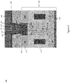
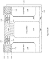
- FIG. 1 illustrates a partial cross-sectional view of a semiconductor device 100 having body contacts with dielectric spacers.
- the semiconductor device 100 includes a semiconductor substrate 102 with gate trenches 104 extending into the front surface 106 of the semiconductor substrate 102.
- the semiconductor substrate 102 can comprise any type of semiconductor material such as a single element semiconductor (e.g. Si, Ge, etc.), silicon-on-insulator, a binary semiconductor (e.g. SiC, GaN, GaAs, etc.), a ternary semiconductor, etc. with or without epitaxial layer(s).
- a gate electrode 108 and a gate dielectric 110 are disposed in each gate trench 104, the gate dielectric 110 separating the corresponding gate electrode 108 from the semiconductor substrate 102.
- a field plate 112 can be disposed in the gate trenches 104 below the gate electrodes 108, each field plate 112 being separated from the semiconductor substrate 102 and the corresponding gate electrode 108 by a field dielectric 114 that is thicker than the gate dielectric 110.
- field plates can be disposed in dedicated field plate trenches which are not shown in Figure 1 .
- a first (source/emitter) region 116 having a first conductivity type (e.g. n-type in the case of an n-channel device, or p-type in the case of a p-channel device) is formed in the semiconductor substrate 102 at the front surface 106 and adjacent each gate trench 104.
- a second (body) region 118 having a second conductivity type (e.g. p-type in the case of an n-channel device, or n-type in the case of a p-channel device) is formed in the semiconductor substrate 102 below the source/emitter region 116 and adjacent each gate trench 104.
- a third (drift) region 120 having the first conductivity type is formed in the semiconductor substrate 102, e.g.
- a drain/collector region 122 of the first conductivity type is formed at the back surface 124 of the semiconductor substrate 102 opposite the front surface 106, and is doped more heavily than the drift region 120.
- the semiconductor device 100 shown in Figure 1 is a vertical power MOSFET which has a channel region 126 that extends in the vertical direction along gate dielectric 110 in the body region 118.
- minority carriers (electrons in the case of a p-type body region 118, or holes in the case of an n-type body region 118) collect along the gate dielectric 110 in the channel region 126 and an electrically conductive path is completed between the source/emitter region 116 and the drain/collector region 122 via the drift and channel regions 120, 126.
- An interlayer dielectric 128 such a silicon dioxide, silicon nitride, tetraethoxysilane (TEOS), etc. is formed on the front surface 106 of the semiconductor substrate 102 to separate one or more overlying metal layers (not shown) from the underlying semiconductor substrate 102.
- a contact opening 130 extends through the interlayer dielectric 128 and into the semiconductor substrate 102.
- the minimum width (w1) of the contact opening 130 is larger in the interlayer dielectric 128 than the minimum width (w2) of the contact opening 130 in the semiconductor substrate 102.
- the width of the drift region 120 between adjacent gate trenches 104 is labelled w3 in Figure 1 , and which can be in the range of several hundred nanometres, e.g.
- the part of the contact opening 130 formed in the semiconductor substrate 102 is also referred to herein as a groove.
- An electrically conductive material 132 fills the contact opening 130 to form a body contact plug 134 having a stepped profile in the contact opening 130 due to the width difference described above (w1 >w2).
- the contact opening 130 extends at least into the body region 118.
- the contact opening 130 terminates within the body region 118 so that the body contact plug 134 is separated from the drift region 120 by a section of the body region 118.
- the highly-doped body contact region 136 adjoins, and is in ohmic contact with, the body contact plug 134 at the bottom of the contact opening 130.
- An electrically insulative spacer 138 is disposed on sidewalls 140 of the semiconductor substrate 102 formed by the contact opening 130.
- the electrically conductive material 132 in the contact opening 130 adjoins the electrically insulative spacer 138 on the sidewalls 140 of the semiconductor substrate 102 formed by the contact opening 130.
- the body contact plug 134 is better decoupled from the channel regions 126 by the electrically insulative spacer 138 disposed on the sidewalls 140 of the semiconductor substrate 102 formed by the contact opening 130.
- Any suitable electrically insulating material can be used for the electrically insulative spacer 140, such as oxide, nitride, carbon, TEOS, etc.
- the electrically insulative spacer 138 extends onto the front surface 106 of the semiconductor substrate 102, along sidewalls 142 of the interlayer dielectric 128 formed by the contact opening 130, and onto the surface 144 of the interlayer dielectric 128 facing away from the semiconductor substrate 102.
- the semiconductor substrate 102 can include one or more epitaxial layers such as Si epitaxial layers.
- the heavily doped drain/collector region 122 may have been fabricated from a semiconductor wafer and the body region 118 and the drift region 120 can be formed in one or more epitaxial layers grown on the heavily doped drain/collector region 122.
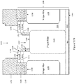
- Figure 2 illustrates a partial cross-sectional view of another embodiment of a semiconductor device 200 having a buried dielectric plug.
- the embodiment shown in Figure 2 is similar to the embodiment shown in Figure 1 .
- the portion of the electrically insulative spacer 138 disposed in the contact opening 130 is recessed below the front surface 106 of the semiconductor substrate 102 along the sidewalls 140 of the semiconductor substrate 102 formed by the contact opening 130.
- the electrically insulative spacer 138 is recessed before formation of the highly-doped body contact region 136.
- the part of the source/collector region 116 exposed as a result of the removal of the electrically insulative spacer 138 in select regions is implanted during the body contact formation process.
- a first highly-doped body contact region 136 of the second conductivity type which is doped more heavily than the body region 118, is formed in the body region 118 adjacent the bottom of the contact opening 130.
- a second highly-doped body contact region 202 of the second conductivity type can be formed in the part of the source/collector region 116 exposed as a result of the selective removal of the electrically insulative spacer 138.
- the first highly-doped body contact region 136 adjoins, and is in ohmic contact with, the body contact plug 134 at the bottom of the contact opening 130, whereas the second highly-doped body contact region 202 adjoins, and is in ohmic contact with, the body contact plug 134 along the part of the contact opening 130 devoid of the electrically insulative spacer 138.
- a variation of the embodiment shown in Figure 2 can omit the second highly-doped body contact region 202, so that the source/collector region 116 is at least partly uncovered by the electrically insulative spacer 138 along the sidewalls of the contact opening 130 and possibly along part of the front surface 106 of the semiconductor substrate 102.
- the first highly-doped body contact region 136 can be formed by implantation (e.g. p+) at the bottom of the contact opening 130. Some of the dopant species being implanted may also reach uncovered portions of the sidewalls of the contact opening 130. In a first option, uncovered portions of the source/collector region 116 are implanted and include highly-doped contact region 202 in the final product. In a second option, the implantation does not essentially affect the doping of the source/collector 116 so that the final product does not include the highly-doped contact region 202, but has an overall (net) doping concentration sufficient to function as a source/collector for the device and to make sure that good ohmic contact (e.g. n+) is maintained.
- implantation e.g. p+
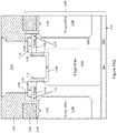
- Figure 3 illustrates a partial cross-sectional view of yet another embodiment of a semiconductor device 300 having body contacts with dielectric spacers.
- the embodiment shown in Figure 3 is similar to the embodiment shown in Figure 2 .
- a section 302 of the body region 118 extends to the front surface 106 of the semiconductor substrate 102 and each source/collector region 116 is disposed laterally between the adjacent gate trench 104 and the section 302 of the body region 118 that extends to the front surface 106 of the semiconductor substrate 102.
- the contact opening 130 is formed in the section 302 of the body region 118 that extends to the front surface 106 of the semiconductor substrate 102.
- the electrically insulative spacer 138 is recessed below the front surface 106 of the semiconductor substrate 102 along the sidewalls 140 of the section 302 of the body region 118 that extends to the front surface 106 of the semiconductor substrate 102, so that an upper part of the sidewalls 140 is devoid of the electrically insulative spacer 138.
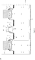
- Figure 4 illustrates a partial cross-sectional view of still another embodiment of a semiconductor device 400 having body contacts with dielectric spacers.
- the embodiment shown in Figure 4 is similar to the embodiment shown in Figure 3 .
- the contact opening 130 extends to a depth (d_co) in the semiconductor substrate 102 measured from the front surface 106 deeper than the body region 118 and into the underlying drift region 120 so that the body contact plug 134 extends into the drift region 120.
- the highly-doped body contact region 136 that adjoins the body contact plug 134 at the bottom of the contact opening 130 is formed in the drift region 118 and provides blocking capability of the resulting pn junction with the drift region 120.
- the upper highly-doped body contact region 202 provides a low-ohmic connection to the body contact plug 134 at the front surface 106 of the semiconductor substrate 102.
- the source/collector region 116 has a depth in a range between 10 nm to 50nm
- the body region 118 has a depth in a range between 100 nm and 200nm
- the interlayer dielectric 128 has a thickness in a range between 50 nm and 300 nm
- the contact opening 130 in the interlayer dielectric 128 has a minimum width w1 in a range between 200 nm and 220 nm
- the contact (groove) opening 130 in the semiconductor body 100 has a minimum width w2 in a range between 100 nm and 140 nm
- the length of the channel regions 126 in the vertical direction is in a range between 50nm and 200nm
- the lateral channel length is less than 250nm.
- Other depth, thickness, width and length ranges are contemplated.
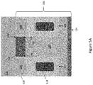
- Figures 5A through 5D illustrate an embodiment of some processing steps for manufacturing the semiconductor devices shown in Figures 1 through 4 .
- Figure 5A shows the interlayer dielectric 128 formed on the front surface 106 of the semiconductor substrate 102, after the gate trenches 104, source/collector region 116, body region 118, drift region 120, and drain/collector region 122 have been formed.
- Figure 5B shows an opening 500 formed in the interlayer dielectric 128.
- the opening 500 can be formed using a self-aligned process, using a lithography-aligned process, etc.
- the amount of overlay and critical dimension variation of the opening 130 define the width of the contact stripe to be formed.
- Figure 5C shows a groove 502 that is aligned with the opening 500 in the interlayer dielectric 128 and etched into the semiconductor body 100.
- the groove 502 extends at least into the body region 118.
- the opening 500 in the interlayer dielectric 128 and the groove 502 etched into the semiconductor body 100 form the contact opening 130.
- the groove 502 can be etched completely through the body region 118 so that the contact opening 130 extends into the underlying drift region 120 e.g. as shown in Figure 4 .
- the sidewalls 142 of the interlayer dielectric 128 formed by the opening 130 are etched back to define the thickness (t_s) of the electrically insulative spacer 138 to be formed.
- the thickness of the electrically insulative spacer 138 is in a range between 10 nm and 30 nm. In one embodiment, the width of the semiconductor fin or stripe 504 between each side of the contact opening 130 and the corresponding gate trench 104 is less than 100 nm e.g. between 80 nm and 100 nm.
- Figure 5D shows the electrically insulative spacer 138 formed on the surface 144 of the interlayer dielectric 128 facing away from the semiconductor substrate 102, on the etched-back sidewalls 142 of the interlayer dielectric 128, on the front surface 106 of the source/emitter region 116, and on the sidewalls 140 of the groove 502 formed in the semiconductor substrate 102 that extends at least into the body region 118.
- the electrically insulative spacer 138 Prior to deposition of the electrically conductive material 132 which fills the contact opening 130, the electrically insulative spacer 138 is removed from the bottom of the contact opening 130.
- the electrically insulative spacer 138 also can be removed from the front surface 106 of the source/emitter region 116 and along the upper part of the sidewalls 140 of the groove 502 formed in the semiconductor substrate 102 e.g. as shown in Figures 2 through 4 .
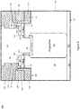
- Figure 6 illustrates a partial top plan view of the semiconductor device embodiments shown in Figures 1 through 4 .
- the top-half of Figure 6 illustrates the upper features of the semiconductor device 100 shown in Figure 1 .
- the bottom-half of Figure 6 illustrates the upper features of the semiconductor devices 200, 300, 400 shown in Figures 2 through 4 .
- the gate trenches 104 (out of view in Figure 6 ), source region 116, body region 118, and contact opening 130 are each stripe-shaped and extend in a longitudinal direction of the semiconductor substrate 102.
- the dashed line in Figure 6 demarcates the top and bottom halves of the figure.
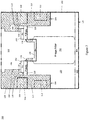
- Figure 7 illustrates a partial cross-sectional view of an embodiment of a semiconductor device 700 having body contacts with dielectric spacers.
- the embodiment shown in Figure 7 is similar to the embodiment shown in Figure 4 .
- a pillar/column/stripe region 702 of the second conductivity type is formed in the drift region 120 and adjoins the highly-doped body contact region 136 below the bottom of the contact opening 130.
- the pillar/column/stripe region 702 of the second conductivity type extends to a greater depth in the semiconductor substrate 102 as measured from the front surface 106 than the gate trenches 104 and the highly-doped body contact region 136.
- the pillar/column/stripe region 702 of the second conductivity type extends to and adjoins the drain/collector region 122 at the bottom surface 124 of the semiconductor substrate 102.
- an additional highly-doped body contact region 202 of the second conductivity type is formed on a section of the body region 118 adjacent the contact opening 130.
- the additional body contact region 202 is doped more heavily than the body region 118.
- the source/emitter region 116 adjoins a side surface 704 of the additional body contact region 202 facing the neighbouring gate trench 104, and extends onto the front surface 706 of the additional body contact region 202.
- the electrically conductive material filling the contact opening also adjoins the front surface of the additional body contact region.
- Figure 8 illustrates a partial cross-sectional view of another embodiment of a semiconductor device 800 having body contacts with dielectric spacers.
- the embodiment shown in Figure 8 is similar to the embodiment shown in Figure 7 .
- the gate trenches 104 do not include field plates.
- Figure 9 illustrates a partial cross-sectional view of yet another embodiment of a semiconductor device 900 having body contacts with dielectric spacers.
- the embodiment shown in Figure 9 is similar to the embodiment shown in Figure 7 .
- a pillar/column/stripe region 902 of the first conductivity type is formed in the drift region 120 under each gate trench 104.
- the pillar/column/stripe region 902 of the first conductivity type is laterally separated from the pillar/column/stripe region 702 of the second conductivity type by a section of the drift region 120.
- the pillar/column/stripe region 902 of the first conductivity type extends to and adjoins the drain/collector region 122 at the back surface 124 of the semiconductor substrate 102.
- the drain/collector region 122 is doped more heavily than the pillar/column/stripe region 902 of the first conductivity type.
- Figure 10 illustrates a partial cross-sectional view of still another embodiment of a semiconductor device 1000 having body contacts with dielectric spacers.
- the embodiment shown in Figure 10 is similar to the embodiment shown in Figure 8 .
- a pillar/column/stripe region 902 of the first conductivity type is formed in the drift region 120 under each gate trench 104.
- the pillar/column/stripe region 902 of the first conductivity type is laterally separated from the pillar/column/stripe region 702 of the second conductivity type by a section of the drift region 120.
- the pillar/column/stripe region 902 of the first conductivity type extends to and adjoins the drain/collector region 122 at the back surface 124 of the semiconductor substrate 102.
- the drain/collector region 122 is doped more heavily than the pillar/column/stripe region 902 of the first conductivity type.
- the semiconductor devices 700, 800, 900, 1000 illustrated in Figures 7 through 10 are shown as an n-channel devices, but the conductivity types of the device regions can be reversed to instead realize p-channel devices.
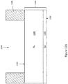
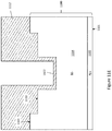
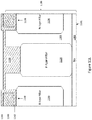
- Figures 11A through 11Q illustrate an embodiment of a method of manufacturing the semiconductor device 1000 shown in Figure 10 .
- Figure 11A shows a semiconductor substrate 1100 with an n+ region 1102 at the back surface 1101 of the substrate 1000 and a n- region 1104 adjoining the n+ region 1102.
- the semiconductor substrate 1100 can comprise any type of semiconductor material such as a single element semiconductor (e.g. Si, Ge, etc.), silicon-on-insulator, a binary semiconductor (e.g. SiC, GaN, GaAs, etc.), a ternary semiconductor, etc. with or without epitaxial layer(s).
- the n- region 1104 can be formed, e.g., as part of an epitaxial layer.
- a hard mask 1106 is formed on the front surface 1103 of the semiconductor substrate 1100.
- An opening 1108 is etched through the hard mask 1106, e.g. using an anisotropic etch process, to expose part of the front surface 1103 of the semiconductor substrate 1100.
- Figure 11B shows the semiconductor substrate 1100 after the part of the semiconductor substrate 1100 exposed by the opening 1108 in the hard mask 1106 is recessed below the front surface 1103 of the substrate 1100.
- the depth of the recess 1110 can vary based on the application.
- Figure 11C shows the semiconductor substrate 1100 after the hard mask 1106 is removed and a spacer oxide 1112 is formed on the front surface 1103 of the substrate 1100.
- An opening 1114 is etched through the spacer oxide 1112 to expose part of the recessed surface 1110 of the semiconductor substrate 1100.
- Figure 11D shows the semiconductor substrate 1100 after a groove 1116 is etched into the exposed part of the recessed surface 1110 of the semiconductor substrate 1100.
- the groove 1116 has sidewalls 1118 and a bottom 1120.
- the depth of the groove 1116 can vary depending on the application.
- Figure 11E shows the semiconductor substrate 1100 after a sacrificial oxide 1122 is formed on the sidewalls 1118 and bottom 1120 of the groove 1116 formed in the recessed surface 1110 of the semiconductor substrate 1100.
- Figure 11F shows the semiconductor substrate 1100 after a p-type pillar/column/stripe region 1124 is implanted into the n- layer 1104 through the bottom 1120 of the groove 1116 formed in the recessed surface 1110 of the semiconductor substrate 1100.
- Figure 11G shows the semiconductor substrate 1100 after the spacer oxide 1112 and the sacrificial oxide 1122 are removed and the recessed part of the substrate 1100 is filled with an oxide 1126.
- the spacer oxide 1112 and the sacrificial oxide 1122 are removed from the front surface 1103 of the semiconductor substrate 1100, e.g., by a CMP (chemical-mechanical polishing) process which stops on the semiconductor material of the substrate 1100.
- CMP chemical-mechanical polishing
- Figure 11H shows the semiconductor substrate 1100 after trenches 1128 are etched into the part of the substrate 1100 not protected by the sacrificial oxide 1126.
- Each trench 1128 has sidewalls 1130 and a bottom 1132.
- Figure 11I shows the semiconductor substrate 1100 after a sacrificial oxide 1134 is formed on the sidewalls 1130 and bottom 1132 of the trenches 1128.
- Figure 11J shows the semiconductor substrate 1100 after an n-type pillar/column/stripe region 1136 is implanted into the n- layer 1104 through the bottom 1132 of each trench 1128.
- the p-type pillar/column/stripe regions 1124 extend to the n+ layer 1102 at the back surface 1101 of the semiconductor substrate whereas the n-type pillar/column/stripe regions terminate in the n- layer before reaching the n+ layer.
- Figure 11K shows the semiconductor substrate 1100 after the sacrificial oxide 1134 is removed, a gate oxide is formed on the sidewalls 1130 and bottom 1132 of each trench 1128, and each trench 1128 is filled with an electrically conductive material such as doped polysilicon.
- the gate oxide and electrically conductive material are planarized, e.g., by a CMP (chemical-mechanical polishing) process which stops on the semiconductor material of the substrate 1100.
- the resulting trench structures form gate trenches 1138, each of which includes a gate electrode 1140 and a gate dielectric 1142 in the trench 1138, the gate dielectric 1142 separating the gate electrode 1140 from the semiconductor substrate 1100.
- Figure 11L shows the semiconductor substrate 1100 after the front surface of the substrate 1100 is recessed, e.g. by dry and/or wet etching, between the gate trenches 1138 to recess the n- layer 1104 in this region of the substrate 1100. Also, the gate electrodes 1140 are covered with an oxide 1144.
- Figure 11M shows the semiconductor substrate 1100 after p-type body regions 1146 and n-type source/emitter regions 1148 are formed in the n- layer 1104 between the gate trenches 1138.
- P-type dopants are implanted into the semiconductor substrate 1100 between the gate trenches 1138 and annealed to form the p-type body regions 1146
- n-type dopants are implanted between the gate trenches 1138 and annealed to form the source/emitter regions 1148.
- Figure 11N shows the semiconductor substrate 1100 after an interlayer dielectric 1150 is formed on the front surface of the semiconductor substrate 1100, an opening 1152 is formed in the interlayer dielectric 1150 and a groove 1154 is etched into the part of the semiconductor substrate 1100 exposed by the opening 1152 in the interlayer dielectric 1150.
- the opening 1152 in the interlayer dielectric 1150 is wider than the contact groove 1154 etched in the semiconductor substrate 1100.
- the interlayer dielectric material is removed from the part of the front face 1156 of the source/emitter regions 1148 closest to the contact groove 1154 and from the side faces 1158 of the source/emitter regions 1148 facing toward the contact groove 1154, exposing these faces 1156, 1158 of the source/emitter regions 1148.
- the interlayer dielectric material remains on the sidewalls 1160 of the contact groove 1154 below the source/emitter regions 1148 to form dielectric spacers 1151, but is removed from the bottom 1162 of the contact groove 1154.
- Figure 11O shows the semiconductor substrate 1100 after the exposed surfaces 1156, 1158 of the source/emitter regions 1148 are etched away so as to laterally recess each source/emitter region 1148 in a direction toward the neighboring gate trench 1138, thereby exposing the part of the front face 1164 of the body regions 1146 closest to contact groove 1166.
- Figure 11P shows the semiconductor substrate 1100 after p-type dopants are implanted into the exposed parts of the substrate 1100 and subsequently annealed to form a first highly-doped (e.g. p+) body contact region 1168 at the bottom of each contact groove 1166 and a second highly-doped (e.g. p+) body contact region 1170 in the exposed part of the front face 1164 of each body region 1146 closest to the corresponding contact groove 1166.
- Figure 11Q shows the semiconductor substrate 1100 after an electrically conductive material 1172 such is metal is deposited over the substrate to fill the contact openings 1166.
- the electrically conductive material adjoins the recessed part of the semiconductor substrate 1100, and is planarized e.g. by a CMP process.
- the semiconductor device regions illustrated in Figures 11A through 11Q are shown as device regions of an n-channel device, but the conductivity types of the device regions can be reversed to instead realize a p-channel device.
- the superjunction charge-balance structure formed by the p-type and n-type pillars/columns/stripes 1124, 1136 results in reduced on-resistance while maintaining required breakdown voltage.
- dielectric spacers 1151 in the body contact openings to separate the channel regions 1174 from the underlying p-type pillars/columns/stripes 1124 the width needed for the p-type pillars/columns/stripes 1124 can be reduced which in turn decreases the energy levels needed to implant the p-type pillars/columns/stripes 1124 which are used to form a superjunction structure and achieve charge balance.
- the required voltage can be sustained while also relocating the impact ionization location to the vicinity of the p-type pillars/columns/stripes.
- Such a construction causes a greater portion of avalanche current to go directly through the p-type pillars/columns/stripes and disperse to the source metal, and by doing so, effectively avoids high current density surrounding the source/emitter region and subsequent turn on the parasitic BJT which could otherwise destroy the device.
- the depth of the gate trenches 1138 can be varied to adjust gate charge and gate resistance.
- Figure 12 illustrates a partial cross-sectional view of an embodiment of a semiconductor device 1200 having body contacts with dielectric spacers.
- the embodiment shown in Figure 12 is similar to the embodiments shown in Figures 10 and 11Q .
- the semiconductor device 1200 also includes a Schottky barrier diode 1202 formed in the semiconductor substrate 102 between adjacent body contact openings/grooves 130 formed in the substrate 102.
- the Schottky barrier diode 1202 is spaced apart from each neighbouring gate trench 104 by a respective contact opening/groove 130 extending along each longitudinal side of the Schottky barrier diode 1202.
- One sidewall 1204 of the semiconductor substrate 102 formed by each adjacent contact opening/groove 130 adjoins the Schottky barrier diode 1202.
- the Schottky barrier diode 1202 includes a Schottky contact 1206 on the front face 106 of the semiconductor substrate 102 between the neighbouring contact openings/grooves 130 formed in the substrate 102. Any suitable metal or metal silicide can be used for the Schottky contact 1206.
- a guard ring 1208 of p+ semiconductor material can be provided around the edge of the Schottky barrier diode 1202, surrounding the Schottky contact 1206. The guard ring 1208 drives the adjacent semiconductor region into avalanche breakdown before the Schottky junction is damaged by large levels of reverse current flow during transient events.
- the Schottky barrier diode 1202 has low leakage, low forward voltage and when merged with a power MOSFET, low reverse recovery charge Qrr.
- Gate trenches 104 with underlying superjunction structures formed by pillar/column/stripe region 702 of the second conductivity type and the drift region 120 of the first conductivity type flank both the gate regions and the diode mesas.
- the superjunction structures underneath the body contacts 136 at the bottom of the contact openings/grooves 130 reduce leakage when the device 1200 is off at both the Schottky barrier and at the body diode of the transistor.
- the conductivity types of the device regions can be reversed in Figure 12 to realize p-channel devices instead of n-channel devices.
Landscapes
- Electrodes Of Semiconductors (AREA)
- Chemical & Material Sciences (AREA)
- Composite Materials (AREA)
Abstract
Description
- The channel dimensions of power MOSFETs are routinely reduced to increase performance. The distance between the channel and the groove contact to the body region of the device also becomes smaller, resulting in several crucial trade-offs including: the interaction of the p+ contact implant into the groove with channel dopants; and the slope of the threshold voltage characteristic decreases as parasitic source capacitance increases and gate control is reduced by depletion capacitance.
- The distance between the channel and the groove contact can be kept large enough, but this results in higher Rdson (on-state resistance). The decrease in the slope of the threshold voltage characteristic can be addressed by using thinner oxide which yields smaller gate capacitance. However, smaller gate capacitance increases gate total charge Figure of Merit (FOMg).
- Hence, new power MOSFETs with smaller channel dimensions and acceptable FOMg are needed.
- According to an embodiment of a semiconductor device, the semiconductor device comprises: a trench extending into a first main surface of a semiconductor substrate; a gate electrode and a gate dielectric in the trench, the gate dielectric separating the gate electrode from the semiconductor substrate; a first region having a first conductivity type formed in the semiconductor substrate at the first surface and adjacent the trench; a second region having a second conductivity type formed in the semiconductor substrate below the first region and adjacent the trench; a third region having the first conductivity type formed in the semiconductor substrate below the second region and adjacent the trench; a contact opening in the semiconductor substrate which extends into the second region; an electrically insulative spacer on sidewalls of the semiconductor substrate formed by the contact opening; and an electrically conductive material in the contact opening and adjoining the electrically insulative spacer on the sidewalls of the semiconductor substrate formed by the contact opening. Corresponding methods of manufacture are also provided.
- In the following, some exemplary embodiments are presented. The additional features of these exemplary embodiments can be combined with each other for forming yet further embodiments if not explicitly stated otherwise:
- In an embodiment, the electrically insulative spacer is recessed below the first main surface of the semiconductor substrate along the sidewalls of the semiconductor substrate formed by the contact opening.
- In an embodiment, the contact opening terminates within the second region so that the electrically conductive material is separated from the third region by a section of the second region.
- In an embodiment, the semiconductor device further comprises an additional region of the second conductivity type formed in the second region adjacent a bottom of the contact opening, wherein the additional region is doped more heavily than the second region and adjoins the electrically conductive material at the bottom of the contact opening.
- In an embodiment, the contact opening extends through the second region and into the third region so that the electrically conductive material extends into the third region.
- In an embodiment, the semiconductor device further comprises a first additional region of the second conductivity type formed in the third region and adjoining the electrically conductive material at a bottom of the contact opening.
- In an embodiment, the semiconductor device further comprises a second additional region of the second conductivity type formed in the third region, wherein the second additional region of the second conductivity type adjoins the first additional region of the second conductivity type below the bottom of the contact opening and extends to a greater depth in the semiconductor substrate as measured from the first main surface than both the trench and the first additional region of the second conductivity type, and wherein the first additional region of the second conductivity type is doped more heavily than the second additional region of the second conductivity type.
- In an embodiment, the semiconductor device further comprises a first additional region of the first conductivity type formed at a second main surface of the semiconductor substrate opposite the first main surface, wherein the first additional region of the first conductivity type is doped more heavily than the third region, and wherein the second additional region of the second conductivity type extends to and adjoins the first additional region of the first conductivity type.
- In an embodiment, the semiconductor device further comprises a second additional region of the first conductivity type formed in the third region under the trench, wherein the first additional region of the first conductivity type is doped more heavily than the second additional region of the first conductivity type, and wherein the second additional region of the second conductivity type is laterally separated from the second additional region of the first conductivity type by a section of the third region.
- In an embodiment, the second additional region of the first conductivity type extends to and adjoins the first additional region of the first conductivity type.
- In an embodiment, the semiconductor device further comprises a field plate in the trench below the gate electrode, wherein the field plate is electrically insulated from the gate electrode.
- In an embodiment, a section of the second region extends to the first main surface of the semiconductor substrate, wherein the first region is disposed laterally between the trench and the section of the second region that extends to the first main surface of the semiconductor substrate, and wherein the contact opening is formed in the section of the second region that extends to the first main surface of the semiconductor substrate.
- In an embodiment, the electrically insulative spacer is recessed below the first main surface of the semiconductor substrate along sidewalls of the section of the second region that extends to the first main surface of the semiconductor substrate so that an upper part of the sidewalls is devoid of the electrically insulative spacer.
- In an embodiment, the semiconductor device further comprises a first additional region of the second conductivity type formed in the second region adjacent the upper part of the sidewalls devoid of the electrically insulative spacer, wherein the first additional region of the second conductivity type is doped more heavily than the second region and adjoins the electrically conductive material along the upper part of the sidewalls devoid of the electrically insulative spacer.
- In an embodiment, the contact opening extends through the second region and into the third region so that the electrically conductive material extends into the third region.
- In an embodiment, the semiconductor device further comprises a second additional region of the second conductivity type formed in the third region, wherein the second additional region of the second conductivity type is doped more heavily than the second region and adjoins the electrically conductive material at a bottom of the contact opening.
- In an embodiment, the contact opening terminates within the second region so that the electrically conductive material is separated from the third region by a section of the second region.
- In an embodiment, the semiconductor device further comprises a second additional region of the second conductivity type formed in the second region adjacent a bottom of the contact opening, wherein the second additional region of the second conductivity type is doped more heavily than the second region and adjoins the electrically conductive material at the bottom of the contact opening.
- In an embodiment, the semiconductor device further comprises, an interlayer dielectric on the first main surface of the semiconductor substrate, wherein the contact opening extends through the interlayer dielectric and into the semiconductor substrate, and wherein a width of the contact opening is larger in the interlayer dielectric than in the semiconductor substrate so that the electrically conductive material has a stepped profile in the contact opening.
- In an embodiment, the semiconductor device further comprises an interlayer dielectric on the first main surface of the semiconductor substrate, wherein the contact opening extends through the interlayer dielectric and into the semiconductor substrate, and wherein the electrically insulative spacer extends onto the first main surface of the semiconductor substrate and along sidewalls of the interlayer dielectric formed by the contact opening.
- In an embodiment, the electrically insulative spacer extends onto the first main surface of the semiconductor substrate.
- In an embodiment, the semiconductor device further comprises an additional region of the second conductivity type formed on a section of the second region adjacent the contact opening, wherein the additional region of the second conductivity type is doped more heavily than the second region, wherein the first region adjoins a side surface of the additional region of the second conductivity type facing the trench and extends onto a front surface of the additional region of the second conductivity type, and wherein the electrically conductive material also adjoins the front surface of the additional region of the second conductivity type.
- In an embodiment, the electrically insulative spacer comprises oxide, nitride, carbon or tetraethoxysilane.
- In an embodiment, a part of the first main surface of the semiconductor substrate is recessed in a region adjacent the contact opening, and wherein the electrically conductive material adjoins the recessed part of the first main surface.
- In an embodiment, the semiconductor device further comprises a Schottky barrier diode formed in the semiconductor substrate at a side of the contact opening opposite the trench so that the Schottky barrier diode is spaced apart from the trench by the contact opening, wherein one of the sidewalls of the semiconductor substrate formed by the contact opening adjoins the Schottky barrier diode.
- In an embodiment, the semiconductor device further comprises a first additional region of the first conductivity type formed at a second main surface of the semiconductor substrate opposite the first main surface; and a first additional region of the second conductivity type formed in the third region under the contact opening and extending to the first additional region of the first conductivity type, wherein the first additional region of the first conductivity type is doped more heavily than the third region.
- In an embodiment, the semiconductor device further comprises an additional contact opening in the semiconductor substrate at a side of the Schottky barrier diode facing away from the trench; and a second additional region of the second conductivity type formed in the third region under the additional contact opening and extending to the first additional region of the first conductivity type.
- In an embodiment, the electrically insulative spacer is recessed below the first main surface of the semiconductor substrate along sidewalls of the first region, wherein the first region includes a first additional region of the second conductivity type adjacent the sidewalls of the first region, and wherein the first region forms a source or collector of the semiconductor device.
- Those skilled in the art will recognize additional features and advantages upon reading the following detailed description, and upon viewing the accompanying drawings.
- The elements of the drawings are not necessarily to scale relative to each other. Like reference numerals designate corresponding similar parts. The features of the various illustrated embodiments can be combined unless they exclude each other. Embodiments are depicted in the drawings and are detailed in the description which follows.
-
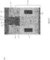
Figures 1 through 4 illustrate respective partial cross-sectional views of embodiments of semiconductor devices having body contacts with dielectric spacers. -
Figures 5A through 5D illustrate an embodiment of some processing steps for manufacturing the semiconductor devices shown inFigures 1 through 4 . -
Figure 6 illustrates a partial top plan view of the semiconductor device embodiments shown inFigures 1 through 4 . -
Figures 7 through 10 illustrate respective partial cross-sectional views of additional embodiments of semiconductor devices having body contacts with dielectric spacers. -
Figures 11A through 11Q illustrate an embodiment of a method of manufacturing the semiconductor device shown inFigure 10 . -
Figure 12 illustrates a partial cross-sectional view of an embodiment of a semiconductor device having body contacts with dielectric spacers and integrated Schottky barrier diodes. - The embodiments described herein provide power MOSFETs with reduced channel dimensions and good FOMg, and corresponding methods of manufacture. By introducing a spacer dielectric along sidewalls of the contact to the highly-doped body contact region of a power device, the lateral dimension of the channel region can be further reduced while also reducing source capacitance and increasing the distance between the highly-doped body contact region and the channel region. The small fin-like portion of the device body region between the contact opening/groove in the semiconductor substrate and the gate trench is in parallel with the contact opening/groove, reducing the swing of the IV curve and DIBL (drain-induced barrier lowering). The highly-doped body contact region is decoupled from the channel region by the spacer dielectric along the contact opening/groove, improving threshold voltage stability. The dielectric spacer also introduces stress along the channel side, which should reduce Rdson and leakage.
-
Figure 1 illustrates a partial cross-sectional view of asemiconductor device 100 having body contacts with dielectric spacers. Thesemiconductor device 100 includes asemiconductor substrate 102 withgate trenches 104 extending into thefront surface 106 of thesemiconductor substrate 102. Thesemiconductor substrate 102 can comprise any type of semiconductor material such as a single element semiconductor (e.g. Si, Ge, etc.), silicon-on-insulator, a binary semiconductor (e.g. SiC, GaN, GaAs, etc.), a ternary semiconductor, etc. with or without epitaxial layer(s). Agate electrode 108 and a gate dielectric 110 are disposed in eachgate trench 104, the gate dielectric 110 separating thecorresponding gate electrode 108 from thesemiconductor substrate 102. Afield plate 112 can be disposed in thegate trenches 104 below thegate electrodes 108, eachfield plate 112 being separated from thesemiconductor substrate 102 and thecorresponding gate electrode 108 by a field dielectric 114 that is thicker than the gate dielectric 110. Alternatively or additionally, field plates can be disposed in dedicated field plate trenches which are not shown inFigure 1 . - A first (source/emitter)
region 116 having a first conductivity type (e.g. n-type in the case of an n-channel device, or p-type in the case of a p-channel device) is formed in thesemiconductor substrate 102 at thefront surface 106 and adjacent eachgate trench 104. A second (body)region 118 having a second conductivity type (e.g. p-type in the case of an n-channel device, or n-type in the case of a p-channel device) is formed in thesemiconductor substrate 102 below the source/emitter region 116 and adjacent eachgate trench 104. A third (drift)region 120 having the first conductivity type is formed in thesemiconductor substrate 102, e.g. as part of an epitaxial layer, below thebody region 118 and adjacent eachgate trench 104. A drain/collector region 122 of the first conductivity type is formed at theback surface 124 of thesemiconductor substrate 102 opposite thefront surface 106, and is doped more heavily than thedrift region 120. - The
semiconductor device 100 shown inFigure 1 is a vertical power MOSFET which has achannel region 126 that extends in the vertical direction alonggate dielectric 110 in thebody region 118. By applying a sufficient gate voltage to thegate electrodes 108, minority carriers (electrons in the case of a p-type body region 118, or holes in the case of an n-type body region 118) collect along thegate dielectric 110 in thechannel region 126 and an electrically conductive path is completed between the source/emitter region 116 and the drain/collector region 122 via the drift andchannel regions - An
interlayer dielectric 128 such a silicon dioxide, silicon nitride, tetraethoxysilane (TEOS), etc. is formed on thefront surface 106 of thesemiconductor substrate 102 to separate one or more overlying metal layers (not shown) from theunderlying semiconductor substrate 102. Acontact opening 130 extends through theinterlayer dielectric 128 and into thesemiconductor substrate 102. In one embodiment, the minimum width (w1) of thecontact opening 130 is larger in theinterlayer dielectric 128 than the minimum width (w2) of thecontact opening 130 in thesemiconductor substrate 102. The width of thedrift region 120 betweenadjacent gate trenches 104 is labelled w3 inFigure 1 , and which can be in the range of several hundred nanometres, e.g. about 300 nm or more or less. The part of thecontact opening 130 formed in thesemiconductor substrate 102 is also referred to herein as a groove. An electricallyconductive material 132 fills thecontact opening 130 to form abody contact plug 134 having a stepped profile in thecontact opening 130 due to the width difference described above (w1 >w2). - The
contact opening 130 extends at least into thebody region 118. In the embodiment illustrated inFigure 1 , thecontact opening 130 terminates within thebody region 118 so that thebody contact plug 134 is separated from thedrift region 120 by a section of thebody region 118. A highly-doped (e.g. p+)body contact region 136 of the second conductivity type, and which is doped more heavily than thebody region 118, is formed in thebody region 118 adjacent the bottom of thecontact opening 130. The highly-dopedbody contact region 136 adjoins, and is in ohmic contact with, thebody contact plug 134 at the bottom of thecontact opening 130. - An electrically
insulative spacer 138 is disposed onsidewalls 140 of thesemiconductor substrate 102 formed by thecontact opening 130. The electricallyconductive material 132 in thecontact opening 130 adjoins the electrically insulative spacer 138 on thesidewalls 140 of thesemiconductor substrate 102 formed by thecontact opening 130. By providing the electrically insulative spacer 138 along thesidewalls 140 of thesemiconductor substrate 102 formed by thecontact opening 130, the lateral dimension of thechannel regions 126 can be reduced while also reducing source capacitance and increasing the distance between thebody contact plug 134 and thechannel regions 126. As a result, thebody contact plug 134 is better decoupled from thechannel regions 126 by the electrically insulative spacer 138 disposed on thesidewalls 140 of thesemiconductor substrate 102 formed by thecontact opening 130. Any suitable electrically insulating material can be used for the electrically insulative spacer 140, such as oxide, nitride, carbon, TEOS, etc. - According to the embodiment shown in
Figure 1 , the electrically insulative spacer 138 extends onto thefront surface 106 of thesemiconductor substrate 102, along sidewalls 142 of theinterlayer dielectric 128 formed by thecontact opening 130, and onto thesurface 144 of theinterlayer dielectric 128 facing away from thesemiconductor substrate 102. With such a contact groove spacer configuration, the ohmic contact between the highly-dopedbody contact region 136 formed in thesemiconductor substrate 102 and thebody contact plug 134 occurs only at the bottom of thecontact opening 130. As previously described herein, thesemiconductor substrate 102 can include one or more epitaxial layers such as Si epitaxial layers. For example, the heavily doped drain/collector region 122 may have been fabricated from a semiconductor wafer and thebody region 118 and thedrift region 120 can be formed in one or more epitaxial layers grown on the heavily doped drain/collector region 122. -
Figure 2 illustrates a partial cross-sectional view of another embodiment of asemiconductor device 200 having a buried dielectric plug. The embodiment shown inFigure 2 is similar to the embodiment shown inFigure 1 . Different, however, the portion of the electrically insulative spacer 138 disposed in thecontact opening 130 is recessed below thefront surface 106 of thesemiconductor substrate 102 along thesidewalls 140 of thesemiconductor substrate 102 formed by thecontact opening 130. According to this embodiment, the electrically insulative spacer 138 is recessed before formation of the highly-dopedbody contact region 136. As a result, the part of the source/collector region 116 exposed as a result of the removal of the electrically insulative spacer 138 in select regions is implanted during the body contact formation process. After a corresponding anneal process, a first highly-dopedbody contact region 136 of the second conductivity type, which is doped more heavily than thebody region 118, is formed in thebody region 118 adjacent the bottom of thecontact opening 130. A second highly-dopedbody contact region 202 of the second conductivity type can be formed in the part of the source/collector region 116 exposed as a result of the selective removal of the electrically insulative spacer 138. The first highly-dopedbody contact region 136 adjoins, and is in ohmic contact with, thebody contact plug 134 at the bottom of thecontact opening 130, whereas the second highly-dopedbody contact region 202 adjoins, and is in ohmic contact with, thebody contact plug 134 along the part of thecontact opening 130 devoid of the electrically insulative spacer 138. A variation of the embodiment shown inFigure 2 can omit the second highly-dopedbody contact region 202, so that the source/collector region 116 is at least partly uncovered by the electrically insulative spacer 138 along the sidewalls of thecontact opening 130 and possibly along part of thefront surface 106 of thesemiconductor substrate 102. For example, the first highly-dopedbody contact region 136 can be formed by implantation (e.g. p+) at the bottom of thecontact opening 130. Some of the dopant species being implanted may also reach uncovered portions of the sidewalls of thecontact opening 130. In a first option, uncovered portions of the source/collector region 116 are implanted and include highly-dopedcontact region 202 in the final product. In a second option, the implantation does not essentially affect the doping of the source/collector 116 so that the final product does not include the highly-dopedcontact region 202, but has an overall (net) doping concentration sufficient to function as a source/collector for the device and to make sure that good ohmic contact (e.g. n+) is maintained. -
Figure 3 illustrates a partial cross-sectional view of yet another embodiment of asemiconductor device 300 having body contacts with dielectric spacers. The embodiment shown inFigure 3 is similar to the embodiment shown inFigure 2 . Different, however, asection 302 of thebody region 118 extends to thefront surface 106 of thesemiconductor substrate 102 and each source/collector region 116 is disposed laterally between theadjacent gate trench 104 and thesection 302 of thebody region 118 that extends to thefront surface 106 of thesemiconductor substrate 102. Thecontact opening 130 is formed in thesection 302 of thebody region 118 that extends to thefront surface 106 of thesemiconductor substrate 102. The electrically insulative spacer 138 is recessed below thefront surface 106 of thesemiconductor substrate 102 along thesidewalls 140 of thesection 302 of thebody region 118 that extends to thefront surface 106 of thesemiconductor substrate 102, so that an upper part of thesidewalls 140 is devoid of the electrically insulative spacer 138. -
Figure 4 illustrates a partial cross-sectional view of still another embodiment of asemiconductor device 400 having body contacts with dielectric spacers. The embodiment shown inFigure 4 is similar to the embodiment shown inFigure 3 . Different, however, thecontact opening 130 extends to a depth (d_co) in thesemiconductor substrate 102 measured from thefront surface 106 deeper than thebody region 118 and into theunderlying drift region 120 so that thebody contact plug 134 extends into thedrift region 120. According to this embodiment, the highly-dopedbody contact region 136 that adjoins thebody contact plug 134 at the bottom of thecontact opening 130 is formed in thedrift region 118 and provides blocking capability of the resulting pn junction with thedrift region 120. The upper highly-dopedbody contact region 202 provides a low-ohmic connection to thebody contact plug 134 at thefront surface 106 of thesemiconductor substrate 102. - In some embodiments, the source/
collector region 116 has a depth in a range between 10 nm to 50nm, thebody region 118 has a depth in a range between 100 nm and 200nm, theinterlayer dielectric 128 has a thickness in a range between 50 nm and 300 nm, thecontact opening 130 in theinterlayer dielectric 128 has a minimum width w1 in a range between 200 nm and 220 nm, the contact (groove) opening 130 in thesemiconductor body 100 has a minimum width w2 in a range between 100 nm and 140 nm, the length of thechannel regions 126 in the vertical direction is in a range between 50nm and 200nm, and/or the lateral channel length is less than 250nm. Other depth, thickness, width and length ranges are contemplated. -
Figures 5A through 5D illustrate an embodiment of some processing steps for manufacturing the semiconductor devices shown inFigures 1 through 4 . -
Figure 5A shows theinterlayer dielectric 128 formed on thefront surface 106 of thesemiconductor substrate 102, after thegate trenches 104, source/collector region 116,body region 118, driftregion 120, and drain/collector region 122 have been formed. -
Figure 5B shows anopening 500 formed in theinterlayer dielectric 128. Theopening 500 can be formed using a self-aligned process, using a lithography-aligned process, etc. The amount of overlay and critical dimension variation of theopening 130 define the width of the contact stripe to be formed. -
Figure 5C shows agroove 502 that is aligned with theopening 500 in theinterlayer dielectric 128 and etched into thesemiconductor body 100. Thegroove 502 extends at least into thebody region 118. Theopening 500 in theinterlayer dielectric 128 and thegroove 502 etched into thesemiconductor body 100 form thecontact opening 130. Thegroove 502 can be etched completely through thebody region 118 so that thecontact opening 130 extends into theunderlying drift region 120 e.g. as shown inFigure 4 . In either case, thesidewalls 142 of theinterlayer dielectric 128 formed by theopening 130 are etched back to define the thickness (t_s) of the electrically insulative spacer 138 to be formed. In one embodiment, the thickness of the electrically insulative spacer 138 is in a range between 10 nm and 30 nm. In one embodiment, the width of the semiconductor fin orstripe 504 between each side of thecontact opening 130 and thecorresponding gate trench 104 is less than 100 nm e.g. between 80 nm and 100 nm. -
Figure 5D shows the electrically insulative spacer 138 formed on thesurface 144 of theinterlayer dielectric 128 facing away from thesemiconductor substrate 102, on the etched-backsidewalls 142 of theinterlayer dielectric 128, on thefront surface 106 of the source/emitter region 116, and on thesidewalls 140 of thegroove 502 formed in thesemiconductor substrate 102 that extends at least into thebody region 118. Prior to deposition of the electricallyconductive material 132 which fills thecontact opening 130, the electrically insulative spacer 138 is removed from the bottom of thecontact opening 130. The electrically insulative spacer 138 also can be removed from thefront surface 106 of the source/emitter region 116 and along the upper part of thesidewalls 140 of thegroove 502 formed in thesemiconductor substrate 102 e.g. as shown inFigures 2 through 4 . -
Figure 6 illustrates a partial top plan view of the semiconductor device embodiments shown inFigures 1 through 4 . The top-half ofFigure 6 illustrates the upper features of thesemiconductor device 100 shown inFigure 1 . The bottom-half ofFigure 6 illustrates the upper features of thesemiconductor devices Figures 2 through 4 . In each case, the gate trenches 104 (out of view inFigure 6 ),source region 116,body region 118, andcontact opening 130 are each stripe-shaped and extend in a longitudinal direction of thesemiconductor substrate 102. The dashed line inFigure 6 demarcates the top and bottom halves of the figure. -
Figure 7 illustrates a partial cross-sectional view of an embodiment of asemiconductor device 700 having body contacts with dielectric spacers. The embodiment shown inFigure 7 is similar to the embodiment shown inFigure 4 . Different, however, a pillar/column/stripe region 702 of the second conductivity type is formed in thedrift region 120 and adjoins the highly-dopedbody contact region 136 below the bottom of thecontact opening 130. The pillar/column/stripe region 702 of the second conductivity type extends to a greater depth in thesemiconductor substrate 102 as measured from thefront surface 106 than thegate trenches 104 and the highly-dopedbody contact region 136. In one embodiment, the pillar/column/stripe region 702 of the second conductivity type extends to and adjoins the drain/collector region 122 at thebottom surface 124 of thesemiconductor substrate 102. - Further according to the embodiment illustrated in
Figure 7 , an additional highly-dopedbody contact region 202 of the second conductivity type is formed on a section of thebody region 118 adjacent thecontact opening 130. The additionalbody contact region 202 is doped more heavily than thebody region 118. The source/emitter region 116 adjoins aside surface 704 of the additionalbody contact region 202 facing the neighbouringgate trench 104, and extends onto thefront surface 706 of the additionalbody contact region 202. The electrically conductive material filling the contact opening also adjoins the front surface of the additional body contact region. -
Figure 8 illustrates a partial cross-sectional view of another embodiment of asemiconductor device 800 having body contacts with dielectric spacers. The embodiment shown inFigure 8 is similar to the embodiment shown inFigure 7 . Different, however, thegate trenches 104 do not include field plates. -
Figure 9 illustrates a partial cross-sectional view of yet another embodiment of asemiconductor device 900 having body contacts with dielectric spacers. The embodiment shown inFigure 9 is similar to the embodiment shown inFigure 7 . Different, however, a pillar/column/stripe region 902 of the first conductivity type is formed in thedrift region 120 under eachgate trench 104. The pillar/column/stripe region 902 of the first conductivity type is laterally separated from the pillar/column/stripe region 702 of the second conductivity type by a section of thedrift region 120. The pillar/column/stripe region 902 of the first conductivity type extends to and adjoins the drain/collector region 122 at theback surface 124 of thesemiconductor substrate 102. The drain/collector region 122 is doped more heavily than the pillar/column/stripe region 902 of the first conductivity type. -
Figure 10 illustrates a partial cross-sectional view of still another embodiment of asemiconductor device 1000 having body contacts with dielectric spacers. The embodiment shown inFigure 10 is similar to the embodiment shown inFigure 8 . Different, however, a pillar/column/stripe region 902 of the first conductivity type is formed in thedrift region 120 under eachgate trench 104. The pillar/column/stripe region 902 of the first conductivity type is laterally separated from the pillar/column/stripe region 702 of the second conductivity type by a section of thedrift region 120. The pillar/column/stripe region 902 of the first conductivity type extends to and adjoins the drain/collector region 122 at theback surface 124 of thesemiconductor substrate 102. The drain/collector region 122 is doped more heavily than the pillar/column/stripe region 902 of the first conductivity type. - The
semiconductor devices Figures 7 through 10 are shown as an n-channel devices, but the conductivity types of the device regions can be reversed to instead realize p-channel devices. -
Figures 11A through 11Q illustrate an embodiment of a method of manufacturing thesemiconductor device 1000 shown inFigure 10 . -
Figure 11A shows asemiconductor substrate 1100 with ann+ region 1102 at theback surface 1101 of thesubstrate 1000 and a n-region 1104 adjoining then+ region 1102. Thesemiconductor substrate 1100 can comprise any type of semiconductor material such as a single element semiconductor (e.g. Si, Ge, etc.), silicon-on-insulator, a binary semiconductor (e.g. SiC, GaN, GaAs, etc.), a ternary semiconductor, etc. with or without epitaxial layer(s). The n-region 1104 can be formed, e.g., as part of an epitaxial layer. Ahard mask 1106 is formed on thefront surface 1103 of thesemiconductor substrate 1100. Anopening 1108 is etched through thehard mask 1106, e.g. using an anisotropic etch process, to expose part of thefront surface 1103 of thesemiconductor substrate 1100. -
Figure 11B shows thesemiconductor substrate 1100 after the part of thesemiconductor substrate 1100 exposed by theopening 1108 in thehard mask 1106 is recessed below thefront surface 1103 of thesubstrate 1100. The depth of therecess 1110 can vary based on the application. -
Figure 11C shows thesemiconductor substrate 1100 after thehard mask 1106 is removed and aspacer oxide 1112 is formed on thefront surface 1103 of thesubstrate 1100. Anopening 1114 is etched through thespacer oxide 1112 to expose part of the recessedsurface 1110 of thesemiconductor substrate 1100. -
Figure 11D shows thesemiconductor substrate 1100 after agroove 1116 is etched into the exposed part of the recessedsurface 1110 of thesemiconductor substrate 1100. Thegroove 1116 has sidewalls 1118 and a bottom 1120. The depth of thegroove 1116 can vary depending on the application. -
Figure 11E shows thesemiconductor substrate 1100 after asacrificial oxide 1122 is formed on thesidewalls 1118 and bottom 1120 of thegroove 1116 formed in the recessedsurface 1110 of thesemiconductor substrate 1100. -
Figure 11F shows thesemiconductor substrate 1100 after a p-type pillar/column/stripe region 1124 is implanted into the n-layer 1104 through thebottom 1120 of thegroove 1116 formed in the recessedsurface 1110 of thesemiconductor substrate 1100. -
Figure 11G shows thesemiconductor substrate 1100 after thespacer oxide 1112 and thesacrificial oxide 1122 are removed and the recessed part of thesubstrate 1100 is filled with anoxide 1126. Thespacer oxide 1112 and thesacrificial oxide 1122 are removed from thefront surface 1103 of thesemiconductor substrate 1100, e.g., by a CMP (chemical-mechanical polishing) process which stops on the semiconductor material of thesubstrate 1100. -
Figure 11H shows thesemiconductor substrate 1100 aftertrenches 1128 are etched into the part of thesubstrate 1100 not protected by thesacrificial oxide 1126. Eachtrench 1128 has sidewalls 1130 and a bottom 1132. -
Figure 11I shows thesemiconductor substrate 1100 after asacrificial oxide 1134 is formed on thesidewalls 1130 and bottom 1132 of thetrenches 1128. -
Figure 11J shows thesemiconductor substrate 1100 after an n-type pillar/column/stripe region 1136 is implanted into the n-layer 1104 through thebottom 1132 of eachtrench 1128. In one embodiment, the p-type pillar/column/stripe regions 1124 extend to then+ layer 1102 at theback surface 1101 of the semiconductor substrate whereas the n-type pillar/column/stripe regions terminate in the n- layer before reaching the n+ layer. -
Figure 11K shows thesemiconductor substrate 1100 after thesacrificial oxide 1134 is removed, a gate oxide is formed on thesidewalls 1130 and bottom 1132 of eachtrench 1128, and eachtrench 1128 is filled with an electrically conductive material such as doped polysilicon. The gate oxide and electrically conductive material are planarized, e.g., by a CMP (chemical-mechanical polishing) process which stops on the semiconductor material of thesubstrate 1100. The resulting trench structures formgate trenches 1138, each of which includes agate electrode 1140 and a gate dielectric 1142 in thetrench 1138, thegate dielectric 1142 separating thegate electrode 1140 from thesemiconductor substrate 1100. -
Figure 11L shows thesemiconductor substrate 1100 after the front surface of thesubstrate 1100 is recessed, e.g. by dry and/or wet etching, between thegate trenches 1138 to recess the n-layer 1104 in this region of thesubstrate 1100. Also, thegate electrodes 1140 are covered with anoxide 1144. -
Figure 11M shows thesemiconductor substrate 1100 after p-type body regions 1146 and n-type source/emitter regions 1148 are formed in the n-layer 1104 between thegate trenches 1138. P-type dopants are implanted into thesemiconductor substrate 1100 between thegate trenches 1138 and annealed to form the p-type body regions 1146, and n-type dopants are implanted between thegate trenches 1138 and annealed to form the source/emitter regions 1148. -
Figure 11N shows thesemiconductor substrate 1100 after aninterlayer dielectric 1150 is formed on the front surface of thesemiconductor substrate 1100, anopening 1152 is formed in theinterlayer dielectric 1150 and agroove 1154 is etched into the part of thesemiconductor substrate 1100 exposed by theopening 1152 in theinterlayer dielectric 1150. Theopening 1152 in theinterlayer dielectric 1150 is wider than thecontact groove 1154 etched in thesemiconductor substrate 1100. The interlayer dielectric material is removed from the part of thefront face 1156 of the source/emitter regions 1148 closest to thecontact groove 1154 and from the side faces 1158 of the source/emitter regions 1148 facing toward thecontact groove 1154, exposing thesefaces emitter regions 1148. The interlayer dielectric material remains on thesidewalls 1160 of thecontact groove 1154 below the source/emitter regions 1148 to formdielectric spacers 1151, but is removed from thebottom 1162 of thecontact groove 1154. -
Figure 11O shows thesemiconductor substrate 1100 after the exposedsurfaces emitter regions 1148 are etched away so as to laterally recess each source/emitter region 1148 in a direction toward the neighboringgate trench 1138, thereby exposing the part of thefront face 1164 of thebody regions 1146 closest to contactgroove 1166. -
Figure 11P shows thesemiconductor substrate 1100 after p-type dopants are implanted into the exposed parts of thesubstrate 1100 and subsequently annealed to form a first highly-doped (e.g. p+)body contact region 1168 at the bottom of eachcontact groove 1166 and a second highly-doped (e.g. p+)body contact region 1170 in the exposed part of thefront face 1164 of eachbody region 1146 closest to thecorresponding contact groove 1166. -
Figure 11Q shows thesemiconductor substrate 1100 after an electricallyconductive material 1172 such is metal is deposited over the substrate to fill thecontact openings 1166. The electrically conductive material adjoins the recessed part of thesemiconductor substrate 1100, and is planarized e.g. by a CMP process. The semiconductor device regions illustrated inFigures 11A through 11Q are shown as device regions of an n-channel device, but the conductivity types of the device regions can be reversed to instead realize a p-channel device. - The superjunction charge-balance structure formed by the p-type and n-type pillars/columns/
stripes dielectric spacers 1151 in the body contact openings to separate thechannel regions 1174 from the underlying p-type pillars/columns/stripes 1124, the width needed for the p-type pillars/columns/stripes 1124 can be reduced which in turn decreases the energy levels needed to implant the p-type pillars/columns/stripes 1124 which are used to form a superjunction structure and achieve charge balance. With a deep body contact opening and the contact trench with underlying p-type pillars/columns/stripes, the required voltage can be sustained while also relocating the impact ionization location to the vicinity of the p-type pillars/columns/stripes. Such a construction causes a greater portion of avalanche current to go directly through the p-type pillars/columns/stripes and disperse to the source metal, and by doing so, effectively avoids high current density surrounding the source/emitter region and subsequent turn on the parasitic BJT which could otherwise destroy the device. The depth of thegate trenches 1138 can be varied to adjust gate charge and gate resistance. -
Figure 12 illustrates a partial cross-sectional view of an embodiment of asemiconductor device 1200 having body contacts with dielectric spacers. The embodiment shown inFigure 12 is similar to the embodiments shown inFigures 10 and11Q . Different, however, thesemiconductor device 1200 also includes aSchottky barrier diode 1202 formed in thesemiconductor substrate 102 between adjacent body contact openings/grooves 130 formed in thesubstrate 102. TheSchottky barrier diode 1202 is spaced apart from each neighbouringgate trench 104 by a respective contact opening/groove 130 extending along each longitudinal side of theSchottky barrier diode 1202. Onesidewall 1204 of thesemiconductor substrate 102 formed by each adjacent contact opening/groove 130 adjoins theSchottky barrier diode 1202. TheSchottky barrier diode 1202 includes aSchottky contact 1206 on thefront face 106 of thesemiconductor substrate 102 between the neighbouring contact openings/grooves 130 formed in thesubstrate 102. Any suitable metal or metal silicide can be used for theSchottky contact 1206. Aguard ring 1208 of p+ semiconductor material can be provided around the edge of theSchottky barrier diode 1202, surrounding theSchottky contact 1206. Theguard ring 1208 drives the adjacent semiconductor region into avalanche breakdown before the Schottky junction is damaged by large levels of reverse current flow during transient events. - The
Schottky barrier diode 1202 has low leakage, low forward voltage and when merged with a power MOSFET, low reverse recovery charge Qrr.Gate trenches 104 with underlying superjunction structures formed by pillar/column/stripe region 702 of the second conductivity type and thedrift region 120 of the first conductivity type flank both the gate regions and the diode mesas. The superjunction structures underneath thebody contacts 136 at the bottom of the contact openings/grooves 130 reduce leakage when thedevice 1200 is off at both the Schottky barrier and at the body diode of the transistor. The conductivity types of the device regions can be reversed inFigure 12 to realize p-channel devices instead of n-channel devices. - Spatially relative terms such as "under", "below", "lower", "over", "upper" and the like, are used for ease of description to explain the positioning of one element relative to a second element. These terms are intended to encompass different orientations of the device in addition to different orientations than those depicted in the figures. Further, terms such as "first", "second", and the like, are also used to describe various elements, regions, sections, etc. and are also not intended to be limiting. Like terms refer to like elements throughout the description.
- As used herein, the terms "having", "containing", "including", "comprising" and the like are open-ended terms that indicate the presence of stated elements or features, but do not preclude additional elements or features. The articles "a", "an" and "the" are intended to include the plural as well as the singular, unless the context clearly indicates otherwise.
- With the above range of variations and applications in mind, it should be understood that the present invention is not limited by the foregoing description, nor is it limited by the accompanying drawings. Instead, the present invention is limited only by the following claims and their legal equivalents.
Claims (15)
- A semiconductor device, comprising:a trench extending into a first main surface of a semiconductor substrate;a gate electrode and a gate dielectric in the trench, the gate dielectric separating the gate electrode from the semiconductor substrate;a first region having a first conductivity type formed in the semiconductor substrate at the first surface and adjacent the trench;a second region having a second conductivity type formed in the semiconductor substrate below the first region and adjacent the trench;a third region having the first conductivity type formed in the semiconductor substrate below the second region and adjacent the trench;a contact opening in the semiconductor substrate which extends into the second region;an electrically insulative spacer on sidewalls of the semiconductor substrate formed by the contact opening; andan electrically conductive material in the contact opening and adjoining the electrically insulative spacer on the sidewalls of the semiconductor substrate formed by the contact opening.
- The semiconductor device of claim 1, wherein the electrically insulative spacer is recessed below the first main surface of the semiconductor substrate along the sidewalls of the semiconductor substrate formed by the contact opening.
- The semiconductor device of claim 1 or 2, wherein the contact opening terminates within the second region so that the electrically conductive material is separated from the third region by a section of the second region.
- The semiconductor device of claim 3, further comprising an additional region of the second conductivity type formed in the second region adjacent a bottom of the contact opening, wherein the additional region is doped more heavily than the second region and adjoins the electrically conductive material at the bottom of the contact opening.
- The semiconductor device of one of the preceding claims, wherein the contact opening extends through the second region and into the third region so that the electrically conductive material extends into the third region, wherein, optionally:- the semiconductor device further comprises a first additional region of the second conductivity type formed in the third region and adjoining the electrically conductive material at a bottom of the contact opening, wherein, optionally,- the semiconductor device further comprises a second additional region of the second conductivity type formed in the third region, wherein the second additional region of the second conductivity type adjoins the first additional region of the second conductivity type below the bottom of the contact opening and extends to a greater depth in the semiconductor substrate as measured from the first main surface than both the trench and the first additional region of the second conductivity type, and wherein the first additional region of the second conductivity type is doped more heavily than the second additional region of the second conductivity type, wherein, optionally,- the semiconductor device further comprises a first additional region of the first conductivity type formed at a second main surface of the semiconductor substrate opposite the first main surface, wherein the first additional region of the first conductivity type is doped more heavily than the third region, and wherein the second additional region of the second conductivity type extends to and adjoins the first additional region of the first conductivity type, wherein, optionally,- the semiconductor device further comprises a second additional region of the first conductivity type formed in the third region under the trench, wherein the first additional region of the first conductivity type is doped more heavily than the second additional region of the first conductivity type, and wherein the second additional region of the second conductivity type is laterally separated from the second additional region of the first conductivity type by a section of the third region, wherein, optionally- the second additional region of the first conductivity type extends to and adjoins the first additional region of the first conductivity type, wherein, optionally- the semiconductor device further comprises a field plate in the trench below the gate electrode, wherein the field plate is electrically insulated from the gate electrode.
- The semiconductor device of one of the preceding claims, wherein a section of the second region extends to the first main surface of the semiconductor substrate, wherein the first region is disposed laterally between the trench and the section of the second region that extends to the first main surface of the semiconductor substrate, and wherein the contact opening is formed in the section of the second region that extends to the first main surface of the semiconductor substrate.
- The semiconductor device of claim 6, wherein the electrically insulative spacer is recessed below the first main surface of the semiconductor substrate along sidewalls of the section of the second region that extends to the first main surface of the semiconductor substrate so that an upper part of the sidewalls is devoid of the electrically insulative spacer.
- The semiconductor device of claim 7, further comprising a first additional region of the second conductivity type formed in the second region adjacent the upper part of the sidewalls devoid of the electrically insulative spacer, wherein the first additional region of the second conductivity type is doped more heavily than the second region and adjoins the electrically conductive material along the upper part of the sidewalls devoid of the electrically insulative spacer.
- The semiconductor device of claim 8, wherein the contact opening extends through the second region and into the third region so that the electrically conductive material extends into the third region, wherein, optionally, the semiconductor device further comprises a second additional region of the second conductivity type formed in the third region, wherein the second additional region of the second conductivity type is doped more heavily than the second region and adjoins the electrically conductive material at a bottom of the contact opening.
- The semiconductor device of one of the preceding claims, further comprising an interlayer dielectric on the first main surface of the semiconductor substrate, wherein the contact opening extends through the interlayer dielectric and into the semiconductor substrate, and wherein a width of the contact opening is larger in the interlayer dielectric than in the semiconductor substrate so that the electrically conductive material has a stepped profile in the contact opening.
- The semiconductor device of one of the preceding claims, further comprising an interlayer dielectric on the first main surface of the semiconductor substrate, wherein the contact opening extends through the interlayer dielectric and into the semiconductor substrate, and wherein the electrically insulative spacer extends onto the first main surface of the semiconductor substrate and along sidewalls of the interlayer dielectric formed by the contact opening.
- The semiconductor device of one of the preceding claims, wherein the electrically insulative spacer extends onto the first main surface of the semiconductor substrate.
- The semiconductor device of one of the preceding claims, further comprising an additional region of the second conductivity type formed on a section of the second region adjacent the contact opening, wherein the additional region of the second conductivity type is doped more heavily than the second region, wherein the first region adjoins a side surface of the additional region of the second conductivity type facing the trench and extends onto a front surface of the additional region of the second conductivity type, and wherein the electrically conductive material also adjoins the front surface of the additional region of the second conductivity type.
- The semiconductor device of one of the preceding claims, wherein a part of the first main surface of the semiconductor substrate is recessed in a region adjacent the contact opening, and wherein the electrically conductive material adjoins the recessed part of the first main surface.
- The semiconductor device of one of the preceding claims, further comprising a Schottky barrier diode formed in the semiconductor substrate at a side of the contact opening opposite the trench so that the Schottky barrier diode is spaced apart from the trench by the contact opening, wherein one of the sidewalls of the semiconductor substrate formed by the contact opening adjoins the Schottky barrier diode
wherein, optionally,
the semiconductor device further comprises:a first additional region of the first conductivity type formed at a second main surface of the semiconductor substrate opposite the first main surface; anda first additional region of the second conductivity type formed in the third region under the contact opening and extending to the first additional region of the first conductivity type,wherein the first additional region of the first conductivity type is doped more heavily than the third region,wherein, optionally,
the semiconductor device further comprises:an additional contact opening in the semiconductor substrate at a side of the Schottky barrier diode facing away from the trench; anda second additional region of the second conductivity type formed in the third region under the additional contact opening and extending to the first additional region of the first conductivity type.
Applications Claiming Priority (1)
| Application Number | Priority Date | Filing Date | Title |
|---|---|---|---|
| US15/878,183 US11031478B2 (en) | 2018-01-23 | 2018-01-23 | Semiconductor device having body contacts with dielectric spacers and corresponding methods of manufacture |
Publications (2)
| Publication Number | Publication Date |
|---|---|
| EP3514834A1 true EP3514834A1 (en) | 2019-07-24 |
| EP3514834B1 EP3514834B1 (en) | 2025-11-05 |
Family
ID=65199352
Family Applications (1)
| Application Number | Title | Priority Date | Filing Date |
|---|---|---|---|
| EP19152974.2A Active EP3514834B1 (en) | 2018-01-23 | 2019-01-22 | Semiconductor device having body contacts with dielectric spacers and corresponding methods of manufacture |
Country Status (3)
| Country | Link |
|---|---|
| US (3) | US11031478B2 (en) |
| EP (1) | EP3514834B1 (en) |
| CN (1) | CN110071169B (en) |
Cited By (3)
| Publication number | Priority date | Publication date | Assignee | Title |
|---|---|---|---|---|
| CN115207128A (en) * | 2022-09-09 | 2022-10-18 | 深圳芯能半导体技术有限公司 | Negative-pressure-resistant silicon carbide MOSFET (Metal-oxide-semiconductor field Effect transistor) with trench side wall gate and preparation method thereof |
| CN115207130A (en) * | 2022-09-09 | 2022-10-18 | 深圳芯能半导体技术有限公司 | Side wall gate double-groove silicon carbide MOSFET and preparation method thereof |
| EP4160692A1 (en) * | 2021-09-29 | 2023-04-05 | Infineon Technologies Austria AG | Transistor device |
Families Citing this family (7)
| Publication number | Priority date | Publication date | Assignee | Title |
|---|---|---|---|---|
| US10950494B2 (en) * | 2018-01-19 | 2021-03-16 | Infineon Technologies Ag | Semiconductor device including first and second contact layers and manufacturing method |
| US11031478B2 (en) * | 2018-01-23 | 2021-06-08 | Infineon Technologies Austria Ag | Semiconductor device having body contacts with dielectric spacers and corresponding methods of manufacture |
| CN112086511B (en) * | 2019-06-13 | 2025-07-18 | 半导体元件工业有限责任公司 | System and method for self-aligned trench MOSFET contacts |
| JP7370781B2 (en) * | 2019-09-24 | 2023-10-30 | 株式会社東芝 | semiconductor equipment |
| DE102019133030B4 (en) * | 2019-12-04 | 2023-05-04 | Infineon Technologies Austria Ag | INSULATED GATE BIPOLAR TRANSISTOR INCLUDING SEMICONDUCTOR DEVICE AND METHOD OF MANUFACTURE |
| CN112164718A (en) * | 2020-08-28 | 2021-01-01 | 电子科技大学 | Split gate device with control gate protection layer and method of manufacturing the same |
| CN114823310A (en) * | 2021-01-19 | 2022-07-29 | 长鑫存储技术有限公司 | Memory device, semiconductor structure and forming method thereof |
Citations (10)
| Publication number | Priority date | Publication date | Assignee | Title |
|---|---|---|---|---|
| US20070013000A1 (en) * | 2005-07-12 | 2007-01-18 | Masaki Shiraishi | Semiconductor device and manufacturing method of the same, and non-isolated DC/DC converter |
| EP1755168A2 (en) * | 2005-08-15 | 2007-02-21 | International Rectifier Corporation | Deep N diffusion for trench IGBT |
| US20070114599A1 (en) * | 2005-11-23 | 2007-05-24 | M-Mos Sdn. Bhd. | High density trench MOSFET with reduced on-resistance |
| US20080135929A1 (en) * | 2006-11-01 | 2008-06-12 | Kabushiki Kaisha Toshiba | Power semiconductor device |
| US20090057757A1 (en) * | 2007-08-31 | 2009-03-05 | Kabushiki Kaisha Toshiba | Trench gate semiconductor device and method of manufacturing the same |
| WO2009079465A1 (en) * | 2007-12-14 | 2009-06-25 | Fairchild Semiconductor Corporation | Structure and method for forming power devices with high aspect ratio contact openings |
| US20090256197A1 (en) * | 2008-04-09 | 2009-10-15 | Yoshito Nakazawa | Semiconductor device and manufacturing method thereof |
| US20120313161A1 (en) * | 2011-06-13 | 2012-12-13 | Grivna Gordon M | Semiconductor device with enhanced mobility and method |
| US20150053999A1 (en) * | 2013-08-23 | 2015-02-26 | Fuji Electric Co., Ltd. | Wide bandgap insulated gate semiconductor device |
| US20180012956A1 (en) * | 2016-07-06 | 2018-01-11 | Kabushiki Kaisha Toshiba | Semiconductor device and method for manufacturing the same |
Family Cites Families (51)
| Publication number | Priority date | Publication date | Assignee | Title |
|---|---|---|---|---|
| CN1019720B (en) | 1991-03-19 | 1992-12-30 | 电子科技大学 | Power semiconductor device |
| US6316807B1 (en) * | 1997-12-05 | 2001-11-13 | Naoto Fujishima | Low on-resistance trench lateral MISFET with better switching characteristics and method for manufacturing same |
| GB0003185D0 (en) | 2000-02-12 | 2000-04-05 | Koninkl Philips Electronics Nv | An insulated gate field effect device |
| DE10214175B4 (en) * | 2002-03-28 | 2006-06-29 | Infineon Technologies Ag | By field effect controllable semiconductor device and method for its production |
| GB0212564D0 (en) | 2002-05-31 | 2002-07-10 | Koninkl Philips Electronics Nv | Trench-gate semiconductor device |
| AU2003260899A1 (en) | 2002-10-04 | 2004-04-23 | Koninklijke Philips Electronics N.V. | Power semiconductor devices |
| US7851349B2 (en) * | 2005-09-26 | 2010-12-14 | Infineon Technologies Austria Ag | Method for producing a connection electrode for two semiconductor zones arranged one above another |
| DE102005052734B4 (en) | 2005-10-06 | 2012-02-23 | Infineon Technologies Ag | Semiconductor structure, method for operating a semiconductor structure and method for producing a semiconductor structure |
| JP5034461B2 (en) * | 2006-01-10 | 2012-09-26 | 株式会社デンソー | Semiconductor device |
| US8618601B2 (en) * | 2009-08-14 | 2013-12-31 | Alpha And Omega Semiconductor Incorporated | Shielded gate trench MOSFET with increased source-metal contact |
| US20080272429A1 (en) * | 2007-05-04 | 2008-11-06 | Icemos Technology Corporation | Superjunction devices having narrow surface layout of terminal structures and methods of manufacturing the devices |
| JP2010541212A (en) * | 2007-09-21 | 2010-12-24 | フェアチャイルド・セミコンダクター・コーポレーション | Superjunction structure and manufacturing method for power device |
| JP5196980B2 (en) * | 2007-12-10 | 2013-05-15 | 株式会社東芝 | Semiconductor device |
| US20100013009A1 (en) * | 2007-12-14 | 2010-01-21 | James Pan | Structure and Method for Forming Trench Gate Transistors with Low Gate Resistance |
| US8253194B2 (en) * | 2008-09-17 | 2012-08-28 | Fairchild Semiconductor Corporation | Structures for reducing dopant out-diffusion from implant regions in power devices |
| US8022474B2 (en) * | 2008-09-30 | 2011-09-20 | Infineon Technologies Austria Ag | Semiconductor device |
| US20100264488A1 (en) * | 2009-04-15 | 2010-10-21 | Force Mos Technology Co. Ltd. | Low Qgd trench MOSFET integrated with schottky rectifier |
| DE102009021485B4 (en) | 2009-05-15 | 2017-10-05 | Globalfoundries Dresden Module One Llc & Co. Kg | Semiconductor device having a metal gate and a silicon-containing resistor formed on an insulating structure and method for its production |
| US8021947B2 (en) * | 2009-12-09 | 2011-09-20 | Semiconductor Components Industries, Llc | Method of forming an insulated gate field effect transistor device having a shield electrode structure |
| JP2011142269A (en) * | 2010-01-08 | 2011-07-21 | Toshiba Corp | Manufacturing method of semiconductor device and semiconductor device |
| WO2011133481A2 (en) * | 2010-04-20 | 2011-10-27 | Maxpower Semiconductor Inc. | Power mosfet with embedded recessed field plate and methods of fabrication |
| US20120037983A1 (en) * | 2010-08-10 | 2012-02-16 | Force Mos Technology Co., Ltd. | Trench mosfet with integrated schottky rectifier in same cell |
| US20120175699A1 (en) * | 2011-01-06 | 2012-07-12 | Force Mos Technology Co., Ltd. | Trench mosfet with super pinch-off regions and self-aligned trenched contact |
| US8362550B2 (en) | 2011-01-20 | 2013-01-29 | Fairchild Semiconductor Corporation | Trench power MOSFET with reduced on-resistance |
| CN102623501B (en) * | 2011-01-28 | 2015-06-03 | 万国半导体股份有限公司 | Shielded gate trench MOSFET with increased source-metal contact |
| KR101904991B1 (en) * | 2011-05-25 | 2018-10-08 | 페어차일드코리아반도체 주식회사 | Semiconductor device with super junction and method of manufacturing the same |
| US8680607B2 (en) * | 2011-06-20 | 2014-03-25 | Maxpower Semiconductor, Inc. | Trench gated power device with multiple trench width and its fabrication process |
| EP2602829A1 (en) | 2011-12-07 | 2013-06-12 | Nxp B.V. | Trench-gate resurf semiconductor device and manufacturing method |
| JP2013125827A (en) | 2011-12-14 | 2013-06-24 | Toshiba Corp | Semiconductor device and method of manufacturing the same |
| KR101876573B1 (en) * | 2011-12-23 | 2018-07-10 | 매그나칩 반도체 유한회사 | Semiconductor device and method for thereof |
| US20130256786A1 (en) * | 2012-03-29 | 2013-10-03 | Feei Cherng Enterprise Co., Ltd. | Trench mosfet with shielded electrode and avalanche enhancement region |
| US8946814B2 (en) * | 2012-04-05 | 2015-02-03 | Icemos Technology Ltd. | Superjunction devices having narrow surface layout of terminal structures, buried contact regions and trench gates |
| US9029215B2 (en) * | 2012-05-14 | 2015-05-12 | Semiconductor Components Industries, Llc | Method of making an insulated gate semiconductor device having a shield electrode structure |
| US8723317B2 (en) * | 2012-09-14 | 2014-05-13 | Force Mos Technology Co., Ltd. | Trench metal oxide semiconductor field effect transistor with embedded schottky rectifier using reduced masks process |
| US9105713B2 (en) * | 2012-11-09 | 2015-08-11 | Infineon Technologies Austria Ag | Semiconductor device with metal-filled groove in polysilicon gate electrode |
| US10629723B2 (en) * | 2012-12-28 | 2020-04-21 | Texas Instruments Incorporated | Schottky power MOSFET |
| JP6161903B2 (en) * | 2013-01-21 | 2017-07-12 | ルネサスエレクトロニクス株式会社 | Method for manufacturing power MOSFET |
| US20140291753A1 (en) * | 2013-03-27 | 2014-10-02 | Force Mos Technology Co., Ltd. | Trench mosfet structure having self-aligned features for mask saving and on-resistance reduction |
| KR101795828B1 (en) * | 2013-09-17 | 2017-11-10 | 매그나칩 반도체 유한회사 | Super-junction semiconductor device and manufacturing method thereof |
| US9324823B2 (en) | 2014-08-15 | 2016-04-26 | Infineon Technologies Austria Ag | Semiconductor device having a tapered gate structure and method |
| DE102014112371B4 (en) | 2014-08-28 | 2023-11-23 | Infineon Technologies Austria Ag | SEMICONDUCTOR DEVICE AND ELECTRONIC ARRANGEMENT COMPRISING A SEMICONDUCTOR DEVICE |
| US9722036B2 (en) | 2014-09-17 | 2017-08-01 | Infineon Technologies Austria Ag | Semiconductor device with field electrode structure |
| KR102250583B1 (en) | 2014-12-16 | 2021-05-12 | 에스케이하이닉스 주식회사 | Semiconductor device having dual work function gate structure and method for manufacturing the same, memory cell having the same and electronic device having the same |
| DE102016102493B3 (en) * | 2016-02-12 | 2017-07-20 | Infineon Technologies Ag | SEMICONDUCTOR DEVICE WITH A TEMPERATURE SENSOR, TEMPERATURE SENSOR AND METHOD FOR PRODUCING A SEMICONDUCTOR DEVICE WITH A TEMPERATURE SENSOR |
| US9953969B2 (en) * | 2016-03-25 | 2018-04-24 | Force Mos Technology Co., Ltd. | Semiconductor power device having shielded gate structure and ESD clamp diode manufactured with less mask process |
| DE102016114229B3 (en) | 2016-08-01 | 2017-12-07 | Infineon Technologies Austria Ag | TRANSISTOR COMPONENT COMPRISING A FIELD ELECTRODE COMPRISING TWO LAYERS AND ITS MANUFACTURING METHOD |
| JP2018046251A (en) * | 2016-09-16 | 2018-03-22 | 株式会社東芝 | Semiconductor device and manufacturing method thereof |
| US20190081147A1 (en) * | 2017-09-13 | 2019-03-14 | Polar Semiconductor, Llc | Mosfet with vertical variation of gate-pillar separation |
| US11031478B2 (en) * | 2018-01-23 | 2021-06-08 | Infineon Technologies Austria Ag | Semiconductor device having body contacts with dielectric spacers and corresponding methods of manufacture |
| US10861965B2 (en) * | 2018-07-12 | 2020-12-08 | Renesas Electronics America Inc. | Power MOSFET with an integrated pseudo-Schottky diode in source contact trench |
| US20220045184A1 (en) * | 2019-10-02 | 2022-02-10 | Nami MOS CO., LTD. | Shielded gate trench mosfet with esd diode manufactured using two poly-silicon layers process |
-
2018
- 2018-01-23 US US15/878,183 patent/US11031478B2/en active Active
-
2019
- 2019-01-22 EP EP19152974.2A patent/EP3514834B1/en active Active
- 2019-01-23 CN CN201910062909.2A patent/CN110071169B/en active Active
-
2021
- 2021-05-17 US US17/321,695 patent/US20210273067A1/en not_active Abandoned
-
2024
- 2024-02-16 US US18/443,354 patent/US20240194754A1/en active Pending
Patent Citations (10)
| Publication number | Priority date | Publication date | Assignee | Title |
|---|---|---|---|---|
| US20070013000A1 (en) * | 2005-07-12 | 2007-01-18 | Masaki Shiraishi | Semiconductor device and manufacturing method of the same, and non-isolated DC/DC converter |
| EP1755168A2 (en) * | 2005-08-15 | 2007-02-21 | International Rectifier Corporation | Deep N diffusion for trench IGBT |
| US20070114599A1 (en) * | 2005-11-23 | 2007-05-24 | M-Mos Sdn. Bhd. | High density trench MOSFET with reduced on-resistance |
| US20080135929A1 (en) * | 2006-11-01 | 2008-06-12 | Kabushiki Kaisha Toshiba | Power semiconductor device |
| US20090057757A1 (en) * | 2007-08-31 | 2009-03-05 | Kabushiki Kaisha Toshiba | Trench gate semiconductor device and method of manufacturing the same |
| WO2009079465A1 (en) * | 2007-12-14 | 2009-06-25 | Fairchild Semiconductor Corporation | Structure and method for forming power devices with high aspect ratio contact openings |
| US20090256197A1 (en) * | 2008-04-09 | 2009-10-15 | Yoshito Nakazawa | Semiconductor device and manufacturing method thereof |
| US20120313161A1 (en) * | 2011-06-13 | 2012-12-13 | Grivna Gordon M | Semiconductor device with enhanced mobility and method |
| US20150053999A1 (en) * | 2013-08-23 | 2015-02-26 | Fuji Electric Co., Ltd. | Wide bandgap insulated gate semiconductor device |
| US20180012956A1 (en) * | 2016-07-06 | 2018-01-11 | Kabushiki Kaisha Toshiba | Semiconductor device and method for manufacturing the same |
Cited By (4)
| Publication number | Priority date | Publication date | Assignee | Title |
|---|---|---|---|---|
| EP4160692A1 (en) * | 2021-09-29 | 2023-04-05 | Infineon Technologies Austria AG | Transistor device |
| US12453139B2 (en) | 2021-09-29 | 2025-10-21 | Infineon Technologies Austria Ag | Transistor device and method for producing a transistor device |
| CN115207128A (en) * | 2022-09-09 | 2022-10-18 | 深圳芯能半导体技术有限公司 | Negative-pressure-resistant silicon carbide MOSFET (Metal-oxide-semiconductor field Effect transistor) with trench side wall gate and preparation method thereof |
| CN115207130A (en) * | 2022-09-09 | 2022-10-18 | 深圳芯能半导体技术有限公司 | Side wall gate double-groove silicon carbide MOSFET and preparation method thereof |
Also Published As
| Publication number | Publication date |
|---|---|
| CN110071169B (en) | 2025-02-28 |
| US11031478B2 (en) | 2021-06-08 |
| EP3514834B1 (en) | 2025-11-05 |
| US20210273067A1 (en) | 2021-09-02 |
| US20240194754A1 (en) | 2024-06-13 |
| CN110071169A (en) | 2019-07-30 |
| US20190229198A1 (en) | 2019-07-25 |
Similar Documents
| Publication | Publication Date | Title |
|---|---|---|
| US20240194754A1 (en) | Semiconductor device and corresponding methods of manufacture | |
| US11538911B2 (en) | Shielded trench devices | |
| US7323386B2 (en) | Method of fabricating semiconductor device containing dielectrically isolated PN junction for enhanced breakdown characteristics | |
| US8373208B2 (en) | Lateral super junction device with high substrate-gate breakdown and built-in avalanche clamp diode | |
| US7943993B2 (en) | Structure and method for forming field effect transistor with low resistance channel region | |
| US20190348510A1 (en) | Shielded trench devices | |
| KR101404906B1 (en) | A horizontal power device comprising a self-bias electrode | |
| US11038037B2 (en) | Sawtooh electric field drift region structure for planar and trench power semiconductor devices | |
| US8519476B2 (en) | Method of forming a self-aligned charge balanced power DMOS | |
| US12464747B2 (en) | Shielded trench devices | |
| US20080017897A1 (en) | Semiconductor device and method of manufacturing same | |
| US7902601B2 (en) | Semiconductor device having deep trench charge compensation regions and method | |
| KR102723239B1 (en) | Oxygen inserted si-layers for reduced contact implant outdiffusion in vertical power devices | |
| US10186573B2 (en) | Lateral power MOSFET with non-horizontal RESURF structure | |
| US20150041946A1 (en) | Edge Termination Structure with Trench Isolation Regions | |
| KR102831136B1 (en) | Semicondector device and manufacturing method thereof |
Legal Events
| Date | Code | Title | Description |
|---|---|---|---|
| PUAI | Public reference made under article 153(3) epc to a published international application that has entered the european phase |
Free format text: ORIGINAL CODE: 0009012 |
|
| STAA | Information on the status of an ep patent application or granted ep patent |
Free format text: STATUS: THE APPLICATION HAS BEEN PUBLISHED |
|
| AK | Designated contracting states |
Kind code of ref document: A1 Designated state(s): AL AT BE BG CH CY CZ DE DK EE ES FI FR GB GR HR HU IE IS IT LI LT LU LV MC MK MT NL NO PL PT RO RS SE SI SK SM TR |
|
| AX | Request for extension of the european patent |
Extension state: BA ME |
|
| STAA | Information on the status of an ep patent application or granted ep patent |
Free format text: STATUS: REQUEST FOR EXAMINATION WAS MADE |
|
| 17P | Request for examination filed |
Effective date: 20200116 |
|
| RBV | Designated contracting states (corrected) |
Designated state(s): AL AT BE BG CH CY CZ DE DK EE ES FI FR GB GR HR HU IE IS IT LI LT LU LV MC MK MT NL NO PL PT RO RS SE SI SK SM TR |
|
| STAA | Information on the status of an ep patent application or granted ep patent |
Free format text: STATUS: EXAMINATION IS IN PROGRESS |
|
| 17Q | First examination report despatched |
Effective date: 20210805 |
|
| REG | Reference to a national code |
Ref country code: DE Free format text: PREVIOUS MAIN CLASS: H01L0029417000 Ipc: H10D0030010000 Ref country code: DE Ref legal event code: R079 Ref document number: 602019077652 Country of ref document: DE Free format text: PREVIOUS MAIN CLASS: H01L0029417000 Ipc: H10D0030010000 |
|
| GRAP | Despatch of communication of intention to grant a patent |
Free format text: ORIGINAL CODE: EPIDOSNIGR1 |
|
| STAA | Information on the status of an ep patent application or granted ep patent |
Free format text: STATUS: GRANT OF PATENT IS INTENDED |
|
| RIC1 | Information provided on ipc code assigned before grant |
Ipc: H10D 30/01 20250101AFI20250627BHEP Ipc: H10D 30/66 20250101ALI20250627BHEP Ipc: H10D 62/10 20250101ALI20250627BHEP Ipc: H10D 62/13 20250101ALI20250627BHEP Ipc: H10D 62/17 20250101ALI20250627BHEP Ipc: H10D 64/00 20250101ALI20250627BHEP Ipc: H10D 64/23 20250101ALI20250627BHEP Ipc: H10D 30/69 20250101ALI20250627BHEP Ipc: H10D 84/00 20250101ALI20250627BHEP |
|
| INTG | Intention to grant announced |
Effective date: 20250709 |
|
| GRAS | Grant fee paid |
Free format text: ORIGINAL CODE: EPIDOSNIGR3 |
|
| GRAA | (expected) grant |
Free format text: ORIGINAL CODE: 0009210 |
|
| STAA | Information on the status of an ep patent application or granted ep patent |
Free format text: STATUS: THE PATENT HAS BEEN GRANTED |
|
| AK | Designated contracting states |
Kind code of ref document: B1 Designated state(s): AL AT BE BG CH CY CZ DE DK EE ES FI FR GB GR HR HU IE IS IT LI LT LU LV MC MK MT NL NO PL PT RO RS SE SI SK SM TR |
|
| REG | Reference to a national code |
Ref country code: CH Ref legal event code: F10 Free format text: ST27 STATUS EVENT CODE: U-0-0-F10-F00 (AS PROVIDED BY THE NATIONAL OFFICE) Effective date: 20251105 Ref country code: GB Ref legal event code: FG4D |
|
| REG | Reference to a national code |
Ref country code: DE Ref legal event code: R096 Ref document number: 602019077652 Country of ref document: DE |
|
| REG | Reference to a national code |
Ref country code: IE Ref legal event code: FG4D |
|
| P01 | Opt-out of the competence of the unified patent court (upc) registered |
Free format text: CASE NUMBER: UPC_APP_0001756_3514834/2026 Effective date: 20260119 |
|
| REG | Reference to a national code |
Ref country code: NL Ref legal event code: MP Effective date: 20251105 |
|
| PG25 | Lapsed in a contracting state [announced via postgrant information from national office to epo] |
Ref country code: ES Free format text: LAPSE BECAUSE OF FAILURE TO SUBMIT A TRANSLATION OF THE DESCRIPTION OR TO PAY THE FEE WITHIN THE PRESCRIBED TIME-LIMIT Effective date: 20251105 |
|
| REG | Reference to a national code |
Ref country code: LT Ref legal event code: MG9D |
|
| PG25 | Lapsed in a contracting state [announced via postgrant information from national office to epo] |
Ref country code: NO Free format text: LAPSE BECAUSE OF FAILURE TO SUBMIT A TRANSLATION OF THE DESCRIPTION OR TO PAY THE FEE WITHIN THE PRESCRIBED TIME-LIMIT Effective date: 20260205 |
|
| PGFP | Annual fee paid to national office [announced via postgrant information from national office to epo] |
Ref country code: DE Payment date: 20260323 Year of fee payment: 8 |
|
| PG25 | Lapsed in a contracting state [announced via postgrant information from national office to epo] |
Ref country code: AT Free format text: LAPSE BECAUSE OF FAILURE TO SUBMIT A TRANSLATION OF THE DESCRIPTION OR TO PAY THE FEE WITHIN THE PRESCRIBED TIME-LIMIT Effective date: 20251105 Ref country code: HR Free format text: LAPSE BECAUSE OF FAILURE TO SUBMIT A TRANSLATION OF THE DESCRIPTION OR TO PAY THE FEE WITHIN THE PRESCRIBED TIME-LIMIT Effective date: 20251105 Ref country code: FI Free format text: LAPSE BECAUSE OF FAILURE TO SUBMIT A TRANSLATION OF THE DESCRIPTION OR TO PAY THE FEE WITHIN THE PRESCRIBED TIME-LIMIT Effective date: 20251105 |
|
| REG | Reference to a national code |
Ref country code: AT Ref legal event code: MK05 Ref document number: 1855872 Country of ref document: AT Kind code of ref document: T Effective date: 20251105 |
|
| PG25 | Lapsed in a contracting state [announced via postgrant information from national office to epo] |
Ref country code: NL Free format text: LAPSE BECAUSE OF FAILURE TO SUBMIT A TRANSLATION OF THE DESCRIPTION OR TO PAY THE FEE WITHIN THE PRESCRIBED TIME-LIMIT Effective date: 20251105 |
|
| PG25 | Lapsed in a contracting state [announced via postgrant information from national office to epo] |
Ref country code: RS Free format text: LAPSE BECAUSE OF FAILURE TO SUBMIT A TRANSLATION OF THE DESCRIPTION OR TO PAY THE FEE WITHIN THE PRESCRIBED TIME-LIMIT Effective date: 20260205 |
|
| PG25 | Lapsed in a contracting state [announced via postgrant information from national office to epo] |
Ref country code: IS Free format text: LAPSE BECAUSE OF FAILURE TO SUBMIT A TRANSLATION OF THE DESCRIPTION OR TO PAY THE FEE WITHIN THE PRESCRIBED TIME-LIMIT Effective date: 20260305 |
|
| PG25 | Lapsed in a contracting state [announced via postgrant information from national office to epo] |
Ref country code: PT Free format text: LAPSE BECAUSE OF FAILURE TO SUBMIT A TRANSLATION OF THE DESCRIPTION OR TO PAY THE FEE WITHIN THE PRESCRIBED TIME-LIMIT Effective date: 20260305 |
|
| PG25 | Lapsed in a contracting state [announced via postgrant information from national office to epo] |
Ref country code: PL Free format text: LAPSE BECAUSE OF FAILURE TO SUBMIT A TRANSLATION OF THE DESCRIPTION OR TO PAY THE FEE WITHIN THE PRESCRIBED TIME-LIMIT Effective date: 20251105 |
|
| PG25 | Lapsed in a contracting state [announced via postgrant information from national office to epo] |
Ref country code: LV Free format text: LAPSE BECAUSE OF FAILURE TO SUBMIT A TRANSLATION OF THE DESCRIPTION OR TO PAY THE FEE WITHIN THE PRESCRIBED TIME-LIMIT Effective date: 20251105 |
|
| PG25 | Lapsed in a contracting state [announced via postgrant information from national office to epo] |
Ref country code: BG Free format text: LAPSE BECAUSE OF FAILURE TO SUBMIT A TRANSLATION OF THE DESCRIPTION OR TO PAY THE FEE WITHIN THE PRESCRIBED TIME-LIMIT Effective date: 20251105 |
|
| PG25 | Lapsed in a contracting state [announced via postgrant information from national office to epo] |
Ref country code: LT Free format text: LAPSE BECAUSE OF FAILURE TO SUBMIT A TRANSLATION OF THE DESCRIPTION OR TO PAY THE FEE WITHIN THE PRESCRIBED TIME-LIMIT Effective date: 20251105 |
|
| PG25 | Lapsed in a contracting state [announced via postgrant information from national office to epo] |
Ref country code: SM Free format text: LAPSE BECAUSE OF FAILURE TO SUBMIT A TRANSLATION OF THE DESCRIPTION OR TO PAY THE FEE WITHIN THE PRESCRIBED TIME-LIMIT Effective date: 20251105 |
|
| PG25 | Lapsed in a contracting state [announced via postgrant information from national office to epo] |
Ref country code: DK Free format text: LAPSE BECAUSE OF FAILURE TO SUBMIT A TRANSLATION OF THE DESCRIPTION OR TO PAY THE FEE WITHIN THE PRESCRIBED TIME-LIMIT Effective date: 20251105 |
|
| PG25 | Lapsed in a contracting state [announced via postgrant information from national office to epo] |
Ref country code: IT Free format text: LAPSE BECAUSE OF FAILURE TO SUBMIT A TRANSLATION OF THE DESCRIPTION OR TO PAY THE FEE WITHIN THE PRESCRIBED TIME-LIMIT Effective date: 20251105 |
|
| PG25 | Lapsed in a contracting state [announced via postgrant information from national office to epo] |
Ref country code: EE Free format text: LAPSE BECAUSE OF FAILURE TO SUBMIT A TRANSLATION OF THE DESCRIPTION OR TO PAY THE FEE WITHIN THE PRESCRIBED TIME-LIMIT Effective date: 20251105 |
|
| PG25 | Lapsed in a contracting state [announced via postgrant information from national office to epo] |
Ref country code: CZ Free format text: LAPSE BECAUSE OF FAILURE TO SUBMIT A TRANSLATION OF THE DESCRIPTION OR TO PAY THE FEE WITHIN THE PRESCRIBED TIME-LIMIT Effective date: 20251105 |
|
| PG25 | Lapsed in a contracting state [announced via postgrant information from national office to epo] |
Ref country code: SK Free format text: LAPSE BECAUSE OF FAILURE TO SUBMIT A TRANSLATION OF THE DESCRIPTION OR TO PAY THE FEE WITHIN THE PRESCRIBED TIME-LIMIT Effective date: 20251105 |
|
| PG25 | Lapsed in a contracting state [announced via postgrant information from national office to epo] |
Ref country code: SE Free format text: LAPSE BECAUSE OF FAILURE TO SUBMIT A TRANSLATION OF THE DESCRIPTION OR TO PAY THE FEE WITHIN THE PRESCRIBED TIME-LIMIT Effective date: 20251105 |