EP3514616B1 - Semiconductor optical modulation element - Google Patents
Semiconductor optical modulation element Download PDFInfo
- Publication number
- EP3514616B1 EP3514616B1 EP17850914.7A EP17850914A EP3514616B1 EP 3514616 B1 EP3514616 B1 EP 3514616B1 EP 17850914 A EP17850914 A EP 17850914A EP 3514616 B1 EP3514616 B1 EP 3514616B1
- Authority
- EP
- European Patent Office
- Prior art keywords
- feeding
- cladding layer
- type
- electrode
- electrodes
- Prior art date
- Legal status (The legal status is an assumption and is not a legal conclusion. Google has not performed a legal analysis and makes no representation as to the accuracy of the status listed.)
- Active
Links
- 230000003287 optical effect Effects 0.000 title claims description 65
- 239000004065 semiconductor Substances 0.000 title claims description 48
- 238000005253 cladding Methods 0.000 claims description 112
- 238000009434 installation Methods 0.000 claims description 36
- 239000000758 substrate Substances 0.000 claims description 33
- 230000000903 blocking effect Effects 0.000 claims description 13
- 239000010410 layer Substances 0.000 description 131
- UMIVXZPTRXBADB-UHFFFAOYSA-N benzocyclobutene Chemical compound C1=CC=C2CCC2=C1 UMIVXZPTRXBADB-UHFFFAOYSA-N 0.000 description 10
- VYPSYNLAJGMNEJ-UHFFFAOYSA-N Silicium dioxide Chemical group O=[Si]=O VYPSYNLAJGMNEJ-UHFFFAOYSA-N 0.000 description 6
- 239000010408 film Substances 0.000 description 6
- 238000000034 method Methods 0.000 description 6
- 230000000694 effects Effects 0.000 description 5
- 239000012792 core layer Substances 0.000 description 4
- 239000013078 crystal Substances 0.000 description 4
- 238000001312 dry etching Methods 0.000 description 4
- 238000002955 isolation Methods 0.000 description 4
- 239000000463 material Substances 0.000 description 4
- 229910052681 coesite Inorganic materials 0.000 description 3
- 150000001875 compounds Chemical class 0.000 description 3
- 229910052906 cristobalite Inorganic materials 0.000 description 3
- 238000005530 etching Methods 0.000 description 3
- 230000008569 process Effects 0.000 description 3
- 239000000377 silicon dioxide Substances 0.000 description 3
- 229910052682 stishovite Inorganic materials 0.000 description 3
- 229910052905 tridymite Inorganic materials 0.000 description 3
- 229910000530 Gallium indium arsenide Inorganic materials 0.000 description 2
- 230000004888 barrier function Effects 0.000 description 2
- 239000003990 capacitor Substances 0.000 description 2
- 230000008859 change Effects 0.000 description 2
- 238000003486 chemical etching Methods 0.000 description 2
- 230000005684 electric field Effects 0.000 description 2
- 230000006872 improvement Effects 0.000 description 2
- 239000002184 metal Substances 0.000 description 2
- NRNCYVBFPDDJNE-UHFFFAOYSA-N pemoline Chemical compound O1C(N)=NC(=O)C1C1=CC=CC=C1 NRNCYVBFPDDJNE-UHFFFAOYSA-N 0.000 description 2
- 238000007747 plating Methods 0.000 description 2
- 229910052950 sphalerite Inorganic materials 0.000 description 2
- 238000007740 vapor deposition Methods 0.000 description 2
- 230000008901 benefit Effects 0.000 description 1
- 230000015556 catabolic process Effects 0.000 description 1
- 238000004891 communication Methods 0.000 description 1
- 230000003247 decreasing effect Effects 0.000 description 1
- 230000005611 electricity Effects 0.000 description 1
- 238000011156 evaluation Methods 0.000 description 1
- 239000012212 insulator Substances 0.000 description 1
- 238000010030 laminating Methods 0.000 description 1
- 230000007246 mechanism Effects 0.000 description 1
- 230000005701 quantum confined stark effect Effects 0.000 description 1
- 238000012827 research and development Methods 0.000 description 1
- 238000012360 testing method Methods 0.000 description 1
- 239000010409 thin film Substances 0.000 description 1
Images


Classifications
-
- G—PHYSICS
- G02—OPTICS
- G02F—OPTICAL DEVICES OR ARRANGEMENTS FOR THE CONTROL OF LIGHT BY MODIFICATION OF THE OPTICAL PROPERTIES OF THE MEDIA OF THE ELEMENTS INVOLVED THEREIN; NON-LINEAR OPTICS; FREQUENCY-CHANGING OF LIGHT; OPTICAL LOGIC ELEMENTS; OPTICAL ANALOGUE/DIGITAL CONVERTERS
- G02F1/00—Devices or arrangements for the control of the intensity, colour, phase, polarisation or direction of light arriving from an independent light source, e.g. switching, gating or modulating; Non-linear optics
- G02F1/01—Devices or arrangements for the control of the intensity, colour, phase, polarisation or direction of light arriving from an independent light source, e.g. switching, gating or modulating; Non-linear optics for the control of the intensity, phase, polarisation or colour
- G02F1/015—Devices or arrangements for the control of the intensity, colour, phase, polarisation or direction of light arriving from an independent light source, e.g. switching, gating or modulating; Non-linear optics for the control of the intensity, phase, polarisation or colour based on semiconductor elements with at least one potential jump barrier, e.g. PN, PIN junction
- G02F1/017—Structures with periodic or quasi periodic potential variation, e.g. superlattices, quantum wells
-
- G—PHYSICS
- G02—OPTICS
- G02F—OPTICAL DEVICES OR ARRANGEMENTS FOR THE CONTROL OF LIGHT BY MODIFICATION OF THE OPTICAL PROPERTIES OF THE MEDIA OF THE ELEMENTS INVOLVED THEREIN; NON-LINEAR OPTICS; FREQUENCY-CHANGING OF LIGHT; OPTICAL LOGIC ELEMENTS; OPTICAL ANALOGUE/DIGITAL CONVERTERS
- G02F1/00—Devices or arrangements for the control of the intensity, colour, phase, polarisation or direction of light arriving from an independent light source, e.g. switching, gating or modulating; Non-linear optics
- G02F1/01—Devices or arrangements for the control of the intensity, colour, phase, polarisation or direction of light arriving from an independent light source, e.g. switching, gating or modulating; Non-linear optics for the control of the intensity, phase, polarisation or colour
- G02F1/21—Devices or arrangements for the control of the intensity, colour, phase, polarisation or direction of light arriving from an independent light source, e.g. switching, gating or modulating; Non-linear optics for the control of the intensity, phase, polarisation or colour by interference
- G02F1/212—Mach-Zehnder type
-
- G—PHYSICS
- G02—OPTICS
- G02F—OPTICAL DEVICES OR ARRANGEMENTS FOR THE CONTROL OF LIGHT BY MODIFICATION OF THE OPTICAL PROPERTIES OF THE MEDIA OF THE ELEMENTS INVOLVED THEREIN; NON-LINEAR OPTICS; FREQUENCY-CHANGING OF LIGHT; OPTICAL LOGIC ELEMENTS; OPTICAL ANALOGUE/DIGITAL CONVERTERS
- G02F1/00—Devices or arrangements for the control of the intensity, colour, phase, polarisation or direction of light arriving from an independent light source, e.g. switching, gating or modulating; Non-linear optics
- G02F1/01—Devices or arrangements for the control of the intensity, colour, phase, polarisation or direction of light arriving from an independent light source, e.g. switching, gating or modulating; Non-linear optics for the control of the intensity, phase, polarisation or colour
- G02F1/015—Devices or arrangements for the control of the intensity, colour, phase, polarisation or direction of light arriving from an independent light source, e.g. switching, gating or modulating; Non-linear optics for the control of the intensity, phase, polarisation or colour based on semiconductor elements with at least one potential jump barrier, e.g. PN, PIN junction
- G02F1/017—Structures with periodic or quasi periodic potential variation, e.g. superlattices, quantum wells
- G02F1/01708—Structures with periodic or quasi periodic potential variation, e.g. superlattices, quantum wells in an optical wavequide structure
-
- G—PHYSICS
- G02—OPTICS
- G02F—OPTICAL DEVICES OR ARRANGEMENTS FOR THE CONTROL OF LIGHT BY MODIFICATION OF THE OPTICAL PROPERTIES OF THE MEDIA OF THE ELEMENTS INVOLVED THEREIN; NON-LINEAR OPTICS; FREQUENCY-CHANGING OF LIGHT; OPTICAL LOGIC ELEMENTS; OPTICAL ANALOGUE/DIGITAL CONVERTERS
- G02F1/00—Devices or arrangements for the control of the intensity, colour, phase, polarisation or direction of light arriving from an independent light source, e.g. switching, gating or modulating; Non-linear optics
- G02F1/01—Devices or arrangements for the control of the intensity, colour, phase, polarisation or direction of light arriving from an independent light source, e.g. switching, gating or modulating; Non-linear optics for the control of the intensity, phase, polarisation or colour
- G02F1/015—Devices or arrangements for the control of the intensity, colour, phase, polarisation or direction of light arriving from an independent light source, e.g. switching, gating or modulating; Non-linear optics for the control of the intensity, phase, polarisation or colour based on semiconductor elements with at least one potential jump barrier, e.g. PN, PIN junction
- G02F1/025—Devices or arrangements for the control of the intensity, colour, phase, polarisation or direction of light arriving from an independent light source, e.g. switching, gating or modulating; Non-linear optics for the control of the intensity, phase, polarisation or colour based on semiconductor elements with at least one potential jump barrier, e.g. PN, PIN junction in an optical waveguide structure
Definitions
- the present invention relates to a semiconductor optical modulation element with a surge bypass circuit capable of high speed modulation.
- an optical modulator using InP as a substrate material can perform highly efficient modulation operation by using, for example, the quantum-confined Stark effect in a communication wavelength band. Attention is therefore being given to InP as a potential alternative modulator material to a conventional ferroelectric material.
- an InP/InGaAsP optical modulator using a pin heterojunction to effectively apply voltage to a core of a waveguide together with optical confinement and an npin-type semiconductor optical modulator structure in which both InP cladding layers are of n-type for realization of a lower voltage drive optical modulator and a thin p-type semiconductor layer (p-type barrier layer) is inserted as a barrier layer for suppressing electron current are proposed (e.g., PTL 1).
- this npin type does not use a p-type cladding layer that is a factor causing optical loss, it enables the use of a relatively long waveguide and has the advantage in decreasing drive voltage.
- the npin type has such a degree of freedom that the thickness of a depletion layer can be designed arbitrarily and optimally, it has the characteristics of easily satisfying matching of electrical impedancedance and matching of the speed of electricity and the speed of light at the same time and therefore being advantageous in speed enhancement.
- ESD electrostatic discharge
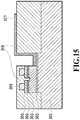
- FIG. 14 shows a top view of a conventional semiconductor optical modulator having an npin structure
- FIG. 15 shows a section XV-XV of FIG. 14
- FIG. 16 shows a section XVI-XVI of FIG. 14
- FIG. 17 shows a section XVII-XVII of FIG. 14
- a conventional semiconductor optical modulator has an n-type contact layer 302, an n-type cladding layer 303, a p-type carrier blocking layer 304, and a non-doped core/cladding layer 305 that are sequentially laminated on an SI-InP substrate 301. As shown in FIG.
- the non-doped core/cladding layer 305 is formed in such a manner as to configure a Mach-Zehnder interferometric waveguide.
- a semi-insulating (SI) cladding layer 306 is formed as shown in FIG. 15 and a region in which an n-type cladding layer 309 and an n-type contact layer 310 are formed as shown in FIG. 16 .
- the periphery of the waveguide is covered with an organic film 308 such as benzocyclobutene (BCB).
- BCB benzocyclobutene
- An electrode 307 is formed on the organic film 308 and connected to a lower n-type contact layer 302 and an upper n-type contact layer 310 exposed by partially etching the organic film 308.
- an npin structure especially has a problem in electrical surge resistance because, for example, (1) intermediate p layer potential is not fixed, (2) a charge tends to build up at an np junction, and (3) a breakdown tends to occur in a thin film p layer due to, for example, the tunnel effect.
- a block capacitor is provided near the device and electrically connected in parallel to the device, thereby increasing a stray capacity and improving the surge resistance.
- a method of adding a capacity to the semiconductor side mainly has two patterns: one is a method of providing a metal-insulator-metal (MIM) structure by sandwiching an insulating film between metal electrodes, and the other is a method of providing a pin diode structure directly under, for example, a feeding pad electrode having a large area other than the modulation region.
- MIM metal-insulator-metal
- PTL 1 Japanese Patent Laid-Open No. 2005-099387 Prior art is disclosed in document JP 2013 246223 A , describing a semiconductor optical phase modulator.
- NPL 1 K.-O. Velthaus, et al., "Impedance-Engineered Low Power MZM / Driver Assembly for CFP4-Size Pluggable Long Haul and Metro Transceiver," ECOC2014, Tu.1.1.1
- the former has a problem that it is difficult to create a larger capacity (e.g., 100 pF or more) than the stray capacity of the modulation region by using an MIM structure.
- a larger capacity e.g., 100 pF or more
- a pad electrode should have an area of 0.5 mm 2 or more, which becomes a major impediment to downsizing.
- the latter has a problem that the polarity of voltage applied to a pad electrode is limited due to the diode structure and a problem that even by taking a measure to provide, for example, a capacity of an npin structure directly under a pad region, although the maximum voltage value of ESD is reduced depending on the capacity ratio of a modulation section, the failure rate cannot be largely reduced with respect to reverse voltage ESD. That is, a fundamental solution to the improvement of the anti-surge characteristics requires such a structural measure that reverse voltage by ESD is not applied to the modulation region.
- An object of the present invention is to provide a highly reliable, high speed, and low loss semiconductor optical modulation element that protects a pin junction structure in a modulation region against reverse voltage ESD by configuring an additional capacity having a thyristor structure between a plurality of feeding pad electrodes.
- an aspect of the present invention is a semiconductor optical modulation element having an optical waveguide formed in a laminated structure having a pin junction in which at least a first cladding layer that is an n-type or p-type cladding layer, a non-doped core and cladding layer, and a second cladding layer that is a p-type or n-type cladding layer are laminated in this order on a semi-insulating substrate, the semiconductor optical modulation element comprising: a feeding electrode installation section formed on the laminated structure; and at least two feeding electrodes formed on the feeding electrode installation section, wherein the at least two feeding electrodes are connected to a modulation electrode installed on the optical waveguide, in the feeding electrode installation section, the second cladding layer and the non-doped core and cladding layer of the laminated structure are electrically isolated for each of the feeding electrodes so that the feeding electrodes are electrically isolated from each other, and the at least two feeding electrodes are electrically connected to each other via the
- Another aspect of the present invention is a semiconductor optical modulation element having an optical waveguide formed in a laminated structure having a pin junction in which at least a first cladding layer that is an n-type or p-type cladding layer, a non-doped core and cladding layer, and a second cladding layer that is a p-type or n-type cladding layer are laminated in this order on a semi-insulating substrate, the semiconductor optical modulation element comprising: a feeding electrode installation section formed on the laminated structure; and at least three feeding electrodes formed on the feeding electrode installation section, wherein at least two of the feeding electrodes are connected to a modulation electrode installed on the optical waveguide and at least one of the feeding electrodes is grounded, in the feeding electrode installation section, the second cladding layer and the non-doped core and cladding layer of the laminated structure are electrically isolated for each of the feeding electrodes so that the feeding electrodes are electrically isolated from one another, and at least the feeding electrodes connected to the modulation
- Another aspect of the present invention is a semiconductor optical modulation element having an optical waveguide formed in a laminated structure having a nipn junction or a pinp junction in which at least a first cladding layer that is an n-type or p-type cladding layer, a non-doped core and cladding layer, a p-type or n-type carrier blocking layer, and a second cladding layer that is an n-type or p-type cladding layer are laminated in this order on a semi-insulating substrate
- the semiconductor optical modulation element comprising: a feeding electrode installation section formed on the laminated structure; and at least two feeding electrodes formed on the feeding electrode installation section, wherein the at least two feeding electrodes are connected to a modulation electrode installed on the optical waveguide, in the feeding electrode installation section, the second cladding layer, the p-type or n-type carrier blocking layer, and the non-doped core and cladding layer of the laminated structure are electrically isolated for each of the feeding
- Another aspect of the present invention is a semiconductor optical modulation element having an optical waveguide formed in a laminated structure having a nipn junction or a pinp junction in which at least a first cladding layer that is an n-type or p-type cladding layer, a non-doped core and cladding layer, a p-type or n-type carrier blocking layer, and a second cladding layer that is an n-type or p-type cladding layer are laminated in this order on a semi-insulating substrate, the semiconductor optical modulation element comprising: a feeding electrode installation section formed on the laminated structure; and at least three feeding electrodes formed on the feeding electrode installation section, wherein at least two of the feeding electrodes are connected to a modulation electrode installed on the optical waveguide and at least one of the feeding electrodes is grounded, in the feeding electrode installation section, the second cladding layer, the p-type or n-type carrier blocking layer, and the non-doped core and cladding layer of the laminate
- the feeding electrodes connected to the modulation electrode are electrically connected to the at least one different grounded feeding electrode via the lower cladding layer.
- the optical waveguide configures a Mach-Zehnder optical interferometer.
- the modulation electrode has a capacity-loaded traveling-wave electrode structure.
- the present invention can protect a pin junction structure in a modulation region against reverse voltage ESD by configuring an additional capacity having a thyristor structure between a plurality of feeding electrodes electrodes in a semiconductor modulator having a pin junction.
- An example of a plurality of diodes reversely connected in series as a measure against ESD is a so-called thyristor structure such as an npnp or pnpn junction in which pn junctions are reversely connected in series.
- the thyristor structure has a mechanism in which forward voltage is definitely applied regardless of the porality of ESD applied, differently from the case of a pn junction alone. As a result, the thyristor structure has the effect in improving ESD resistance. Therefore, it can be said that addition of an additional circuit having this thyristor structure to a device is effective as a measure against ESD.
- At least one electrode in a feeding pad electrode group including a plurality of electrodes is connected to a ground at an initial stage of electrical mounting, whereby a thyristor structure can be configured by using the ground electrode even if ESD occurs via any electrode afterwards. As a result, ESD resistance can be improved in the subsequent mounting steps.
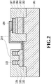
- FIG. 1 shows a top view of a high-speed modulator with a surge bypass circuit according to a first embodiment of the present invention.
- FIG. 2 shows a section II-II of FIG. 1
- FIG. 3 shows a section III-III of FIG. 1
- FIG. 4 shows a section IV-IV of FIG. 1 .
- a substrate 101 uses, for example, an SI-type InP (100) substrate as a sphalerite compound semiconductor crystal.
- An n-type contact layer 102, an n-type cladding layer 103, a non-doped core/cladding layer 104, a p-type cladding layer 106, and a p-type contact layer 107 are sequentially laminated on the substrate surface by epitaxial growth.
- a core layer of the core/cladding layer 104 uses a multiple quantum well structure (PL wavelength: 1.4 ⁇ m) including InGaAsP/InGaAsP period for efficient use of a change in refractive index by an electro-optic effect with respect to a wavelength in a 1.5 ⁇ m band.
- PL wavelength 1.4 ⁇ m
- InGaAsP/InGaAsP period for efficient use of a change in refractive index by an electro-optic effect with respect to a wavelength in a 1.5 ⁇ m band.
- composition of a cladding layer of the core/cladding layer 104 is, for example, InP having a lower refractive index than that of the core layer.
- InGaAs which lattice-matches InP and has a small energy band gap, is used for the n-type contact layer 102 and the p-type contact layer 107.
- each of the core and cladding Since it is only necessary for the composition of each of the core and cladding to have a refractive index contrast, there is clearly no problem even if InGaAlAs having a different composition is used for the core/cladding layer 104, the n-type cladding layer 103, and the p-type cladding layer 106, for example.
- the wavelength is not limited to the 1.5 ⁇ m band.
- the present invention does not lose its usefulness even if a 1.3 ⁇ m band is used.
- the conductive p-type cladding layer 106 and p-type contact layer 107 other than the modulation region and the feeding pad region are removed by dry etching and chemical etching, and then the non-doped cladding layer 105 (InP in this case) is deposited by crystal regrowth and backfilled with an organic film 109 such as BCB (e.g., FIG. 2 ).
- the modulation region is a region in which electrodes 108 of a Mach-Zehnder interferometric waveguide are formed and to which a high-frequency signal of the Mach-Zehnder interferometric waveguide or a direct voltage is applied.
- isolation is provided up to the core/cladding layer 104 by dry etching using an SiO 2 mask, thereby forming a Mach-Zehnder interferometric waveguide and a plurality of feeding pad installation sections.
- the n-type contact layer 102 and the n-type cladding layer 103 are removed by an etching process except for the modulation region of the Mach-Zehnder interferometric waveguide and the feeding region in which the feeding pad installation sections are formed so that the modulation region and the semiconductor of the lower part of the feeding region are electrically isolated.
- the BCB 109 forming the electrodes 108 is partially removed so as to expose the n-type contact layer 102 and the p-type contact layer 107.
- the electrodes 108 are formed from Au/Ti by, for example, vapor deposition and plating so that the electrodes 108 are electrically connected to the n-type contact layer 102 and the p-type contact layer 107.
- a plurality of feeding pads are formed on the common n-type contact layer 102 and n-type cladding layer 103 and a pinip junction is formed between the feeding pads.
- feeding pad electrodes may be electrically isolated from one another and at least one grounded feeding pad may be formed separately for each feeding pad, for example, as shown in FIG. 5 .
- the use of capacity-loaded traveling-wave electrodes enables higher speed modulation operation.
- the present invention does not lose its usefulness even in the case of a distributed constant line or a lumped constant line without the addition of a capacity.
- layers are laminated in the order of n-i-p from the substrate surface.
- the present invention does not lose its usefulness even if layers are laminated, for example, in the order of p-i-n from the substrate surface.
- the electrodes 108 are formed on two arm waveguides, respectively, in the modulation region of the Mach-Zehnder interferometric waveguide and three feeding pads are provided so as to be connected to an electrode for modulation.
- an electrode may be formed on only at least one of p-type contact layers 107 of arm waveguides and two feeding pads may be connected to an electrode for modulation.
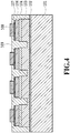
- FIG. 6 shows a top view of a high-speed modulator with a surge bypass circuit according to a second embodiment of the present invention.
- FIG. 7 shows a section VII-VII of FIG. 6
- FIG. 8 shows a section VIII-VIII of FIG. 6
- FIG. 9 shows a section IX-IX of FIG. 6 .
- the second embodiment is different from the first embodiment in that a nipn structure capable of configuring a higher speed and lower loss optical modulator is adopted as a semiconductor layer structure instead of a general pin structure.
- a nipn structure capable of configuring a higher speed and lower loss optical modulator is adopted as a semiconductor layer structure instead of a general pin structure.
- the ESD resistance can be improved by using the thyristor structure as an additional circuit.
- a substrate 201 uses, for example, an SI-type InP (100) substrate as a sphalerite compound semiconductor crystal.
- An n-type contact layer 202, an n-type cladding layer 203, a p-type carrier blocking layer 204, a non-doped core/cladding layer 205, an n-type cladding layer 207, and an n-type contact layer 208 are sequentially laminated on the substrate surface by epitaxial growth.
- a core layer of the core/cladding layer 205 uses a multiple quantum well structure (PL wavelength: 1.4 ⁇ m) including InGaAsP/InGaAsP period for efficient use of a change in refractive index by an electro-optic effect with respect to a wavelength in a 1.5 ⁇ m band.
- PL wavelength 1.4 ⁇ m
- InGaAsP/InGaAsP period for efficient use of a change in refractive index by an electro-optic effect with respect to a wavelength in a 1.5 ⁇ m band.
- composition of a cladding layer of the core/cladding layer 205 is, for example, InP having a lower refractive index than that of the core layer.
- InGaAs which lattice-matches InP and has a small energy band gap, is used for the n-type contact layers 202 and 208.
- each of the core and cladding Since it is only necessary for the composition of each of the core and cladding to have a refractive index contrast, there is clearly no problem even if InGaAlAs having a different composition is used for the core/cladding layer 205 and the n-type cladding layers 203 and 207, for example.
- the wavelength is not limited to the 1.5 ⁇ m band.
- the present invention does not lose its usefulness even if a 1.3 ⁇ m band is used.
- the conductive n-type cladding layer 207 and n-type contact layer 208 other than the modulation region and the feeding pad region are removed by dry etching and chemical etching, and then the semi-insulating (SI) cladding layer 206 (InP in this case) is deposited by crystal regrowth and backfilled (e.g., FIG. 7 ).
- SI semi-insulating
- isolation is provided up to the p-type carrier blocking layer 203 by dry etching using an SiO 2 mask, thereby forming a Mach-Zehnder interferometric waveguide and a plurality of feeding pad installation sections.
- the n-type contact layer 202 and the n-type cladding layer 203 are removed by an etching process except for the modulation region of the Mach-Zehnder interferometric waveguide and the feeding region in which the feeding pad installation sections are formed so that the modulation region and the semiconductor of the lower part of the feeding region are electrically isolated.
- the BCB 210 forming the electrodes 209 is partially removed so as to expose the n-type contact layer 202 and the n-type contact layer 208.
- the electrodes 209 are formed from Au/Ti by, for example, vapor deposition and plating so that the electrodes 209 are electrically connected to the n-type contact layer 202 and the n-type contact layer 208. Since a plurality of feeding pads are formed on the common n-type contact layer 202 and n-type cladding layer 203 and a npinipn junction including a thyristor structure is formed between the feeding pads, ESD externally applied to the feeding pads forms a junction.
- feeding pad electrodes may be electrically isolated from each other and at least one grounded electrode pad may be formed separately for each feeding pad, for example, as shown in FIG. 10 .
- the use of capacity-loaded traveling-wave electrodes enables higher speed modulation operation.
- the present invention does not lose its usefulness even in the case of a distributed constant line or a lumped constant line without the addition of a capacity.
- layers are laminated in the order of n-p-i-n from the substrate surface.
- the present invention does not lose its usefulness even in the case of laminating layers in the order of n-i-p-n from the substrate surface, for example.
- the waveguide structure of the modulation region is a waveguide in the form of a ridge.
- the present invention does not lose its usefulness even in the case of a waveguide having a high-mesa structure like the first embodiment, for example.
- the electrodes 209 are formed on two arm waveguides, respectively, in the modulation region of the Mach-Zehnder interferometric waveguide and three feeding pads are provided so as to be connected to an electrode for modulation.
- an electrode may be formed on only at least one of n-type contact layers 208 of arm waveguides and two feeding pads may be connected to an electrode for modulation.
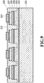
- FIG. 11 shows a top view of another high-speed modulator with a surge bypass circuit according to the second embodiment of the present invention.
- FIG. 12 shows a section XII-XII of FIG. 11
- FIG. 13 shows a section XIII-XIII of FIG. 11 .
- feeding pads may be formed so as to contact the substrate 201 exposed by removing the BCB 210, instead of providing feeding pads on a semiconductor layer structure. This can prevent the pn junction of the semiconductor layer structure from being broken by pressurization at the time of wire bonding.
- feeding pads are formed across the semiconductor layer structure on the feeding side from the Mach-Zehnder interferometric waveguide in FIGS. 11 to 13 , the feeding pads may be formed between the Mach-Zehnder interferometric waveguide and the semiconductor layer structure on the feeding side.
Description
- The present invention relates to a semiconductor optical modulation element with a surge bypass circuit capable of high speed modulation.
- In recent years, research and development of optical modulators using compound semiconductor materials are actively conducted with downsizing and speed enhancement of optical modulators as a backdrop. Among them, an optical modulator using InP as a substrate material can perform highly efficient modulation operation by using, for example, the quantum-confined Stark effect in a communication wavelength band. Attention is therefore being given to InP as a potential alternative modulator material to a conventional ferroelectric material.
- As a semiconductor optical modulator, an InP/InGaAsP optical modulator using a pin heterojunction to effectively apply voltage to a core of a waveguide together with optical confinement and an npin-type semiconductor optical modulator structure in which both InP cladding layers are of n-type for realization of a lower voltage drive optical modulator and a thin p-type semiconductor layer (p-type barrier layer) is inserted as a barrier layer for suppressing electron current are proposed (e.g., PTL 1).
- Since this npin type does not use a p-type cladding layer that is a factor causing optical loss, it enables the use of a relatively long waveguide and has the advantage in decreasing drive voltage. In addition, since the npin type has such a degree of freedom that the thickness of a depletion layer can be designed arbitrarily and optimally, it has the characteristics of easily satisfying matching of electrical impedancedance and matching of the speed of electricity and the speed of light at the same time and therefore being advantageous in speed enhancement.
- On the other hand, for reliability of semiconductor devices, it is impossible to neglect measures against electrostatic discharge (ESD). In a discussion about ESD in a diode device like a semiconductor, ESD should be divided into two polarities: so-called "forward voltage ESD" in which current flows by voltage application between pn junctions; and so-called "reverse voltage ESD" in which current does not flow (depletion).
- Since current generally flows through a diode in the case of forward voltage ESD, a failure rate is low there. In contrast, since current does not flow through a diode in reverse voltage ESD, a high electrical field is directly and momentarily applied to a depletion layer, which results in a rise in the failure rate. Therefore, in an ESD test for a normal device, ESD evaluation is often performed by using the polarity of reverse voltage.
-
FIG. 14 shows a top view of a conventional semiconductor optical modulator having an npin structure,FIG. 15 shows a section XV-XV ofFIG. 14 ,FIG. 16 shows a section XVI-XVI ofFIG. 14 , andFIG. 17 shows a section XVII-XVII ofFIG. 14 . A conventional semiconductor optical modulator has an n-type contact layer 302, an n-type cladding layer 303, a p-typecarrier blocking layer 304, and a non-doped core/cladding layer 305 that are sequentially laminated on an SI-InP substrate 301. As shown inFIG. 15 , the non-doped core/cladding layer 305 is formed in such a manner as to configure a Mach-Zehnder interferometric waveguide. On the non-doped core/cladding layer 305, there are a region in which a semi-insulating (SI)cladding layer 306 is formed as shown inFIG. 15 and a region in which an n-type cladding layer 309 and an n-type contact layer 310 are formed as shown inFIG. 16 . The periphery of the waveguide is covered with anorganic film 308 such as benzocyclobutene (BCB). - An
electrode 307 is formed on theorganic film 308 and connected to a lower n-type contact layer 302 and an upper n-type contact layer 310 exposed by partially etching theorganic film 308. - In such a conventional semiconductor optical modulator, since a capacity of a pn junction of a modulation region is predominant in a stray capacity of a device, a high electrical field by ESD is mostly applied to the pn junction. This results in an increase in the probability of causing a diode failure in the modulation region to be the core of the device.
- In particular, differently from a conventional pin structure (e.g., NPL 1), an npin structure especially has a problem in electrical surge resistance because, for example, (1) intermediate p layer potential is not fixed, (2) a charge tends to build up at an np junction, and (3) a breakdown tends to occur in a thin film p layer due to, for example, the tunnel effect.
- In general, for improvement of the anti-surge characteristics of a semiconductor device, a block capacitor is provided near the device and electrically connected in parallel to the device, thereby increasing a stray capacity and improving the surge resistance.
- However, if a surge is applied to the semiconductor device before the block capacitor is mounted/provided, the probability of causing a surge failure increases. For this reason, it is preferable that an additional capacity be not added at the mounting step but be built at the stage of a semiconductor wafer process.
- A method of adding a capacity to the semiconductor side mainly has two patterns: one is a method of providing a metal-insulator-metal (MIM) structure by sandwiching an insulating film between metal electrodes, and the other is a method of providing a pin diode structure directly under, for example, a feeding pad electrode having a large area other than the modulation region.
- PTL 1:
Japanese Patent Laid-Open No. 2005-099387
Prior art is disclosed in documentJP 2013 246223 A - NPL 1: K.-O. Velthaus, et al., "Impedance-Engineered Low Power MZM / Driver Assembly for CFP4-Size Pluggable Long Haul and Metro Transceiver," ECOC2014, Tu.1.1.1
- However, the former has a problem that it is difficult to create a larger capacity (e.g., 100 pF or more) than the stray capacity of the modulation region by using an MIM structure. For example, if an insulator is SiO2 of 200 nm (relative permittivity 4.2), a pad electrode should have an area of 0.5 mm2 or more, which becomes a major impediment to downsizing.
- In addition, the latter has a problem that the polarity of voltage applied to a pad electrode is limited due to the diode structure and a problem that even by taking a measure to provide, for example, a capacity of an npin structure directly under a pad region, although the maximum voltage value of ESD is reduced depending on the capacity ratio of a modulation section, the failure rate cannot be largely reduced with respect to reverse voltage ESD. That is, a fundamental solution to the improvement of the anti-surge characteristics requires such a structural measure that reverse voltage by ESD is not applied to the modulation region.
- The present invention has been accomplished in consideration of the above problems. An object of the present invention is to provide a highly reliable, high speed, and low loss semiconductor optical modulation element that protects a pin junction structure in a modulation region against reverse voltage ESD by configuring an additional capacity having a thyristor structure between a plurality of feeding pad electrodes.
- In order to solve the above problems, an aspect of the present invention is a semiconductor optical modulation element having an optical waveguide formed in a laminated structure having a pin junction in which at least a first cladding layer that is an n-type or p-type cladding layer, a non-doped core and cladding layer, and a second cladding layer that is a p-type or n-type cladding layer are laminated in this order on a semi-insulating substrate, the semiconductor optical modulation element comprising: a feeding electrode installation section formed on the laminated structure; and at least two feeding electrodes formed on the feeding electrode installation section, wherein the at least two feeding electrodes are connected to a modulation electrode installed on the optical waveguide, in the feeding electrode installation section, the second cladding layer and the non-doped core and cladding layer of the laminated structure are electrically isolated for each of the feeding electrodes so that the feeding electrodes are electrically isolated from each other, and the at least two feeding electrodes are electrically connected to each other via the first cladding layer of the laminated structure, and the optical waveguide and the feeding electrode installation section are electrically isolated in terms of the laminated structure, and wherein the feeding electrode has a feeding pad formed to contact the semi-insulating substrate.
- Another aspect of the present invention is a semiconductor optical modulation element having an optical waveguide formed in a laminated structure having a pin junction in which at least a first cladding layer that is an n-type or p-type cladding layer, a non-doped core and cladding layer, and a second cladding layer that is a p-type or n-type cladding layer are laminated in this order on a semi-insulating substrate, the semiconductor optical modulation element comprising: a feeding electrode installation section formed on the laminated structure; and at least three feeding electrodes formed on the feeding electrode installation section, wherein at least two of the feeding electrodes are connected to a modulation electrode installed on the optical waveguide and at least one of the feeding electrodes is grounded, in the feeding electrode installation section, the second cladding layer and the non-doped core and cladding layer of the laminated structure are electrically isolated for each of the feeding electrodes so that the feeding electrodes are electrically isolated from one another, and at least the feeding electrodes connected to the modulation electrode and the grounded feeding electrode are electrically connected to each other via the first cladding layer of the laminated structure, and the optical waveguide and the feeding electrode installation section are electrically isolated in terms of the laminated structure, and wherein the feeding electrode has a feeding pad formed to contact the semi-insulating substrate.
- Another aspect of the present invention is a semiconductor optical modulation element having an optical waveguide formed in a laminated structure having a nipn junction or a pinp junction in which at least a first cladding layer that is an n-type or p-type cladding layer, a non-doped core and cladding layer, a p-type or n-type carrier blocking layer, and a second cladding layer that is an n-type or p-type cladding layer are laminated in this order on a semi-insulating substrate, the semiconductor optical modulation element comprising: a feeding electrode installation section formed on the laminated structure; and at least two feeding electrodes formed on the feeding electrode installation section, wherein the at least two feeding electrodes are connected to a modulation electrode installed on the optical waveguide, in the feeding electrode installation section, the second cladding layer, the p-type or n-type carrier blocking layer, and the non-doped core and cladding layer of the laminated structure are electrically isolated for each of the feeding electrodes so that the feeding electrodes are electrically isolated from each other, and the at least two feeding electrodes are electrically connected to each other via the first cladding layer of the laminated structure, and the optical waveguide and the feeding electrode installation section are electrically isolated in terms of the laminated structure, and wherein the feeding electrode has a feeding pad formed to contact the semi-insulating substrate.
- Another aspect of the present invention is a semiconductor optical modulation element having an optical waveguide formed in a laminated structure having a nipn junction or a pinp junction in which at least a first cladding layer that is an n-type or p-type cladding layer, a non-doped core and cladding layer, a p-type or n-type carrier blocking layer, and a second cladding layer that is an n-type or p-type cladding layer are laminated in this order on a semi-insulating substrate, the semiconductor optical modulation element comprising: a feeding electrode installation section formed on the laminated structure; and at least three feeding electrodes formed on the feeding electrode installation section, wherein at least two of the feeding electrodes are connected to a modulation electrode installed on the optical waveguide and at least one of the feeding electrodes is grounded, in the feeding electrode installation section, the second cladding layer, the p-type or n-type carrier blocking layer, and the non-doped core and cladding layer of the laminated structure are electrically isolated for each of the feeding electrodes so that the feeding electrodes are electrically isolated from each other, and the feeding electrodes connected to the modulation electrode and the grounded feeding electrode are electrically connected to each other via the second cladding layer of the laminated structure, and the optical waveguide and the feeding electrode installation section are electrically isolated in terms of the laminated structure, and wherein the feeding electrode has a feeding pad formed to contact the semi-insulating substrate.
- According to another aspect of the present invention, the feeding electrodes connected to the modulation electrode are electrically connected to the at least one different grounded feeding electrode via the lower cladding layer.
- According to another aspect of the present invention, the optical waveguide configures a Mach-Zehnder optical interferometer.
- According to another aspect of the present invention, the modulation electrode has a capacity-loaded traveling-wave electrode structure.
- The present invention can protect a pin junction structure in a modulation region against reverse voltage ESD by configuring an additional capacity having a thyristor structure between a plurality of feeding electrodes electrodes in a semiconductor modulator having a pin junction.
-
- [
FIG. 1] FIG. 1 is a top view of a high-speed modulator with a surge bypass circuit according to a first embodiment of the present invention; - [
FIG. 2] FIG. 2 is a section II-II ofFIG. 1 ; - [
FIG. 3] FIG. 3 is a section III-III ofFIG. 1 ; - [
FIG. 4] FIG. 4 is a section IV-IV ofFIG. 1 ; - [
FIG. 5] FIG. 5 is a top view of another high-speed modulator with a surge bypass circuit according to a first embodiment of the present invention; - [
FIG. 6] FIG. 6 is a top view of a high-speed modulator with a surge bypass circuit according to a second embodiment of the present invention; - [
FIG. 7] FIG. 7 is a section VII-VII ofFIG. 6 ; - [
FIG. 8] FIG. 8 is a section VIII-VIII ofFIG. 6 ; - [
FIG. 9] FIG. 9 is a section IX-IX ofFIG. 6 ; - [
FIG. 10] FIG. 10 is a top view of another high-speed modulator with a surge bypass circuit according to the second embodiment of the present invention; - [
FIG. 11] FIG. 11 is a top view of yet another high-speed modulator with a surge bypass circuit according to the second embodiment of the present invention; - [
FIG. 12] FIG. 12 is a section XII-XII ofFIG. 11 ; - [
FIG. 13] FIG. 13 is a section XIII-XIII ofFIG. 11 ; - [
FIG. 14] FIG. 14 is a top view of a conventional semiconductor optical modulator having an npin structure; - [
FIG. 15] FIG. 15 is a section XV-XV ofFIG. 14 ; - [
FIG. 16] FIG. 16 is a section XVI-XVI ofFIG. 14 ; and - [
FIG. 17] FIG. 17 is a section XVII-XVII ofFIG. 14 . - In the present invention, attention is focused on forward voltage ESD with a low ESD failure rate as a measure against ESD (reverse voltage ESD) in a pn diode structure device. That is, as a measure against ESD, a plurality of diodes are reversely connected in series. Accordingly, even if voltage to be reverse voltage ESD to a modulation region is applied to a device circuit, the voltage becomes forward voltage to any of the diodes in the circuit and a charge is consumed there. This can largely reduce the reverse voltage applied to the other diodes including the modulation region.
- An example of a plurality of diodes reversely connected in series as a measure against ESD is a so-called thyristor structure such as an npnp or pnpn junction in which pn junctions are reversely connected in series. The thyristor structure has a mechanism in which forward voltage is definitely applied regardless of the porality of ESD applied, differently from the case of a pn junction alone. As a result, the thyristor structure has the effect in improving ESD resistance. Therefore, it can be said that addition of an additional circuit having this thyristor structure to a device is effective as a measure against ESD.
- In addition, even if voltage of an arbitrary polarity is applied to electrodes at both ends including the thyristor structure, current hardly flows there. Therefore, even if the structure is provided in a feeding pad region, no limitation is imposed on the polarity of the voltage to be applied to the feeding pad.
- Further, at least one electrode in a feeding pad electrode group including a plurality of electrodes is connected to a ground at an initial stage of electrical mounting, whereby a thyristor structure can be configured by using the ground electrode even if ESD occurs via any electrode afterwards. As a result, ESD resistance can be improved in the subsequent mounting steps.
- Embodiments of the present invention will be described below with reference to the drawings.
-
FIG. 1 shows a top view of a high-speed modulator with a surge bypass circuit according to a first embodiment of the present invention.FIG. 2 shows a section II-II ofFIG. 1 ,FIG. 3 shows a section III-III ofFIG. 1 , andFIG. 4 shows a section IV-IV ofFIG. 1 . - A
substrate 101 uses, for example, an SI-type InP (100) substrate as a sphalerite compound semiconductor crystal. An n-type contact layer 102, an n-type cladding layer 103, a non-doped core/cladding layer 104, a p-type cladding layer 106, and a p-type contact layer 107 are sequentially laminated on the substrate surface by epitaxial growth. - A core layer of the core/
cladding layer 104 uses a multiple quantum well structure (PL wavelength: 1.4 µm) including InGaAsP/InGaAsP period for efficient use of a change in refractive index by an electro-optic effect with respect to a wavelength in a 1.5 µm band. - The composition of a cladding layer of the core/
cladding layer 104 is, for example, InP having a lower refractive index than that of the core layer. InGaAs, which lattice-matches InP and has a small energy band gap, is used for the n-type contact layer 102 and the p-type contact layer 107. - Since it is only necessary for the composition of each of the core and cladding to have a refractive index contrast, there is clearly no problem even if InGaAlAs having a different composition is used for the core/
cladding layer 104, the n-type cladding layer 103, and the p-type cladding layer 106, for example. - Further, the wavelength is not limited to the 1.5 µm band. For example, the present invention does not lose its usefulness even if a 1.3 µm band is used.
- For electrical isolation between electrodes, the conductive p-
type cladding layer 106 and p-type contact layer 107 other than the modulation region and the feeding pad region are removed by dry etching and chemical etching, and then the non-doped cladding layer 105 (InP in this case) is deposited by crystal regrowth and backfilled with anorganic film 109 such as BCB (e.g.,FIG. 2 ). The modulation region is a region in whichelectrodes 108 of a Mach-Zehnder interferometric waveguide are formed and to which a high-frequency signal of the Mach-Zehnder interferometric waveguide or a direct voltage is applied. - Next, as shown in
FIGS. 1 and4 , isolation is provided up to the core/cladding layer 104 by dry etching using an SiO2 mask, thereby forming a Mach-Zehnder interferometric waveguide and a plurality of feeding pad installation sections. After that, as shown inFIGS. 2 and3 , the n-type contact layer 102 and the n-type cladding layer 103 are removed by an etching process except for the modulation region of the Mach-Zehnder interferometric waveguide and the feeding region in which the feeding pad installation sections are formed so that the modulation region and the semiconductor of the lower part of the feeding region are electrically isolated. - After the upper surface is planarized by the
BCB 109, theBCB 109 forming theelectrodes 108 is partially removed so as to expose the n-type contact layer 102 and the p-type contact layer 107. Theelectrodes 108 are formed from Au/Ti by, for example, vapor deposition and plating so that theelectrodes 108 are electrically connected to the n-type contact layer 102 and the p-type contact layer 107. A plurality of feeding pads are formed on the common n-type contact layer 102 and n-type cladding layer 103 and a pinip junction is formed between the feeding pads. - Next, in the case of performing, for example, Au wire bonding for the feeding pads of the
electrodes 108, it is preferable that at least one of the feeding pads be initially connected to a ground as shown inFIG. 1 . This enables connection including a pinip junction between the grounded pads even if ESD is applied to any feeding pad. Even in the absence of a feeding pad for ground connection, specifying the order of connecting Au wires (for example, a feeding pad for lower n-type cladding is finally connected to a wire) can prevent the present invention from losing its usefulness. Instead of the feeding pad electrode pattern shown inFIG. 1 , feeding pad electrodes may be electrically isolated from one another and at least one grounded feeding pad may be formed separately for each feeding pad, for example, as shown inFIG. 5 . - When driving the element as a modulator, the use of capacity-loaded traveling-wave electrodes enables higher speed modulation operation. However, it is clear that the present invention does not lose its usefulness even in the case of a distributed constant line or a lumped constant line without the addition of a capacity.
- Further, in the present embodiment, layers are laminated in the order of n-i-p from the substrate surface. However, it is clear that the present invention does not lose its usefulness even if layers are laminated, for example, in the order of p-i-n from the substrate surface.
- Further, in the present embodiment, the
electrodes 108 are formed on two arm waveguides, respectively, in the modulation region of the Mach-Zehnder interferometric waveguide and three feeding pads are provided so as to be connected to an electrode for modulation. However, an electrode may be formed on only at least one of p-type contact layers 107 of arm waveguides and two feeding pads may be connected to an electrode for modulation. -
FIG. 6 shows a top view of a high-speed modulator with a surge bypass circuit according to a second embodiment of the present invention.FIG. 7 shows a section VII-VII ofFIG. 6 ,FIG. 8 shows a section VIII-VIII ofFIG. 6 , andFIG. 9 shows a section IX-IX ofFIG. 6 . The second embodiment is different from the first embodiment in that a nipn structure capable of configuring a higher speed and lower loss optical modulator is adopted as a semiconductor layer structure instead of a general pin structure. As described above, even in the case of this structure having a problem in ESD resistance as compared with the pin structure, the ESD resistance can be improved by using the thyristor structure as an additional circuit. - A
substrate 201 uses, for example, an SI-type InP (100) substrate as a sphalerite compound semiconductor crystal. An n-type contact layer 202, an n-type cladding layer 203, a p-typecarrier blocking layer 204, a non-doped core/cladding layer 205, an n-type cladding layer 207, and an n-type contact layer 208 are sequentially laminated on the substrate surface by epitaxial growth. - A core layer of the core/
cladding layer 205 uses a multiple quantum well structure (PL wavelength: 1.4 µm) including InGaAsP/InGaAsP period for efficient use of a change in refractive index by an electro-optic effect with respect to a wavelength in a 1.5 µm band. - The composition of a cladding layer of the core/
cladding layer 205 is, for example, InP having a lower refractive index than that of the core layer. InGaAs, which lattice-matches InP and has a small energy band gap, is used for the n-type contact layers 202 and 208. - Since it is only necessary for the composition of each of the core and cladding to have a refractive index contrast, there is clearly no problem even if InGaAlAs having a different composition is used for the core/
cladding layer 205 and the n-type cladding layers 203 and 207, for example. - Further, the wavelength is not limited to the 1.5 µm band. For example, the present invention does not lose its usefulness even if a 1.3 µm band is used.
- For electrical isolation between electrodes, the conductive n-
type cladding layer 207 and n-type contact layer 208 other than the modulation region and the feeding pad region are removed by dry etching and chemical etching, and then the semi-insulating (SI) cladding layer 206 (InP in this case) is deposited by crystal regrowth and backfilled (e.g.,FIG. 7 ). - Next, as shown in
FIGS. 6 and9 , isolation is provided up to the p-typecarrier blocking layer 203 by dry etching using an SiO2 mask, thereby forming a Mach-Zehnder interferometric waveguide and a plurality of feeding pad installation sections. After that, as shown inFIGS. 7 and8 , the n-type contact layer 202 and the n-type cladding layer 203 are removed by an etching process except for the modulation region of the Mach-Zehnder interferometric waveguide and the feeding region in which the feeding pad installation sections are formed so that the modulation region and the semiconductor of the lower part of the feeding region are electrically isolated. - After the upper surface is planarized by an organic film such as BCB, the
BCB 210 forming theelectrodes 209 is partially removed so as to expose the n-type contact layer 202 and the n-type contact layer 208. Theelectrodes 209 are formed from Au/Ti by, for example, vapor deposition and plating so that theelectrodes 209 are electrically connected to the n-type contact layer 202 and the n-type contact layer 208. Since a plurality of feeding pads are formed on the common n-type contact layer 202 and n-type cladding layer 203 and a npinipn junction including a thyristor structure is formed between the feeding pads, ESD externally applied to the feeding pads forms a junction. - Next, in the case of performing, for example, Au wire bonding for the feeding pads of the
electrodes 209, it is preferable that at least one of the feeding pads be initially connected to a ground as shown inFIG. 6 , whereby connection including a thyristor structure can be made between the grounded pads even if ESD is applied to any feeding pad. Even in the absence of a pad connected to a ground, specifying the order of connecting Au wires (for example, a feeding pad for lower n-type cladding is finally connected to a wire) can prevent the present invention from losing its usefulness. Instead of the feeding pad electrode pattern shown inFIG. 6 , feeding pad electrodes may be electrically isolated from each other and at least one grounded electrode pad may be formed separately for each feeding pad, for example, as shown inFIG. 10 . - When driving the element as a modulator, the use of capacity-loaded traveling-wave electrodes enables higher speed modulation operation. However, it is clear that the present invention does not lose its usefulness even in the case of a distributed constant line or a lumped constant line without the addition of a capacity.
- Further, in the present embodiment, layers are laminated in the order of n-p-i-n from the substrate surface. However, it is clear that the present invention does not lose its usefulness even in the case of laminating layers in the order of n-i-p-n from the substrate surface, for example.
- Further, in the present embodiment, the waveguide structure of the modulation region is a waveguide in the form of a ridge. However, it is clear that the present invention does not lose its usefulness even in the case of a waveguide having a high-mesa structure like the first embodiment, for example.
- Further, in the present embodiment, the
electrodes 209 are formed on two arm waveguides, respectively, in the modulation region of the Mach-Zehnder interferometric waveguide and three feeding pads are provided so as to be connected to an electrode for modulation. However, an electrode may be formed on only at least one of n-type contact layers 208 of arm waveguides and two feeding pads may be connected to an electrode for modulation. - Further,
FIG. 11 shows a top view of another high-speed modulator with a surge bypass circuit according to the second embodiment of the present invention.FIG. 12 shows a section XII-XII ofFIG. 11 andFIG. 13 shows a section XIII-XIII ofFIG. 11 . In the structure shown inFIGS. 11 to 13 , feeding pads may be formed so as to contact thesubstrate 201 exposed by removing theBCB 210, instead of providing feeding pads on a semiconductor layer structure. This can prevent the pn junction of the semiconductor layer structure from being broken by pressurization at the time of wire bonding. Although feeding pads are formed across the semiconductor layer structure on the feeding side from the Mach-Zehnder interferometric waveguide inFIGS. 11 to 13 , the feeding pads may be formed between the Mach-Zehnder interferometric waveguide and the semiconductor layer structure on the feeding side. - The configuration in which the feeding pads are formed not on the semiconductor layer structure but directly on the
substrate 201 has been described by using the second embodiment as an example, but it is needless to say that the same advantageous result can be achieved by forming the feeding pads directly on thesubstrate 101 also in the first embodiment. -
- 101, 201
- substrate
- 102, 202, 208
- n-type contact layer
- 103, 203, 207
- n-type cladding layer
- 104, 205
- non-doped core/cladding layer
- 105
- non-doped cladding layer
- 106
- p-type cladding layer
- 107
- p-type contact layer
- 108, 209
- electrode
- 109, 210
- BCB
- 204
- p-type carrier blocking layer
- 206
- SI cladding layer
- 301
- substrate
- 302
- n-type contact layer
- 303
- n-type cladding layer
- 304
- p-type carrier blocking layer
- 305
- non-doped core/cladding layer
- 306
- SI cladding layer
- 307
- electrode
- 308
- BCB
Claims (7)
- A semiconductor optical modulation element having an optical waveguide formed in a laminated structure having a pin junction in which at least a first cladding layer (105; 106) that is an n-type or p-type cladding layer, a non-doped core and cladding layer (104), and a second cladding layer (103) that is a p-type or n-type cladding layer are laminated in this order on a semi-insulating substrate (101), the semiconductor optical modulation element comprising:a feeding electrode installation section formed on the laminated structure; andat least two feeding electrodes (108) formed on the feeding electrode installation section,wherein the at least two feeding electrodes (108) are connected to a modulation electrode installed on the optical waveguide,in the feeding electrode installation section, the second cladding layer (103) and the non-doped core and cladding layer (104) of the laminated structure are electrically isolated for each of the feeding electrodes (108) so that the feeding electrodes (108) are electrically isolated from each other, and the at least two feeding electrodes (108) are electrically connected to each other via the first cladding layer (105; 106) of the laminated structure, andthe optical waveguide and the feeding electrode installation section are electrically isolated in terms of the laminated structure,characterized in thatthe feeding electrode (108) has a feeding pad formed to contact the semi-insulating substrate (101).
- A semiconductor optical modulation element having an optical waveguide formed in a laminated structure having a pin junction in which at least a first cladding layer (105; 106) that is an n-type or p-type cladding layer, a non-doped core and cladding layer (104), and a second cladding layer (103) that is a p-type or n-type cladding layer are laminated in this order on a semi-insulating substrate (101), the semiconductor optical modulation element comprising:a feeding electrode installation section formed on the laminated structure; andat least three feeding electrodes (108) formed on the feeding electrode installation section,wherein at least two of the feeding electrodes (108) are connected to a modulation electrode installed on the optical waveguide and at least one of the feeding electrodes (108) is grounded,in the feeding electrode installation section, the second cladding layer (103) and the non-doped core and cladding layer (104) of the laminated structure are electrically isolated for each of the feeding electrodes (108) so that the feeding electrodes (108) are electrically isolated from one another, and at least the feeding electrodes (108) connected to the modulation electrode and the grounded feeding electrode (108) are electrically connected to each other via the first cladding layer (105; 106) of the laminated structure, andthe optical waveguide and the feeding electrode installation section are electrically isolated in terms of the laminated structure,characterized in thatthe feeding electrode (108) has a feeding pad formed to contact the semi-insulating substrate (101).
- A semiconductor optical modulation element having an optical waveguide formed in a laminated structure having a nipn junction or a pinp junction in which at least a first cladding layer (206; 207; 306) that is an n-type or p-type cladding layer, a non-doped core and cladding layer (205; 305), a p-type or n-type carrier blocking layer (204; 304), and a second cladding layer (203; 303) that is an n-type or p-type cladding layer are laminated in this order on a semi-insulating substrate (201; 301), the semiconductor optical modulation element comprising:a feeding electrode installation section formed on the laminated structure; andat least two feeding electrodes (209; 307) formed on the feeding electrode installation section,wherein the at least two feeding electrodes (209; 307) are connected to a modulation electrode installed on the optical waveguide,in the feeding electrode installation section, the second cladding layer (203; 303), the p-type or n-type carrier blocking layer (204; 304), and the non-doped core and cladding layer (205; 305) of the laminated structure are electrically isolated for each of the feeding electrodes (209; 307) so that the feeding electrodes are electrically isolated from each other, and the at least two feeding electrodes (209; 307) are electrically connected to each other via the first cladding layer (206; 207; 306) of the laminated structure, andthe optical waveguide and the feeding electrode installation section are electrically isolated in terms of the laminated structure,characterized in thatthe feeding electrode (209; 307) has a feeding pad formed to contact the semi-insulating substrate (201; 301).
- A semiconductor optical modulation element having an optical waveguide formed in a laminated structure having a nipn junction or a pinp junction in which at least a first cladding layer (206; 207; 306) that is an n-type or p-type cladding layer, a non-doped core and cladding layer (205; 305), a p-type or n-type carrier blocking layer (204; 304), and a second cladding layer (203; 303) that is an n-type or p-type cladding layer are laminated in this order on a semi-insulating substrate (201; 301), the semiconductor optical modulation element comprising:a feeding electrode installation section formed on the laminated structure; andat least three feeding electrodes (209; 307) formed on the feeding electrode installation section,wherein at least two of the feeding electrodes (209; 307) are connected to a modulation electrode installed on the optical waveguide and at least one of the feeding electrodes (209; 307) is grounded,in the feeding electrode installation section, the second cladding layer (203; 303), the p-type or n-type carrier blocking layer (204; 304), and the non-doped core and cladding layer (205; 305) of the laminated structure are electrically isolated for each of the feeding electrodes (209; 307) so that the feeding electrodes (209; 307) are electrically isolated from each other, and the feeding electrodes (209; 307) connected to the modulation electrode and the grounded feeding electrode (209; 307) are electrically connected to each other via the second cladding layer (203; 303) of the laminated structure, andthe optical waveguide and the feeding electrode installation section are electrically isolated in terms of the laminated structure,characterized in thatthe feeding electrode (209; 307) has a feeding pad formed to contact the semi-insulating substrate (201; 301).
- The semiconductor optical modulation element according to claim 2 or 4, wherein each of the feeding electrodes (108; 209; 307) connected to the modulation electrode is electrically connected to the at least one different grounded feeding electrode (108; 209; 307) via the first cladding layer (105; 106; 206; 207; 306).
- The semiconductor optical modulation element according to any one of claims 1 to 5, wherein the optical waveguide configures a Mach-Zehnder optical interferometer.
- The semiconductor optical modulation element according to any one of claims 1 to 6, wherein the modulation electrode has a capacity-loaded traveling-wave electrode structure.
Applications Claiming Priority (2)
| Application Number | Priority Date | Filing Date | Title |
|---|---|---|---|
| JP2016178905 | 2016-09-13 | ||
| PCT/JP2017/033014 WO2018052013A1 (en) | 2016-09-13 | 2017-09-13 | Semiconductor optical modulation element |
Publications (3)
| Publication Number | Publication Date |
|---|---|
| EP3514616A1 EP3514616A1 (en) | 2019-07-24 |
| EP3514616A4 EP3514616A4 (en) | 2020-06-03 |
| EP3514616B1 true EP3514616B1 (en) | 2021-08-04 |
Family
ID=61619546
Family Applications (1)
| Application Number | Title | Priority Date | Filing Date |
|---|---|---|---|
| EP17850914.7A Active EP3514616B1 (en) | 2016-09-13 | 2017-09-13 | Semiconductor optical modulation element |
Country Status (7)
| Country | Link |
|---|---|
| US (1) | US11126058B1 (en) |
| EP (1) | EP3514616B1 (en) |
| JP (1) | JP6592610B2 (en) |
| CN (1) | CN109690392B (en) |
| CA (1) | CA3036468C (en) |
| TW (1) | TWI632413B (en) |
| WO (1) | WO2018052013A1 (en) |
Families Citing this family (4)
| Publication number | Priority date | Publication date | Assignee | Title |
|---|---|---|---|---|
| JP7110879B2 (en) * | 2018-09-28 | 2022-08-02 | 住友電気工業株式会社 | Semiconductor device and its manufacturing method |
| WO2020245618A2 (en) * | 2019-05-20 | 2020-12-10 | 华为技术(美国)有限公司 | Electro-optic modulator, optical component, and optical module |
| JP7404711B2 (en) * | 2019-08-23 | 2023-12-26 | 住友電気工業株式会社 | light modulator |
| CN114114721A (en) * | 2020-08-25 | 2022-03-01 | 住友电气工业株式会社 | Optical modulator |
Family Cites Families (12)
| Publication number | Priority date | Publication date | Assignee | Title |
|---|---|---|---|---|
| JPS5919389A (en) | 1982-07-24 | 1984-01-31 | Fujitsu Ltd | Semiconductor device |
| JP2754957B2 (en) * | 1991-07-10 | 1998-05-20 | 日本電気株式会社 | Semiconductor light control element and method of manufacturing the same |
| US5914501A (en) * | 1998-08-27 | 1999-06-22 | Hewlett-Packard Company | Light emitting diode assembly having integrated electrostatic discharge protection |
| US6977954B2 (en) * | 2003-07-25 | 2005-12-20 | University Of Connecticut | Semiconductor laser array device employing modulation doped quantum well structures |
| JP4047785B2 (en) | 2003-09-24 | 2008-02-13 | Nttエレクトロニクス株式会社 | Semiconductor optoelectronic waveguide |
| DE102004005269B4 (en) | 2003-11-28 | 2005-09-29 | Osram Opto Semiconductors Gmbh | Light emitting semiconductor element has multilayers on a substrate with the pn junction insulatively separated into light emitting and protective diode sections |
| JP2005217381A (en) * | 2004-02-02 | 2005-08-11 | Sony Corp | Semiconductor light emitting device and its manufacturing method |
| US7462884B2 (en) * | 2005-10-31 | 2008-12-09 | Nichia Corporation | Nitride semiconductor device |
| JP2010287604A (en) * | 2009-06-09 | 2010-12-24 | Nec Corp | Waveguide optical element and method of manufacturing the same |
| JP2011191343A (en) * | 2010-03-11 | 2011-09-29 | Seiko Epson Corp | Display sheet, display device and electronic apparatus |
| JP5118166B2 (en) * | 2010-03-19 | 2013-01-16 | 日本電信電話株式会社 | Semiconductor optical modulator with built-in surge protection function and method for manufacturing the same |
| JP5705786B2 (en) * | 2012-05-24 | 2015-04-22 | 日本電信電話株式会社 | Semiconductor optical phase modulator |
-
2017
- 2017-09-13 JP JP2018539743A patent/JP6592610B2/en active Active
- 2017-09-13 CA CA3036468A patent/CA3036468C/en active Active
- 2017-09-13 US US16/332,740 patent/US11126058B1/en active Active
- 2017-09-13 WO PCT/JP2017/033014 patent/WO2018052013A1/en unknown
- 2017-09-13 CN CN201780056209.1A patent/CN109690392B/en active Active
- 2017-09-13 TW TW106131436A patent/TWI632413B/en active
- 2017-09-13 EP EP17850914.7A patent/EP3514616B1/en active Active
Also Published As
| Publication number | Publication date |
|---|---|
| JP6592610B2 (en) | 2019-10-16 |
| US20210294176A1 (en) | 2021-09-23 |
| WO2018052013A1 (en) | 2018-03-22 |
| CN109690392A (en) | 2019-04-26 |
| TWI632413B (en) | 2018-08-11 |
| EP3514616A4 (en) | 2020-06-03 |
| TW201825971A (en) | 2018-07-16 |
| EP3514616A1 (en) | 2019-07-24 |
| CA3036468A1 (en) | 2018-03-22 |
| CN109690392B (en) | 2022-05-03 |
| JPWO2018052013A1 (en) | 2019-02-14 |
| US11126058B1 (en) | 2021-09-21 |
| CA3036468C (en) | 2022-05-03 |
Similar Documents
| Publication | Publication Date | Title |
|---|---|---|
| EP3514616B1 (en) | Semiconductor optical modulation element | |
| EP3306381B1 (en) | Semiconductor optical modulation element | |
| JP4870518B2 (en) | Semiconductor optical modulator | |
| US20020071621A1 (en) | Semiconductor optical function device | |
| JP4750764B2 (en) | Semiconductor optical modulator | |
| JP4901126B2 (en) | Electroabsorption modulator and manufacturing method thereof | |
| EP3739635A1 (en) | A device comprising an active component and associated electrodes and a method of manufacturing such device | |
| US20240006844A1 (en) | Semiconductor Optical Device | |
| WO2023233718A1 (en) | Semiconductor light-receiving element | |
| CN111308739B (en) | Optical modulator | |
| US11300850B2 (en) | Mach-Zehnder modulator | |
| CN112415787A (en) | Optical modulator | |
| US20130234112A1 (en) | Semiconductor optical modulator | |
| US20220399471A1 (en) | Optical Receiving Element and Manufacturing Method Therefor | |
| JP4283079B2 (en) | Semiconductor optoelectronic waveguide | |
| KR100275488B1 (en) | Multi quantum well structured passive optical waveguide integrated very high speed optical modulator, manufacturing method thereof and optical modulating method using the same |
Legal Events
| Date | Code | Title | Description |
|---|---|---|---|
| STAA | Information on the status of an ep patent application or granted ep patent |
Free format text: STATUS: THE INTERNATIONAL PUBLICATION HAS BEEN MADE |
|
| PUAI | Public reference made under article 153(3) epc to a published international application that has entered the european phase |
Free format text: ORIGINAL CODE: 0009012 |
|
| STAA | Information on the status of an ep patent application or granted ep patent |
Free format text: STATUS: REQUEST FOR EXAMINATION WAS MADE |
|
| 17P | Request for examination filed |
Effective date: 20190312 |
|
| AK | Designated contracting states |
Kind code of ref document: A1 Designated state(s): AL AT BE BG CH CY CZ DE DK EE ES FI FR GB GR HR HU IE IS IT LI LT LU LV MC MK MT NL NO PL PT RO RS SE SI SK SM TR |
|
| AX | Request for extension of the european patent |
Extension state: BA ME |
|
| DAV | Request for validation of the european patent (deleted) | ||
| DAX | Request for extension of the european patent (deleted) | ||
| A4 | Supplementary search report drawn up and despatched |
Effective date: 20200506 |
|
| RIC1 | Information provided on ipc code assigned before grant |
Ipc: G02F 1/025 20060101AFI20200428BHEP Ipc: G02F 1/017 20060101ALI20200428BHEP |
|
| GRAP | Despatch of communication of intention to grant a patent |
Free format text: ORIGINAL CODE: EPIDOSNIGR1 |
|
| STAA | Information on the status of an ep patent application or granted ep patent |
Free format text: STATUS: GRANT OF PATENT IS INTENDED |
|
| INTG | Intention to grant announced |
Effective date: 20210325 |
|
| GRAS | Grant fee paid |
Free format text: ORIGINAL CODE: EPIDOSNIGR3 |
|
| GRAA | (expected) grant |
Free format text: ORIGINAL CODE: 0009210 |
|
| STAA | Information on the status of an ep patent application or granted ep patent |
Free format text: STATUS: THE PATENT HAS BEEN GRANTED |
|
| AK | Designated contracting states |
Kind code of ref document: B1 Designated state(s): AL AT BE BG CH CY CZ DE DK EE ES FI FR GB GR HR HU IE IS IT LI LT LU LV MC MK MT NL NO PL PT RO RS SE SI SK SM TR |
|
| REG | Reference to a national code |
Ref country code: GB Ref legal event code: FG4D |
|
| REG | Reference to a national code |
Ref country code: AT Ref legal event code: REF Ref document number: 1417575 Country of ref document: AT Kind code of ref document: T Effective date: 20210815 |
|
| REG | Reference to a national code |
Ref country code: CH Ref legal event code: EP |
|
| REG | Reference to a national code |
Ref country code: DE Ref legal event code: R096 Ref document number: 602017043578 Country of ref document: DE |
|
| REG | Reference to a national code |
Ref country code: IE Ref legal event code: FG4D |
|
| REG | Reference to a national code |
Ref country code: LT Ref legal event code: MG9D |
|
| REG | Reference to a national code |
Ref country code: NL Ref legal event code: MP Effective date: 20210804 |
|
| REG | Reference to a national code |
Ref country code: AT Ref legal event code: MK05 Ref document number: 1417575 Country of ref document: AT Kind code of ref document: T Effective date: 20210804 |
|
| PG25 | Lapsed in a contracting state [announced via postgrant information from national office to epo] |
Ref country code: ES Free format text: LAPSE BECAUSE OF FAILURE TO SUBMIT A TRANSLATION OF THE DESCRIPTION OR TO PAY THE FEE WITHIN THE PRESCRIBED TIME-LIMIT Effective date: 20210804 Ref country code: FI Free format text: LAPSE BECAUSE OF FAILURE TO SUBMIT A TRANSLATION OF THE DESCRIPTION OR TO PAY THE FEE WITHIN THE PRESCRIBED TIME-LIMIT Effective date: 20210804 Ref country code: HR Free format text: LAPSE BECAUSE OF FAILURE TO SUBMIT A TRANSLATION OF THE DESCRIPTION OR TO PAY THE FEE WITHIN THE PRESCRIBED TIME-LIMIT Effective date: 20210804 Ref country code: SE Free format text: LAPSE BECAUSE OF FAILURE TO SUBMIT A TRANSLATION OF THE DESCRIPTION OR TO PAY THE FEE WITHIN THE PRESCRIBED TIME-LIMIT Effective date: 20210804 Ref country code: RS Free format text: LAPSE BECAUSE OF FAILURE TO SUBMIT A TRANSLATION OF THE DESCRIPTION OR TO PAY THE FEE WITHIN THE PRESCRIBED TIME-LIMIT Effective date: 20210804 Ref country code: PT Free format text: LAPSE BECAUSE OF FAILURE TO SUBMIT A TRANSLATION OF THE DESCRIPTION OR TO PAY THE FEE WITHIN THE PRESCRIBED TIME-LIMIT Effective date: 20211206 Ref country code: NO Free format text: LAPSE BECAUSE OF FAILURE TO SUBMIT A TRANSLATION OF THE DESCRIPTION OR TO PAY THE FEE WITHIN THE PRESCRIBED TIME-LIMIT Effective date: 20211104 Ref country code: BG Free format text: LAPSE BECAUSE OF FAILURE TO SUBMIT A TRANSLATION OF THE DESCRIPTION OR TO PAY THE FEE WITHIN THE PRESCRIBED TIME-LIMIT Effective date: 20211104 Ref country code: AT Free format text: LAPSE BECAUSE OF FAILURE TO SUBMIT A TRANSLATION OF THE DESCRIPTION OR TO PAY THE FEE WITHIN THE PRESCRIBED TIME-LIMIT Effective date: 20210804 Ref country code: LT Free format text: LAPSE BECAUSE OF FAILURE TO SUBMIT A TRANSLATION OF THE DESCRIPTION OR TO PAY THE FEE WITHIN THE PRESCRIBED TIME-LIMIT Effective date: 20210804 |
|
| PG25 | Lapsed in a contracting state [announced via postgrant information from national office to epo] |
Ref country code: PL Free format text: LAPSE BECAUSE OF FAILURE TO SUBMIT A TRANSLATION OF THE DESCRIPTION OR TO PAY THE FEE WITHIN THE PRESCRIBED TIME-LIMIT Effective date: 20210804 Ref country code: LV Free format text: LAPSE BECAUSE OF FAILURE TO SUBMIT A TRANSLATION OF THE DESCRIPTION OR TO PAY THE FEE WITHIN THE PRESCRIBED TIME-LIMIT Effective date: 20210804 Ref country code: GR Free format text: LAPSE BECAUSE OF FAILURE TO SUBMIT A TRANSLATION OF THE DESCRIPTION OR TO PAY THE FEE WITHIN THE PRESCRIBED TIME-LIMIT Effective date: 20211105 |
|
| PG25 | Lapsed in a contracting state [announced via postgrant information from national office to epo] |
Ref country code: NL Free format text: LAPSE BECAUSE OF FAILURE TO SUBMIT A TRANSLATION OF THE DESCRIPTION OR TO PAY THE FEE WITHIN THE PRESCRIBED TIME-LIMIT Effective date: 20210804 |
|
| PG25 | Lapsed in a contracting state [announced via postgrant information from national office to epo] |
Ref country code: DK Free format text: LAPSE BECAUSE OF FAILURE TO SUBMIT A TRANSLATION OF THE DESCRIPTION OR TO PAY THE FEE WITHIN THE PRESCRIBED TIME-LIMIT Effective date: 20210804 |
|
| REG | Reference to a national code |
Ref country code: CH Ref legal event code: PL |
|
| REG | Reference to a national code |
Ref country code: DE Ref legal event code: R097 Ref document number: 602017043578 Country of ref document: DE |
|
| REG | Reference to a national code |
Ref country code: BE Ref legal event code: MM Effective date: 20210930 |
|
| PG25 | Lapsed in a contracting state [announced via postgrant information from national office to epo] |
Ref country code: SM Free format text: LAPSE BECAUSE OF FAILURE TO SUBMIT A TRANSLATION OF THE DESCRIPTION OR TO PAY THE FEE WITHIN THE PRESCRIBED TIME-LIMIT Effective date: 20210804 Ref country code: SK Free format text: LAPSE BECAUSE OF FAILURE TO SUBMIT A TRANSLATION OF THE DESCRIPTION OR TO PAY THE FEE WITHIN THE PRESCRIBED TIME-LIMIT Effective date: 20210804 Ref country code: RO Free format text: LAPSE BECAUSE OF FAILURE TO SUBMIT A TRANSLATION OF THE DESCRIPTION OR TO PAY THE FEE WITHIN THE PRESCRIBED TIME-LIMIT Effective date: 20210804 Ref country code: MC Free format text: LAPSE BECAUSE OF FAILURE TO SUBMIT A TRANSLATION OF THE DESCRIPTION OR TO PAY THE FEE WITHIN THE PRESCRIBED TIME-LIMIT Effective date: 20210804 Ref country code: EE Free format text: LAPSE BECAUSE OF FAILURE TO SUBMIT A TRANSLATION OF THE DESCRIPTION OR TO PAY THE FEE WITHIN THE PRESCRIBED TIME-LIMIT Effective date: 20210804 Ref country code: CZ Free format text: LAPSE BECAUSE OF FAILURE TO SUBMIT A TRANSLATION OF THE DESCRIPTION OR TO PAY THE FEE WITHIN THE PRESCRIBED TIME-LIMIT Effective date: 20210804 Ref country code: AL Free format text: LAPSE BECAUSE OF FAILURE TO SUBMIT A TRANSLATION OF THE DESCRIPTION OR TO PAY THE FEE WITHIN THE PRESCRIBED TIME-LIMIT Effective date: 20210804 |
|
| PLBE | No opposition filed within time limit |
Free format text: ORIGINAL CODE: 0009261 |
|
| STAA | Information on the status of an ep patent application or granted ep patent |
Free format text: STATUS: NO OPPOSITION FILED WITHIN TIME LIMIT |
|
| 26N | No opposition filed |
Effective date: 20220506 |
|
| PG25 | Lapsed in a contracting state [announced via postgrant information from national office to epo] |
Ref country code: LU Free format text: LAPSE BECAUSE OF NON-PAYMENT OF DUE FEES Effective date: 20210913 Ref country code: IT Free format text: LAPSE BECAUSE OF FAILURE TO SUBMIT A TRANSLATION OF THE DESCRIPTION OR TO PAY THE FEE WITHIN THE PRESCRIBED TIME-LIMIT Effective date: 20210804 Ref country code: IE Free format text: LAPSE BECAUSE OF NON-PAYMENT OF DUE FEES Effective date: 20210913 Ref country code: BE Free format text: LAPSE BECAUSE OF NON-PAYMENT OF DUE FEES Effective date: 20210930 |
|
| PG25 | Lapsed in a contracting state [announced via postgrant information from national office to epo] |
Ref country code: SI Free format text: LAPSE BECAUSE OF FAILURE TO SUBMIT A TRANSLATION OF THE DESCRIPTION OR TO PAY THE FEE WITHIN THE PRESCRIBED TIME-LIMIT Effective date: 20210804 Ref country code: LI Free format text: LAPSE BECAUSE OF NON-PAYMENT OF DUE FEES Effective date: 20210930 Ref country code: CH Free format text: LAPSE BECAUSE OF NON-PAYMENT OF DUE FEES Effective date: 20210930 |
|
| PG25 | Lapsed in a contracting state [announced via postgrant information from national office to epo] |
Ref country code: CY Free format text: LAPSE BECAUSE OF FAILURE TO SUBMIT A TRANSLATION OF THE DESCRIPTION OR TO PAY THE FEE WITHIN THE PRESCRIBED TIME-LIMIT Effective date: 20210804 |
|
| PG25 | Lapsed in a contracting state [announced via postgrant information from national office to epo] |
Ref country code: HU Free format text: LAPSE BECAUSE OF FAILURE TO SUBMIT A TRANSLATION OF THE DESCRIPTION OR TO PAY THE FEE WITHIN THE PRESCRIBED TIME-LIMIT; INVALID AB INITIO Effective date: 20170913 |
|
| PGFP | Annual fee paid to national office [announced via postgrant information from national office to epo] |
Ref country code: GB Payment date: 20230920 Year of fee payment: 7 |
|
| PGFP | Annual fee paid to national office [announced via postgrant information from national office to epo] |
Ref country code: FR Payment date: 20230928 Year of fee payment: 7 Ref country code: DE Payment date: 20230920 Year of fee payment: 7 |
|
| PG25 | Lapsed in a contracting state [announced via postgrant information from national office to epo] |
Ref country code: MK Free format text: LAPSE BECAUSE OF FAILURE TO SUBMIT A TRANSLATION OF THE DESCRIPTION OR TO PAY THE FEE WITHIN THE PRESCRIBED TIME-LIMIT Effective date: 20210804 |