EP3514482A1 - Exit pupil expander used to distribute light over a liquid-crystal variable retarder - Google Patents
Exit pupil expander used to distribute light over a liquid-crystal variable retarder Download PDFInfo
- Publication number
- EP3514482A1 EP3514482A1 EP18212122.8A EP18212122A EP3514482A1 EP 3514482 A1 EP3514482 A1 EP 3514482A1 EP 18212122 A EP18212122 A EP 18212122A EP 3514482 A1 EP3514482 A1 EP 3514482A1
- Authority
- EP
- European Patent Office
- Prior art keywords
- lcvr
- reference light
- exit
- pupil expander
- retardance
- Prior art date
- Legal status (The legal status is an assumption and is not a legal conclusion. Google has not performed a legal analysis and makes no representation as to the accuracy of the status listed.)
- Pending
Links
Images


Classifications
-
- G—PHYSICS
- G02—OPTICS
- G02B—OPTICAL ELEMENTS, SYSTEMS OR APPARATUS
- G02B27/00—Optical systems or apparatus not provided for by any of the groups G02B1/00 - G02B26/00, G02B30/00
- G02B27/0081—Optical systems or apparatus not provided for by any of the groups G02B1/00 - G02B26/00, G02B30/00 with means for altering, e.g. enlarging, the entrance or exit pupil
-
- G—PHYSICS
- G02—OPTICS
- G02B—OPTICAL ELEMENTS, SYSTEMS OR APPARATUS
- G02B27/00—Optical systems or apparatus not provided for by any of the groups G02B1/00 - G02B26/00, G02B30/00
- G02B27/28—Optical systems or apparatus not provided for by any of the groups G02B1/00 - G02B26/00, G02B30/00 for polarising
- G02B27/283—Optical systems or apparatus not provided for by any of the groups G02B1/00 - G02B26/00, G02B30/00 for polarising used for beam splitting or combining
-
- G—PHYSICS
- G01—MEASURING; TESTING
- G01J—MEASUREMENT OF INTENSITY, VELOCITY, SPECTRAL CONTENT, POLARISATION, PHASE OR PULSE CHARACTERISTICS OF INFRARED, VISIBLE OR ULTRAVIOLET LIGHT; COLORIMETRY; RADIATION PYROMETRY
- G01J3/00—Spectrometry; Spectrophotometry; Monochromators; Measuring colours
- G01J3/28—Investigating the spectrum
- G01J3/447—Polarisation spectrometry
-
- G—PHYSICS
- G01—MEASURING; TESTING
- G01J—MEASUREMENT OF INTENSITY, VELOCITY, SPECTRAL CONTENT, POLARISATION, PHASE OR PULSE CHARACTERISTICS OF INFRARED, VISIBLE OR ULTRAVIOLET LIGHT; COLORIMETRY; RADIATION PYROMETRY
- G01J3/00—Spectrometry; Spectrophotometry; Monochromators; Measuring colours
- G01J3/28—Investigating the spectrum
- G01J3/45—Interferometric spectrometry
-
- G—PHYSICS
- G01—MEASURING; TESTING
- G01J—MEASUREMENT OF INTENSITY, VELOCITY, SPECTRAL CONTENT, POLARISATION, PHASE OR PULSE CHARACTERISTICS OF INFRARED, VISIBLE OR ULTRAVIOLET LIGHT; COLORIMETRY; RADIATION PYROMETRY
- G01J3/00—Spectrometry; Spectrophotometry; Monochromators; Measuring colours
- G01J3/28—Investigating the spectrum
- G01J3/45—Interferometric spectrometry
- G01J3/453—Interferometric spectrometry by correlation of the amplitudes
- G01J3/4531—Devices without moving parts
-
- G—PHYSICS
- G02—OPTICS
- G02B—OPTICAL ELEMENTS, SYSTEMS OR APPARATUS
- G02B27/00—Optical systems or apparatus not provided for by any of the groups G02B1/00 - G02B26/00, G02B30/00
- G02B27/42—Diffraction optics, i.e. systems including a diffractive element being designed for providing a diffractive effect
- G02B27/4272—Diffraction optics, i.e. systems including a diffractive element being designed for providing a diffractive effect having plural diffractive elements positioned sequentially along the optical path
-
- G—PHYSICS
- G02—OPTICS
- G02B—OPTICAL ELEMENTS, SYSTEMS OR APPARATUS
- G02B6/00—Light guides; Structural details of arrangements comprising light guides and other optical elements, e.g. couplings
- G02B6/0001—Light guides; Structural details of arrangements comprising light guides and other optical elements, e.g. couplings specially adapted for lighting devices or systems
- G02B6/0011—Light guides; Structural details of arrangements comprising light guides and other optical elements, e.g. couplings specially adapted for lighting devices or systems the light guides being planar or of plate-like form
- G02B6/0033—Means for improving the coupling-out of light from the light guide
-
- G—PHYSICS
- G02—OPTICS
- G02F—OPTICAL DEVICES OR ARRANGEMENTS FOR THE CONTROL OF LIGHT BY MODIFICATION OF THE OPTICAL PROPERTIES OF THE MEDIA OF THE ELEMENTS INVOLVED THEREIN; NON-LINEAR OPTICS; FREQUENCY-CHANGING OF LIGHT; OPTICAL LOGIC ELEMENTS; OPTICAL ANALOGUE/DIGITAL CONVERTERS
- G02F1/00—Devices or arrangements for the control of the intensity, colour, phase, polarisation or direction of light arriving from an independent light source, e.g. switching, gating or modulating; Non-linear optics
- G02F1/01—Devices or arrangements for the control of the intensity, colour, phase, polarisation or direction of light arriving from an independent light source, e.g. switching, gating or modulating; Non-linear optics for the control of the intensity, phase, polarisation or colour
- G02F1/13—Devices or arrangements for the control of the intensity, colour, phase, polarisation or direction of light arriving from an independent light source, e.g. switching, gating or modulating; Non-linear optics for the control of the intensity, phase, polarisation or colour based on liquid crystals, e.g. single liquid crystal display cells
- G02F1/1313—Devices or arrangements for the control of the intensity, colour, phase, polarisation or direction of light arriving from an independent light source, e.g. switching, gating or modulating; Non-linear optics for the control of the intensity, phase, polarisation or colour based on liquid crystals, e.g. single liquid crystal display cells specially adapted for a particular application
-
- G—PHYSICS
- G02—OPTICS
- G02F—OPTICAL DEVICES OR ARRANGEMENTS FOR THE CONTROL OF LIGHT BY MODIFICATION OF THE OPTICAL PROPERTIES OF THE MEDIA OF THE ELEMENTS INVOLVED THEREIN; NON-LINEAR OPTICS; FREQUENCY-CHANGING OF LIGHT; OPTICAL LOGIC ELEMENTS; OPTICAL ANALOGUE/DIGITAL CONVERTERS
- G02F1/00—Devices or arrangements for the control of the intensity, colour, phase, polarisation or direction of light arriving from an independent light source, e.g. switching, gating or modulating; Non-linear optics
- G02F1/01—Devices or arrangements for the control of the intensity, colour, phase, polarisation or direction of light arriving from an independent light source, e.g. switching, gating or modulating; Non-linear optics for the control of the intensity, phase, polarisation or colour
- G02F1/13—Devices or arrangements for the control of the intensity, colour, phase, polarisation or direction of light arriving from an independent light source, e.g. switching, gating or modulating; Non-linear optics for the control of the intensity, phase, polarisation or colour based on liquid crystals, e.g. single liquid crystal display cells
- G02F1/1326—Liquid crystal optical waveguides or liquid crystal cells specially adapted for gating or modulating between optical waveguides
-
- G—PHYSICS
- G02—OPTICS
- G02F—OPTICAL DEVICES OR ARRANGEMENTS FOR THE CONTROL OF LIGHT BY MODIFICATION OF THE OPTICAL PROPERTIES OF THE MEDIA OF THE ELEMENTS INVOLVED THEREIN; NON-LINEAR OPTICS; FREQUENCY-CHANGING OF LIGHT; OPTICAL LOGIC ELEMENTS; OPTICAL ANALOGUE/DIGITAL CONVERTERS
- G02F1/00—Devices or arrangements for the control of the intensity, colour, phase, polarisation or direction of light arriving from an independent light source, e.g. switching, gating or modulating; Non-linear optics
- G02F1/01—Devices or arrangements for the control of the intensity, colour, phase, polarisation or direction of light arriving from an independent light source, e.g. switching, gating or modulating; Non-linear optics for the control of the intensity, phase, polarisation or colour
- G02F1/13—Devices or arrangements for the control of the intensity, colour, phase, polarisation or direction of light arriving from an independent light source, e.g. switching, gating or modulating; Non-linear optics for the control of the intensity, phase, polarisation or colour based on liquid crystals, e.g. single liquid crystal display cells
- G02F1/133—Constructional arrangements; Operation of liquid crystal cells; Circuit arrangements
- G02F1/1333—Constructional arrangements; Manufacturing methods
- G02F1/1335—Structural association of cells with optical devices, e.g. polarisers or reflectors
-
- G—PHYSICS
- G02—OPTICS
- G02F—OPTICAL DEVICES OR ARRANGEMENTS FOR THE CONTROL OF LIGHT BY MODIFICATION OF THE OPTICAL PROPERTIES OF THE MEDIA OF THE ELEMENTS INVOLVED THEREIN; NON-LINEAR OPTICS; FREQUENCY-CHANGING OF LIGHT; OPTICAL LOGIC ELEMENTS; OPTICAL ANALOGUE/DIGITAL CONVERTERS
- G02F1/00—Devices or arrangements for the control of the intensity, colour, phase, polarisation or direction of light arriving from an independent light source, e.g. switching, gating or modulating; Non-linear optics
- G02F1/01—Devices or arrangements for the control of the intensity, colour, phase, polarisation or direction of light arriving from an independent light source, e.g. switching, gating or modulating; Non-linear optics for the control of the intensity, phase, polarisation or colour
- G02F1/13—Devices or arrangements for the control of the intensity, colour, phase, polarisation or direction of light arriving from an independent light source, e.g. switching, gating or modulating; Non-linear optics for the control of the intensity, phase, polarisation or colour based on liquid crystals, e.g. single liquid crystal display cells
- G02F1/133—Constructional arrangements; Operation of liquid crystal cells; Circuit arrangements
- G02F1/1333—Constructional arrangements; Manufacturing methods
- G02F1/1335—Structural association of cells with optical devices, e.g. polarisers or reflectors
- G02F1/133528—Polarisers
-
- G—PHYSICS
- G02—OPTICS
- G02F—OPTICAL DEVICES OR ARRANGEMENTS FOR THE CONTROL OF LIGHT BY MODIFICATION OF THE OPTICAL PROPERTIES OF THE MEDIA OF THE ELEMENTS INVOLVED THEREIN; NON-LINEAR OPTICS; FREQUENCY-CHANGING OF LIGHT; OPTICAL LOGIC ELEMENTS; OPTICAL ANALOGUE/DIGITAL CONVERTERS
- G02F1/00—Devices or arrangements for the control of the intensity, colour, phase, polarisation or direction of light arriving from an independent light source, e.g. switching, gating or modulating; Non-linear optics
- G02F1/01—Devices or arrangements for the control of the intensity, colour, phase, polarisation or direction of light arriving from an independent light source, e.g. switching, gating or modulating; Non-linear optics for the control of the intensity, phase, polarisation or colour
- G02F1/13—Devices or arrangements for the control of the intensity, colour, phase, polarisation or direction of light arriving from an independent light source, e.g. switching, gating or modulating; Non-linear optics for the control of the intensity, phase, polarisation or colour based on liquid crystals, e.g. single liquid crystal display cells
- G02F1/133—Constructional arrangements; Operation of liquid crystal cells; Circuit arrangements
- G02F1/1333—Constructional arrangements; Manufacturing methods
- G02F1/1335—Structural association of cells with optical devices, e.g. polarisers or reflectors
- G02F1/1336—Illuminating devices
- G02F1/133615—Edge-illuminating devices, i.e. illuminating from the side
-
- G—PHYSICS
- G02—OPTICS
- G02F—OPTICAL DEVICES OR ARRANGEMENTS FOR THE CONTROL OF LIGHT BY MODIFICATION OF THE OPTICAL PROPERTIES OF THE MEDIA OF THE ELEMENTS INVOLVED THEREIN; NON-LINEAR OPTICS; FREQUENCY-CHANGING OF LIGHT; OPTICAL LOGIC ELEMENTS; OPTICAL ANALOGUE/DIGITAL CONVERTERS
- G02F1/00—Devices or arrangements for the control of the intensity, colour, phase, polarisation or direction of light arriving from an independent light source, e.g. switching, gating or modulating; Non-linear optics
- G02F1/01—Devices or arrangements for the control of the intensity, colour, phase, polarisation or direction of light arriving from an independent light source, e.g. switching, gating or modulating; Non-linear optics for the control of the intensity, phase, polarisation or colour
- G02F1/13—Devices or arrangements for the control of the intensity, colour, phase, polarisation or direction of light arriving from an independent light source, e.g. switching, gating or modulating; Non-linear optics for the control of the intensity, phase, polarisation or colour based on liquid crystals, e.g. single liquid crystal display cells
- G02F1/137—Devices or arrangements for the control of the intensity, colour, phase, polarisation or direction of light arriving from an independent light source, e.g. switching, gating or modulating; Non-linear optics for the control of the intensity, phase, polarisation or colour based on liquid crystals, e.g. single liquid crystal display cells characterised by the electro-optical or magneto-optical effect, e.g. field-induced phase transition, orientation effect, guest-host interaction or dynamic scattering
- G02F1/139—Devices or arrangements for the control of the intensity, colour, phase, polarisation or direction of light arriving from an independent light source, e.g. switching, gating or modulating; Non-linear optics for the control of the intensity, phase, polarisation or colour based on liquid crystals, e.g. single liquid crystal display cells characterised by the electro-optical or magneto-optical effect, e.g. field-induced phase transition, orientation effect, guest-host interaction or dynamic scattering based on orientation effects in which the liquid crystal remains transparent
- G02F1/1393—Devices or arrangements for the control of the intensity, colour, phase, polarisation or direction of light arriving from an independent light source, e.g. switching, gating or modulating; Non-linear optics for the control of the intensity, phase, polarisation or colour based on liquid crystals, e.g. single liquid crystal display cells characterised by the electro-optical or magneto-optical effect, e.g. field-induced phase transition, orientation effect, guest-host interaction or dynamic scattering based on orientation effects in which the liquid crystal remains transparent the birefringence of the liquid crystal being electrically controlled, e.g. ECB-, DAP-, HAN-, PI-LC cells
- G02F1/1395—Optically compensated birefringence [OCB]- cells or PI- cells
-
- G—PHYSICS
- G02—OPTICS
- G02F—OPTICAL DEVICES OR ARRANGEMENTS FOR THE CONTROL OF LIGHT BY MODIFICATION OF THE OPTICAL PROPERTIES OF THE MEDIA OF THE ELEMENTS INVOLVED THEREIN; NON-LINEAR OPTICS; FREQUENCY-CHANGING OF LIGHT; OPTICAL LOGIC ELEMENTS; OPTICAL ANALOGUE/DIGITAL CONVERTERS
- G02F2201/00—Constructional arrangements not provided for in groups G02F1/00 - G02F7/00
- G02F2201/30—Constructional arrangements not provided for in groups G02F1/00 - G02F7/00 grating
- G02F2201/302—Constructional arrangements not provided for in groups G02F1/00 - G02F7/00 grating grating coupler
-
- G—PHYSICS
- G02—OPTICS
- G02F—OPTICAL DEVICES OR ARRANGEMENTS FOR THE CONTROL OF LIGHT BY MODIFICATION OF THE OPTICAL PROPERTIES OF THE MEDIA OF THE ELEMENTS INVOLVED THEREIN; NON-LINEAR OPTICS; FREQUENCY-CHANGING OF LIGHT; OPTICAL LOGIC ELEMENTS; OPTICAL ANALOGUE/DIGITAL CONVERTERS
- G02F2202/00—Materials and properties
- G02F2202/40—Materials having a particular birefringence, retardation
Definitions
- an optical device includes a liquid-crystal variable retarder.
- An exit-pupil expander is optically coupled to the liquid-crystal variable retarder, the exit-pupil expander includes: at least one optical input feature that receives reference light from a reference light source; and one or more optical coupling elements coupled to receive the reference light from the reference light source and expand the reference light to one or more spatially-separated regions of the liquid-crystal variable retarder.
- reference light is coupled into an optical input of an exit-pupil expander.
- the reference light is expanded to one or more spatially-separated regions of the exit-pupil expander.
- the expanded reference light is passed through a liquid-crystal variable retarder. Based on detecting the expanded reference light that passes through the liquid-crystal variable retarder, a spatially-dependent retardance of the liquid-crystal variable retarder is determined.
- liquid-crystal materials are liquids having some crystalline properties (e.g., orientation of internal structures, such as the LC director that indicates the local average alignment of LC molecules) that can be selectably altered by applying an external stimulus, such as an electric field or a magnetic field.
- a change in orientation of the LC director alters the optical properties of the LC materials, e.g., changing the optical axis of the LC birefringence.
- the selectable orientation of liquid crystals has a wide range of applications (e.g., electronic displays) the present disclosure is directed to a class of devices known as variable optical retarders, or LC variable retarders (LCVRs).
- LCVRs LC variable retarders
- An LCVR generates a variable optical path delay, or a variable retardance, between two orthogonal polarizations of light that travel through the liquid crystal.
- One or more liquid-crystal cells within the LCVR function as electrically tunable birefringent elements. By varying the voltage across the electrodes of the liquid-crystal cell, the cell molecules change their orientation, and it is possible to create a variable optical path delay between first rays in an incident polarization direction and second rays in an orthogonal polarization (e.g., ordinary and extraordinary rays). This path delay causes a wavelength-dependent phase shift between the first and second rays.
- LCVRs generate an electrically-controllable optical path delay, they are sometimes used within interferometers, specifically polarization interferometers.
- Polarization interferometers are common-path interferometers (meaning that both arms of the interferometer follow the same geometrical path) that combine polarizing elements with birefringent elements to generate interferograms, whereby the optical path delay induced by the birefringent elements varies spatially and/or temporally.
- the LCVR is placed between a first polarizer and a second polarizer with nominally parallel or perpendicular polarization axes.
- the slow axis of the LCVR (the polarization axis with the variable optical path delay) is oriented nominally 45 degrees with respect to the polarization direction of the first polarizer.
- Incoming light is polarized to an incident polarization direction by the first polarizer.
- the polarized incident light can be described in terms of a portion of light polarized parallel to the slow axis of the LCVR and a portion of light polarized perpendicular to this axis.
- the second polarizer or analyzer, oriented either parallel or perpendicular to the first polarizer, interferes the portion of light polarized parallel to the slow axis of the LCVR with the portion of light polarized perpendicular, changing the wavelength-dependent polarization state at the output of the LCVR into a wavelength-dependent intensity pattern that can be sensed by an optical detector or a focal plane array.
- an optical detector or a focal plane array By sensing this intensity while varying the retardance of the LCVR, it is possible to measure an interferogram of the incoming light, which can be used to ascertain spectral properties of the incoming light.
- a polarization interferometer based on an LCVR may have a number of uses.
- such a device may be used in hyperspectral imaging applications because of its abilities to encode spectral information of the incident light into an intensity pattern that is easily measured with a non-spectrally-resolving detector.
- Hyperspectral imaging refers to methods and devices for acquiring hyperspectral datasets or data-cubes, which may include images where densely sampled, finely resolved spectral information is provided at each pixel.
- the wavelength-dependent intensity pattern provided by the polarization interferometer corresponds approximately to a cosine transform of the spectrum of the incident light.
- the interferograms generated by all points of a scene imaged through the LCVR can be sampled simultaneously. From this, the hyperspectral data-cube can be nominally recovered by applying a transform, such as an inverse cosine transform or Fourier transform along the retardance axis, to the recorded spatially-dependent interferogram.
- the processing apparatus used to apply the above transform should have precise knowledge of the optical path delay of the LCVR over its clear aperture for each individual interferogram sample. This can be done, for example, with a monochromatic reference light source, calibration light source, or laser that is pointed through the LCVR and linearly polarized at 45 degrees with respect to the LCVR's slow axis. The intensity of the light that has passed through the LCVR and is polarized parallel to the source polarization is recorded, and the phase (and thus the optical path delay) is calculated via methods known in the art, such as the Takeda Fourier-transform method.
- this measurement is typically done only at one location of the LCVR, using the assumption that the retardance of the LCVR has no spatial dependence.
- the LCVR can have significant spatially-dependent retardance variation, so this assumption can lead to potential errors in calculating portions of the hyperspectral data-cube from regions of the spatially-dependent interferogram that are imaged through positions of the LCVR that differ substantially in retardance from where the retardance is actually measured.
- the LCVRs typically used for a hyperspectral imager generally comprise thick LC layers in order to access a high level of optical retardance. This required LC layer thickness leads to LCVRs that switch slowly, potentially much more slowly than is desirable in a hyperspectral imaging arrangement. It is possible to switch the LCVR much faster than its natural relaxation time by dynamically driving the LCVR with an appropriate voltage waveform. However, the faster the LCVR is driven, the more likely it is that a spatial dependence is introduced into the instantaneous retardance. This is because the LC cells in the LCVR are generally not perfectly flat or homogeneous, and each position responds differently depending on its thickness or other position-dependent parameters.
- the spatially-dependent retardance can be measured at many points across the LCVR as the nominal retardance is changed in order to improve accuracy of the transform operations used to calculate the hyperspectral data-cube. More details of the hyperspectral imaging process can be found in U.S. Publication 2016/0123811, dated May 5, 2016 , as well as A. Hegyi and J. Martini, Opt. Express 23, 28742-28754 (2015 ).
- waveguiding One technique for combining two images in a compact form factor is referred to as "waveguiding."
- light from a display is coupled into a glass "waveguide" that forms the display window using some form of coupling element, e.g., a diffractive optical element. It is then coupled out of the display window using a second coupling element.
- the coupling element could be, for example, a diffractive element, partially reflective element, waveguide coupler, etc.
- This arrangement functions as a periscope, and it expands the exit-pupil of the display. It is known in the art as an "exit-pupil expander.”
- the present disclosure relates to a device and a method for combining an exit-pupil expander with a liquid-crystal variable retarder.
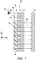
- FIG. 1 a block diagram shows an optical device using an LVCR 100 with an exit-pupil expander 102 according to an embodiment.
- the LCVR 100 includes a liquid-crystal layer 101 adjacent a substrate 103.
- the LCVR 100 is adjacent to a reference light source 104, such as a laser that provides collimated monochromatic light with a predetermined polarization state.
- a reference light source 104 such as a laser that provides collimated monochromatic light with a predetermined polarization state.
- Other light sources may be used, e.g., light-emitting diodes, and used with other optics integrated with the light source 104 or substrate, such as collimators, polarizers, filters, mode shifters, etc.
- Light from the light source 104 is coupled into the exit-pupil expander 102, which includes a glass substrate 108 that, as shown in this example, may be formed integrally with the LCVR 100.
- Light 105 (indicated by dashed lines in the figure) from the light source 104 is coupled into the glass substrate 108 via an optical input feature 106, such as an input waveguide, input facet, or diffractive optical element such as a ruled or holographic grating.
- the glass substrate functions as a waveguide that guides the light to a plurality of second coupling elements 110 that couple light 109 out of the substrate 108 and through the LCVR 100.
- the angular field-of-view of the expanded exit-pupil should be very small.
- a preferred embodiment would ensure that the coupled light 109 would have a nominally linear polarization state with a nominally 45 degree angle between the polarization axis and the slow axis of the LCVR 100.
- the plurality of coupling elements 110 are spatially dispersed over a major surface of the glass substrate 108.
- the major surface corresponds to an xy-plane.
- a detector 114 such as a focal-plane array (FPA) behind the LCVR 100, for example when used for hyperspectral imaging.
- FPA focal-plane array
- the detector 114 has corresponding sensors (e.g., pixels) at these locations, and a separate measurement of optical path delay can be made at each xy-coordinate, in a preferred embodiment by analyzing the intensity of light polarized parallel to the polarization of the coupled light 109.
- the coupling elements 110 cause light emitted from the exit-pupil expander 102 to be dispersed through one or more spatially unique regions of the LCVR 100.
- the one or more coupling elements 110 may be arranged such that the exit-pupil expander 102 emits light 109 in the z-direction and from a one-dimensional pattern, e.g., from a line parallel to the y-direction. In other embodiments, the exit-pupil expander 102 may emit a two-dimensional pattern.
- FIGS. 2 and 3 show examples of exit-pupil expanders that emit two-dimensional patterns and may be used in the apparatus of FIG. 1 .
- an exit-pupil expander includes a transparent substrate 200 with an optical input feature 202 (e.g., a diffractive grating, input waveguide, etc.) on a surface 200b of the substrate 200.
- the optical input 202 could be on any surface of the substrate 200, including the edges.
- the optical input 202 is configured to receive light from a light source 204 and direct the light along a first path 206, e.g., a first horizontal waveguide formed in the substrate 200.
- a plurality of first coupling elements 208 are configured to reflect a part of the light to second paths 210, e.g., second vertical waveguides formed in the substrate 200.
- a plurality of second coupling elements 212 are arranged along the second light paths 210 and configured to reflect part of light incident on the elements 212 towards an output surface 200a of the substrate 200.
- the second coupling elements 212 are shown arranged in a rectangular grid, although other patterns are possible.
- the coupling elements 212 can be non-evenly spatially distributed based on a priori knowledge of the LCVR, e.g., increasing density of the elements 212 in regions that are to experience larger spatial gradients of retardance.
- each of the coupling elements 208, 212 will be configured to reflect a first portion of light and transmit a second portion of light further along the light path.
- the leftmost optical element 208 would be configured to reflect 1/6 of the incident light in the negative y-direction and transmit 5/6 of the incident light in the x-direction.
- the next optical element would reflect 1/5 and pass 4/5, with each element reflecting a relatively greater portion until the rightmost element 208 reflects all of the light.
- an exit-pupil expander includes a transparent substrate 300 with two or more optical inputs 302 (e.g., diffractive gratings, input waveguides, etc.) on one or more surfaces.
- the optical inputs 302 are configured to receive light from two or more light sources 304 and direct the light along two or more paths 306, e.g., horizontal waveguides formed in the substrate 300.
- a plurality of coupling elements 308 are configured to reflect a part of the light out of an exit surface 300a of the substrate 300.
- the coupling elements 308 may be configured similarly to like-named elements described in relation to FIG. 2 .
- An optical device as shown in FIG. 1 can use an exit-pupil expander using any combinations of features shown in FIGS. 2 and 3 .
- the optical couplers in FIGS. 2 and 3 may use different types of optical elements to result in different patterns being formed at the exit-pupil.
- coupling elements can form lines, curves, and other shapes instead of the dots shown in FIGS. 2 and 3 .
- exit-pupil expanders may be formed using microlens arrays or micro-opto-electro-mechanical devices, and holographic optics may be used instead of or in addition to the partially-reflective and/or refractive elements shown above.
- FIG. 4 a diagram shows a polarization interferometer 400 that includes an optical device 401 according to an example embodiment.
- the optical device 401 includes an LCVR 402 and exit-pupil expander 404 similar to that described in relation to FIG. 1 .
- the exit-pupil expander 404 may be integral with or separate from the LCVR 402.
- a reference light source 406 e.g., laser
- the polarization interferometer 400 also includes polarizers 410, 412 on respective first and second sides of the polarization interferometer.
- Polarizer 412 is placed between the LCVR 402 and the detector 408, such that light coupled out of the exit-pupil expander 404 also travels through the polarizer 412. Light from the light source 406 may or may not travel through the polarizer 412 before being coupled into the exit-pupil expander 404, as indicated by alternate paths 407a-b.
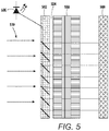
- FIG. 5 a diagram shows an LCVR 500 used with an exit-pupil expander 502 according to another example embodiment.
- the LCVR 500 and exit-pupil expander 502 are separated via a gap 504, e.g., an air gap.
- the gap 504 increases the index of refraction contrast between the waveguides in the exit-pupil expander 502 and the surrounding media.
- the liquid-crystal material within the LCVR 500 has a similar index of refraction to many of the transparent substrates used in LCVRs, e.g., glass, decreasing the number of guided optical modes within its substrates.
- a reference light source 506 and detector 508 can be used together with the LCVR 500 and exit-pupil expander 502.
- an exit-pupil expander does not adversely obscure the external light that is to pass through the LCVR, e.g., from an object to be imaged, as represented by arrows 510 in FIG. 5 .
- This can be done, for example, with the use of a "low efficiency" exit-pupil expander, e.g., using coupling elements that couple the light out of the guided modes of the exit-pupil expander with low efficiency.
- By optical reciprocity, such low-efficiency couplers would minimally couple the image light 510 into the guided modes of the exit-pupil expander 502 and would therefore allow the image light 510 to be imaged by the detector 508.
- the intensity of the light source 506 can always be increased to compensate for the low efficiency of the couplers.
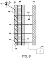
- a block diagram shows an exit-pupil expander 600 according to another example embodiment.
- the expander 600 provides an exit-pupil for a reference light source 602 to be expanded into a pattern across an LCVR 604, such as a pattern of dots or lines, that spatially samples the LCVR 604 with enough points to estimate the spatial distribution of retardance but not so many that it adversely obscures the LCVR's clear aperture.
- the exit-pupil expander 600 may include fewer and/or smaller optical coupling elements and waveguides than embodiments shown above.
- the optical coupling elements and waveguides may expand the area of the exit pupil to no more than 1% of a clear aperture of the LCVR 604.
- the clear aperture is an unobscured portion of the LCVR 604 through which light can pass, and for purposes of this disclosure, is intended to cover that unobscured portion of the LCVR 604 through which image light is passed.
- an optional feature 606 within the exit-pupil expander 600 can cause a portion 608 of the light that propagates through the exit-pupil expander 600 to rotate from linearly-polarized light to circularly-polarized, while the rest of the light 610 remains linearly polarized.
- the feature 606 may be a waveguide-based polarizing beam splitter followed by a 90° phase shifter of one polarization and a recombination of the two polarizations.
- the split light beams 608, 610 would couple into adjacent waveguides that travel through the exit-pupil expander 600, and are coupled out of the exit-pupil expander 600 using common or separate coupling elements 605 for each polarization.
- Each set of adjacent waveguides produces two separate arrays or patterns of dots or lines, the light from one array or pattern being polarization-rotated relative to the other.
- the separate arrays or patterns may be located in close proximity so that the in-phase and quadrature interferogram components can be measured as close to each other as possible via detector 615.
- the arrangement of beam-splitting and polarizing components should be such that the polarization states of split light beams 608, 610 should be as described, e.g., linear and circular polarization, upon exiting the exit-pupil expander.
- the feature 606 can be used in any of the embodiments described herein.
- two light sources e.g., two different light sources 304 as shown in FIG. 3
- the measurement using an exit-pupil expander is combined with one of an alternate modality that gives an absolute (though potentially not as accurate) measure of retardance.
- an alternate measurement is shown in FIG. 6 , where plates 612, 614 and processing circuitry 616 are used as a capacitance sensor.
- This sensor can detect capacitance between plates 612, 614 and across the liquid-crystal layer(s) 604 within the LCVR 604, which changes monotonically with retardance as taught in US Patent 5,247,378 dated September 21, 1993 .
- the capacitance may reflect an average retardance, and the spatially-dependent retardance found via the exit-pupil expander can be combined with the average retardance to find an absolute, spatially-dependent, accurate measure of the retardance of the LCVR 604.
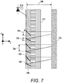
- FIG. 7 a block diagram shows an exit-pupil expander 700 that produces an interference pattern according to an example embodiment.
- Separate optical coupling elements 702, 704 couple light out of the expander 700 at different output angles 701, 703, e.g., relative to the z-axis in this example.
- interference patterns can be created on select regions of the detector 710.
- the distances 706, 708 and angles 701, 703 can be selected such that the rays exiting the LCVR 711 are directed to proximate but non-overlapping regions of the detector 710 such that no interference pattern is created.
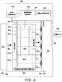
- FIG. 8 a block diagram illustrates an apparatus 800 according to an example embodiment.
- the apparatus 800 includes a device controller 802, which may include one or more processors, such as central processing units, subprocessors, digital signal processors, etc.
- the controller 802 is coupled to a memory 804 that includes functional modules that will be described in greater detail below.
- the memory 804 may include a combination of volatile and non-volatile memory, and may store instructions and data as known in the art.
- the apparatus includes an optical section 806 that includes an external optical interface 808 that receives light from outside the apparatus 800.
- the external optical interface 808 may include windows, lenses, filters, apertures, etc., suitable for passing light from outside the apparatus 800 to internal optical components.
- the external optical interface 808 is shown coupled to an external lens 810.
- a polarization interferometer 812 is located in the optical section 806 of the apparatus 800.
- the polarization interferometer 812 is coupled to the controller 802, e.g., via electrical signal lines.
- the controller 802 applies signals to the polarization interferometer 812 to cause a time-varying optical path delay or retardance in an LCVR 812a that is part of the interferometer 812.
- This time-varying optical path delay creates an interferogram that varies as a function of the optical path delay.
- the interferogram is detected by an image sensor 814 (e.g., an array of sensor pixels, focal plane array) which is also coupled to the controller 802.
- the polarization interferometer 812 includes LCVR 812a that may be configured similar to previously described embodiments. Between the external optical interface 808 and the LCVR 812a is an exit-pupil expander 812b.
- the exit-pupil expander 812b receives reference light 817a (e.g., polarized and/or collimated monochromatic light) from a light source 816 and expands the light across a major surface of the LCVR 812a.
- reference light 817a e.g., polarized and/or collimated monochromatic light
- a photodetector e.g., sensor 814 or optional separate detectors 815) on the other side of the interferometer 812 detects this expanded light 817b and produces a spatially-dependent photodetector signal, e.g., a signal that represents separate light intensity measurements each obtained at a plurality of locations on the detector 814, 815.
- the controller 802 extracts a spatially-dependent retardance measurement from the photodetector signal.
- the expanded reference light 817b may be detected together with or separate from other light 809 (e.g., from an image received from the lens 810) that passes through the LCVR 812a.
- the optical interface 808 may include a shutter that blocks incoming light for sufficient time to make measurements of the expanded light.
- the expanded reference light 817b could be time multiplexed with the image light 809. In such a case, the light source 816 is pulsed at a high intensity in conjunction with a very short exposure at the detector 814, 815. The high intensity of the expanded reference light 817b would minimize the influence of the image light 809.
- the intensity of the expanded reference light 817b were 100x or 10,000% of the intensity of the image light 809, then the very short exposure described above to measure the expanded reference light 817b could have an exposure time of 0.01x or 1% of the exposure time used to measure the image light 809 in order to produce the same time-integrated intensity. Therefore, the image light 809 would cause at most a 1% error in the measurement of the expanded reference light 817b.
- the intensity of the expanded reference light 817b could be adjusted to be similar to the image light 809 such that both could be simultaneously captured in the same exposure. If the expanded reference light 817b has sufficient intensity, it should cause a measurable spectral peak in the spectral data recovered via the detector 710, the peak corresponding to the known wavelength of the monochromatic light source 816. The difference between the measured peak wavelength and the known wavelength of the light source 816 could be used, for example, to calibrate the wavelength error of a hyperspectral imager as a function of image position.
- the spatially-dependent retardance measurement can be used by an image processor 820 to calculate a hyperspectral data-cube from recorded interferograms.
- the retardance controller 818 instructs the device controller 802 to apply a control signal to the LCVR 812a to achieve a time-varying retardance trajectory, generating spatially-dependent interferograms at the image sensor 814, also as a function of time.
- the image processor 820 can combine the spatially- and temporally-dependent retardance measurements and interferograms to first calculate the interferogram at each position as a function of retardance, and then to calculate the hyperspectral data-cube by Fourier-transforming all interferograms with respect to retardance.
- image processing may be performed by an external device, such as computer 824 that is coupled to the apparatus 800 via a data transfer interface 822.
- the computer 824 may also receive spatially-dependent retardance measurements obtained via the exit-pupil expander 812b.
- the retardance controller 818 can use the spatially-dependent retardance measured via the exit-pupil expander 812 and photodetector 814, 815 as an input to feedback or feedforward control models in order to cause the actual retardance to more closely follow the expected or desired retardance as a function of time.
- the spatially-dependent retardance measurements could be combined (e.g., spatially averaged) so that deviations from a desired target retardance trajectory can be detected and compensation provided, e.g., by adjusting electrical signals applied to the LCVR 812a.
- These control models could also utilize capacitance measurements of one or more of the LC cells within the LCVR 812a, e.g., as shown in FIG. 6 .
- the LCVR 812a may comprise more than one electrode (e.g., electrode pairs 812aa-812ac) on each substrate such that spatially-dependent control of the retardance is possible by independent control of the voltage signals across each electrode pair.
- the spatially-dependent retardance measurements in the vicinity of a single zone of control of the LCVR 812a would be averaged only over that zone and used to compensate the LCVR 812a control signals for only that zone.
- the use of the multiple electrode pairs 812aa-812ac can enable more precise retardance control of different regions of the LCVR 812a, which can reduce errors in the spectral data resulting from spatially-dependent retardance variation of the LCVR 812a. If the image light 809 passing through the LCVR 812a is focused by the lens 810 onto the image sensor 814 and the lens 810 has a large aperture-stop, then the rays of image light corresponding to one image sensor position will pass through different portions of the LCVR 812a and may therefore experience different retardances. This would reduce interferogram contrast and degrade the measurement of the spectral data in such a way that knowledge of the spatially-dependent retardance of the LCVR 812a would not be useful to compensate the degradation.
- the spatially-dependent retardance control enabled by the multiple electrode pairs 812aa-812ac could be used to increase the spatial homogeneity of the instantaneous retardance of the LCVR 812a in order to maintain high interferogram contrast and prevent this kind of measurement degradation.
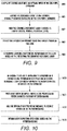
- FIG. 9 a flowchart shows a method according to an example embodiment.
- the method involves coupling 900 reference light into an optical input of an exit-pupil expander.
- the reference light is expanded 901 to one or more spatially-separated regions of the exit-pupil expander.
- the expanded reference light is passed 902 through an LCVR. Based on detecting 903 the expanded reference light that passes through the LCVR, a spatially-dependent retardance of the LCVR is determined 904.
- a flowchart shows a method according to another example embodiment.
- the method involves determining 1000 a spatially-dependent retardance of a polarization interferometer based on detecting reference light (e.g., monochromatic, coherent light) expanded through the interferometer by an exit-pupil expander.
- Light from an image is passed 1001 through the polarization interferometer to form interferograms.
- the spatially-dependent retardance of the LCVR is used 1002 to reduce errors in the interferograms, e.g., due to spatial variations of optical retardance of the LCVR.
- a hyperspectral data-cube may optionally be obtained 1003 based on the corrected interferograms.
Landscapes
- Physics & Mathematics (AREA)
- General Physics & Mathematics (AREA)
- Spectroscopy & Molecular Physics (AREA)
- Nonlinear Science (AREA)
- Optics & Photonics (AREA)
- Chemical & Material Sciences (AREA)
- Crystallography & Structural Chemistry (AREA)
- Mathematical Physics (AREA)
- Liquid Crystal (AREA)
- Optical Modulation, Optical Deflection, Nonlinear Optics, Optical Demodulation, Optical Logic Elements (AREA)
- Spectrometry And Color Measurement (AREA)
- Investigating Or Analysing Materials By Optical Means (AREA)
Abstract
Description
- The present disclosure is directed to an exit-pupil expander used to expand light over a liquid-crystal variable retarder. In one embodiment an optical device includes a liquid-crystal variable retarder. An exit-pupil expander is optically coupled to the liquid-crystal variable retarder, the exit-pupil expander includes: at least one optical input feature that receives reference light from a reference light source; and one or more optical coupling elements coupled to receive the reference light from the reference light source and expand the reference light to one or more spatially-separated regions of the liquid-crystal variable retarder.
- In another embodiment, reference light is coupled into an optical input of an exit-pupil expander. The reference light is expanded to one or more spatially-separated regions of the exit-pupil expander. The expanded reference light is passed through a liquid-crystal variable retarder. Based on detecting the expanded reference light that passes through the liquid-crystal variable retarder, a spatially-dependent retardance of the liquid-crystal variable retarder is determined.
- These and other features and aspects of various embodiments may be understood in view of the following detailed discussion and accompanying drawings.
- The discussion below makes reference to the following figures, wherein the same reference number may be used to identify the similar/same component in multiple figures. The drawings are not necessarily to scale.
-
FIG. 1 is a diagram of an optical device according to an example embodiment; -
FIGS. 2 and3 are diagrams of exit-pupil expanders according to example embodiments; -
FIG. 4 is a block diagram of a polarization interferometer according to an example embodiment; -
FIGS. 5-7 are diagram of liquid-crystal variable retarders according to other example embodiments; -
FIG. 8 is a block diagram of an apparatus according to another example embodiment; and -
FIGS. 9 and 10 are flowcharts of methods according to example embodiments. - The present disclosure relates to liquid-crystal devices used for optical retardance control. Generally, liquid-crystal (LC) materials are liquids having some crystalline properties (e.g., orientation of internal structures, such as the LC director that indicates the local average alignment of LC molecules) that can be selectably altered by applying an external stimulus, such as an electric field or a magnetic field. A change in orientation of the LC director alters the optical properties of the LC materials, e.g., changing the optical axis of the LC birefringence. While the selectable orientation of liquid crystals has a wide range of applications (e.g., electronic displays) the present disclosure is directed to a class of devices known as variable optical retarders, or LC variable retarders (LCVRs).
- An LCVR generates a variable optical path delay, or a variable retardance, between two orthogonal polarizations of light that travel through the liquid crystal. One or more liquid-crystal cells within the LCVR function as electrically tunable birefringent elements. By varying the voltage across the electrodes of the liquid-crystal cell, the cell molecules change their orientation, and it is possible to create a variable optical path delay between first rays in an incident polarization direction and second rays in an orthogonal polarization (e.g., ordinary and extraordinary rays). This path delay causes a wavelength-dependent phase shift between the first and second rays.
- Because LCVRs generate an electrically-controllable optical path delay, they are sometimes used within interferometers, specifically polarization interferometers. Polarization interferometers are common-path interferometers (meaning that both arms of the interferometer follow the same geometrical path) that combine polarizing elements with birefringent elements to generate interferograms, whereby the optical path delay induced by the birefringent elements varies spatially and/or temporally.
- To create a polarization interferometer with an LCVR, the LCVR is placed between a first polarizer and a second polarizer with nominally parallel or perpendicular polarization axes. The slow axis of the LCVR (the polarization axis with the variable optical path delay) is oriented nominally 45 degrees with respect to the polarization direction of the first polarizer. Incoming light is polarized to an incident polarization direction by the first polarizer. Because the slow axis of the LCVR is at 45 degrees with respect to this incident polarization direction, the polarized incident light can be described in terms of a portion of light polarized parallel to the slow axis of the LCVR and a portion of light polarized perpendicular to this axis.
- As the light passes through the LCVR, it acquires a wavelength-dependent relative phase shift between the first and second polarizations, thereby leading to a wavelength-dependent change in the polarization state. The second polarizer, or analyzer, oriented either parallel or perpendicular to the first polarizer, interferes the portion of light polarized parallel to the slow axis of the LCVR with the portion of light polarized perpendicular, changing the wavelength-dependent polarization state at the output of the LCVR into a wavelength-dependent intensity pattern that can be sensed by an optical detector or a focal plane array. By sensing this intensity while varying the retardance of the LCVR, it is possible to measure an interferogram of the incoming light, which can be used to ascertain spectral properties of the incoming light.
- A polarization interferometer based on an LCVR may have a number of uses. For example, such a device may be used in hyperspectral imaging applications because of its abilities to encode spectral information of the incident light into an intensity pattern that is easily measured with a non-spectrally-resolving detector. Hyperspectral imaging refers to methods and devices for acquiring hyperspectral datasets or data-cubes, which may include images where densely sampled, finely resolved spectral information is provided at each pixel.
- The wavelength-dependent intensity pattern provided by the polarization interferometer corresponds approximately to a cosine transform of the spectrum of the incident light. By recording the spatially-dependent intensity pattern at the output of a polarization interferometer as a function of the LCVR's retardance, the interferograms generated by all points of a scene imaged through the LCVR can be sampled simultaneously. From this, the hyperspectral data-cube can be nominally recovered by applying a transform, such as an inverse cosine transform or Fourier transform along the retardance axis, to the recorded spatially-dependent interferogram.
- To accurately calculate the hyperspectral data-cube, the processing apparatus used to apply the above transform should have precise knowledge of the optical path delay of the LCVR over its clear aperture for each individual interferogram sample. This can be done, for example, with a monochromatic reference light source, calibration light source, or laser that is pointed through the LCVR and linearly polarized at 45 degrees with respect to the LCVR's slow axis. The intensity of the light that has passed through the LCVR and is polarized parallel to the source polarization is recorded, and the phase (and thus the optical path delay) is calculated via methods known in the art, such as the Takeda Fourier-transform method. However, for practical reasons, this measurement is typically done only at one location of the LCVR, using the assumption that the retardance of the LCVR has no spatial dependence. However, the LCVR can have significant spatially-dependent retardance variation, so this assumption can lead to potential errors in calculating portions of the hyperspectral data-cube from regions of the spatially-dependent interferogram that are imaged through positions of the LCVR that differ substantially in retardance from where the retardance is actually measured.
- The LCVRs typically used for a hyperspectral imager generally comprise thick LC layers in order to access a high level of optical retardance. This required LC layer thickness leads to LCVRs that switch slowly, potentially much more slowly than is desirable in a hyperspectral imaging arrangement. It is possible to switch the LCVR much faster than its natural relaxation time by dynamically driving the LCVR with an appropriate voltage waveform. However, the faster the LCVR is driven, the more likely it is that a spatial dependence is introduced into the instantaneous retardance. This is because the LC cells in the LCVR are generally not perfectly flat or homogeneous, and each position responds differently depending on its thickness or other position-dependent parameters. In order to remedy this, the spatially-dependent retardance can be measured at many points across the LCVR as the nominal retardance is changed in order to improve accuracy of the transform operations used to calculate the hyperspectral data-cube. More details of the hyperspectral imaging process can be found in
U.S. Publication 2016/0123811, dated May 5, 2016 , as well as A. Hegyi and J. Martini, Opt. Express 23, 28742-28754 (2015). - One technique for combining two images in a compact form factor is referred to as "waveguiding." Generally, light from a display is coupled into a glass "waveguide" that forms the display window using some form of coupling element, e.g., a diffractive optical element. It is then coupled out of the display window using a second coupling element. The coupling element could be, for example, a diffractive element, partially reflective element, waveguide coupler, etc. This arrangement functions as a periscope, and it expands the exit-pupil of the display. It is known in the art as an "exit-pupil expander." The present disclosure relates to a device and a method for combining an exit-pupil expander with a liquid-crystal variable retarder.
- In
FIG. 1 , a block diagram shows an optical device using anLVCR 100 with an exit-pupil expander 102 according to an embodiment. The LCVR 100 includes a liquid-crystal layer 101 adjacent asubstrate 103. TheLCVR 100 is adjacent to areference light source 104, such as a laser that provides collimated monochromatic light with a predetermined polarization state. Other light sources may be used, e.g., light-emitting diodes, and used with other optics integrated with thelight source 104 or substrate, such as collimators, polarizers, filters, mode shifters, etc. Light from thelight source 104 is coupled into the exit-pupil expander 102, which includes aglass substrate 108 that, as shown in this example, may be formed integrally with theLCVR 100. Light 105 (indicated by dashed lines in the figure) from thelight source 104 is coupled into theglass substrate 108 via anoptical input feature 106, such as an input waveguide, input facet, or diffractive optical element such as a ruled or holographic grating. The glass substrate functions as a waveguide that guides the light to a plurality ofsecond coupling elements 110 that couple light 109 out of thesubstrate 108 and through theLCVR 100. In contrast to near-eye displays, the angular field-of-view of the expanded exit-pupil should be very small. This is so the angular dependence of the optical path delay through theLCVR 100 is not an issue. A preferred embodiment would ensure that the coupled light 109 would have a nominally linear polarization state with a nominally 45 degree angle between the polarization axis and the slow axis of theLCVR 100. - The plurality of
coupling elements 110 are spatially dispersed over a major surface of theglass substrate 108. In the illustrated example, the major surface corresponds to an xy-plane. There may be adetector 114, such as a focal-plane array (FPA) behind theLCVR 100, for example when used for hyperspectral imaging. The coupling of the light 105 to different regions of theLC layer 101 allows measuring instantaneous optical path delay at different xy-coordinates through theLCVR 100. Thedetector 114 has corresponding sensors (e.g., pixels) at these locations, and a separate measurement of optical path delay can be made at each xy-coordinate, in a preferred embodiment by analyzing the intensity of light polarized parallel to the polarization of the coupled light 109. - The
coupling elements 110 cause light emitted from the exit-pupil expander 102 to be dispersed through one or more spatially unique regions of theLCVR 100. The one ormore coupling elements 110 may be arranged such that the exit-pupil expander 102 emits light 109 in the z-direction and from a one-dimensional pattern, e.g., from a line parallel to the y-direction. In other embodiments, the exit-pupil expander 102 may emit a two-dimensional pattern. The diagrams ofFIGS. 2 and3 show examples of exit-pupil expanders that emit two-dimensional patterns and may be used in the apparatus ofFIG. 1 . - In
FIG. 2 , an exit-pupil expander includes atransparent substrate 200 with an optical input feature 202 (e.g., a diffractive grating, input waveguide, etc.) on a surface 200b of thesubstrate 200. Theoptical input 202 could be on any surface of thesubstrate 200, including the edges. Theoptical input 202 is configured to receive light from alight source 204 and direct the light along afirst path 206, e.g., a first horizontal waveguide formed in thesubstrate 200. A plurality offirst coupling elements 208 are configured to reflect a part of the light tosecond paths 210, e.g., second vertical waveguides formed in thesubstrate 200. It will be understood that the terms "horizontal" and "vertical" are used for convenience in reference to the drawings and not considered limiting; the exit-pupil expander will generally operate the same in any orientation. - A plurality of
second coupling elements 212 are arranged along the secondlight paths 210 and configured to reflect part of light incident on theelements 212 towards anoutput surface 200a of thesubstrate 200. Thesecond coupling elements 212 are shown arranged in a rectangular grid, although other patterns are possible. For example, thecoupling elements 212 can be non-evenly spatially distributed based on a priori knowledge of the LCVR, e.g., increasing density of theelements 212 in regions that are to experience larger spatial gradients of retardance. Note that each of thecoupling elements optical element 208 would be configured to reflect 1/6 of the incident light in the negative y-direction and transmit 5/6 of the incident light in the x-direction. The next optical element would reflect 1/5 and pass 4/5, with each element reflecting a relatively greater portion until therightmost element 208 reflects all of the light. These values can be adjusted for optical losses, manufacturing tolerances, a desired non-uniform intensity distribution, etc. - In
FIG. 3 , an exit-pupil expander includes atransparent substrate 300 with two or more optical inputs 302 (e.g., diffractive gratings, input waveguides, etc.) on one or more surfaces. Theoptical inputs 302 are configured to receive light from two or morelight sources 304 and direct the light along two ormore paths 306, e.g., horizontal waveguides formed in thesubstrate 300. A plurality ofcoupling elements 308 are configured to reflect a part of the light out of an exit surface 300a of thesubstrate 300. Thecoupling elements 308 may be configured similarly to like-named elements described in relation toFIG. 2 . - An optical device as shown in
FIG. 1 can use an exit-pupil expander using any combinations of features shown inFIGS. 2 and3 . Note that the optical couplers inFIGS. 2 and3 may use different types of optical elements to result in different patterns being formed at the exit-pupil. For example, coupling elements can form lines, curves, and other shapes instead of the dots shown inFIGS. 2 and3 . It should be mentioned that other methods of exit-pupil expansion can be used. For example, exit-pupil expanders may be formed using microlens arrays or micro-opto-electro-mechanical devices, and holographic optics may be used instead of or in addition to the partially-reflective and/or refractive elements shown above. - In
FIG. 4 , a diagram shows apolarization interferometer 400 that includes anoptical device 401 according to an example embodiment. Theoptical device 401 includes anLCVR 402 and exit-pupil expander 404 similar to that described in relation toFIG. 1 . The exit-pupil expander 404 may be integral with or separate from theLCVR 402. A reference light source 406 (e.g., laser) couples light into the exit-pupil expander 404, which directs it out of theLCVR 402 towards adetector 408. Thepolarization interferometer 400 also includespolarizers Polarizer 412 is placed between theLCVR 402 and thedetector 408, such that light coupled out of the exit-pupil expander 404 also travels through thepolarizer 412. Light from thelight source 406 may or may not travel through thepolarizer 412 before being coupled into the exit-pupil expander 404, as indicated byalternate paths 407a-b. - In
FIG. 5 , a diagram shows anLCVR 500 used with an exit-pupil expander 502 according to another example embodiment. TheLCVR 500 and exit-pupil expander 502 are separated via agap 504, e.g., an air gap. Thegap 504 increases the index of refraction contrast between the waveguides in the exit-pupil expander 502 and the surrounding media. The liquid-crystal material within theLCVR 500 has a similar index of refraction to many of the transparent substrates used in LCVRs, e.g., glass, decreasing the number of guided optical modes within its substrates. Therefore, in many embodiments it may be preferable to include thegap 504 in order to sufficiently maintain the desired guided optical modes within the waveguides of the exit-pupil expander 502. As with previous figures, areference light source 506 anddetector 508 can be used together with theLCVR 500 and exit-pupil expander 502. - Consideration should be made such that an exit-pupil expander does not adversely obscure the external light that is to pass through the LCVR, e.g., from an object to be imaged, as represented by
arrows 510 inFIG. 5 . This can be done, for example, with the use of a "low efficiency" exit-pupil expander, e.g., using coupling elements that couple the light out of the guided modes of the exit-pupil expander with low efficiency. By optical reciprocity, such low-efficiency couplers would minimally couple theimage light 510 into the guided modes of the exit-pupil expander 502 and would therefore allow theimage light 510 to be imaged by thedetector 508. The intensity of thelight source 506 can always be increased to compensate for the low efficiency of the couplers. - In
FIG. 6 , a block diagram shows an exit-pupil expander 600 according to another example embodiment. Theexpander 600 provides an exit-pupil for areference light source 602 to be expanded into a pattern across anLCVR 604, such as a pattern of dots or lines, that spatially samples theLCVR 604 with enough points to estimate the spatial distribution of retardance but not so many that it adversely obscures the LCVR's clear aperture. Thus, the exit-pupil expander 600 may include fewer and/or smaller optical coupling elements and waveguides than embodiments shown above. For example, the optical coupling elements and waveguides may expand the area of the exit pupil to no more than 1% of a clear aperture of theLCVR 604. Generally, the clear aperture is an unobscured portion of theLCVR 604 through which light can pass, and for purposes of this disclosure, is intended to cover that unobscured portion of theLCVR 604 through which image light is passed. - Note that, even with a coverage as small as 1% of the LCVR's clear aperture, the
exit pupil expander 600 can distribute reference light over enough spatially-distributed regions to estimate the spatially-dependent retardance to a high degree of accuracy. For example, consider a 30 mm x 20 mm (600 mm2) clear aperture of an LCVR that is divided into 600 squares (30 x 20 grid) in which retardance is to be separately measured. Further assume for this example that the exit-pupil expander distributes the reference light to a 30 x 20 grid of square output couplers, each approximately (0.1 mm)2 = 0.01 mm2 in area. In such a case, the total area of the output couplers would be 600 x 0.01 mm2, which is (6 mm2)/(600 mm2) = 1% of the total area of the clear aperture. Note that for simplicity we do not include in the above calculation the obscuration of the clear aperture by waveguides and coupling elements other than the output couplers, although their effects on the clear aperture can also be included. - In combination with or separate from the above, it may be useful to divide the laser light into two predefined polarization states, e.g., linear and circular polarization states, such that the in-phase and quadrature components of the interferograms used to sample each position of the retardance can be measured. These two measurements can be done using time-multiplexing or space-multiplexing. For example, as shown in
FIG. 6 , anoptional feature 606 within the exit-pupil expander 600 can cause aportion 608 of the light that propagates through the exit-pupil expander 600 to rotate from linearly-polarized light to circularly-polarized, while the rest of the light 610 remains linearly polarized. By comparing the instantaneous intensities from the interferograms of the linearly- and circularly-polarized reference light, or the in-phase and quadrature intensities, it is possible to calculate the instantaneous phase delay, modulo 2π, of the reference light through the LCVR. - The
feature 606 may be a waveguide-based polarizing beam splitter followed by a 90° phase shifter of one polarization and a recombination of the two polarizations. The split light beams 608, 610 would couple into adjacent waveguides that travel through the exit-pupil expander 600, and are coupled out of the exit-pupil expander 600 using common orseparate coupling elements 605 for each polarization. Each set of adjacent waveguides produces two separate arrays or patterns of dots or lines, the light from one array or pattern being polarization-rotated relative to the other. As seen in the figures, the separate arrays or patterns (or elements thereof) may be located in close proximity so that the in-phase and quadrature interferogram components can be measured as close to each other as possible viadetector 615. Note that the arrangement of beam-splitting and polarizing components should be such that the polarization states of splitlight beams - The
feature 606 can be used in any of the embodiments described herein. In other embodiments, two light sources (e.g., two differentlight sources 304 as shown inFIG. 3 ) can be configured such that light from the sources is coupled into the exit-pupil expander at different polarizations and distributed through the exit-pupil expander via separate waveguides. Again, this can be used with any of the embodiments described herein by introducing one or more additional light sources and input coupling elements and different waveguides within the exit-pupil expander. - Note that because the measurement of retardance described above relies on detecting the relative phase of two polarizations of light passing from the exit-pupil expander through the LCVR, and because phase can only be directly measured modulo 2π, there is an inherent ambiguity in the measurement of retardance. It some embodiments, the measurement using an exit-pupil expander is combined with one of an alternate modality that gives an absolute (though potentially not as accurate) measure of retardance. One example of such an alternate measurement is shown in
FIG. 6 , whereplates processing circuitry 616 are used as a capacitance sensor. This sensor can detect capacitance betweenplates LCVR 604, which changes monotonically with retardance as taught inUS Patent 5,247,378 dated September 21, 1993 . The capacitance may reflect an average retardance, and the spatially-dependent retardance found via the exit-pupil expander can be combined with the average retardance to find an absolute, spatially-dependent, accurate measure of the retardance of theLCVR 604. - In
FIG. 7 , a block diagram shows an exit-pupil expander 700 that produces an interference pattern according to an example embodiment. Separateoptical coupling elements expander 700 atdifferent output angles angles relative spacing 706 betweenelements distance 708 between theelements detector 710, interference patterns can be created on select regions of thedetector 710. In other embodiments, thedistances angles LCVR 711 are directed to proximate but non-overlapping regions of thedetector 710 such that no interference pattern is created. - In
FIG. 8 , a block diagram illustrates anapparatus 800 according to an example embodiment. Theapparatus 800 includes adevice controller 802, which may include one or more processors, such as central processing units, subprocessors, digital signal processors, etc. Thecontroller 802 is coupled to amemory 804 that includes functional modules that will be described in greater detail below. Thememory 804 may include a combination of volatile and non-volatile memory, and may store instructions and data as known in the art. - The apparatus includes an
optical section 806 that includes an externaloptical interface 808 that receives light from outside theapparatus 800. The externaloptical interface 808 may include windows, lenses, filters, apertures, etc., suitable for passing light from outside theapparatus 800 to internal optical components. In this example, the externaloptical interface 808 is shown coupled to anexternal lens 810. - A
polarization interferometer 812 is located in theoptical section 806 of theapparatus 800. Thepolarization interferometer 812 is coupled to thecontroller 802, e.g., via electrical signal lines. Thecontroller 802 applies signals to thepolarization interferometer 812 to cause a time-varying optical path delay or retardance in anLCVR 812a that is part of theinterferometer 812. This time-varying optical path delay creates an interferogram that varies as a function of the optical path delay. The interferogram is detected by an image sensor 814 (e.g., an array of sensor pixels, focal plane array) which is also coupled to thecontroller 802. - The
polarization interferometer 812 includesLCVR 812a that may be configured similar to previously described embodiments. Between the externaloptical interface 808 and theLCVR 812a is an exit-pupil expander 812b. The exit-pupil expander 812b receivesreference light 817a (e.g., polarized and/or collimated monochromatic light) from alight source 816 and expands the light across a major surface of theLCVR 812a. A photodetector (e.g.,sensor 814 or optional separate detectors 815) on the other side of theinterferometer 812 detects this expanded light 817b and produces a spatially-dependent photodetector signal, e.g., a signal that represents separate light intensity measurements each obtained at a plurality of locations on thedetector controller 802 extracts a spatially-dependent retardance measurement from the photodetector signal. - Note that the expanded
reference light 817b may be detected together with or separate from other light 809 (e.g., from an image received from the lens 810) that passes through theLCVR 812a. For example, theoptical interface 808 may include a shutter that blocks incoming light for sufficient time to make measurements of the expanded light. In other embodiments, the expandedreference light 817b could be time multiplexed with theimage light 809. In such a case, thelight source 816 is pulsed at a high intensity in conjunction with a very short exposure at thedetector reference light 817b would minimize the influence of theimage light 809. For example, if the intensity of the expandedreference light 817b were 100x or 10,000% of the intensity of theimage light 809, then the very short exposure described above to measure the expandedreference light 817b could have an exposure time of 0.01x or 1% of the exposure time used to measure theimage light 809 in order to produce the same time-integrated intensity. Therefore, theimage light 809 would cause at most a 1% error in the measurement of the expandedreference light 817b. - In other embodiments, the intensity of the expanded
reference light 817b could be adjusted to be similar to theimage light 809 such that both could be simultaneously captured in the same exposure. If the expandedreference light 817b has sufficient intensity, it should cause a measurable spectral peak in the spectral data recovered via thedetector 710, the peak corresponding to the known wavelength of the monochromaticlight source 816. The difference between the measured peak wavelength and the known wavelength of thelight source 816 could be used, for example, to calibrate the wavelength error of a hyperspectral imager as a function of image position. - The spatially-dependent retardance measurement, as a function of time, can be used by an
image processor 820 to calculate a hyperspectral data-cube from recorded interferograms. Generally, theretardance controller 818 instructs thedevice controller 802 to apply a control signal to theLCVR 812a to achieve a time-varying retardance trajectory, generating spatially-dependent interferograms at theimage sensor 814, also as a function of time. Theimage processor 820 can combine the spatially- and temporally-dependent retardance measurements and interferograms to first calculate the interferogram at each position as a function of retardance, and then to calculate the hyperspectral data-cube by Fourier-transforming all interferograms with respect to retardance. Some or all of this image processing may be performed by an external device, such ascomputer 824 that is coupled to theapparatus 800 via adata transfer interface 822. In such a case, thecomputer 824 may also receive spatially-dependent retardance measurements obtained via the exit-pupil expander 812b. - If there are errors in the expected-versus-actual retardance of the
LCVR 812a, there will be errors in the resulting spectral data or hyperspectral data-cube if the expected rather than actual retardance is used to calculate those data. Theretardance controller 818 can use the spatially-dependent retardance measured via the exit-pupil expander 812 andphotodetector LCVR 812a. These control models could also utilize capacitance measurements of one or more of the LC cells within theLCVR 812a, e.g., as shown inFIG. 6 . Alternatively, theLCVR 812a may comprise more than one electrode (e.g., electrode pairs 812aa-812ac) on each substrate such that spatially-dependent control of the retardance is possible by independent control of the voltage signals across each electrode pair. In this case, the spatially-dependent retardance measurements in the vicinity of a single zone of control of theLCVR 812a would be averaged only over that zone and used to compensate theLCVR 812a control signals for only that zone. - The use of the multiple electrode pairs 812aa-812ac can enable more precise retardance control of different regions of the
LCVR 812a, which can reduce errors in the spectral data resulting from spatially-dependent retardance variation of theLCVR 812a. If theimage light 809 passing through theLCVR 812a is focused by thelens 810 onto theimage sensor 814 and thelens 810 has a large aperture-stop, then the rays of image light corresponding to one image sensor position will pass through different portions of theLCVR 812a and may therefore experience different retardances. This would reduce interferogram contrast and degrade the measurement of the spectral data in such a way that knowledge of the spatially-dependent retardance of theLCVR 812a would not be useful to compensate the degradation. In this case, the spatially-dependent retardance control enabled by the multiple electrode pairs 812aa-812ac could be used to increase the spatial homogeneity of the instantaneous retardance of theLCVR 812a in order to maintain high interferogram contrast and prevent this kind of measurement degradation. - In
FIG. 9 , a flowchart shows a method according to an example embodiment. The method involves coupling 900 reference light into an optical input of an exit-pupil expander. The reference light is expanded 901 to one or more spatially-separated regions of the exit-pupil expander. The expanded reference light is passed 902 through an LCVR. Based on detecting 903 the expanded reference light that passes through the LCVR, a spatially-dependent retardance of the LCVR is determined 904. - In
FIG. 10 , a flowchart shows a method according to another example embodiment. The method involves determining 1000 a spatially-dependent retardance of a polarization interferometer based on detecting reference light (e.g., monochromatic, coherent light) expanded through the interferometer by an exit-pupil expander. Light from an image is passed 1001 through the polarization interferometer to form interferograms. The spatially-dependent retardance of the LCVR is used 1002 to reduce errors in the interferograms, e.g., due to spatial variations of optical retardance of the LCVR. A hyperspectral data-cube may optionally be obtained 1003 based on the corrected interferograms. - The various embodiments described above may be implemented using circuitry, firmware, and/or software modules that interact to provide particular results. One of skill in the relevant arts can readily implement such described functionality, either at a modular level or as a whole, using knowledge generally known in the art. For example, the flowcharts and control diagrams illustrated herein may be used to create computer-readable instructions/code for execution by a processor. Such instructions may be stored on a non-transitory computer-readable medium and transferred to the processor for execution as is known in the art. The structures and procedures shown above are only a representative example of embodiments that can be used to provide the functions described hereinabove.
- Unless otherwise indicated, all numbers expressing feature sizes, amounts, and physical properties used in the specification and claims are to be understood as being modified in all instances by the term "about." Accordingly, unless indicated to the contrary, the numerical parameters set forth in the foregoing specification and attached claims are approximations that can vary depending upon the desired properties sought to be obtained by those skilled in the art utilizing the teachings disclosed herein. The use of numerical ranges by endpoints includes all numbers within that range (e.g. 1 to 5 includes 1, 1.5, 2, 2.75, 3, 3.80, 4, and 5) and any range within that range.
- The foregoing description of the example embodiments has been presented for the purposes of illustration and description. It is not intended to be exhaustive or to limit the embodiments to the precise form disclosed. Many modifications and variations are possible in light of the above teaching. Any or all features of the disclosed embodiments can be applied individually or in any combination are not meant to be limiting, but purely illustrative. It is intended that the scope of the invention be limited not with this detailed description, but rather determined by the claims appended hereto.
Claims (10)
- An optical device comprising:a liquid-crystal variable retarder (LCVR);an exit-pupil expander optically coupled to the LCVR, the exit-pupil expander comprising:at least one optical input feature that receives reference light from a reference light source; andone or more optical coupling elements coupled to receive the reference light from the reference light source and expand the reference light to one or more spatially-separated regions of the LCVR.
- The optical device of claim 1, comprising a gap between the LCVR and the exit-pupil expander.
- The optical device of claim 1, wherein the exit-pupil expander is formed integrally with the LCVR.
- The device of claim 1, wherein at least one of the input feature and the optical coupling elements comprise a diffractive optical element.
- An apparatus comprising:a light source that provides reference light;an optical device comprising:a liquid-crystal variable retarder (LCVR);an exit-pupil expander optically coupled to the LCVR, the exit-pupil expander comprising:at least one optical input feature that receives the reference light from the light source; andone or more optical coupling elements coupled to receive the reference light from the light source and expand the reference light to one or more spatially-separated regions of the LCVR;a focal plane array arranged to detect the expanded reference light that passes through the LCVR and to generate electrical signals in response thereto; anda controller coupled to the focal plane array, the controller configured to determine a spatially-dependent retardance of the LCVR based on the electrical signals.
- The apparatus of claim 5, further comprising first and second polarizers on respective first and second sides of the optical device, the controller configured to apply a variable voltage across the LCVR to create a time-varying retardance affecting an image passing through the LCVR, the image passing through the polarizers and the LCVR forming interferograms detected via the focal plane array.
- The apparatus of claim 5, wherein the reference light comprises monochromatic, substantially collimated light.
- A method comprising:coupling reference light into an optical input of an exit-pupil expander;expanding the reference light to one or more spatially-separated regions of the exit-pupil expander;passing the expanded reference light through a liquid-crystal variable retarder (LCVR); andbased on detecting the expanded reference light that passes through the LCVR, determine a spatially-dependent retardance of the LCVR.
- The method of claim 8, wherein the LCVR and the exit-pupil expander are within a polarization interferometer, the method further comprising:passing an image through the polarization interferometer to form interferograms; andusing the spatially-dependent retardance of the LCVR to reduce errors in the interferograms.
- The method of claim 8, further comprising:determining an average retardance of the LCVR via a capacitance sensor; andcombining the spatially-dependent retardance with the average retardance to obtain an absolute, spatially-dependent retardance of the LCVR.
Applications Claiming Priority (1)
| Application Number | Priority Date | Filing Date | Title |
|---|---|---|---|
| US15/858,368 US10983338B2 (en) | 2017-12-29 | 2017-12-29 | Exit-pupil expander used distribute light over a liquid-crystal variable retarder |
Publications (1)
| Publication Number | Publication Date |
|---|---|
| EP3514482A1 true EP3514482A1 (en) | 2019-07-24 |
Family
ID=64901316
Family Applications (1)
| Application Number | Title | Priority Date | Filing Date |
|---|---|---|---|
| EP18212122.8A Pending EP3514482A1 (en) | 2017-12-29 | 2018-12-12 | Exit pupil expander used to distribute light over a liquid-crystal variable retarder |
Country Status (5)
| Country | Link |
|---|---|
| US (1) | US10983338B2 (en) |
| EP (1) | EP3514482A1 (en) |
| JP (1) | JP7021061B2 (en) |
| KR (1) | KR102418084B1 (en) |
| CN (1) | CN109991768B (en) |
Families Citing this family (3)
| Publication number | Priority date | Publication date | Assignee | Title |
|---|---|---|---|---|
| DE102019108677A1 (en) * | 2019-04-03 | 2020-10-08 | Carl Zeiss Jena Gmbh | Devices for generating light distributions with optical waveguides |
| DE102019108679A1 (en) | 2019-04-03 | 2020-10-08 | Carl Zeiss Ag | Devices for supplying energy to an active eye implant |
| DE102019108678A1 (en) | 2019-04-03 | 2020-10-08 | Carl Zeiss Ag | Device for supplying energy to an active eye implant |
Citations (3)
| Publication number | Priority date | Publication date | Assignee | Title |
|---|---|---|---|---|
| US5247378A (en) | 1991-06-07 | 1993-09-21 | Peter Miller | Optical retarder having means for determining the retardance of the cell corresponding to the sensed capacitance thereof |
| US20050036143A1 (en) * | 2003-08-15 | 2005-02-17 | Nanometrics Incorporated | Reference calibration of metrology instrument |
| US20160123811A1 (en) | 2014-10-29 | 2016-05-05 | Palo Alto Research Center Incorporated | Liquid crystal fourier transform imaging spectrometer |
Family Cites Families (84)
| Publication number | Priority date | Publication date | Assignee | Title |
|---|---|---|---|---|
| US4342516A (en) | 1980-03-07 | 1982-08-03 | The Perkin-Elmer Corporation | Filter indexing for spectrophotometer system |
| US4461543A (en) | 1982-03-26 | 1984-07-24 | Sperry Corporation | Electro optic switch |
| JPS62103529A (en) | 1985-10-31 | 1987-05-14 | Toshiba Corp | Composite pipe |
| US4848877A (en) | 1987-09-29 | 1989-07-18 | Cambridge Research And Instrumentation, Inc. | Liquid crystal devices and systems using such devices |
| US4905169A (en) | 1988-06-02 | 1990-02-27 | The United States Of America As Represented By The United States Department Of Energy | Method and apparatus for simultaneously measuring a plurality of spectral wavelengths present in electromagnetic radiation |
| US5126869A (en) | 1990-12-03 | 1992-06-30 | Raytheon Company | Two-dimensional, phased-array optical beam steerer |
| US5784162A (en) | 1993-08-18 | 1998-07-21 | Applied Spectral Imaging Ltd. | Spectral bio-imaging methods for biological research, medical diagnostics and therapy |
| DE69226998T2 (en) | 1991-07-19 | 1999-04-15 | Sharp K.K., Osaka | Optical modulation element and devices with such an element |
| US5347382A (en) | 1992-04-23 | 1994-09-13 | Rumbaugh Scott H | Liquid crystal cell retarder with driving beyond retardance value and two cells for high speed |
| JP2925064B2 (en) | 1993-12-02 | 1999-07-26 | 矢崎総業株式会社 | Tunable wavelength filter |
| JPH07212639A (en) | 1994-01-25 | 1995-08-11 | Sony Corp | Electronic shutter device for television and camera |
| US5751384A (en) | 1995-05-23 | 1998-05-12 | The Board Of Regents Of The University Of Colorado | Color polarizers for polarizing an additive color spectrum along a first axis and it's compliment along a second axis |
| US5856842A (en) | 1996-08-26 | 1999-01-05 | Kaiser Optical Systems Corporation | Apparatus facilitating eye-contact video communications |
| US5841536A (en) * | 1997-08-01 | 1998-11-24 | The United States Of America As Represented By The Director Of The National Security Agency | Polarization interferometer apparatus using the polarization dependent phase lag in a birefringent retarder |
| CN1299472A (en) | 1998-04-08 | 2001-06-13 | 科英应用技术公司 | High speed electro-optic modulator |
| US6373607B1 (en) * | 1998-05-22 | 2002-04-16 | Trex Communications Corporation | Liquid crystal variable retarder for free-space laser communication system |
| US6169594B1 (en) | 1998-08-24 | 2001-01-02 | Physical Optics Corporation | Beam deflector and scanner |
| US6421131B1 (en) | 1999-07-02 | 2002-07-16 | Cambridge Research & Instrumentation Inc. | Birefringent interferometer |
| GB2354833A (en) | 1999-09-28 | 2001-04-04 | Sharp Lab Of Europ Ltd | Liquid crystal device |
| US7116370B1 (en) | 2000-03-31 | 2006-10-03 | Sharp Laboratories Of Ameria, Inc. | Image processing system optical shifting mechanism |
| US6373614B1 (en) | 2000-08-31 | 2002-04-16 | Cambridge Research Instrumentation Inc. | High performance polarization controller and polarization sensor |
| US7973936B2 (en) | 2001-01-30 | 2011-07-05 | Board Of Trustees Of Michigan State University | Control system and apparatus for use with ultra-fast laser |
| US6576886B1 (en) | 2001-02-20 | 2003-06-10 | General Photonics Corporation | Dynamic control of polarization of an optical signal |
| JP4382317B2 (en) | 2001-12-06 | 2009-12-09 | シチズンホールディングス株式会社 | Liquid crystal variable wavelength filter device |
| US6744509B2 (en) | 2002-08-20 | 2004-06-01 | Meadowlark Optics, Inc. | Retardance sweep polarimeter and method |
| US7067795B1 (en) | 2002-10-03 | 2006-06-27 | General Photonics Corporation | Methods and systems for dynamic control of polarization of an optical signal |
| EP1411333B1 (en) | 2002-10-15 | 2006-03-08 | Centre National De La Recherche Scientifique (Cnrs) | A liquid crystal based polarimetric system, a process for its calibration, and a polarimetric measurement process |
| US20040129867A1 (en) * | 2002-12-20 | 2004-07-08 | Mackey Jeffrey R. | Force measurement system using polarization-state modulated optical polarimetry |
| US7897406B2 (en) | 2002-12-20 | 2011-03-01 | Fiso Technologies Inc. | Method and sensor for detecting a chemical substance using an optically anisotropic material |
| US7782377B2 (en) | 2003-02-26 | 2010-08-24 | Canon Kabushiki Kaisha | Image sensing apparatus, control method therefor, storage medium, and program to create correction data |
| JP4285350B2 (en) | 2004-02-26 | 2009-06-24 | セイコーエプソン株式会社 | Viewing angle control element and manufacturing method thereof, liquid crystal display device, electronic device |
| JP2005348140A (en) | 2004-06-03 | 2005-12-15 | Matsushita Electric Ind Co Ltd | Camera device |
| JP4400448B2 (en) | 2004-12-22 | 2010-01-20 | コニカミノルタセンシング株式会社 | Spectral luminance meter calibration method and calibration system operation program |
| US6992809B1 (en) | 2005-02-02 | 2006-01-31 | Chemimage Corporation | Multi-conjugate liquid crystal tunable filter |
| WO2006103663A1 (en) | 2005-03-29 | 2006-10-05 | Yoel Arieli | Spectral imaging camera and applications |
| US7420663B2 (en) | 2005-05-24 | 2008-09-02 | Bwt Property Inc. | Spectroscopic sensor on mobile phone |
| JP4684771B2 (en) | 2005-06-30 | 2011-05-18 | Hoya株式会社 | Image blur correction device |
| JP4205704B2 (en) | 2005-08-02 | 2009-01-07 | 国立大学法人 北海道大学 | Imaging polarization measurement method |
| US7639363B2 (en) | 2005-09-07 | 2009-12-29 | California Institute Of Technology | Electro-optic imaging Fourier transform spectrometer |
| US7630022B1 (en) | 2005-09-20 | 2009-12-08 | Thomas Baur | Advanced liquid crystal tunable filters and method |
| WO2007038410A2 (en) | 2005-09-27 | 2007-04-05 | Chemimage Corporation | Liquid crystal filter with tunable rejection band |
| US7525712B2 (en) | 2005-09-29 | 2009-04-28 | Teledyne Scientific & Imaging, Llc | Broad spectral range polarization rotator |
| DE102005048240A1 (en) | 2005-10-07 | 2007-04-19 | Stefan Steib | Method for the spectral, integrated calibration of an image sensor by means of monochromatic light sources |
| EP1952106B1 (en) | 2005-11-04 | 2014-08-27 | George Themelis | System for multispectral imaging |
| US8644911B1 (en) | 2006-06-30 | 2014-02-04 | Hypermed Imaging, Inc. | OxyVu-1 hyperspectral tissue oxygenation (HTO) measurement system |
| US8447087B2 (en) | 2006-09-12 | 2013-05-21 | Carestream Health, Inc. | Apparatus and method for caries detection |
| WO2008068753A2 (en) | 2006-12-04 | 2008-06-12 | Ben-Gurion University Of The Negev - Research And Development Authority | Polarization independent birefringent tunable filters |
| WO2008151155A2 (en) * | 2007-05-31 | 2008-12-11 | Board Of Regents, The University Of Texas System | Polarization-sensitive spectral interferometry |
| GB0717967D0 (en) | 2007-09-14 | 2007-10-24 | Cascade Technologies Ltd | Polarimetric hyperspectral imager |
| EP2265936A2 (en) | 2008-04-01 | 2010-12-29 | Koninklijke Philips Electronics N.V. | Spectral detector calibration |
| US8406859B2 (en) | 2008-08-10 | 2013-03-26 | Board Of Regents, The University Of Texas System | Digital light processing hyperspectral imaging apparatus |
| FR2937732B1 (en) | 2008-10-29 | 2010-12-31 | Horiba Jobin Yvon Sas | DEVICE AND METHOD FOR SPECTROSCOPIC POLARIMETRIC MEASUREMENTS IN THE VISIBLE AND NEAR INFRARED DOMAIN |
| WO2010081116A2 (en) | 2009-01-10 | 2010-07-15 | Goldfinch Solutions, Llc | System and method for analyzing properties of meat using multispectral imaging |
| US8525970B2 (en) | 2009-05-21 | 2013-09-03 | The Hong Kong University Of Science And Technology | Photo-aligned liquid-crystal micropolarimeter array and its manufacturing method |
| US8982313B2 (en) | 2009-07-31 | 2015-03-17 | North Carolina State University | Beam steering devices including stacked liquid crystal polarization gratings and related methods of operation |
| US7999933B2 (en) | 2009-08-14 | 2011-08-16 | Princeton Instruments | Method for calibrating imaging spectrographs |
| US8400574B2 (en) | 2010-04-16 | 2013-03-19 | Chemimage Corporation | Short wave infrared multi-conjugate liquid crystal tunable filter |
| US9111501B2 (en) | 2010-04-19 | 2015-08-18 | Sharp Kabushiki Kaisha | Display device |
| US20110299089A1 (en) | 2010-06-04 | 2011-12-08 | University Of Washington | Compact liquid crystal based fourier transform spectrometer system |
| US20120013922A1 (en) | 2010-07-19 | 2012-01-19 | Lotz Michael G | Print Data Format Modification Mechanism |
| US9046422B2 (en) | 2011-04-20 | 2015-06-02 | The Arizona Board Of Regents On Behalf Of The University Of Arizona | Ultra-compact snapshot imaging fourier transform spectrometer |
| US8422119B1 (en) | 2010-09-20 | 2013-04-16 | Disco Corporation | Compensation of beam walkoff in nonlinear crystal using cylindrical lens |
| US8736777B2 (en) | 2011-01-19 | 2014-05-27 | Chemimage Technologies Llc | VIS-SNIR multi-conjugate liquid crystal tunable filter |
| EP2551635A1 (en) | 2011-07-26 | 2013-01-30 | Hexagon Technology Center GmbH | Optical measurement system with filter unit for extracting electromagnetic radiation |
| JP6073883B2 (en) | 2011-07-28 | 2017-02-01 | マサチューセッツ インスティテュート オブ テクノロジー | Configuration of camera for 3D imaging of internal space |
| JP2013096883A (en) | 2011-11-02 | 2013-05-20 | Seiko Epson Corp | Spectroscopic measuring apparatus |
| CN102721470A (en) * | 2012-06-30 | 2012-10-10 | 青岛市光电工程技术研究院 | Static spectrum polarization imaging device |
| US20140362331A1 (en) | 2013-03-15 | 2014-12-11 | Chemlmage Corporation | Short-Wavelength Infrared (SWIR) Multi-Conjugate Liquid Crystal Tunable Filter |
| US20140354868A1 (en) | 2013-06-04 | 2014-12-04 | Corning Incorporated | Portable hyperspectral imager |
| US9513166B2 (en) | 2013-07-16 | 2016-12-06 | Utah State University Research Foundation | Split field spectral imager |
| JP5866577B2 (en) | 2013-07-29 | 2016-02-17 | パナソニックIpマネジメント株式会社 | Optical filter and polarization imaging apparatus using the same |
| US9631973B2 (en) | 2013-12-13 | 2017-04-25 | Raytheon Company | Multifunction imager |
| EP3126904B1 (en) | 2014-04-02 | 2018-11-28 | Essilor International | Achromatic phase modulator and optical device |
| US11490037B2 (en) | 2014-10-29 | 2022-11-01 | Palo Alto Research Center Incorporated | Liquid crystal fourier transform imaging spectrometer |
| US10469771B2 (en) | 2014-10-29 | 2019-11-05 | Palo Alto Research Center Incorporated | Liquid crystal fourier transform imaging spectrometer |
| EP3218669B1 (en) | 2014-11-16 | 2024-02-28 | ABDULHALIM, Ibrahim | Multi-spectral polarimetric variable optical device and imager |
| CN107430309B (en) | 2015-01-09 | 2020-11-06 | 依视路国际公司 | Liquid Crystal Achromatic Phase Modulator |
| US9535253B2 (en) * | 2015-02-09 | 2017-01-03 | Microsoft Technology Licensing, Llc | Display system |
| US10228517B2 (en) | 2015-03-03 | 2019-03-12 | Nistica, Inc. | Optical arrangement for managing diversity and isolation between ports in a wavelength selective switch |
| US10425598B2 (en) | 2016-06-20 | 2019-09-24 | Massachusetts Institute Of Technology | Methods and systems for time-encoded multiplexed imaging |
| CN112987303A (en) * | 2016-09-21 | 2021-06-18 | 奇跃公司 | System and method for optical system with exit pupil expander |
| US10768497B2 (en) | 2016-10-03 | 2020-09-08 | Xerox Corporation | Hyperspectral imaging system |
| JP2020514797A (en) | 2017-01-06 | 2020-05-21 | ニスティカ,インコーポレーテッド | Optical arrangement for suppressing out-of-band crosstalk in wavelength selective switches |
| US10884278B2 (en) | 2017-10-24 | 2021-01-05 | Palo Alto Research Center Incorporated | Liquid crystal temperature control by resistive heating |
-
2017
- 2017-12-29 US US15/858,368 patent/US10983338B2/en active Active
-
2018
- 2018-12-03 CN CN201811465061.XA patent/CN109991768B/en active Active
- 2018-12-06 JP JP2018228984A patent/JP7021061B2/en active Active
- 2018-12-12 EP EP18212122.8A patent/EP3514482A1/en active Pending
- 2018-12-14 KR KR1020180161742A patent/KR102418084B1/en active Active
Patent Citations (3)
| Publication number | Priority date | Publication date | Assignee | Title |
|---|---|---|---|---|
| US5247378A (en) | 1991-06-07 | 1993-09-21 | Peter Miller | Optical retarder having means for determining the retardance of the cell corresponding to the sensed capacitance thereof |
| US20050036143A1 (en) * | 2003-08-15 | 2005-02-17 | Nanometrics Incorporated | Reference calibration of metrology instrument |
| US20160123811A1 (en) | 2014-10-29 | 2016-05-05 | Palo Alto Research Center Incorporated | Liquid crystal fourier transform imaging spectrometer |
Non-Patent Citations (1)
| Title |
|---|
| J. MARTINI, OPT. EXPRESS, vol. 23, 2015, pages 28742 - 28754 |
Also Published As
| Publication number | Publication date |
|---|---|
| US20190204594A1 (en) | 2019-07-04 |
| KR102418084B1 (en) | 2022-07-07 |
| JP2019120931A (en) | 2019-07-22 |
| US10983338B2 (en) | 2021-04-20 |
| KR20190082092A (en) | 2019-07-09 |
| CN109991768A (en) | 2019-07-09 |
| JP7021061B2 (en) | 2022-02-16 |
| CN109991768B (en) | 2023-11-21 |
Similar Documents
| Publication | Publication Date | Title |
|---|---|---|
| US9739702B2 (en) | Symmetric target design in scatterometry overlay metrology | |
| US6469788B2 (en) | Coherent gradient sensing ellipsometer | |
| JP6702689B2 (en) | Liquid crystal Fourier transform imaging spectrometer | |
| CN103822712B (en) | Imaging method and imaging spectrometer based on Wollaston prism light splitting | |
| KR101544968B1 (en) | Thickness Measuring Apparatus and Thickness Measuring Method | |
| JP6553967B2 (en) | Instantaneous phase shift interferometer | |
| JP7340555B2 (en) | Methods for imaging or spectroscopy using nonlinear interferometry | |
| KR20100134609A (en) | Apparatus and method for measuring the surface shape of an object | |
| US10564504B2 (en) | Liquid-crystal variable retarder using liquid crystal cells of differing thicknesses | |
| JP2018059913A (en) | Hyperspectral Imaging System | |
| KR102418084B1 (en) | Exit-pupil expander used distribute light over a liquid-crystal variable retarder | |
| KR102007004B1 (en) | Apparatus for measuring three dimensional shape | |
| US6496269B2 (en) | Shape measuring apparatus | |
| JP2012013574A (en) | Optical type measurement device and prism for interferometer of the same | |
| JP3714854B2 (en) | Planar shape measuring method in phase shift interference fringe simultaneous imaging device | |
| JP2006329975A (en) | Interferometer and interferometer calibration method | |
| US8976360B2 (en) | Surface plasmon sensor and method of measuring refractive index | |
| JPWO2017159869A1 (en) | Electromagnetic field imaging device | |
| JP3714853B2 (en) | Planar shape measuring method in phase shift interference fringe simultaneous imaging device | |
| CN112219096A (en) | Method and system for measuring optical shear of a birefringent device beyond the diffraction limit | |
| JP7819056B2 (en) | Shape measuring device | |
| TW201420993A (en) | Multi-function measurement system for thin film elements | |
| KR102130576B1 (en) | Thickness And Refractive Index Measuring Apparatus Without Non-measuring Ranges | |
| NL1024070C2 (en) | Method and device for aligning an interferometer. | |
| CN118215834A (en) | Method and system for measuring optical properties of an object |
Legal Events
| Date | Code | Title | Description |
|---|---|---|---|
| PUAI | Public reference made under article 153(3) epc to a published international application that has entered the european phase |
Free format text: ORIGINAL CODE: 0009012 |
|
| STAA | Information on the status of an ep patent application or granted ep patent |
Free format text: STATUS: THE APPLICATION HAS BEEN PUBLISHED |
|
| AK | Designated contracting states |
Kind code of ref document: A1 Designated state(s): AL AT BE BG CH CY CZ DE DK EE ES FI FR GB GR HR HU IE IS IT LI LT LU LV MC MK MT NL NO PL PT RO RS SE SI SK SM TR |
|
| AX | Request for extension of the european patent |
Extension state: BA ME |
|
| STAA | Information on the status of an ep patent application or granted ep patent |
Free format text: STATUS: REQUEST FOR EXAMINATION WAS MADE |
|
| 17P | Request for examination filed |
Effective date: 20200124 |
|
| RBV | Designated contracting states (corrected) |
Designated state(s): AL AT BE BG CH CY CZ DE DK EE ES FI FR GB GR HR HU IE IS IT LI LT LU LV MC MK MT NL NO PL PT RO RS SE SI SK SM TR |
|
| STAA | Information on the status of an ep patent application or granted ep patent |
Free format text: STATUS: EXAMINATION IS IN PROGRESS |
|
| 17Q | First examination report despatched |
Effective date: 20211015 |