EP3514255A1 - Silicon coating on hard shields - Google Patents
Silicon coating on hard shields Download PDFInfo
- Publication number
- EP3514255A1 EP3514255A1 EP19152560.9A EP19152560A EP3514255A1 EP 3514255 A1 EP3514255 A1 EP 3514255A1 EP 19152560 A EP19152560 A EP 19152560A EP 3514255 A1 EP3514255 A1 EP 3514255A1
- Authority
- EP
- European Patent Office
- Prior art keywords
- layer
- thickness
- silicon layer
- spray process
- shield material
- Prior art date
- Legal status (The legal status is an assumption and is not a legal conclusion. Google has not performed a legal analysis and makes no representation as to the accuracy of the status listed.)
- Pending
Links
Images


Classifications
-
- C—CHEMISTRY; METALLURGY
- C23—COATING METALLIC MATERIAL; COATING MATERIAL WITH METALLIC MATERIAL; CHEMICAL SURFACE TREATMENT; DIFFUSION TREATMENT OF METALLIC MATERIAL; COATING BY VACUUM EVAPORATION, BY SPUTTERING, BY ION IMPLANTATION OR BY CHEMICAL VAPOUR DEPOSITION, IN GENERAL; INHIBITING CORROSION OF METALLIC MATERIAL OR INCRUSTATION IN GENERAL
- C23C—COATING METALLIC MATERIAL; COATING MATERIAL WITH METALLIC MATERIAL; SURFACE TREATMENT OF METALLIC MATERIAL BY DIFFUSION INTO THE SURFACE, BY CHEMICAL CONVERSION OR SUBSTITUTION; COATING BY VACUUM EVAPORATION, BY SPUTTERING, BY ION IMPLANTATION OR BY CHEMICAL VAPOUR DEPOSITION, IN GENERAL
- C23C28/00—Coating for obtaining at least two superposed coatings either by methods not provided for in a single one of groups C23C2/00 - C23C26/00 or by combinations of methods provided for in subclasses C23C and C25C or C25D
- C23C28/30—Coatings combining at least one metallic layer and at least one inorganic non-metallic layer
- C23C28/34—Coatings combining at least one metallic layer and at least one inorganic non-metallic layer including at least one inorganic non-metallic material layer, e.g. metal carbide, nitride, boride, silicide layer and their mixtures, enamels, phosphates and sulphates
-
- C—CHEMISTRY; METALLURGY
- C23—COATING METALLIC MATERIAL; COATING MATERIAL WITH METALLIC MATERIAL; CHEMICAL SURFACE TREATMENT; DIFFUSION TREATMENT OF METALLIC MATERIAL; COATING BY VACUUM EVAPORATION, BY SPUTTERING, BY ION IMPLANTATION OR BY CHEMICAL VAPOUR DEPOSITION, IN GENERAL; INHIBITING CORROSION OF METALLIC MATERIAL OR INCRUSTATION IN GENERAL
- C23C—COATING METALLIC MATERIAL; COATING MATERIAL WITH METALLIC MATERIAL; SURFACE TREATMENT OF METALLIC MATERIAL BY DIFFUSION INTO THE SURFACE, BY CHEMICAL CONVERSION OR SUBSTITUTION; COATING BY VACUUM EVAPORATION, BY SPUTTERING, BY ION IMPLANTATION OR BY CHEMICAL VAPOUR DEPOSITION, IN GENERAL
- C23C4/00—Coating by spraying the coating material in the molten state, e.g. by flame, plasma or electric discharge
- C23C4/04—Coating by spraying the coating material in the molten state, e.g. by flame, plasma or electric discharge characterised by the coating material
- C23C4/06—Metallic material
-
- B—PERFORMING OPERATIONS; TRANSPORTING
- B32—LAYERED PRODUCTS
- B32B—LAYERED PRODUCTS, i.e. PRODUCTS BUILT-UP OF STRATA OF FLAT OR NON-FLAT, e.g. CELLULAR OR HONEYCOMB, FORM
- B32B15/00—Layered products comprising a layer of metal
- B32B15/01—Layered products comprising a layer of metal all layers being exclusively metallic
- B32B15/012—Layered products comprising a layer of metal all layers being exclusively metallic one layer being formed of an iron alloy or steel, another layer being formed of aluminium or an aluminium alloy
-
- B—PERFORMING OPERATIONS; TRANSPORTING
- B32—LAYERED PRODUCTS
- B32B—LAYERED PRODUCTS, i.e. PRODUCTS BUILT-UP OF STRATA OF FLAT OR NON-FLAT, e.g. CELLULAR OR HONEYCOMB, FORM
- B32B15/00—Layered products comprising a layer of metal
- B32B15/01—Layered products comprising a layer of metal all layers being exclusively metallic
- B32B15/013—Layered products comprising a layer of metal all layers being exclusively metallic one layer being formed of an iron alloy or steel, another layer being formed of a metal other than iron or aluminium
-
- B—PERFORMING OPERATIONS; TRANSPORTING
- B32—LAYERED PRODUCTS
- B32B—LAYERED PRODUCTS, i.e. PRODUCTS BUILT-UP OF STRATA OF FLAT OR NON-FLAT, e.g. CELLULAR OR HONEYCOMB, FORM
- B32B15/00—Layered products comprising a layer of metal
- B32B15/01—Layered products comprising a layer of metal all layers being exclusively metallic
- B32B15/013—Layered products comprising a layer of metal all layers being exclusively metallic one layer being formed of an iron alloy or steel, another layer being formed of a metal other than iron or aluminium
- B32B15/015—Layered products comprising a layer of metal all layers being exclusively metallic one layer being formed of an iron alloy or steel, another layer being formed of a metal other than iron or aluminium the said other metal being copper or nickel or an alloy thereof
-
- B—PERFORMING OPERATIONS; TRANSPORTING
- B32—LAYERED PRODUCTS
- B32B—LAYERED PRODUCTS, i.e. PRODUCTS BUILT-UP OF STRATA OF FLAT OR NON-FLAT, e.g. CELLULAR OR HONEYCOMB, FORM
- B32B15/00—Layered products comprising a layer of metal
- B32B15/04—Layered products comprising a layer of metal comprising metal as the main or only constituent of a layer, which is next to another layer of the same or of a different material
-
- B—PERFORMING OPERATIONS; TRANSPORTING
- B32—LAYERED PRODUCTS
- B32B—LAYERED PRODUCTS, i.e. PRODUCTS BUILT-UP OF STRATA OF FLAT OR NON-FLAT, e.g. CELLULAR OR HONEYCOMB, FORM
- B32B15/00—Layered products comprising a layer of metal
- B32B15/04—Layered products comprising a layer of metal comprising metal as the main or only constituent of a layer, which is next to another layer of the same or of a different material
- B32B15/043—Layered products comprising a layer of metal comprising metal as the main or only constituent of a layer, which is next to another layer of the same or of a different material of metal
-
- B—PERFORMING OPERATIONS; TRANSPORTING
- B32—LAYERED PRODUCTS
- B32B—LAYERED PRODUCTS, i.e. PRODUCTS BUILT-UP OF STRATA OF FLAT OR NON-FLAT, e.g. CELLULAR OR HONEYCOMB, FORM
- B32B15/00—Layered products comprising a layer of metal
- B32B15/18—Layered products comprising a layer of metal comprising iron or steel
-
- B—PERFORMING OPERATIONS; TRANSPORTING
- B32—LAYERED PRODUCTS
- B32B—LAYERED PRODUCTS, i.e. PRODUCTS BUILT-UP OF STRATA OF FLAT OR NON-FLAT, e.g. CELLULAR OR HONEYCOMB, FORM
- B32B15/00—Layered products comprising a layer of metal
- B32B15/20—Layered products comprising a layer of metal comprising aluminium or copper
-
- C—CHEMISTRY; METALLURGY
- C23—COATING METALLIC MATERIAL; COATING MATERIAL WITH METALLIC MATERIAL; CHEMICAL SURFACE TREATMENT; DIFFUSION TREATMENT OF METALLIC MATERIAL; COATING BY VACUUM EVAPORATION, BY SPUTTERING, BY ION IMPLANTATION OR BY CHEMICAL VAPOUR DEPOSITION, IN GENERAL; INHIBITING CORROSION OF METALLIC MATERIAL OR INCRUSTATION IN GENERAL
- C23C—COATING METALLIC MATERIAL; COATING MATERIAL WITH METALLIC MATERIAL; SURFACE TREATMENT OF METALLIC MATERIAL BY DIFFUSION INTO THE SURFACE, BY CHEMICAL CONVERSION OR SUBSTITUTION; COATING BY VACUUM EVAPORATION, BY SPUTTERING, BY ION IMPLANTATION OR BY CHEMICAL VAPOUR DEPOSITION, IN GENERAL
- C23C14/00—Coating by vacuum evaporation, by sputtering or by ion implantation of the coating forming material
- C23C14/06—Coating by vacuum evaporation, by sputtering or by ion implantation of the coating forming material characterised by the coating material
- C23C14/14—Metallic material, boron or silicon
- C23C14/16—Metallic material, boron or silicon on metallic substrates or on substrates of boron or silicon
- C23C14/165—Metallic material, boron or silicon on metallic substrates or on substrates of boron or silicon by cathodic sputtering
-
- C—CHEMISTRY; METALLURGY
- C23—COATING METALLIC MATERIAL; COATING MATERIAL WITH METALLIC MATERIAL; CHEMICAL SURFACE TREATMENT; DIFFUSION TREATMENT OF METALLIC MATERIAL; COATING BY VACUUM EVAPORATION, BY SPUTTERING, BY ION IMPLANTATION OR BY CHEMICAL VAPOUR DEPOSITION, IN GENERAL; INHIBITING CORROSION OF METALLIC MATERIAL OR INCRUSTATION IN GENERAL
- C23C—COATING METALLIC MATERIAL; COATING MATERIAL WITH METALLIC MATERIAL; SURFACE TREATMENT OF METALLIC MATERIAL BY DIFFUSION INTO THE SURFACE, BY CHEMICAL CONVERSION OR SUBSTITUTION; COATING BY VACUUM EVAPORATION, BY SPUTTERING, BY ION IMPLANTATION OR BY CHEMICAL VAPOUR DEPOSITION, IN GENERAL
- C23C14/00—Coating by vacuum evaporation, by sputtering or by ion implantation of the coating forming material
- C23C14/22—Coating by vacuum evaporation, by sputtering or by ion implantation of the coating forming material characterised by the process of coating
- C23C14/34—Sputtering
-
- C—CHEMISTRY; METALLURGY
- C23—COATING METALLIC MATERIAL; COATING MATERIAL WITH METALLIC MATERIAL; CHEMICAL SURFACE TREATMENT; DIFFUSION TREATMENT OF METALLIC MATERIAL; COATING BY VACUUM EVAPORATION, BY SPUTTERING, BY ION IMPLANTATION OR BY CHEMICAL VAPOUR DEPOSITION, IN GENERAL; INHIBITING CORROSION OF METALLIC MATERIAL OR INCRUSTATION IN GENERAL
- C23C—COATING METALLIC MATERIAL; COATING MATERIAL WITH METALLIC MATERIAL; SURFACE TREATMENT OF METALLIC MATERIAL BY DIFFUSION INTO THE SURFACE, BY CHEMICAL CONVERSION OR SUBSTITUTION; COATING BY VACUUM EVAPORATION, BY SPUTTERING, BY ION IMPLANTATION OR BY CHEMICAL VAPOUR DEPOSITION, IN GENERAL
- C23C16/00—Chemical coating by decomposition of gaseous compounds, without leaving reaction products of surface material in the coating, i.e. chemical vapour deposition [CVD] processes
- C23C16/02—Pretreatment of the material to be coated
- C23C16/0272—Deposition of sub-layers, e.g. to promote the adhesion of the main coating
- C23C16/0281—Deposition of sub-layers, e.g. to promote the adhesion of the main coating of metallic sub-layers
-
- C—CHEMISTRY; METALLURGY
- C23—COATING METALLIC MATERIAL; COATING MATERIAL WITH METALLIC MATERIAL; CHEMICAL SURFACE TREATMENT; DIFFUSION TREATMENT OF METALLIC MATERIAL; COATING BY VACUUM EVAPORATION, BY SPUTTERING, BY ION IMPLANTATION OR BY CHEMICAL VAPOUR DEPOSITION, IN GENERAL; INHIBITING CORROSION OF METALLIC MATERIAL OR INCRUSTATION IN GENERAL
- C23C—COATING METALLIC MATERIAL; COATING MATERIAL WITH METALLIC MATERIAL; SURFACE TREATMENT OF METALLIC MATERIAL BY DIFFUSION INTO THE SURFACE, BY CHEMICAL CONVERSION OR SUBSTITUTION; COATING BY VACUUM EVAPORATION, BY SPUTTERING, BY ION IMPLANTATION OR BY CHEMICAL VAPOUR DEPOSITION, IN GENERAL
- C23C16/00—Chemical coating by decomposition of gaseous compounds, without leaving reaction products of surface material in the coating, i.e. chemical vapour deposition [CVD] processes
- C23C16/06—Chemical coating by decomposition of gaseous compounds, without leaving reaction products of surface material in the coating, i.e. chemical vapour deposition [CVD] processes characterised by the deposition of metallic material
- C23C16/08—Chemical coating by decomposition of gaseous compounds, without leaving reaction products of surface material in the coating, i.e. chemical vapour deposition [CVD] processes characterised by the deposition of metallic material from metal halides
- C23C16/12—Deposition of aluminium only
-
- C—CHEMISTRY; METALLURGY
- C23—COATING METALLIC MATERIAL; COATING MATERIAL WITH METALLIC MATERIAL; CHEMICAL SURFACE TREATMENT; DIFFUSION TREATMENT OF METALLIC MATERIAL; COATING BY VACUUM EVAPORATION, BY SPUTTERING, BY ION IMPLANTATION OR BY CHEMICAL VAPOUR DEPOSITION, IN GENERAL; INHIBITING CORROSION OF METALLIC MATERIAL OR INCRUSTATION IN GENERAL
- C23C—COATING METALLIC MATERIAL; COATING MATERIAL WITH METALLIC MATERIAL; SURFACE TREATMENT OF METALLIC MATERIAL BY DIFFUSION INTO THE SURFACE, BY CHEMICAL CONVERSION OR SUBSTITUTION; COATING BY VACUUM EVAPORATION, BY SPUTTERING, BY ION IMPLANTATION OR BY CHEMICAL VAPOUR DEPOSITION, IN GENERAL
- C23C16/00—Chemical coating by decomposition of gaseous compounds, without leaving reaction products of surface material in the coating, i.e. chemical vapour deposition [CVD] processes
- C23C16/22—Chemical coating by decomposition of gaseous compounds, without leaving reaction products of surface material in the coating, i.e. chemical vapour deposition [CVD] processes characterised by the deposition of inorganic material, other than metallic material
- C23C16/24—Deposition of silicon only
-
- C—CHEMISTRY; METALLURGY
- C23—COATING METALLIC MATERIAL; COATING MATERIAL WITH METALLIC MATERIAL; CHEMICAL SURFACE TREATMENT; DIFFUSION TREATMENT OF METALLIC MATERIAL; COATING BY VACUUM EVAPORATION, BY SPUTTERING, BY ION IMPLANTATION OR BY CHEMICAL VAPOUR DEPOSITION, IN GENERAL; INHIBITING CORROSION OF METALLIC MATERIAL OR INCRUSTATION IN GENERAL
- C23C—COATING METALLIC MATERIAL; COATING MATERIAL WITH METALLIC MATERIAL; SURFACE TREATMENT OF METALLIC MATERIAL BY DIFFUSION INTO THE SURFACE, BY CHEMICAL CONVERSION OR SUBSTITUTION; COATING BY VACUUM EVAPORATION, BY SPUTTERING, BY ION IMPLANTATION OR BY CHEMICAL VAPOUR DEPOSITION, IN GENERAL
- C23C16/00—Chemical coating by decomposition of gaseous compounds, without leaving reaction products of surface material in the coating, i.e. chemical vapour deposition [CVD] processes
- C23C16/44—Chemical coating by decomposition of gaseous compounds, without leaving reaction products of surface material in the coating, i.e. chemical vapour deposition [CVD] processes characterised by the method of coating
- C23C16/50—Chemical coating by decomposition of gaseous compounds, without leaving reaction products of surface material in the coating, i.e. chemical vapour deposition [CVD] processes characterised by the method of coating using electric discharges
- C23C16/513—Chemical coating by decomposition of gaseous compounds, without leaving reaction products of surface material in the coating, i.e. chemical vapour deposition [CVD] processes characterised by the method of coating using electric discharges using plasma jets
-
- C—CHEMISTRY; METALLURGY
- C23—COATING METALLIC MATERIAL; COATING MATERIAL WITH METALLIC MATERIAL; CHEMICAL SURFACE TREATMENT; DIFFUSION TREATMENT OF METALLIC MATERIAL; COATING BY VACUUM EVAPORATION, BY SPUTTERING, BY ION IMPLANTATION OR BY CHEMICAL VAPOUR DEPOSITION, IN GENERAL; INHIBITING CORROSION OF METALLIC MATERIAL OR INCRUSTATION IN GENERAL
- C23C—COATING METALLIC MATERIAL; COATING MATERIAL WITH METALLIC MATERIAL; SURFACE TREATMENT OF METALLIC MATERIAL BY DIFFUSION INTO THE SURFACE, BY CHEMICAL CONVERSION OR SUBSTITUTION; COATING BY VACUUM EVAPORATION, BY SPUTTERING, BY ION IMPLANTATION OR BY CHEMICAL VAPOUR DEPOSITION, IN GENERAL
- C23C28/00—Coating for obtaining at least two superposed coatings either by methods not provided for in a single one of groups C23C2/00 - C23C26/00 or by combinations of methods provided for in subclasses C23C and C25C or C25D
- C23C28/02—Coating for obtaining at least two superposed coatings either by methods not provided for in a single one of groups C23C2/00 - C23C26/00 or by combinations of methods provided for in subclasses C23C and C25C or C25D only coatings only including layers of metallic material
- C23C28/023—Coating for obtaining at least two superposed coatings either by methods not provided for in a single one of groups C23C2/00 - C23C26/00 or by combinations of methods provided for in subclasses C23C and C25C or C25D only coatings only including layers of metallic material only coatings of metal elements only
-
- C—CHEMISTRY; METALLURGY
- C23—COATING METALLIC MATERIAL; COATING MATERIAL WITH METALLIC MATERIAL; CHEMICAL SURFACE TREATMENT; DIFFUSION TREATMENT OF METALLIC MATERIAL; COATING BY VACUUM EVAPORATION, BY SPUTTERING, BY ION IMPLANTATION OR BY CHEMICAL VAPOUR DEPOSITION, IN GENERAL; INHIBITING CORROSION OF METALLIC MATERIAL OR INCRUSTATION IN GENERAL
- C23C—COATING METALLIC MATERIAL; COATING MATERIAL WITH METALLIC MATERIAL; SURFACE TREATMENT OF METALLIC MATERIAL BY DIFFUSION INTO THE SURFACE, BY CHEMICAL CONVERSION OR SUBSTITUTION; COATING BY VACUUM EVAPORATION, BY SPUTTERING, BY ION IMPLANTATION OR BY CHEMICAL VAPOUR DEPOSITION, IN GENERAL
- C23C28/00—Coating for obtaining at least two superposed coatings either by methods not provided for in a single one of groups C23C2/00 - C23C26/00 or by combinations of methods provided for in subclasses C23C and C25C or C25D
- C23C28/30—Coatings combining at least one metallic layer and at least one inorganic non-metallic layer
-
- C—CHEMISTRY; METALLURGY
- C23—COATING METALLIC MATERIAL; COATING MATERIAL WITH METALLIC MATERIAL; CHEMICAL SURFACE TREATMENT; DIFFUSION TREATMENT OF METALLIC MATERIAL; COATING BY VACUUM EVAPORATION, BY SPUTTERING, BY ION IMPLANTATION OR BY CHEMICAL VAPOUR DEPOSITION, IN GENERAL; INHIBITING CORROSION OF METALLIC MATERIAL OR INCRUSTATION IN GENERAL
- C23C—COATING METALLIC MATERIAL; COATING MATERIAL WITH METALLIC MATERIAL; SURFACE TREATMENT OF METALLIC MATERIAL BY DIFFUSION INTO THE SURFACE, BY CHEMICAL CONVERSION OR SUBSTITUTION; COATING BY VACUUM EVAPORATION, BY SPUTTERING, BY ION IMPLANTATION OR BY CHEMICAL VAPOUR DEPOSITION, IN GENERAL
- C23C28/00—Coating for obtaining at least two superposed coatings either by methods not provided for in a single one of groups C23C2/00 - C23C26/00 or by combinations of methods provided for in subclasses C23C and C25C or C25D
- C23C28/30—Coatings combining at least one metallic layer and at least one inorganic non-metallic layer
- C23C28/32—Coatings combining at least one metallic layer and at least one inorganic non-metallic layer including at least one pure metallic layer
-
- C—CHEMISTRY; METALLURGY
- C23—COATING METALLIC MATERIAL; COATING MATERIAL WITH METALLIC MATERIAL; CHEMICAL SURFACE TREATMENT; DIFFUSION TREATMENT OF METALLIC MATERIAL; COATING BY VACUUM EVAPORATION, BY SPUTTERING, BY ION IMPLANTATION OR BY CHEMICAL VAPOUR DEPOSITION, IN GENERAL; INHIBITING CORROSION OF METALLIC MATERIAL OR INCRUSTATION IN GENERAL
- C23C—COATING METALLIC MATERIAL; COATING MATERIAL WITH METALLIC MATERIAL; SURFACE TREATMENT OF METALLIC MATERIAL BY DIFFUSION INTO THE SURFACE, BY CHEMICAL CONVERSION OR SUBSTITUTION; COATING BY VACUUM EVAPORATION, BY SPUTTERING, BY ION IMPLANTATION OR BY CHEMICAL VAPOUR DEPOSITION, IN GENERAL
- C23C28/00—Coating for obtaining at least two superposed coatings either by methods not provided for in a single one of groups C23C2/00 - C23C26/00 or by combinations of methods provided for in subclasses C23C and C25C or C25D
- C23C28/30—Coatings combining at least one metallic layer and at least one inorganic non-metallic layer
- C23C28/32—Coatings combining at least one metallic layer and at least one inorganic non-metallic layer including at least one pure metallic layer
- C23C28/322—Coatings combining at least one metallic layer and at least one inorganic non-metallic layer including at least one pure metallic layer only coatings of metal elements only
-
- C—CHEMISTRY; METALLURGY
- C23—COATING METALLIC MATERIAL; COATING MATERIAL WITH METALLIC MATERIAL; CHEMICAL SURFACE TREATMENT; DIFFUSION TREATMENT OF METALLIC MATERIAL; COATING BY VACUUM EVAPORATION, BY SPUTTERING, BY ION IMPLANTATION OR BY CHEMICAL VAPOUR DEPOSITION, IN GENERAL; INHIBITING CORROSION OF METALLIC MATERIAL OR INCRUSTATION IN GENERAL
- C23C—COATING METALLIC MATERIAL; COATING MATERIAL WITH METALLIC MATERIAL; SURFACE TREATMENT OF METALLIC MATERIAL BY DIFFUSION INTO THE SURFACE, BY CHEMICAL CONVERSION OR SUBSTITUTION; COATING BY VACUUM EVAPORATION, BY SPUTTERING, BY ION IMPLANTATION OR BY CHEMICAL VAPOUR DEPOSITION, IN GENERAL
- C23C30/00—Coating with metallic material characterised only by the composition of the metallic material, i.e. not characterised by the coating process
-
- C—CHEMISTRY; METALLURGY
- C23—COATING METALLIC MATERIAL; COATING MATERIAL WITH METALLIC MATERIAL; CHEMICAL SURFACE TREATMENT; DIFFUSION TREATMENT OF METALLIC MATERIAL; COATING BY VACUUM EVAPORATION, BY SPUTTERING, BY ION IMPLANTATION OR BY CHEMICAL VAPOUR DEPOSITION, IN GENERAL; INHIBITING CORROSION OF METALLIC MATERIAL OR INCRUSTATION IN GENERAL
- C23C—COATING METALLIC MATERIAL; COATING MATERIAL WITH METALLIC MATERIAL; SURFACE TREATMENT OF METALLIC MATERIAL BY DIFFUSION INTO THE SURFACE, BY CHEMICAL CONVERSION OR SUBSTITUTION; COATING BY VACUUM EVAPORATION, BY SPUTTERING, BY ION IMPLANTATION OR BY CHEMICAL VAPOUR DEPOSITION, IN GENERAL
- C23C30/00—Coating with metallic material characterised only by the composition of the metallic material, i.e. not characterised by the coating process
- C23C30/005—Coating with metallic material characterised only by the composition of the metallic material, i.e. not characterised by the coating process on hard metal substrates
-
- C—CHEMISTRY; METALLURGY
- C23—COATING METALLIC MATERIAL; COATING MATERIAL WITH METALLIC MATERIAL; CHEMICAL SURFACE TREATMENT; DIFFUSION TREATMENT OF METALLIC MATERIAL; COATING BY VACUUM EVAPORATION, BY SPUTTERING, BY ION IMPLANTATION OR BY CHEMICAL VAPOUR DEPOSITION, IN GENERAL; INHIBITING CORROSION OF METALLIC MATERIAL OR INCRUSTATION IN GENERAL
- C23C—COATING METALLIC MATERIAL; COATING MATERIAL WITH METALLIC MATERIAL; SURFACE TREATMENT OF METALLIC MATERIAL BY DIFFUSION INTO THE SURFACE, BY CHEMICAL CONVERSION OR SUBSTITUTION; COATING BY VACUUM EVAPORATION, BY SPUTTERING, BY ION IMPLANTATION OR BY CHEMICAL VAPOUR DEPOSITION, IN GENERAL
- C23C4/00—Coating by spraying the coating material in the molten state, e.g. by flame, plasma or electric discharge
- C23C4/04—Coating by spraying the coating material in the molten state, e.g. by flame, plasma or electric discharge characterised by the coating material
-
- C—CHEMISTRY; METALLURGY
- C23—COATING METALLIC MATERIAL; COATING MATERIAL WITH METALLIC MATERIAL; CHEMICAL SURFACE TREATMENT; DIFFUSION TREATMENT OF METALLIC MATERIAL; COATING BY VACUUM EVAPORATION, BY SPUTTERING, BY ION IMPLANTATION OR BY CHEMICAL VAPOUR DEPOSITION, IN GENERAL; INHIBITING CORROSION OF METALLIC MATERIAL OR INCRUSTATION IN GENERAL
- C23C—COATING METALLIC MATERIAL; COATING MATERIAL WITH METALLIC MATERIAL; SURFACE TREATMENT OF METALLIC MATERIAL BY DIFFUSION INTO THE SURFACE, BY CHEMICAL CONVERSION OR SUBSTITUTION; COATING BY VACUUM EVAPORATION, BY SPUTTERING, BY ION IMPLANTATION OR BY CHEMICAL VAPOUR DEPOSITION, IN GENERAL
- C23C4/00—Coating by spraying the coating material in the molten state, e.g. by flame, plasma or electric discharge
- C23C4/04—Coating by spraying the coating material in the molten state, e.g. by flame, plasma or electric discharge characterised by the coating material
- C23C4/06—Metallic material
- C23C4/067—Metallic material containing free particles of non-metal elements, e.g. carbon, silicon, boron, phosphorus or arsenic
-
- C—CHEMISTRY; METALLURGY
- C23—COATING METALLIC MATERIAL; COATING MATERIAL WITH METALLIC MATERIAL; CHEMICAL SURFACE TREATMENT; DIFFUSION TREATMENT OF METALLIC MATERIAL; COATING BY VACUUM EVAPORATION, BY SPUTTERING, BY ION IMPLANTATION OR BY CHEMICAL VAPOUR DEPOSITION, IN GENERAL; INHIBITING CORROSION OF METALLIC MATERIAL OR INCRUSTATION IN GENERAL
- C23C—COATING METALLIC MATERIAL; COATING MATERIAL WITH METALLIC MATERIAL; SURFACE TREATMENT OF METALLIC MATERIAL BY DIFFUSION INTO THE SURFACE, BY CHEMICAL CONVERSION OR SUBSTITUTION; COATING BY VACUUM EVAPORATION, BY SPUTTERING, BY ION IMPLANTATION OR BY CHEMICAL VAPOUR DEPOSITION, IN GENERAL
- C23C4/00—Coating by spraying the coating material in the molten state, e.g. by flame, plasma or electric discharge
- C23C4/04—Coating by spraying the coating material in the molten state, e.g. by flame, plasma or electric discharge characterised by the coating material
- C23C4/06—Metallic material
- C23C4/08—Metallic material containing only metal elements
-
- C—CHEMISTRY; METALLURGY
- C23—COATING METALLIC MATERIAL; COATING MATERIAL WITH METALLIC MATERIAL; CHEMICAL SURFACE TREATMENT; DIFFUSION TREATMENT OF METALLIC MATERIAL; COATING BY VACUUM EVAPORATION, BY SPUTTERING, BY ION IMPLANTATION OR BY CHEMICAL VAPOUR DEPOSITION, IN GENERAL; INHIBITING CORROSION OF METALLIC MATERIAL OR INCRUSTATION IN GENERAL
- C23C—COATING METALLIC MATERIAL; COATING MATERIAL WITH METALLIC MATERIAL; SURFACE TREATMENT OF METALLIC MATERIAL BY DIFFUSION INTO THE SURFACE, BY CHEMICAL CONVERSION OR SUBSTITUTION; COATING BY VACUUM EVAPORATION, BY SPUTTERING, BY ION IMPLANTATION OR BY CHEMICAL VAPOUR DEPOSITION, IN GENERAL
- C23C4/00—Coating by spraying the coating material in the molten state, e.g. by flame, plasma or electric discharge
- C23C4/04—Coating by spraying the coating material in the molten state, e.g. by flame, plasma or electric discharge characterised by the coating material
- C23C4/10—Oxides, borides, carbides, nitrides or silicides; Mixtures thereof
-
- C—CHEMISTRY; METALLURGY
- C23—COATING METALLIC MATERIAL; COATING MATERIAL WITH METALLIC MATERIAL; CHEMICAL SURFACE TREATMENT; DIFFUSION TREATMENT OF METALLIC MATERIAL; COATING BY VACUUM EVAPORATION, BY SPUTTERING, BY ION IMPLANTATION OR BY CHEMICAL VAPOUR DEPOSITION, IN GENERAL; INHIBITING CORROSION OF METALLIC MATERIAL OR INCRUSTATION IN GENERAL
- C23C—COATING METALLIC MATERIAL; COATING MATERIAL WITH METALLIC MATERIAL; SURFACE TREATMENT OF METALLIC MATERIAL BY DIFFUSION INTO THE SURFACE, BY CHEMICAL CONVERSION OR SUBSTITUTION; COATING BY VACUUM EVAPORATION, BY SPUTTERING, BY ION IMPLANTATION OR BY CHEMICAL VAPOUR DEPOSITION, IN GENERAL
- C23C4/00—Coating by spraying the coating material in the molten state, e.g. by flame, plasma or electric discharge
- C23C4/12—Coating by spraying the coating material in the molten state, e.g. by flame, plasma or electric discharge characterised by the method of spraying
- C23C4/131—Wire arc spraying
-
- C—CHEMISTRY; METALLURGY
- C23—COATING METALLIC MATERIAL; COATING MATERIAL WITH METALLIC MATERIAL; CHEMICAL SURFACE TREATMENT; DIFFUSION TREATMENT OF METALLIC MATERIAL; COATING BY VACUUM EVAPORATION, BY SPUTTERING, BY ION IMPLANTATION OR BY CHEMICAL VAPOUR DEPOSITION, IN GENERAL; INHIBITING CORROSION OF METALLIC MATERIAL OR INCRUSTATION IN GENERAL
- C23C—COATING METALLIC MATERIAL; COATING MATERIAL WITH METALLIC MATERIAL; SURFACE TREATMENT OF METALLIC MATERIAL BY DIFFUSION INTO THE SURFACE, BY CHEMICAL CONVERSION OR SUBSTITUTION; COATING BY VACUUM EVAPORATION, BY SPUTTERING, BY ION IMPLANTATION OR BY CHEMICAL VAPOUR DEPOSITION, IN GENERAL
- C23C4/00—Coating by spraying the coating material in the molten state, e.g. by flame, plasma or electric discharge
- C23C4/12—Coating by spraying the coating material in the molten state, e.g. by flame, plasma or electric discharge characterised by the method of spraying
- C23C4/134—Plasma spraying
-
- H—ELECTRICITY
- H01—ELECTRIC ELEMENTS
- H01J—ELECTRIC DISCHARGE TUBES OR DISCHARGE LAMPS
- H01J37/00—Discharge tubes with provision for introducing objects or material to be exposed to the discharge, e.g. for the purpose of examination or processing thereof
- H01J37/32—Gas-filled discharge tubes
- H01J37/32431—Constructional details of the reactor
- H01J37/32458—Vessel
- H01J37/32477—Vessel characterised by the means for protecting vessels or internal parts, e.g. coatings
-
- H—ELECTRICITY
- H01—ELECTRIC ELEMENTS
- H01J—ELECTRIC DISCHARGE TUBES OR DISCHARGE LAMPS
- H01J37/00—Discharge tubes with provision for introducing objects or material to be exposed to the discharge, e.g. for the purpose of examination or processing thereof
- H01J37/32—Gas-filled discharge tubes
- H01J37/34—Gas-filled discharge tubes operating with cathodic sputtering
- H01J37/3411—Constructional aspects of the reactor
-
- H—ELECTRICITY
- H10—SEMICONDUCTOR DEVICES; ELECTRIC SOLID-STATE DEVICES NOT OTHERWISE PROVIDED FOR
- H10W—GENERIC PACKAGES, INTERCONNECTIONS, CONNECTORS OR OTHER CONSTRUCTIONAL DETAILS OF DEVICES COVERED BY CLASS H10
- H10W42/00—Arrangements for protection of devices
- H10W42/20—Arrangements for protection of devices protecting against electromagnetic or particle radiation, e.g. light, X-rays, gamma-rays or electrons
-
- Y—GENERAL TAGGING OF NEW TECHNOLOGICAL DEVELOPMENTS; GENERAL TAGGING OF CROSS-SECTIONAL TECHNOLOGIES SPANNING OVER SEVERAL SECTIONS OF THE IPC; TECHNICAL SUBJECTS COVERED BY FORMER USPC CROSS-REFERENCE ART COLLECTIONS [XRACs] AND DIGESTS
- Y10—TECHNICAL SUBJECTS COVERED BY FORMER USPC
- Y10T—TECHNICAL SUBJECTS COVERED BY FORMER US CLASSIFICATION
- Y10T428/00—Stock material or miscellaneous articles
- Y10T428/12—All metal or with adjacent metals
- Y10T428/12451—Macroscopically anomalous interface between layers
-
- Y—GENERAL TAGGING OF NEW TECHNOLOGICAL DEVELOPMENTS; GENERAL TAGGING OF CROSS-SECTIONAL TECHNOLOGIES SPANNING OVER SEVERAL SECTIONS OF THE IPC; TECHNICAL SUBJECTS COVERED BY FORMER USPC CROSS-REFERENCE ART COLLECTIONS [XRACs] AND DIGESTS
- Y10—TECHNICAL SUBJECTS COVERED BY FORMER USPC
- Y10T—TECHNICAL SUBJECTS COVERED BY FORMER US CLASSIFICATION
- Y10T428/00—Stock material or miscellaneous articles
- Y10T428/12—All metal or with adjacent metals
- Y10T428/12472—Microscopic interfacial wave or roughness
-
- Y—GENERAL TAGGING OF NEW TECHNOLOGICAL DEVELOPMENTS; GENERAL TAGGING OF CROSS-SECTIONAL TECHNOLOGIES SPANNING OVER SEVERAL SECTIONS OF THE IPC; TECHNICAL SUBJECTS COVERED BY FORMER USPC CROSS-REFERENCE ART COLLECTIONS [XRACs] AND DIGESTS
- Y10—TECHNICAL SUBJECTS COVERED BY FORMER USPC
- Y10T—TECHNICAL SUBJECTS COVERED BY FORMER US CLASSIFICATION
- Y10T428/00—Stock material or miscellaneous articles
- Y10T428/12—All metal or with adjacent metals
- Y10T428/12493—Composite; i.e., plural, adjacent, spatially distinct metal components [e.g., layers, joint, etc.]
- Y10T428/12639—Adjacent, identical composition, components
-
- Y—GENERAL TAGGING OF NEW TECHNOLOGICAL DEVELOPMENTS; GENERAL TAGGING OF CROSS-SECTIONAL TECHNOLOGIES SPANNING OVER SEVERAL SECTIONS OF THE IPC; TECHNICAL SUBJECTS COVERED BY FORMER USPC CROSS-REFERENCE ART COLLECTIONS [XRACs] AND DIGESTS
- Y10—TECHNICAL SUBJECTS COVERED BY FORMER USPC
- Y10T—TECHNICAL SUBJECTS COVERED BY FORMER US CLASSIFICATION
- Y10T428/00—Stock material or miscellaneous articles
- Y10T428/12—All metal or with adjacent metals
- Y10T428/12493—Composite; i.e., plural, adjacent, spatially distinct metal components [e.g., layers, joint, etc.]
- Y10T428/12674—Ge- or Si-base component
-
- Y—GENERAL TAGGING OF NEW TECHNOLOGICAL DEVELOPMENTS; GENERAL TAGGING OF CROSS-SECTIONAL TECHNOLOGIES SPANNING OVER SEVERAL SECTIONS OF THE IPC; TECHNICAL SUBJECTS COVERED BY FORMER USPC CROSS-REFERENCE ART COLLECTIONS [XRACs] AND DIGESTS
- Y10—TECHNICAL SUBJECTS COVERED BY FORMER USPC
- Y10T—TECHNICAL SUBJECTS COVERED BY FORMER US CLASSIFICATION
- Y10T428/00—Stock material or miscellaneous articles
- Y10T428/12—All metal or with adjacent metals
- Y10T428/12493—Composite; i.e., plural, adjacent, spatially distinct metal components [e.g., layers, joint, etc.]
- Y10T428/12736—Al-base component
- Y10T428/1275—Next to Group VIII or IB metal-base component
- Y10T428/12757—Fe
-
- Y—GENERAL TAGGING OF NEW TECHNOLOGICAL DEVELOPMENTS; GENERAL TAGGING OF CROSS-SECTIONAL TECHNOLOGIES SPANNING OVER SEVERAL SECTIONS OF THE IPC; TECHNICAL SUBJECTS COVERED BY FORMER USPC CROSS-REFERENCE ART COLLECTIONS [XRACs] AND DIGESTS
- Y10—TECHNICAL SUBJECTS COVERED BY FORMER USPC
- Y10T—TECHNICAL SUBJECTS COVERED BY FORMER US CLASSIFICATION
- Y10T428/00—Stock material or miscellaneous articles
- Y10T428/12—All metal or with adjacent metals
- Y10T428/12493—Composite; i.e., plural, adjacent, spatially distinct metal components [e.g., layers, joint, etc.]
- Y10T428/12771—Transition metal-base component
- Y10T428/12861—Group VIII or IB metal-base component
- Y10T428/12903—Cu-base component
- Y10T428/12917—Next to Fe-base component
-
- Y—GENERAL TAGGING OF NEW TECHNOLOGICAL DEVELOPMENTS; GENERAL TAGGING OF CROSS-SECTIONAL TECHNOLOGIES SPANNING OVER SEVERAL SECTIONS OF THE IPC; TECHNICAL SUBJECTS COVERED BY FORMER USPC CROSS-REFERENCE ART COLLECTIONS [XRACs] AND DIGESTS
- Y10—TECHNICAL SUBJECTS COVERED BY FORMER USPC
- Y10T—TECHNICAL SUBJECTS COVERED BY FORMER US CLASSIFICATION
- Y10T428/00—Stock material or miscellaneous articles
- Y10T428/12—All metal or with adjacent metals
- Y10T428/12493—Composite; i.e., plural, adjacent, spatially distinct metal components [e.g., layers, joint, etc.]
- Y10T428/12771—Transition metal-base component
- Y10T428/12861—Group VIII or IB metal-base component
- Y10T428/12903—Cu-base component
- Y10T428/12917—Next to Fe-base component
- Y10T428/12924—Fe-base has 0.01-1.7% carbon [i.e., steel]
-
- Y—GENERAL TAGGING OF NEW TECHNOLOGICAL DEVELOPMENTS; GENERAL TAGGING OF CROSS-SECTIONAL TECHNOLOGIES SPANNING OVER SEVERAL SECTIONS OF THE IPC; TECHNICAL SUBJECTS COVERED BY FORMER USPC CROSS-REFERENCE ART COLLECTIONS [XRACs] AND DIGESTS
- Y10—TECHNICAL SUBJECTS COVERED BY FORMER USPC
- Y10T—TECHNICAL SUBJECTS COVERED BY FORMER US CLASSIFICATION
- Y10T428/00—Stock material or miscellaneous articles
- Y10T428/12—All metal or with adjacent metals
- Y10T428/12493—Composite; i.e., plural, adjacent, spatially distinct metal components [e.g., layers, joint, etc.]
- Y10T428/12771—Transition metal-base component
- Y10T428/12861—Group VIII or IB metal-base component
- Y10T428/12951—Fe-base component
-
- Y—GENERAL TAGGING OF NEW TECHNOLOGICAL DEVELOPMENTS; GENERAL TAGGING OF CROSS-SECTIONAL TECHNOLOGIES SPANNING OVER SEVERAL SECTIONS OF THE IPC; TECHNICAL SUBJECTS COVERED BY FORMER USPC CROSS-REFERENCE ART COLLECTIONS [XRACs] AND DIGESTS
- Y10—TECHNICAL SUBJECTS COVERED BY FORMER USPC
- Y10T—TECHNICAL SUBJECTS COVERED BY FORMER US CLASSIFICATION
- Y10T428/00—Stock material or miscellaneous articles
- Y10T428/12—All metal or with adjacent metals
- Y10T428/12493—Composite; i.e., plural, adjacent, spatially distinct metal components [e.g., layers, joint, etc.]
- Y10T428/12771—Transition metal-base component
- Y10T428/12861—Group VIII or IB metal-base component
- Y10T428/12951—Fe-base component
- Y10T428/12972—Containing 0.01-1.7% carbon [i.e., steel]
-
- Y—GENERAL TAGGING OF NEW TECHNOLOGICAL DEVELOPMENTS; GENERAL TAGGING OF CROSS-SECTIONAL TECHNOLOGIES SPANNING OVER SEVERAL SECTIONS OF THE IPC; TECHNICAL SUBJECTS COVERED BY FORMER USPC CROSS-REFERENCE ART COLLECTIONS [XRACs] AND DIGESTS
- Y10—TECHNICAL SUBJECTS COVERED BY FORMER USPC
- Y10T—TECHNICAL SUBJECTS COVERED BY FORMER US CLASSIFICATION
- Y10T428/00—Stock material or miscellaneous articles
- Y10T428/12—All metal or with adjacent metals
- Y10T428/12493—Composite; i.e., plural, adjacent, spatially distinct metal components [e.g., layers, joint, etc.]
- Y10T428/12771—Transition metal-base component
- Y10T428/12861—Group VIII or IB metal-base component
- Y10T428/12951—Fe-base component
- Y10T428/12972—Containing 0.01-1.7% carbon [i.e., steel]
- Y10T428/12979—Containing more than 10% nonferrous elements [e.g., high alloy, stainless]
-
- Y—GENERAL TAGGING OF NEW TECHNOLOGICAL DEVELOPMENTS; GENERAL TAGGING OF CROSS-SECTIONAL TECHNOLOGIES SPANNING OVER SEVERAL SECTIONS OF THE IPC; TECHNICAL SUBJECTS COVERED BY FORMER USPC CROSS-REFERENCE ART COLLECTIONS [XRACs] AND DIGESTS
- Y10—TECHNICAL SUBJECTS COVERED BY FORMER USPC
- Y10T—TECHNICAL SUBJECTS COVERED BY FORMER US CLASSIFICATION
- Y10T428/00—Stock material or miscellaneous articles
- Y10T428/12—All metal or with adjacent metals
- Y10T428/12993—Surface feature [e.g., rough, mirror]
-
- Y—GENERAL TAGGING OF NEW TECHNOLOGICAL DEVELOPMENTS; GENERAL TAGGING OF CROSS-SECTIONAL TECHNOLOGIES SPANNING OVER SEVERAL SECTIONS OF THE IPC; TECHNICAL SUBJECTS COVERED BY FORMER USPC CROSS-REFERENCE ART COLLECTIONS [XRACs] AND DIGESTS
- Y10—TECHNICAL SUBJECTS COVERED BY FORMER USPC
- Y10T—TECHNICAL SUBJECTS COVERED BY FORMER US CLASSIFICATION
- Y10T428/00—Stock material or miscellaneous articles
- Y10T428/24—Structurally defined web or sheet [e.g., overall dimension, etc.]
- Y10T428/24942—Structurally defined web or sheet [e.g., overall dimension, etc.] including components having same physical characteristic in differing degree
- Y10T428/2495—Thickness [relative or absolute]
-
- Y—GENERAL TAGGING OF NEW TECHNOLOGICAL DEVELOPMENTS; GENERAL TAGGING OF CROSS-SECTIONAL TECHNOLOGIES SPANNING OVER SEVERAL SECTIONS OF THE IPC; TECHNICAL SUBJECTS COVERED BY FORMER USPC CROSS-REFERENCE ART COLLECTIONS [XRACs] AND DIGESTS
- Y10—TECHNICAL SUBJECTS COVERED BY FORMER USPC
- Y10T—TECHNICAL SUBJECTS COVERED BY FORMER US CLASSIFICATION
- Y10T428/00—Stock material or miscellaneous articles
- Y10T428/24—Structurally defined web or sheet [e.g., overall dimension, etc.]
- Y10T428/24942—Structurally defined web or sheet [e.g., overall dimension, etc.] including components having same physical characteristic in differing degree
- Y10T428/2495—Thickness [relative or absolute]
- Y10T428/24959—Thickness [relative or absolute] of adhesive layers
-
- Y—GENERAL TAGGING OF NEW TECHNOLOGICAL DEVELOPMENTS; GENERAL TAGGING OF CROSS-SECTIONAL TECHNOLOGIES SPANNING OVER SEVERAL SECTIONS OF THE IPC; TECHNICAL SUBJECTS COVERED BY FORMER USPC CROSS-REFERENCE ART COLLECTIONS [XRACs] AND DIGESTS
- Y10—TECHNICAL SUBJECTS COVERED BY FORMER USPC
- Y10T—TECHNICAL SUBJECTS COVERED BY FORMER US CLASSIFICATION
- Y10T428/00—Stock material or miscellaneous articles
- Y10T428/24—Structurally defined web or sheet [e.g., overall dimension, etc.]
- Y10T428/24942—Structurally defined web or sheet [e.g., overall dimension, etc.] including components having same physical characteristic in differing degree
- Y10T428/2495—Thickness [relative or absolute]
- Y10T428/24967—Absolute thicknesses specified
-
- Y—GENERAL TAGGING OF NEW TECHNOLOGICAL DEVELOPMENTS; GENERAL TAGGING OF CROSS-SECTIONAL TECHNOLOGIES SPANNING OVER SEVERAL SECTIONS OF THE IPC; TECHNICAL SUBJECTS COVERED BY FORMER USPC CROSS-REFERENCE ART COLLECTIONS [XRACs] AND DIGESTS
- Y10—TECHNICAL SUBJECTS COVERED BY FORMER USPC
- Y10T—TECHNICAL SUBJECTS COVERED BY FORMER US CLASSIFICATION
- Y10T428/00—Stock material or miscellaneous articles
- Y10T428/24—Structurally defined web or sheet [e.g., overall dimension, etc.]
- Y10T428/24942—Structurally defined web or sheet [e.g., overall dimension, etc.] including components having same physical characteristic in differing degree
- Y10T428/2495—Thickness [relative or absolute]
- Y10T428/24967—Absolute thicknesses specified
- Y10T428/24975—No layer or component greater than 5 mils thick
-
- Y—GENERAL TAGGING OF NEW TECHNOLOGICAL DEVELOPMENTS; GENERAL TAGGING OF CROSS-SECTIONAL TECHNOLOGIES SPANNING OVER SEVERAL SECTIONS OF THE IPC; TECHNICAL SUBJECTS COVERED BY FORMER USPC CROSS-REFERENCE ART COLLECTIONS [XRACs] AND DIGESTS
- Y10—TECHNICAL SUBJECTS COVERED BY FORMER USPC
- Y10T—TECHNICAL SUBJECTS COVERED BY FORMER US CLASSIFICATION
- Y10T428/00—Stock material or miscellaneous articles
- Y10T428/26—Web or sheet containing structurally defined element or component, the element or component having a specified physical dimension
-
- Y—GENERAL TAGGING OF NEW TECHNOLOGICAL DEVELOPMENTS; GENERAL TAGGING OF CROSS-SECTIONAL TECHNOLOGIES SPANNING OVER SEVERAL SECTIONS OF THE IPC; TECHNICAL SUBJECTS COVERED BY FORMER USPC CROSS-REFERENCE ART COLLECTIONS [XRACs] AND DIGESTS
- Y10—TECHNICAL SUBJECTS COVERED BY FORMER USPC
- Y10T—TECHNICAL SUBJECTS COVERED BY FORMER US CLASSIFICATION
- Y10T428/00—Stock material or miscellaneous articles
- Y10T428/26—Web or sheet containing structurally defined element or component, the element or component having a specified physical dimension
- Y10T428/263—Coating layer not in excess of 5 mils thick or equivalent
-
- Y—GENERAL TAGGING OF NEW TECHNOLOGICAL DEVELOPMENTS; GENERAL TAGGING OF CROSS-SECTIONAL TECHNOLOGIES SPANNING OVER SEVERAL SECTIONS OF THE IPC; TECHNICAL SUBJECTS COVERED BY FORMER USPC CROSS-REFERENCE ART COLLECTIONS [XRACs] AND DIGESTS
- Y10—TECHNICAL SUBJECTS COVERED BY FORMER USPC
- Y10T—TECHNICAL SUBJECTS COVERED BY FORMER US CLASSIFICATION
- Y10T428/00—Stock material or miscellaneous articles
- Y10T428/26—Web or sheet containing structurally defined element or component, the element or component having a specified physical dimension
- Y10T428/263—Coating layer not in excess of 5 mils thick or equivalent
- Y10T428/264—Up to 3 mils
-
- Y—GENERAL TAGGING OF NEW TECHNOLOGICAL DEVELOPMENTS; GENERAL TAGGING OF CROSS-SECTIONAL TECHNOLOGIES SPANNING OVER SEVERAL SECTIONS OF THE IPC; TECHNICAL SUBJECTS COVERED BY FORMER USPC CROSS-REFERENCE ART COLLECTIONS [XRACs] AND DIGESTS
- Y10—TECHNICAL SUBJECTS COVERED BY FORMER USPC
- Y10T—TECHNICAL SUBJECTS COVERED BY FORMER US CLASSIFICATION
- Y10T428/00—Stock material or miscellaneous articles
- Y10T428/26—Web or sheet containing structurally defined element or component, the element or component having a specified physical dimension
- Y10T428/263—Coating layer not in excess of 5 mils thick or equivalent
- Y10T428/264—Up to 3 mils
- Y10T428/265—1 mil or less
Definitions
- the present disclosure generally relates to a device including a hard shield material; a layer including aluminum or copper; and a silicon layer having a first thickness.
- the device can also include a silicon layer having a second thickness.
- a method of making the device is also disclosed.
- the device can include less defects and can have increased durability.
- Excess coating material can attach to the walls of the sputter coating chamber.
- the coating on the walls of the sputter chamber can fracture, fall apart, and can create dust.
- Each cycle of use of the sputter coating chamber increases the number and types of defects that can be seen in the coatings deposited in the coating chamber. The increased number of defects results in a decreased yield, which leads to a lower throughput through the coating chamber, which leads to lower capacity.
- a device including a hard shield material; a layer including aluminum or copper; and a silicon layer.
- the device may further comprise a silicon layer having a second thickness.
- the hard shield material may be a metal.
- the hard shield material may be an element of Groups 1 through 13 of the periodic table.
- the hard shield material may be steel or aluminum.
- the hard shield material may have a thickness ranging from about 1 mm to about 5 mm.
- the layer including aluminum or copper may be roughened.
- the layer including aluminium or copper may have a thickness of about 0.001 mm to about 5 mm.
- the silicon layer may be present at a first thickness of about 0.05 mm to about 2 mm.
- the silicon layer may be present at a second thickness from about 10 nm to about 100 nm.
- a method of making a device comprising providing a hard shield material; applying on top of the hard shield material a layer using a twin wire arc spray process; and applying on top of the layer applied using the twin wire arc spray process a silicon layer having a first thickness using a plasma spray process.
- the hard shield material may be steel or aluminum.
- the layer applied using the twin wire arc spray process may be a layer of aluminium.
- the layer applied using the twin wire arc spray process may be a layer of copper.
- the method may further comprise after applying a silicon layer using a plasma spray process, applying a silicon layer having a second thickness in a sputtering process.
- the applied silicon layer having a first thickness may change a stress profile of the device.
- the applied silicon layer having a first thickness may increase durability of the device.
- the twin arc spray process may include providing a reaction chamber with at least one starting material selected from the group consisting of a metal, a metal alloy, a metal compound, and a ceramic.
- the twin arc spray process may further include operating a twin-wire arc nozzle comprising two wires and a working gas being controllably fed into the reaction chamber to form an arc between two converging leading tips of the two wires to heat and melt the at least one starting material at the leading tips for providing a stream of liquid droplets traveling in a predetermined direction.
- the twin arc spray process may further include operating a high energy source for producing a vaporizing zone adjacent to the arc and inside the reaction chamber wherein the liquid droplets are vaporized to form vapor species.
- a device 10 including a hard shield material 20; a layer 30 including aluminum or copper; and a silicon layer 40 having a first thickness.
- the device can include a hard shield material 20; a layer 30 including aluminum or copper; a silicon layer 40 having a first thickness; and a silicon layer 50 having a second thickness.
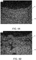
- FIGS. 2A-4B are images of a device as shown in FIG. 1 .
- the hard shield material 202 can be any suitable substrate material.
- the hard shield material 20 can a metal.
- the term “metal” refers to an element of Groups 2 through 13, inclusive, plus selected elements in Groups 14 and 15 of the periodic table. Thus, the term “metal” broadly refers to the following elements:
- La lanthanum
- Ce cerium
- Pr praseodymium
- Nd neodymium
- promethium Pm
- Sm samarium
- Eu europium
- Gd gadolinium
- Tb terbium
- Dy dysprosium
- Ho holmium
- Er erbium
- Tm thulium
- Yb ytterbium
- Lu lutetium
- Group 14 or IVA germanium (Ge), tin (Sn), and lead (Pb).
- Group 15 or VA antimony (Sn) and bismuth (Bi).
- the hard shield material 20 can be steel, such as stainless steel, or aluminum.
- the hard shield material 20 can have a thickness ranging from about 1 mm to about 5 mm, such as from about 2 mm to about 4 mm, and as a further example about 3 mm thick. It is contemplated that any thickness within the disclosed ranges can be used as well.
- a layer 30 including aluminum or copper can be applied on top of the hard shield material 20.
- the layer 30 can be a roughened metal, such as a roughened layer of aluminum or a roughened layer of copper.
- this layer 30 can be applied using a twin wire arc spray process.
- the twin wire arc spray process can include various steps, such as: (A) providing a reaction chamber with at least one starting material selected from the group consisting of a metal, a metal alloy, a metal compound, and a ceramic; (B) operating a twin-wire arc nozzle, comprising two wires and a working gas being controllably fed into the chamber, to form an arc between two converging leading tips of the two wires to heat and melt the starting material at the leading tips for providing a stream of liquid droplets traveling in a predetermined direction; and (C) operating a high energy source for producing a vaporizing zone adjacent to the arc and inside the chamber wherein the liquid droplets are vaporized to form vapor species.
- the two wires can be continuously fed into the chamber with the leading tips of the wires continuously melted (and partially vaporized) at a high feeding rate for producing vapor material continuously without interruption and at a high throughput rate.
- the vapor material can impinge upon and deposit onto the hard shield material, such as the substrate, to form a thin film or coating.
- the temperature in the vicinity of the substrate surface can be regulated so that the vapor material condenses and forms a coating, such as a coating of aluminum or copper.
- the working gas can be selected from, for instance, hydrogen, oxygen, carbon, nitrogen, chlorine, fluorine, boron, and sulfur to form respectively metal hydrides, oxides, carbides, nitrides, chlorides, fluorides, borides, and sulfides and combinations thereof.
- the starting material could include two different materials in a wire.
- the two different materials could make up the two wires in such a fashion that the two wires have different material compositions.
- the two metal wires can be driven by powered rollers to come in physical contact with two respective conductive jackets which are supplied with "+” and "-" voltage or pulsed power through electrically conductive blocks.
- the voltage polarity may be reversed; i.e., "-" and “+” instead of "+” and “-”.
- the voltages can come from a DC or pulsed power source.
- the lower ends of the two wires can approach each other at an angle of approximately 30-60°. The two ends can be brought into contact with each other for a brief period of time. Such a "short circuit" contact can create an ultra-high temperature due to a high current density, leading to the formation of an ionized arc.
- a stable arc can be maintained provided that the current is constantly supplied, a certain level of gas pressure is maintained, and the wires are fed at a constant or pulsating speed.
- a stream of compressed air introduced through a gas passage from a gas source (e.g., a compressed air bottle), can also serve to carry the stream of liquid downward into the vaporization zone.
- the layer 30 including aluminum or copper can be applied on top of the hard shield material 20 at a thickness of about 0.001 mm to about 5 mm, for example from about 0.05 mm to about 4 mm, and as a further example from about 0.1 mm to about 3 mm.
- the layer 20 can be applied using a twin wire arc spray process to achieve a thickness of about 0.1 mm.
- a silicon layer 40 having a first thickness can be applied onto the layer 30 including aluminum or copper.
- the silicon layer 40 can be applied using a plasma spray process.
- the plasma spray process can use a DC electric arc to generate a stream of high temperature (1500° C) ionize plasma gas.
- a material, such as silicon can be carried in an inert gas stream into the plasma jet where it is heated and propelled towards a substrate, such as the exposed layer of aluminum or copper that was applied on top of the hard shield material.
- the plasma spray gun can include a copper anode and tungsten cathode, both of which can be water cooled.
- Plasma gas such as argon, nitrogen, hydrogen, and helium, can flow around the cathode and through the anode which can be shaped as a constricting nozzle.
- the silicon layer 40 having a first thickness can be present at a first thickness of about 0.05 mm to about 2 mm, for example from about 0.08 mm to about 1.5 mm, and as a further example from about 0.1 mm to about 1 mm.
- the layer 30 including aluminum or copper can produce stress and defects in the adjacent silicon layer 40 having a first thickness applied by a plasma spray process.
- these defects can be reduced or minimized due to the first thickness of the silicon layer 40.
- the defects may only be present within 20 nm into the silicon layer 40 from the layer including the aluminum or copper. The defects therefore would not extend all the way through the silicon layer 40.
- the silicon layer 40 having a first thickness can have similar properties to a silicon layer 50 having a second thickness and applied via a sputter deposition process.
- the device 10 can further include a silicon layer 50 having a second thickness that has been applied by a sputter deposition process onto the silicon layer 40 having a first thickness, which was applied by a plasma spray process.
- the silicon layer 50 can be present at a second thickness of from about 10 nm to about 100 nm, for example from about 30 nm to about 80 nm, and as a further example from about 45 nm to about 60 nm.
- a method of making the device 10 can include providing a hard shield material 20; applying on top of the hard shield material 20 a layer 30 using a twin wire arc spray process; and applying on top of the layer 30 applied using the twin wire arc spray process a silicon layer 40 having a first thickness using a plasma spray process.
- the hard shield material 20 can be any substrate material.
- the hard shield material 20 is steel or aluminum.
- the hard shield material 20 can be about 3 mm thick.
- the layer 30 applied using the twin wire arc spray process is a layer of aluminum. In another aspect, the layer 30 applied using the twin wire arc spray process is a layer of copper. The layer 30 applied using the twin wire arc spray can have a thickness around 1 mm.
- the silicon layer 40 having a first thickness applied using a plasma spray process can enable a thicker layer of silicon to be deposited.
- This silicon layer 40 can be applied in a layer thick enough to avoid and/or minimize the risk of defects occurring due to the presence of dissimilar materials. Additionally, because this thicker layer of silicon 40 is applied in a different process step it enables the sputter deposition of a silicon layer 50 having a second thickness to use less material, i.e., it is a thinner layer. The use of less material will reduce the likelihood that silicon would appear on the sputter coating chamber walls, falling off the walls, and creating dust on the device 10.
- the method of making the device 10 further comprises, after applying a silicon layer 40 having a first thickness using a plasma spray process, applying a silicon layer 50 having a second thickness in a sputtering process.
- the silicon layer 50 applied in a sputtering process can be present in a thickness of about 50 nm.
- the use of the two separate processes to apply the different thickness silicon layers 40, 50 can reduce defects in the resultant device 10, increase yield, increase throughput, and increase capacity. Additionally, the applied silicon layer can change a stress profile of the device. Further, the applied silicon layer can increase durability of the device.
- Example 1 - A device 10 was made as follows: A hard shield material 20 of stainless steel having a thickness of 3 mm was used as a substrate. A layer 30 of aluminum was applied onto the stainless steel sheet 20 using a twin wire arc spray process. The layer 30 of aluminum was 0.1 mm thick. A layer of silicon 40 having a first thickness was applied onto the layer 30 of aluminum using a plasma spray process. The layer of silicon 40 was 0.1 mm thick. A layer of silicon 50 having a second thickness was sputter deposited onto the plasma sprayed silicon layer 40 having a first thickness. The sputter deposited silicon layer 50 was 50 nm thick. FIGS. 2A-4B are images of the device made according to the method.
Landscapes
- Chemical & Material Sciences (AREA)
- Engineering & Computer Science (AREA)
- Organic Chemistry (AREA)
- Chemical Kinetics & Catalysis (AREA)
- Materials Engineering (AREA)
- Mechanical Engineering (AREA)
- Metallurgy (AREA)
- Physics & Mathematics (AREA)
- Plasma & Fusion (AREA)
- Inorganic Chemistry (AREA)
- General Chemical & Material Sciences (AREA)
- Analytical Chemistry (AREA)
- Coating By Spraying Or Casting (AREA)
- Physical Vapour Deposition (AREA)
- Health & Medical Sciences (AREA)
- Electromagnetism (AREA)
- Toxicology (AREA)
Abstract
Description
- The present disclosure generally relates to a device including a hard shield material; a layer including aluminum or copper; and a silicon layer having a first thickness. The device can also include a silicon layer having a second thickness. A method of making the device is also disclosed. The device can include less defects and can have increased durability.
- Excess coating material can attach to the walls of the sputter coating chamber. The coating on the walls of the sputter chamber can fracture, fall apart, and can create dust. Each cycle of use of the sputter coating chamber increases the number and types of defects that can be seen in the coatings deposited in the coating chamber. The increased number of defects results in a decreased yield, which leads to a lower throughput through the coating chamber, which leads to lower capacity.
- In an aspect, there is disclosed a device including a hard shield material; a layer including aluminum or copper; and a silicon layer.
- The device may further comprise a silicon layer having a second thickness.
- The hard shield material may be a metal.
- The hard shield material may be an element of Groups 1 through 13 of the periodic table.
- The hard shield material may be steel or aluminum.
- The hard shield material may have a thickness ranging from about 1 mm to about 5 mm.
- The layer including aluminum or copper may be roughened.
- The layer including aluminium or copper may have a thickness of about 0.001 mm to about 5 mm.
- The silicon layer may be present at a first thickness of about 0.05 mm to about 2 mm.
- The silicon layer may be present at a second thickness from about 10 nm to about 100 nm.
- In another aspect, there is disclosed a method of making a device comprising providing a hard shield material; applying on top of the hard shield material a layer using a twin wire arc spray process; and applying on top of the layer applied using the twin wire arc spray process a silicon layer having a first thickness using a plasma spray process.
- The hard shield material may be steel or aluminum.
- The layer applied using the twin wire arc spray process may be a layer of aluminium.
- The layer applied using the twin wire arc spray process may be a layer of copper.
- The method may further comprise after applying a silicon layer using a plasma spray process, applying a silicon layer having a second thickness in a sputtering process.
- The applied silicon layer having a first thickness may change a stress profile of the device.
- The applied silicon layer having a first thickness may increase durability of the device.
- The twin arc spray process may include providing a reaction chamber with at least one starting material selected from the group consisting of a metal, a metal alloy, a metal compound, and a ceramic.
- The twin arc spray process may further include operating a twin-wire arc nozzle comprising two wires and a working gas being controllably fed into the reaction chamber to form an arc between two converging leading tips of the two wires to heat and melt the at least one starting material at the leading tips for providing a stream of liquid droplets traveling in a predetermined direction.
- The twin arc spray process may further include operating a high energy source for producing a vaporizing zone adjacent to the arc and inside the reaction chamber wherein the liquid droplets are vaporized to form vapor species.
- Additional features and advantages of various embodiments will be set forth, in part, in the description that follows, and will, in part, be apparent from the description, or may be learned by the practice of various embodiments. The objectives and other advantages of various embodiments will be realized and attained by means of the elements and combinations particularly pointed out in the description herein.
- The present disclosure in its several aspects and embodiments can be more fully understood from the detailed description and the accompanying drawings, wherein:
-
FIG. 1 is a cross-section of a device according to an aspect of the invention; -
FIGS. 2A and 2B are images of a device according to an aspect of the invention; -
FIGS. 3A and 3B are images of a device according to an aspect of the invention; and -
FIGS. 4A and 4B are images of a device according to an aspect of the invention; - Throughout this specification and figures like reference numbers identify like elements.
- It is to be understood that both the foregoing general description and the following detailed description are exemplary and explanatory only, and are intended to provide an explanation of various embodiments of the present teachings. The layers/components shown in each Figure may be described with regard to a particular Figure, but it is understood that the description of a particular layer/component would be applicable to the equivalent layer/component in the other Figures.
- In its broad and varied embodiments, disclosed herein is a
device 10 including ahard shield material 20; alayer 30 including aluminum or copper; and asilicon layer 40 having a first thickness. As shown inFIG. 1 , the device can include ahard shield material 20; alayer 30 including aluminum or copper; asilicon layer 40 having a first thickness; and asilicon layer 50 having a second thickness.FIGS. 2A-4B are images of a device as shown inFIG. 1 . - The hard shield material 202 can be any suitable substrate material. In an aspect, the
hard shield material 20 can a metal. As used herein, the term "metal" refers to an element of Groups 2 through 13, inclusive, plus selected elements in Groups 14 and 15 of the periodic table. Thus, the term "metal" broadly refers to the following elements: - Group 2 or IIA: beryllium (Be), magnesium (Mg), calcium (Ca), strontium (Sr), barium (Ba), and radium (Ra).
- Groups 3-12: transition metals (Groups IIIB, IVB, VB, VIB, VIIB, VIII, IB, and IIB), including scandium (Sc), yttrium (Y), titanium (Ti), zirconium (Zr), hafnium (Hf), vanadium (V), niobium (Nb), tantalum (Ta), chromium (Cr), molybdenum (Mo), tungsten (W), manganese (Mn), technetium (Tc), rhenium (Re), iron (Fe), ruthenium (Ru), osmium (Os) cobalt (Co), rhodium (Rh), iridium (Ir), nickel (Ni), palladium (Pd), platinum (Pt), copper (Cu), silver (Ag), gold (Au), zinc (Zn), cadmium (Cd), and mercury (Hg).
- Group 13 or IIIA: boron (B), aluminum (Al), gallium (Ga), indium (In), and thallium (TI).
- Lanthanides: lanthanum (La), cerium (Ce), praseodymium (Pr), neodymium (Nd), promethium (Pm), samarium (Sm), europium (Eu), gadolinium (Gd), terbium (Tb), dysprosium (Dy), holmium (Ho), erbium (Er), thulium (Tm), ytterbium (Yb), and lutetium (Lu).
- Group 14 or IVA: germanium (Ge), tin (Sn), and lead (Pb).
- Group 15 or VA: antimony (Sn) and bismuth (Bi).
- In an aspect, the
hard shield material 20 can be steel, such as stainless steel, or aluminum. Thehard shield material 20 can have a thickness ranging from about 1 mm to about 5 mm, such as from about 2 mm to about 4 mm, and as a further example about 3 mm thick. It is contemplated that any thickness within the disclosed ranges can be used as well. - In the disclosed
device 10, alayer 30 including aluminum or copper can be applied on top of thehard shield material 20. Thelayer 30 can be a roughened metal, such as a roughened layer of aluminum or a roughened layer of copper. In an aspect, thislayer 30 can be applied using a twin wire arc spray process. The twin wire arc spray process can include various steps, such as: (A) providing a reaction chamber with at least one starting material selected from the group consisting of a metal, a metal alloy, a metal compound, and a ceramic; (B) operating a twin-wire arc nozzle, comprising two wires and a working gas being controllably fed into the chamber, to form an arc between two converging leading tips of the two wires to heat and melt the starting material at the leading tips for providing a stream of liquid droplets traveling in a predetermined direction; and (C) operating a high energy source for producing a vaporizing zone adjacent to the arc and inside the chamber wherein the liquid droplets are vaporized to form vapor species. The two wires can be continuously fed into the chamber with the leading tips of the wires continuously melted (and partially vaporized) at a high feeding rate for producing vapor material continuously without interruption and at a high throughput rate. The vapor material can impinge upon and deposit onto the hard shield material, such as the substrate, to form a thin film or coating. The temperature in the vicinity of the substrate surface can be regulated so that the vapor material condenses and forms a coating, such as a coating of aluminum or copper. - The working gas can be selected from, for instance, hydrogen, oxygen, carbon, nitrogen, chlorine, fluorine, boron, and sulfur to form respectively metal hydrides, oxides, carbides, nitrides, chlorides, fluorides, borides, and sulfides and combinations thereof.
- The starting material could include two different materials in a wire. The two different materials could make up the two wires in such a fashion that the two wires have different material compositions.
- The two metal wires can be driven by powered rollers to come in physical contact with two respective conductive jackets which are supplied with "+" and "-" voltage or pulsed power through electrically conductive blocks. The voltage polarity may be reversed; i.e., "-" and "+" instead of "+" and "-". The voltages can come from a DC or pulsed power source. The lower ends of the two wires can approach each other at an angle of approximately 30-60°. The two ends can be brought into contact with each other for a brief period of time. Such a "short circuit" contact can create an ultra-high temperature due to a high current density, leading to the formation of an ionized arc. A stable arc can be maintained provided that the current is constantly supplied, a certain level of gas pressure is maintained, and the wires are fed at a constant or pulsating speed. A stream of compressed air, introduced through a gas passage from a gas source (e.g., a compressed air bottle), can also serve to carry the stream of liquid downward into the vaporization zone.
- The
layer 30 including aluminum or copper can be applied on top of thehard shield material 20 at a thickness of about 0.001 mm to about 5 mm, for example from about 0.05 mm to about 4 mm, and as a further example from about 0.1 mm to about 3 mm. In an aspect, thelayer 20 can be applied using a twin wire arc spray process to achieve a thickness of about 0.1 mm. - In the disclosed
device 10, asilicon layer 40 having a first thickness can be applied onto thelayer 30 including aluminum or copper. Thesilicon layer 40 can be applied using a plasma spray process. The plasma spray process can use a DC electric arc to generate a stream of high temperature (1500° C) ionize plasma gas. A material, such as silicon, can be carried in an inert gas stream into the plasma jet where it is heated and propelled towards a substrate, such as the exposed layer of aluminum or copper that was applied on top of the hard shield material. The plasma spray gun can include a copper anode and tungsten cathode, both of which can be water cooled. Plasma gas, such as argon, nitrogen, hydrogen, and helium, can flow around the cathode and through the anode which can be shaped as a constricting nozzle. - The
silicon layer 40 having a first thickness can be present at a first thickness of about 0.05 mm to about 2 mm, for example from about 0.08 mm to about 1.5 mm, and as a further example from about 0.1 mm to about 1 mm. - Stress and the defects resulting therefrom can occur due to the presence of dissimilar materials in relation to one another. For example, the
layer 30 including aluminum or copper can produce stress and defects in theadjacent silicon layer 40 having a first thickness applied by a plasma spray process. However, these defects can be reduced or minimized due to the first thickness of thesilicon layer 40. For example, the defects may only be present within 20 nm into thesilicon layer 40 from the layer including the aluminum or copper. The defects therefore would not extend all the way through thesilicon layer 40. - Additionally, the
silicon layer 40 having a first thickness can have similar properties to asilicon layer 50 having a second thickness and applied via a sputter deposition process. - The
device 10 can further include asilicon layer 50 having a second thickness that has been applied by a sputter deposition process onto thesilicon layer 40 having a first thickness, which was applied by a plasma spray process. Thesilicon layer 50 can be present at a second thickness of from about 10 nm to about 100 nm, for example from about 30 nm to about 80 nm, and as a further example from about 45 nm to about 60 nm. - A method of making the
device 10 can include providing ahard shield material 20; applying on top of the hard shield material 20 alayer 30 using a twin wire arc spray process; and applying on top of thelayer 30 applied using the twin wire arc spray process asilicon layer 40 having a first thickness using a plasma spray process. - As discussed above, the
hard shield material 20 can be any substrate material. In an aspect, thehard shield material 20 is steel or aluminum. Thehard shield material 20 can be about 3 mm thick. - In an aspect, the
layer 30 applied using the twin wire arc spray process is a layer of aluminum. In another aspect, thelayer 30 applied using the twin wire arc spray process is a layer of copper. Thelayer 30 applied using the twin wire arc spray can have a thickness around 1 mm. - The
silicon layer 40 having a first thickness applied using a plasma spray process can enable a thicker layer of silicon to be deposited. Thissilicon layer 40 can be applied in a layer thick enough to avoid and/or minimize the risk of defects occurring due to the presence of dissimilar materials. Additionally, because this thicker layer ofsilicon 40 is applied in a different process step it enables the sputter deposition of asilicon layer 50 having a second thickness to use less material, i.e., it is a thinner layer. The use of less material will reduce the likelihood that silicon would appear on the sputter coating chamber walls, falling off the walls, and creating dust on thedevice 10. - The method of making the
device 10 further comprises, after applying asilicon layer 40 having a first thickness using a plasma spray process, applying asilicon layer 50 having a second thickness in a sputtering process. Thesilicon layer 50 applied in a sputtering process can be present in a thickness of about 50 nm. - The use of the two separate processes to apply the different thickness silicon layers 40, 50 can reduce defects in the
resultant device 10, increase yield, increase throughput, and increase capacity. Additionally, the applied silicon layer can change a stress profile of the device. Further, the applied silicon layer can increase durability of the device. - Example 1 -
A device 10 was made as follows: Ahard shield material 20 of stainless steel having a thickness of 3 mm was used as a substrate. Alayer 30 of aluminum was applied onto thestainless steel sheet 20 using a twin wire arc spray process. Thelayer 30 of aluminum was 0.1 mm thick. A layer ofsilicon 40 having a first thickness was applied onto thelayer 30 of aluminum using a plasma spray process. The layer ofsilicon 40 was 0.1 mm thick. A layer ofsilicon 50 having a second thickness was sputter deposited onto the plasma sprayedsilicon layer 40 having a first thickness. The sputter depositedsilicon layer 50 was 50 nm thick.FIGS. 2A-4B are images of the device made according to the method. - From the foregoing description, those skilled in the art can appreciate that the present teachings can be implemented in a variety of forms. Therefore, while these teachings have been described in connection with particular embodiments and examples thereof, the true scope of the present teachings should not be so limited. Various changes and modifications may be made without departing from the scope of the teachings herein.
- This scope disclosure is to be broadly construed. It is intended that this disclosure disclose equivalents, means, systems and methods to achieve the devices, activities and mechanical actions disclosed herein. For each device, article, method, mean, mechanical element or mechanism disclosed, it is intended that this disclosure also encompass in its disclosure and teaches equivalents, means, systems and methods for practicing the many aspects, mechanisms and devices disclosed herein. Additionally, this disclosure regards a coating and its many aspects, features and elements. Such a device can be dynamic in its use and operation, this disclosure is intended to encompass the equivalents, means, systems and methods of the use of the device and/or article of manufacture and its many aspects consistent with the description and spirit of the operations and functions disclosed herein. The claims of this application are likewise to be broadly construed.
- The description of the inventions herein in their many embodiments is merely exemplary in nature and, thus, variations that do not depart from the gist of the invention are intended to be within the scope of the invention. Such variations are not to be regarded as a departure from the spirit and scope of the invention.
Claims (15)
- A device comprising:a hard shield material;a layer including aluminum or copper; anda silicon layer having a first thickness.
- The device of claim 1, further comprising a silicon layer having a second thickness.
- The device of claim 1, wherein the hard shield material is a metal.
- The device of claim 1, wherein the hard shield material is steel or aluminum.
- The device of claim 1, wherein the hard shield material has a thickness ranging from about 1 mm to about 5 mm; and the layer including aluminum or copper can have a thickness of about 0.001 mm to about 5 mm.
- The device of claim 1, wherein the layer including aluminum or copper is roughened.
- The device of claim 2, wherein the silicon layer is present at a first thickness of about 0.05 mm to about 2 mm; and wherein the silicon layer is present at a second thickness from about 10 nm to about 100 nm.
- A method of making a device, comprising:providing a hard shield material;applying on top of the hard shield material a layer using a twin wire arc spray process; andapplying on top of the layer applied using the twin wire arc spray process a silicon layer having a first thickness using a plasma spray process.
- The method of claim 8, wherein the layer applied using the twin wire arc spray process is a layer of aluminum.
- The method of claim 8, wherein the layer applied using the twin wire arc spray process is a layer of copper.
- The method of claim 8, further comprising after applying a silicon layer using a plasma spray process, applying a silicon layer having a second thickness in a sputtering process.
- The method of claim 8, wherein the applied silicon layer having a first thickness changes a stress profile of the device and/or increases durability of the device.
- The method of claim 8, wherein the twin arc spray process includes providing a reaction chamber with at least one starting material selected from the group consisting of a metal, a metal alloy, a metal compound, and a ceramic.
- The method of claim 13, wherein the twin arc spray process further includes operating a twin-wire arc nozzle comprising two wires and a working gas being controllably fed into the reaction chamber to form an arc between two converging leading tips of the two wires to heat and melt the at least one starting material at the leading tips for providing a stream of liquid droplets traveling in a predetermined direction.
- The method of claim 14, wherein the twin arc spray process further includes operating a high energy source for producing a vaporizing zone adjacent to the arc and inside the reaction chamber wherein the liquid droplets are vaporized to form vapor species.
Applications Claiming Priority (1)
| Application Number | Priority Date | Filing Date | Title |
|---|---|---|---|
| US201862619052P | 2018-01-18 | 2018-01-18 |
Publications (1)
| Publication Number | Publication Date |
|---|---|
| EP3514255A1 true EP3514255A1 (en) | 2019-07-24 |
Family
ID=65041663
Family Applications (1)
| Application Number | Title | Priority Date | Filing Date |
|---|---|---|---|
| EP19152560.9A Pending EP3514255A1 (en) | 2018-01-18 | 2019-01-18 | Silicon coating on hard shields |
Country Status (6)
| Country | Link |
|---|---|
| US (1) | US11486042B2 (en) |
| EP (1) | EP3514255A1 (en) |
| JP (1) | JP7199978B2 (en) |
| KR (1) | KR102259204B1 (en) |
| CN (1) | CN110060980B (en) |
| TW (1) | TWI729346B (en) |
Citations (4)
| Publication number | Priority date | Publication date | Assignee | Title |
|---|---|---|---|---|
| US5082760A (en) * | 1987-11-10 | 1992-01-21 | Fuji Xerox Co., Ltd. | Method for preparing an electrophotographic photoreceptor having a charge transporting layer containing aluminum oxide |
| US6123999A (en) * | 1997-03-21 | 2000-09-26 | E. I. Du Pont De Nemours And Company | Wear resistant non-stick resin coated substrates |
| US20120321812A1 (en) * | 2011-06-14 | 2012-12-20 | Yitzhak Vanek | Process for forming porous metal coating on surfaces |
| US20170145553A1 (en) * | 2015-11-24 | 2017-05-25 | Applied Materials, Inc. | Pre-coated shield using in vhf-rf pvd chambers |
Family Cites Families (11)
| Publication number | Priority date | Publication date | Assignee | Title |
|---|---|---|---|---|
| US4427516A (en) | 1981-08-24 | 1984-01-24 | Bell Telephone Laboratories, Incorporated | Apparatus and method for plasma-assisted etching of wafers |
| JPH0782240B2 (en) * | 1986-09-04 | 1995-09-06 | 富士ゼロックス株式会社 | Electrophotographic photoreceptor |
| JP2595575B2 (en) | 1987-11-10 | 1997-04-02 | 富士ゼロックス株式会社 | Manufacturing method of electrophotographic photoreceptor |
| JP2720448B2 (en) | 1988-03-04 | 1998-03-04 | 富士ゼロックス株式会社 | Manufacturing method of electrophotographic photoreceptor |
| JP2002292346A (en) * | 2001-03-29 | 2002-10-08 | Sharp Corp | Adhesive film recovery device and method for recovering adhesive film |
| US7026009B2 (en) | 2002-03-27 | 2006-04-11 | Applied Materials, Inc. | Evaluation of chamber components having textured coatings |
| US8500963B2 (en) * | 2006-10-26 | 2013-08-06 | Applied Materials, Inc. | Sputtering of thermally resistive materials including metal chalcogenides |
| SG162642A1 (en) * | 2009-01-06 | 2010-07-29 | Frontken Singapore Pte Ltd | Techniques for maintaining a substrate processing system |
| US8734907B2 (en) * | 2012-02-02 | 2014-05-27 | Sematech, Inc. | Coating of shield surfaces in deposition systems |
| EP3460093A3 (en) * | 2015-02-13 | 2019-06-19 | Entegris, Inc. | Coatings for enhancement of properties and performance of substrate articles and apparatus |
| JP6332215B2 (en) * | 2015-09-25 | 2018-05-30 | 富士ゼロックス株式会社 | Image forming apparatus unit, process cartridge, image forming apparatus, and electrophotographic photosensitive member |
-
2019
- 2019-01-17 US US16/250,842 patent/US11486042B2/en active Active
- 2019-01-18 JP JP2019007233A patent/JP7199978B2/en active Active
- 2019-01-18 CN CN201910108416.8A patent/CN110060980B/en active Active
- 2019-01-18 EP EP19152560.9A patent/EP3514255A1/en active Pending
- 2019-01-18 KR KR1020190006873A patent/KR102259204B1/en active Active
- 2019-01-18 TW TW108102020A patent/TWI729346B/en active
Patent Citations (4)
| Publication number | Priority date | Publication date | Assignee | Title |
|---|---|---|---|---|
| US5082760A (en) * | 1987-11-10 | 1992-01-21 | Fuji Xerox Co., Ltd. | Method for preparing an electrophotographic photoreceptor having a charge transporting layer containing aluminum oxide |
| US6123999A (en) * | 1997-03-21 | 2000-09-26 | E. I. Du Pont De Nemours And Company | Wear resistant non-stick resin coated substrates |
| US20120321812A1 (en) * | 2011-06-14 | 2012-12-20 | Yitzhak Vanek | Process for forming porous metal coating on surfaces |
| US20170145553A1 (en) * | 2015-11-24 | 2017-05-25 | Applied Materials, Inc. | Pre-coated shield using in vhf-rf pvd chambers |
Non-Patent Citations (1)
| Title |
|---|
| VIJAY A. SETHURAMAN ET AL: "Increased cycling efficiency and rate capability of copper-coated silicon anodes in lithium-ion batteries", JOURNAL OF POWER SOURCES, vol. 196, no. 1, 23 June 2010 (2010-06-23), pages 393 - 398, XP055215683, ISSN: 0378-7753, DOI: 10.1016/j.jpowsour.2010.06.043 * |
Also Published As
| Publication number | Publication date |
|---|---|
| JP2019123939A (en) | 2019-07-25 |
| US11486042B2 (en) | 2022-11-01 |
| CN110060980A (en) | 2019-07-26 |
| JP7199978B2 (en) | 2023-01-06 |
| TWI729346B (en) | 2021-06-01 |
| CN110060980B (en) | 2024-02-20 |
| KR20190088430A (en) | 2019-07-26 |
| TW201932646A (en) | 2019-08-16 |
| US20190218669A1 (en) | 2019-07-18 |
| KR102259204B1 (en) | 2021-05-31 |
Similar Documents
| Publication | Publication Date | Title |
|---|---|---|
| CN107109626B (en) | Device for forming a coating on a surface of a component | |
| KR101728923B1 (en) | Production method with thermal projection of a target | |
| US3791852A (en) | High rate deposition of carbides by activated reactive evaporation | |
| US20040065170A1 (en) | Method for producing nano-structured materials | |
| WO2009072318A1 (en) | Method of forming black yttrium oxide sprayed coating and member provided with black yttrium oxide sprayed coating | |
| US11486042B2 (en) | Silicon coating on hard shields | |
| HK40010973A (en) | Silicon coating on hard shields | |
| HK40010973B (en) | Silicon coating on hard shields | |
| US5262033A (en) | Apparatus for the continuous etchings and aluminum plating of stainless steel strips | |
| US20030234176A1 (en) | Production of carbon and carbon-based materials | |
| WO2013114942A1 (en) | Method for blackening white fluoride spray coating, and fluoride spray coating covering member having black layer on surface | |
| KR102890171B1 (en) | Sputtering target and manufacturing method thereof | |
| US20050199861A1 (en) | Manufacturing method for transparent and conductive coatings | |
| US20030102288A1 (en) | System and method for production of optically transparent and electrically conductive | |
| TWI821944B (en) | Sputtering target, method of manufacturing the same, and method of manufacturing alloy thin film | |
| CN111996486A (en) | Component for film forming apparatus and film forming apparatus provided with component for film forming apparatus | |
| JP4209277B2 (en) | Method for producing plasma corrosion resistant thermal spray member | |
| JPH1068069A (en) | Method of forming metal boride film | |
| AU756273B2 (en) | Method and apparatus for producing material vapour | |
| Demchyshyn et al. | Linear Vacuum ARC Evaporators for Deposition of Functional Multi-Purpose Coatings | |
| JP5406317B2 (en) | Blackening method of white fluoride spray coating and fluoride spray coating covering member having black layer on surface | |
| JP5406323B2 (en) | Blackening method of white fluoride spray coating and fluoride spray coating covering member having black layer on surface | |
| PL239275B1 (en) | Method of applying to the substrate ultrathin functional coatings with increased physical and chemical resistance by magnetronic method and substrates with functional coatings obtained by this method | |
| AU2001272216A1 (en) | Production of carbon and carbon-based materials | |
| Ramalingam | Minneapolis, Minnesota 55455 |
Legal Events
| Date | Code | Title | Description |
|---|---|---|---|
| PUAI | Public reference made under article 153(3) epc to a published international application that has entered the european phase |
Free format text: ORIGINAL CODE: 0009012 |
|
| STAA | Information on the status of an ep patent application or granted ep patent |
Free format text: STATUS: THE APPLICATION HAS BEEN PUBLISHED |
|
| AK | Designated contracting states |
Kind code of ref document: A1 Designated state(s): AL AT BE BG CH CY CZ DE DK EE ES FI FR GB GR HR HU IE IS IT LI LT LU LV MC MK MT NL NO PL PT RO RS SE SI SK SM TR |
|
| AX | Request for extension of the european patent |
Extension state: BA ME |
|
| STAA | Information on the status of an ep patent application or granted ep patent |
Free format text: STATUS: REQUEST FOR EXAMINATION WAS MADE |
|
| 17P | Request for examination filed |
Effective date: 20200124 |
|
| RBV | Designated contracting states (corrected) |
Designated state(s): AL AT BE BG CH CY CZ DE DK EE ES FI FR GB GR HR HU IE IS IT LI LT LU LV MC MK MT NL NO PL PT RO RS SE SI SK SM TR |
|
| STAA | Information on the status of an ep patent application or granted ep patent |
Free format text: STATUS: EXAMINATION IS IN PROGRESS |
|
| 17Q | First examination report despatched |
Effective date: 20210924 |
|
| RAP3 | Party data changed (applicant data changed or rights of an application transferred) |
Owner name: VIAVI SOLUTIONS INC. |
|
| P01 | Opt-out of the competence of the unified patent court (upc) registered |
Effective date: 20230530 |
|
| GRAP | Despatch of communication of intention to grant a patent |
Free format text: ORIGINAL CODE: EPIDOSNIGR1 |
|
| STAA | Information on the status of an ep patent application or granted ep patent |
Free format text: STATUS: GRANT OF PATENT IS INTENDED |
|
| INTG | Intention to grant announced |
Effective date: 20260504 |