EP3513475B1 - Anlage zum übertragen elektrischer leistung mit filtereinheit - Google Patents
Anlage zum übertragen elektrischer leistung mit filtereinheit Download PDFInfo
- Publication number
- EP3513475B1 EP3513475B1 EP16797479.9A EP16797479A EP3513475B1 EP 3513475 B1 EP3513475 B1 EP 3513475B1 EP 16797479 A EP16797479 A EP 16797479A EP 3513475 B1 EP3513475 B1 EP 3513475B1
- Authority
- EP
- European Patent Office
- Prior art keywords
- voltage
- filter unit
- converter
- filter
- installation
- Prior art date
- Legal status (The legal status is an assumption and is not a legal conclusion. Google has not performed a legal analysis and makes no representation as to the accuracy of the status listed.)
- Active
Links
- 238000009434 installation Methods 0.000 title claims description 9
- 230000007935 neutral effect Effects 0.000 claims description 18
- 238000004804 winding Methods 0.000 claims description 7
- 239000004065 semiconductor Substances 0.000 description 21
- 239000003990 capacitor Substances 0.000 description 15
- 238000001914 filtration Methods 0.000 description 3
- 238000004146 energy storage Methods 0.000 description 2
- 238000009499 grossing Methods 0.000 description 2
- 238000002955 isolation Methods 0.000 description 2
- 230000003213 activating effect Effects 0.000 description 1
- 230000005540 biological transmission Effects 0.000 description 1
- 238000013016 damping Methods 0.000 description 1
- 230000001419 dependent effect Effects 0.000 description 1
- 230000001105 regulatory effect Effects 0.000 description 1
Images

Classifications
-
- H—ELECTRICITY
- H02—GENERATION; CONVERSION OR DISTRIBUTION OF ELECTRIC POWER
- H02J—CIRCUIT ARRANGEMENTS OR SYSTEMS FOR SUPPLYING OR DISTRIBUTING ELECTRIC POWER; SYSTEMS FOR STORING ELECTRIC ENERGY
- H02J3/00—Circuit arrangements for ac mains or ac distribution networks
- H02J3/26—Arrangements for eliminating or reducing asymmetry in polyphase networks
-
- H—ELECTRICITY
- H02—GENERATION; CONVERSION OR DISTRIBUTION OF ELECTRIC POWER
- H02J—CIRCUIT ARRANGEMENTS OR SYSTEMS FOR SUPPLYING OR DISTRIBUTING ELECTRIC POWER; SYSTEMS FOR STORING ELECTRIC ENERGY
- H02J3/00—Circuit arrangements for ac mains or ac distribution networks
- H02J3/34—Arrangements for transfer of electric power between networks of substantially different frequency
-
- H—ELECTRICITY
- H02—GENERATION; CONVERSION OR DISTRIBUTION OF ELECTRIC POWER
- H02M—APPARATUS FOR CONVERSION BETWEEN AC AND AC, BETWEEN AC AND DC, OR BETWEEN DC AND DC, AND FOR USE WITH MAINS OR SIMILAR POWER SUPPLY SYSTEMS; CONVERSION OF DC OR AC INPUT POWER INTO SURGE OUTPUT POWER; CONTROL OR REGULATION THEREOF
- H02M1/00—Details of apparatus for conversion
- H02M1/14—Arrangements for reducing ripples from dc input or output
- H02M1/143—Arrangements for reducing ripples from dc input or output using compensating arrangements
-
- H—ELECTRICITY
- H02—GENERATION; CONVERSION OR DISTRIBUTION OF ELECTRIC POWER
- H02M—APPARATUS FOR CONVERSION BETWEEN AC AND AC, BETWEEN AC AND DC, OR BETWEEN DC AND DC, AND FOR USE WITH MAINS OR SIMILAR POWER SUPPLY SYSTEMS; CONVERSION OF DC OR AC INPUT POWER INTO SURGE OUTPUT POWER; CONTROL OR REGULATION THEREOF
- H02M5/00—Conversion of ac power input into ac power output, e.g. for change of voltage, for change of frequency, for change of number of phases
- H02M5/40—Conversion of ac power input into ac power output, e.g. for change of voltage, for change of frequency, for change of number of phases with intermediate conversion into dc
- H02M5/42—Conversion of ac power input into ac power output, e.g. for change of voltage, for change of frequency, for change of number of phases with intermediate conversion into dc by static converters
- H02M5/44—Conversion of ac power input into ac power output, e.g. for change of voltage, for change of frequency, for change of number of phases with intermediate conversion into dc by static converters using discharge tubes or semiconductor devices to convert the intermediate dc into ac
- H02M5/453—Conversion of ac power input into ac power output, e.g. for change of voltage, for change of frequency, for change of number of phases with intermediate conversion into dc by static converters using discharge tubes or semiconductor devices to convert the intermediate dc into ac using devices of a triode or transistor type requiring continuous application of a control signal
- H02M5/458—Conversion of ac power input into ac power output, e.g. for change of voltage, for change of frequency, for change of number of phases with intermediate conversion into dc by static converters using discharge tubes or semiconductor devices to convert the intermediate dc into ac using devices of a triode or transistor type requiring continuous application of a control signal using semiconductor devices only
-
- H—ELECTRICITY
- H02—GENERATION; CONVERSION OR DISTRIBUTION OF ELECTRIC POWER
- H02M—APPARATUS FOR CONVERSION BETWEEN AC AND AC, BETWEEN AC AND DC, OR BETWEEN DC AND DC, AND FOR USE WITH MAINS OR SIMILAR POWER SUPPLY SYSTEMS; CONVERSION OF DC OR AC INPUT POWER INTO SURGE OUTPUT POWER; CONTROL OR REGULATION THEREOF
- H02M7/00—Conversion of ac power input into dc power output; Conversion of dc power input into ac power output
- H02M7/42—Conversion of dc power input into ac power output without possibility of reversal
- H02M7/44—Conversion of dc power input into ac power output without possibility of reversal by static converters
- H02M7/48—Conversion of dc power input into ac power output without possibility of reversal by static converters using discharge tubes with control electrode or semiconductor devices with control electrode
- H02M7/483—Converters with outputs that each can have more than two voltages levels
- H02M7/4835—Converters with outputs that each can have more than two voltages levels comprising two or more cells, each including a switchable capacitor, the capacitors having a nominal charge voltage which corresponds to a given fraction of the input voltage, and the capacitors being selectively connected in series to determine the instantaneous output voltage
-
- H—ELECTRICITY
- H02—GENERATION; CONVERSION OR DISTRIBUTION OF ELECTRIC POWER
- H02J—CIRCUIT ARRANGEMENTS OR SYSTEMS FOR SUPPLYING OR DISTRIBUTING ELECTRIC POWER; SYSTEMS FOR STORING ELECTRIC ENERGY
- H02J3/00—Circuit arrangements for ac mains or ac distribution networks
- H02J3/36—Arrangements for transfer of electric power between ac networks via a high-tension dc link
- H02J2003/365—Reducing harmonics or oscillations in HVDC
-
- H—ELECTRICITY
- H02—GENERATION; CONVERSION OR DISTRIBUTION OF ELECTRIC POWER
- H02J—CIRCUIT ARRANGEMENTS OR SYSTEMS FOR SUPPLYING OR DISTRIBUTING ELECTRIC POWER; SYSTEMS FOR STORING ELECTRIC ENERGY
- H02J2300/00—Systems for supplying or distributing electric power characterised by decentralized, dispersed, or local generation
- H02J2300/20—The dispersed energy generation being of renewable origin
- H02J2300/28—The renewable source being wind energy
-
- H—ELECTRICITY
- H02—GENERATION; CONVERSION OR DISTRIBUTION OF ELECTRIC POWER
- H02J—CIRCUIT ARRANGEMENTS OR SYSTEMS FOR SUPPLYING OR DISTRIBUTING ELECTRIC POWER; SYSTEMS FOR STORING ELECTRIC ENERGY
- H02J3/00—Circuit arrangements for ac mains or ac distribution networks
- H02J3/38—Arrangements for parallely feeding a single network by two or more generators, converters or transformers
- H02J3/381—Dispersed generators
-
- Y—GENERAL TAGGING OF NEW TECHNOLOGICAL DEVELOPMENTS; GENERAL TAGGING OF CROSS-SECTIONAL TECHNOLOGIES SPANNING OVER SEVERAL SECTIONS OF THE IPC; TECHNICAL SUBJECTS COVERED BY FORMER USPC CROSS-REFERENCE ART COLLECTIONS [XRACs] AND DIGESTS
- Y02—TECHNOLOGIES OR APPLICATIONS FOR MITIGATION OR ADAPTATION AGAINST CLIMATE CHANGE
- Y02E—REDUCTION OF GREENHOUSE GAS [GHG] EMISSIONS, RELATED TO ENERGY GENERATION, TRANSMISSION OR DISTRIBUTION
- Y02E40/00—Technologies for an efficient electrical power generation, transmission or distribution
- Y02E40/50—Arrangements for eliminating or reducing asymmetry in polyphase networks
-
- Y—GENERAL TAGGING OF NEW TECHNOLOGICAL DEVELOPMENTS; GENERAL TAGGING OF CROSS-SECTIONAL TECHNOLOGIES SPANNING OVER SEVERAL SECTIONS OF THE IPC; TECHNICAL SUBJECTS COVERED BY FORMER USPC CROSS-REFERENCE ART COLLECTIONS [XRACs] AND DIGESTS
- Y02—TECHNOLOGIES OR APPLICATIONS FOR MITIGATION OR ADAPTATION AGAINST CLIMATE CHANGE
- Y02E—REDUCTION OF GREENHOUSE GAS [GHG] EMISSIONS, RELATED TO ENERGY GENERATION, TRANSMISSION OR DISTRIBUTION
- Y02E60/00—Enabling technologies; Technologies with a potential or indirect contribution to GHG emissions mitigation
- Y02E60/60—Arrangements for transfer of electric power between AC networks or generators via a high voltage DC link [HVCD]
Definitions
- the invention relates to a system for transmitting electrical power with a unidirectional rectifier that can be connected on the AC voltage side to a first AC voltage network, a self-commutated converter that can be connected on the AC voltage side to a second AC voltage network, and with a DC voltage connection that connects the rectifier and the converter on the DC side
- the invention also relates to a modular multi-stage converter.
- Such a system is for example from the US 8 120 202 B2 known.
- wind power systems of a wind park are connected to the first alternating voltage network.
- the electrical power generated by the wind turbines is transmitted to a supply network connected to the converter system by means of the known system.
- the unidirectional rectifier By means of the unidirectional rectifier, power transmission is only possible in one direction. This leads in particular to the fact that when designing the self-commutated converter, the fact that the first AC voltage network may not be symmetrical must be taken into account.
- An asymmetry in the first AC voltage network can arise, for example, due to a network fault or an asymmetrical operation of generators or motors.
- the asymmetry of the first AC voltage network can cause voltage fluctuations in the self-commutated converter, which must be taken into account when designing it.
- a correspondingly higher design of the self-commutated converter can disadvantageously increase the costs of the system.
- the EP 2 713 494 A1 discloses an arrangement with a DC filter on the DC circuit.
- the task of the The direct current filter is to isolate the direct current circuit from electromagnetic influences of a connected energy supply device in order to ensure electromagnetic compatibility.
- a modular multi-stage converter is for example from the document DE 10 103 031 A1 as known.
- a filter arrangement for filtering and damping harmonics or higher-frequency vibration packets and for shifting resonance points in electrical networks is from the document WO 91/09451 A1 known.
- the object of the invention is to propose a system mentioned at the beginning which is as inexpensive as possible.
- the object is achieved by a filter unit connected to the converter on the DC voltage side, which forms a current path to a neutral point of the second AC voltage network, the current path having a high impedance for a direct current and a low impedance for an AC current with the fundamental frequency of the second AC voltage network having.
- the current path of the filter unit can extend, for example, between a DC voltage pole of the converter or the DC voltage connection and the neutral point.
- the DC voltage side of the converter is connected to the neutral point by means of the filter unit.
- the filter unit can connect at least one DC voltage pole of the converter to the neutral point. Due to the high impedance for direct currents, there is no voltage loss on the DC voltage side of the converter.
- the high impedance for direct currents can be achieved, for example, by means of electrical isolation, expediently by means of capacitive electrical isolation.
- the low impedance of the filter unit for mains frequency alternating currents means that AC voltage components of a voltage on the DC voltage side of the converter are short-circuited to the neutral point, in particular those with the fundamental frequency of the AC voltage network. In this way you can get through an asymmetry of the first AC voltage network caused voltage fluctuations in the converter are advantageously reduced or even avoided. This advantageously lowers the costs of the entire system.
- the neutral point represents a connection to a fixed potential.
- the potential connection can be made with respect to one of the two AC voltage networks.
- the neutral point is a star point of a zigzag winding star point transformer connected to the second AC voltage network, which is also referred to below as a grounding transformer.
- the current path of the filter unit extends, for example, between one of the DC voltage poles of the converter or the DC voltage connection and the star point of the grounding transformer. This is particularly advantageous if the filter unit is arranged in close proximity to the converter, so that the connection to the second AC voltage network is not complex.
- the filter unit advantageously comprises exclusively passive filter components. Passive filter components are particularly cheap to install and operate, especially because they do not require any regulation.
- a passive filter component can be, for example, a choke, a capacitance in the form of a capacitor, a resistance element or a combination of these or similar components.
- the filter unit comprises a series connection of an inductance and a capacitance.
- the filter unit thus forms a suction circuit that the Can filter out alternating voltage components with a suitable design.
- the inductance is, for example, a filter choke, the capacitance correspondingly a filter capacitor.
- the capacitance and the inductance are designed in such a way that a resonance frequency of the filter unit is matched to the operating frequency or fundamental frequency of the second AC voltage network.
- a particularly low impedance for the alternating current with the fundamental frequency of the alternating voltage network and thus a particularly effective filtering is provided.
- f 1 / (2 * Pi * (L * C) ⁇ (1/2)), where f denotes the resonance frequency of the filter unit .
- the filter unit comprises a current branch which extends between a positive DC voltage pole of the converter and a negative DC voltage pole of the converter, the current branch having a first filter with a series connection of a first inductance and a first capacitance and a second filter with a series connection with a second inductance and a second capacitance, wherein a potential point between the first and the second filter is connected to the neutral point.
- the current branch can correspondingly also extend between a first and a second DC voltage pole of the DC voltage line.
- the filter unit thus comprises two sub-filters.
- the first sub-filter is arranged between the first DC voltage pole of the converter or the DC voltage connection and the neutral point.
- the second sub-filter is between the neutral point and the second DC voltage pole of the converter or the Direct voltage connection arranged. In this way, particularly effective filtering of the AC voltage components in the DC voltage is implemented.
- the unidirectional rectifier is preferably a diode rectifier.
- Diode rectifiers are particularly simple and robust in operation. At the same time, they are comparatively compact and lightweight compared to self-commutated converters, for example. In addition, the diode rectifier is relatively low-loss in operation.
- the diode rectifier can be implemented as a six-pulse, twelve-pulse or a 24-pulse bridge, for example.
- the self-commutated converter is a modular multi-stage converter (MMC).
- the modular multi-stage inverter is characterized by its modular design.
- the modular multi-stage converter comprises phase branches that each extend between an AC voltage connection of the multi-stage converter and one of the two DC voltage poles.
- the phase branches of the modular multi-stage converter each have a series connection of two-pole switching modules, each switching module comprising power semiconductor switches that can be switched on and off and an energy store, preferably in the form of a capacitor. Furthermore, each of the switching modules can be controlled individually.
- a voltage dropped across the phase branch is equal to the sum of voltages dropped across the associated switching modules.
- a particularly advantageous step-shaped converter voltage can be generated by means of the MMC.
- each switching module has a full bridge circuit with four power semiconductors that can be switched off and an energy store, which are connected to the energy store in such a way that one at the output terminals of the switch module is connected to the energy store falling energy storage voltage, a zero voltage or the inverse energy storage voltage can be generated.
- each switching module has a half-bridge circuit with two power semiconductors that can be switched off and an energy store, which are connected to the energy store in such a way that an energy store voltage dropping across the energy store or a zero voltage can be generated at the output terminals of the switch module.
- some of the switching modules of the MMC have full-bridge circuits and some other switching modules have half-bridge circuits.
- the use of an MMC in the system according to the invention is particularly advantageous.
- the provision of the filter unit enables the number of switching modules built into the MMC to be reduced in each phase branch. This allows an advantageous reduction in the costs of the MMC and of the entire system, because the switching modules are relatively expensive components.
- the electrical losses of the system are reduced, which further lowers the operating costs of the system.
- the invention also relates to a modular multi-stage converter which can be connected on the AC voltage side to an AC voltage network and on the DC voltage side to a DC voltage connection.
- the object of the invention is to provide such a modular multi-stage converter which is as inexpensive as possible.
- Multi-stage converters result in particular from the advantages of the system according to the invention for transmitting electrical power described above.
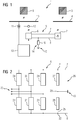
- FIG. 1 an installation 1 for transmitting electrical power is shown.
- the system 1 comprises a diode rectifier 2.
- the diode rectifier 2 is connected on the AC voltage side via a busbar 4 to a three-phase first AC voltage network 3.
- the diode rectifier 2 is connected on the DC voltage side via a DC voltage connection 5 to a modular multi-stage converter (MMC) 6.
- the DC voltage connection 5 comprises a first DC voltage pole 7 and a second DC voltage pole 8.
- the first DC voltage pole 7 is a positive DC voltage pole
- the second DC voltage pole 8 is a negative DC voltage pole.
- the MMC 6 is connected on the DC voltage side to the DC voltage connection 5 and on the AC voltage side via a busbar 10 to a three-phase second AC voltage network 9.
- the system 1 also includes a voltage measuring unit 11 and a current measuring unit 12 as well as a control unit 13 for regulating and activating the MMC 6.
- a filter unit 14 On the DC voltage side of the MMC 6, a filter unit 14 is provided which is set up to filter an AC voltage component in the DC power that is between the Diode rectifier 2 and the MMC 6 is transmitted.
- the filter unit 14 connects the MMC 6 via the second DC voltage pole 8 of the DC voltage connection 5 to a neutral point 15, which in the example shown is a ground connection.
- the filter unit 14 comprises a passive filter 16.
- FIG 2 shows a modular multi-stage converter (MMC) 6 for the system 1 of Figure 1 .
- MMC modular multi-stage converter
- the MMC 6 has a first DC voltage pole 21 and a second DC voltage pole 22.
- the first DC voltage pole 21 is connected to the first DC voltage pole 7 of the DC voltage connection 5.
- the second DC voltage pole 22 is correspondingly connected to the second DC voltage pole 8 of the DC voltage connection 5.
- the MMC 6 also has an AC voltage connection 23, which is set up to connect the MMC 6 to the three-phase AC voltage network 9. Between each of the two DC voltage poles 21, 22 and the AC voltage connection 23, six phase branches 24 of the same structure extend. The structure of a phase branch 24 is shown below in FIG Figure 5 detailed.
- a branch 25 of a filter unit extends between the first and the second DC voltage pole 21 and 22, respectively.
- the filter unit 26 comprises a first filter 27 and a second filter 28, which are arranged in series with one another.
- a potential point 29 between the two filters 27 and 28 is connected to the ground connection 15, which represents the neutral point of the AC voltage network 9.
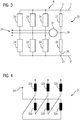
- FIG 3 shows the MMC 6 with a filter unit 30.
- the filter unit 30 is largely the same as the filter unit 26 of FIG Figure 2 with the difference that the potential point 29 between the filters 27 and 28 of the filter unit 30 with a star point (in Figure 3 not shown in the figure) of a grounding transformer 31 is connected.
- the star point of the grounding transformer 31 represents the neutral point of the AC voltage network 9.
- the structure of the grounding transformer 31 known to those skilled in the art is shown below Figure 4 shown in more detail.
- the grounding transformer 31 comprises a first, a second and a third primary winding 32a, 32b, 32c, which are connected to the AC voltage connection 23 of the MMC 6.
- the primary windings 32a-c are connected to compensation windings 33a-c in a zigzag arrangement.
- the compensation windings 33a-c are connected to a star point 34 of the grounding transformer 31.
- the star point 34 can be galvanically connected to the potential point 29 of the filter unit.
- phase branch 24 of the MMC 6 is shown.
- the in Figure 5 The phase branch 24 shown extends between the first DC voltage pole 7 and the AC voltage connection 23 of the MMC 6.
- the phase branch 24 comprises a current measuring element 35 for measuring a branch current Iz as well as a series connection of similarly constructed two-pole switching modules 36.
- the number of switching modules 36 is basically arbitrary and depending on the respective application adapted what is in Figure 5 is indicated by the broken line 37.
- a smoothing choke 38 is arranged in a series connection with the switching modules 36. The structure of the switching modules 36 is described in the following Figures 7 and 8 detailed.
- FIG Figure 6 shows the structure of a filter 27 of the filter units 26 and 30.
- the filter 27 can also be used as a filter 16 of the filter unit 14 of FIG Figure 1 can be used.
- the filter 27 comprises a series connection of a filter capacitor 41 and a filter choke 42.
- the dimensioning and design of the capacitance C of the filter capacitor 41 and the inductance L of the filter choke 42 can be adapted to the respective application.
- C and L are adapted to a network frequency of the AC voltage network connected to the MMC 6 in such a way that this corresponds to the resonance frequency of the filter 27.
- a single filter choke and a single filter capacitor several chokes and / or capacitors connected in series or in parallel can also be provided.
- the second filter 28 of the filter units 26 and 30 is constructed in the same way as the filter 27, it also being possible for the arrangement of the filter capacitor 41 and the filter choke 42 to be interchanged.
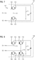
- FIG. 7 shows in detail a switching module in the form of a half-bridge circuit 101.
- the half-bridge circuit 101 has two connections X1 and X2.
- the connection X1 can, for example, connect the half-bridge circuit 101 to the connection X2 of a further half-bridge circuit, so that a series connection of the submodules is formed.
- the half-bridge circuit 101 comprises a first semiconductor switch 102 in the form of a bipolar transistor with an insulated gate electrode (IGBT), to which a freewheeling diode 103 is connected in anti-parallel.
- the half-bridge circuit 101 furthermore comprises a second semiconductor switch 104 in the form of an IGBT to which a freewheeling diode 105 is connected in anti-parallel.
- the forward direction of the two semiconductor switches 102 and 104 is rectified.
- the first connection X1 is arranged at a potential point 113 between the two semiconductor switches 102 and 104.
- the second connection X2 is connected to the emitter of the second semiconductor switch 104.
- An energy store in the form of a power capacitor 106 is arranged parallel to the two semiconductor switches 102, 104. With a suitable control of the semiconductor switches 102, 104, the capacitor 106 can be switched on or bridged with an operating current direction indicated by an arrow 107, so that either the voltage Uc dropping across the capacitor 106 or a voltage zero drops at the connections X1, X2.
- FIG Figure 8 An example of a switching module in the form of a full bridge circuit 108 is shown in FIG Figure 8 shown schematically.
- the full bridge circuit 108 has a first semiconductor switch 102 in the form of an IGBT, to which a freewheeling diode 103 is connected in anti-parallel, and a second semiconductor switch 104 in the form of an IGBT, to which a freewheeling diode 105 is connected in anti-parallel.
- the forward direction of the two semiconductor switches 102 and 104 is rectified.
- the full bridge circuit 108 comprises a third semiconductor switch 109 in the form of an IGBT, to which a freewheeling diode 110 is connected in anti-parallel, and a fourth semiconductor switch 111 in the form of an IGBT, to which a freewheeling diode 112 is connected in anti-parallel.
- the forward direction of the two semiconductor switches 109 and 111 is rectified.
- the semiconductor switches 102 and 104 with their associated freewheeling diodes 103, 105 thus form a series circuit that is connected in parallel to a series circuit formed by the semiconductor switches 109, 111 and the associated freewheeling diodes 110 and 112.
- An energy store in the form of a power capacitor 106 is arranged in parallel to the two series connections.
- the first connection X1 is arranged at a potential point 113 between the semiconductor switches 102, 104
- the second connection X2 is arranged at a potential point 114 between the semiconductor switches 109, 111.
- the voltage drop across the terminals X1, X2 can be generated, which corresponds to the voltage Uc dropping across the capacitor 106, the voltage dropping across the capacitor 106 but with opposite polarity or the voltage zero .
Description
- Die Erfindung betrifft eine Anlage zum Übertragen elektrischer Leistung mit einem unidirektionalen Gleichrichter, der wechselspannungsseitig mit einem ersten Wechselspannungsnetz verbindbar ist, einem selbstgeführten Umrichter, der wechselspannungsseitig mit einem zweiten Wechselspannungsnetz verbindbar ist, sowie mit einer Gleichspannungsverbindung, die den Gleichrichter und den Umrichter gleichspannungsseitig miteinander verbindet Die Erfindung betrifft außerdem einen modularen Mehrstufenumrichter.
- Eine solche Anlage ist beispielsweise aus der
US 8 120 202 B2 bekannt. Bei der bekannten Anlage sind Windkraftanlagen eines Windparks an das erste Wechselspannungsnetz angeschlossen. - Die von den Windkraftanlagen erzeugte elektrische Leistung wird mittels der bekannten Anlage an ein mit der Umrichteranlage verbundenes Versorgungsnetz übertragen.
- Mittels des unidirektionalen Gleichrichters ist eine Leistungsübertragung lediglich in eine Richtung möglich. Dies führt insbesondere dazu, dass bei einer Auslegung des selbstgeführten Umrichters der Umstand berücksichtigt werden muss, dass das erste Wechselspannungsnetz unter Umständen nicht symmetrisch ist. Eine Unsymmetrie des ersten Wechselspannungsnetzes kann beispielsweise durch einen Netzfehler oder einen unsymmetrischen Betrieb von Generatoren oder Motoren entstehen. Die Unsymmetrie des ersten Wechselspannungsnetzes kann Spannungsschwankungen im selbstgeführten Umrichter bewirken, die bei dessen Auslegung zu berücksichtigen sind. Eine entsprechende höhere Auslegung des selbstgeführten Umrichters kann nachteilig die Kosten der Anlage erhöhen.
- Die
EP 2 713 494 A1 offenbart eine Anordnung mit einem Gleichstrom-Filter am Gleichstromkreis. Die Aufgabe des Gleichstromfilters ist es, den Gleichstromkreis gegen elektromagnetische Einflüsse einer angeschlossenen Energieeinspeisevorrichtung zu isolieren, um elektromagnetische Verträglichkeit zu gewährleisten. - Aus der
WO 2007/028350 A1 ist eine Anordnung von Umrichtern mit einem Filter zur zusätzlichen Glättung der Gleichspannung bekannt Ein modularer Mehrstufenumrichter ist beispielsweise aus dem DokumentDE 10 103 031 A1 als bekannt zu entnehmen. Eine Filteranordnung zur Filterung und Bedämpfung von Oberschwingungen oder höherfrequenten Schwingungspaketen und zur Verschiebung von Resonanzstellen in elektrischen Netzen ist aus dem DokumentWO 91/09451 A1 - Aufgabe der Erfindung ist es, eine eingangs genannte Anlage vorzuschlagen, die möglichst kostengünstig ist.
- Diese Aufgabe wird erfindungsgemäß durch die Anlage mit den Merkmalen des Anspruchs 1 gelöst. Vorteilhafte Ausgestaltungen der Erfindung sind Gegenstand der abhängigen Ansprüche.
- Die Aufgabe wird bei einer artgemäßen Anlage durch eine gleichspannungsseitig mit dem Umrichter verbundene Filtereinheit gelöst, die einen Strompfad zu einem Neutralpunkt des zweiten Wechselspannungsnetzes ausbildet, wobei der Strompfad eine hohe Impedanz für einen Gleichstrom und eine niedrige Impedanz für einen Wechselstrom mit der Grundschwingungsfrequenz des zweiten Wechselspannungsnetzes aufweist. Der Strompfad der Filtereinheit kann sich dabei beispielsweise zwischen einem Gleichspannungspol des Umrichters bzw. der Gleichspannungsverbindung und dem Neutralpunkt erstrecken. Mittels der Filtereinheit wird also die Gleichspannungsseite des Umrichters an den Neutralpunkt angeschlossen. Mit anderen Worten kann die Filtereinheit zumindest einen Gleichspannungspol des Umrichters mit dem Neutralpunkt verbinden. Aufgrund der hohen Impedanz für Gleichströme findet gleichspannungsseitig des Umrichters kein Spannungsverlust statt. Die hohe Impedanz für Gleichströme lässt sich beispielsweise durch eine Potenzialtrennung realisieren, zweckmäßigerweise mittels einer kapazitiven Potenzialtrennung. Die niedrige Impedanz der Filtereinheit für netzfrequente Wechselströme bedeutet, dass Wechselspannungsanteile einer Spannung auf der Gleichspannungsseite des Umrichters an den Neutralpunkt kurzgeschlossen werden, insbesondere diejenigen mit der Grundschwingungsfrequenz des Wechselspannungsnetzes. Auf diese Weise können die durch eine Unsymmetrie des ersten Wechselspannungsnetzes bewirkten Spannungsschwankungen im Umrichter vorteilhaft verringert oder gar vermieden werden. Dies senkt vorteilhaft die Kosten der gesamten Anlage.
- Der Neutralpunkt stellt eine Anbindung an ein festes Potenzial dar. Die Potenzialanbindung kann bezüglich eines der beiden Wechselspannungsnetze erfolgen.
- Gemäß der Erfindung ist der Neutralpunkt ein Sternpunkt eines mit dem zweiten Wechselspannungsnetz verbundenen Sternpunkttransformators in Zickzackwicklung, der im Folgenden auch als Erdungstransformator bezeichnet wird. Demnach erstreckt sich der Strompfad der Filtereinheit beispielsweise zwischen einem der Gleichspannungspole des Umrichters bzw. der Gleichspannungsverbindung und dem Sternpunkt des Erdungstransformators. Dies ist besonders vorteilhaft, wenn die Filtereinheit in der räumlichen Nähe des Umrichters angeordnet ist, so dass die Anbindung an das zweite Wechselspannungsnetz nicht aufwändig ist.
- Vorteilhafterweise umfasst die Filtereinheit ausschließlich passive Filterkomponenten. Passive Filterkomponenten sind besonders günstig in Montage und Betrieb, insbesondere weil sie keine Regelung erfordern. Eine passive Filterkomponente kann beispielsweise eine Drossel, eine Kapazität in Form eines Kondensators, ein Widerstandselement oder auch eine Kombination dieser oder ähnlicher Komponenten sein.
- Gemäß der Erfindung umfasst die Filtereinheit eine Reihenschaltung einer Induktivität und einer Kapazität. Die Filtereinheit bildet somit einen Saugkreis, der die Wechselspannungsanteile bei geeigneter Auslegung herausfiltern kann. Die Induktivität ist beispielsweise eine Filterdrossel, die Kapazität entsprechend ein Filterkondensator.
- Erfindungsgemäß sind die Kapazität und die Induktivität derart ausgelegt, dass eine Resonanzfrequenz der Filtereinheit auf die Betriebsfrequenz bzw. Grundschwingungsfrequenz des zweiten Wechselspannungsnetzes abgestimmt ist. Auf diese Weise ist eine besonders niedrige Impedanz für den Wechselstrom mit der Grundschwingungsfrequenz des Wechselspannungsnetzes und damit eine besonders wirksame Filterung bereitgestellt. Bekannterweise gilt in einem solchen Fall beispielsweise für die Induktivität L einer Filterdrossel und die Kapazität C eines Filterkondensators, dass f = 1 / (2 * Pi * (L * C)^(1/2)), wobei f die Resonanzfrequenz der Filtereinheit bezeichnet.
- Gemäß einer Ausführungsform der Erfindung umfasst die Filtereinheit einen Stromzweig, der sich zwischen einem positiven Gleichspannungspol des Umrichters und einem negativen Gleichspannungspol des Umrichters erstreckt, wobei der Stromzweig einen ersten Filter mit einer Reihenschaltung einer ersten Induktivität und einer ersten Kapazität sowie einen zweiten Filter mit einer Reihenschaltung mit einer zweiten Induktivität und einer zweiten Kapazität umfasst, wobei ein Potenzialpunkt zwischen dem ersten und dem zweiten Filter mit dem Neutralpunkt verbunden ist. Der Stromzweig kann sich entsprechend auch zwischen einem ersten und einem zweiten Gleichspannungspol der Gleichspannungsleitung erstrecken. Somit umfasst die Filtereinheit zwei Teilfilter. Der erste Teilfilter ist zwischen dem ersten Gleichspannungspol des Umrichters bzw. der Gleichspannungsverbindung und dem Neutralpunkt angeordnet. Der zweite Teilfilter ist zwischen dem Neutralpunkt und dem zweiten Gleichspannungspol des Umrichters bzw. der Gleichspannungsverbindung angeordnet. Auf diese Weise ist eine besonders wirksame Filterung der Wechselspannungsanteile in der Gleichspannung realisiert.
- Vorzugsweise ist der unidirektionale Gleichrichter ein Diodengleichrichter. Diodengleichrichter sind besonders einfach und robust in Betrieb. Zugleich sind sie beispielsweise gegenüber selbstgeführten Umrichtern vergleichsweise kompakt und gewichtsarm. Zudem ist der Diodengleichrichter relativ verlustarm im Betrieb. Der Diodengleichrichter kann zum Beispiel als eine Sechspulseine Zwölfpuls oder eine 24-Puls-Brücke realisiert sein.
- Gemäß einer Ausführungsform der Erfindung ist der selbstgeführte Umrichter ein modularer Mehrstufenumrichter (MMC). Der modulare Mehrstufenumrichter zeichnet sich durch eine modulare Bauweise aus. Der modulare Mehrstufenumrichter umfasst Phasenzweige, die sich jeweils zwischen einem Wechselspannungsanschluss des Mehrstufenumrichters und einem der beiden Gleichspannungspole erstrecken. Die Phasenzweige des modularen Mehrstufenumrichters weisen jeweils eine Reihenschaltung zweipoliger Schaltmodule auf, wobei jedes Schaltmodul ein- und abschaltbare Leistungshalbleiterschalter sowie einen Energiespeicher, bevorzugt in Form eines Kondensators, umfasst. Ferner ist jedes der Schaltmodule einzeln ansteuerbar. Eine an dem Phasenzweig abfallende Spannung ist gleich der Summe von Spannungen, die an den zugehörigen Schaltmodulen abfallen. Mittels des MMC ist eine besonders vorteilhafte stufenförmige Konverterspannung erzeugbar. Ein MMC ist beispielsweise in der
DE 101 03 031 B4 beschrieben. Bevorzugt sind die Schaltmodule als Halbbrückenschaltungen oder als Vollbrückenschaltungen ausgebildet. Gemäß einer Ausführungsvariante der Erfindung weist jedes Schaltmodul eine Vollbrückenschaltung mit vier abschaltbaren Leistungshalbleitern und einem Energiespeicher auf, die so mit dem Energiespeicher verschaltet sind, dass an Ausgangsklemmen des Schaltmoduls eine an dem Energiespeicher abfallende Energiespeicherspannung, eine Nullspannung oder aber die inverse Energiespeicherspannung erzeugbar ist. Gemäß einer weiteren Ausführungsvariante weist jedes Schaltmodul eine Halbbrückenschaltung mit zwei abschaltbaren Leistungshalbleitern und einem Energiespeicher auf, die so mit dem Energiespeicher verschaltet sind, dass an Ausgangsklemmen des Schaltmoduls eine an dem Energiespeicher abfallende Energiespeicherspannung oder eine Nullspannung erzeugbar ist. Ferner ist es ebenfalls denkbar, dass einige der Schaltmodule des MMC Vollbrückenschaltungen und einige weitere Schaltmodule Halbbrückenschaltungen aufweisen. - Die Verwendung eines MMC in der erfindungsgemäßen Anlage ist besonders vorteilhaft. Die Bereitstellung der Filtereinheit ermöglicht eine Verringerung der Anzahl der im MMC verbauten Schaltmodule in jedem Phasenzweig. Dies erlaubt eine vorteilhafte Senkung der Kosten des MMC und der gesamten Anlage, weil die Schaltmodule relativ kostenintensive Bauteile sind. Zudem sind durch die Verringerung der Anzahl der Schaltmodule in jedem Phasenzweig die elektrischen Verluste der Anlage gesenkt, was die Betriebskosten der Anlage weiter senkt.
- Die Erfindung betrifft ferner einen modularen Mehrstufenumrichter, der wechselspannungsseitig mit einem Wechselspannungsnetz und gleichspannungsseitig mit einer Gleichspannungsverbindung verbindbar ist.
- Die Aufgabe der Erfindung besteht darin, einen solchen modularen Mehrstufenumrichter bereitzustellen, der möglichst kostengünstig ist.
- Die Aufgabe wird bei einem artgemäßen modularen Mehrstufenumrichter durch die Merkmale des Anspruchs 6 gelöst.
- Die Vorteile des erfindungsgemäßen modularen
- Mehrstufenumrichters ergeben sich insbesondere aus den zuvor beschriebenen Vorteilen der erfindungsgemäßen Anlage zum Übertragen elektrischer Leistung.
- Alle im Zusammenhang mit der erfindungsgemäßen Anlage beschriebenen Merkmale und Ausführungsvarianten der Filtereinheit bzw. des Umrichters können selbstverständlich auch einzeln oder in Kombination mit dem erfindungsgemäßen modularen Mehrstufenumrichter verwirklicht werden.
- Die Erfindung soll im Folgenden anhand der
Figuren 1 bis 8 weiter erläutert werden. -
Figur 1 zeigt ein Beispiel einer vorliegend nicht beanspruchten Anlage zum Übertragen elektrischer Leistung in einer schematischen Darstellung; -
Figur 2 zeigt ein Beispiel eines vorliegend nicht beanspruchten modularen Mehrstufenumrichters in einer schematischen Darstellung; -
Figur 3 zeigt ein Ausführungsbeispiel eines erfindungsgemäßen modularen Mehrstufenumrichters in einer schematischen Darstellung; -
Figur 4 zeigt ein Beispiel eines Erdungstransformators in einer schematischen Darstellung; -
Figur 5 zeigt ein Beispiel eines Phasenzweigs eines modularen Mehrstufenumrichters in einer schematischen Darstellung; -
Figur 6 zeigt ein Beispiel einer Filtereinheit in einer schematischen Darstellung; -
Figur 7 zeigt ein erstes Beispiel eines Schaltmoduls eines modularen Mehrstufenumrichters in einer schematischen Darstellung; -
Figur 8 zeigt ein zweites Beispiel eines Schaltmoduls eines modularen Mehrstufenumrichters in einer schematischen Darstellung. - Im Einzelnen ist in
Figur 1 eine Anlage 1 zum Übertragen elektrischer Leistung dargestellt. Die Anlage 1 umfasst einen Diodengleichrichter 2. Der Diodengleichrichter 2 ist wechselspannungsseitig über eine Sammelschiene 4 mit einem dreiphasigen ersten Wechselspannungsnetz 3 verbunden. Ferner ist der Diodengleichrichter 2 gleichspannungsseitig über eine Gleichspannungsverbindung 5 mit einem modularen Mehrstufenumrichter (MMC) 6 verbunden. Die Gleichspannungsverbindung 5 umfasst einen ersten Gleichspannungspol 7 und einen zweiten Gleichspannungspol 8. Im dargestellten Beispiel ist der erste Gleichspannungspol 7 ein positiver Gleichspannungspol und der zweite Gleichspannungspol 8 ein negativer Gleichspannungspol. - Der MMC 6 ist gleichspannungsseitig mit der Gleichspannungsverbindung 5 und wechselspannungsseitig über eine Sammelschiene 10 mit einem dreiphasigen zweiten Wechselspannungsnetz 9 verbunden.
- Die Anlage 1 umfasst ferner eine Spannungsmesseinheit 11 und eine Strommesseinheit 12 sowie eine Steuereinheit 13 zum Regeln und Ansteuern des MMC 6.
- Gleichspannungsseitig des MMC 6 ist eine Filtereinheit 14 vorgesehen, die zum Filtern eines Wechselspannungsanteils in der DC-Leistung eingerichtet ist, die zwischen dem Diodengleichrichter 2 und dem MMC 6 übertragen wird. Die Filtereinheit 14 verbindet den MMC 6 über den zweiten Gleichspannungspol 8 der Gleichspannungsverbindung 5 mit einem Neutralpunkt 15, der im dargestellten Beispiel eine Erdanbindung ist. Die Filtereinheit 14 umfasst einen passiven Filter 16.
-
Figur 2 zeigt einen modularen Mehrstufenumrichter (MMC) 6 für die Anlage 1 derFigur 1 . Gleiche und gleichartige Elemente wurden dabei in denFiguren 1 und 2 mit gleichen Bezugszeichen versehen. Entsprechendes gilt auch für die nachfolgendenFiguren 3 bis 8 . - Der MMC 6 weist einen ersten Gleichspannungspol 21 und einen zweiten Gleichspannungspol 22. Der erste Gleichspannungspol 21 ist mit dem ersten Gleichspannungspol 7 der Gleichspannungsverbindung 5 verbunden. Entsprechend ist der zweite Gleichspannungspol 22 mit dem zweiten Gleichspannungspol 8 der Gleichspannungsverbindung 5 verbunden. Der MMC 6 weist ferner einen Wechselspannungsanschluss 23 auf, der zum Anschluss des MMC 6 an das dreiphasige Wechselspannungsnetz 9 eingerichtet ist. Zwischen jedem der beiden Gleichspannungspole 21, 22 und dem Wechselspannungsanschluss 23 erstrecken sich sechs gleichartig aufgebaute Phasenzweige 24. Auf den Aufbau eines Phasenzweiges 24 wird nachfolgend in
Figur 5 näher eingegangen. - Zwischen dem ersten und dem zweiten Gleichspannungspol 21 bzw. 22 erstreckt sich ein Stromzweig 25 einer Filtereinheit 26. Die Filtereinheit 26 umfasst einen ersten Filter 27 und einen zweiten Filter 28, die in Reihe zueinander angeordnet sind. Ein Potenzialpunkt 29 zwischen den beiden Filtern 27 bzw. 28 ist mit dem Erdanschluss 15 verbunden, der den Neutralpunkt des Wechselspannungsnetzes 9 darstellt.
-
Figur 3 zeigt den MMC 6 mit einer Filtereinheit 30. Die Filtereinheit 30 gleicht weitgehend der Filtereinheit 26 derFigur 2 mit dem Unterschied, dass der Potenzialpunkt 29 zwischen den Filtern 27 und 28 der Filtereinheit 30 mit einem Sternpunkt (inFigur 3 figürlich nicht dargestellt) eines Erdungstransformators 31 verbunden ist. Gemäß diesem Ausführungsbeispiel stellt der Sternpunkt des Erdungstransformators 31 den Neutralpunkt des Wechselspannungsnetzes 9 dar. - Der Aufbau des dem Fachmann bekannten Erdungstransformators 31 ist in der nachfolgenden
Figur 4 näher dargestellt. Der Erdungstransformator 31 umfasst eine erste, eine zweite und eine dritte Primärwicklung 32a, 32b, 32c, die mit dem Wechselspannungsanschluss 23 des MMC 6 verbunden sind. Die Primärwicklungen 32a-c sind mit Kompensationswicklungen 33a-c in einer Zickzack-Anordnung verbunden. Die Kompensationswicklungen 33a-c sind zu einem Sternpunkt 34 des Erdungstransformators 31 verschaltet. Der Sternpunkt 34 kann mit dem Potenzialpunkt 29 der Filtereinheit galvanisch verbunden werden. - In
Figur 5 ist ein Phasenzweig 24 des MMC 6 dargestellt. Der inFigur 5 gezeigte Phasenzweig 24 erstreckt sich zwischen dem ersten Gleichspannungspol 7 und dem Wechselspannungsanschluss 23 des MMC 6. Der Phasenzweig 24 umfasst eine Strommesselement 35 zum Messen eines Zweigstromes Iz sowie eine Reihenschaltung gleichartig aufgebauter zweipoliger Schaltmodule 36. Die Anzahl der Schaltmodule 36 ist grundsätzlich beliebig und auf die jeweilige Anwendung angepasst, was inFigur 5 durch die unterbrochene Linie 37 angedeutet ist. In einer Reihenschaltung zu den Schaltmodulen 36 ist eine Glättungsdrossel 38 angeordnet. Auf den Aufbau der Schaltmodule 36 wird in den nachfolgendenFiguren 7 und 8 näher eingegangen. -
Figur 6 zeigt den Aufbau eines Filters 27 der Filtereinheiten 26 und 30. Der Filter 27 kann mit gleichem Aufbau auch als Filter 16 der Filtereinheit 14 derFigur 1 eingesetzt werden. Der Filter 27 umfasst eine Reihenschaltung aus einem Filterkondensator 41 und einer Filterdrossel 42. Die Bemessung und Auslegung der Kapazität C des Filterkondensators 41 und die Induktivität L der Filterdrossel 42 können an die jeweilige Anwendung angepasst sein. Insbesondere sind C und L auf eine Netzfrequenz des mit dem MMC 6 verbundenen Wechselspannungsnetzes derart angepasst, dass diese der Resonanzfrequenz des Filters 27 entspricht. Anstelle einer einzelnen Filterdrossel und eines einzelnen Filterkondensators können auch mehrere in Reihe oder parallel geschaltete Drosseln und/oder Kondensatoren vorgesehen sein. - Der zweite Filter 28 der Filtereinheiten 26 bzw. 30 ist zum Filter 27 gleichartig aufgebaut, wobei die Anordnung des Filterkondensators 41 und der Filterdrossel 42 auch vertauscht sein kann.
- In den nachfolgenden
Figuren 7 und 8 sind zwei Ausführungsbeispiele der Schaltmodule 36 der Phasenzweige 24 des MMC 6 dargestellt. -
Figur 7 zeigt im Einzelnen ein Schaltmodul in Form einer Halbbrückenschaltung 101. Die Halbbrückenschaltung 101 weist zwei Anschlüsse X1 und X2 auf. Der Anschluss X1 kann beispielsweise die Halbbrückenschaltung 101 mit dem Anschluss X2 einer weiteren Halbbrückenschaltung verbinden, so dass eine Reihenschaltung der Submodule gebildet wird. - Die Halbbrückenschaltung 101 umfasst einen ersten Halbleiterschalter 102 in Form eines Bipolartransistors mit isolierter Gate-Elektrode (IGBT), dem eine Freilaufdiode 103 antiparallel geschaltet ist. Ferner umfasst die Halbbrückenschaltung 101 einen zweiten Halbleiterschalter 104 in Form eines IGBT, dem eine Freilaufdiode 105 antiparallel geschaltet ist. Die Durchlassrichtung der beiden Halbleiterschalter 102 und 104 ist gleichgerichtet. Der erste Anschluss X1 ist an einem Potenzialpunkt 113 zwischen den beiden Halbleiterschaltern 102 und 104 angeordnet. Der zweite Anschluss X2 ist mit dem Emitter des zweiten Halbleiterschalters 104 verbunden.
- Parallel zu den beiden Halbleiterschaltern 102, 104 ist ein Energiespeicher in Form eines Leistungskondensators 106 angeordnet. Durch eine geeignete Ansteuerung der Halbleiterschalter 102, 104 kann, bei einer durch einen Pfeil 107 angedeuteten Betriebsstromrichtung, der Kondensator 106 zugeschaltet oder überbrückt werden, so dass an den Anschlüssen X1, X2 entweder die am Kondensator 106 abfallende Spannung Uc oder eine Spannung null abfällt.
- Ein Beispiel eines Schaltmoduls in Form einer Vollbrückenschaltung 108 ist in
Figur 8 schematisch dargestellt. Die Vollbrückenschaltung 108 weist einen ersten Halbleiterschalter 102 in Form eines IGBT, dem eine Freilaufdiode 103 antiparallel geschaltet ist sowie einen zweiten Halbleiterschalter 104 in Form eines IGBT, dem eine Freilaufdiode 105 antiparallel geschaltet ist. Die Durchlassrichtung der beiden Halbleiterschalter 102 und 104 ist gleichgerichtet. Ferner umfasst die Vollbrückenschaltung 108 einen dritten Halbleiterschalter 109 in Form eines IGBT, dem eine Freilaufdiode 110 antiparallel geschaltet ist sowie einen vierten Halbleiterschalter 111 in Form eines IGBT, dem eine Freilaufdiode 112 antiparallel geschaltet ist. Die Durchlassrichtung der beiden Halbleiterschalter 109 und 111 ist gleichgerichtet. Die Halbleiterschalter 102 und 104 mit ihnen zugeordneten Freilaufdioden 103, 105 bilden somit eine Reihenschaltung, die einer durch die Halbleiterschalter 109, 111 und die zugeordneten Freilaufdioden 110 und 112 gebildeten Reihenschaltung parallel geschaltet ist. Ein Energiespeicher in Form eines Leistungskondensators 106 ist parallel zu den beiden Reihenschaltungen angeordnet. Der erste Anschluss X1 ist an einem Potenzialpunkt 113 zwischen den Halbleiterschaltern 102, 104 angeordnet, der zweite Anschluss X2 ist an einem Potenzialpunkt 114 zwischen den Halbleiterschaltern 109, 111 angeordnet. - Durch eine geeignete Steuerung der Leistungshalbleiter 102, 104, 109 und 111 kann die an den Anschlüssen X1, X2 abfallende Spannung erzeugt werden, die der am Kondensator 106 abfallenden Spannung Uc, der am Kondensator 106 abfallenden Spannung jedoch mit entgegengesetzter Polarität oder der Spannung null entspricht.
Claims (6)
- Anlage (1) zum Übertragen elektrischer Leistung mit- einem unidirektionalen Gleichrichter (2), der wechselspannungsseitig mit einem ersten Wechselspannungsnetz (3) verbindbar ist,- einem selbstgeführten Umrichter (6), der wechselspannungsseitig mit einem zweiten Wechselspannungsnetz (9) verbindbar ist,- einer Gleichspannungsverbindung (5), die den Gleichrichter (2) und den Umrichter (6) gleichspannungsseitig miteinander verbindet, wobei die Anlage weiterhin eine gleichspannungsseitig mit dem Umrichter (6) verbundene Filtereinheit (30) aufweist, die einen Strompfad zu einem Neutralpunkt (34) ausbildet, wobei der Strompfad eine hohe Impedanz für einen Gleichstrom und eine niedrige Impedanz für einen Wechselstrom mit der Grundschwingungsfrequenz des zweiten Wechselspannungsnetzes (9) aufweist, dadurch gekennzeichnet, dass die Filtereinheit (30) eine Reihenschaltung einer Induktivität (42) und einer Kapazität (41) umfasst, wobei die Kapazität (41) und die Induktivität (42) derart ausgelegt sind, dass eine Resonanzfrequenz der Filtereinheit (30) auf eine Betriebsfrequenz des zweiten Wechselspannungsnetzes (9) abgestimmt ist, wobei die Anlage einen Sternpunkttransformator (31) in Zickzackwicklung aufweist, der zum Verbinden mit dem zweiten Wechselspannungsnetz (9) vorgesehen ist, und wobei der Neutralpunkt durch einen Sternpunkt (34) des Sternpunkttransformators (31) gebildet ist.
- Anlage (1) nach Anspruch 1, wobei die Filtereinheit (30) ausschließlich passive Filterkomponenten (41, 42) umfasst.
- Anlage (1) nach einem der vorangehenden Ansprüche, wobei die Filtereinheit (30) einen Stromzweig (25) umfasst, der sich zwischen einem positiven Gleichspannungspol (21) des Umrichters (6) und einem negativen Gleichspannungspol (22) des Umrichters (6) erstreckt, wobei der Stromzweig (25) einen ersten Filter (27) mit einer Reihenschaltung einer ersten Induktivität (12) und einer ersten Kapazität (41) sowie einen zweiten Filter (28) mit einer Reihenschaltung mit einer zweiten Induktivität (42) und einer zweiten Kapazität (41) umfasst, wobei ein Potenzialpunkt (29) zwischen dem ersten und dem zweiten Filter (27, 28) mit dem Neutralpunkt (34) verbunden ist.
- Anlage (1) nach einem der vorangehenden Ansprüche, wobei der unidirektionale Gleichrichter (2) ein Diodengleichrichter ist.
- Anlage (1) nach einem der vorangehenden Ansprüche, wobei der selbstgeführte Umrichter (6) ein modularer Mehrstufenumrichter ist.
- Modularer Mehrstufenumrichter (6), der wechselspannungsseitig mit einem Wechselspannungsnetz (9) und gleichspannungsseitig mit einer Gleichspannungsverbindung (15) verbindbar ist,
wobei der Mehrstufenumrichter (6) eine mit einer Gleichspannungsseite des Mehrstufenumrichters (6) verbundene Filtereinheit (30) aufweist, die einen Strompfad zu einem Neutralpunkt (34) ausbildet, wobei der Strompfad eine hohe Impedanz für einen Gleichstrom und eine niedrige Impedanz für einen Wechselstrom mit der Grundschwingungsfrequenz des Wechselspannungsnetzes (9) aufweist, dadurch gekennzeichnet, dass die Filtereinheit (30) eine Reihenschaltung einer Induktivität (42) und einer Kapazität (41) umfasst, wobei die Kapazität (41) und die Induktivität (42) derart ausgelegt sind, dass eine Resonanzfrequenz der Filtereinheit (30) auf eine Betriebsfrequenz des zweiten Wechselspannungsnetzes (9) abgestimmt ist, wobei der Mehrstufenumrichter einen Sternpunkttransformator (31) in Zickzackwicklung aufweist, der zum Verbinden mit dem Wechselspannungsnetz (9) vorgesehen ist, und wobei der Neutralpunkt durch einen Sternpunkt (34) des Sternpunkttransformators (31) gebildet ist.
Applications Claiming Priority (1)
| Application Number | Priority Date | Filing Date | Title |
|---|---|---|---|
| PCT/EP2016/076798 WO2018082786A1 (de) | 2016-11-07 | 2016-11-07 | Anlage zum übertragen elektrischer leistung mit filtereinheit |
Publications (2)
| Publication Number | Publication Date |
|---|---|
| EP3513475A1 EP3513475A1 (de) | 2019-07-24 |
| EP3513475B1 true EP3513475B1 (de) | 2021-02-24 |
Family
ID=57326355
Family Applications (1)
| Application Number | Title | Priority Date | Filing Date |
|---|---|---|---|
| EP16797479.9A Active EP3513475B1 (de) | 2016-11-07 | 2016-11-07 | Anlage zum übertragen elektrischer leistung mit filtereinheit |
Country Status (2)
| Country | Link |
|---|---|
| EP (1) | EP3513475B1 (de) |
| WO (1) | WO2018082786A1 (de) |
Families Citing this family (2)
| Publication number | Priority date | Publication date | Assignee | Title |
|---|---|---|---|---|
| DE102019214545B4 (de) * | 2019-09-24 | 2022-01-27 | Siemens Energy Global GmbH & Co. KG | Stromrichter und Verfahren zu dessen Betrieb |
| CN113098244B (zh) * | 2021-04-07 | 2022-05-06 | 全球能源互联网研究院有限公司 | 一种mmc换流器的桥臂电抗单元 |
Citations (1)
| Publication number | Priority date | Publication date | Assignee | Title |
|---|---|---|---|---|
| WO1991009451A1 (de) * | 1989-12-07 | 1991-06-27 | Elin Energieversorgung Gesellschaft M.B.H. | Filteranordnung |
Family Cites Families (4)
| Publication number | Priority date | Publication date | Assignee | Title |
|---|---|---|---|---|
| DE10103031B4 (de) | 2001-01-24 | 2011-12-01 | Siemens Ag | Stromrichterschaltung mit verteilten Energiespeichern und Verfahren zur Steuerung einer derartigen Stromrichterschaltung |
| EP1922804A1 (de) * | 2005-09-09 | 2008-05-21 | Siemens Aktiengesellschaft | Vorrichtung für die elektroenergieübertragung |
| US8120202B2 (en) | 2010-10-25 | 2012-02-21 | General Electric Company | Electric power transmission system for wind turbine and wind turbine farm and method for operating same |
| EP2713494A1 (de) * | 2012-09-28 | 2014-04-02 | Siemens Aktiengesellschaft | Energieeinspeisevorrichtung zur Einspeisung von aus kinetischer Energie erzeugter elektrischer Energie in ein Drehstromverteilernetz |
-
2016
- 2016-11-07 EP EP16797479.9A patent/EP3513475B1/de active Active
- 2016-11-07 WO PCT/EP2016/076798 patent/WO2018082786A1/de unknown
Patent Citations (1)
| Publication number | Priority date | Publication date | Assignee | Title |
|---|---|---|---|---|
| WO1991009451A1 (de) * | 1989-12-07 | 1991-06-27 | Elin Energieversorgung Gesellschaft M.B.H. | Filteranordnung |
Also Published As
| Publication number | Publication date |
|---|---|
| WO2018082786A1 (de) | 2018-05-11 |
| EP3513475A1 (de) | 2019-07-24 |
Similar Documents
| Publication | Publication Date | Title |
|---|---|---|
| EP3172823B1 (de) | Gleichspannungswandler mit transformator | |
| EP2432109B1 (de) | Modularer Schalter für einen elektrischen Umrichter, elektrischer Umrichter sowie Verfahren zum Betreiben eines elektrischen Umrichters | |
| EP2237404B1 (de) | Wechselrichter mit zwei asymmetrischen brückenschaltungen und einem freilaufpfad zur entkopplung von gleich- und wechselspannungsseite | |
| EP2107672A1 (de) | Dreiphasiger Wechselrichter ohne Verbindung zwischen dem Neutralleiter des Netzes und dem Mittelpunkt des Zwischenkreises | |
| DE102005019215B4 (de) | Ausgangsfilter für einen gepulsten Stromrichter | |
| EP2586646B1 (de) | Elektrische Energieversorgungsanordnung für Antriebseinrichtungen, zum Betreiben eines Schienenfahrzeugs an elektrischen Versorgungsnetzen | |
| WO2014206704A1 (de) | Umrichteranordnung mit parallel geschalteten mehrstufen-umrichtern sowie verfahren zu deren steuerung | |
| DE102011086087A1 (de) | Elektrischer Umrichter | |
| EP2845303A1 (de) | Stromrichter und betriebsverfahren zum wandeln von spannungen | |
| EP0682401B1 (de) | Einrichtung zur Begrenzung der Änderungsgeschwindigkeit der ausgangsseitigen Spannung eines selbstgeführten Umrichters | |
| CH693524A5 (de) | Einrichtung zur Begrenzung der Aenderungsgeschwindigkeit der Ausgangsgrössen eines über einen Gleichspannungszwischenkreis selbstgeführten mehrphasigen Umrichters. | |
| EP3245723A1 (de) | Gleichspannungswandler | |
| EP3513475B1 (de) | Anlage zum übertragen elektrischer leistung mit filtereinheit | |
| DE10303421A1 (de) | Strom-/Spannungswandleranordnung | |
| EP3652848B1 (de) | Resonanter gleichstromsteller | |
| WO2009098093A2 (de) | Wechselrichteranordnung zum einspeisen von photovoltaisch gewonnener energie in ein öffentliches netz | |
| EP0474060B1 (de) | Vierquadranten-Wechselstrom-Umrichter | |
| EP3098958B1 (de) | Spannungswandleranordnung mit kapazitiver kopplung | |
| EP3304718B1 (de) | Gleichspannungswandler für hohe spannungen | |
| EP3180844B1 (de) | Stromrichteranordnung mit kurzschlusseinheit sowie verfahren zum trennen einer wechselspannungsleitung | |
| DE4344709A1 (de) | Verfahren zur Umwandlung von unterschiedlich großen Gleich- oder Wechselspannungen in eine beliebig vorgegebene Spannung | |
| CH707447B1 (de) | Vorrichtung zur Gleichspannungswandlung für hohe Übersetzungsverhältnisse. | |
| EP3331118B1 (de) | Anlage zum übertragen elektrischer leistung | |
| WO2018113926A1 (de) | Stromrichter | |
| EP3526889B1 (de) | Umrichteranordnung mit sternpunktbildner |
Legal Events
| Date | Code | Title | Description |
|---|---|---|---|
| STAA | Information on the status of an ep patent application or granted ep patent |
Free format text: STATUS: UNKNOWN |
|
| STAA | Information on the status of an ep patent application or granted ep patent |
Free format text: STATUS: THE INTERNATIONAL PUBLICATION HAS BEEN MADE |
|
| PUAI | Public reference made under article 153(3) epc to a published international application that has entered the european phase |
Free format text: ORIGINAL CODE: 0009012 |
|
| STAA | Information on the status of an ep patent application or granted ep patent |
Free format text: STATUS: REQUEST FOR EXAMINATION WAS MADE |
|
| 17P | Request for examination filed |
Effective date: 20190412 |
|
| AK | Designated contracting states |
Kind code of ref document: A1 Designated state(s): AL AT BE BG CH CY CZ DE DK EE ES FI FR GB GR HR HU IE IS IT LI LT LU LV MC MK MT NL NO PL PT RO RS SE SI SK SM TR |
|
| AX | Request for extension of the european patent |
Extension state: BA ME |
|
| RIN1 | Information on inventor provided before grant (corrected) |
Inventor name: ALVAREZ VALENZUELA, RODRIGO ALONSO Inventor name: ANTES, ANDREAS Inventor name: PIESCHEL, MARTIN |
|
| DAV | Request for validation of the european patent (deleted) | ||
| DAX | Request for extension of the european patent (deleted) | ||
| STAA | Information on the status of an ep patent application or granted ep patent |
Free format text: STATUS: EXAMINATION IS IN PROGRESS |
|
| 17Q | First examination report despatched |
Effective date: 20200415 |
|
| GRAP | Despatch of communication of intention to grant a patent |
Free format text: ORIGINAL CODE: EPIDOSNIGR1 |
|
| STAA | Information on the status of an ep patent application or granted ep patent |
Free format text: STATUS: GRANT OF PATENT IS INTENDED |
|
| GRAJ | Information related to disapproval of communication of intention to grant by the applicant or resumption of examination proceedings by the epo deleted |
Free format text: ORIGINAL CODE: EPIDOSDIGR1 |
|
| STAA | Information on the status of an ep patent application or granted ep patent |
Free format text: STATUS: EXAMINATION IS IN PROGRESS |
|
| RIC1 | Information provided on ipc code assigned before grant |
Ipc: H02J 3/36 20060101ALN20200722BHEP Ipc: H02J 3/26 20060101ALI20200722BHEP Ipc: H02M 5/458 20060101ALI20200722BHEP Ipc: H02J 3/38 20060101ALN20200722BHEP Ipc: H02J 3/34 20060101ALI20200722BHEP Ipc: H02M 1/14 20060101ALI20200722BHEP Ipc: H02M 1/12 20060101AFI20200722BHEP Ipc: H02M 7/483 20070101ALN20200722BHEP |
|
| INTG | Intention to grant announced |
Effective date: 20200810 |
|
| REG | Reference to a national code |
Ref country code: DE Ref legal event code: R079 Ref document number: 502016012469 Country of ref document: DE Free format text: PREVIOUS MAIN CLASS: H02J0003260000 Ipc: H02M0001120000 |
|
| INTC | Intention to grant announced (deleted) | ||
| GRAP | Despatch of communication of intention to grant a patent |
Free format text: ORIGINAL CODE: EPIDOSNIGR1 |
|
| STAA | Information on the status of an ep patent application or granted ep patent |
Free format text: STATUS: GRANT OF PATENT IS INTENDED |
|
| RIC1 | Information provided on ipc code assigned before grant |
Ipc: H02M 1/14 20060101ALI20200910BHEP Ipc: H02J 3/36 20060101ALN20200910BHEP Ipc: H02J 3/34 20060101ALI20200910BHEP Ipc: H02M 7/483 20070101ALN20200910BHEP Ipc: H02J 3/26 20060101ALI20200910BHEP Ipc: H02M 5/458 20060101ALI20200910BHEP Ipc: H02M 1/12 20060101AFI20200910BHEP Ipc: H02J 3/38 20060101ALN20200910BHEP |
|
| INTG | Intention to grant announced |
Effective date: 20200929 |
|
| GRAS | Grant fee paid |
Free format text: ORIGINAL CODE: EPIDOSNIGR3 |
|
| GRAA | (expected) grant |
Free format text: ORIGINAL CODE: 0009210 |
|
| STAA | Information on the status of an ep patent application or granted ep patent |
Free format text: STATUS: THE PATENT HAS BEEN GRANTED |
|
| RAP1 | Party data changed (applicant data changed or rights of an application transferred) |
Owner name: SIEMENS ENERGY GLOBAL GMBH & CO. KG |
|
| AK | Designated contracting states |
Kind code of ref document: B1 Designated state(s): AL AT BE BG CH CY CZ DE DK EE ES FI FR GB GR HR HU IE IS IT LI LT LU LV MC MK MT NL NO PL PT RO RS SE SI SK SM TR |
|
| REG | Reference to a national code |
Ref country code: CH Ref legal event code: EP |
|
| REG | Reference to a national code |
Ref country code: DE Ref legal event code: R096 Ref document number: 502016012469 Country of ref document: DE |
|
| REG | Reference to a national code |
Ref country code: AT Ref legal event code: REF Ref document number: 1365737 Country of ref document: AT Kind code of ref document: T Effective date: 20210315 |
|
| REG | Reference to a national code |
Ref country code: IE Ref legal event code: FG4D Free format text: LANGUAGE OF EP DOCUMENT: GERMAN |
|
| REG | Reference to a national code |
Ref country code: LT Ref legal event code: MG9D |
|
| REG | Reference to a national code |
Ref country code: NL Ref legal event code: MP Effective date: 20210224 |
|
| PG25 | Lapsed in a contracting state [announced via postgrant information from national office to epo] |
Ref country code: FI Free format text: LAPSE BECAUSE OF FAILURE TO SUBMIT A TRANSLATION OF THE DESCRIPTION OR TO PAY THE FEE WITHIN THE PRESCRIBED TIME-LIMIT Effective date: 20210224 Ref country code: GR Free format text: LAPSE BECAUSE OF FAILURE TO SUBMIT A TRANSLATION OF THE DESCRIPTION OR TO PAY THE FEE WITHIN THE PRESCRIBED TIME-LIMIT Effective date: 20210525 Ref country code: HR Free format text: LAPSE BECAUSE OF FAILURE TO SUBMIT A TRANSLATION OF THE DESCRIPTION OR TO PAY THE FEE WITHIN THE PRESCRIBED TIME-LIMIT Effective date: 20210224 Ref country code: PT Free format text: LAPSE BECAUSE OF FAILURE TO SUBMIT A TRANSLATION OF THE DESCRIPTION OR TO PAY THE FEE WITHIN THE PRESCRIBED TIME-LIMIT Effective date: 20210624 Ref country code: NO Free format text: LAPSE BECAUSE OF FAILURE TO SUBMIT A TRANSLATION OF THE DESCRIPTION OR TO PAY THE FEE WITHIN THE PRESCRIBED TIME-LIMIT Effective date: 20210524 Ref country code: BG Free format text: LAPSE BECAUSE OF FAILURE TO SUBMIT A TRANSLATION OF THE DESCRIPTION OR TO PAY THE FEE WITHIN THE PRESCRIBED TIME-LIMIT Effective date: 20210524 Ref country code: LT Free format text: LAPSE BECAUSE OF FAILURE TO SUBMIT A TRANSLATION OF THE DESCRIPTION OR TO PAY THE FEE WITHIN THE PRESCRIBED TIME-LIMIT Effective date: 20210224 |
|
| PG25 | Lapsed in a contracting state [announced via postgrant information from national office to epo] |
Ref country code: NL Free format text: LAPSE BECAUSE OF FAILURE TO SUBMIT A TRANSLATION OF THE DESCRIPTION OR TO PAY THE FEE WITHIN THE PRESCRIBED TIME-LIMIT Effective date: 20210224 Ref country code: LV Free format text: LAPSE BECAUSE OF FAILURE TO SUBMIT A TRANSLATION OF THE DESCRIPTION OR TO PAY THE FEE WITHIN THE PRESCRIBED TIME-LIMIT Effective date: 20210224 Ref country code: PL Free format text: LAPSE BECAUSE OF FAILURE TO SUBMIT A TRANSLATION OF THE DESCRIPTION OR TO PAY THE FEE WITHIN THE PRESCRIBED TIME-LIMIT Effective date: 20210224 Ref country code: RS Free format text: LAPSE BECAUSE OF FAILURE TO SUBMIT A TRANSLATION OF THE DESCRIPTION OR TO PAY THE FEE WITHIN THE PRESCRIBED TIME-LIMIT Effective date: 20210224 Ref country code: SE Free format text: LAPSE BECAUSE OF FAILURE TO SUBMIT A TRANSLATION OF THE DESCRIPTION OR TO PAY THE FEE WITHIN THE PRESCRIBED TIME-LIMIT Effective date: 20210224 |
|
| PG25 | Lapsed in a contracting state [announced via postgrant information from national office to epo] |
Ref country code: IS Free format text: LAPSE BECAUSE OF FAILURE TO SUBMIT A TRANSLATION OF THE DESCRIPTION OR TO PAY THE FEE WITHIN THE PRESCRIBED TIME-LIMIT Effective date: 20210624 |
|
| PG25 | Lapsed in a contracting state [announced via postgrant information from national office to epo] |
Ref country code: CZ Free format text: LAPSE BECAUSE OF FAILURE TO SUBMIT A TRANSLATION OF THE DESCRIPTION OR TO PAY THE FEE WITHIN THE PRESCRIBED TIME-LIMIT Effective date: 20210224 Ref country code: EE Free format text: LAPSE BECAUSE OF FAILURE TO SUBMIT A TRANSLATION OF THE DESCRIPTION OR TO PAY THE FEE WITHIN THE PRESCRIBED TIME-LIMIT Effective date: 20210224 Ref country code: SM Free format text: LAPSE BECAUSE OF FAILURE TO SUBMIT A TRANSLATION OF THE DESCRIPTION OR TO PAY THE FEE WITHIN THE PRESCRIBED TIME-LIMIT Effective date: 20210224 |
|
| REG | Reference to a national code |
Ref country code: DE Ref legal event code: R097 Ref document number: 502016012469 Country of ref document: DE |
|
| PG25 | Lapsed in a contracting state [announced via postgrant information from national office to epo] |
Ref country code: DK Free format text: LAPSE BECAUSE OF FAILURE TO SUBMIT A TRANSLATION OF THE DESCRIPTION OR TO PAY THE FEE WITHIN THE PRESCRIBED TIME-LIMIT Effective date: 20210224 Ref country code: SK Free format text: LAPSE BECAUSE OF FAILURE TO SUBMIT A TRANSLATION OF THE DESCRIPTION OR TO PAY THE FEE WITHIN THE PRESCRIBED TIME-LIMIT Effective date: 20210224 Ref country code: RO Free format text: LAPSE BECAUSE OF FAILURE TO SUBMIT A TRANSLATION OF THE DESCRIPTION OR TO PAY THE FEE WITHIN THE PRESCRIBED TIME-LIMIT Effective date: 20210224 |
|
| PLBE | No opposition filed within time limit |
Free format text: ORIGINAL CODE: 0009261 |
|
| STAA | Information on the status of an ep patent application or granted ep patent |
Free format text: STATUS: NO OPPOSITION FILED WITHIN TIME LIMIT |
|
| PG25 | Lapsed in a contracting state [announced via postgrant information from national office to epo] |
Ref country code: ES Free format text: LAPSE BECAUSE OF FAILURE TO SUBMIT A TRANSLATION OF THE DESCRIPTION OR TO PAY THE FEE WITHIN THE PRESCRIBED TIME-LIMIT Effective date: 20210224 Ref country code: AL Free format text: LAPSE BECAUSE OF FAILURE TO SUBMIT A TRANSLATION OF THE DESCRIPTION OR TO PAY THE FEE WITHIN THE PRESCRIBED TIME-LIMIT Effective date: 20210224 |
|
| 26N | No opposition filed |
Effective date: 20211125 |
|
| PG25 | Lapsed in a contracting state [announced via postgrant information from national office to epo] |
Ref country code: SI Free format text: LAPSE BECAUSE OF FAILURE TO SUBMIT A TRANSLATION OF THE DESCRIPTION OR TO PAY THE FEE WITHIN THE PRESCRIBED TIME-LIMIT Effective date: 20210224 |
|
| PG25 | Lapsed in a contracting state [announced via postgrant information from national office to epo] |
Ref country code: IT Free format text: LAPSE BECAUSE OF FAILURE TO SUBMIT A TRANSLATION OF THE DESCRIPTION OR TO PAY THE FEE WITHIN THE PRESCRIBED TIME-LIMIT Effective date: 20210224 |
|
| PG25 | Lapsed in a contracting state [announced via postgrant information from national office to epo] |
Ref country code: IS Free format text: LAPSE BECAUSE OF FAILURE TO SUBMIT A TRANSLATION OF THE DESCRIPTION OR TO PAY THE FEE WITHIN THE PRESCRIBED TIME-LIMIT Effective date: 20210624 |
|
| PG25 | Lapsed in a contracting state [announced via postgrant information from national office to epo] |
Ref country code: MC Free format text: LAPSE BECAUSE OF FAILURE TO SUBMIT A TRANSLATION OF THE DESCRIPTION OR TO PAY THE FEE WITHIN THE PRESCRIBED TIME-LIMIT Effective date: 20210224 |
|
| REG | Reference to a national code |
Ref country code: CH Ref legal event code: PL |
|
| PG25 | Lapsed in a contracting state [announced via postgrant information from national office to epo] |
Ref country code: LU Free format text: LAPSE BECAUSE OF NON-PAYMENT OF DUE FEES Effective date: 20211107 Ref country code: BE Free format text: LAPSE BECAUSE OF NON-PAYMENT OF DUE FEES Effective date: 20211130 |
|
| REG | Reference to a national code |
Ref country code: BE Ref legal event code: MM Effective date: 20211130 |
|
| PG25 | Lapsed in a contracting state [announced via postgrant information from national office to epo] |
Ref country code: IE Free format text: LAPSE BECAUSE OF NON-PAYMENT OF DUE FEES Effective date: 20211107 |
|
| PG25 | Lapsed in a contracting state [announced via postgrant information from national office to epo] |
Ref country code: FR Free format text: LAPSE BECAUSE OF NON-PAYMENT OF DUE FEES Effective date: 20211130 |
|
| REG | Reference to a national code |
Ref country code: AT Ref legal event code: MM01 Ref document number: 1365737 Country of ref document: AT Kind code of ref document: T Effective date: 20211107 |
|
| PG25 | Lapsed in a contracting state [announced via postgrant information from national office to epo] |
Ref country code: AT Free format text: LAPSE BECAUSE OF NON-PAYMENT OF DUE FEES Effective date: 20211107 |
|
| PG25 | Lapsed in a contracting state [announced via postgrant information from national office to epo] |
Ref country code: CY Free format text: LAPSE BECAUSE OF FAILURE TO SUBMIT A TRANSLATION OF THE DESCRIPTION OR TO PAY THE FEE WITHIN THE PRESCRIBED TIME-LIMIT Effective date: 20210224 |
|
| PG25 | Lapsed in a contracting state [announced via postgrant information from national office to epo] |
Ref country code: LI Free format text: LAPSE BECAUSE OF NON-PAYMENT OF DUE FEES Effective date: 20220630 Ref country code: HU Free format text: LAPSE BECAUSE OF FAILURE TO SUBMIT A TRANSLATION OF THE DESCRIPTION OR TO PAY THE FEE WITHIN THE PRESCRIBED TIME-LIMIT; INVALID AB INITIO Effective date: 20161107 Ref country code: CH Free format text: LAPSE BECAUSE OF NON-PAYMENT OF DUE FEES Effective date: 20220630 |
|
| PGFP | Annual fee paid to national office [announced via postgrant information from national office to epo] |
Ref country code: GB Payment date: 20231121 Year of fee payment: 8 |
|
| P01 | Opt-out of the competence of the unified patent court (upc) registered |
Effective date: 20231222 |
|
| PGFP | Annual fee paid to national office [announced via postgrant information from national office to epo] |
Ref country code: DE Payment date: 20231127 Year of fee payment: 8 |