EP3513422B1 - Nachentladungsplasmabeschichtungsvorrichtung für drahtgebundene substrate - Google Patents
Nachentladungsplasmabeschichtungsvorrichtung für drahtgebundene substrate Download PDFInfo
- Publication number
- EP3513422B1 EP3513422B1 EP17762144.8A EP17762144A EP3513422B1 EP 3513422 B1 EP3513422 B1 EP 3513422B1 EP 17762144 A EP17762144 A EP 17762144A EP 3513422 B1 EP3513422 B1 EP 3513422B1
- Authority
- EP
- European Patent Office
- Prior art keywords
- electrode
- post
- tubular wall
- plasma
- coating device
- Prior art date
- Legal status (The legal status is an assumption and is not a legal conclusion. Google has not performed a legal analysis and makes no representation as to the accuracy of the status listed.)
- Active
Links
Images
Classifications
-
- H—ELECTRICITY
- H01—ELECTRIC ELEMENTS
- H01J—ELECTRIC DISCHARGE TUBES OR DISCHARGE LAMPS
- H01J37/00—Discharge tubes with provision for introducing objects or material to be exposed to the discharge, e.g. for the purpose of examination or processing thereof
- H01J37/32—Gas-filled discharge tubes
- H01J37/32009—Arrangements for generation of plasma specially adapted for examination or treatment of objects, e.g. plasma sources
- H01J37/32348—Dielectric barrier discharge
-
- C—CHEMISTRY; METALLURGY
- C23—COATING METALLIC MATERIAL; COATING MATERIAL WITH METALLIC MATERIAL; CHEMICAL SURFACE TREATMENT; DIFFUSION TREATMENT OF METALLIC MATERIAL; COATING BY VACUUM EVAPORATION, BY SPUTTERING, BY ION IMPLANTATION OR BY CHEMICAL VAPOUR DEPOSITION, IN GENERAL; INHIBITING CORROSION OF METALLIC MATERIAL OR INCRUSTATION IN GENERAL
- C23C—COATING METALLIC MATERIAL; COATING MATERIAL WITH METALLIC MATERIAL; SURFACE TREATMENT OF METALLIC MATERIAL BY DIFFUSION INTO THE SURFACE, BY CHEMICAL CONVERSION OR SUBSTITUTION; COATING BY VACUUM EVAPORATION, BY SPUTTERING, BY ION IMPLANTATION OR BY CHEMICAL VAPOUR DEPOSITION, IN GENERAL
- C23C16/00—Chemical coating by decomposition of gaseous compounds, without leaving reaction products of surface material in the coating, i.e. chemical vapour deposition [CVD] processes
- C23C16/44—Chemical coating by decomposition of gaseous compounds, without leaving reaction products of surface material in the coating, i.e. chemical vapour deposition [CVD] processes characterised by the method of coating
- C23C16/448—Chemical coating by decomposition of gaseous compounds, without leaving reaction products of surface material in the coating, i.e. chemical vapour deposition [CVD] processes characterised by the method of coating characterised by the method used for generating reactive gas streams, e.g. by evaporation or sublimation of precursor materials
- C23C16/452—Chemical coating by decomposition of gaseous compounds, without leaving reaction products of surface material in the coating, i.e. chemical vapour deposition [CVD] processes characterised by the method of coating characterised by the method used for generating reactive gas streams, e.g. by evaporation or sublimation of precursor materials by activating reactive gas streams before their introduction into the reaction chamber, e.g. by ionisation or addition of reactive species
-
- C—CHEMISTRY; METALLURGY
- C23—COATING METALLIC MATERIAL; COATING MATERIAL WITH METALLIC MATERIAL; CHEMICAL SURFACE TREATMENT; DIFFUSION TREATMENT OF METALLIC MATERIAL; COATING BY VACUUM EVAPORATION, BY SPUTTERING, BY ION IMPLANTATION OR BY CHEMICAL VAPOUR DEPOSITION, IN GENERAL; INHIBITING CORROSION OF METALLIC MATERIAL OR INCRUSTATION IN GENERAL
- C23C—COATING METALLIC MATERIAL; COATING MATERIAL WITH METALLIC MATERIAL; SURFACE TREATMENT OF METALLIC MATERIAL BY DIFFUSION INTO THE SURFACE, BY CHEMICAL CONVERSION OR SUBSTITUTION; COATING BY VACUUM EVAPORATION, BY SPUTTERING, BY ION IMPLANTATION OR BY CHEMICAL VAPOUR DEPOSITION, IN GENERAL
- C23C16/00—Chemical coating by decomposition of gaseous compounds, without leaving reaction products of surface material in the coating, i.e. chemical vapour deposition [CVD] processes
- C23C16/44—Chemical coating by decomposition of gaseous compounds, without leaving reaction products of surface material in the coating, i.e. chemical vapour deposition [CVD] processes characterised by the method of coating
- C23C16/50—Chemical coating by decomposition of gaseous compounds, without leaving reaction products of surface material in the coating, i.e. chemical vapour deposition [CVD] processes characterised by the method of coating using electric discharges
- C23C16/503—Chemical coating by decomposition of gaseous compounds, without leaving reaction products of surface material in the coating, i.e. chemical vapour deposition [CVD] processes characterised by the method of coating using electric discharges using DC or AC discharges
-
- C—CHEMISTRY; METALLURGY
- C23—COATING METALLIC MATERIAL; COATING MATERIAL WITH METALLIC MATERIAL; CHEMICAL SURFACE TREATMENT; DIFFUSION TREATMENT OF METALLIC MATERIAL; COATING BY VACUUM EVAPORATION, BY SPUTTERING, BY ION IMPLANTATION OR BY CHEMICAL VAPOUR DEPOSITION, IN GENERAL; INHIBITING CORROSION OF METALLIC MATERIAL OR INCRUSTATION IN GENERAL
- C23C—COATING METALLIC MATERIAL; COATING MATERIAL WITH METALLIC MATERIAL; SURFACE TREATMENT OF METALLIC MATERIAL BY DIFFUSION INTO THE SURFACE, BY CHEMICAL CONVERSION OR SUBSTITUTION; COATING BY VACUUM EVAPORATION, BY SPUTTERING, BY ION IMPLANTATION OR BY CHEMICAL VAPOUR DEPOSITION, IN GENERAL
- C23C16/00—Chemical coating by decomposition of gaseous compounds, without leaving reaction products of surface material in the coating, i.e. chemical vapour deposition [CVD] processes
- C23C16/44—Chemical coating by decomposition of gaseous compounds, without leaving reaction products of surface material in the coating, i.e. chemical vapour deposition [CVD] processes characterised by the method of coating
- C23C16/54—Apparatus specially adapted for continuous coating
- C23C16/545—Apparatus specially adapted for continuous coating for coating elongated substrates
-
- H—ELECTRICITY
- H01—ELECTRIC ELEMENTS
- H01J—ELECTRIC DISCHARGE TUBES OR DISCHARGE LAMPS
- H01J37/00—Discharge tubes with provision for introducing objects or material to be exposed to the discharge, e.g. for the purpose of examination or processing thereof
- H01J37/32—Gas-filled discharge tubes
- H01J37/32009—Arrangements for generation of plasma specially adapted for examination or treatment of objects, e.g. plasma sources
- H01J37/32357—Generation remote from the workpiece, e.g. down-stream
-
- H—ELECTRICITY
- H01—ELECTRIC ELEMENTS
- H01J—ELECTRIC DISCHARGE TUBES OR DISCHARGE LAMPS
- H01J37/00—Discharge tubes with provision for introducing objects or material to be exposed to the discharge, e.g. for the purpose of examination or processing thereof
- H01J37/32—Gas-filled discharge tubes
- H01J37/32431—Constructional details of the reactor
- H01J37/32532—Electrodes
- H01J37/32568—Relative arrangement or disposition of electrodes; moving means
-
- H—ELECTRICITY
- H01—ELECTRIC ELEMENTS
- H01J—ELECTRIC DISCHARGE TUBES OR DISCHARGE LAMPS
- H01J37/00—Discharge tubes with provision for introducing objects or material to be exposed to the discharge, e.g. for the purpose of examination or processing thereof
- H01J37/32—Gas-filled discharge tubes
- H01J37/32431—Constructional details of the reactor
- H01J37/32733—Means for moving the material to be treated
- H01J37/32752—Means for moving the material to be treated for moving the material across the discharge
- H01J37/32761—Continuous moving
- H01J37/3277—Continuous moving of continuous material
-
- H—ELECTRICITY
- H05—ELECTRIC TECHNIQUES NOT OTHERWISE PROVIDED FOR
- H05H—PLASMA TECHNIQUE; PRODUCTION OF ACCELERATED ELECTRICALLY-CHARGED PARTICLES OR OF NEUTRONS; PRODUCTION OR ACCELERATION OF NEUTRAL MOLECULAR OR ATOMIC BEAMS
- H05H1/00—Generating plasma; Handling plasma
- H05H1/24—Generating plasma
- H05H1/2406—Generating plasma using dielectric barrier discharges, i.e. with a dielectric interposed between the electrodes
- H05H1/2443—Generating plasma using dielectric barrier discharges, i.e. with a dielectric interposed between the electrodes the plasma fluid flowing through a dielectric tube
Definitions
- the invention is directed to a post-discharge plasma coating device. More specifically, the invention is directed to a post-discharge plasma coating device for wired substrates.
- Prior art patent document published WO2014/191012 A1 discloses a device and a method for treating an electrically conductive wire using a post-discharge plasma.
- the plasma device comprises a plasma nozzle having a discharging chamber with a nozzle opening for the outlet of a plasma jet in a post-discharge area for the treatment of the wire.
- the discharging chamber comprises an inner tube in which a conductive wire to treat can be guided, the tube being made of electrically insulation material and adjacent to the post-discharge area.
- the discharging chamber comprises an internal tubular electrode surrounding a portion of the tube and an external tubular electrode coaxial with the internal electrode and extending axially along the discharging chamber towards the nozzle opening.
- a gas is injected between the two electrodes and a high-frequency voltage is applied to the internal electrode thus creating electric arcs in the discharging chamber producing a high energy density plasma.
- electric arcs can extend until the post-discharge area and react with the conductive wire.
- the inner electrode must be distant from the post-discharge area otherwise it would create electric arc with the conductive wire substrate.
- high voltage and current are supplied to the electrode in view of the radial distance between them and the necessary distance between the inner electrode and the post-discharge area. This device is thereby not adapted for organic coating and heat-sensitive substrates because the high energy density plasma could degrade the precursor of the coating and the substrate.
- Prior art patent document published US2005/0236374 A1 discloses a plasma device for processing a wire.
- the device comprises a conductive contact tube surrounding a longitudinal path receiving the wire.
- a dielectric sleeve adjacent to the contact tube surrounds the wire and defines with said wire an annular gas passage.
- the gas is trains by means of an adjacent inlet to the contact tube and a chemical precursor is injected in the passage of the wire.
- An electrode sleeve is around the dielectric sleeve so a high-frequency, high dielectric signal between said electrode and the conductive tube creates a dielectric barrier discharge for creating the plasma.
- the chemical precursor is directly in contact with the plasma which can promote the fragmentation of the precursor thus rendering the processing less effective.
- This device is not adapted for heat-sensitive precursors and
- Prior art document published DE 10 2012 104 224 A1 relates to a plasma device to treat a wire and provides a high-temperature insulator to electrically insulate the inner area of the device.
- a high-temperature insulator is selected such that high temperature occurring in the device do not damage the insulator.
- the disclosure of this document is not concerned about thermal impact on the substrate as it even suggests to preheat the wire to intensify the cleaning.
- the invention provides a solution to overcome at least one shortcoming of the above mentioned prior art. More specifically, the invention solves the technical problem of providing a device for a continuous, homogeneous and efficient organic or inorganic post-discharge plasma coating on a conductive or non-conductive wired substrate, more particularly on a heat-sensitive substrate.
- the invention is directed to a post-discharge plasma coating device for a wired substrate, comprising an inner tubular electrode on an inner tubular wall for receiving the substrate and a precursor moving axially in a working direction; an outer tubular electrode coaxial with, and surrounding, the inner electrode; wherein the inner and outer electrodes are configured to be supplied with an electrical power source for producing a plasma when a plasma gas is supplied between said electrodes and is thereby excited, the plasma excited gas flowing axially in the working direction and reacting with the precursor in a coating area at the end of the inner tubular wall in said direction; remarkable in that the inner tubular electrode extends axially towards the coating area at least until, preferably beyond, the end of the outer electrode in the working direction and in that at least one dielectric tubular wall extends axially between the inner electrode and the outer electrode.
- the coating area is such that the plasma excited gas can contact directly the substrate.
- the coating area is directly adjacent to the inner tubular wall.
- the at least one dielectric tubular wall extends axially beyond the outer electrode in the working direction.
- the inner tubular electrode surrounds the inner tubular wall or is formed by the inner tubular wall.
- the inner tubular electrode is formed by the inner tubular wall made of electrical conductive material or a combination of electrical conductive and dielectric material.
- the inner tubular electrode surrounds or is attached to the inner tubular wall.
- the inner tubular electrode extends axially along a portion of the inner tubular wall, said portion being up to 100%.
- the dielectric tubular wall or one of the at least one dielectric tubular wall supports the outer electrode.
- the outer tubular electrode extends axially along a portion of the dielectric tubular wall, said portion being preferably at least 10% and up to 100%.
- the at least one dielectric tubular wall is made of a dielectric material including but not limited to material taken from the following list: quartz, alumina, silicon dioxide, glass, and any combination thereof.
- the dielectric tubular wall supporting the outer electrode is a first dielectric tubular wall, said device comprising a second dielectric tubular wall extending between the inner tubular electrode and the first dielectric tubular wall.
- an annular space is provided between the dielectric tubular wall supporting the outer electrode and the inner tubular electrode or between the first and the second dielectric tubular walls, said device comprising a connector configured for supplying said space with the plasma gas for producing the plasma, said connector being axially located opposite to the coating area.
- the plasma is created from non-condensable gas which may include, but are not limited to, argon, helium, nitrogen, oxygen, hydrogen, and any combination thereof.
- the precursor comprises at least one chemical product.
- the inner tubular wall is movable axially relative to the rest of the device so as to axially displace the coating area.
- the device further comprises the electrical power source configured for supplying a pulsed or alternating high voltage, said device being configured so that the inner electrode is preferably to be electrically grounded and the outer electrode preferably electrically supplied with said high-voltage.
- the high-voltage of the electrical power source is comprised between 1 and 50 kV and/or the current supplied by said source to the electrode is less than 1000mA.
- the device further comprises a confinement tube surrounding the coating area.
- the invention is also directed to a method for a continuous coating of a wired substrate with a post-discharge plasma coating device with an inner tubular electrode and an outer tubular electrode, said method, comprising moving the substrate and a precursor in a working direction through the inner electrode while supplying the outer and inner electrodes to a high-voltage and supplying a plasma gas between said electrodes, so as to produce a plasma excited gas that flows axially towards a coating area where said plasma excited gas chemically reacts with said precursor on said substrate; remarkable in that the post-discharge plasma coating device is according to the invention.
- the precursor is injected in a liquid or in a gaseous phase with a carrier gas.
- the mixture of the precursor and the carrier gas is flowing through the inner tubular wall at a gas speed inferior, equal or superior, preferably at a gas speed equal or superior to the gas speed of the plasma gas and plasma excited gas.
- the substrate is dipped or sprayed or impregnated with the precursor before moving through the inner tubular wall.
- the invention is particularly interesting in that the arrangement avoids the impact of high energy plasma particles on precursor molecules as well as on the substrate to be coated. In addition, it allows the deposition on heat-sensitive substrates.
- the substrate is not directly in contact with the plasma and its coating is not impacted by electric filaments present in the discharge.
- the coaxial configuration allows producing a homogenous plasma and a homogeneous coating even on complex surfaces.
- the device can be used with conductive and non-conductive substrates.
- the device allows the deposition of inorganic, organic, or organic/inorganic thin films owing to the post discharge configuration and low temperature deposition. Inorganic materials that can be deposited using this device can be, but are not limited to SiO 2 , TiO 2 , SiO 2 /TiO 2 .
- Organic material that can be deposited using this device comprise functional materials composed of reactive groups, such as hydroxyl groups, carboxylic groups, amine groups, epoxide groups, acrylic groups, sulfurized groups, chlorinated groups.
- Inorganic/organic structures than can be obtained comprises, but are not limited to SiOxCyHz, SiOxCyHz/TiO 2 .
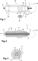
- reference 2 shows a post-discharge plasma coating device according to the present invention.
- the post-discharge plasma coating device 2 has a tubular shape and comprises an inner tubular wall 3 configured to receive a wired substrate 4 to be coated.
- the wired substrate 4 can move axially through the inner tubular wall 3 in a working direction 30 in order to be coated in a coating area 16 represented here in dotted lines.
- the coating area 16 is adjacent to the inner tubular wall 3 and is such that a plasma excited gas 19 can contact directly the substrate 4.
- the plasma excited gas 19 i.e.
- plasma gas that passes through the plasma zone of the device and that has been activated by energetic species from the plasma) flows axially in the working direction 30 and reacts with a precursor 8 in the coating area 16.
- the precursor 8 is preferably in the form of a precursor gas flow.
- the coating occurs in the coating area 16 where the substrate 4, the plasma excited gas 19 and the precursor 8 mix.
- the inner tubular wall 3 is designed to separate the plasma excited gas 19 and the precursor gas flow 8, as well as to protect the substrate 4 from direct plasma interaction.
- the inner tubular wall 3 is made of non-porous material.
- the inner tubular wall 3 is directly surrounded by an inner tubular electrode 6, made of conductive material as shown in figures 2 and 3 .
- the inner tubular wall 3 can form the inner electrode 6.
- the inner tubular wall 3 could be made of electrical conductive material or a combination of electrical conductive material and dielectric material.
- the inner tubular electrode 6 is surrounded by a coaxial outer tubular electrode 10.
- the two electrodes 6 and 10 are configured to be supplied with an electrical power source in order to produce a plasma when a plasma gas 12 is supplied between them, said plasma gas being thereby excited.
- the inner tubular electrode 6 extends axially towards the coating area 16 at least until, preferably beyond, an end of the outer electrode 10. Said end of the outer electrode is in the working direction 30.
- the plasma excited gas 19 appears at the end of the outer electrode 10, in the working direction 30.
- the coating area 16 corresponds to an area where the plasma excited gas 19, the substrate 4 and the precursor 8 mix.
- the inner tubular wall 3 is movable axially relative to the rest of the device 2 so as to axially displace the coating area 16.
- the device further comprises at least one dielectric tubular wall 14 extending axially between the two electrodes 6 and 10.
- This electrode composition so called dielectric barrier (DBD) discharges avoids the formation of electric arcs and allows the production of a homogenous low energy density plasma.
- a dielectric tubular wall 14 extends axially between the two electrodes 6 and 10 and supports the outer electrode 10.
- the outer electrode 10 extends axially along a portion of the dielectric tubular wall 14, preferably at least 10% and up to 100% of the length of said dielectric tubular wall.
- a second dielectric tubular wall (not represented), on and around the inner tubular electrode 6 can be used to form a DBD discharge with a symmetric configuration with two dielectrics.
- the dielectric tubular walls are made of a dielectric material including but not limited to material taken from the following list: quartz, alumina, silicon dioxide, glass, and any combination thereof.
- An annular space 15 or passage (represented in figure 3 ) is provided between the inner tubular electrode 6 and the dielectric tubular wall 14 supporting the outer tubular electrode 10, in order to receive the gas to be ionised.
- the annular space 15 can have approximately a width of 0.5 to 5 mm.
- the device 2 also comprises a connector 20 configured for supplying the annular space 15 with the plasma gas 12 for producing the plasma.
- the connector 20 (represented in figure 1 ) is axially located opposite to the coating area 16.
- the annular space can be between the dielectric tubular supporting the outer electrode, said dielectric tubular wall being a first dielectric tubular wall, and the second dielectric tubular wall.
- the device 2 further comprises an electrical power source 18 (represented in figure 1 ) configured for supplying a pulsed or alternating high voltage in order to ionize the plasma gas 12 flowing through the annular space 15.
- the electrical power source 18 is further configured so that the inner electrode 6 is electrically grounded and the outer electrode 10 is electrically supplied with the high voltage.
- the high voltage of the electrical power source 18 is preferably comprised between 1 and 50kV, more preferably between 1 and 15kV and/or the current supplied by the power source to the electrode 10 is less than 1000 mA.
- the frequency of the power source is comprised between 1 kHz and 100kHz. In general, the power source 18 will produce a high voltage with a low frequency in order to create the plasma.
- the plasma when a high voltage is applied to the outer electrode 10, the plasma is created by the phenomenon known as dielectric barrier discharge. A plasma is thus created in between the inner tubular electrode 6 and the dielectric tubular wall 14 supporting the outer electrode.
- the plasma excited gas 19 will flow axially towards the coating area 16 where said plasma excited gas 19 chemically reacts with the precursor 8 and the substrate 4.
- the precursor 8 is injected coaxially with the substrate 4 in the inner tubular wall 3.
- the precursor is preferably an organic chemical precursor possibly comprising non-organic groups (composed of atoms including but not limited to the list below: Si, Ti, Zr, Zn, Co, Fe, Pt, Pd, S, B, Cl, P, Mg, Ca, Au, Ag), with grow functional interfaces, which allows a good adhesion to the surface of the substrate and exhibits chemical groups of interest.
- the precursor 8 can be injected in the inner tubular wall 3 in a liquid or gaseous phase, preferably with a carrier gas.
- the precursor is preferably composed of C and H and may include functional groups, such as alcohol, alkane, allyl, amide, amine, carboxylic, epoxyde, etc and/or unsaturations...
- the precursor can be for example hexamethyldisiloxane, methyl methacrylate, titanium tetraisopropoxyde, aminopropyltriethoxysilane, said compounds carried in gas comprising but not limited to argon, helium, nitrogen, oxygen, hydrogen, and any combination thereof.
- the precursor is injected in the inner tubular wall 3 at whatever flow speed, along with a carrier gas flow.
- the mixture composed of precursor 8 and carrier gas is injected at a gas speed inferior, equal or superior, preferably equal or superior to the gas speed of the plasma gas 12 and plasma excited gas 19.
- the substrate 4 can be previously dipped or sprayed or impregnated with the precursor before moving through the inner tubular wall 3.
- an external confinement tube (not represented) can be setup in the coating area 16 in order to confine in a limited volume the mixture of the plasma excited gas 19, the chemical precursor 8 and the substrate 4.
- the confinement tube is preferably at the end of the outer tubular wall 14.
- the post-discharge plasma coating device 2 can have for example a dielectric tubular wall 14 supporting the outer electrode made of glass with an inner diameter of 10 mm.
- the outer tubular electrode 10 can have a length of 100 mm and the inner tubular wall 3 can have an outer diameter of 6 mm.
- the thickness of the inner tubular electrode 6 and outer tubular electrode 10 is comprised between 1 and 1000 ⁇ m, typically 100-300 ⁇ m.
- the annular space 15 between the dielectric tubular wall 14 supporting the outer electrode and the inner tubular electrode can be of 2 mm, said annular space corresponds to the space between the external diameter of the inner tubular electrode and the internal diameter of the dielectric tubular wall supporting the outer electrode.
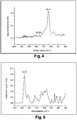
- a first coating with a monomer of HMDSO (Hexamethyldisiloxane) was performed on a wired substrate made of stainless steel. Nitrogen was used as the plasma gas with a flow speed of 50 l/s.
- the metallic wire was moved in the device at a speed of 100 cm/min and the HMDSO monomer was injected in the device with a vector gas or carrier gas at a flow speed of 10 l/min.
- the power supplied by the power source is of 80 W and the frequency of the signal is of 60 kHz.
- a "SiO 2 like" coating with very weak "Si-CH3" absorption bands was observed on the substrate with a Bruker Vertex 70 FTIR spectrometer and the results are represented in figure 4 .
Landscapes
- Chemical & Material Sciences (AREA)
- Engineering & Computer Science (AREA)
- Physics & Mathematics (AREA)
- Plasma & Fusion (AREA)
- Analytical Chemistry (AREA)
- Chemical Kinetics & Catalysis (AREA)
- General Chemical & Material Sciences (AREA)
- Materials Engineering (AREA)
- Mechanical Engineering (AREA)
- Metallurgy (AREA)
- Organic Chemistry (AREA)
- Spectroscopy & Molecular Physics (AREA)
- Fluid Mechanics (AREA)
- Chemical Vapour Deposition (AREA)
- Plasma Technology (AREA)
Claims (15)
- Nachentladungs-Plasmabeschichtungsvorrichtung (2) für ein drahtförmiges Substrat (4), die Folgendes umfasst:- eine innere röhrenförmige Elektrode (6) an einer inneren röhrenförmigen Wand (3) zur Aufnahme des Substrats (4) und eines Ausgangsstoffs (8), der sich axial in einer Arbeitsrichtung (30) bewegt;- eine äußere röhrenförmige Elektrode (10), die koaxial zu der inneren Elektrode (6) ist und diese umgibt;
wobei die innere und die äußere Elektroden (6; 10) so ausgelegt sind, dass sie mit einer elektrischen Stromquelle versorgt werden zur Erzeugung eines Plasmas, wenn ein Plasmagas (12) zwischen den Elektroden zugeführt und dadurch angeregt wird, wobei das plasmaangeregte Gas (19) axial in Arbeitsrichtung (30) strömt und mit dem Ausgangsstoff (8) in einem Beschichtungsbereich (16) am Ende der inneren röhrenförmigen Wand (3) in besagter Richtung (30) reagiert; dadurch gekennzeichnet, dass
sich die innere röhrenförmige Elektrode (6) axial in Richtung auf den Beschichtungsbereich (16) mindestens bis zum Ende der äußeren Elektrode (10), vorzugsweise über dieses hinaus, in Arbeitsrichtung (30) erstreckt und dass sich mindestens eine dielektrische röhrenförmige Wand (14) axial zwischen der inneren Elektrode (6) und der äußeren Elektrode (10) erstreckt. - Nachentladungs-Plasmabeschichtungsvorrichtung (2) nach Anspruch 1, wobei der Beschichtungsbereich (16) so beschaffen ist, dass das durch das Plasma angeregte Gas (19) direkt mit dem Substrat (4) in Kontakt kommen kann.
- Nachentladungs-Plasmabeschichtungsvorrichtung (2) nach einem der Ansprüche 1 und 2, wobei der Beschichtungsbereich (16) direkt an die innere röhrenförmige Wand (3) angrenzt.
- Nachentladungs-Plasmabeschichtungsvorrichtung (2) nach einem der Ansprüche 1 bis 3, wobei sich die mindestens eine dielektrische röhrenförmige Wand axial über die äußere Elektrode (10) in Arbeitsrichtung (30) hinaus erstreckt.
- Nachentladungs-Plasmabeschichtungsvorrichtung (2) nach einem der Ansprüche 1 bis 4, wobei die innere röhrenförmige Elektrode (6) die innere röhrenförmige Wand (3) umgibt oder durch die innere röhrenförmige Wand (3) gebildet wird.
- Nachentladungs-Plasmabeschichtungsvorrichtung (2) nach einem der Ansprüche 1 bis 5, wobei sich die innere röhrenförmige Elektrode (6) axial entlang eines Teils der inneren röhrenförmigen Wand (3) erstreckt, wobei dieser Teil bis zu 100 % beträgt.
- Nachentladungs-Plasmabeschichtungsvorrichtung (2) nach einem der Ansprüche 1 bis 6, wobei die dielektrische röhrenförmige Wand (14) oder eine der mindestens einen dielektrischen röhrenförmigen Wand (14) die äußere Elektrode (10) trägt.
- Nachentladungs-Plasmabeschichtungsvorrichtung (2) nach Anspruch 7, wobei sich die äußere Elektrode (10) axial entlang eines Teils der dielektrischen röhrenförmigen Wand (14) erstreckt, wobei dieser Teil vorzugsweise mindestens 10 % und bis zu 100 % beträgt.
- Nachentladungs-Plasmabeschichtungsvorrichtung (2) nach einem der Ansprüche 7 und 8, wobei die dielektrische röhrenförmige Wand (14), die die äußere Elektrode trägt, eine erste dielektrische röhrenförmige Wand ist, wobei die Vorrichtung eine zweite dielektrische röhrenförmige Wand umfasst, die sich zwischen der inneren röhrenförmigen Elektrode (6) und der ersten dielektrischen röhrenförmigen Wand (14) erstreckt.
- Nachentladungs-Plasmabeschichtungsvorrichtung (2) nach den Ansprüchen 7 und 9, bei der ein ringförmiger Raum (15) zwischen der dielektrischen röhrenförmigen Wand (14), die die äußere Elektrode (10) und die innere röhrenförmige Elektrode (6) oder zwischen der ersten und der zweiten dielektrischen röhrenförmigen Wand trägt, vorgesehen ist, wobei die Vorrichtung einen Verbinder (20) umfasst, der so konfiguriert ist, dass er den Raum mit dem Plasmagas (12) zur Erzeugung des Plasmas versorgt, wobei der Verbinder axial gegenüber dem Beschichtungsbereich (16) angeordnet ist.
- Nachentladungs-Plasmabeschichtungsvorrichtung (2) nach einem der Ansprüche 1 bis 10, wobei die innere röhrenförmige Wand (3) relativ zum Rest der Vorrichtung axial beweglich ist, um den Beschichtungsbereich (16) axial zu verschieben, und/oder wobei die Nachentladungs-Plasmabeschichtungsvorrichtung (2) ferner ein Begrenzungsrohr umfasst, das den Beschichtungsbereich (16) umgibt.
- Nachentladungs-Plasmabeschichtungsvorrichtung (2) nach einem der Ansprüche 1 bis 11, die ferner die elektrische Stromquelle (18) umfasst, die zum Zuführen einer gepulsten oder Wechsel-Hochspannung konfiguriert ist, wobei die Vorrichtung so konfiguriert ist, dass die innere Elektrode (6) elektrisch geerdet und die äußere Elektrode (10) elektrisch mit der Hochspannung versorgt wird.
- Nachentladungs-Plasmabeschichtungsvorrichtung (2) nach Anspruch 12, wobei die Hochspannung der elektrischen Stromquelle (18) zwischen 1 und 50 kV liegt und/oder der von dieser Quelle an die Elektrode (10) gelieferte Strom weniger als 1000 mA beträgt.
- Verfahren zum kontinuierlichen Beschichten eines drahtförmigen Substrats (4) mit einer Nachentladungs-Plasmabeschichtungsvorrichtung (2) mit einer inneren röhrenförmigen Elektrode (6) und einer äußeren röhrenförmigen Elektrode (10), wobei das Verfahren das Bewegen des Substrats (4) und eines Ausgangsstoffs (8) in einer Arbeitsrichtung (30) durch die innere röhrenförmige Elektrode (6) umfasst, während die äußeren und inneren Elektroden (10; 6) mit einer Hochspannung versorgt werden und Zuführen eines Plasmagases (12) zwischen die Elektroden, um ein durch Plasma angeregtes Gas (19) zu erzeugen, das axial zu einem Beschichtungsbereich (16) strömt, wo das durch Plasma angeregt Gas (19) chemisch mit dem Ausgangsstoff (8) auf dem Substrat (4) reagiert;
dadurch gekennzeichnet, dass die Nachentladungs-Plasmabeschichtungsvorrichtung einem der Ansprüche 1 bis 13 entspricht. - Verfahren nach Anspruch 14, bei dem der Ausgangsstoff (8) in einer flüssigen oder in einer gasförmigen Phase mit einem Trägergas injiziert wird und die Mischung aus dem Ausgangsstoff (8) und dem Trägergas durch die innere rohrförmige Wand (3) mit einer Gasgeschwindigkeit bewegt wird, die geringer, gleich oder höher, vorzugsweise gleich oder höher als die Gasgeschwindigkeit des Plasmagases (12) und des durch Plasma angeregten Gases (19) ist, oder bei dem das Substrat (4) eingetaucht oder besprüht oder mit dem Ausgangsstoff (8) getränkt wird, bevor es durch die innere Elektrode (6) bewegt wird.
Priority Applications (1)
| Application Number | Priority Date | Filing Date | Title |
|---|---|---|---|
| PL17762144T PL3513422T3 (pl) | 2016-09-15 | 2017-09-08 | Urządzenie do powlekania podłoży z drutu za pomocą plazmy po wyładowaniu |
Applications Claiming Priority (2)
| Application Number | Priority Date | Filing Date | Title |
|---|---|---|---|
| LU93222A LU93222B1 (en) | 2016-09-15 | 2016-09-15 | Post-discharge plasma coating device for wired substrates |
| PCT/EP2017/072635 WO2018050562A1 (en) | 2016-09-15 | 2017-09-08 | Post-discharge plasma coating device for wired substrates |
Publications (2)
| Publication Number | Publication Date |
|---|---|
| EP3513422A1 EP3513422A1 (de) | 2019-07-24 |
| EP3513422B1 true EP3513422B1 (de) | 2020-04-29 |
Family
ID=57178454
Family Applications (1)
| Application Number | Title | Priority Date | Filing Date |
|---|---|---|---|
| EP17762144.8A Active EP3513422B1 (de) | 2016-09-15 | 2017-09-08 | Nachentladungsplasmabeschichtungsvorrichtung für drahtgebundene substrate |
Country Status (7)
| Country | Link |
|---|---|
| US (1) | US11756770B2 (de) |
| EP (1) | EP3513422B1 (de) |
| JP (1) | JP7075666B2 (de) |
| ES (1) | ES2808116T3 (de) |
| LU (1) | LU93222B1 (de) |
| PL (1) | PL3513422T3 (de) |
| WO (1) | WO2018050562A1 (de) |
Families Citing this family (1)
| Publication number | Priority date | Publication date | Assignee | Title |
|---|---|---|---|---|
| JP7510037B2 (ja) * | 2019-08-06 | 2024-07-03 | ザ ロイヤル インスティテューション フォー ザ アドバンスメント オブ ラーニング/マクギル ユニバーシティ | 変換可能なプラズマ源および方法 |
Family Cites Families (9)
| Publication number | Priority date | Publication date | Assignee | Title |
|---|---|---|---|---|
| US7737382B2 (en) * | 2004-04-01 | 2010-06-15 | Lincoln Global, Inc. | Device for processing welding wire |
| KR20060098740A (ko) * | 2005-03-07 | 2006-09-19 | 삼성전자주식회사 | 플라즈마 장치와 그를 이용한 광섬유 모재 제작 장치 |
| JP4862193B2 (ja) * | 2006-07-24 | 2012-01-25 | 古河電気工業株式会社 | 半導体膜形成装置、半導体膜形成方法、及び半導体膜付き線条体 |
| CA2659298C (en) * | 2006-07-31 | 2012-03-06 | Tekna Plasma Systems Inc. | Plasma surface treatment using dielectric barrier discharges |
| US9288886B2 (en) * | 2008-05-30 | 2016-03-15 | Colorado State University Research Foundation | Plasma-based chemical source device and method of use thereof |
| US8994270B2 (en) * | 2008-05-30 | 2015-03-31 | Colorado State University Research Foundation | System and methods for plasma application |
| TWI432228B (zh) * | 2010-09-07 | 2014-04-01 | Univ Nat Cheng Kung | 微電漿產生裝置及其滅菌系統 |
| DE102012104224A1 (de) * | 2012-05-15 | 2013-11-21 | Plasmatreat Gmbh | Vorrichtung und Verfahren zur Behandlung eines Drahts aus leitfähigem Material |
| WO2014191012A1 (de) | 2013-05-27 | 2014-12-04 | Plasmatreat Gmbh | Vorrichtung und verfahren zur behandlung eines drahts aus leitfähigem material |
-
2016
- 2016-09-15 LU LU93222A patent/LU93222B1/en active IP Right Grant
-
2017
- 2017-09-08 EP EP17762144.8A patent/EP3513422B1/de active Active
- 2017-09-08 WO PCT/EP2017/072635 patent/WO2018050562A1/en not_active Ceased
- 2017-09-08 US US16/333,827 patent/US11756770B2/en active Active
- 2017-09-08 ES ES17762144T patent/ES2808116T3/es active Active
- 2017-09-08 PL PL17762144T patent/PL3513422T3/pl unknown
- 2017-09-08 JP JP2019512615A patent/JP7075666B2/ja active Active
Non-Patent Citations (1)
| Title |
|---|
| None * |
Also Published As
| Publication number | Publication date |
|---|---|
| US20190259577A1 (en) | 2019-08-22 |
| LU93222B1 (en) | 2018-04-11 |
| ES2808116T3 (es) | 2021-02-25 |
| EP3513422A1 (de) | 2019-07-24 |
| JP2019529700A (ja) | 2019-10-17 |
| US11756770B2 (en) | 2023-09-12 |
| JP7075666B2 (ja) | 2022-05-26 |
| PL3513422T3 (pl) | 2021-02-08 |
| WO2018050562A1 (en) | 2018-03-22 |
Similar Documents
| Publication | Publication Date | Title |
|---|---|---|
| US6800336B1 (en) | Method and device for plasma coating surfaces | |
| AU2014349815B2 (en) | Method for generating an atmospheric plasma jet and atmospheric plasma minitorch device | |
| US20230160067A1 (en) | Atmospheric cold plasma jet coating and surface treatment | |
| RU2462534C2 (ru) | Плазменная обработка поверхности с использованием диэлектрических барьерных разрядов | |
| CN101522941B (zh) | 在中空主体的内壁上进行等离子辅助化学气相沉积的方法与装置 | |
| EP2702840A1 (de) | Plasmabehandlung von substraten | |
| CN102112657B (zh) | 基板上沉积膜的工艺和装置 | |
| KR20170072882A (ko) | 부품, 밴드형 물질, 또는 도구의 표면에 코팅을 형성하는 장치 | |
| JP2002542586A (ja) | 大域大気圧プラズマジェット | |
| JPWO2007105428A1 (ja) | プラズマ発生装置用ノズル、プラズマ発生装置、プラズマ表面処理装置、プラズマ発生方法およびプラズマ表面処理方法 | |
| KR20130041810A (ko) | 기판의 플라즈마 처리 | |
| EP3513422B1 (de) | Nachentladungsplasmabeschichtungsvorrichtung für drahtgebundene substrate | |
| EP2300633B1 (de) | Verfahren und anlage zur gleichzeitigen ablagerung von filmen auf beiden seiten eines substrats | |
| US6007637A (en) | Process and apparatus for the dry treatment of metal surfaces | |
| JP5956302B2 (ja) | プラズマ処理装置、ヘテロ膜の形成方法 | |
| WO2021193651A1 (ja) | 大気圧リモートプラズマcvd装置、被膜形成方法、及びプラスチックボトルの製造方法 | |
| KR20060082400A (ko) | 플라즈마 발생 시스템 | |
| KR100947915B1 (ko) | Rf를 이용한 저파워, 고밀도 플라즈마 발생장치 | |
| US20190082525A1 (en) | Device For Forming Metal Components |
Legal Events
| Date | Code | Title | Description |
|---|---|---|---|
| STAA | Information on the status of an ep patent application or granted ep patent |
Free format text: STATUS: UNKNOWN |
|
| STAA | Information on the status of an ep patent application or granted ep patent |
Free format text: STATUS: THE INTERNATIONAL PUBLICATION HAS BEEN MADE |
|
| PUAI | Public reference made under article 153(3) epc to a published international application that has entered the european phase |
Free format text: ORIGINAL CODE: 0009012 |
|
| STAA | Information on the status of an ep patent application or granted ep patent |
Free format text: STATUS: REQUEST FOR EXAMINATION WAS MADE |
|
| 17P | Request for examination filed |
Effective date: 20190318 |
|
| AK | Designated contracting states |
Kind code of ref document: A1 Designated state(s): AL AT BE BG CH CY CZ DE DK EE ES FI FR GB GR HR HU IE IS IT LI LT LU LV MC MK MT NL NO PL PT RO RS SE SI SK SM TR |
|
| AX | Request for extension of the european patent |
Extension state: BA ME |
|
| GRAP | Despatch of communication of intention to grant a patent |
Free format text: ORIGINAL CODE: EPIDOSNIGR1 |
|
| STAA | Information on the status of an ep patent application or granted ep patent |
Free format text: STATUS: GRANT OF PATENT IS INTENDED |
|
| INTG | Intention to grant announced |
Effective date: 20191112 |
|
| DAV | Request for validation of the european patent (deleted) | ||
| DAX | Request for extension of the european patent (deleted) | ||
| GRAS | Grant fee paid |
Free format text: ORIGINAL CODE: EPIDOSNIGR3 |
|
| GRAA | (expected) grant |
Free format text: ORIGINAL CODE: 0009210 |
|
| STAA | Information on the status of an ep patent application or granted ep patent |
Free format text: STATUS: THE PATENT HAS BEEN GRANTED |
|
| AK | Designated contracting states |
Kind code of ref document: B1 Designated state(s): AL AT BE BG CH CY CZ DE DK EE ES FI FR GB GR HR HU IE IS IT LI LT LU LV MC MK MT NL NO PL PT RO RS SE SI SK SM TR |
|
| REG | Reference to a national code |
Ref country code: GB Ref legal event code: FG4D |
|
| REG | Reference to a national code |
Ref country code: CH Ref legal event code: EP |
|
| REG | Reference to a national code |
Ref country code: DE Ref legal event code: R096 Ref document number: 602017015813 Country of ref document: DE |
|
| REG | Reference to a national code |
Ref country code: AT Ref legal event code: REF Ref document number: 1264550 Country of ref document: AT Kind code of ref document: T Effective date: 20200515 |
|
| REG | Reference to a national code |
Ref country code: IE Ref legal event code: FG4D |
|
| REG | Reference to a national code |
Ref country code: CH Ref legal event code: NV Representative=s name: DR. ALEXANDER MILLER, LL.M. RECHTSANWALT (D), CH |
|
| REG | Reference to a national code |
Ref country code: FI Ref legal event code: FGE |
|
| REG | Reference to a national code |
Ref country code: NL Ref legal event code: FP |
|
| REG | Reference to a national code |
Ref country code: SE Ref legal event code: TRGR |
|
| REG | Reference to a national code |
Ref country code: NO Ref legal event code: T2 Effective date: 20200429 |
|
| REG | Reference to a national code |
Ref country code: LT Ref legal event code: MG4D |
|
| PG25 | Lapsed in a contracting state [announced via postgrant information from national office to epo] |
Ref country code: IS Free format text: LAPSE BECAUSE OF FAILURE TO SUBMIT A TRANSLATION OF THE DESCRIPTION OR TO PAY THE FEE WITHIN THE PRESCRIBED TIME-LIMIT Effective date: 20200829 Ref country code: PT Free format text: LAPSE BECAUSE OF FAILURE TO SUBMIT A TRANSLATION OF THE DESCRIPTION OR TO PAY THE FEE WITHIN THE PRESCRIBED TIME-LIMIT Effective date: 20200831 Ref country code: LT Free format text: LAPSE BECAUSE OF FAILURE TO SUBMIT A TRANSLATION OF THE DESCRIPTION OR TO PAY THE FEE WITHIN THE PRESCRIBED TIME-LIMIT Effective date: 20200429 Ref country code: GR Free format text: LAPSE BECAUSE OF FAILURE TO SUBMIT A TRANSLATION OF THE DESCRIPTION OR TO PAY THE FEE WITHIN THE PRESCRIBED TIME-LIMIT Effective date: 20200730 |
|
| REG | Reference to a national code |
Ref country code: SK Ref legal event code: T3 Ref document number: E 34869 Country of ref document: SK |
|
| PG25 | Lapsed in a contracting state [announced via postgrant information from national office to epo] |
Ref country code: BG Free format text: LAPSE BECAUSE OF FAILURE TO SUBMIT A TRANSLATION OF THE DESCRIPTION OR TO PAY THE FEE WITHIN THE PRESCRIBED TIME-LIMIT Effective date: 20200729 Ref country code: HR Free format text: LAPSE BECAUSE OF FAILURE TO SUBMIT A TRANSLATION OF THE DESCRIPTION OR TO PAY THE FEE WITHIN THE PRESCRIBED TIME-LIMIT Effective date: 20200429 Ref country code: LV Free format text: LAPSE BECAUSE OF FAILURE TO SUBMIT A TRANSLATION OF THE DESCRIPTION OR TO PAY THE FEE WITHIN THE PRESCRIBED TIME-LIMIT Effective date: 20200429 Ref country code: RS Free format text: LAPSE BECAUSE OF FAILURE TO SUBMIT A TRANSLATION OF THE DESCRIPTION OR TO PAY THE FEE WITHIN THE PRESCRIBED TIME-LIMIT Effective date: 20200429 |
|
| PG25 | Lapsed in a contracting state [announced via postgrant information from national office to epo] |
Ref country code: AL Free format text: LAPSE BECAUSE OF FAILURE TO SUBMIT A TRANSLATION OF THE DESCRIPTION OR TO PAY THE FEE WITHIN THE PRESCRIBED TIME-LIMIT Effective date: 20200429 |
|
| PG25 | Lapsed in a contracting state [announced via postgrant information from national office to epo] |
Ref country code: DK Free format text: LAPSE BECAUSE OF FAILURE TO SUBMIT A TRANSLATION OF THE DESCRIPTION OR TO PAY THE FEE WITHIN THE PRESCRIBED TIME-LIMIT Effective date: 20200429 Ref country code: SM Free format text: LAPSE BECAUSE OF FAILURE TO SUBMIT A TRANSLATION OF THE DESCRIPTION OR TO PAY THE FEE WITHIN THE PRESCRIBED TIME-LIMIT Effective date: 20200429 Ref country code: EE Free format text: LAPSE BECAUSE OF FAILURE TO SUBMIT A TRANSLATION OF THE DESCRIPTION OR TO PAY THE FEE WITHIN THE PRESCRIBED TIME-LIMIT Effective date: 20200429 Ref country code: RO Free format text: LAPSE BECAUSE OF FAILURE TO SUBMIT A TRANSLATION OF THE DESCRIPTION OR TO PAY THE FEE WITHIN THE PRESCRIBED TIME-LIMIT Effective date: 20200429 |
|
| REG | Reference to a national code |
Ref country code: DE Ref legal event code: R097 Ref document number: 602017015813 Country of ref document: DE |
|
| REG | Reference to a national code |
Ref country code: ES Ref legal event code: FG2A Ref document number: 2808116 Country of ref document: ES Kind code of ref document: T3 Effective date: 20210225 |
|
| PLBE | No opposition filed within time limit |
Free format text: ORIGINAL CODE: 0009261 |
|
| STAA | Information on the status of an ep patent application or granted ep patent |
Free format text: STATUS: NO OPPOSITION FILED WITHIN TIME LIMIT |
|
| 26N | No opposition filed |
Effective date: 20210201 |
|
| PG25 | Lapsed in a contracting state [announced via postgrant information from national office to epo] |
Ref country code: SI Free format text: LAPSE BECAUSE OF FAILURE TO SUBMIT A TRANSLATION OF THE DESCRIPTION OR TO PAY THE FEE WITHIN THE PRESCRIBED TIME-LIMIT Effective date: 20200429 |
|
| PG25 | Lapsed in a contracting state [announced via postgrant information from national office to epo] |
Ref country code: IE Free format text: LAPSE BECAUSE OF NON-PAYMENT OF DUE FEES Effective date: 20200908 |
|
| GBPC | Gb: european patent ceased through non-payment of renewal fee |
Effective date: 20210908 |
|
| PG25 | Lapsed in a contracting state [announced via postgrant information from national office to epo] |
Ref country code: TR Free format text: LAPSE BECAUSE OF FAILURE TO SUBMIT A TRANSLATION OF THE DESCRIPTION OR TO PAY THE FEE WITHIN THE PRESCRIBED TIME-LIMIT Effective date: 20200429 Ref country code: MT Free format text: LAPSE BECAUSE OF FAILURE TO SUBMIT A TRANSLATION OF THE DESCRIPTION OR TO PAY THE FEE WITHIN THE PRESCRIBED TIME-LIMIT Effective date: 20200429 Ref country code: CY Free format text: LAPSE BECAUSE OF FAILURE TO SUBMIT A TRANSLATION OF THE DESCRIPTION OR TO PAY THE FEE WITHIN THE PRESCRIBED TIME-LIMIT Effective date: 20200429 |
|
| PG25 | Lapsed in a contracting state [announced via postgrant information from national office to epo] |
Ref country code: MK Free format text: LAPSE BECAUSE OF FAILURE TO SUBMIT A TRANSLATION OF THE DESCRIPTION OR TO PAY THE FEE WITHIN THE PRESCRIBED TIME-LIMIT Effective date: 20200429 Ref country code: MC Free format text: LAPSE BECAUSE OF FAILURE TO SUBMIT A TRANSLATION OF THE DESCRIPTION OR TO PAY THE FEE WITHIN THE PRESCRIBED TIME-LIMIT Effective date: 20200429 |
|
| PG25 | Lapsed in a contracting state [announced via postgrant information from national office to epo] |
Ref country code: GB Free format text: LAPSE BECAUSE OF NON-PAYMENT OF DUE FEES Effective date: 20210908 |
|
| PGFP | Annual fee paid to national office [announced via postgrant information from national office to epo] |
Ref country code: LU Payment date: 20230830 Year of fee payment: 7 |
|
| PGFP | Annual fee paid to national office [announced via postgrant information from national office to epo] |
Ref country code: IT Payment date: 20230925 Year of fee payment: 7 Ref country code: FI Payment date: 20230925 Year of fee payment: 7 Ref country code: CZ Payment date: 20230904 Year of fee payment: 7 Ref country code: AT Payment date: 20230925 Year of fee payment: 7 Ref country code: NO Payment date: 20230830 Year of fee payment: 7 |
|
| PGFP | Annual fee paid to national office [announced via postgrant information from national office to epo] |
Ref country code: SK Payment date: 20230831 Year of fee payment: 7 Ref country code: SE Payment date: 20230830 Year of fee payment: 7 Ref country code: PL Payment date: 20230818 Year of fee payment: 7 Ref country code: NL Payment date: 20230925 Year of fee payment: 7 Ref country code: FR Payment date: 20230928 Year of fee payment: 7 Ref country code: BE Payment date: 20230928 Year of fee payment: 7 |
|
| PGFP | Annual fee paid to national office [announced via postgrant information from national office to epo] |
Ref country code: ES Payment date: 20231004 Year of fee payment: 7 |
|
| PGFP | Annual fee paid to national office [announced via postgrant information from national office to epo] |
Ref country code: DE Payment date: 20230928 Year of fee payment: 7 Ref country code: CH Payment date: 20231001 Year of fee payment: 7 |
|
| REG | Reference to a national code |
Ref country code: DE Ref legal event code: R119 Ref document number: 602017015813 Country of ref document: DE |
|
| PG25 | Lapsed in a contracting state [announced via postgrant information from national office to epo] |
Ref country code: FI Free format text: LAPSE BECAUSE OF NON-PAYMENT OF DUE FEES Effective date: 20240908 |
|
| REG | Reference to a national code |
Ref country code: SK Ref legal event code: MM4A Ref document number: E 34869 Country of ref document: SK Effective date: 20240908 |
|
| PG25 | Lapsed in a contracting state [announced via postgrant information from national office to epo] |
Ref country code: CZ Free format text: LAPSE BECAUSE OF NON-PAYMENT OF DUE FEES Effective date: 20240908 |
|
| REG | Reference to a national code |
Ref country code: SE Ref legal event code: EUG |
|
| REG | Reference to a national code |
Ref country code: CH Ref legal event code: PL |
|
| REG | Reference to a national code |
Ref country code: NL Ref legal event code: MM Effective date: 20241001 |
|
| REG | Reference to a national code |
Ref country code: AT Ref legal event code: MM01 Ref document number: 1264550 Country of ref document: AT Kind code of ref document: T Effective date: 20240908 |
|
| PG25 | Lapsed in a contracting state [announced via postgrant information from national office to epo] |
Ref country code: LU Free format text: LAPSE BECAUSE OF NON-PAYMENT OF DUE FEES Effective date: 20240908 |
|
| PG25 | Lapsed in a contracting state [announced via postgrant information from national office to epo] |
Ref country code: NL Free format text: LAPSE BECAUSE OF NON-PAYMENT OF DUE FEES Effective date: 20241001 |
|
| PG25 | Lapsed in a contracting state [announced via postgrant information from national office to epo] |
Ref country code: DE Free format text: LAPSE BECAUSE OF NON-PAYMENT OF DUE FEES Effective date: 20250401 |
|
| REG | Reference to a national code |
Ref country code: BE Ref legal event code: MM Effective date: 20240930 |
|
| PG25 | Lapsed in a contracting state [announced via postgrant information from national office to epo] |
Ref country code: NO Free format text: LAPSE BECAUSE OF NON-PAYMENT OF DUE FEES Effective date: 20240930 |
|
| PG25 | Lapsed in a contracting state [announced via postgrant information from national office to epo] |
Ref country code: IT Free format text: LAPSE BECAUSE OF NON-PAYMENT OF DUE FEES Effective date: 20240908 Ref country code: BE Free format text: LAPSE BECAUSE OF NON-PAYMENT OF DUE FEES Effective date: 20240930 |
|
| PG25 | Lapsed in a contracting state [announced via postgrant information from national office to epo] |
Ref country code: FR Free format text: LAPSE BECAUSE OF NON-PAYMENT OF DUE FEES Effective date: 20240930 |
|
| PG25 | Lapsed in a contracting state [announced via postgrant information from national office to epo] |
Ref country code: CH Free format text: LAPSE BECAUSE OF NON-PAYMENT OF DUE FEES Effective date: 20240930 |
|
| PG25 | Lapsed in a contracting state [announced via postgrant information from national office to epo] |
Ref country code: AT Free format text: LAPSE BECAUSE OF NON-PAYMENT OF DUE FEES Effective date: 20240908 |
|
| PG25 | Lapsed in a contracting state [announced via postgrant information from national office to epo] |
Ref country code: SK Free format text: LAPSE BECAUSE OF NON-PAYMENT OF DUE FEES Effective date: 20240908 |
|
| REG | Reference to a national code |
Ref country code: AT Ref legal event code: UEP Ref document number: 1264550 Country of ref document: AT Kind code of ref document: T Effective date: 20200429 |
|
| PG25 | Lapsed in a contracting state [announced via postgrant information from national office to epo] |
Ref country code: SE Free format text: LAPSE BECAUSE OF NON-PAYMENT OF DUE FEES Effective date: 20240909 |
|
| REG | Reference to a national code |
Ref country code: ES Ref legal event code: FD2A Effective date: 20251028 |
|
| PG25 | Lapsed in a contracting state [announced via postgrant information from national office to epo] |
Ref country code: ES Free format text: LAPSE BECAUSE OF NON-PAYMENT OF DUE FEES Effective date: 20240909 |