EP3512044A1 - Card edge connector system - Google Patents
Card edge connector system Download PDFInfo
- Publication number
- EP3512044A1 EP3512044A1 EP19150811.8A EP19150811A EP3512044A1 EP 3512044 A1 EP3512044 A1 EP 3512044A1 EP 19150811 A EP19150811 A EP 19150811A EP 3512044 A1 EP3512044 A1 EP 3512044A1
- Authority
- EP
- European Patent Office
- Prior art keywords
- mating
- card
- contact
- contacts
- edge connector
- Prior art date
- Legal status (The legal status is an assumption and is not a legal conclusion. Google has not performed a legal analysis and makes no representation as to the accuracy of the status listed.)
- Granted
Links
Images




Classifications
-
- H—ELECTRICITY
- H01—ELECTRIC ELEMENTS
- H01R—ELECTRICALLY-CONDUCTIVE CONNECTIONS; STRUCTURAL ASSOCIATIONS OF A PLURALITY OF MUTUALLY-INSULATED ELECTRICAL CONNECTING ELEMENTS; COUPLING DEVICES; CURRENT COLLECTORS
- H01R12/00—Structural associations of a plurality of mutually-insulated electrical connecting elements, specially adapted for printed circuits, e.g. printed circuit boards [PCB], flat or ribbon cables, or like generally planar structures, e.g. terminal strips, terminal blocks; Coupling devices specially adapted for printed circuits, flat or ribbon cables, or like generally planar structures; Terminals specially adapted for contact with, or insertion into, printed circuits, flat or ribbon cables, or like generally planar structures
- H01R12/70—Coupling devices
- H01R12/71—Coupling devices for rigid printing circuits or like structures
- H01R12/72—Coupling devices for rigid printing circuits or like structures coupling with the edge of the rigid printed circuits or like structures
- H01R12/721—Coupling devices for rigid printing circuits or like structures coupling with the edge of the rigid printed circuits or like structures cooperating directly with the edge of the rigid printed circuits
-
- H—ELECTRICITY
- H01—ELECTRIC ELEMENTS
- H01R—ELECTRICALLY-CONDUCTIVE CONNECTIONS; STRUCTURAL ASSOCIATIONS OF A PLURALITY OF MUTUALLY-INSULATED ELECTRICAL CONNECTING ELEMENTS; COUPLING DEVICES; CURRENT COLLECTORS
- H01R12/00—Structural associations of a plurality of mutually-insulated electrical connecting elements, specially adapted for printed circuits, e.g. printed circuit boards [PCB], flat or ribbon cables, or like generally planar structures, e.g. terminal strips, terminal blocks; Coupling devices specially adapted for printed circuits, flat or ribbon cables, or like generally planar structures; Terminals specially adapted for contact with, or insertion into, printed circuits, flat or ribbon cables, or like generally planar structures
- H01R12/70—Coupling devices
- H01R12/71—Coupling devices for rigid printing circuits or like structures
- H01R12/72—Coupling devices for rigid printing circuits or like structures coupling with the edge of the rigid printed circuits or like structures
- H01R12/73—Coupling devices for rigid printing circuits or like structures coupling with the edge of the rigid printed circuits or like structures connecting to other rigid printed circuits or like structures
-
- H—ELECTRICITY
- H01—ELECTRIC ELEMENTS
- H01R—ELECTRICALLY-CONDUCTIVE CONNECTIONS; STRUCTURAL ASSOCIATIONS OF A PLURALITY OF MUTUALLY-INSULATED ELECTRICAL CONNECTING ELEMENTS; COUPLING DEVICES; CURRENT COLLECTORS
- H01R13/00—Details of coupling devices of the kinds covered by groups H01R12/70 or H01R24/00 - H01R33/00
- H01R13/02—Contact members
-
- H—ELECTRICITY
- H01—ELECTRIC ELEMENTS
- H01R—ELECTRICALLY-CONDUCTIVE CONNECTIONS; STRUCTURAL ASSOCIATIONS OF A PLURALITY OF MUTUALLY-INSULATED ELECTRICAL CONNECTING ELEMENTS; COUPLING DEVICES; CURRENT COLLECTORS
- H01R13/00—Details of coupling devices of the kinds covered by groups H01R12/70 or H01R24/00 - H01R33/00
- H01R13/02—Contact members
- H01R13/10—Sockets for co-operation with pins or blades
- H01R13/11—Resilient sockets
-
- H—ELECTRICITY
- H01—ELECTRIC ELEMENTS
- H01R—ELECTRICALLY-CONDUCTIVE CONNECTIONS; STRUCTURAL ASSOCIATIONS OF A PLURALITY OF MUTUALLY-INSULATED ELECTRICAL CONNECTING ELEMENTS; COUPLING DEVICES; CURRENT COLLECTORS
- H01R13/00—Details of coupling devices of the kinds covered by groups H01R12/70 or H01R24/00 - H01R33/00
- H01R13/02—Contact members
- H01R13/22—Contacts for co-operating by abutting
- H01R13/24—Contacts for co-operating by abutting resilient; resiliently-mounted
- H01R13/2464—Contacts for co-operating by abutting resilient; resiliently-mounted characterized by the contact point
- H01R13/2492—Contacts for co-operating by abutting resilient; resiliently-mounted characterized by the contact point multiple contact points
-
- H—ELECTRICITY
- H01—ELECTRIC ELEMENTS
- H01R—ELECTRICALLY-CONDUCTIVE CONNECTIONS; STRUCTURAL ASSOCIATIONS OF A PLURALITY OF MUTUALLY-INSULATED ELECTRICAL CONNECTING ELEMENTS; COUPLING DEVICES; CURRENT COLLECTORS
- H01R13/00—Details of coupling devices of the kinds covered by groups H01R12/70 or H01R24/00 - H01R33/00
- H01R13/46—Bases; Cases
- H01R13/502—Bases; Cases composed of different pieces
-
- H—ELECTRICITY
- H01—ELECTRIC ELEMENTS
- H01R—ELECTRICALLY-CONDUCTIVE CONNECTIONS; STRUCTURAL ASSOCIATIONS OF A PLURALITY OF MUTUALLY-INSULATED ELECTRICAL CONNECTING ELEMENTS; COUPLING DEVICES; CURRENT COLLECTORS
- H01R13/00—Details of coupling devices of the kinds covered by groups H01R12/70 or H01R24/00 - H01R33/00
- H01R13/62—Means for facilitating engagement or disengagement of coupling parts or for holding them in engagement
- H01R13/621—Bolt, set screw or screw clamp
-
- H—ELECTRICITY
- H01—ELECTRIC ELEMENTS
- H01R—ELECTRICALLY-CONDUCTIVE CONNECTIONS; STRUCTURAL ASSOCIATIONS OF A PLURALITY OF MUTUALLY-INSULATED ELECTRICAL CONNECTING ELEMENTS; COUPLING DEVICES; CURRENT COLLECTORS
- H01R13/00—Details of coupling devices of the kinds covered by groups H01R12/70 or H01R24/00 - H01R33/00
- H01R13/62—Means for facilitating engagement or disengagement of coupling parts or for holding them in engagement
- H01R13/639—Additional means for holding or locking coupling parts together, after engagement, e.g. separate keylock, retainer strap
-
- H—ELECTRICITY
- H01—ELECTRIC ELEMENTS
- H01R—ELECTRICALLY-CONDUCTIVE CONNECTIONS; STRUCTURAL ASSOCIATIONS OF A PLURALITY OF MUTUALLY-INSULATED ELECTRICAL CONNECTING ELEMENTS; COUPLING DEVICES; CURRENT COLLECTORS
- H01R13/00—Details of coupling devices of the kinds covered by groups H01R12/70 or H01R24/00 - H01R33/00
- H01R13/46—Bases; Cases
- H01R13/533—Bases, cases made for use in extreme conditions, e.g. high temperature, radiation, vibration, corrosive environment, pressure
Definitions
- the subject matter herein relates generally to card edge connector systems.
- Card edge connector systems are known that include the circuit cards configured to be mated with the card edge connectors.
- known card edge connector systems fail to meet environmental and mechanical requirements for certain applications, such as military and aerospace applications, where the components are subjected to harsh environments. For example, some applications may subject the components to vibration during use. Vibration causes wear on the contacts and may lead to unintentional loss of contact. Additionally, the circuit card may cause damage to the card edge connector, such as the contacts of the card edge connector, when the circuit card moves relative to the card edge connector. As connector components are made smaller for certain applications, size constraints make electrical connection between the contacts and the circuit card difficult to achieve.
- a card edge connector including a housing having a mounting end configured to be mounted to a host circuit board and a mating end having a card slot configured to receive a circuit card.
- the housing has an upper wall above the card slot and a lower wall below the card slot.
- the upper wall has upper contact channels and the lower wall has lower contact channels.
- Upper contacts are received in the upper contact channels and lower contacts are received in the lower contact channels.
- the upper contacts include corresponding mounting ends and mating ends with the mounting ends extending from the housing for mounting to the host circuit board and the mating ends having a first mating interface and a second mating interface remote from the first mating interface.
- the first and second mating interfaces of the upper contacts define first and second points of contact with the same contact pad on an upper surface of the circuit card.
- the lower contacts include corresponding mounting ends and mating ends with the mounting ends extending from the housing for mounting to the host circuit board and the mating ends having a first mating interface and a second mating interface remote from the first mating interface.
- the first and second mating interfaces of the lower contacts define first and second points of contact with the same contact pad on a lower surface of the circuit card.
- a card edge connector including a housing having a mounting end configured to be mounted to a host circuit board and a mating end having a card slot configured to receive a circuit card.
- the housing has an upper wall above the card slot and a lower wall below the card slot.
- the upper wall has upper contact channels and the lower wall has lower contact channels.
- Upper contacts are received in the upper contact channels and lower contacts are received in the lower contact channels.
- the upper contacts include corresponding mounting ends and mating ends with the mounting ends extending from the housing for mounting to the host circuit board and the mating ends having a first mating interface and a second mating interface remote from the first mating interface.
- the first and second mating interfaces of the upper contacts define first and second points of contact with the same contact pad on an upper surface of the circuit card.
- the lower contacts include corresponding mounting ends and mating ends with the mounting ends extending from the housing for mounting to the host circuit board and the mating ends having a first mating interface and a second mating interface remote from the first mating interface.
- the first and second mating interfaces of the lower contacts define first and second points of contact with the same contact pad on a lower surface of the circuit card.
- a card edge connector system including a circuit card having a mating end including a mating edge between an upper surface and a lower surface and having upper contact pads on the upper surface and lower contact pads on the lower surface.
- the card edge connector system includes a card edge connector configured to be mounted to a host circuit board.
- the card edge connector includes a housing having a card slot receiving the circuit card. The housing holds upper contacts and lower contacts configured to be terminated to the host circuit board.
- the upper contacts have mating ends mated with corresponding upper contact pads having a first mating interface and a second mating interface remote from the first mating interface defining first and second points of contact with the same upper contact pad.
- the lower contacts have mating ends mated with corresponding lower contact pads having a first mating interface and a second mating interface remote from the first mating interface defining first and second points of contact with the same lower contact pad.
- the circuit card is received in the card slot of the housing in a loading direction angled non-parallel to the host circuit board to a loaded position.
- the circuit card is rotated in a mating direction within the card slot toward the host circuit board to a mated position.
- the circuit card is held in the card slot in the mated position with the circuit card extending from the housing parallel to the host circuit board.
- a card edge connector system in a further embodiment, includes a circuit card having a mating end including a mating edge between an upper surface and a lower surface having upper contact pads on the upper surface and lower contact pads on the lower surface and having a fastener opening extending therethrough.
- the card edge connector system includes a card edge connector configured to be mounted to a host circuit board.
- the card edge connector includes a housing having a card slot receiving the circuit card and having a fastener opening proximate to the card slot. The housing holds upper contacts and lower contacts configured to be terminated to the host circuit board.
- the upper contacts have mating ends mated with corresponding upper contact pads having a first mating interface and a second mating interface remote from the first mating interface defining first and second points of contact with the same upper contact pad.
- the lower contacts have mating ends mated with corresponding lower contact pads having a first mating interface and a second mating interface remote from the first mating interface defining first and second points of contact with the same lower contact pad.
- the circuit card is secured to the housing of the card edge connector using a fastener received in the fastener openings in the circuit card and the housing to fix the circuit card to the housing.
- FIG. 1 is a perspective view of a card edge connector system 100 in accordance with an exemplary embodiment.
- the card edge connector system 100 includes a card edge connector 102 mounted to a host circuit board 104.
- the card edge connector system 100 includes a circuit card 106 coupled to the card edge connector 102.
- the circuit card 106 is secured to the card edge connector 102 using a fastener 108.
- the fastener 108 retains the circuit card 106 in the card edge connector 102.
- the fastener 108 reduces relative movement between the circuit card 106 and the card edge connector 102, such as during vibration of the card edge connector system 100 making a robust electrical connection between the components and reducing wear on the components.
- the card edge connector 102 includes a housing 110 having a mounting end 112 mounted to the host circuit board 104 and a mating end 114 having a card slot 116 that receives the circuit card 106.
- the mounting end 112 is provided at a bottom 118 of the housing 110.
- the housing 110 includes a top 120 opposite the bottom 118.
- the mating end 114 is provided at a front 122 of the housing 110.
- the housing 110 includes a rear 124 opposite the front 122.
- the housing 110 extends between a first side 126 and a second side 128.
- the fastener 108 is approximately centered between the first and second sides 126, 128.
- the card edge connector system 100 may include a plurality of fasteners 108, such as proximate to the first and second sides 126, 128.
- FIG. 2 is a side view of the card edge connector system 100 in accordance with an exemplary embodiment.
- Figure 2 illustrates the circuit card 106 being loaded into the card edge connector 102.
- the circuit card 106 is loaded into the card edge connector 102 at an angle rather than be loaded straight into the card edge connector 102.
- the circuit card 106 is loaded into the card edge connector 102 in a loading direction 130 angled nonparallel to the host circuit board 104.
- the circuit card 106 is configured to be rotated in a mating direction 132 within the card slot 116 toward the host circuit board 104 to a mated position (shown in Figure 1 ). In the mated position, the circuit card 106 extends from the housing 110 generally parallel to the host circuit board. As such, the circuit card 106 is loaded into the housing 110 at an angle relative to the final mated position of the circuit card 106.
- the card edge connector system 100 may include standoffs 134 on the host circuit board 104.
- the standoffs 134 may support the circuit card 106 in the mated position.
- the stand offs 134 hold the circuit card 106 elevated above the host circuit board 104 such that a space is formed between the circuit card 106 and the host circuit board 104.
- Other components may occupy the space.
- electrical components mounted to the host circuit board 104 or the bottom side of the circuit card 106 may be positioned in the space between the circuit card 106 and the host circuit board 104. Loading of the circuit card 106 into the housing 110 at the angled loading direction 130 ensures that the components do not interfere with loading the circuit card 106 into the card edge connector 102.
- FIG. 3 is a perspective view of the card edge connector 102 in accordance with an exemplary embodiment.
- the card edge connector 102 includes a plurality of upper contacts 150 arranged in a row along the upper side of the card slot 116 and a plurality of lower contacts 152 arranged in a row along the lower side of the card slot 116.
- the upper contacts 150 are held in the housing 110 for mating with the circuit card 106 and the host circuit board 104.
- the lower contacts 152 are held in the housing 110 for mating with the circuit card 106 and the host circuit board 104.
- the upper contacts 150 are configured to be mounted to the housing 110 at the rear 124 and the lower contacts 152 are configured to be mounted to the housing 110 at the front 122. Other arrangements are possible in alternative embodiments.
- the card edge connector 102 includes mounting tabs 154 used for mounting the housing 110 to the host circuit board 104.
- the mounting tabs 154 may be received in the bottom 118 of the housing 110 proximate to the first and second sides 126, 128.
- the mounting tabs 154 may be held in the housing 110 by an interference fit.
- the mounting tabs 154 have mounting legs 156 configured to be mounted to the host circuit board 104.
- the mounting legs 156 may be solder legs configured to be soldered to the host circuit board 104.
- the mounting legs 156 may extend into the vias in the host circuit board 104 or may be surface mounted to the host circuit board 104.
- the housing 110 includes an upper wall 160 above the card slot 116 and a lower wall 162 below the card slot 116.
- the upper contacts 150 may extend along the upper wall 160 and the lower contacts 152 may extend along the lower wall 162.
- the upper wall 160 includes upper contact channels 164 (shown in Figure 8 ) that receive corresponding upper contacts 150.
- the lower wall 162 includes lower contact channels 166 that receive corresponding lower contacts 152.
- the housing 110 includes a mid-wall 170 between first and second side walls at the first and second sides 126, 128, respectively.
- the sidewalls 172, 174 are provided at opposite sides of the card slot 116.
- the mid-wall 170 divides the card slot 116 into card slot portions.
- a first set of upper and lower contacts 150, 152 may be provided between the mid-wall 170 and the first side wall 172 and a second set of upper and lower contacts 150, 152 may be provided between the mid-wall 170 and the second side wall 174.
- the mid-wall 170 is used to locate the circuit card 106 in the card slot 116.
- the circuit card 106 may engage one or more sides of the mid-wall 170 to locate the circuit card 106 in the card slot 116.
- the front edge of the mid-wall 170 may be chamfered to help guide loading of the circuit card 106 into the card slot 116.
- the housing 110 includes a fastener opening 176 that receive the fastener 108.
- the fastener opening 176 may be threaded.
- the fastener opening 176 may be aligned with the mid-wall 170.
- Other locations are possible in alternative embodiments, such as at the first side wall 172 and/or the second side wall 174.
- Figure 4 is a side view of a portion of the card edge connector 102 showing the upper contact 150 and the lower contact 152 with the housing 110 removed.
- a receiving space 200 is defined between the upper contact 150 and lower contact 152 for receiving the circuit card 106.
- the upper and lower contacts 150, 152 are stamped contacts stamped into the shapes illustrated in Figure 4 . By stamping the contacts into the predetermined shapes, the contacts may be manufactured in a repeatable manner, such as compared to contacts that are formed by bending into the predetermined shape.
- the upper contact 150 includes a mounting end 210 and a mating end 212 opposite the mounting end 210.
- the mounting end 210 is configured to be mounted to the host circuit board 104.
- the mating end 212 is configured to be mated with the circuit card 106.
- the upper contact 150 includes a base 214 between the mounting end 210 and the mating end 212. In the illustrated embodiment, the base 214 extends generally vertically; however, the base 214 may extend in other directions in alternative embodiments.
- the base 214 includes a mounting post 216 used to secure the upper contact 150 to the housing 110. In the illustrated embodiment, the mounting post 216 is forward facing.
- the mounting end 210 includes a solder tail 218 configured to be soldered to the host circuit board 104.
- the solder tail 218 extends horizontally from the base 214.
- the solder tail 218 is provided at the bottom of the upper contact 150.
- Other types of mounting ends 210 may be provided in alternative embodiments, such as a compliant pin configured to be press-fit into the host circuit board 104.
- the mating end 212 is cantilevered from the base 214 and extends forward of the base 214.
- the mating end 212 extends from the base 214 at a corner 220.
- the mating end 212 includes a support arm 222 and the spring arm 224 extending from the support arm 222.
- the support arm 222 is provided at the top of the upper contact 150.
- the spring arm 224 is folded under the support arm 222 at a front bend 226.
- the support arm 222 may extend generally horizontally and the spring arm 224 may extend generally horizontally below the support arm 222; however, the spring arm 224 may be angled nonparallel relative to the support arm 222.
- the spring arm 224 is deflectable relative to the support arm 222, such as at the front bend 226.
- the support arm 222 is deflectable relative to the base 214, such as at the corner 220.
- the upper contact 150 includes a first mating interface 230 and a second mating interface 232 remote from the first mating interface 230.
- the first and second mating interfaces 230, 232 define first and second points of contact configured to engage the same contact pad on the upper surface of the circuit card 106.
- the first mating interface 230 is provided proximate to the front of the spring arm 224 and the second mating interface 232 is provided proximate to the rear of the spring arm 224.
- the first mating interface 230 may be defined by a front bulge 234 and the second mating interface 232 may be defined by a rear bulge 236 along the spring arm 224.
- a shallow 238 may be defined between the front and rear bulges 234, 236.
- the bulges 234, 236 are located vertically lower than the shallow 238 to define the first and second points of contact with the circuit card 106.
- the spring arm 224 is deflectable and may be deflected when engaging the circuit card 106.
- the upper contact 150 has a higher spring rate at the first mating interface 230 and a lower spring rate at the second mating interface 232.
- the upper contact 150 may be stiffer at the first mating interface 230 and may be more flexible at the second mating interface 232. Having different spring rates ensures that both mating interfaces 230, 232 engage and are spring loaded against the circuit card 106 when mated thereto.
- the lower contact 152 includes a mounting end 250 and a mating end 252 opposite the mounting end 250.
- the mounting end 250 is configured to be mounted to the host circuit board 104.
- the mating end 252 is configured to be mated with the circuit card 106.
- the lower contact 152 includes a base 254 between the mounting end 250 and the mating end 252. In the illustrated embodiment, the base 254 extends generally vertically; however, the base 254 may extend in other directions in alternative embodiments.
- the base 254 includes a mounting post 256 used to secure the lower contact 152 to the housing 110. In the illustrated embodiment, the mounting post 256 is rearward facing.
- the mounting end 250 includes a solder tail 258 configured to be soldered to the host circuit board 104.
- the solder tail 258 extends horizontally from the base 254.
- the solder tail 258 is provided at the bottom of the lower contact 152.
- the solder tail 258 may be coplanar with the solder tail 218.
- Other types of mounting ends 250 may be provided in alternative embodiments, such as a compliant pin configured to be press-fit into the host circuit board 104.
- the mating end 252 is cantilevered from the base 254 and extends rearward of the base 254.
- the mating end 252 extends from the base 254 at a corner 260.
- the mating end 252 includes a support arm 262 and the spring arm 264 extending from the support arm 262.
- the spring arm 264 is provided at the top of the lower contact 152.
- the spring arm 264 is folded over the support arm 262 at a rear bend 266.
- the support arm 262 may extend generally horizontally and the spring arm 264 may extend generally horizontally above the support arm 262; however, the spring arm 264 may be angled nonparallel relative to the support arm 262.
- the spring arm 264 is deflectable relative to the support arm 262, such as at the rear bend 266.
- the support arm 262 is deflectable relative to the base 254, such as at the corner 260.
- the lower contact 152 includes a first mating interface 270 and a second mating interface 272 remote from the first mating interface 270.
- the first and second mating interfaces 270, 272 define first and second points of contact configured to engage the same contact pad on the lower surface of the circuit card 106.
- the first mating interface 270 is provided proximate to the rear of the spring arm 264 and the second mating interface 272 is provided proximate to the front of the spring arm 264.
- the first mating interface 270 may be defined by a front bulge 274 and the second mating interface 272 may be defined by a rear bulge 276 along the spring arm 264.
- a shallow 278 may be defined between the front and rear bulges 274, 276.
- the bulges 274, 276 are located vertically higher than the shallow 278 to define the first and second points of contact with the circuit card 106.
- the spring arm 264 is deflectable and may be deflected when engaging the circuit card 106.
- the first and second mating interfaces 270 and 272 of the lower contacts 152 are arranged along a lower mating plane and the first and second mating interfaces 230 and 232 of the upper contacts 150 are arranged along an upper mating plane parallel to the lower mating plane, the card slot 116 being configured to receive the circuit card 106 in a loading direction 130 angled non-parallel to the upper mating plane and the lower mating plane.
- the upper and lower mating planes may be perpendicular to each other.
- the lower contact 152 has a higher spring rate at the first mating interface 270 and a lower spring rate at the second mating interface 272.
- the lower contact 152 may be stiffer at the first mating interface 270 and may be more flexible at the second mating interface 272. Having different spring rates ensures that both mating interfaces 270, 272 engage and are spring loaded against the circuit card 106 when mated thereto.
- Figure 5 is a perspective view of a portion of the card edge connector system 100 showing the first side 126 of the card edge connector 102.
- the housing 110 includes guide channels 180 for guiding loading of the circuit card 106 into the card slot 116.
- the guide channel 180 is defined by an upper guide surface 182 and a lower guide surface 184.
- the guide channel 180 may be angled for loading the circuit card 106 in the loading direction 130 (shown in Figure 2 ).
- the guide channel 180 may be angled nonparallel to the host circuit board 104
- the upper guide surface 182 may form part of the upper wall 160 and the lower guide surface 184 may form part of the lower wall 162.
- the housing 110 includes guide pads 186 along with the lower wall 162.
- the guide pad 186 may form part of the lower guide surface 184.
- the guide pad 186 is configured to lift the circuit card 106 upward off of the lower wall 162 during loading of the circuit card 106 into the card slot 116.
- the guide pad 186 positions the circuit card 106 above the lower wall 162 to alleviate stress on the lower contacts 152.
- the guide pad 186 may prevent damage to the lower contacts 152 during loading.
- the guide pad 186 is provided at the front of the card slot 116.
- the guide pad includes a lead-in surface 188 at a front of the guide pad 186.
- the lead-in surface 188 may be curved or ramped to transition the circuit card 106 to the upper guide surface 182 along the top of the guide pad 186. If the circuit card 106 is being loaded into the card slot 116 to low, the circuit card 106 engages the lead-in surface 188 and the lifted upward on to the guide pad 186 and guided into the card slot 116.
- the guide pad 186 is provided forward of the spring arms 264 of the lower contacts 152 to lift the circuit card 106 over the spring arms 264 of the lower contacts 152. The guide pads 186 prevent damage to the lower contacts 152.
- the guide pads 186 prevent the edge of the circuit card 106 from bottoming out against the distal ends of the spring arms 264 and thus prevent buckling or bending of the lower contacts 152.
- a rear end 190 of the guide pad 186 drops downward into the guide channel 180 to allow the circuit card 106 to lower into the lower contacts 152 for mating to the lower contacts 152.
- the housing 110 may include guide wings 192 extending forward from the front 122 of the housing 110.
- the guide wings 192 extend forward of the guide channel 180.
- the guide wings 192 have interior surfaces 194 that are configured to engage the circuit card 106 and align the circuit card 106 with the card slot 116.
- the guide wings 192 prevent loading of the circuit card 106 askew.
- the guide wings 192 ensure that the circuit card 106 is loaded straight into the card slot 116 and is not over rotated in either direction.
- FIG 6 is a top view of the circuit card 106 in accordance with an exemplary embodiment.
- the circuit card 106 includes a mating end 300 having a mating edge 302 between an upper surface 304 and an opposite lower surface 306 (shown in Figure 10 ).
- the circuit card 106 includes contact pads 308 on the upper surface 304 and the lower surface 306.
- the contact pads 308 on the upper surface 304 may be referred to hereinafter as upper contact pads and the contact pads 308 on the lower surface 306 be referred to hereinafter as lower contact pads.
- the contact pads 308 are provided proximate to the mating edge 302.
- the contact pads 308 are configured to be electrically connected to the upper and lower contacts 150, 152.
- the circuit card 106 includes an alignment slot 310 for aligning the circuit card 106 in the card slot 116.
- the alignment slot 310 is configured to receive the mid-wall 170 (shown in Figure 3 ).
- the alignment slot 310 defines a fastener opening 310 configured to receive the fastener 108 (shown in Figure 1 ).
- the circuit card 106 may include a separate fastener opening that receives the fastener 108.
- the circuit card 106 includes guide tabs 312, 314 at opposite first and second sides 316, 318 of the circuit card 106. The guide tabs 312, 314 are configured to be received in the guide channels 180 (shown in Figure 5 ).
- the guide tabs 312, 314 are configured to engage the guide pads 186 (shown in Figure 5 ) for positioning the circuit card 106 in the card slot 116.
- the circuit card 106 includes pockets 320, 322 rearward of the guide tabs 312, 314, respectively.
- the circuit card 106 is narrower at the pockets 320, 322 and wider at the guide tabs 312, 314.
- the pockets 320, 322 are configured to receive the guide pads 186 when the circuit card 106 is fully loaded into the card edge connector 102.
- Figure 7 is a cross-sectional view of the card edge connector 102 showing one of the lower contacts 152 loaded into the housing 110.
- the lower contact 152 is received in the lower contact channel 166.
- the mounting post 256 is loaded into an opening in the housing 110.
- the mounting post 256 may be secured by an interference fit.
- the mounting post 216 may include barbs or other features to retain the lower contact 152 in the housing 110.
- the support arm 262 and the spring arm 264 are positioned in the lower contact channel 166 such that portions of the spring arm 264 are exposed above the lower wall 162 for mating with the circuit card 106.
- the bulges 274, 276 are exposed above the lower wall 162 for mating with the circuit card 106.
- the first and second mating interfaces 270, 272 define multiple points of contact with the circuit card 106.
- the lower contact channel 166 is oversized to allow space for the lower contact 152 to deflect when mated with the circuit card 106.
- space is provided below the support arm 264 to allow the support arm 264 to deflect downward.
- Space is provided behind the rear bend 266 to allow deflection of the mating end 252.
- Figure 8 is a cross-sectional view of the card edge connector 102 showing one of the upper contacts 150 loaded into the housing 110.
- the upper contact 150 is received in the upper contact channel 164.
- the mounting post 216 is loaded into an opening in the housing 110.
- the mounting post 216 may be secured by an interference fit.
- the mounting post 216 may include barbs or other features to retain the upper contact 150 in the housing 110.
- the support arm 222 and the spring arm 224 are positioned in the upper contact channel 164 such that portions of the spring arm 224 are exposed below the upper wall 160 for mating with the circuit card 106.
- the bulges 234, 236 are exposed below the upper wall 160 for mating with the circuit card 106.
- the first and second mating interfaces 230, 232 define multiple points of contact with the circuit card 106.
- the upper contact channel 164 is oversized to allow space for the upper contact 150 to deflect when mated with the circuit card 106.
- space is provided above the support arm 224 to allow the support arm 224 to deflect upward.
- Figure 9 is a cross-sectional view of a portion of the card edge connector system 100 showing the circuit card 106 being loaded into the card edge connector 102 in the loading direction 130.
- Figure 10 is a cross-sectional view of a portion of the card edge connector system 100 showing the circuit card 106 in the card edge connector 102 in a mated position.
- Figure 11 is a cross-sectional view of a portion of the card edge connector system 100 showing the circuit card 106 in the card edge connector 102 in a mated position showing the lower contact 152 mated to the circuit card 106.
- Figure 12 is a cross-sectional view of a portion of the card edge connector system 100 showing the circuit card 106 in the card edge connector 102 in a mated position showing the upper contact 150 mated to the circuit card 106.
- the circuit card 106 is guided into the card slot 116 by the guide channel 180.
- the guide channel 180 is defined by the upper guide surface 182 and the lower guide surface 184.
- the guide surfaces 182, 184 may be angled to allow angled loading of the circuit card 106 into the card slot 116 along the angled loading direction 130.
- the guide channel 180 guides the circuit card 106 into the receiving space 200 between the upper and lower contacts 150, 152.
- portions of the contacts 150, 152 may be deflected outward.
- the spring arms 224, 264 may be deflected outward and/or the support arms 222, 262 may be deflected outward.
- the guide pads 186 may define a portion of the lower guide surface 184.
- the guide pads 186 elevate the circuit card 106 off of the lower wall 162 to prevent damage to the lower contacts 152 during loading of the circuit card 106 into the card slot 116.
- the circuit card 106 may be lowered into the card slot 116.
- the lower surface 306 may be dropped below the guide pads 186 to position the circuit card 106 in the card slot 116.
- the circuit card 106 may be lowered in the mating direction 132 to the mated position ( Figure 10 ).
- the circuit card 106 In the mated position, the circuit card 106 is oriented generally horizontally.
- the spring arm 224 of the upper contact 150 extends along the upper surface 304 for electrical connection with the corresponding contact pads 308 on the upper surface 304 of the circuit card 106.
- the spring arm 264 of the lower contact 152 extends along the lower surface 306 for electrical connection with the corresponding contact pads 308 on the lower surface 306 of the circuit card 106.
- Figure 13 is a side view of the upper contact 150a in accordance with an exemplary embodiment.
- the mating end 212a of the upper contact 150a is shaped differently than the embodiment illustrated in Figure 4 .
- the upper contact 150a includes the first and second mating interfaces 230a, 232a staggered relative to each other.
- the upper contact 150a includes the support arm 222a between the first and second mating interfaces 230a, 232a.
- the support arm 222a may engage the upper wall 160 (shown in phantom) to limit deflection of the upper contact 150a.
- the first and second mating interfaces 230a, 232a may be independently movable with the support arm 224a fixed to the upper wall 160.
- Figure 14 is a side view of the upper contact 150b in accordance with an exemplary embodiment.
- the upper contact includes an intermediate section 223b between the support arm 222b and spring arm 224b.
- the intermediate section 223b adds additional length to the mating end 212b of the upper contact 150b.
- the spring arm 224b extends forwardly rather than rearwardly.
- Figure 15 is a perspective view of the card edge connector system 100c in accordance with an exemplary embodiment.
- Figure 15 illustrates the circuit card 106c being secured to the housing 110c of the card edge connector 102c using a pair of fasteners 108c at the first and second sides of the circuit card 106c rather than in a middle portion of the circuit card 106c.
- Other arrangements of the fasteners 108c are possible in alternative embodiments.
Landscapes
- Coupling Device And Connection With Printed Circuit (AREA)
Abstract
Description
- The subject matter herein relates generally to card edge connector systems.
- Card edge connector systems are known that include the circuit cards configured to be mated with the card edge connectors. However, known card edge connector systems fail to meet environmental and mechanical requirements for certain applications, such as military and aerospace applications, where the components are subjected to harsh environments. For example, some applications may subject the components to vibration during use. Vibration causes wear on the contacts and may lead to unintentional loss of contact. Additionally, the circuit card may cause damage to the card edge connector, such as the contacts of the card edge connector, when the circuit card moves relative to the card edge connector. As connector components are made smaller for certain applications, size constraints make electrical connection between the contacts and the circuit card difficult to achieve.
- A need remains for a rugged card edge connector system.
- The solution is provided by a card edge connector including a housing having a mounting end configured to be mounted to a host circuit board and a mating end having a card slot configured to receive a circuit card. The housing has an upper wall above the card slot and a lower wall below the card slot. The upper wall has upper contact channels and the lower wall has lower contact channels. Upper contacts are received in the upper contact channels and lower contacts are received in the lower contact channels. The upper contacts include corresponding mounting ends and mating ends with the mounting ends extending from the housing for mounting to the host circuit board and the mating ends having a first mating interface and a second mating interface remote from the first mating interface. The first and second mating interfaces of the upper contacts define first and second points of contact with the same contact pad on an upper surface of the circuit card. The lower contacts include corresponding mounting ends and mating ends with the mounting ends extending from the housing for mounting to the host circuit board and the mating ends having a first mating interface and a second mating interface remote from the first mating interface. The first and second mating interfaces of the lower contacts define first and second points of contact with the same contact pad on a lower surface of the circuit card.
- The invention will now be described by way of example with reference to the accompanying drawings in which:
-
Figure 1 is a perspective view of a card edge connector system in accordance with an exemplary embodiment. -
Figure 2 is a side view of the card edge connector system in accordance with an exemplary embodiment. -
Figure 3 is a perspective view of a card edge connector of the card edge connector system in accordance with an exemplary embodiment. -
Figure 4 is a side view of a portion of the card edge connector showing upper and lower contacts in accordance with an exemplary embodiment. -
Figure 5 is a perspective view of a portion of the card edge connector system in accordance with an exemplary embodiment. -
Figure 6 is a top view of a circuit card of the card edge connector system in accordance with an exemplary embodiment. -
Figure 7 is a cross-sectional view of the card edge connector showing one of the lower contacts in accordance with an exemplary embodiment. -
Figure 8 is a cross-sectional view of the card edge connector showing one of the upper contacts in accordance with an exemplary embodiment. -
Figure 9 is a cross-sectional view of a portion of the card edge connector system showing the circuit card being loaded into the card edge connector in accordance with an exemplary embodiment. -
Figure 10 is a cross-sectional view of a portion of the card edge connector system showing the circuit card in the card edge connector in a mated position in accordance with an exemplary embodiment. -
Figure 11 is a cross-sectional view of a portion of the card edge connector system showing the circuit card in the card edge connector in a mated position in accordance with an exemplary embodiment. -
Figure 12 is a cross-sectional view of a portion of the card edge connector system showing the circuit card in the card edge connector in a mated position in accordance with an exemplary embodiment. -
Figure 13 is a side view of one of the upper contacts in accordance with an exemplary embodiment. -
Figure 14 is a side view of one of the upper contacts in accordance with an exemplary embodiment. -
Figure 15 is a perspective view of the card edge connector system in accordance with an exemplary embodiment. - In one embodiment, a card edge connector is provided including a housing having a mounting end configured to be mounted to a host circuit board and a mating end having a card slot configured to receive a circuit card. The housing has an upper wall above the card slot and a lower wall below the card slot. The upper wall has upper contact channels and the lower wall has lower contact channels. Upper contacts are received in the upper contact channels and lower contacts are received in the lower contact channels. The upper contacts include corresponding mounting ends and mating ends with the mounting ends extending from the housing for mounting to the host circuit board and the mating ends having a first mating interface and a second mating interface remote from the first mating interface. The first and second mating interfaces of the upper contacts define first and second points of contact with the same contact pad on an upper surface of the circuit card. The lower contacts include corresponding mounting ends and mating ends with the mounting ends extending from the housing for mounting to the host circuit board and the mating ends having a first mating interface and a second mating interface remote from the first mating interface. The first and second mating interfaces of the lower contacts define first and second points of contact with the same contact pad on a lower surface of the circuit card.
- In another embodiment, a card edge connector system is provided including a circuit card having a mating end including a mating edge between an upper surface and a lower surface and having upper contact pads on the upper surface and lower contact pads on the lower surface. The card edge connector system includes a card edge connector configured to be mounted to a host circuit board. The card edge connector includes a housing having a card slot receiving the circuit card. The housing holds upper contacts and lower contacts configured to be terminated to the host circuit board. The upper contacts have mating ends mated with corresponding upper contact pads having a first mating interface and a second mating interface remote from the first mating interface defining first and second points of contact with the same upper contact pad. The lower contacts have mating ends mated with corresponding lower contact pads having a first mating interface and a second mating interface remote from the first mating interface defining first and second points of contact with the same lower contact pad. The circuit card is received in the card slot of the housing in a loading direction angled non-parallel to the host circuit board to a loaded position. The circuit card is rotated in a mating direction within the card slot toward the host circuit board to a mated position. The circuit card is held in the card slot in the mated position with the circuit card extending from the housing parallel to the host circuit board.
- In a further embodiment, a card edge connector system includes a circuit card having a mating end including a mating edge between an upper surface and a lower surface having upper contact pads on the upper surface and lower contact pads on the lower surface and having a fastener opening extending therethrough. The card edge connector system includes a card edge connector configured to be mounted to a host circuit board. The card edge connector includes a housing having a card slot receiving the circuit card and having a fastener opening proximate to the card slot. The housing holds upper contacts and lower contacts configured to be terminated to the host circuit board. The upper contacts have mating ends mated with corresponding upper contact pads having a first mating interface and a second mating interface remote from the first mating interface defining first and second points of contact with the same upper contact pad. The lower contacts have mating ends mated with corresponding lower contact pads having a first mating interface and a second mating interface remote from the first mating interface defining first and second points of contact with the same lower contact pad. The circuit card is secured to the housing of the card edge connector using a fastener received in the fastener openings in the circuit card and the housing to fix the circuit card to the housing.
-
Figure 1 is a perspective view of a cardedge connector system 100 in accordance with an exemplary embodiment. The cardedge connector system 100 includes acard edge connector 102 mounted to ahost circuit board 104. The cardedge connector system 100 includes acircuit card 106 coupled to thecard edge connector 102. In an exemplary embodiment, thecircuit card 106 is secured to thecard edge connector 102 using afastener 108. Thefastener 108 retains thecircuit card 106 in thecard edge connector 102. Thefastener 108 reduces relative movement between thecircuit card 106 and thecard edge connector 102, such as during vibration of the cardedge connector system 100 making a robust electrical connection between the components and reducing wear on the components. - The
card edge connector 102 includes ahousing 110 having amounting end 112 mounted to thehost circuit board 104 and amating end 114 having acard slot 116 that receives thecircuit card 106. In the illustrated embodiment, themounting end 112 is provided at abottom 118 of thehousing 110. Thehousing 110 includes a top 120 opposite thebottom 118. In the illustrated embodiment, themating end 114 is provided at afront 122 of thehousing 110. Thehousing 110 includes a rear 124 opposite thefront 122. In an exemplary embodiment, thehousing 110 extends between afirst side 126 and asecond side 128. In the illustrated embodiment, thefastener 108 is approximately centered between the first andsecond sides edge connector system 100 may include a plurality offasteners 108, such as proximate to the first andsecond sides -
Figure 2 is a side view of the cardedge connector system 100 in accordance with an exemplary embodiment.Figure 2 illustrates thecircuit card 106 being loaded into thecard edge connector 102. In an exemplary embodiment, thecircuit card 106 is loaded into thecard edge connector 102 at an angle rather than be loaded straight into thecard edge connector 102. For example, thecircuit card 106 is loaded into thecard edge connector 102 in aloading direction 130 angled nonparallel to thehost circuit board 104. Thecircuit card 106 is configured to be rotated in amating direction 132 within thecard slot 116 toward thehost circuit board 104 to a mated position (shown inFigure 1 ). In the mated position, thecircuit card 106 extends from thehousing 110 generally parallel to the host circuit board. As such, thecircuit card 106 is loaded into thehousing 110 at an angle relative to the final mated position of thecircuit card 106. - Optionally, the card
edge connector system 100 may includestandoffs 134 on thehost circuit board 104. Thestandoffs 134 may support thecircuit card 106 in the mated position. Thestand offs 134 hold thecircuit card 106 elevated above thehost circuit board 104 such that a space is formed between thecircuit card 106 and thehost circuit board 104. Other components may occupy the space. For example, electrical components mounted to thehost circuit board 104 or the bottom side of thecircuit card 106 may be positioned in the space between thecircuit card 106 and thehost circuit board 104. Loading of thecircuit card 106 into thehousing 110 at theangled loading direction 130 ensures that the components do not interfere with loading thecircuit card 106 into thecard edge connector 102. -
Figure 3 is a perspective view of thecard edge connector 102 in accordance with an exemplary embodiment. Thecard edge connector 102 includes a plurality ofupper contacts 150 arranged in a row along the upper side of thecard slot 116 and a plurality oflower contacts 152 arranged in a row along the lower side of thecard slot 116. Theupper contacts 150 are held in thehousing 110 for mating with thecircuit card 106 and thehost circuit board 104. Thelower contacts 152 are held in thehousing 110 for mating with thecircuit card 106 and thehost circuit board 104. In an exemplary embodiment, theupper contacts 150 are configured to be mounted to thehousing 110 at the rear 124 and thelower contacts 152 are configured to be mounted to thehousing 110 at the front 122. Other arrangements are possible in alternative embodiments. - In an exemplary embodiment, the
card edge connector 102 includes mountingtabs 154 used for mounting thehousing 110 to thehost circuit board 104. The mountingtabs 154 may be received in thebottom 118 of thehousing 110 proximate to the first andsecond sides tabs 154 may be held in thehousing 110 by an interference fit. The mountingtabs 154 have mountinglegs 156 configured to be mounted to thehost circuit board 104. For example, the mountinglegs 156 may be solder legs configured to be soldered to thehost circuit board 104. The mountinglegs 156 may extend into the vias in thehost circuit board 104 or may be surface mounted to thehost circuit board 104. - The
housing 110 includes anupper wall 160 above thecard slot 116 and alower wall 162 below thecard slot 116. Theupper contacts 150 may extend along theupper wall 160 and thelower contacts 152 may extend along thelower wall 162. In an exemplary embodiment, theupper wall 160 includes upper contact channels 164 (shown inFigure 8 ) that receive correspondingupper contacts 150. Thelower wall 162 includeslower contact channels 166 that receive correspondinglower contacts 152. - In an exemplary embodiment, the
housing 110 includes a mid-wall 170 between first and second side walls at the first andsecond sides sidewalls card slot 116. The mid-wall 170 divides thecard slot 116 into card slot portions. A first set of upper andlower contacts first side wall 172 and a second set of upper andlower contacts second side wall 174. In an exemplary embodiment, the mid-wall 170 is used to locate thecircuit card 106 in thecard slot 116. For example, thecircuit card 106 may engage one or more sides of the mid-wall 170 to locate thecircuit card 106 in thecard slot 116. Optionally, the front edge of the mid-wall 170 may be chamfered to help guide loading of thecircuit card 106 into thecard slot 116. - Optionally, the
housing 110 includes afastener opening 176 that receive thefastener 108. Thefastener opening 176 may be threaded. Optionally, thefastener opening 176 may be aligned with the mid-wall 170. Other locations are possible in alternative embodiments, such as at thefirst side wall 172 and/or thesecond side wall 174. -
Figure 4 is a side view of a portion of thecard edge connector 102 showing theupper contact 150 and thelower contact 152 with thehousing 110 removed. A receivingspace 200 is defined between theupper contact 150 andlower contact 152 for receiving thecircuit card 106. In an exemplary embodiment, the upper andlower contacts Figure 4 . By stamping the contacts into the predetermined shapes, the contacts may be manufactured in a repeatable manner, such as compared to contacts that are formed by bending into the predetermined shape. - The
upper contact 150 includes a mountingend 210 and amating end 212 opposite the mountingend 210. The mountingend 210 is configured to be mounted to thehost circuit board 104. Themating end 212 is configured to be mated with thecircuit card 106. Theupper contact 150 includes a base 214 between the mountingend 210 and themating end 212. In the illustrated embodiment, thebase 214 extends generally vertically; however, thebase 214 may extend in other directions in alternative embodiments. Thebase 214 includes a mountingpost 216 used to secure theupper contact 150 to thehousing 110. In the illustrated embodiment, the mountingpost 216 is forward facing. - In the illustrated embodiment, the mounting
end 210 includes asolder tail 218 configured to be soldered to thehost circuit board 104. In the illustrated embodiment, thesolder tail 218 extends horizontally from thebase 214. Thesolder tail 218 is provided at the bottom of theupper contact 150. Other types of mounting ends 210 may be provided in alternative embodiments, such as a compliant pin configured to be press-fit into thehost circuit board 104. - The
mating end 212 is cantilevered from thebase 214 and extends forward of thebase 214. For example, themating end 212 extends from the base 214 at acorner 220. Themating end 212 includes asupport arm 222 and thespring arm 224 extending from thesupport arm 222. Thesupport arm 222 is provided at the top of theupper contact 150. In an exemplary embodiment, thespring arm 224 is folded under thesupport arm 222 at afront bend 226. Thesupport arm 222 may extend generally horizontally and thespring arm 224 may extend generally horizontally below thesupport arm 222; however, thespring arm 224 may be angled nonparallel relative to thesupport arm 222. Thespring arm 224 is deflectable relative to thesupport arm 222, such as at thefront bend 226. Thesupport arm 222 is deflectable relative to thebase 214, such as at thecorner 220. - In an exemplary embodiment, the
upper contact 150 includes afirst mating interface 230 and asecond mating interface 232 remote from thefirst mating interface 230. The first and second mating interfaces 230, 232 define first and second points of contact configured to engage the same contact pad on the upper surface of thecircuit card 106. In the illustrated embodiment, thefirst mating interface 230 is provided proximate to the front of thespring arm 224 and thesecond mating interface 232 is provided proximate to the rear of thespring arm 224. For example, thefirst mating interface 230 may be defined by afront bulge 234 and thesecond mating interface 232 may be defined by arear bulge 236 along thespring arm 224. A shallow 238 may be defined between the front andrear bulges bulges circuit card 106. Thespring arm 224 is deflectable and may be deflected when engaging thecircuit card 106. - In an exemplary embodiment, the
upper contact 150 has a higher spring rate at thefirst mating interface 230 and a lower spring rate at thesecond mating interface 232. For example, theupper contact 150 may be stiffer at thefirst mating interface 230 and may be more flexible at thesecond mating interface 232. Having different spring rates ensures that bothmating interfaces circuit card 106 when mated thereto. - The
lower contact 152 includes a mountingend 250 and amating end 252 opposite the mountingend 250. The mountingend 250 is configured to be mounted to thehost circuit board 104. Themating end 252 is configured to be mated with thecircuit card 106. Thelower contact 152 includes a base 254 between the mountingend 250 and themating end 252. In the illustrated embodiment, thebase 254 extends generally vertically; however, thebase 254 may extend in other directions in alternative embodiments. Thebase 254 includes a mountingpost 256 used to secure thelower contact 152 to thehousing 110. In the illustrated embodiment, the mountingpost 256 is rearward facing. - In the illustrated embodiment, the mounting
end 250 includes asolder tail 258 configured to be soldered to thehost circuit board 104. In the illustrated embodiment, thesolder tail 258 extends horizontally from thebase 254. Thesolder tail 258 is provided at the bottom of thelower contact 152. Optionally, thesolder tail 258 may be coplanar with thesolder tail 218. Other types of mounting ends 250 may be provided in alternative embodiments, such as a compliant pin configured to be press-fit into thehost circuit board 104. - The
mating end 252 is cantilevered from thebase 254 and extends rearward of thebase 254. For example, themating end 252 extends from the base 254 at acorner 260. Themating end 252 includes asupport arm 262 and thespring arm 264 extending from thesupport arm 262. Thespring arm 264 is provided at the top of thelower contact 152. In an exemplary embodiment, thespring arm 264 is folded over thesupport arm 262 at arear bend 266. Thesupport arm 262 may extend generally horizontally and thespring arm 264 may extend generally horizontally above thesupport arm 262; however, thespring arm 264 may be angled nonparallel relative to thesupport arm 262. Thespring arm 264 is deflectable relative to thesupport arm 262, such as at therear bend 266. Thesupport arm 262 is deflectable relative to thebase 254, such as at thecorner 260. - In an exemplary embodiment, the
lower contact 152 includes afirst mating interface 270 and asecond mating interface 272 remote from thefirst mating interface 270. The first and second mating interfaces 270, 272 define first and second points of contact configured to engage the same contact pad on the lower surface of thecircuit card 106. In the illustrated embodiment, thefirst mating interface 270 is provided proximate to the rear of thespring arm 264 and thesecond mating interface 272 is provided proximate to the front of thespring arm 264. For example, thefirst mating interface 270 may be defined by afront bulge 274 and thesecond mating interface 272 may be defined by arear bulge 276 along thespring arm 264. A shallow 278 may be defined between the front andrear bulges bulges circuit card 106. Thespring arm 264 is deflectable and may be deflected when engaging thecircuit card 106. Preferably the first and second mating interfaces 270 and 272 of thelower contacts 152 are arranged along a lower mating plane and the first and second mating interfaces 230 and 232 of theupper contacts 150 are arranged along an upper mating plane parallel to the lower mating plane, thecard slot 116 being configured to receive thecircuit card 106 in aloading direction 130 angled non-parallel to the upper mating plane and the lower mating plane. The upper and lower mating planes may be perpendicular to each other. - In an exemplary embodiment, the
lower contact 152 has a higher spring rate at thefirst mating interface 270 and a lower spring rate at thesecond mating interface 272. For example, thelower contact 152 may be stiffer at thefirst mating interface 270 and may be more flexible at thesecond mating interface 272. Having different spring rates ensures that bothmating interfaces circuit card 106 when mated thereto. -
Figure 5 is a perspective view of a portion of the cardedge connector system 100 showing thefirst side 126 of thecard edge connector 102. In an exemplary embodiment, thehousing 110 includesguide channels 180 for guiding loading of thecircuit card 106 into thecard slot 116. Theguide channel 180 is defined by anupper guide surface 182 and alower guide surface 184. Theguide channel 180 may be angled for loading thecircuit card 106 in the loading direction 130 (shown inFigure 2 ). For example, theguide channel 180 may be angled nonparallel to thehost circuit board 104 Theupper guide surface 182 may form part of theupper wall 160 and thelower guide surface 184 may form part of thelower wall 162. - In an exemplary embodiment, the
housing 110 includesguide pads 186 along with thelower wall 162. Theguide pad 186 may form part of thelower guide surface 184. Theguide pad 186 is configured to lift thecircuit card 106 upward off of thelower wall 162 during loading of thecircuit card 106 into thecard slot 116. Theguide pad 186 positions thecircuit card 106 above thelower wall 162 to alleviate stress on thelower contacts 152. Theguide pad 186 may prevent damage to thelower contacts 152 during loading. In the illustrated embodiment, theguide pad 186 is provided at the front of thecard slot 116. The guide pad includes a lead-insurface 188 at a front of theguide pad 186. The lead-insurface 188 may be curved or ramped to transition thecircuit card 106 to theupper guide surface 182 along the top of theguide pad 186. If thecircuit card 106 is being loaded into thecard slot 116 to low, thecircuit card 106 engages the lead-insurface 188 and the lifted upward on to theguide pad 186 and guided into thecard slot 116. Theguide pad 186 is provided forward of thespring arms 264 of thelower contacts 152 to lift thecircuit card 106 over thespring arms 264 of thelower contacts 152. Theguide pads 186 prevent damage to thelower contacts 152. For example, theguide pads 186 prevent the edge of thecircuit card 106 from bottoming out against the distal ends of thespring arms 264 and thus prevent buckling or bending of thelower contacts 152. Arear end 190 of theguide pad 186 drops downward into theguide channel 180 to allow thecircuit card 106 to lower into thelower contacts 152 for mating to thelower contacts 152. - Optionally, the
housing 110 may include guidewings 192 extending forward from thefront 122 of thehousing 110. Theguide wings 192 extend forward of theguide channel 180. Theguide wings 192 haveinterior surfaces 194 that are configured to engage thecircuit card 106 and align thecircuit card 106 with thecard slot 116. Theguide wings 192 prevent loading of thecircuit card 106 askew. Theguide wings 192 ensure that thecircuit card 106 is loaded straight into thecard slot 116 and is not over rotated in either direction. -
Figure 6 is a top view of thecircuit card 106 in accordance with an exemplary embodiment. Thecircuit card 106 includes amating end 300 having amating edge 302 between anupper surface 304 and an opposite lower surface 306 (shown inFigure 10 ). Thecircuit card 106 includescontact pads 308 on theupper surface 304 and thelower surface 306. Thecontact pads 308 on theupper surface 304 may be referred to hereinafter as upper contact pads and thecontact pads 308 on thelower surface 306 be referred to hereinafter as lower contact pads. Thecontact pads 308 are provided proximate to themating edge 302. Thecontact pads 308 are configured to be electrically connected to the upper andlower contacts - In an exemplary embodiment, the
circuit card 106 includes analignment slot 310 for aligning thecircuit card 106 in thecard slot 116. Thealignment slot 310 is configured to receive the mid-wall 170 (shown inFigure 3 ). Optionally, thealignment slot 310 defines afastener opening 310 configured to receive the fastener 108 (shown inFigure 1 ). Alternatively, thecircuit card 106 may include a separate fastener opening that receives thefastener 108. In an exemplary embodiment, thecircuit card 106 includesguide tabs second sides circuit card 106. Theguide tabs Figure 5 ). In an exemplary embodiment, theguide tabs Figure 5 ) for positioning thecircuit card 106 in thecard slot 116. Thecircuit card 106 includespockets guide tabs circuit card 106 is narrower at thepockets guide tabs pockets guide pads 186 when thecircuit card 106 is fully loaded into thecard edge connector 102. -
Figure 7 is a cross-sectional view of thecard edge connector 102 showing one of thelower contacts 152 loaded into thehousing 110. Thelower contact 152 is received in thelower contact channel 166. The mountingpost 256 is loaded into an opening in thehousing 110. The mountingpost 256 may be secured by an interference fit. The mountingpost 216 may include barbs or other features to retain thelower contact 152 in thehousing 110. Thesupport arm 262 and thespring arm 264 are positioned in thelower contact channel 166 such that portions of thespring arm 264 are exposed above thelower wall 162 for mating with thecircuit card 106. For example, thebulges lower wall 162 for mating with thecircuit card 106. The first and second mating interfaces 270, 272 define multiple points of contact with thecircuit card 106. - In an exemplary embodiment, the
lower contact channel 166 is oversized to allow space for thelower contact 152 to deflect when mated with thecircuit card 106. For example, space is provided below thesupport arm 264 to allow thesupport arm 264 to deflect downward. Space is provided behind therear bend 266 to allow deflection of themating end 252. -
Figure 8 is a cross-sectional view of thecard edge connector 102 showing one of theupper contacts 150 loaded into thehousing 110. Theupper contact 150 is received in theupper contact channel 164. The mountingpost 216 is loaded into an opening in thehousing 110. The mountingpost 216 may be secured by an interference fit. The mountingpost 216 may include barbs or other features to retain theupper contact 150 in thehousing 110. Thesupport arm 222 and thespring arm 224 are positioned in theupper contact channel 164 such that portions of thespring arm 224 are exposed below theupper wall 160 for mating with thecircuit card 106. For example, thebulges upper wall 160 for mating with thecircuit card 106. The first and second mating interfaces 230, 232 define multiple points of contact with thecircuit card 106. - In an exemplary embodiment, the
upper contact channel 164 is oversized to allow space for theupper contact 150 to deflect when mated with thecircuit card 106. For example, space is provided above thesupport arm 224 to allow thesupport arm 224 to deflect upward. -
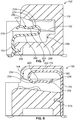
Figure 9 is a cross-sectional view of a portion of the cardedge connector system 100 showing thecircuit card 106 being loaded into thecard edge connector 102 in theloading direction 130.Figure 10 is a cross-sectional view of a portion of the cardedge connector system 100 showing thecircuit card 106 in thecard edge connector 102 in a mated position.Figure 11 is a cross-sectional view of a portion of the cardedge connector system 100 showing thecircuit card 106 in thecard edge connector 102 in a mated position showing thelower contact 152 mated to thecircuit card 106.Figure 12 is a cross-sectional view of a portion of the cardedge connector system 100 showing thecircuit card 106 in thecard edge connector 102 in a mated position showing theupper contact 150 mated to thecircuit card 106. - During loading (
Figure 9 ), thecircuit card 106 is guided into thecard slot 116 by theguide channel 180. Theguide channel 180 is defined by theupper guide surface 182 and thelower guide surface 184. In an exemplary embodiment, the guide surfaces 182, 184 may be angled to allow angled loading of thecircuit card 106 into thecard slot 116 along theangled loading direction 130. Theguide channel 180 guides thecircuit card 106 into the receivingspace 200 between the upper andlower contacts circuit card 106 engages theupper contacts 150 and thelower contact 152, portions of thecontacts spring arms support arms - The
guide pads 186 may define a portion of thelower guide surface 184. Theguide pads 186 elevate thecircuit card 106 off of thelower wall 162 to prevent damage to thelower contacts 152 during loading of thecircuit card 106 into thecard slot 116. - When the
pockets Figure 10 ), thecircuit card 106 may be lowered into thecard slot 116. For example, thelower surface 306 may be dropped below theguide pads 186 to position thecircuit card 106 in thecard slot 116. Once loaded into thecard slot 116, thecircuit card 106 may be lowered in themating direction 132 to the mated position (Figure 10 ). In the mated position, thecircuit card 106 is oriented generally horizontally. As shown inFigure 11 , for example, thespring arm 224 of theupper contact 150 extends along theupper surface 304 for electrical connection with thecorresponding contact pads 308 on theupper surface 304 of thecircuit card 106. As shown inFigure 12 , for example, thespring arm 264 of thelower contact 152 extends along thelower surface 306 for electrical connection with thecorresponding contact pads 308 on thelower surface 306 of thecircuit card 106. -
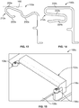
Figure 13 is a side view of theupper contact 150a in accordance with an exemplary embodiment. Themating end 212a of theupper contact 150a is shaped differently than the embodiment illustrated inFigure 4 . Theupper contact 150a includes the first andsecond mating interfaces upper contact 150a includes thesupport arm 222a between the first andsecond mating interfaces support arm 222a may engage the upper wall 160 (shown in phantom) to limit deflection of theupper contact 150a. As such, the first andsecond mating interfaces upper wall 160. -
Figure 14 is a side view of theupper contact 150b in accordance with an exemplary embodiment. The upper contact includes anintermediate section 223b between thesupport arm 222b andspring arm 224b. Theintermediate section 223b adds additional length to themating end 212b of theupper contact 150b. Additionally, thespring arm 224b extends forwardly rather than rearwardly. -
Figure 15 is a perspective view of the cardedge connector system 100c in accordance with an exemplary embodiment.Figure 15 illustrates thecircuit card 106c being secured to thehousing 110c of thecard edge connector 102c using a pair offasteners 108c at the first and second sides of thecircuit card 106c rather than in a middle portion of thecircuit card 106c. Other arrangements of thefasteners 108c are possible in alternative embodiments.
Claims (13)
- A card edge connector (102) comprising:a housing (110) having a mounting end (112) configured to be mounted to a host circuit board (104) and a mating end (114) having a card slot (116) configured to receive a circuit card (106), the housing (110) having an upper wall (160) above the card slot (116) and a lower wall (162) below the card slot (116), the upper wall (160) having upper contact channels (164), the lower wall (162) having lower contact channels (166);upper contacts (150) received in the upper contact channels (164), the upper contacts (150) including corresponding mounting ends (210) and mating ends (212), the mounting ends (210) of the upper contacts (150) extending from the housing (110) for mounting to the host circuit board (104), each mating end (212) of the upper contacts (150) having a first mating interface (230) and a second mating interface (232) remote from the first mating interface (230), the first and second mating interfaces (230, 232) of the upper contacts (150) defining first and second points of contact with the same contact pad (308) on an upper surface (304) of the circuit card (106); andlower contacts (152) received in the lower contact channels (166), the lower contacts (152) including corresponding mounting ends (250) and mating ends (252), the mounting ends (250) of the lower contacts (152) extending from the housing (110) for mounting to the host circuit board (104), each mating end (252) of the lower contacts (152) having a first mating interface (270) and a second mating interface (272) remote from the first mating interface (270), the first and second mating interfaces (270, 272) of the lower contacts (152) defining first and second points of contact with the same contact pad (308) on a lower surface (306) of the circuit card (106).
- The card edge connector (102) of claim 1, wherein the upper contact (150) has a higher spring rate at the first mating interface (230) and a lower spring rate at the second mating interface (232), and wherein the lower contact (152) has a higher spring rate at the first mating interface (270) and a lower spring rate at the second mating interface (272).
- The card edge connector (102) of claim 1 or 2, wherein the lower contacts (152) are shifted forward relative to the upper contacts (150) such that the first and second mating interfaces (270, 272) of the lower contacts (152) are offset with respect to the first and second mating interfaces (230, 232) of the upper contacts (150).
- The card edge connector (102) of any preceding claim, wherein the lower wall (162) is angled nonparallel to the mounting end (112) of the housing (110) to define an angled card slot (116) configured to receive the circuit card (106) in an angled loading direction (130) nonparallel to the host circuit board (104).
- The card edge connector (102) of any preceding claim, wherein the first and second mating interfaces (270, 272) of the lower contacts (152) are arranged along a lower mating plane and the first and second mating interfaces (230, 232) of the upper contacts (150) are arranged along an upper mating plane parallel to the lower mating plane, the card slot (116) being configured to receive the circuit card (106) in a loading direction (130) angled non-parallel to the upper mating plane and the lower mating plane.
- The card edge connector (102) of any preceding claim, further comprising a fastener (108) securely coupled to the housing (110) to secure the circuit card (106) to the housing (110).
- The card edge connector (102) of any preceding claim, wherein the housing (110) includes first and second side walls (172, 174) at first and second sides (126, 128) of the card slot (116), the first and second side walls (172, 174) including guide channels (180) to guide loading of the circuit card (106) into the card slot (116).
- The card edge connector (102) of claim 7, wherein the guide channels (180) are angled nonparallel to the mounting end (112) of the housing (110).
- The card edge connector (102) of any preceding claim, wherein the lower wall (162) includes guide pads (186) at a front of the card slot (116), the guide pads (186) configured to position the circuit card (106) above the lower wall (162) during loading of the circuit card (106) into the card slot (116).
- The card edge connector (102) of claim 9, wherein the guide pads (186) are positioned forward of the first and second mating interfaces (270, 272) of the lower contacts (152) to support the circuit card (106) relative to the lower contacts (152) during loading of the circuit card (106) into the card slot (116).
- The card edge connector (102) of any preceding claim, wherein the housing (110) includes guide wings (192) at first and second sides of the mating end (114) forward of the card slot (116) for guiding the circuit card (106) into the card slot (116).
- The card edge (102) connector of any preceding claim, wherein the upper contact (150) includes a base (214) between the mating end (212) and the mounting end (210) of the upper contact (150), the mating end (212) of the upper contact (150) being cantilevered from the base (214) of the upper contact (150) with a support arm (222) of the upper contact (150) extending from the base (214) of the upper contact (150) and a spring arm (224) extending from the support arm (222) of the upper contact (150), the spring arm (224) of the upper contact (150) being folded under the support arm (222) of the upper contact (150) and defining the first and second mating interfaces (230, 232) of the upper contact (150), and wherein the lower contact (152) includes a base (254) between the mating end (252) and the mounting end (250) of the lower contact (152), the mating end (252) of the lower contact (152) being cantilevered from the base (254) of the lower contact (152) with a support arm (262) of the lower contact (152) extending from the base (254) of the lower contact (152) and a spring arm (264) extending from the support arm (262) of the lower contact (152), the spring arm (264) of the lower contact (152) being folded under the support arm (262)of the lower contact (152) and defining the first and second mating interfaces (270, 272) of the lower contact (152).
- The card edge connector (102) of claim 12, wherein the support arm (222) of the upper contact (150) is flexed relative to the base (214) of the upper contact (150) and the spring arm (224) of the upper contact (150) is flexed toward the support arm (222) of the upper contact (150) when mated with the circuit card (106), and wherein the support arm (262) of the lower contact (152) is flexed relative to the base (254) of the lower contact (152) and the spring arm (264) of the lower contact (152) is flexed toward the support arm (262) of the lower contact (152) when mated with the circuit card (106).
Applications Claiming Priority (1)
| Application Number | Priority Date | Filing Date | Title |
|---|---|---|---|
| US15/867,998 US10811794B2 (en) | 2018-01-11 | 2018-01-11 | Card edge connector system |
Publications (2)
| Publication Number | Publication Date |
|---|---|
| EP3512044A1 true EP3512044A1 (en) | 2019-07-17 |
| EP3512044B1 EP3512044B1 (en) | 2022-05-18 |
Family
ID=65010638
Family Applications (1)
| Application Number | Title | Priority Date | Filing Date |
|---|---|---|---|
| EP19150811.8A Active EP3512044B1 (en) | 2018-01-11 | 2019-01-08 | Card edge connector system |
Country Status (4)
| Country | Link |
|---|---|
| US (1) | US10811794B2 (en) |
| EP (1) | EP3512044B1 (en) |
| CN (1) | CN110034462B (en) |
| CA (1) | CA3028885A1 (en) |
Families Citing this family (3)
| Publication number | Priority date | Publication date | Assignee | Title |
|---|---|---|---|---|
| US11183792B2 (en) * | 2018-06-06 | 2021-11-23 | SK Hynix Inc. | Drive loading jig for memory drives |
| US12322898B2 (en) * | 2019-05-22 | 2025-06-03 | Te Connectivity Solutions Gmbh | Heat sink assembly for an electrical connector assembly |
| US10971863B1 (en) * | 2019-09-25 | 2021-04-06 | Greenconn Corp. | High speed connector assembly and electrical connector thereof |
Citations (5)
| Publication number | Priority date | Publication date | Assignee | Title |
|---|---|---|---|---|
| GB1501255A (en) * | 1975-04-17 | 1978-02-15 | Du Pont Nederland | Electrical contact clip |
| US6482041B1 (en) * | 2001-09-12 | 2002-11-19 | Yen Yu-Feng | Card connector |
| EP2696440A1 (en) * | 2012-08-07 | 2014-02-12 | Kyocera Connector Products Corporation | Connector |
| US20140051294A1 (en) * | 2012-08-15 | 2014-02-20 | Mercury Systems, Inc. | Electrical contact |
| EP3179572A1 (en) * | 2015-12-10 | 2017-06-14 | Iriso Electronics Co., Ltd. | Connector for flat conductor |
Family Cites Families (57)
| Publication number | Priority date | Publication date | Assignee | Title |
|---|---|---|---|---|
| FR1541094A (en) * | 1967-08-23 | 1968-10-04 | Bull General Electric | Improved connectors for printed circuit boards and the like |
| US3920302A (en) * | 1974-05-02 | 1975-11-18 | Johh M Cutchaw | Zero insertion force solderless connector |
| US3941448A (en) * | 1974-07-29 | 1976-03-02 | E. I. Du Pont De Nemours & Company | Connector block |
| US3980377A (en) * | 1975-08-25 | 1976-09-14 | Gte Laboratories Incorporated | Printed circuit connector |
| US4087151A (en) * | 1976-07-28 | 1978-05-02 | Magnetic Controls Company | Printed circuit card edge connector with normalling contacts |
| US4106841A (en) * | 1977-03-11 | 1978-08-15 | Bunker Ramo Corporation | Electrical connector for printed circuit boards |
| US4118094A (en) * | 1977-03-31 | 1978-10-03 | Trw Inc. | Zero-entry force connector |
| US4324451A (en) * | 1979-11-19 | 1982-04-13 | Elfab Corporation | Card edge connector with pull through bellows contact and lay-over insulator |
| US4514030A (en) * | 1981-08-27 | 1985-04-30 | Methode Electronics, Inc. | Shorting edge connector |
| US4705338A (en) * | 1985-12-13 | 1987-11-10 | E. I. Du Pont De Nemours And Company | Zero insertion force connector |
| US4708095A (en) * | 1986-06-16 | 1987-11-24 | Deere & Company | Combined engine cooling and lube system |
| US5071371A (en) * | 1990-03-30 | 1991-12-10 | Molex Incorporated | Electrical card edge connector assembly |
| US5162002A (en) * | 1990-03-30 | 1992-11-10 | Molex Incorporated | Card edge connector assembly |
| US5186643A (en) * | 1991-09-19 | 1993-02-16 | Molex Incorporated | Latching device for an edge connector |
| US5147214A (en) * | 1991-09-27 | 1992-09-15 | Amp Incorporated | Electrical terminal which has overstress protection |
| US5203725A (en) * | 1992-03-16 | 1993-04-20 | Molex Incorporated | Biased edge card connector |
| US5240420A (en) * | 1992-03-31 | 1993-08-31 | Research Organization For Circuit Knowledge | Self-aligning high-density printed circuit connector |
| JPH0629066U (en) * | 1992-09-21 | 1994-04-15 | 京セラエルコ株式会社 | Edge double-sided connector |
| US5277607A (en) * | 1993-01-15 | 1994-01-11 | The Whitaker Corporation | Electrical connector with shorting contacts which wipe against each other |
| US5292265A (en) * | 1993-03-02 | 1994-03-08 | Molex Incorporated | Edge mounted circuit board electrical connector |
| US5415573A (en) * | 1993-07-08 | 1995-05-16 | Molex Incorporated | Edge mounted circuit board electrical connector |
| US5425651A (en) * | 1994-03-04 | 1995-06-20 | The Whitaker Corporation | Card edge connector providing non-simultaneous electrical connections |
| US5514002A (en) * | 1994-04-28 | 1996-05-07 | Hon Hai Precision Ind. Co., Ltd. | Electrical connector assembly and contacts therein |
| JPH08185937A (en) * | 1994-12-28 | 1996-07-16 | Molex Inc | Electric connector for printed-circuit board |
| US5676559A (en) * | 1995-07-06 | 1997-10-14 | The Whitaker Corporation | Zero insertion force (ZIF) electrical connector |
| US5725389A (en) * | 1995-11-09 | 1998-03-10 | Molex Incorporated | Edge card connector |
| US5769668A (en) * | 1996-03-08 | 1998-06-23 | Robinson Nugent, Inc. | Module alignment apparatus for an electrical connector |
| JPH10134910A (en) * | 1996-10-30 | 1998-05-22 | Amp Japan Ltd | Memory card connector and adapter thereof |
| TW347927U (en) * | 1997-07-19 | 1998-12-11 | Speed Tech Corp | Jack connector for random access memory of computer |
| US6015310A (en) * | 1997-12-12 | 2000-01-18 | Molex Incorporated | Electrical connector for flat circuitry |
| US6322370B1 (en) * | 1998-04-16 | 2001-11-27 | Intel Corporation | High speed bus contact system |
| TW399811U (en) * | 1999-02-02 | 2000-07-21 | Hon Hai Prec Ind Co Ltd | Card edge connector |
| JP2002141124A (en) * | 2000-11-02 | 2002-05-17 | Tyco Electronics Amp Kk | Substrate fixing type connector and substrate fixing structure for connector |
| US7204648B2 (en) * | 2002-03-19 | 2007-04-17 | Finisar Corporation | Apparatus for enhancing impedance-matching in a high-speed data communications system |
| US6764345B1 (en) * | 2003-05-27 | 2004-07-20 | Tyco Electronics Corporation | Electrical card edge connector with dual shorting contacts |
| US6955554B2 (en) * | 2004-01-27 | 2005-10-18 | Hon Hai Precision Ind. Co., Ltd. | Electrical connector assembly having board hold down |
| CN1969462B (en) * | 2004-06-15 | 2012-03-28 | 富士通电子零件有限公司 | Transceiver module |
| TWM267702U (en) * | 2004-11-18 | 2005-06-11 | Speed Tech Corp | Card edge connector with position guider |
| US7134896B1 (en) * | 2005-09-30 | 2006-11-14 | Egbon Electronics Ltd. | Latch of a card edge connector |
| CN2874843Y (en) * | 2005-10-31 | 2007-02-28 | 富士康(昆山)电脑接插件有限公司 | Clamp device for card edge connector |
| TWM291121U (en) * | 2005-11-04 | 2006-05-21 | Advanced Connectek Inc | Interface card holding mechanism |
| WO2010039125A1 (en) * | 2008-09-30 | 2010-04-08 | Hewlett-Packard Development Company, L.P. | Dual card connector |
| JP4948574B2 (en) * | 2009-07-24 | 2012-06-06 | 株式会社デンソー | Card edge connector and assembly method thereof |
| US8342733B2 (en) * | 2009-12-14 | 2013-01-01 | Tyco Electronics Corporation | LED lighting assemblies |
| US8282402B2 (en) * | 2009-12-23 | 2012-10-09 | Fci Americas Technology Llc | Card-edge connector |
| TWI519007B (en) * | 2010-04-27 | 2016-01-21 | 泰科資訊科技有限公司 | Stacked card-edge connector and latching members for cards thereof |
| US8690589B2 (en) * | 2010-06-07 | 2014-04-08 | Fci Americas Technology Llc | Electrical card-edge connector |
| US8632365B2 (en) * | 2010-06-07 | 2014-01-21 | Fci Americas Technology Llc | Electrical card-edge connector |
| US20130109240A1 (en) * | 2011-11-01 | 2013-05-02 | Ming -Huang Chiang | Card edge connector |
| US8979558B2 (en) * | 2012-03-12 | 2015-03-17 | Fci Americas Technology Llc | Interposer assembly |
| US9065225B2 (en) * | 2012-04-26 | 2015-06-23 | Apple Inc. | Edge connector having a high-density of contacts |
| CN103682759B (en) * | 2012-09-14 | 2016-05-04 | 富士康(昆山)电脑接插件有限公司 | Bayonet connector and combination thereof |
| TWI614944B (en) * | 2013-01-17 | 2018-02-11 | 星電股份有限公司 | Substrate edge connector |
| JP5481594B1 (en) * | 2013-08-09 | 2014-04-23 | イリソ電子工業株式会社 | Connector terminals and electrical connectors |
| US9318850B2 (en) * | 2014-05-23 | 2016-04-19 | Intel Corporation | Shielding a connector to reduce interference |
| JP5809343B1 (en) * | 2014-10-30 | 2015-11-10 | イリソ電子工業株式会社 | connector |
| CN205657214U (en) * | 2016-04-06 | 2016-10-19 | Afci连接器新加坡私人有限公司 | Electric connector |
-
2018
- 2018-01-11 US US15/867,998 patent/US10811794B2/en active Active
-
2019
- 2019-01-04 CA CA3028885A patent/CA3028885A1/en active Pending
- 2019-01-08 EP EP19150811.8A patent/EP3512044B1/en active Active
- 2019-01-09 CN CN201910018648.4A patent/CN110034462B/en active Active
Patent Citations (5)
| Publication number | Priority date | Publication date | Assignee | Title |
|---|---|---|---|---|
| GB1501255A (en) * | 1975-04-17 | 1978-02-15 | Du Pont Nederland | Electrical contact clip |
| US6482041B1 (en) * | 2001-09-12 | 2002-11-19 | Yen Yu-Feng | Card connector |
| EP2696440A1 (en) * | 2012-08-07 | 2014-02-12 | Kyocera Connector Products Corporation | Connector |
| US20140051294A1 (en) * | 2012-08-15 | 2014-02-20 | Mercury Systems, Inc. | Electrical contact |
| EP3179572A1 (en) * | 2015-12-10 | 2017-06-14 | Iriso Electronics Co., Ltd. | Connector for flat conductor |
Also Published As
| Publication number | Publication date |
|---|---|
| CA3028885A1 (en) | 2019-07-11 |
| CN110034462B (en) | 2022-05-10 |
| EP3512044B1 (en) | 2022-05-18 |
| US20190214754A1 (en) | 2019-07-11 |
| CN110034462A (en) | 2019-07-19 |
| US10811794B2 (en) | 2020-10-20 |
Similar Documents
| Publication | Publication Date | Title |
|---|---|---|
| US10320102B2 (en) | Receptacle connector with contact assembly | |
| US10148025B1 (en) | Header connector of a communication system | |
| US11258214B2 (en) | Compact high speed connector | |
| US9831608B1 (en) | Electrical connector having ground shield that controls impedance at mating interface | |
| US10756467B2 (en) | Circuit card assemblies for a communication system | |
| US8172591B2 (en) | Electrical connector assembly having electrical connector with low profile and processor with cone pins | |
| US10135165B2 (en) | Contact structure for high reliability electrical connector | |
| US11398694B2 (en) | Flex jumper assembly for a plug connector assembly | |
| US10522925B2 (en) | Circuit card assemblies for a communication system | |
| CN109326906B (en) | Electrical contact preloading structure | |
| US10411378B2 (en) | Circuit card assemblies for a communication system | |
| US10856432B1 (en) | Socket connector and cable assembly for a communication system | |
| EP3512044B1 (en) | Card edge connector system | |
| CN118399127A (en) | Card edge connector with connector sleeve | |
| US10096924B2 (en) | Header contact for header connector of a communication system | |
| US12444867B2 (en) | Printed circuit board connector having hermaphroditic contact elements | |
| US12580332B2 (en) | Ground bus for a cable card assembly of an electrical connector | |
| US9461394B2 (en) | Electrical contacts for electrical connectors | |
| US20240178592A1 (en) | Miniaturized high-speed interposer |
Legal Events
| Date | Code | Title | Description |
|---|---|---|---|
| PUAI | Public reference made under article 153(3) epc to a published international application that has entered the european phase |
Free format text: ORIGINAL CODE: 0009012 |
|
| STAA | Information on the status of an ep patent application or granted ep patent |
Free format text: STATUS: THE APPLICATION HAS BEEN PUBLISHED |
|
| AK | Designated contracting states |
Kind code of ref document: A1 Designated state(s): AL AT BE BG CH CY CZ DE DK EE ES FI FR GB GR HR HU IE IS IT LI LT LU LV MC MK MT NL NO PL PT RO RS SE SI SK SM TR |
|
| AX | Request for extension of the european patent |
Extension state: BA ME |
|
| STAA | Information on the status of an ep patent application or granted ep patent |
Free format text: STATUS: REQUEST FOR EXAMINATION WAS MADE |
|
| 17P | Request for examination filed |
Effective date: 20200114 |
|
| RBV | Designated contracting states (corrected) |
Designated state(s): AL AT BE BG CH CY CZ DE DK EE ES FI FR GB GR HR HU IE IS IT LI LT LU LV MC MK MT NL NO PL PT RO RS SE SI SK SM TR |
|
| STAA | Information on the status of an ep patent application or granted ep patent |
Free format text: STATUS: EXAMINATION IS IN PROGRESS |
|
| 17Q | First examination report despatched |
Effective date: 20210325 |
|
| GRAP | Despatch of communication of intention to grant a patent |
Free format text: ORIGINAL CODE: EPIDOSNIGR1 |
|
| STAA | Information on the status of an ep patent application or granted ep patent |
Free format text: STATUS: GRANT OF PATENT IS INTENDED |
|
| RIC1 | Information provided on ipc code assigned before grant |
Ipc: H01R 13/533 20060101ALN20211124BHEP Ipc: H01R 13/24 20060101ALI20211124BHEP Ipc: H01R 12/73 20110101ALI20211124BHEP Ipc: H01R 12/72 20110101AFI20211124BHEP |
|
| INTG | Intention to grant announced |
Effective date: 20211209 |
|
| GRAS | Grant fee paid |
Free format text: ORIGINAL CODE: EPIDOSNIGR3 |
|
| GRAA | (expected) grant |
Free format text: ORIGINAL CODE: 0009210 |
|
| STAA | Information on the status of an ep patent application or granted ep patent |
Free format text: STATUS: THE PATENT HAS BEEN GRANTED |
|
| AK | Designated contracting states |
Kind code of ref document: B1 Designated state(s): AL AT BE BG CH CY CZ DE DK EE ES FI FR GB GR HR HU IE IS IT LI LT LU LV MC MK MT NL NO PL PT RO RS SE SI SK SM TR |
|
| REG | Reference to a national code |
Ref country code: GB Ref legal event code: FG4D |
|
| REG | Reference to a national code |
Ref country code: CH Ref legal event code: EP |
|
| REG | Reference to a national code |
Ref country code: IE Ref legal event code: FG4D |
|
| REG | Reference to a national code |
Ref country code: DE Ref legal event code: R096 Ref document number: 602019014994 Country of ref document: DE |
|
| REG | Reference to a national code |
Ref country code: AT Ref legal event code: REF Ref document number: 1493675 Country of ref document: AT Kind code of ref document: T Effective date: 20220615 |
|
| REG | Reference to a national code |
Ref country code: LT Ref legal event code: MG9D |
|
| REG | Reference to a national code |
Ref country code: NL Ref legal event code: MP Effective date: 20220518 |
|
| REG | Reference to a national code |
Ref country code: AT Ref legal event code: MK05 Ref document number: 1493675 Country of ref document: AT Kind code of ref document: T Effective date: 20220518 |
|
| PG25 | Lapsed in a contracting state [announced via postgrant information from national office to epo] |
Ref country code: SE Free format text: LAPSE BECAUSE OF FAILURE TO SUBMIT A TRANSLATION OF THE DESCRIPTION OR TO PAY THE FEE WITHIN THE PRESCRIBED TIME-LIMIT Effective date: 20220518 Ref country code: PT Free format text: LAPSE BECAUSE OF FAILURE TO SUBMIT A TRANSLATION OF THE DESCRIPTION OR TO PAY THE FEE WITHIN THE PRESCRIBED TIME-LIMIT Effective date: 20220919 Ref country code: NO Free format text: LAPSE BECAUSE OF FAILURE TO SUBMIT A TRANSLATION OF THE DESCRIPTION OR TO PAY THE FEE WITHIN THE PRESCRIBED TIME-LIMIT Effective date: 20220818 Ref country code: NL Free format text: LAPSE BECAUSE OF FAILURE TO SUBMIT A TRANSLATION OF THE DESCRIPTION OR TO PAY THE FEE WITHIN THE PRESCRIBED TIME-LIMIT Effective date: 20220518 Ref country code: LT Free format text: LAPSE BECAUSE OF FAILURE TO SUBMIT A TRANSLATION OF THE DESCRIPTION OR TO PAY THE FEE WITHIN THE PRESCRIBED TIME-LIMIT Effective date: 20220518 Ref country code: HR Free format text: LAPSE BECAUSE OF FAILURE TO SUBMIT A TRANSLATION OF THE DESCRIPTION OR TO PAY THE FEE WITHIN THE PRESCRIBED TIME-LIMIT Effective date: 20220518 Ref country code: GR Free format text: LAPSE BECAUSE OF FAILURE TO SUBMIT A TRANSLATION OF THE DESCRIPTION OR TO PAY THE FEE WITHIN THE PRESCRIBED TIME-LIMIT Effective date: 20220819 Ref country code: FI Free format text: LAPSE BECAUSE OF FAILURE TO SUBMIT A TRANSLATION OF THE DESCRIPTION OR TO PAY THE FEE WITHIN THE PRESCRIBED TIME-LIMIT Effective date: 20220518 Ref country code: ES Free format text: LAPSE BECAUSE OF FAILURE TO SUBMIT A TRANSLATION OF THE DESCRIPTION OR TO PAY THE FEE WITHIN THE PRESCRIBED TIME-LIMIT Effective date: 20220518 Ref country code: BG Free format text: LAPSE BECAUSE OF FAILURE TO SUBMIT A TRANSLATION OF THE DESCRIPTION OR TO PAY THE FEE WITHIN THE PRESCRIBED TIME-LIMIT Effective date: 20220818 Ref country code: AT Free format text: LAPSE BECAUSE OF FAILURE TO SUBMIT A TRANSLATION OF THE DESCRIPTION OR TO PAY THE FEE WITHIN THE PRESCRIBED TIME-LIMIT Effective date: 20220518 |
|
| PG25 | Lapsed in a contracting state [announced via postgrant information from national office to epo] |
Ref country code: RS Free format text: LAPSE BECAUSE OF FAILURE TO SUBMIT A TRANSLATION OF THE DESCRIPTION OR TO PAY THE FEE WITHIN THE PRESCRIBED TIME-LIMIT Effective date: 20220518 Ref country code: PL Free format text: LAPSE BECAUSE OF FAILURE TO SUBMIT A TRANSLATION OF THE DESCRIPTION OR TO PAY THE FEE WITHIN THE PRESCRIBED TIME-LIMIT Effective date: 20220518 Ref country code: LV Free format text: LAPSE BECAUSE OF FAILURE TO SUBMIT A TRANSLATION OF THE DESCRIPTION OR TO PAY THE FEE WITHIN THE PRESCRIBED TIME-LIMIT Effective date: 20220518 Ref country code: IS Free format text: LAPSE BECAUSE OF FAILURE TO SUBMIT A TRANSLATION OF THE DESCRIPTION OR TO PAY THE FEE WITHIN THE PRESCRIBED TIME-LIMIT Effective date: 20220918 |
|
| PG25 | Lapsed in a contracting state [announced via postgrant information from national office to epo] |
Ref country code: SM Free format text: LAPSE BECAUSE OF FAILURE TO SUBMIT A TRANSLATION OF THE DESCRIPTION OR TO PAY THE FEE WITHIN THE PRESCRIBED TIME-LIMIT Effective date: 20220518 Ref country code: SK Free format text: LAPSE BECAUSE OF FAILURE TO SUBMIT A TRANSLATION OF THE DESCRIPTION OR TO PAY THE FEE WITHIN THE PRESCRIBED TIME-LIMIT Effective date: 20220518 Ref country code: RO Free format text: LAPSE BECAUSE OF FAILURE TO SUBMIT A TRANSLATION OF THE DESCRIPTION OR TO PAY THE FEE WITHIN THE PRESCRIBED TIME-LIMIT Effective date: 20220518 Ref country code: EE Free format text: LAPSE BECAUSE OF FAILURE TO SUBMIT A TRANSLATION OF THE DESCRIPTION OR TO PAY THE FEE WITHIN THE PRESCRIBED TIME-LIMIT Effective date: 20220518 Ref country code: DK Free format text: LAPSE BECAUSE OF FAILURE TO SUBMIT A TRANSLATION OF THE DESCRIPTION OR TO PAY THE FEE WITHIN THE PRESCRIBED TIME-LIMIT Effective date: 20220518 Ref country code: CZ Free format text: LAPSE BECAUSE OF FAILURE TO SUBMIT A TRANSLATION OF THE DESCRIPTION OR TO PAY THE FEE WITHIN THE PRESCRIBED TIME-LIMIT Effective date: 20220518 |
|
| REG | Reference to a national code |
Ref country code: DE Ref legal event code: R097 Ref document number: 602019014994 Country of ref document: DE |
|
| PLBE | No opposition filed within time limit |
Free format text: ORIGINAL CODE: 0009261 |
|
| STAA | Information on the status of an ep patent application or granted ep patent |
Free format text: STATUS: NO OPPOSITION FILED WITHIN TIME LIMIT |
|
| PG25 | Lapsed in a contracting state [announced via postgrant information from national office to epo] |
Ref country code: AL Free format text: LAPSE BECAUSE OF FAILURE TO SUBMIT A TRANSLATION OF THE DESCRIPTION OR TO PAY THE FEE WITHIN THE PRESCRIBED TIME-LIMIT Effective date: 20220518 |
|
| 26N | No opposition filed |
Effective date: 20230221 |
|
| PG25 | Lapsed in a contracting state [announced via postgrant information from national office to epo] |
Ref country code: SI Free format text: LAPSE BECAUSE OF FAILURE TO SUBMIT A TRANSLATION OF THE DESCRIPTION OR TO PAY THE FEE WITHIN THE PRESCRIBED TIME-LIMIT Effective date: 20220518 |
|
| REG | Reference to a national code |
Ref country code: CH Ref legal event code: PL |
|
| PG25 | Lapsed in a contracting state [announced via postgrant information from national office to epo] |
Ref country code: LU Free format text: LAPSE BECAUSE OF NON-PAYMENT OF DUE FEES Effective date: 20230108 |
|
| REG | Reference to a national code |
Ref country code: BE Ref legal event code: MM Effective date: 20230131 |
|
| PG25 | Lapsed in a contracting state [announced via postgrant information from national office to epo] |
Ref country code: LI Free format text: LAPSE BECAUSE OF NON-PAYMENT OF DUE FEES Effective date: 20230131 Ref country code: CH Free format text: LAPSE BECAUSE OF NON-PAYMENT OF DUE FEES Effective date: 20230131 |
|
| PG25 | Lapsed in a contracting state [announced via postgrant information from national office to epo] |
Ref country code: BE Free format text: LAPSE BECAUSE OF NON-PAYMENT OF DUE FEES Effective date: 20230131 |
|
| PG25 | Lapsed in a contracting state [announced via postgrant information from national office to epo] |
Ref country code: IT Free format text: LAPSE BECAUSE OF FAILURE TO SUBMIT A TRANSLATION OF THE DESCRIPTION OR TO PAY THE FEE WITHIN THE PRESCRIBED TIME-LIMIT Effective date: 20220518 Ref country code: IE Free format text: LAPSE BECAUSE OF NON-PAYMENT OF DUE FEES Effective date: 20230108 |
|
| PG25 | Lapsed in a contracting state [announced via postgrant information from national office to epo] |
Ref country code: MC Free format text: LAPSE BECAUSE OF FAILURE TO SUBMIT A TRANSLATION OF THE DESCRIPTION OR TO PAY THE FEE WITHIN THE PRESCRIBED TIME-LIMIT Effective date: 20220518 |
|
| PG25 | Lapsed in a contracting state [announced via postgrant information from national office to epo] |
Ref country code: MC Free format text: LAPSE BECAUSE OF FAILURE TO SUBMIT A TRANSLATION OF THE DESCRIPTION OR TO PAY THE FEE WITHIN THE PRESCRIBED TIME-LIMIT Effective date: 20220518 |
|
| PG25 | Lapsed in a contracting state [announced via postgrant information from national office to epo] |
Ref country code: BG Free format text: LAPSE BECAUSE OF FAILURE TO SUBMIT A TRANSLATION OF THE DESCRIPTION OR TO PAY THE FEE WITHIN THE PRESCRIBED TIME-LIMIT Effective date: 20220518 |
|
| PG25 | Lapsed in a contracting state [announced via postgrant information from national office to epo] |
Ref country code: BG Free format text: LAPSE BECAUSE OF FAILURE TO SUBMIT A TRANSLATION OF THE DESCRIPTION OR TO PAY THE FEE WITHIN THE PRESCRIBED TIME-LIMIT Effective date: 20220518 |
|
| PG25 | Lapsed in a contracting state [announced via postgrant information from national office to epo] |
Ref country code: CY Free format text: LAPSE BECAUSE OF FAILURE TO SUBMIT A TRANSLATION OF THE DESCRIPTION OR TO PAY THE FEE WITHIN THE PRESCRIBED TIME-LIMIT; INVALID AB INITIO Effective date: 20190108 |
|
| PG25 | Lapsed in a contracting state [announced via postgrant information from national office to epo] |
Ref country code: HU Free format text: LAPSE BECAUSE OF FAILURE TO SUBMIT A TRANSLATION OF THE DESCRIPTION OR TO PAY THE FEE WITHIN THE PRESCRIBED TIME-LIMIT; INVALID AB INITIO Effective date: 20190108 |
|
| REG | Reference to a national code |
Ref country code: GB Ref legal event code: 732E Free format text: REGISTERED BETWEEN 20250731 AND 20250806 |
|
| PG25 | Lapsed in a contracting state [announced via postgrant information from national office to epo] |
Ref country code: TR Free format text: LAPSE BECAUSE OF FAILURE TO SUBMIT A TRANSLATION OF THE DESCRIPTION OR TO PAY THE FEE WITHIN THE PRESCRIBED TIME-LIMIT Effective date: 20220518 |
|
| PGFP | Annual fee paid to national office [announced via postgrant information from national office to epo] |
Ref country code: GB Payment date: 20251204 Year of fee payment: 8 |
|
| PGFP | Annual fee paid to national office [announced via postgrant information from national office to epo] |
Ref country code: FR Payment date: 20251208 Year of fee payment: 8 |
|
| PGFP | Annual fee paid to national office [announced via postgrant information from national office to epo] |
Ref country code: DE Payment date: 20251203 Year of fee payment: 8 |