EP3512037A1 - A compact annular slot type antenna - Google Patents
A compact annular slot type antenna Download PDFInfo
- Publication number
- EP3512037A1 EP3512037A1 EP18305022.8A EP18305022A EP3512037A1 EP 3512037 A1 EP3512037 A1 EP 3512037A1 EP 18305022 A EP18305022 A EP 18305022A EP 3512037 A1 EP3512037 A1 EP 3512037A1
- Authority
- EP
- European Patent Office
- Prior art keywords
- antenna
- conductive
- layer
- conductive surface
- slots
- Prior art date
- Legal status (The legal status is an assumption and is not a legal conclusion. Google has not performed a legal analysis and makes no representation as to the accuracy of the status listed.)
- Withdrawn
Links
Images


Classifications
-
- H—ELECTRICITY
- H01—ELECTRIC ELEMENTS
- H01Q—ANTENNAS, i.e. RADIO AERIALS
- H01Q1/00—Details of, or arrangements associated with, antennas
- H01Q1/48—Earthing means; Earth screens; Counterpoises
-
- H—ELECTRICITY
- H01—ELECTRIC ELEMENTS
- H01Q—ANTENNAS, i.e. RADIO AERIALS
- H01Q1/00—Details of, or arrangements associated with, antennas
- H01Q1/36—Structural form of radiating elements, e.g. cone, spiral, umbrella; Particular materials used therewith
- H01Q1/38—Structural form of radiating elements, e.g. cone, spiral, umbrella; Particular materials used therewith formed by a conductive layer on an insulating support
-
- H—ELECTRICITY
- H01—ELECTRIC ELEMENTS
- H01Q—ANTENNAS, i.e. RADIO AERIALS
- H01Q13/00—Waveguide horns or mouths; Slot antennas; Leaky-waveguide antennas; Equivalent structures causing radiation along the transmission path of a guided wave
- H01Q13/10—Resonant slot antennas
Definitions
- the present disclosure relates to an antenna adapted to be integrated in an apparatus for receiving a digital signal.
- a slot antenna consists of a metalized surface with one or more holes or slots cut out.
- the slot radiates electromagnetic waves in a way similar to a dipole antenna.
- the shape and the size of the slot determine the radiation pattern.
- Annular slot antenna (ASA) are examples of known slot antenna wherein the slot is annular.
- the ASA is an interesting simple, low cost, easy to manufacture planar microstrip printed antenna with a compact shape factor and almost an omnidirectional radiation pattern when used with a finite ground plane.
- the operating frequency range of the ASA remains relatively limited though better than the patch antenna.
- a printed monopole antenna is another simple low cost known antenna presenting a wider operating frequency range than the ASA, but generally requiring a larger ground plane. Integrating a printed monopole antenna in a device also raises coupling issues with the rest of the circuits of the device. Another issue of ASA-type antennas is their tendency to radiate in the broadside direction, i.e. in the orthogonal direction to the plane of the antenna. The present disclosure has been designed with the foregoing in mind.
- a novel antenna topology is proposed.
- the novel antenna topology is realized for example in a printed circuit board comprising at least a first and a second layer, the first layer being essentially non-conductive, the second layer being essentially conductive.
- a microstrip line is etched in the first layer, and a non-conductive surface is etched in the second layer within a conductive area.
- the second layer further comprises a number of slots, wherein each of the slots extends the non-conductive surface towards an edge of the second layer.
- the novel antenna called compact annular slot type antenna preserves some interesting properties of the known annular slot antenna while improving the operating frequency range, and the radiation pattern in the plane of the printed circuit board direction compared to the annular slot antenna.
- the printed circuit board antenna comprises a first layer and a second layer, the first layer comprising a conductive track the second layer comprising a non-conductive surface within a conductive area and a number of slots, wherein each of the slots extends the non-conductive surface towards an edge of the second layer.
- the number of slots is one among two, four, six and eight.
- the slots have a same length.
- the slots have different lengths.
- the slots are straight lines or triangular.
- the non-conductive surface has an annular form.
- the first layer further comprises a conductive surface fed by the conductive track, one of either the conductive surface or the non-conductive surface surrounding the other, the conductive surface and the non-conductive surface being centred in the plane of the printed circuit board antenna.
- the conductive surface and the non-conductive surface have a same shape.
- the shape belongs to a set comprising a, triangle, a square, a rectangle, an ellipse, a polygon, a ripple.
- the non-conductive surface and the conductive surface form an interval of a constant width in the plane of the printed circuit board.
- the first layer is a top layer of the printed circuit board antenna.
- the second layer is a bottom layer of the printed circuit board antenna.
- the printed circuit board comprises a third layer with a second non-conductive surface within a second conductive area, one of either the second non-conductive surface or the non-conductive surface surrounding the other, the second non-conductive surface and the non-conductive surface being centred in the plane of the printed circuit board antenna.
- a digital television receiver integrating an antenna according any of the above variant is also disclosed.
- the present embodiments may be employed in any combination or sub-combination.
- the present principles are not limited to the described variants, and any arrangement of variants and embodiments can be used.
- the present principles are not limited to the described shape examples and any other type of shape, is compatible with the disclosed principles.
- the present principles are not further limited to the described numbers of layers of the printed circuit board antenna and are applicable to any arrangement of any number of layers of a printed circuit board antenna.
- the present principles are further not limited to the described shape, number, position and length of the slots extending the non-conductive surface towards the edges of the printed circuit board antenna, and are applicable to any other shape, number, position and length of the slots.
- Figure 1 illustrates an annular slot antenna according to the prior art.
- Figure 1 shows three schematic views of the ASA 10.
- the two left hand views 10A, 10B represent respectively a top side 10A and a bottom side 10B of the ASA 10.
- the right-hand view represents the elements present both at the top and bottom sides of the ASA 10.
- the bottom side of the ASA 10 is a conductive ground plane 12 comprising an annular slot 110.
- the top side of the ASA is a non-conductive substrate 11 comprising a metallized microstrip line 120. When the metallized microstrip line 120 is driven by a signal at a given frequency, the annular slot 110 radiates electronic waves in a way similar to a dipole antenna.
- the slot nature of the ASA presents also some interesting features, such as, the easy integration of active devices in the slot for radiation pattern or frequency reconfiguration of the antenna.
- Another advantage of a slot antenna such as the ASA is the natural decoupling between the antenna and the rest of the circuits which could be realized either on the space available backside of the ground plane where the radiating slot is etched or on a separate printed circuit board (PCB) which is shielded by the slot ground plane.
- PCB printed circuit board
- slot is used throughout the disclosed principles to refer to a non-conductive area etched in a conductive area within a same layer of for example a PCB.
- the slot represents a hole cut out of for example a metal surface.
- FIG 7A shows an example of a compact annular slot type antenna 70 according to a specific and non-limiting embodiment of the disclosed principles.
- the compact annular slot type antenna 70 is for example a printed circuit board antenna comprising a first layer and a second layer.
- the second layer comprises a non-conductive surface 710 within a conductive area 72.
- the non-conductive surface illustrated at Figures 7A is an annular slot, but any other shape of slot is compatible with the disclosed principles.
- the non-conductive surface 710 is for example etched from a fully conductive layer. In other words, the second layer is fully conductive except the surface 710 being etched in the conductive layer.
- the second layer further comprises a number of non-conductive slots 711, 712, 713, 714 within the conductive area 72, wherein each non-conductive slot 711, 712, 713, 714 extends the non-conductive surface 710 within the conductive area 72 towards an edge of the second layer.
- the illustrated compact annular slot type antenna 70 comprises four straight slots, but any number of slots, including single slot embodiments, and/or any other shape of slot are compatible with the disclosed principles. According to different variants of the disclosed principles the number of slots of the compact annular slot type antenna 70 is among two, four, six or eight.
- the printed circuit board i.e. including the first and the second layers
- the slots extend the non-conductive surface towards the corners of the square.
- other embodiments with different PCB shapes and/or where the slots extend the non-conductive surface towards an edge of the PCB anywhere between two corners of the PCB are also compatible with the disclosed principles.
- the first layer of the PCB comprises a conductive track 720 within a non-conductive area (not shown), the conductive track being driven by a signal, wherein an extremity 721 of the conductive track 720 extends beyond the crossing point by a length such that to optimize the power transmission of the driving signal from the conductive track to the slot-type antenna
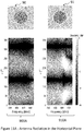
- Figures 7A and 7B further show a comparison of the radiation directivity of the compact annular slot type antenna 70 with the radiation directivity of an existing regular ASA antenna 10 of a similar shape and size respectively in the plane of the PCB including the antenna (i.e. Horizontal Plane) and in an orthogonal plane of the PCB antenna (Vertical Plane) More precisely, Figure 7A illustrates two 2D directivity radiation patterns 100A, 700A in the plane of the PCB (Horizontal Plane), as a function of the frequency, of respectively an existing regular ASA antenna 10 and a compact annular slot type antenna 70 according to a non-limiting embodiment of the disclosed principles.
- Figure 7B illustrates two 2D directivity radiation patterns 100B, 700B in a plane orthogonal to the plane of the PCB (Vertical Plane) as a function of the frequency of respectively an existing regular ASA antenna 10 and a compact annular slot type antenna 70 according to a non-limiting embodiment of the disclosed principles.
- Regular ASA type antenna 10 are known to tend to radiate in the broadside direction (direction orthogonal to the PCB of the ASA type antenna).
- the PCB is considered horizontally positioned, the PCB plane is called the horizontal plane and the plane orthogonal to the PCB place is called the vertical plane.
- the propensity of the ASA type antenna 10 to radiate more in the vertical plane appears on Figures 7A and 7B where the directivity radiation pattern 100B (in the vertical plane) is overall brighter (more directive) than the directivity radiation pattern 100A in the horizontal plane.
- Figure 7A further shows the improved directivity radiation pattern 700A according to the disclosed principles compared to 100A in the horizontal plane, being generally brighter, especially in the frequencies between 400 and 600 MHz.
- the improved radiation pattern is obtained in the horizontal plane thanks to the slots extending the non-conductive surface towards edges of the PCB.
- Figure 7B further illustrates that the directivity radiation pattern 700B is not degraded in the vertical plane, compared to the directivity radiation pattern 100B.
- Figure 8 shows five examples of antenna according to five specific and non-limiting embodiments of the disclosed principles.
- the compact annular slot type antenna 80 is a printed circuit board antenna comprising a first layer and a second layer.
- the second layer comprises a non-conductive surface 810 within a conductive area 82 (similar to the non-conductive area 72 described at Figures 7A and 7B ).
- the non-conductive surface illustrated here is an annular slot, but any other shape of slot is compatible with the disclosed principles.
- the second layer further comprises a number of non-conductive slots 811, 812, 813, 814 within the conductive area 82, wherein each non-conductive slot 811, 812, 813, 814 extends the non-conductive surface 810 within the conductive area 82 towards an edge of the second layer.
- the illustrated compact annular slot type antenna 80 comprises triangular slots 811, 812, 813, 814 wherein each triangular slot is based on an edge of the second layer, and directed towards the non-conductive surface 810.
- the triangular slots 811, 812, 813, 814 of the antenna 80 are extending the non-conductive surface towards the edges of the second layer, similarly to the straight slots 711, 712, 713, 714 of the antenna 70.
- Each triangular slot 811, 812, 813, 814 is connected to the non-conductive surface 810 via a corner opposite to the base located at the edge of the second layer.
- the illustrated antenna 80 comprises four triangular slots, but any number of triangular slots, including single triangular slot embodiments, are compatible with the disclosed principles. According to different variants of the disclosed principles the number of slots of the compact annular slot type antenna 80 is among two, four, six or eight. According to the illustrated and non-limiting embodiment, the printed circuit board (i.e. including the first and the second layers) is squarish, and each triangular slot extends the non-conductive surface towards the middle of an edge of the square. But other embodiments with different PCB shape and/or where the slots extend the non-conductive surface towards an edge of the second layer anywhere between two corners of the second layer are also compatible with the disclosed principles.
- the first layer of the PCB comprises a conductive track 820 within a non-conductive area (not shown), the conductive track being driven by a signal, wherein an extremity of the conductive track 820 extends beyond the crossing point of 810 by a length such that to optimize the power transmission of the driving signal from the conductive track 820 to the slot-type antenna.
- Figure 8 shows four further examples of compact annular slot type antenna 81, 82, 83, 84, according to different variants.
- Figure 8 shows three examples of compact annular slot type antenna 81, 83, 84 with non-conductive surfaces of different shapes, being respectively a polygon, a ripple and a square.
- Figure 8 shows two examples of compact annular slot type antenna 81, 82 with different terminating positions of the slots in the edges of the PCB, not being the middle of the edge, nor a corner of the square.
- Figure 8 shows also an example of a compact annular slot type antenna 82, with a different orientation of the microstrip line of the first layer.
- the HMS antenna 20 is a printed circuit board antenna comprising a first layer 20A and a second layer 20B separated by a non-conductive substrate.
- the first layer 20A comprises a conductive track 221 feeding a conductive surface 220.
- the first layer is for example made of a non-conductive substrate 21, on which a conductive track such as a microstrip line 221 and a conductive surface 220 are printed, the conductive track 221 being connected to the conductive surface 220.
- the conductive track and the conductive surface are etched on the PCB.
- the conductive track and the conductive surface are stuck on the PCB.
- the conductive surface is for example a metallized surface of any shape, for example a disc shape as illustrated.
- Figure 2 shows the microstrip line and the conductive surface as the only conductive elements printed on the non-conductive substrate.
- any first layer comprising other conductive elements such as conductive tracks between components or circuits (not represented in Figure 2 ) are also compatible with the disclosed principles.
- the second layer 20B comprises a non-conductive surface 210 embedded in a conductive area.
- the conductive area at least surrounds the non-conductive surface.
- the non-conductive surface 210 is for example etched from a fully conductive layer 22.
- the second layer 20B is fully conductive except the surface 210 being etched in the conductive layer 22.
- Partially conductive layers for example, comprising areas of conductive surfaces (wherein one of them surrounds the non-conductive surface), although not being fully conductive are also compatible with the disclosed principles.
- the second layer needs only to be sufficiently conductive to serve for example as a ground layer in a PCB.
- one of either the conductive surface 220 or the non-conductive surface 210 is surrounding the other, the conductive surface 220 and the non-conductive surface 210 being centred in the plane of the printed circuit board antenna 20.
- An interval 211 between the non-conductive surface 210 and the conductive surface 220 results from one of either the conductive surface 220 or the non-conductive surface 210 being surrounding the other.
- surrounding it is meant here and throughout the document that one surface is overlapping the other in the plane of the PCB. In other words, when looking at projections of both surfaces in the plane of the PCB, one projected surface is completely included in the other.
- the interval between the non-conductive surface 210 and the conductive surface 220 of different layers of the PCB antenna behaves as a slot antenna by radiating electromagnetic waves.
- the interval although behaving as a slot differs from a slot as an interval is a hole between conductive surfaces of different layers while a slot is a hole within a conductive surface of same layer.
- the non-conductive surface 210 is surrounding the conductive surface 220 in the plane of the PCB, forming an interval 211 between the conductive 220 and the non-conductive 210 surfaces. Said differently, a projection of the conductive surface 220 in the plane of the PCB is included in the projection of the non-conductive surface 210 in the same plane of the PCB.
- the conductive surface 220 is surrounding the non-conductive surface 210 in the plane of the PCB, also forming an interval 211 between the conductive 220 and the non-conductive 210 surfaces.
- the interval between 211 between the conductive 220 and the non-conductive 210 surfaces of the HMS antenna behaves as a slot in a slot antenna, by radiating electromagnetic waves when the conductive track is driven by a signal.
- the conductive surface 220 and the non-conductive surface 210 have a same shape, being a disc (as represented in Figure 2 ).
- Other shapes are compatible with the disclosed principles.
- a HMS antenna with a conductive surface and a non-conductive surface of different shapes, wherein one of the surface is surrounding the other, is also compatible the disclosed principles.
- the HMS antenna 20 is composed of a microstrip line fed circular conductive disc 220 etched on one side of a PCB and a circular non-conductive disc slot 210 realized on the other side (the ground side) of the substrate.
- the sizing of the HMS antenna is so that the non-conductive circular disc slot 210 and the conductive circular disc 220 are aligned in the (x,y) plane, while the diameter of the first is 10 mm larger than the diameter of the second and so that the interval 211 generated between the circular disc etched on one side of the substrate and the circular slot realized on the other side presents almost the same dimensions as the slot of a regular ASA.
- Figure 3A and 3B show simulation results for a HMS antenna designed for a central frequency around 600MHz, according to a specific and non-limiting embodiment.
- the PCB is a square of 300mm by 300mm.
- the diameter of the disc (conductive surface) is 160 mm.
- the width of the interval between both discs is constant and about 5 mm.
- Figure 3A shows proposed antenna input reflection coefficient magnitude in dB compared from one side, to an "equivalent" regular ASA (with the exact same dimensions and excited through microstrip to slot line quarter-wave transition) and, on the other side a monopole (with the same dimensions and ground-disc distance of 5mm).
- the HMS antenna has a performance similar to an ASA however with a wider bandwidth. This can also be seen from the radiation efficiency given in Figure 3B , showing a comparison of the radiation efficiency over the frequency band for the HMS, the ASA and the monopole antenna.
- the Monopole antenna shows a wider radiation efficiency than the ASA or the HMS, it does not provide the same advantages as the ASA.
- the HMS antenna is advantageous compared to the existing antenna because it preserves the advantages of the ASA (omnidirectional pattern, natural decoupling of the antenna with the rest of the circuits) and provides an increased radiation efficiency compared to the ASA.
- the HMS antenna provides the same omnidirectional radiation pattern as the ASA, the same natural decoupling properties with an increased radiation efficiency in the lower frequencies, the HMS antenna is a very good omnidirectional antenna solution for being integrated in a device.
- Figure 4 shows five examples of HMS antenna 4A, 4B, 4C, 4D, 4E, according to five specific and non-limiting embodiments of the disclosed principles. All the HMS examples illustrated at Figure 4 represent conductive and non-conductive surfaces of a same shape, wherein the shape is a triangle 4A, a square 4B, a polygon 4C, an ellipse 4D or a ripple 4E.
- Figure 5 shows three examples of HMS antenna 5A, 5B, 5C according to three specific and non-limiting embodiments of the disclosed principles.
- Figure 5 shows two HMS antenna 5A, 5B wherein the PCB is a square.
- Figure 5 shows a HMS antenna 5C wherein the PCB is a polygon.
- Figure 5 also illustrates different positions and length of the conductive track connected to the conductive surface.
- Figure 6 shows four examples of HMS antenna 6A, 6B, 6C, 6D according to four specific and non-limiting embodiments of the disclosed principles. While Figures 2 , 4 and 5 show HMS antenna with an interval between the conductive and the non-conductive surfaces of a constant width, the HMS antenna 6A, 6B, 6C, 6D comprise an interval 211 between the conductive and the non-conductive surfaces of variable width in the plane of the HMS antenna. Moreover, the HMS antenna 6C and 6D comprise conductive surfaces and non-conductive surfaces of different shapes. Adjusting the shape, and/or the width of the interval allow for example to further finetune some other characteristics of the antenna such as for example and without limitation the frequency adaptation, the radiating pattern, frequency band efficiency.
- Figures 9A and 9B illustrate the electrical field distribution of a HMS antenna 90 at two different frequencies, according to a specific and non-limiting embodiment of the disclosed principles. More precisely Figure 9A illustrates the electrical field (E-field) distribution E of the hybrid monopole slot antenna 90 at the frequency of 600 MHz. At this frequency, the perimeter 900 of the annular interval is almost equal to ⁇ g , where ⁇ g is the guided wavelength in the interval, and the antenna behaves as two slightly curved half-wave slot dipoles connected in the virtual short circuit, represented as SC plane in Figure 9A , with the maxima of the electrical field, in the plane cutting the middle of the dipoles, corresponding to the virtual open circuit plane, represented as OC plane in Figure 9A , orthogonal to the SC plane.
- SC plane virtual short circuit
- Figure 9B schematically presents the electrical field (E-field) distribution of the same HMS antenna 90, at the frequency of around 200 MHz.
- the perimeter 900 of the annular interval is smaller than ⁇ g /2, where ⁇ g is the guided wavelength in the interval and the E-field distribution is sketched in Figure 9B with the maximum at the opposite side of the excitation point 901 and decreasing close to zero at the excitation point 901. Therefore, the E-field at both sides of the ⁇ plane partly cancel each other (destructive combination) leading to a poor antenna radiation efficiency at this frequency.
- FIGS 9C and 9D illustrate two examples of compact hybrid monopole slot antenna according to two specific and non-limiting embodiments of the disclosed principles.
- the compact hybrid monopole slot antenna 91 and 92 similarly to the HMS antenna previously described at figures 2 , 4 , 5 and 6 , comprise a first layer and a second layer.
- the first layer comprises a conductive surface fed by a conductive track within a non-conductive area.
- the second layer comprises a non-conductive surface within a conductive area, wherein one of either the conductive surface or the non-conductive surface is surrounding the other, the conductive surface and the non-conductive surface being centred in the plane of the printed circuit board antenna.
- the compact hybrid monopole slot antenna 91, 92 further comprises a number of slots, wherein each of the slots extends the non-conductive surface towards an edge of the second layer.
- the addition of slots to the HMS antenna allows to further reduce the size of the HMS antenna, as explained below. This is why HMS antenna comprising slots extending the non-conductive surface towards edges of the second layer are called compact HMS antenna.
- Figures 9C and 9D illustrate a compact HMS antenna 91, 92 with four slots, but any number of slots is compatible with the disclosed principles.
- Figures 9C and 9D respectively illustrate two examples of compact HMS antenna with straight slots and triangular slots.
- the variants described for the compact ASA type antenna are also applicable to the compact HMS antenna.
- Figures 9E and 9F further illustrate the impact of the slots on the E-field distribution. Although illustrated only for the straight slots, the impact is similar for triangular slots. As slots extend the non-conductive surface in the second layer towards the edges of the second layer, the location and the length of the slots are chosen so that at the operating frequency, a significant part of the power migrates from the annular interval to the added slots.
- Figure 9F i.e. at frequency around 200 MHz, where the perimeter is smaller than ⁇ g /2)
- the generated E-fields constructively combine with the residual E-field resulting from the annular interval, therefore improving the radiation efficiency of the antenna at the low edge of the frequency band for which, the perimeter of the interval is smaller than ⁇ g /2).
- Figure 9E i.e.
- Figures 10A and 10B show simulation results for two examples of antenna according to two specific and non-limiting embodiments of the disclosed principles. More precisely, Figure 10A presents the simulated radiation efficiency of an example of a compact HMS antenna 91 (i.e. HMS with four additional straight slots) with an example of a HMS antenna 90 (without additional slots). This result confirms the expected improvement of the radiation efficiency of a HMS antenna at low frequencies, due to the additional slots. Indeed, the radiation efficiency rises from 20% (with 90) to 60 % (with 91) at 200 MHz. A side effect of adding the slots is a small degradation of the antenna radiation efficiency around 650 MHz.
- this minor degradation is due to the fact that the E-field resulting from the additional slots partially cancels the E-field generated by the annular interval.
- This degradation can be adjusted in frequency and amplitude by adjusting the position and the length of the slots in the second layer.
- the resulting band notch can be further leveraged to reduce interferences taking place at the notch frequency.
- Figure 10B presents the simulated radiation efficiency of another example of a compact HMS antenna 92 (i.e. HMS with four additional triangular slots) with an example of a HMS antenna 90 (without additional slots).
- This result shows a similar improvement of the radiation efficiency in the lower frequencies, which is an important result as it allows to reduce the size of the antenna and makes it easier to integrate in a device.
- the simulations further show an attenuated notch around 650Mhz compared to the variant with straight slots shown in Figure 10A .
- Figures 11 A and 11B show a comparison of the radiation directivity of a compact HMS antenna 91 (with additional slots) with the radiation directivity of a HMS antenna 90 (without additional slots) respectively in the plane of the antenna and in an orthogonal plane of the antenna. More precisely Figure 11 A illustrates two 2D directivity radiation patterns 900A, 910A in the plane of the PCB, as a function of the frequency, of respectively a HMS antenna 90 (without additional slots) and a compact HMS antenna 91 (with four additional straight slots) according to two non-limiting embodiments of the disclosed principles.
- Figure 11B illustrates two 2D directivity radiation patterns 900B, 910B in a plane orthogonal to the plane of the PCB as a function of the frequency of respectively a HMS antenna 90 (without additional slots) and a compact HMS antenna 91 (with four additional straight slots) according to two non-limiting embodiments of the disclosed principles.
- the HMS antenna 90 exhibits similar radiation patterns 900A, 900B as a regular ASA type antenna 10. Indeed, the radiation patterns 100A, 100B of Figures 7A , 7B are respectively similar to the radiation patterns 900A, 900B in Figures 11 A, 11B. Extending the non-conductive surface of the second layer by additional slots towards the edges of the second layer provides the same improvement of the radiation pattern directivity in the horizontal plane for the compact HMS antenna (with additional slots) compared to the HMS antenna (without additional slot).
- Figure 12 shows six examples of antenna according to six specific and non-limiting embodiments of the disclosed principles.
- Figure 12 shows two examples 121, 122 of compact HMS antenna comprising two straight slots, wherein the straight slots are at different positions for the two embodiments.
- Figure 12 shows four examples 123, 124, 125, 126 of compact HMS antenna comprising four straight slots, with different shapes of non- conductive surfaces, and therefore different shapes of intervals.
- the slots extending the non-conductive surface of the second layer are at different positions and have different lengths. Similar embodiment with triangular slots are compatible with the disclosed principles.
- the first layer is the top layer of the printed circuit board antenna
- the second layer is the bottom layer of the printed circuit board antenna.
- the top and bottom layers are the two external layers of the PCB, being respectively the front and the back side of the PCB.
- the disclosed principles are not limited to PCBs with the first and the second layers being external layers. Any PCB wherein one or both of the first and the second layers are internal layers of the PCB is also compatible with the disclosed principles.
- the PCB antenna according to any embodiment and/or variant previously described, comprises a third layer with a second non-conductive surface embedded in a second conductive area, the second non-conductive surface being centred with the surface and the non-conductive surface, the second non-conductive surface surrounding at least one of the conductive and the non-conductive surfaces in the plane of the printed circuit board antenna.
- the second non-conductive surface surrounds only one of either the conductive or the non-conductive surfaces in the plane of the printed circuit board antenna.
- the surface being surrounded by the second non-conductive surface is the smaller surface.
- the second non-conductive surface surrounds only both the conductive or the non-conductive surfaces in the plane of the printed circuit board antenna.
- the second non-conductive surface and the non-conductive surface have different sizes. Adding such additional layers comprising further non-conductive surfaces as described above allows to further expand the frequency band of the antenna by multiplying resonators to neighbouring frequencies.
- the antenna is designed for a central frequency around 600MHz, corresponding for example to a digital terrestrial transmission frequency band.
- the PCB antenna according to any corresponding embodiment and/or variant previously described is a square of 300mm by 300mm, the diameter of the conductive disc (conductive surface) is for example 160 mm, and the diameter of the non-conductive disc is 170 mm.
- This antenna design is for example well suited for being integrated in digital TV receivers so that the TV receivers, with integrated HMS antenna are adapted for an indoor TV reception without requiring any external or outdoor antenna.
- the integration a HMS antenna directly in a digital TV receiver allows for easier deployment of digital TV receivers by avoiding the need of any external outdoor antenna solution.
- the HMS antenna is further compatible with other frequency bands and suited for being integrated in other communications devices such as cell phones, Wi-Fi devices, and wireless access points of any wireless standard.
- the antenna is designed for a central frequency around 5GHz, for example corresponding to Wi-Fi devices.
- the dimensions of antenna are adapted to another frequency band by applying a ratio on its dimensions corresponding to the ratio of the central frequencies (here for example 600/5000).
- a HMS antenna designed for the 5GHz band would fit in a PCB square of 36 mm by 36 mm and the diameters of the conductive disc and non-conductive discs being respectively of 19 mm and 20.5 mm.
- Such an antenna device can be integrated in wireless devices such a cell phones, Wi-Fi cards or Wi-Fi access points. Any HMS design with dimensions adapted to a targeted frequency is compatible with the disclosed principles.
Landscapes
- Details Of Aerials (AREA)
- Waveguide Aerials (AREA)
Abstract
A novel antenna topology is proposed. The novel antenna topology is realized for example in a printed circuit board comprising at least a first and a second layer, the first layer being essentially non-conductive, the second layer being essentially conductive. A microstrip line is etched in the first layer, and a non-conductive surface is etched in the second layer within a conductive area. The second layer further comprises a number of slots, wherein each of the slots extends the non-conductive surface towards an edge of the second layer. The novel antenna called compact annular slot type antenna preserves some interesting properties of the known annular slot antenna while improving the operating frequency range, and the radiation pattern in the plane of the printed circuit board direction compared to the annular slot antenna.
Description
- The present disclosure relates to an antenna adapted to be integrated in an apparatus for receiving a digital signal.
- A slot antenna consists of a metalized surface with one or more holes or slots cut out. When the metalized surface is driven as an antenna by a driving frequency, the slot radiates electromagnetic waves in a way similar to a dipole antenna. The shape and the size of the slot determine the radiation pattern. Annular slot antenna (ASA) are examples of known slot antenna wherein the slot is annular. The ASA is an interesting simple, low cost, easy to manufacture planar microstrip printed antenna with a compact shape factor and almost an omnidirectional radiation pattern when used with a finite ground plane. Despite of other interesting properties such as a natural decoupling between the antenna and the rest of the circuits thanks to the metalized surface, the operating frequency range of the ASA remains relatively limited though better than the patch antenna. A printed monopole antenna is another simple low cost known antenna presenting a wider operating frequency range than the ASA, but generally requiring a larger ground plane. Integrating a printed monopole antenna in a device also raises coupling issues with the rest of the circuits of the device. Another issue of ASA-type antennas is their tendency to radiate in the broadside direction, i.e. in the orthogonal direction to the plane of the antenna. The present disclosure has been designed with the foregoing in mind.
- A novel antenna topology is proposed. The novel antenna topology is realized for example in a printed circuit board comprising at least a first and a second layer, the first layer being essentially non-conductive, the second layer being essentially conductive. A microstrip line is etched in the first layer, and a non-conductive surface is etched in the second layer within a conductive area. The second layer further comprises a number of slots, wherein each of the slots extends the non-conductive surface towards an edge of the second layer. The novel antenna called compact annular slot type antenna preserves some interesting properties of the known annular slot antenna while improving the operating frequency range, and the radiation pattern in the plane of the printed circuit board direction compared to the annular slot antenna.
- To that end a printed circuit board antenna is disclosed. The printed circuit board antenna comprises a first layer and a second layer, the first layer comprising a conductive track the second layer comprising a non-conductive surface within a conductive area and a number of slots, wherein each of the slots extends the non-conductive surface towards an edge of the second layer.
- According to variant, the number of slots is one among two, four, six and eight.
- According to another variant, the slots have a same length.
- According to another variant, the slots have different lengths.
- According to another variant, the slots are straight lines or triangular.
- According to another variant, the non-conductive surface has an annular form.
- According to another variant, the first layer further comprises a conductive surface fed by the conductive track, one of either the conductive surface or the non-conductive surface surrounding the other, the conductive surface and the non-conductive surface being centred in the plane of the printed circuit board antenna.
- According to another variant, the conductive surface and the non-conductive surface have a same shape.
- According to another variant, the shape belongs to a set comprising a, triangle, a square, a rectangle, an ellipse, a polygon, a ripple.
- According to another variant, the non-conductive surface and the conductive surface form an interval of a constant width in the plane of the printed circuit board.
- According to another variant, the first layer is a top layer of the printed circuit board antenna.
- According to another variant, the second layer is a bottom layer of the printed circuit board antenna.
- According to another variant, the printed circuit board comprises a third layer with a second non-conductive surface within a second conductive area, one of either the second non-conductive surface or the non-conductive surface surrounding the other, the second non-conductive surface and the non-conductive surface being centred in the plane of the printed circuit board antenna.
- In a second aspect, a digital television receiver integrating an antenna according any of the above variant is also disclosed.
- While not explicitly described, the present embodiments may be employed in any combination or sub-combination. For example, the present principles are not limited to the described variants, and any arrangement of variants and embodiments can be used. Moreover, the present principles are not limited to the described shape examples and any other type of shape, is compatible with the disclosed principles. The present principles are not further limited to the described numbers of layers of the printed circuit board antenna and are applicable to any arrangement of any number of layers of a printed circuit board antenna. The present principles are further not limited to the described shape, number, position and length of the slots extending the non-conductive surface towards the edges of the printed circuit board antenna, and are applicable to any other shape, number, position and length of the slots.
-
-
Figure 1 illustrates an annular slot antenna according to the prior art; -
Figure 2 shows a hybrid monopole slot antenna according to a specific and non-limiting embodiment of the disclosed principles; -
Figures 3A and 3B shows simulation results for a hybrid monopole slot antenna, according to a specific and non-limiting embodiment; -
Figure 4 shows five examples of antenna according to five specific and non-limiting embodiments of the disclosed principles; -
Figure 5 shows three further examples of antenna according to three specific and non-limiting embodiments of the disclosed principles; -
Figure 6 shows four further examples of antenna according to four specific and non-limiting embodiments of the disclosed principles; -
Figures 7A and7B illustrate an example of an antenna according to a specific and non-limiting embodiment of the disclosed principles together with a comparison of a radiation directivity of a compact annular slot type antenna with a radiation directivity of an ASA antenna respectively in the plane of the antenna and in an orthogonal plane of the antenna; -
Figure 8 shows five examples of antenna according to five specific and non-limiting embodiments of the disclosed principles; -
Figures 9A and 9B illustrate the electrical field distribution of a hybrid monopole slot antenna at two different frequencies; -
Figures 9C and 9D illustrate two examples of antenna according to two specific and non-limiting embodiments of the disclosed principles; -
Figures 9E and 9F illustrate the electrical field distribution of a hybrid monopole slot antenna according to a specific and non-limiting embodiment of the disclosed principles, at the same two different frequencies asFigures 9A and 9B ; -
Figures 10A and 10B show simulation results for the two examples of antenna ofFigures 9C and 9D ; -
Figures 11 A and 11B illustrate two examples of antenna according to two specific and non-limiting embodiments of the disclosed principles together with a comparison between their radiation directivity respectively in the plane of the printed circuit board antenna and in an orthogonal plane of the antenna; -
Figure 12 shows six examples of antenna according to six specific and non-limiting embodiments of the disclosed principles. - It should be understood that the drawing(s) are for purposes of illustrating the concepts of the disclosure and are not necessarily the only possible configuration for illustrating the disclosure.
- The present description illustrates the principles of the present disclosure. All examples and conditional language recited herein are intended for educational purposes to aid the reader in understanding the principles of the disclosure and the concepts contributed by the inventor to furthering the art, and are to be construed as being without limitation to such specifically recited examples and conditions.
- Moreover, all statements herein reciting principles, aspects, and embodiments of the disclosure, as well as specific examples thereof, are intended to encompass both structural and functional equivalents thereof. Additionally, it is intended that such equivalents include both currently known equivalents as well as equivalents developed in the future, i.e., any elements developed that perform the same function, regardless of structure. Thus, for example, it will be appreciated by those skilled in the art that the block diagrams presented herein represent conceptual views of illustrative circuitry embodying the principles of the disclosure.
-
Figure 1 illustrates an annular slot antenna according to the prior art.Figure 1 shows three schematic views of theASA 10. The two left hand views 10A, 10B represent respectively atop side 10A and abottom side 10B of theASA 10. The right-hand view represents the elements present both at the top and bottom sides of theASA 10. The bottom side of theASA 10 is aconductive ground plane 12 comprising anannular slot 110. The top side of the ASA is anon-conductive substrate 11 comprising a metallizedmicrostrip line 120. When the metallizedmicrostrip line 120 is driven by a signal at a given frequency, theannular slot 110 radiates electronic waves in a way similar to a dipole antenna. The slot nature of the ASA presents also some interesting features, such as, the easy integration of active devices in the slot for radiation pattern or frequency reconfiguration of the antenna. Another advantage of a slot antenna such as the ASA is the natural decoupling between the antenna and the rest of the circuits which could be realized either on the space available backside of the ground plane where the radiating slot is etched or on a separate printed circuit board (PCB) which is shielded by the slot ground plane. This makes the ASA antenna a good candidate for being integrated in electronic devices such as communication devices. - The term "slot" is used throughout the disclosed principles to refer to a non-conductive area etched in a conductive area within a same layer of for example a PCB. The slot represents a hole cut out of for example a metal surface.
-
Figure 7A shows an example of a compact annularslot type antenna 70 according to a specific and non-limiting embodiment of the disclosed principles. The compact annularslot type antenna 70 is for example a printed circuit board antenna comprising a first layer and a second layer. The second layer comprises anon-conductive surface 710 within aconductive area 72. The non-conductive surface illustrated atFigures 7A is an annular slot, but any other shape of slot is compatible with the disclosed principles. Thenon-conductive surface 710 is for example etched from a fully conductive layer. In other words, the second layer is fully conductive except thesurface 710 being etched in the conductive layer. Partially conductive layers, for example, comprising areas of conductive surfaces (wherein one of them surrounds the non-conductive surface), although not being fully conductive are also compatible with the disclosed principles. The second layer further comprises a number ofnon-conductive slots conductive area 72, wherein eachnon-conductive slot non-conductive surface 710 within theconductive area 72 towards an edge of the second layer. The illustrated compact annularslot type antenna 70 comprises four straight slots, but any number of slots, including single slot embodiments, and/or any other shape of slot are compatible with the disclosed principles. According to different variants of the disclosed principles the number of slots of the compact annularslot type antenna 70 is among two, four, six or eight. According to the illustrated and non-limiting embodiment, the printed circuit board (i.e. including the first and the second layers) is squarish, and the slots extend the non-conductive surface towards the corners of the square. But other embodiments with different PCB shapes and/or where the slots extend the non-conductive surface towards an edge of the PCB anywhere between two corners of the PCB are also compatible with the disclosed principles. - The first layer of the PCB comprises a
conductive track 720 within a non-conductive area (not shown), the conductive track being driven by a signal, wherein anextremity 721 of theconductive track 720 extends beyond the crossing point by a length such that to optimize the power transmission of the driving signal from the conductive track to the slot-type antenna -
Figures 7A and7B further show a comparison of the radiation directivity of the compact annularslot type antenna 70 with the radiation directivity of an existingregular ASA antenna 10 of a similar shape and size respectively in the plane of the PCB including the antenna (i.e. Horizontal Plane) and in an orthogonal plane of the PCB antenna (Vertical Plane) More precisely,Figure 7A illustrates two 2Ddirectivity radiation patterns regular ASA antenna 10 and a compact annularslot type antenna 70 according to a non-limiting embodiment of the disclosed principles. Similarly,Figure 7B illustrates two 2Ddirectivity radiation patterns regular ASA antenna 10 and a compact annularslot type antenna 70 according to a non-limiting embodiment of the disclosed principles. - Regular
ASA type antenna 10 are known to tend to radiate in the broadside direction (direction orthogonal to the PCB of the ASA type antenna). For the sake of clarity and without loss of generality, the PCB is considered horizontally positioned, the PCB plane is called the horizontal plane and the plane orthogonal to the PCB place is called the vertical plane. The propensity of theASA type antenna 10 to radiate more in the vertical plane appears onFigures 7A and7B where thedirectivity radiation pattern 100B (in the vertical plane) is overall brighter (more directive) than thedirectivity radiation pattern 100A in the horizontal plane.Figure 7A further shows the improveddirectivity radiation pattern 700A according to the disclosed principles compared to 100A in the horizontal plane, being generally brighter, especially in the frequencies between 400 and 600 MHz. The improved radiation pattern is obtained in the horizontal plane thanks to the slots extending the non-conductive surface towards edges of the PCB.Figure 7B further illustrates that thedirectivity radiation pattern 700B is not degraded in the vertical plane, compared to thedirectivity radiation pattern 100B. -
Figure 8 shows five examples of antenna according to five specific and non-limiting embodiments of the disclosed principles. According to a first example, the compact annularslot type antenna 80 is a printed circuit board antenna comprising a first layer and a second layer. The second layer comprises anon-conductive surface 810 within a conductive area 82 (similar to thenon-conductive area 72 described atFigures 7A and7B ). The non-conductive surface illustrated here is an annular slot, but any other shape of slot is compatible with the disclosed principles. The second layer further comprises a number ofnon-conductive slots conductive area 82, wherein eachnon-conductive slot non-conductive surface 810 within theconductive area 82 towards an edge of the second layer. The illustrated compact annularslot type antenna 80 comprisestriangular slots non-conductive surface 810. Thetriangular slots antenna 80 are extending the non-conductive surface towards the edges of the second layer, similarly to thestraight slots antenna 70. Eachtriangular slot non-conductive surface 810 via a corner opposite to the base located at the edge of the second layer. - The illustrated
antenna 80 comprises four triangular slots, but any number of triangular slots, including single triangular slot embodiments, are compatible with the disclosed principles. According to different variants of the disclosed principles the number of slots of the compact annularslot type antenna 80 is among two, four, six or eight. According to the illustrated and non-limiting embodiment, the printed circuit board (i.e. including the first and the second layers) is squarish, and each triangular slot extends the non-conductive surface towards the middle of an edge of the square. But other embodiments with different PCB shape and/or where the slots extend the non-conductive surface towards an edge of the second layer anywhere between two corners of the second layer are also compatible with the disclosed principles. - The first layer of the PCB comprises a
conductive track 820 within a non-conductive area (not shown), the conductive track being driven by a signal, wherein an extremity of theconductive track 820 extends beyond the crossing point of 810 by a length such that to optimize the power transmission of the driving signal from theconductive track 820 to the slot-type antenna. -
Figure 8 shows four further examples of compact annularslot type antenna Figure 8 shows three examples of compact annularslot type antenna Figure 8 shows two examples of compact annularslot type antenna Figure 8 shows also an example of a compact annularslot type antenna 82, with a different orientation of the microstrip line of the first layer. -
Figure 2 shows a Hybrid Monopole Slot (HMS) antenna according to a specific and non-limiting embodiment of the disclosed principles. According to the specific and non-limiting embodiment, theHMS antenna 20 is a printed circuit board antenna comprising afirst layer 20A and asecond layer 20B separated by a non-conductive substrate. Thefirst layer 20A comprises aconductive track 221 feeding aconductive surface 220. The first layer is for example made of anon-conductive substrate 21, on which a conductive track such as amicrostrip line 221 and aconductive surface 220 are printed, theconductive track 221 being connected to theconductive surface 220. In another example, the conductive track and the conductive surface are etched on the PCB. In yet another example, the conductive track and the conductive surface are stuck on the PCB. The conductive surface is for example a metallized surface of any shape, for example a disc shape as illustrated.Figure 2 shows the microstrip line and the conductive surface as the only conductive elements printed on the non-conductive substrate. However, any first layer comprising other conductive elements such as conductive tracks between components or circuits (not represented inFigure 2 ) are also compatible with the disclosed principles. Thesecond layer 20B comprises anon-conductive surface 210 embedded in a conductive area. The conductive area at least surrounds the non-conductive surface. Thenon-conductive surface 210 is for example etched from a fullyconductive layer 22. In other words, thesecond layer 20B is fully conductive except thesurface 210 being etched in theconductive layer 22. Partially conductive layers, for example, comprising areas of conductive surfaces (wherein one of them surrounds the non-conductive surface), although not being fully conductive are also compatible with the disclosed principles. The second layer needs only to be sufficiently conductive to serve for example as a ground layer in a PCB. - According to the specific and non-limiting embodiment of the disclosed principles, one of either the
conductive surface 220 or thenon-conductive surface 210 is surrounding the other, theconductive surface 220 and thenon-conductive surface 210 being centred in the plane of the printedcircuit board antenna 20. Aninterval 211 between thenon-conductive surface 210 and theconductive surface 220 results from one of either theconductive surface 220 or thenon-conductive surface 210 being surrounding the other. By "surrounding" it is meant here and throughout the document that one surface is overlapping the other in the plane of the PCB. In other words, when looking at projections of both surfaces in the plane of the PCB, one projected surface is completely included in the other. The interval between thenon-conductive surface 210 and theconductive surface 220 of different layers of the PCB antenna behaves as a slot antenna by radiating electromagnetic waves. The interval although behaving as a slot, differs from a slot as an interval is a hole between conductive surfaces of different layers while a slot is a hole within a conductive surface of same layer. - According to a first variant, (represented in
Figure 2 ), thenon-conductive surface 210 is surrounding theconductive surface 220 in the plane of the PCB, forming aninterval 211 between the conductive 220 and the non-conductive 210 surfaces. Said differently, a projection of theconductive surface 220 in the plane of the PCB is included in the projection of thenon-conductive surface 210 in the same plane of the PCB. According to a second variant (not represented inFigure 2 ), theconductive surface 220 is surrounding thenon-conductive surface 210 in the plane of the PCB, also forming aninterval 211 between the conductive 220 and the non-conductive 210 surfaces. The interval between 211 between the conductive 220 and the non-conductive 210 surfaces of the HMS antenna behaves as a slot in a slot antenna, by radiating electromagnetic waves when the conductive track is driven by a signal. - According to this specific and non-limiting embodiment, the
conductive surface 220 and thenon-conductive surface 210 have a same shape, being a disc (as represented inFigure 2 ). Other shapes (as represented further inFigures 4 and6 ) are compatible with the disclosed principles. Moreover, a HMS antenna with a conductive surface and a non-conductive surface of different shapes, wherein one of the surface is surrounding the other, is also compatible the disclosed principles. - According to the specific variant, the
HMS antenna 20 is composed of a microstrip line fed circularconductive disc 220 etched on one side of a PCB and a circularnon-conductive disc slot 210 realized on the other side (the ground side) of the substrate. The sizing of the HMS antenna is so that the non-conductivecircular disc slot 210 and the conductivecircular disc 220 are aligned in the (x,y) plane, while the diameter of the first is 10 mm larger than the diameter of the second and so that theinterval 211 generated between the circular disc etched on one side of the substrate and the circular slot realized on the other side presents almost the same dimensions as the slot of a regular ASA. -
Figure 3A and 3B show simulation results for a HMS antenna designed for a central frequency around 600MHz, according to a specific and non-limiting embodiment. - The antenna is printed on a commonly used FR4 (Flame Resistant 4) substrate (εr = 4.2, tan(δ) = 0.02) with a thickness of 1.041 mm. The PCB is a square of 300mm by 300mm. The diameter of the disc (conductive surface) is 160 mm. The width of the interval between both discs is constant and about 5 mm.
Figure 3A shows proposed antenna input reflection coefficient magnitude in dB compared from one side, to an "equivalent" regular ASA (with the exact same dimensions and excited through microstrip to slot line quarter-wave transition) and, on the other side a monopole (with the same dimensions and ground-disc distance of 5mm). As it can be noticed, the HMS antenna has a performance similar to an ASA however with a wider bandwidth. This can also be seen from the radiation efficiency given inFigure 3B , showing a comparison of the radiation efficiency over the frequency band for the HMS, the ASA and the monopole antenna. Although the Monopole antenna shows a wider radiation efficiency than the ASA or the HMS, it does not provide the same advantages as the ASA. The HMS antenna is advantageous compared to the existing antenna because it preserves the advantages of the ASA (omnidirectional pattern, natural decoupling of the antenna with the rest of the circuits) and provides an increased radiation efficiency compared to the ASA. Increasing the radiation efficiency in the lower frequencies (around 200 MHz) is particularly interesting as it allows to reduce the size of the antenna (for a same level of performance) facilitating its integration in a device. As the HMS antenna provides the same omnidirectional radiation pattern as the ASA, the same natural decoupling properties with an increased radiation efficiency in the lower frequencies, the HMS antenna is a very good omnidirectional antenna solution for being integrated in a device. -
Figure 4 shows five examples ofHMS antenna Figure 4 represent conductive and non-conductive surfaces of a same shape, wherein the shape is atriangle 4A, a square 4B, apolygon 4C, anellipse 4D or aripple 4E. -
Figure 5 shows three examples ofHMS antenna Figure 5 shows twoHMS antenna Figure 5 shows aHMS antenna 5C wherein the PCB is a polygon.Figure 5 also illustrates different positions and length of the conductive track connected to the conductive surface. -
Figure 6 shows four examples ofHMS antenna Figures 2 ,4 and 5 show HMS antenna with an interval between the conductive and the non-conductive surfaces of a constant width, theHMS antenna interval 211 between the conductive and the non-conductive surfaces of variable width in the plane of the HMS antenna. Moreover, theHMS antenna -
Figures 9A and 9B illustrate the electrical field distribution of aHMS antenna 90 at two different frequencies, according to a specific and non-limiting embodiment of the disclosed principles. More preciselyFigure 9A illustrates the electrical field (E-field) distributionE of the hybridmonopole slot antenna 90 at the frequency of 600 MHz. At this frequency, theperimeter 900 of the annular interval is almost equal to λg, where λg is the guided wavelength in the interval, and the antenna behaves as two slightly curved half-wave slot dipoles connected in the virtual short circuit, represented as SC plane inFigure 9A , with the maxima of the electrical field, in the plane cutting the middle of the dipoles, corresponding to the virtual open circuit plane, represented as OC plane inFigure 9A , orthogonal to the SC plane. Due to the phase change of the electrical field distribution over a wavelength, while the E-field in the upper half of the annular interval (above the SC plane) is directed from the inner disc to the ground plane, in the lower half, it is directed from the ground to the inner disc. Therefore, the electrical fields constructively combine giving rise to a good antenna radiation efficiency. -
Figure 9B schematically presents the electrical field (E-field) distribution of thesame HMS antenna 90, at the frequency of around 200 MHz. At this frequency, theperimeter 900 of the annular interval is smaller than λg/2, where λg is the guided wavelength in the interval and the E-field distribution is sketched inFigure 9B with the maximum at the opposite side of theexcitation point 901 and decreasing close to zero at theexcitation point 901. Therefore, the E-field at both sides of the π plane partly cancel each other (destructive combination) leading to a poor antenna radiation efficiency at this frequency. -
Figures 9C and 9D illustrate two examples of compact hybrid monopole slot antenna according to two specific and non-limiting embodiments of the disclosed principles. The compact hybridmonopole slot antenna figures 2 ,4 ,5 and6 , comprise a first layer and a second layer. The first layer comprises a conductive surface fed by a conductive track within a non-conductive area. The second layer comprises a non-conductive surface within a conductive area, wherein one of either the conductive surface or the non-conductive surface is surrounding the other, the conductive surface and the non-conductive surface being centred in the plane of the printed circuit board antenna. According to this specific and non-limiting embodiment, the compact hybridmonopole slot antenna Figures 9C and 9D illustrate acompact HMS antenna Figures 9C and 9D respectively illustrate two examples of compact HMS antenna with straight slots and triangular slots. The variants described for the compact ASA type antenna are also applicable to the compact HMS antenna. -
Figures 9E and 9F further illustrate the impact of the slots on the E-field distribution. Although illustrated only for the straight slots, the impact is similar for triangular slots. As slots extend the non-conductive surface in the second layer towards the edges of the second layer, the location and the length of the slots are chosen so that at the operating frequency, a significant part of the power migrates from the annular interval to the added slots. InFigure 9F (i.e. at frequency around 200 MHz, where the perimeter is smaller than λg/2)the generated E-fields constructively combine with the residual E-field resulting from the annular interval, therefore improving the radiation efficiency of the antenna at the low edge of the frequency band for which, the perimeter of the interval is smaller than λg/2). However inFigure 9E (i.e. at frequency around 600 MHz, where the perimeter is almost equal to λg), thetotal E-field 911 E resulting from the annular interval (illustrated in black onFigure 9E ), partly cancels the E-field 910E generated by the added slots (illustrated in white onFigure 9E ). -
Figures 10A and 10B show simulation results for two examples of antenna according to two specific and non-limiting embodiments of the disclosed principles. More precisely,Figure 10A presents the simulated radiation efficiency of an example of a compact HMS antenna 91 (i.e. HMS with four additional straight slots) with an example of a HMS antenna 90 (without additional slots). This result confirms the expected improvement of the radiation efficiency of a HMS antenna at low frequencies, due to the additional slots. Indeed, the radiation efficiency rises from 20% (with 90) to 60 % (with 91) at 200 MHz. A side effect of adding the slots is a small degradation of the antenna radiation efficiency around 650 MHz. As explained above, this minor degradation is due to the fact that the E-field resulting from the additional slots partially cancels the E-field generated by the annular interval. This degradation can be adjusted in frequency and amplitude by adjusting the position and the length of the slots in the second layer. The resulting band notch can be further leveraged to reduce interferences taking place at the notch frequency. -
Figure 10B presents the simulated radiation efficiency of another example of a compact HMS antenna 92 (i.e. HMS with four additional triangular slots) with an example of a HMS antenna 90 (without additional slots). This result shows a similar improvement of the radiation efficiency in the lower frequencies, which is an important result as it allows to reduce the size of the antenna and makes it easier to integrate in a device. The simulations further show an attenuated notch around 650Mhz compared to the variant with straight slots shown inFigure 10A . -
Figures 11 A and 11B show a comparison of the radiation directivity of a compact HMS antenna 91 (with additional slots) with the radiation directivity of a HMS antenna 90 (without additional slots) respectively in the plane of the antenna and in an orthogonal plane of the antenna. More preciselyFigure 11 A illustrates two 2Ddirectivity radiation patterns Figure 11B illustrates two 2Ddirectivity radiation patterns - The HMS antenna 90 (without additional slots) exhibits
similar radiation patterns ASA type antenna 10. Indeed, theradiation patterns Figures 7A ,7B are respectively similar to theradiation patterns Figures 11 A, 11B. Extending the non-conductive surface of the second layer by additional slots towards the edges of the second layer provides the same improvement of the radiation pattern directivity in the horizontal plane for the compact HMS antenna (with additional slots) compared to the HMS antenna (without additional slot). -
Figure 12 shows six examples of antenna according to six specific and non-limiting embodiments of the disclosed principles.Figure 12 shows two examples 121, 122 of compact HMS antenna comprising two straight slots, wherein the straight slots are at different positions for the two embodiments.Figure 12 shows four examples 123, 124, 125, 126 of compact HMS antenna comprising four straight slots, with different shapes of non- conductive surfaces, and therefore different shapes of intervals. Depending on the embodiments illustrated atFigure 12 , the slots extending the non-conductive surface of the second layer are at different positions and have different lengths. Similar embodiment with triangular slots are compatible with the disclosed principles. - According to a variant (not illustrated), the first layer is the top layer of the printed circuit board antenna, and/or the second layer is the bottom layer of the printed circuit board antenna. The top and bottom layers are the two external layers of the PCB, being respectively the front and the back side of the PCB. The disclosed principles are not limited to PCBs with the first and the second layers being external layers. Any PCB wherein one or both of the first and the second layers are internal layers of the PCB is also compatible with the disclosed principles.
- According to another variant (not illustrated), the PCB antenna according to any embodiment and/or variant previously described, comprises a third layer with a second non-conductive surface embedded in a second conductive area, the second non-conductive surface being centred with the surface and the non-conductive surface, the second non-conductive surface surrounding at least one of the conductive and the non-conductive surfaces in the plane of the printed circuit board antenna. In a first variant the second non-conductive surface surrounds only one of either the conductive or the non-conductive surfaces in the plane of the printed circuit board antenna. In that first variant, the surface being surrounded by the second non-conductive surface is the smaller surface. In a second variant the second non-conductive surface surrounds only both the conductive or the non-conductive surfaces in the plane of the printed circuit board antenna. According to that second variant, the second non-conductive surface and the non-conductive surface have different sizes. Adding such additional layers comprising further non-conductive surfaces as described above allows to further expand the frequency band of the antenna by multiplying resonators to neighbouring frequencies.
- According to a specific and non-limiting embodiment, the antenna is designed for a central frequency around 600MHz, corresponding for example to a digital terrestrial transmission frequency band. The PCB antenna, according to any corresponding embodiment and/or variant previously described is a square of 300mm by 300mm, the diameter of the conductive disc (conductive surface) is for example 160 mm, and the diameter of the non-conductive disc is 170 mm. This antenna design is for example well suited for being integrated in digital TV receivers so that the TV receivers, with integrated HMS antenna are adapted for an indoor TV reception without requiring any external or outdoor antenna. The integration a HMS antenna directly in a digital TV receiver allows for easier deployment of digital TV receivers by avoiding the need of any external outdoor antenna solution. The HMS antenna is further compatible with other frequency bands and suited for being integrated in other communications devices such as cell phones, Wi-Fi devices, and wireless access points of any wireless standard. According to another specific and non-limiting embodiment, the antenna is designed for a central frequency around 5GHz, for example corresponding to Wi-Fi devices. To a first approximation, the dimensions of antenna are adapted to another frequency band by applying a ratio on its dimensions corresponding to the ratio of the central frequencies (here for example 600/5000). According to this specific and non-limiting embodiment, a HMS antenna designed for the 5GHz band would fit in a PCB square of 36 mm by 36 mm and the diameters of the conductive disc and non-conductive discs being respectively of 19 mm and 20.5 mm. Such an antenna device can be integrated in wireless devices such a cell phones, Wi-Fi cards or Wi-Fi access points. Any HMS design with dimensions adapted to a targeted frequency is compatible with the disclosed principles.
Claims (15)
- A printed circuit board antenna (20, 4A, 4B, 4C, 4D, 4E, 5A, 5B, 5C, 6A, 6B, 6C, 6D, 70, 80, 90, 91, 92, 121, 122, 123, 124, 125, 126) comprising a first layer and a second layer, the first layer comprising a conductive track (221, 720, 820) the second layer comprising a non-conductive surface (210, 710, 810) within a conductive area (22, 72, 82) and a number of slots (711, 712, 713, 714, 811, 812, 813, 814), wherein each of the slots (711,712, 713, 714, 811, 812, 813, 814) extends the non-conductive surface (210, 710, 810) towards an edge of the second layer.
- The antenna according to claim 1, wherein the number of slots is one among two, four, six and eight.
- The antenna according to any of claims 1 to 2, wherein the slots have a same length.
- The antenna according to any of claims 1 to 2, wherein the slots have different lengths.
- The antenna according to any of claims 1 to 4, wherein the slots are straight lines.
- The antenna according to any of claims 1 to 5, wherein the slots are triangular.
- The antenna according to any of claims 1 to 6, wherein the non-conductive surface has an annular form.
- The antenna according to any of claims 1 to 6, wherein the first layer further comprises a conductive surface (220) fed by the conductive track (221), one of either the conductive surface (220) or the non-conductive surface (210, 710, 810) surrounding the other, the conductive surface (220) and the non-conductive surface (210, 710, 810) being centred in the plane of the printed circuit board antenna.
- The antenna according to claim 8, wherein the conductive surface (220) and the non-conductive surface (210, 710, 810) have a same shape.
- The antenna according to claim 9, wherein the shape belongs to a set comprising a, triangle, a square, a rectangle, an ellipse, a polygon, a ripple.
- The antenna according to claim 9, wherein the non-conductive surface (210, 710, 810) and the conductive surface (220) form an interval (211) of a constant width in the plane of the printed circuit board.
- The antenna according to any of claims 1 to 11, wherein the first layer is a top layer of the printed circuit board antenna.
- The antenna according to any of claims 1 to 12, wherein the second layer is a bottom layer of the printed circuit board antenna.
- The antenna according to any of claims 1 to 13 wherein the printed circuit board comprises a third layer with a second non-conductive surface within a second conductive area, one of either the second non-conductive surface or the non-conductive surface surrounding the other, the second non-conductive surface and the non-conductive surface being centred in the plane of the printed circuit board antenna.
- A digital television receiver integrating an antenna according to any of claims 1 to 14.
Priority Applications (1)
| Application Number | Priority Date | Filing Date | Title |
|---|---|---|---|
| EP18305022.8A EP3512037A1 (en) | 2018-01-12 | 2018-01-12 | A compact annular slot type antenna |
Applications Claiming Priority (1)
| Application Number | Priority Date | Filing Date | Title |
|---|---|---|---|
| EP18305022.8A EP3512037A1 (en) | 2018-01-12 | 2018-01-12 | A compact annular slot type antenna |
Publications (1)
| Publication Number | Publication Date |
|---|---|
| EP3512037A1 true EP3512037A1 (en) | 2019-07-17 |
Family
ID=61027620
Family Applications (1)
| Application Number | Title | Priority Date | Filing Date |
|---|---|---|---|
| EP18305022.8A Withdrawn EP3512037A1 (en) | 2018-01-12 | 2018-01-12 | A compact annular slot type antenna |
Country Status (1)
| Country | Link |
|---|---|
| EP (1) | EP3512037A1 (en) |
Citations (2)
| Publication number | Priority date | Publication date | Assignee | Title |
|---|---|---|---|---|
| JPS51101447A (en) * | 1975-03-05 | 1976-09-07 | Tokyo Shibaura Electric Co | |
| EP3168930A1 (en) * | 2014-08-29 | 2017-05-17 | Huawei Technologies Co. Ltd. | Antenna and communication device |
-
2018
- 2018-01-12 EP EP18305022.8A patent/EP3512037A1/en not_active Withdrawn
Patent Citations (2)
| Publication number | Priority date | Publication date | Assignee | Title |
|---|---|---|---|---|
| JPS51101447A (en) * | 1975-03-05 | 1976-09-07 | Tokyo Shibaura Electric Co | |
| EP3168930A1 (en) * | 2014-08-29 | 2017-05-17 | Huawei Technologies Co. Ltd. | Antenna and communication device |
Similar Documents
| Publication | Publication Date | Title |
|---|---|---|
| US11431087B2 (en) | Wideband, low profile, small area, circular polarized UHF antenna | |
| US10854994B2 (en) | Broadband phased array antenna system with hybrid radiating elements | |
| US10490346B2 (en) | Antenna structures having planar inverted F-antenna that surrounds an artificial magnetic conductor cell | |
| US11545761B2 (en) | Dual-band cross-polarized 5G mm-wave phased array antenna | |
| US8525741B2 (en) | Multi-loop antenna system and electronic apparatus having the same | |
| US9871301B2 (en) | Integrated miniature PIFA with artificial magnetic conductor metamaterials | |
| US9825357B2 (en) | Electronic device including patch antenna assembly having capacitive feed points and spaced apart conductive shielding vias and related methods | |
| US7106264B2 (en) | Broadband slot antenna and slot array antenna using the same | |
| US8723751B2 (en) | Antenna system with planar dipole antennas and electronic apparatus having the same | |
| KR101164618B1 (en) | Microstrip stacked patch array antenna | |
| US7129899B2 (en) | Antenna | |
| US20100066622A1 (en) | Multi-sector antenna | |
| CN107636895B (en) | Antenna system and antenna module with reduced interference between radiation patterns | |
| US8854274B2 (en) | Antenna device with choke sleeve structures | |
| US8648762B2 (en) | Loop array antenna system and electronic apparatus having the same | |
| US20140062824A1 (en) | Circular polarization antenna and directional antenna array having the same | |
| CN107925151B (en) | Wireless transceiver and base station | |
| US8207904B2 (en) | High gain multiple planar reflector ultra-wide band (UWB) antenna structure | |
| US9130276B2 (en) | Antenna device | |
| Saturday et al. | Compact rectangular slot patch antenna for dual frequency operation using inset feed technique | |
| EP3512041A1 (en) | A compact, wideband, multiple input hybrid slot antenna with improved diversity | |
| EP3512037A1 (en) | A compact annular slot type antenna | |
| US20090079659A1 (en) | Multi-mode resonant wideband antenna | |
| CA2596025A1 (en) | A microstrip double sided monopole yagi-uda antenna with application in sector antennas | |
| EP3793023A1 (en) | Multilayer printed circuit board including an antenna element, and manufacturing method of a multilayer printed circuit board antenna element |
Legal Events
| Date | Code | Title | Description |
|---|---|---|---|
| PUAI | Public reference made under article 153(3) epc to a published international application that has entered the european phase |
Free format text: ORIGINAL CODE: 0009012 |
|
| AK | Designated contracting states |
Kind code of ref document: A1 Designated state(s): AL AT BE BG CH CY CZ DE DK EE ES FI FR GB GR HR HU IE IS IT LI LT LU LV MC MK MT NL NO PL PT RO RS SE SI SK SM TR |
|
| AX | Request for extension of the european patent |
Extension state: BA ME |
|
| STAA | Information on the status of an ep patent application or granted ep patent |
Free format text: STATUS: THE APPLICATION IS DEEMED TO BE WITHDRAWN |
|
| 18D | Application deemed to be withdrawn |
Effective date: 20200118 |