EP3511975A1 - Semiconductor die with buried capacitor, and method of manufacturing the semiconductor die - Google Patents
Semiconductor die with buried capacitor, and method of manufacturing the semiconductor die Download PDFInfo
- Publication number
- EP3511975A1 EP3511975A1 EP19151970.1A EP19151970A EP3511975A1 EP 3511975 A1 EP3511975 A1 EP 3511975A1 EP 19151970 A EP19151970 A EP 19151970A EP 3511975 A1 EP3511975 A1 EP 3511975A1
- Authority
- EP
- European Patent Office
- Prior art keywords
- layer
- conductive material
- semiconductor body
- buried
- die
- Prior art date
- Legal status (The legal status is an assumption and is not a legal conclusion. Google has not performed a legal analysis and makes no representation as to the accuracy of the status listed.)
- Pending
Links
- 239000004065 semiconductor Substances 0.000 title claims abstract description 68
- 239000003990 capacitor Substances 0.000 title claims abstract description 61
- 238000004519 manufacturing process Methods 0.000 title claims description 21
- 239000004020 conductor Substances 0.000 claims abstract description 38
- 239000000758 substrate Substances 0.000 claims description 41
- 229910052751 metal Inorganic materials 0.000 claims description 21
- 239000002184 metal Substances 0.000 claims description 21
- 238000000151 deposition Methods 0.000 claims description 20
- 239000000463 material Substances 0.000 claims description 14
- 230000008021 deposition Effects 0.000 claims description 12
- 238000005530 etching Methods 0.000 claims description 9
- 239000003989 dielectric material Substances 0.000 claims description 8
- 229910021420 polycrystalline silicon Inorganic materials 0.000 claims description 7
- 229920005591 polysilicon Polymers 0.000 claims description 7
- 229910001092 metal group alloy Inorganic materials 0.000 claims description 4
- 239000010410 layer Substances 0.000 description 66
- 230000015572 biosynthetic process Effects 0.000 description 17
- 238000000034 method Methods 0.000 description 12
- VYPSYNLAJGMNEJ-UHFFFAOYSA-N Silicium dioxide Chemical compound O=[Si]=O VYPSYNLAJGMNEJ-UHFFFAOYSA-N 0.000 description 11
- XUIMIQQOPSSXEZ-UHFFFAOYSA-N Silicon Chemical compound [Si] XUIMIQQOPSSXEZ-UHFFFAOYSA-N 0.000 description 9
- 229910052814 silicon oxide Inorganic materials 0.000 description 9
- 229910052710 silicon Inorganic materials 0.000 description 8
- 239000010703 silicon Substances 0.000 description 8
- 238000000231 atomic layer deposition Methods 0.000 description 7
- 239000007769 metal material Substances 0.000 description 7
- GWEVSGVZZGPLCZ-UHFFFAOYSA-N Titan oxide Chemical compound O=[Ti]=O GWEVSGVZZGPLCZ-UHFFFAOYSA-N 0.000 description 6
- 239000010949 copper Substances 0.000 description 6
- YBMRDBCBODYGJE-UHFFFAOYSA-N germanium dioxide Chemical compound O=[Ge]=O YBMRDBCBODYGJE-UHFFFAOYSA-N 0.000 description 6
- UFHFLCQGNIYNRP-UHFFFAOYSA-N Hydrogen Chemical compound [H][H] UFHFLCQGNIYNRP-UHFFFAOYSA-N 0.000 description 5
- 229910052802 copper Inorganic materials 0.000 description 5
- 239000001257 hydrogen Substances 0.000 description 5
- 229910052739 hydrogen Inorganic materials 0.000 description 5
- 229910052782 aluminium Inorganic materials 0.000 description 4
- 238000000137 annealing Methods 0.000 description 4
- 230000008569 process Effects 0.000 description 4
- 239000010936 titanium Substances 0.000 description 4
- 229910052721 tungsten Inorganic materials 0.000 description 4
- RYGMFSIKBFXOCR-UHFFFAOYSA-N Copper Chemical compound [Cu] RYGMFSIKBFXOCR-UHFFFAOYSA-N 0.000 description 3
- 229910052581 Si3N4 Inorganic materials 0.000 description 3
- PNEYBMLMFCGWSK-UHFFFAOYSA-N aluminium oxide Inorganic materials [O-2].[O-2].[O-2].[Al+3].[Al+3] PNEYBMLMFCGWSK-UHFFFAOYSA-N 0.000 description 3
- 230000004888 barrier function Effects 0.000 description 3
- 229910052593 corundum Inorganic materials 0.000 description 3
- 238000009792 diffusion process Methods 0.000 description 3
- MRELNEQAGSRDBK-UHFFFAOYSA-N lanthanum oxide Inorganic materials [O-2].[O-2].[O-2].[La+3].[La+3] MRELNEQAGSRDBK-UHFFFAOYSA-N 0.000 description 3
- 239000012528 membrane Substances 0.000 description 3
- KTUFCUMIWABKDW-UHFFFAOYSA-N oxo(oxolanthaniooxy)lanthanum Chemical compound O=[La]O[La]=O KTUFCUMIWABKDW-UHFFFAOYSA-N 0.000 description 3
- 229910052719 titanium Inorganic materials 0.000 description 3
- 229910001845 yogo sapphire Inorganic materials 0.000 description 3
- IJGRMHOSHXDMSA-UHFFFAOYSA-N Atomic nitrogen Chemical compound N#N IJGRMHOSHXDMSA-UHFFFAOYSA-N 0.000 description 2
- 239000004411 aluminium Substances 0.000 description 2
- XAGFODPZIPBFFR-UHFFFAOYSA-N aluminium Chemical compound [Al] XAGFODPZIPBFFR-UHFFFAOYSA-N 0.000 description 2
- 230000008901 benefit Effects 0.000 description 2
- 238000011109 contamination Methods 0.000 description 2
- 239000002019 doping agent Substances 0.000 description 2
- 229910052737 gold Inorganic materials 0.000 description 2
- 229910052741 iridium Inorganic materials 0.000 description 2
- 229910052742 iron Inorganic materials 0.000 description 2
- 229910021645 metal ion Inorganic materials 0.000 description 2
- 238000013508 migration Methods 0.000 description 2
- 230000005012 migration Effects 0.000 description 2
- 229910052750 molybdenum Inorganic materials 0.000 description 2
- 229910052759 nickel Inorganic materials 0.000 description 2
- 229910052763 palladium Inorganic materials 0.000 description 2
- 229910052697 platinum Inorganic materials 0.000 description 2
- 229910052707 ruthenium Inorganic materials 0.000 description 2
- 229910052709 silver Inorganic materials 0.000 description 2
- 239000002356 single layer Substances 0.000 description 2
- SFZCNBIFKDRMGX-UHFFFAOYSA-N sulfur hexafluoride Chemical compound FS(F)(F)(F)(F)F SFZCNBIFKDRMGX-UHFFFAOYSA-N 0.000 description 2
- 229910052715 tantalum Inorganic materials 0.000 description 2
- WFKWXMTUELFFGS-UHFFFAOYSA-N tungsten Chemical compound [W] WFKWXMTUELFFGS-UHFFFAOYSA-N 0.000 description 2
- 239000010937 tungsten Substances 0.000 description 2
- 239000004341 Octafluorocyclobutane Substances 0.000 description 1
- 229910003822 SiHCl3 Inorganic materials 0.000 description 1
- RTAQQCXQSZGOHL-UHFFFAOYSA-N Titanium Chemical compound [Ti] RTAQQCXQSZGOHL-UHFFFAOYSA-N 0.000 description 1
- 230000015556 catabolic process Effects 0.000 description 1
- 239000011248 coating agent Substances 0.000 description 1
- 238000000576 coating method Methods 0.000 description 1
- 229910052681 coesite Inorganic materials 0.000 description 1
- 238000004891 communication Methods 0.000 description 1
- 229910052906 cristobalite Inorganic materials 0.000 description 1
- 238000013461 design Methods 0.000 description 1
- 238000001312 dry etching Methods 0.000 description 1
- 239000007789 gas Substances 0.000 description 1
- 238000002513 implantation Methods 0.000 description 1
- 238000005459 micromachining Methods 0.000 description 1
- 238000012986 modification Methods 0.000 description 1
- 230000004048 modification Effects 0.000 description 1
- 229910021421 monocrystalline silicon Inorganic materials 0.000 description 1
- 229910052757 nitrogen Inorganic materials 0.000 description 1
- BCCOBQSFUDVTJQ-UHFFFAOYSA-N octafluorocyclobutane Chemical compound FC1(F)C(F)(F)C(F)(F)C1(F)F BCCOBQSFUDVTJQ-UHFFFAOYSA-N 0.000 description 1
- 235000019407 octafluorocyclobutane Nutrition 0.000 description 1
- 230000003647 oxidation Effects 0.000 description 1
- 238000007254 oxidation reaction Methods 0.000 description 1
- 230000002093 peripheral effect Effects 0.000 description 1
- 229920002120 photoresistant polymer Polymers 0.000 description 1
- 229910021426 porous silicon Inorganic materials 0.000 description 1
- 238000012545 processing Methods 0.000 description 1
- 230000001681 protective effect Effects 0.000 description 1
- 239000000377 silicon dioxide Substances 0.000 description 1
- 239000007787 solid Substances 0.000 description 1
- 229910052682 stishovite Inorganic materials 0.000 description 1
- 229960000909 sulfur hexafluoride Drugs 0.000 description 1
- ZDHXKXAHOVTTAH-UHFFFAOYSA-N trichlorosilane Chemical compound Cl[SiH](Cl)Cl ZDHXKXAHOVTTAH-UHFFFAOYSA-N 0.000 description 1
- 239000005052 trichlorosilane Substances 0.000 description 1
- 229910052905 tridymite Inorganic materials 0.000 description 1
- 238000001039 wet etching Methods 0.000 description 1
Images


Classifications
-
- H—ELECTRICITY
- H01—ELECTRIC ELEMENTS
- H01L—SEMICONDUCTOR DEVICES NOT COVERED BY CLASS H10
- H01L29/00—Semiconductor devices adapted for rectifying, amplifying, oscillating or switching, or capacitors or resistors with at least one potential-jump barrier or surface barrier, e.g. PN junction depletion layer or carrier concentration layer; Details of semiconductor bodies or of electrodes thereof ; Multistep manufacturing processes therefor
- H01L29/66—Types of semiconductor device ; Multistep manufacturing processes therefor
- H01L29/86—Types of semiconductor device ; Multistep manufacturing processes therefor controllable only by variation of the electric current supplied, or only the electric potential applied, to one or more of the electrodes carrying the current to be rectified, amplified, oscillated or switched
- H01L29/92—Capacitors with potential-jump barrier or surface barrier
- H01L29/94—Metal-insulator-semiconductors, e.g. MOS
- H01L29/945—Trench capacitors
-
- H—ELECTRICITY
- H01—ELECTRIC ELEMENTS
- H01L—SEMICONDUCTOR DEVICES NOT COVERED BY CLASS H10
- H01L27/00—Devices consisting of a plurality of semiconductor or other solid-state components formed in or on a common substrate
- H01L27/02—Devices consisting of a plurality of semiconductor or other solid-state components formed in or on a common substrate including semiconductor components specially adapted for rectifying, oscillating, amplifying or switching and having at least one potential-jump barrier or surface barrier; including integrated passive circuit elements with at least one potential-jump barrier or surface barrier
- H01L27/04—Devices consisting of a plurality of semiconductor or other solid-state components formed in or on a common substrate including semiconductor components specially adapted for rectifying, oscillating, amplifying or switching and having at least one potential-jump barrier or surface barrier; including integrated passive circuit elements with at least one potential-jump barrier or surface barrier the substrate being a semiconductor body
- H01L27/06—Devices consisting of a plurality of semiconductor or other solid-state components formed in or on a common substrate including semiconductor components specially adapted for rectifying, oscillating, amplifying or switching and having at least one potential-jump barrier or surface barrier; including integrated passive circuit elements with at least one potential-jump barrier or surface barrier the substrate being a semiconductor body including a plurality of individual components in a non-repetitive configuration
- H01L27/0611—Devices consisting of a plurality of semiconductor or other solid-state components formed in or on a common substrate including semiconductor components specially adapted for rectifying, oscillating, amplifying or switching and having at least one potential-jump barrier or surface barrier; including integrated passive circuit elements with at least one potential-jump barrier or surface barrier the substrate being a semiconductor body including a plurality of individual components in a non-repetitive configuration integrated circuits having a two-dimensional layout of components without a common active region
- H01L27/0617—Devices consisting of a plurality of semiconductor or other solid-state components formed in or on a common substrate including semiconductor components specially adapted for rectifying, oscillating, amplifying or switching and having at least one potential-jump barrier or surface barrier; including integrated passive circuit elements with at least one potential-jump barrier or surface barrier the substrate being a semiconductor body including a plurality of individual components in a non-repetitive configuration integrated circuits having a two-dimensional layout of components without a common active region comprising components of the field-effect type
- H01L27/0629—Devices consisting of a plurality of semiconductor or other solid-state components formed in or on a common substrate including semiconductor components specially adapted for rectifying, oscillating, amplifying or switching and having at least one potential-jump barrier or surface barrier; including integrated passive circuit elements with at least one potential-jump barrier or surface barrier the substrate being a semiconductor body including a plurality of individual components in a non-repetitive configuration integrated circuits having a two-dimensional layout of components without a common active region comprising components of the field-effect type in combination with diodes, or resistors, or capacitors
-
- H—ELECTRICITY
- H01—ELECTRIC ELEMENTS
- H01L—SEMICONDUCTOR DEVICES NOT COVERED BY CLASS H10
- H01L28/00—Passive two-terminal components without a potential-jump or surface barrier for integrated circuits; Details thereof; Multistep manufacturing processes therefor
- H01L28/40—Capacitors
-
- H—ELECTRICITY
- H01—ELECTRIC ELEMENTS
- H01L—SEMICONDUCTOR DEVICES NOT COVERED BY CLASS H10
- H01L28/00—Passive two-terminal components without a potential-jump or surface barrier for integrated circuits; Details thereof; Multistep manufacturing processes therefor
- H01L28/40—Capacitors
- H01L28/60—Electrodes
-
- H—ELECTRICITY
- H01—ELECTRIC ELEMENTS
- H01L—SEMICONDUCTOR DEVICES NOT COVERED BY CLASS H10
- H01L29/00—Semiconductor devices adapted for rectifying, amplifying, oscillating or switching, or capacitors or resistors with at least one potential-jump barrier or surface barrier, e.g. PN junction depletion layer or carrier concentration layer; Details of semiconductor bodies or of electrodes thereof ; Multistep manufacturing processes therefor
- H01L29/66—Types of semiconductor device ; Multistep manufacturing processes therefor
- H01L29/66007—Multistep manufacturing processes
- H01L29/66075—Multistep manufacturing processes of devices having semiconductor bodies comprising group 14 or group 13/15 materials
- H01L29/66083—Multistep manufacturing processes of devices having semiconductor bodies comprising group 14 or group 13/15 materials the devices being controllable only by variation of the electric current supplied or the electric potential applied, to one or more of the electrodes carrying the current to be rectified, amplified, oscillated or switched, e.g. two-terminal devices
- H01L29/66181—Conductor-insulator-semiconductor capacitors, e.g. trench capacitors
-
- H—ELECTRICITY
- H01—ELECTRIC ELEMENTS
- H01L—SEMICONDUCTOR DEVICES NOT COVERED BY CLASS H10
- H01L21/00—Processes or apparatus adapted for the manufacture or treatment of semiconductor or solid state devices or of parts thereof
- H01L21/02—Manufacture or treatment of semiconductor devices or of parts thereof
- H01L21/02104—Forming layers
- H01L21/02365—Forming inorganic semiconducting materials on a substrate
- H01L21/02612—Formation types
- H01L21/02617—Deposition types
- H01L21/02636—Selective deposition, e.g. simultaneous growth of mono- and non-monocrystalline semiconductor materials
- H01L21/02639—Preparation of substrate for selective deposition
-
- H—ELECTRICITY
- H01—ELECTRIC ELEMENTS
- H01L—SEMICONDUCTOR DEVICES NOT COVERED BY CLASS H10
- H01L21/00—Processes or apparatus adapted for the manufacture or treatment of semiconductor or solid state devices or of parts thereof
- H01L21/02—Manufacture or treatment of semiconductor devices or of parts thereof
- H01L21/02104—Forming layers
- H01L21/02365—Forming inorganic semiconducting materials on a substrate
- H01L21/02612—Formation types
- H01L21/02617—Deposition types
- H01L21/02636—Selective deposition, e.g. simultaneous growth of mono- and non-monocrystalline semiconductor materials
- H01L21/02647—Lateral overgrowth
- H01L21/0265—Pendeoepitaxy
Definitions
- the present disclosure relates to a semiconductor die with buried capacitor, and to a method of manufacturing the semiconductor die.
- Capacitors are components of primary importance in integrated circuits. In order to meet different requirements of circuit applications, various types of capacitors have been proposed, each with characteristics of their own. On account of the limited capacitance per unit area, capacitors generally occupy a considerable area within the integrated circuit to which they belong. Selecting a type of capacitor over another is thus a fundamental aspect in the design of integrated circuits.
- MOS capacitors metal-oxide-semiconductor (MOS) capacitors, metal-insulating-metal (MIM) capacitors, and metal-oxide-metal (MOM) capacitors.
- MOS capacitors owing to their thin gate-oxide structure, MOS capacitors have the highest value of density of capacitance per unit area.
- MOS capacitors suffer from considerable disadvantages, such as an accentuated not-linearity, a high temperature coefficient, and a low breakdown voltage, which render them not suitable for all circuit applications.
- MIM and MOM capacitors overcome the disadvantages of MOS capacitors; however, the densities of capacitance of said MIM and MOM capacitors are considerably lower as compared to MOS capacitors. Consequently, the use of MIM and MOM capacitors entails a higher consumption of area.
- the aim of the present invention is thus to provide a semiconductor die with buried capacitor, and a method of manufacturing the semiconductor die that are alternative to those of the prior art and that enable the drawbacks of the prior art to be overcome.
- a semiconductor die with buried capacitor and a method of manufacturing the semiconductor die are provided, as defined in the annexed claims.
- Figure 1 is a schematic lateral sectional view, in a triaxial system X, Y, Z, of a portion of a die, or chip, 100 that houses an integrated semiconductor device, in particular including a capacitor 1, according to one aspect of the present invention.
- the view of Figure 1 is a cross-sectional view taken along the line of section I-I of Figures 3A-3C .
- the capacitor 1 is of an integrated type, or embedded, in the die 100.
- the die 100 comprises a semiconductor substrate 2, made, for example, of silicon, having a first conductivity (e.g., of a P type) and having a top surface 2a opposite, along Z, to a bottom surface 2b.
- the semiconductor substrate 2 is doped with a concentration of P dopant species comprised between 10 15 and 10 18 at./cm 3 .
- the die 100 may likewise be provided, on the top surface 2a of the substrate 2, with one or more epitaxial layers 6, which are also of semiconductor material, for example silicon, and have the first conductivity, for an overall thickness, along Z, for example comprised between 10 ⁇ m and 100 ⁇ m.
- the die 100 further comprises a buried conductive region 20 extending in the substrate 2 (and possibly, in part, in the epitaxial layer 6), of doped polysilicon or of metal material or a metal alloy.
- materials that may be used include, but not are limited to, Ru, Pt, Ir, Pd, Ag, Au, W, Cu, Co, Fe, Ni, Mo, Ta, Ti, Al, doped Si, doped Ge, etc.
- the buried conductive region 20 is electrically insulated from substrate 2, and from the epitaxial layer 6, by a layer of dielectric material 21, made, for example, of silicon oxide.
- the layer of dielectric material 21 is made of a material with high dielectric constant k (known in the art as "high-k material"). Materials that may be used include, but not are limited to, Al 2 O 3 , TiO 2 , GeO 2 , Si 3 N 4 , La 2 O 3 , etc.
- the buried cavity 18 has, in top plan view in the plane XY, a shape chosen from among circular, oval, quadrangular, or generically polygonal, with a diameter comprised approximately between 10 ⁇ m and 1 mm and a base area comprised between 10 ⁇ m 2 and 1 mm 2 .
- a shape chosen from among circular, oval, quadrangular, or generically polygonal, with a diameter comprised approximately between 10 ⁇ m and 1 mm and a base area comprised between 10 ⁇ m 2 and 1 mm 2 .
- the extension he of the buried cavity 18 in the direction Z is comprised approximately between 2 ⁇ m and 10 ⁇ m.
- the layer of dielectric material 21 has a substantially uniform thickness h I ; for example, it may be an atomic monolayer or may be formed by thousands of atomic monolayers arranged on top of one another.
- the buried conductive region 20 has, in top plan view in the plane XY, a shape and size defined by the buried cavity 18 and by the layer of dielectric material 21.
- the buried conductive region 20 is formed, according to one aspect of the present disclosure, in a buried cavity 18 in the semiconductor substrate 2.
- the walls of the buried cavity 18 are completely covered by the dielectric 21, and extending over the dielectric layer 21, inside the buried cavity 18, is the buried conductive region 20.
- the buried conductive region 20 may fill the buried cavity 18 completely and uniformly ( Figure 1 ) or else only partially ( Figure 2 ), to define a hollow region 23 inside the buried conductive region 20 that is completely surrounded by the buried conductive region 20.
- the embodiment of Figure 1 enables a better dissipation of heat as compared to the embodiment of Figure 2 .
- the presence or otherwise of one or more cavities internal to the buried conductive region 20 may likewise depend upon the filling method used.
- the buried conductive region 20 is connected to the top surface of the epitaxial layer 6a by one or more electrical paths 24, which have a main extension along Z.
- the electrical paths 24 are provided in trenches 25 that extend starting from the buried conductive region 20, through part of the semiconductor substrate 2 and through the entire thickness of the epitaxial layer 6, towards the top surface 6a of the epitaxial layer 6.
- the electrical paths 24 are made of conductive material, for example polysilicon or metal, in particular of the same material as the one used for forming the buried conductive region 20 (as will be described more fully in what follows; according to one embodiment, they may be formed simultaneously with the buried conductive region 20) .
- an insulating layer formed as prolongation of the dielectric 21, extends on the inner walls of the trenches 25 to insulate the electrical paths 24 electrically from the substrate 2 and from the epitaxial layer 6.
- the insulating layers internal to the trenches 25 are made in the same manufacturing step as the dielectric 21 and are consequently identified by the same reference number.
- a step of formation of a barrier layer (not illustrated in the figures) designed to prevent diffusion of metal ions within the epitaxial layer 6 and the substrate 2.
- the electrical paths 24 are electrically connected to conductive paths 28, which extend on the top surface 6a of the epitaxial layer 6.
- the conductive paths 28 are further electrically insulated from the epitaxial layer 6 by interposition of a dielectric or insulating layer 29.
- the dielectric layer 29 extends on the top surface 6a as a prolongation of the dielectric 21, whereas the conductive paths 28 extend on the dielectric layer 29 as a prolongation of the buried conductive region 20.
- the die 100 further comprises a pre-metal dielectric (PMD) layer 22 made, for example, of silicon oxide, which extends over the top surface 6a of the epitaxial layer 6.
- PMD pre-metal dielectric
- the pre-metal dielectric layer 22 may, for example, be made of silicon oxide and have a thickness chosen according to the need, for example comprised approximately between 0.5 ⁇ m and 3 ⁇ m.
- one or more conductive trenches 32 extend through the pre-metal dielectric layer 22, until the one or more conductive paths 28 are electrically contacted.
- a back electrical-contact region 34 Extending on a bottom surface 2b of the substrate 2, opposite to the top surface 2a of the substrate 2, is a back electrical-contact region 34, made, for example, of conductive material, such as a metal.
- the buried conductive region 20 has the function of first plate of the capacitor 1, which may be biased at a working voltage Vp by the conductive trench 32, the conductive path 28 coupled thereto, and the corresponding electrical path 24.
- the substrate 2 forms a second plate of the capacitor 1, which may be biased at a respective working voltage by the back electrical contact 34.
- the working voltage applied on the back electrical contact 34 is the ground voltage GND.
- the dielectric 21 that extends between the buried conductive region 20 and the substrate 2 forms a dielectric of the capacitor 1 arranged between the first and second plates.
- Capacitor 1 is therefore a planar capacitor whose plates lie on a respective plane parallel to the XY plane, i.e. parallel to the plane of main extension of substrate 2.
- the first plate of the capacitor, the second plate of the capacitor and the dielectric interposed are arranged one above the other (overlapped) along the Z-axis which is orthogonal to the top and bottom surfaces 2a, 2b of substrate 2, and to the top surface 6a of epitaxial layer 6.
- the epitaxial layer 6 houses, in a region 6', one or more electronic components, in particular designed and coupled to one another to form an electronic circuit 8.
- the region 6' is a region that extends over the cavity 18 (i.e., the region 6' and the cavity 18 are superimposed on one another in top plan view).
- the electronic components that form the electronic circuit 8 may include active components such as transistors (e.g., MOS transistors, DMOS transistors, VDMOS transistors, trench-MOS transistors, bipolar transistors, etc.), or else passive components such as resistors and/or diodes, or in general any other electronic component.
- Electrical-connection paths 10 form respective electrical paths for supplying/picking up electrical signals to/from the electronic circuit 8.
- the region that houses the electronic circuit 8 is an active region of the die 100, in which phenomena of transport and conduction of electric charge take place. Due to the configuration of capacitor 1 of planar type, the space devoted to house the electronic cuircuit 8 is maximized and optimized.
- Figures 3A-3C illustrate in top plan view in the plane XY, limitedly to the elements of interest, respective layouts of the die 100 of Figures 1 and 2 .
- a plurality of trenches 25 are present (here, two, but the number may be any), coupled to respective conductive paths 28, each of which is adapted to provide a point of electrical access for biasing the buried conductive region 20.
- the region 6' that houses the electronic circuit 8 extends, in this example, between the trenches 25.
- a conductive path 28 extends in a position corresponding to the trench 25 and substantially follows the shape thereof in plan view, as does the conductive trench 32.
- This embodiment presents the advantage of providing a greater area of electrical contact for biasing the buried conductive region 20, consequently reducing the series resistance.
- the region 6' that houses the electronic circuit 8 is, in this example, partially surrounded by the trench 25.
- two U-shaped trenches 25 may be present, which are specular to one another with respect to an axis parallel to the direction X.
- Figure 3C illustrates a further embodiment in which a plurality of trenches 25 are present, which partially surround the electronic circuit 8.
- Figure 4 shows the die 100 in a further embodiment.
- the back electrical contact 34 is not present, and a conductive via 36 extends through the pre-metal dielectric layer 22 until the epitaxial layer 6, and via the latter the substrate 2, is reached and electrically contacted at its top surface 6a, at a distance from the conductive paths 28.
- the buried conductive region 20 forms a first plate of the capacitor 1
- the dielectric 21 forms a dielectric arranged between the plates of the capacitor 1
- the substrate 2 forms a second plate of the capacitor 1.
- Figure 5 is a schematic lateral-sectional view, in the triaxial system X, Y, Z, of a portion of a die 200, in particular integrating a capacitor 40, according to a further embodiment of the present invention.
- the die 200 comprises a semiconductor substrate 2 extending on which is an epitaxial layer 6, both being, for example, of an N type; likewise extending in the substrate 2 is a buried cavity 18. Extending in the buried cavity 18, and in particular on the internal wall of the buried cavity 18, is an insulating region 42, made, for example, of silicon oxide.
- a first conductive region 44 Extending on the insulating region 42, inside the buried cavity 18, is a first conductive region 44, made, for example, of doped polysilicon, or else of metal or a metal alloy. Examples of materials that may be used include, but are not limited to, Ru, Pt, Ir, Pd, Ag, Au, W, Cu, Co, Fe, Ni, Mo, Ta, Ti, Al, doped Si, doped Ge, etc.
- the first conductive region 44 is completely insulated from the substrate 2 by the insulating region 42.
- a dielectric region 46 Extending on the first conductive region 44, in the buried cavity 18, is a dielectric region 46, in particular a dielectric with a high dielectric constant k (known in the art as "high-k material").
- Materials that may be used include, but not are limited to, Al 2 O 3 , TiO 2 , GeO 2 , Si 3 N 4 , La 2 O 3 , etc. SiO 2 may alternatively be used.
- a second conductive region 48 made, for example, of doped polysilicon, metal, or a metal alloy.
- the materials referred to previously for the first conductive region 44 may be used also in this case.
- the second conductive region 48 is completely insulated from the first conductive region 44 by the dielectric region 46. In other words, the dielectric region 46 is arranged between the first and second conductive regions 44, 48.
- the second conductive region 48 delimits within it a hollow portion 50.
- the second conductive region 48 may fill the hollow portion 50 completely, the latter thus not being present.
- the first and second conductive regions 44, 48 are electrically accessible by respective first and second electrical paths 50, 52, which extend, substantially in the direction Z, in trenches 55 formed through the epitaxial layer 6 and in part through the semiconductor substrate 2.
- the first and second electrical paths 50, 52 are made, for example, of doped polysilicon, or metal material, in particular of the same material as the one used for formation of the first and second conductive regions 44, 48.
- the insulating region 42 extends through the trenches 55, in contact with the inner walls of the trenches 55, between the substrate 2/epitaxial layer 6 and the first electrical path 50, so as to insulate electrically the first electrical contact 50 from the substrate 2/epitaxial layer 6.
- the dielectric region 46 extends through the trenches 55, between the first electrical path 50 and the second electrical path 52, for electrically insulating the first electrical path 50 from the second electrical path 52.
- the first and second conductive regions 44, 48 are electrically accessible independently of one another.
- a step of formation of a barrier layer (not illustrated in the figures) designed to prevent diffusion of metal ions within the epitaxial layer 6 and the substrate 2.
- the first and second electrical paths 50, 52 are electrically coupled to respective first and second conductive paths 54, 56 that extend above the epitaxial layer 6, insulated from the latter by an insulating layer 58, which extends as a prolongation of the portion of the insulating region 42 inside the trenches 55 (this is, according to one aspect of the present invention, a single layer formed in a same manufacturing step; according to an alternative aspect, the insulating layer 58 could be formed in a different manufacturing step).
- the die 200 further comprises a pre-metal dielectric (PMD) layer 59, made, for example, of silicon oxide, which extends on the top surface 6a of the epitaxial layer 6, coating the first and second conductive paths 54, 56.
- PMD pre-metal dielectric
- the pre-metal dielectric layer 22 may, for example, be made of silicon oxide and have a thickness chosen according to the need, for example comprised between 0.5 ⁇ m and 3 ⁇ m.
- first and second conductive trenches 60, 62 extend through the pre-metal dielectric layer 22 until they electrically contact the first and second conductive paths 54, 56, respectively.
- the epitaxial layer 6 houses, in a region 6', one or more electronic components, in particular designed and coupled to one another to form an electronic circuit 8.
- the region 6' is a region that extends over the cavity 18 (i.e., the region 6' and the cavity 18 are superimposed on one another in top plan view).
- the electronic components that form the electronic circuit 8 may include active components such as transistors (e.g., MOS transistors, DMOS transistors, VDMOS transistors, trench-MOS transistors, bipolar transistors, etc.), or else passive components such as resistors and/or diodes, or in general any other electronic component.
- Electrical-connection paths 10 form respective electrical paths for supplying/picking up electrical signals to/from the electronic circuit 8.
- the region that houses the electronic circuit 8 is an active region of the die 100, occurring in which are phenomena of transport and conduction of electric charge.
- the first conductive region 44 has the function of first plate of the capacitor 40, which may be biased at a working voltage V 1 by the first conductive trench 60, the first conductive path 54 coupled thereto, and the first electrical contact 50.
- the second conductive region 48 has the function of second plate of the capacitor 40, which may be biased at a respective working voltage V 2 by the second conductive trench 62, the second conductive path 56 coupled thereto, and the second electrical contact 52.
- the dielectric region 46 arranged between the first and second conductive regions 44, 48 performs the function of dielectric arranged between the plates of the capacitor thus formed.
- Figures 6-14 show, in the same lateral sectional view as that of Figure 1 , steps of processing of a semiconductor wafer 300 that lead to formation of the die 100.
- the semiconductor substrate 2 made, for example, of doped silicon, is provided as described previously.
- an etch mask 60 is formed on the surface 2a of the substrate 2, made, for example, of silicon oxide.
- the mask may be a photolithographic mask, of photoresist.
- the mask 60 is defined so as to provide a plurality of openings 60' in the region where the buried cavity 18 is to be formed.
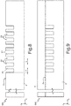
- Figure 7B shows, in top plan view in the plane XY, the portion of the photolithographic mask 60 including the openings 60'.
- the openings 60' have, by way of example, a quadrangular shape, for example a square shape with side l B comprised between 0.5 ⁇ m and 3 ⁇ m, and form an array of openings in which each opening 60' is arranged at a distance l D from an immediately adjacent opening comprised between 0.5 ⁇ m and 3 ⁇ m.
- openings 60' may have a shape and/or spatial arrangement different from the one illustrated in Figure 7B (for example, they may be circular or generically polygonal).
- an etching step is carried out, for example dry RIE, for selective removal of portions of the substrate 2 exposed through the openings 60' of the mask 60.
- etching portions of the semiconductor substrate 2 not protected by the mask 60 are removed, and etching proceeds until a desired depth, for example comprised between 0.5 ⁇ m and 5 ⁇ m, is reached (depth along Z measured starting from the surface 2a).
- Trenches 62 are thus formed in the substrate 2.
- each trench 62 has a square shape, in top plan view in the plane XY, with side a of a value substantially defined by the openings 60' of the etch mask 60, comprised between 0.5 ⁇ m and 3 ⁇ m, and a depth, measured along Z starting from the surface 2a of the substrate 2, of a value comprised between 0.5 ⁇ m and 5 ⁇ m.
- Each trench 62 is separated from another adjacent trench 62, along X, by walls or columns 64 of a thickness c comprised between 0.5 ⁇ m and 3 ⁇ m.
- the trenches 62 that, in subsequent steps, will concur in formation of a buried cavity are provided exclusively in the substrate 2.
- the buried cavity 18 will be formed substantially in the substrate 2.
- an epitaxial growth is carried out in deoxidizing environment (typically, in an atmosphere having a high hydrogen concentration, preferably using trichlorosilane - SiHCl 3 ). Consequently, an epitaxial layer 6, here having the first conductivity, grows on the silicon columns 64 and closes the trenches 62 at the top, trapping in the trenches 62 the gas present in the epitaxial-growth reactor (here, hydrogen molecules - H 2 ).
- the thickness of the epitaxial layer 6 is made of some microns, for example between 0.5 ⁇ m and 3 ⁇ m.
- An annealing step is then carried out, for example for 30 min at 1190°C.
- the annealing step causes ( Figure 10 ) migration of the silicon atoms, which tend to move into the position of lower energy, in a per se known manner, as, for example, discussed in the paper by T. Sato, N. Aoki, I. Mizushima and Y. Tsunashima, "A New Substrate Engineering for the Formation of Empty Space in Silicon (ESS) Induced by Silicon Surface Migration", IEDM 1999, pp. 517-520 .
- the silicon atoms migrate completely and form the buried cavity 18, closed at the top by the epitaxial layer 6.
- the previous annealing step is carried out in H 2 atmosphere so as to prevent the hydrogen present in the trenches 62 from escaping through the epitaxial layer 6 outwards and so as to increase the concentration of hydrogen present in the buried cavity 18 in the case where the hydrogen trapped during the step of epitaxial growth were not sufficient.
- annealing may be carried out in a nitrogen environment.
- Formation of a buried cavity 18 may likewise be carried out according to other processes of a known type, for example, as described in the scientific paper by Tsutomu Sato, et al., "Fabrication of Silicon-on-Nothing Structure by Substrate Engineering Using the Empty-Space-in-Silicon Formation Technique", Japanese Journal of Applied Physics, Vol. 43, No. 1, 2004, pp. 12-18 .
- the method described in the aforementioned scientific paper by Tsutomu Sato, et al. specify some parameters useful for setting the depth at which the buried cavity is formed.
- the buried cavity 18 may likewise be formed according to the process described in the paper by S. Armbruster et al., "A novel micromachining process for the fabrication of monocrystalline Si-membranes using porous silicon", TRANSDUCERS'03, The 12th International Conference on Solid State Sensors, Actuators and Microsystems, Boston, June 8-12 2003, Vol. 1, pp. 246-249 .
- process steps in themselves known, are then carried out as illustrated in Figure 11 , for the formation of one or more electronic components integrated in the epitaxial layer 6, which form the aforementioned electronic circuit 8.
- the electronic circuit 8 is created at portions of the epitaxial layer 6 that extend above the buried cavity 18.
- the steps of formation of the electronic circuit 8 may include steps of deposition of semiconductor material, implantations of dopant species, lithographic and etching steps, etc.
- etch mask 66 having openings 66' corresponding to regions where the trenches 25 that reach the buried cavity 18, thus arranging it in communication with the external environment, are to be formed.
- the etch mask 66 protects, in this step and in the subsequent steps, the underlying electronic circuit 8.
- the openings 66' of the etch mask 66 extend, in view in the plane XY, so as to implement one of the embodiments of Figures 3A-3C , or another embodiment provided by the present disclosure. In view in the plane XZ, the openings 66' extend, along Z, above the cavity 18.
- the size of the openings 66' may be selected so that the aspect ratio of the trenches 62 (ratio between the depth of the trenches 62 and their maximum width) is equal to 2 or higher than 2, for example comprised between 2 and 50.
- the trenches 25 are provided by wet or dry etching of the wafer 300 (represented schematically, in Figure 12 , by arrows 49), for selective removal of exposed portions of the epitaxial layer 6, until the buried cavity 18 is reached.
- the trenches 25 are formed in peripheral regions of the buried cavity 18, at a sufficient distance from the electronic circuit 8 so as not to jeopardise operation or structural integrity thereof.
- the epitaxial layer 6 (here of monocrystalline silicon) may be removed by an etching chemistry with a base of sulphur hexafluoride (SF 6 ) and octafluorocyclobutane (C 4 F 8 ). Other etching chemistries may be used, according to the need.
- the etch mask 66 may then be removed from the wafer 300.
- a step of at least partial filling of the buried cavity 18 is carried out to provide a plate 20 of the capacitor 1 and the dielectric 21, according to one of the embodiments of Figures 1 , 2 , and 4 .
- a similar procedure is carried out to provide the capacitor 40 of Figure 5 .
- the wafer 300 is arranged in a deposition reactor, in particular a reactor configured to carry out atomic-layer deposition (ALD), and ALD of dielectric material, for example Al 2 O 3 , TiO 2 , GeO 2 , Si 3 N 4 , La 2 O 3 , is carried out to form the dielectric layer 21 described previously.
- ALD atomic-layer deposition
- the ALD technique enables a uniform deposition of the dielectric inside the cavity 18 and along the walls of the trenches 25.
- the deposition parameters envisage a temperature comprised between 100°C and 500°C.
- the dielectric layer 21 by a step of thermal growth of silicon oxide.
- a step is carried out of deposition, for example by CVD, of polysilicon (in this example, with a doping of an N type) or of metal material such as tungsten (W) or titanium (Ti) or copper (Cu), to form the buried conductive region 20.
- CVD chemical vapor deposition
- metal material such as tungsten (W) or titanium (Ti) or copper (Cu)
- the conductive material chosen penetrates into the trenches 25 and deposits on the side walls, top wall, and bottom wall of the buried cavity 18, to form a filling layer that coats the inner walls of the buried cavity 18 completely.
- the conductive material coats the walls of the trenches 25, to form an electrical path in contact with the buried conductive region in the cavity 18.
- the process of deposition of conductive material continues until the trenches 25 are completely filled.
- the dielectric layer 21 has likewise the function of protective barrier against diffusion of conductive species (in particular metal) of the buried conductive region 20 within the substrate 2 and the epitaxial layer 6.
- respective dielectric and conductive layers are formed on the top surface 6a of the epitaxial layer 6.
- a subsequent step of photolithographic definition of said layers at the top surface 6a of the epitaxial layer 6 enables formation of the conductive paths 28 and of the underlying dielectric layer 29 of Figures 1-4 .
- the step previously described of deposition of the buried conductive region 20 by CVD may be replaced, or integrated, with a step of deposition by ALD technique, which may be used for covering more complex geometries, such as possible corners of the buried cavity and/or for deposition of metal materials with high conductivity (aluminium, copper, etc.).
- the pre-metal dielectric (PMD) layer 22 is formed, for example by depositing silicon oxide, on the front of the wafer 300, i.e., on the epitaxial layer 6 and on the conductive paths 28.
- the pre-metal dielectric layer 22 is selectively removed, by known lithographic and etching steps, to form one or more trenches 71 (just one of which is illustrated in the figure), which, once filled with conductive material, form the respective electrical paths 10 previously described for electrical contact of specific portions of the electronic circuit 8.
- one or more further trenches 72 are formed, which, once filled with conductive material, will form the conductive trenches 32 of Figures 1-4 .
- the conductive trench 36 of Figure 4 may simultaneously be formed.
- Filling of the trenches 71 and 72 is carried out, for example, by CVD, depositing metal material, in particular tungsten, aluminium, or copper.
- the back contact 34 is formed according to the embodiments of Figures 1 and 2 .
- the steps for the production of the capacitor 40 of Figure 5 are similar to those described previously, with the appropriate variants for filling of the buried cavity 18.
- a series of steps of thermal oxidation and/or CVD/ALD are carried out to form in succession the insulating region 42, the first conductive region 44, the dielectric 46, and the second conductive region 48.
- the steps described with reference to Figures 13 and 14 are carried out.
- the manufacturing process described envisages formation of a buried cavity in a monolithic semiconductor body, without the need to carry out bonding operations.
- the structural stability is thus improved, and the manufacturing costs are reduced.
- the semiconductor body 2 which would otherwise have an exclusive function of structural support, is exploited actively.
- the value of density of capacitance per unit area of the embedded capacitor according to the various embodiments of the present invention is high, in particular higher than the typical value of MIM capacitors (e.g., approximately twice, i.e., 10000 pF/mm 2 ).
- the first conductivity may be of an N type
- the second conductivity may be of a P type
- the electronic circuit 8 may not be present, or may be formed in an area of the die 100 different from the one illustrated in the figures, for example laterally staggered, in top plan view, with respect to the cavity 18.
Abstract
Description
- The present disclosure relates to a semiconductor die with buried capacitor, and to a method of manufacturing the semiconductor die.
- Capacitors are components of primary importance in integrated circuits. In order to meet different requirements of circuit applications, various types of capacitors have been proposed, each with characteristics of their own. On account of the limited capacitance per unit area, capacitors generally occupy a considerable area within the integrated circuit to which they belong. Selecting a type of capacitor over another is thus a fundamental aspect in the design of integrated circuits.
- Known in the art are basically three types of capacitors, namely, metal-oxide-semiconductor (MOS) capacitors, metal-insulating-metal (MIM) capacitors, and metal-oxide-metal (MOM) capacitors. Of these, owing to their thin gate-oxide structure, MOS capacitors have the highest value of density of capacitance per unit area. However, they suffer from considerable disadvantages, such as an accentuated not-linearity, a high temperature coefficient, and a low breakdown voltage, which render them not suitable for all circuit applications. MIM and MOM capacitors overcome the disadvantages of MOS capacitors; however, the densities of capacitance of said MIM and MOM capacitors are considerably lower as compared to MOS capacitors. Consequently, the use of MIM and MOM capacitors entails a higher consumption of area.
- As a consequence of what has been discussed above, in many applications it is preferable to use discrete capacitors external to the integrated circuit (e.g., SMD capacitors).
- There is thus felt the need for capacitors that enable the critical aspects of capacitors of a known type to be overcome and at the same time enable a saving of area.
- The aim of the present invention is thus to provide a semiconductor die with buried capacitor, and a method of manufacturing the semiconductor die that are alternative to those of the prior art and that enable the drawbacks of the prior art to be overcome.
- According to the present invention, a semiconductor die with buried capacitor and a method of manufacturing the semiconductor die are provided, as defined in the annexed claims.
- For a better understanding of the present invention, preferred embodiments thereof are now described, purely by way of non-limiting example, with reference to the attached drawings, wherein:
-
Figure 1 shows, in lateral sectional view, a semiconductor die with buried capacitor, according to one embodiment of the present invention; -
Figure 2 shows, in lateral sectional view, a semiconductor die with buried capacitor, according to a further embodiment of the present invention alternative to that ofFigure 1 ; -
Figures 3A-3C show, in top plan view, the semiconductor die ofFigure 1 according to respective layouts; -
Figures 4 and5 show, in lateral sectional view, respective semiconductor dice with buried capacitor, according to respective further embodiments of the present invention; and -
Figures 6-14 show a wafer during manufacturing steps for the production of the semiconductor die ofFigure 1 . -
Figure 1 is a schematic lateral sectional view, in a triaxial system X, Y, Z, of a portion of a die, or chip, 100 that houses an integrated semiconductor device, in particular including acapacitor 1, according to one aspect of the present invention. The view ofFigure 1 is a cross-sectional view taken along the line of section I-I ofFigures 3A-3C . Thecapacitor 1 is of an integrated type, or embedded, in the die 100. - The die 100 comprises a
semiconductor substrate 2, made, for example, of silicon, having a first conductivity (e.g., of a P type) and having atop surface 2a opposite, along Z, to abottom surface 2b. By way of example, thesemiconductor substrate 2 is doped with a concentration of P dopant species comprised between 1015 and 1018 at./cm3. In the context of the present invention, the die 100 may likewise be provided, on thetop surface 2a of thesubstrate 2, with one or moreepitaxial layers 6, which are also of semiconductor material, for example silicon, and have the first conductivity, for an overall thickness, along Z, for example comprised between 10 µm and 100 µm. - The die 100 further comprises a buried
conductive region 20 extending in the substrate 2 (and possibly, in part, in the epitaxial layer 6), of doped polysilicon or of metal material or a metal alloy. Examples of materials that may be used include, but not are limited to, Ru, Pt, Ir, Pd, Ag, Au, W, Cu, Co, Fe, Ni, Mo, Ta, Ti, Al, doped Si, doped Ge, etc. - According to the embodiment illustrated in
Figure 1 , the buriedconductive region 20 is electrically insulated fromsubstrate 2, and from theepitaxial layer 6, by a layer ofdielectric material 21, made, for example, of silicon oxide. According to one aspect of the present invention, the layer ofdielectric material 21 is made of a material with high dielectric constant k (known in the art as "high-k material"). Materials that may be used include, but not are limited to, Al2O3, TiO2, GeO2, Si3N4, La2O3, etc. - In an embodiment provided by way of example of the present invention, the buried
cavity 18 has, in top plan view in the plane XY, a shape chosen from among circular, oval, quadrangular, or generically polygonal, with a diameter comprised approximately between 10 µm and 1 mm and a base area comprised between 10 µm2 and 1 mm2. Alternatively, in a way not illustrated in the figure, it is likewise possible to form a plurality of membranes adjacent to one another, to form a suspended surface with total base area (sum of the areas of the adjacent membranes) of several square millimetres, according to the need. The extension he of the buriedcavity 18 in the direction Z is comprised approximately between 2 µm and 10 µm. The layer ofdielectric material 21 has a substantially uniform thickness hI; for example, it may be an atomic monolayer or may be formed by thousands of atomic monolayers arranged on top of one another. The buriedconductive region 20 has, in top plan view in the plane XY, a shape and size defined by the buriedcavity 18 and by the layer ofdielectric material 21. - The buried
conductive region 20 is formed, according to one aspect of the present disclosure, in a buriedcavity 18 in thesemiconductor substrate 2. The walls of the buriedcavity 18 are completely covered by the dielectric 21, and extending over thedielectric layer 21, inside the buriedcavity 18, is the buriedconductive region 20. The buriedconductive region 20 may fill the buriedcavity 18 completely and uniformly (Figure 1 ) or else only partially (Figure 2 ), to define ahollow region 23 inside the buriedconductive region 20 that is completely surrounded by the buriedconductive region 20. The embodiment ofFigure 1 enables a better dissipation of heat as compared to the embodiment ofFigure 2 . - The presence or otherwise of one or more cavities internal to the buried
conductive region 20 may likewise depend upon the filling method used. - The buried
conductive region 20 is connected to the top surface of theepitaxial layer 6a by one or moreelectrical paths 24, which have a main extension along Z. Theelectrical paths 24 are provided intrenches 25 that extend starting from the buriedconductive region 20, through part of thesemiconductor substrate 2 and through the entire thickness of theepitaxial layer 6, towards thetop surface 6a of theepitaxial layer 6. Theelectrical paths 24 are made of conductive material, for example polysilicon or metal, in particular of the same material as the one used for forming the buried conductive region 20 (as will be described more fully in what follows; according to one embodiment, they may be formed simultaneously with the buried conductive region 20) . - Further an insulating layer, formed as prolongation of the dielectric 21, extends on the inner walls of the
trenches 25 to insulate theelectrical paths 24 electrically from thesubstrate 2 and from theepitaxial layer 6. In the embodiment ofFigures 1 and2 , as described in greater detail in what follows, the insulating layers internal to thetrenches 25 are made in the same manufacturing step as the dielectric 21 and are consequently identified by the same reference number. - In order to prevent any possible undesired contamination of the
epitaxial layer 6 and of thesubstrate 2 by the filling metal material of the buriedcavity 18 and of thetrenches 25, it is possible to carry out, prior to the step of formation of the dielectric 21, a step of formation of a barrier layer (not illustrated in the figures) designed to prevent diffusion of metal ions within theepitaxial layer 6 and thesubstrate 2. - The
electrical paths 24 are electrically connected toconductive paths 28, which extend on thetop surface 6a of theepitaxial layer 6. Theconductive paths 28 are further electrically insulated from theepitaxial layer 6 by interposition of a dielectric orinsulating layer 29. In an embodiment, thedielectric layer 29 extends on thetop surface 6a as a prolongation of the dielectric 21, whereas theconductive paths 28 extend on thedielectric layer 29 as a prolongation of the buriedconductive region 20. - The die 100 further comprises a pre-metal dielectric (PMD)
layer 22 made, for example, of silicon oxide, which extends over thetop surface 6a of theepitaxial layer 6. - The pre-metal
dielectric layer 22 may, for example, be made of silicon oxide and have a thickness chosen according to the need, for example comprised approximately between 0.5 µm and 3 µm. - For electrical access to one or more
conductive paths 28, one or moreconductive trenches 32 extend through the pre-metaldielectric layer 22, until the one or moreconductive paths 28 are electrically contacted. - Extending on a
bottom surface 2b of thesubstrate 2, opposite to thetop surface 2a of thesubstrate 2, is a back electrical-contact region 34, made, for example, of conductive material, such as a metal. - In use, the buried
conductive region 20 has the function of first plate of thecapacitor 1, which may be biased at a working voltage Vp by theconductive trench 32, theconductive path 28 coupled thereto, and the correspondingelectrical path 24. Thesubstrate 2 forms a second plate of thecapacitor 1, which may be biased at a respective working voltage by the backelectrical contact 34. In the example ofFigures 1 and2 , the working voltage applied on the backelectrical contact 34 is the ground voltage GND. - The dielectric 21 that extends between the buried
conductive region 20 and thesubstrate 2 forms a dielectric of thecapacitor 1 arranged between the first and second plates. -
Capacitor 1 is therefore a planar capacitor whose plates lie on a respective plane parallel to the XY plane, i.e. parallel to the plane of main extension ofsubstrate 2. In other words, the first plate of the capacitor, the second plate of the capacitor and the dielectric interposed are arranged one above the other (overlapped) along the Z-axis which is orthogonal to the top andbottom surfaces substrate 2, and to thetop surface 6a ofepitaxial layer 6. - According to an aspect of the present invention, the
epitaxial layer 6 houses, in a region 6', one or more electronic components, in particular designed and coupled to one another to form anelectronic circuit 8. The region 6' is a region that extends over the cavity 18 (i.e., the region 6' and thecavity 18 are superimposed on one another in top plan view). The electronic components that form theelectronic circuit 8 may include active components such as transistors (e.g., MOS transistors, DMOS transistors, VDMOS transistors, trench-MOS transistors, bipolar transistors, etc.), or else passive components such as resistors and/or diodes, or in general any other electronic component. Electrical-connection paths 10 (only one of which is illustrated in the figures) form respective electrical paths for supplying/picking up electrical signals to/from theelectronic circuit 8. The region that houses theelectronic circuit 8 is an active region of thedie 100, in which phenomena of transport and conduction of electric charge take place. Due to the configuration ofcapacitor 1 of planar type, the space devoted to house theelectronic cuircuit 8 is maximized and optimized. -
Figures 3A-3C illustrate in top plan view in the plane XY, limitedly to the elements of interest, respective layouts of thedie 100 ofFigures 1 and2 . - With reference to
Figure 3A , a plurality oftrenches 25 are present (here, two, but the number may be any), coupled to respectiveconductive paths 28, each of which is adapted to provide a point of electrical access for biasing the buriedconductive region 20. The region 6' that houses theelectronic circuit 8 extends, in this example, between thetrenches 25. - With reference to
Figure 3B , asingle trench 25, which is U-shaped, is present. Likewise, aconductive path 28 extends in a position corresponding to thetrench 25 and substantially follows the shape thereof in plan view, as does theconductive trench 32. This embodiment presents the advantage of providing a greater area of electrical contact for biasing the buriedconductive region 20, consequently reducing the series resistance. The region 6' that houses theelectronic circuit 8 is, in this example, partially surrounded by thetrench 25. - In an embodiment not illustrated, two
U-shaped trenches 25 may be present, which are specular to one another with respect to an axis parallel to the direction X. - In a further embodiment, which is not shown either, there may be present one or more trenches that have a substantially rectangular shape, with a main extension along the axis X and/or along the axis Y.
-
Figure 3C illustrates a further embodiment in which a plurality oftrenches 25 are present, which partially surround theelectronic circuit 8. -
Figure 4 shows thedie 100 in a further embodiment. Here, the backelectrical contact 34 is not present, and a conductive via 36 extends through the pre-metaldielectric layer 22 until theepitaxial layer 6, and via the latter thesubstrate 2, is reached and electrically contacted at itstop surface 6a, at a distance from theconductive paths 28. In a way similar to what has been described previously, the buriedconductive region 20 forms a first plate of thecapacitor 1, the dielectric 21 forms a dielectric arranged between the plates of thecapacitor 1, and thesubstrate 2 forms a second plate of thecapacitor 1. -
Figure 5 is a schematic lateral-sectional view, in the triaxial system X, Y, Z, of a portion of adie 200, in particular integrating acapacitor 40, according to a further embodiment of the present invention. - In a way similar to what has been described with reference to
Figures 1 and2 (the same reference numbers identify elements that are in common) thedie 200 comprises asemiconductor substrate 2 extending on which is anepitaxial layer 6, both being, for example, of an N type; likewise extending in thesubstrate 2 is a buriedcavity 18. Extending in the buriedcavity 18, and in particular on the internal wall of the buriedcavity 18, is aninsulating region 42, made, for example, of silicon oxide. - Extending on the insulating
region 42, inside the buriedcavity 18, is a firstconductive region 44, made, for example, of doped polysilicon, or else of metal or a metal alloy. Examples of materials that may be used include, but are not limited to, Ru, Pt, Ir, Pd, Ag, Au, W, Cu, Co, Fe, Ni, Mo, Ta, Ti, Al, doped Si, doped Ge, etc. The firstconductive region 44 is completely insulated from thesubstrate 2 by the insulatingregion 42. - Extending on the first
conductive region 44, in the buriedcavity 18, is adielectric region 46, in particular a dielectric with a high dielectric constant k (known in the art as "high-k material"). Materials that may be used include, but not are limited to, Al2O3, TiO2, GeO2, Si3N4, La2O3, etc. SiO2 may alternatively be used. - Finally, extending on the
dielectric region 46 is a secondconductive region 48, made, for example, of doped polysilicon, metal, or a metal alloy. The materials referred to previously for the firstconductive region 44 may be used also in this case. The secondconductive region 48 is completely insulated from the firstconductive region 44 by thedielectric region 46. In other words, thedielectric region 46 is arranged between the first and secondconductive regions - In the embodiment of
Figure 5 , the secondconductive region 48 delimits within it ahollow portion 50. In a different embodiment (not illustrated), the secondconductive region 48 may fill thehollow portion 50 completely, the latter thus not being present. - The first and second
conductive regions electrical paths trenches 55 formed through theepitaxial layer 6 and in part through thesemiconductor substrate 2. The first and secondelectrical paths conductive regions region 42 extends through thetrenches 55, in contact with the inner walls of thetrenches 55, between thesubstrate 2/epitaxial layer 6 and the firstelectrical path 50, so as to insulate electrically the firstelectrical contact 50 from thesubstrate 2/epitaxial layer 6. Likewise, also thedielectric region 46 extends through thetrenches 55, between the firstelectrical path 50 and the secondelectrical path 52, for electrically insulating the firstelectrical path 50 from the secondelectrical path 52. In this way, the first and secondconductive regions - In order to prevent any possible undesired contamination of the
epitaxial layer 6 and of thesubstrate 2 by the filling metal material of the buriedcavity 18 and of thetrenches 55, it is possible to carry out, prior to the step of formation of the insulatingregion 42, a step of formation of a barrier layer (not illustrated in the figures) designed to prevent diffusion of metal ions within theepitaxial layer 6 and thesubstrate 2. - The first and second
electrical paths conductive paths epitaxial layer 6, insulated from the latter by an insulatinglayer 58, which extends as a prolongation of the portion of the insulatingregion 42 inside the trenches 55 (this is, according to one aspect of the present invention, a single layer formed in a same manufacturing step; according to an alternative aspect, the insulatinglayer 58 could be formed in a different manufacturing step). - The die 200 further comprises a pre-metal dielectric (PMD)
layer 59, made, for example, of silicon oxide, which extends on thetop surface 6a of theepitaxial layer 6, coating the first and secondconductive paths - The pre-metal
dielectric layer 22 may, for example, be made of silicon oxide and have a thickness chosen according to the need, for example comprised between 0.5 µm and 3 µm. - Finally, first and second
conductive trenches dielectric layer 22 until they electrically contact the first and secondconductive paths - In a way similar to what has been described with reference to
Figures 1-4 , according to one aspect of the present invention, theepitaxial layer 6 houses, in a region 6', one or more electronic components, in particular designed and coupled to one another to form anelectronic circuit 8. The region 6' is a region that extends over the cavity 18 (i.e., the region 6' and thecavity 18 are superimposed on one another in top plan view). The electronic components that form theelectronic circuit 8 may include active components such as transistors (e.g., MOS transistors, DMOS transistors, VDMOS transistors, trench-MOS transistors, bipolar transistors, etc.), or else passive components such as resistors and/or diodes, or in general any other electronic component. Electrical-connection paths 10 (just one of which is illustrated in the figures) form respective electrical paths for supplying/picking up electrical signals to/from theelectronic circuit 8. The region that houses theelectronic circuit 8 is an active region of thedie 100, occurring in which are phenomena of transport and conduction of electric charge. - In use, the first
conductive region 44 has the function of first plate of thecapacitor 40, which may be biased at a working voltage V1 by the firstconductive trench 60, the firstconductive path 54 coupled thereto, and the firstelectrical contact 50. The secondconductive region 48 has the function of second plate of thecapacitor 40, which may be biased at a respective working voltage V2 by the secondconductive trench 62, the secondconductive path 56 coupled thereto, and the secondelectrical contact 52. Thedielectric region 46 arranged between the first and secondconductive regions -
Figures 6-14 show, in the same lateral sectional view as that ofFigure 1 , steps of processing of asemiconductor wafer 300 that lead to formation of thedie 100. - With reference to
Figure 6 , thesemiconductor substrate 2 made, for example, of doped silicon, is provided as described previously. - Then (
Figures 7A-10 ), steps of formation of the buried cavity (designated by thereference number 18 inFigure 9 ) are carried out, for example according to the method of creation of buried cavities described inUS 8,173,513 , filed in the name of the present applicant. - For this purpose (
Figure 7A ), anetch mask 60 is formed on thesurface 2a of thesubstrate 2, made, for example, of silicon oxide. Alternatively, the mask may be a photolithographic mask, of photoresist. Themask 60 is defined so as to provide a plurality of openings 60' in the region where the buriedcavity 18 is to be formed. -
Figure 7B shows, in top plan view in the plane XY, the portion of thephotolithographic mask 60 including the openings 60'. In this example, the openings 60' have, by way of example, a quadrangular shape, for example a square shape with side lB comprised between 0.5 µm and 3 µm, and form an array of openings in which each opening 60' is arranged at a distance lD from an immediately adjacent opening comprised between 0.5 µm and 3 µm. - It is, however, evident that the openings 60' may have a shape and/or spatial arrangement different from the one illustrated in
Figure 7B (for example, they may be circular or generically polygonal). - Next (
Figure 8 ), an etching step is carried out, for example dry RIE, for selective removal of portions of thesubstrate 2 exposed through the openings 60' of themask 60. During etching, portions of thesemiconductor substrate 2 not protected by themask 60 are removed, and etching proceeds until a desired depth, for example comprised between 0.5 µm and 5 µm, is reached (depth along Z measured starting from thesurface 2a). - Then, the
etch mask 60 is removed.Trenches 62 are thus formed in thesubstrate 2. - In one embodiment, each
trench 62 has a square shape, in top plan view in the plane XY, with side a of a value substantially defined by the openings 60' of theetch mask 60, comprised between 0.5 µm and 3 µm, and a depth, measured along Z starting from thesurface 2a of thesubstrate 2, of a value comprised between 0.5 µm and 5 µm. Eachtrench 62 is separated from anotheradjacent trench 62, along X, by walls orcolumns 64 of a thickness c comprised between 0.5 µm and 3 µm. - According to what is described with reference to
Figures 7A-8 , thetrenches 62 that, in subsequent steps, will concur in formation of a buried cavity, are provided exclusively in thesubstrate 2. In this case, also the buriedcavity 18 will be formed substantially in thesubstrate 2. In the case where the buried cavity were to be formed at a height, along Z, greater than the thickness of thesubstrate 2, it is possible to carry out, prior to the step ofFigure 7A , an epitaxial growth (in a way not illustrated in the figure). - With reference to
Figure 9 , an epitaxial growth is carried out in deoxidizing environment (typically, in an atmosphere having a high hydrogen concentration, preferably using trichlorosilane - SiHCl3). Consequently, anepitaxial layer 6, here having the first conductivity, grows on thesilicon columns 64 and closes thetrenches 62 at the top, trapping in thetrenches 62 the gas present in the epitaxial-growth reactor (here, hydrogen molecules - H2). The thickness of theepitaxial layer 6 is made of some microns, for example between 0.5 µm and 3 µm. - An annealing step is then carried out, for example for 30 min at 1190°C. The annealing step causes (
Figure 10 ) migration of the silicon atoms, which tend to move into the position of lower energy, in a per se known manner, as, for example, discussed in the paper by T. Sato, N. Aoki, I. Mizushima and Y. Tsunashima, "A New Substrate Engineering for the Formation of Empty Space in Silicon (ESS) Induced by Silicon Surface Migration", IEDM 1999, pp. 517-520. - Consequently, in the area of the
trenches 62 where thesilicon columns 64 are close to one another, the silicon atoms migrate completely and form the buriedcavity 18, closed at the top by theepitaxial layer 6. Preferably, the previous annealing step is carried out in H2 atmosphere so as to prevent the hydrogen present in thetrenches 62 from escaping through theepitaxial layer 6 outwards and so as to increase the concentration of hydrogen present in the buriedcavity 18 in the case where the hydrogen trapped during the step of epitaxial growth were not sufficient. Alternatively, annealing may be carried out in a nitrogen environment. - Formation of a buried
cavity 18 may likewise be carried out according to other processes of a known type, for example, as described in the scientific paper by Tsutomu Sato, et al., "Fabrication of Silicon-on-Nothing Structure by Substrate Engineering Using the Empty-Space-in-Silicon Formation Technique", Japanese Journal of Applied Physics, Vol. 43, No. 1, 2004, pp. 12-18. The method described in the aforementioned scientific paper by Tsutomu Sato, et al. specify some parameters useful for setting the depth at which the buried cavity is formed. - According to a further embodiment, the buried
cavity 18 may likewise be formed according to the process described in the paper by S. Armbruster et al., "A novel micromachining process for the fabrication of monocrystalline Si-membranes using porous silicon", TRANSDUCERS'03, The 12th International Conference on Solid State Sensors, Actuators and Microsystems, Boston, June 8-12 2003, Vol. 1, pp. 246-249. - Irrespective of the embodiment chosen for the formation of the buried
cavity 18, process steps, in themselves known, are then carried out as illustrated inFigure 11 , for the formation of one or more electronic components integrated in theepitaxial layer 6, which form the aforementionedelectronic circuit 8. Theelectronic circuit 8 is created at portions of theepitaxial layer 6 that extend above the buriedcavity 18. The steps of formation of theelectronic circuit 8 may include steps of deposition of semiconductor material, implantations of dopant species, lithographic and etching steps, etc. - Then (
Figure 12 ), a step is carried out of formation and photolithographic definition of anetch mask 66, having openings 66' corresponding to regions where thetrenches 25 that reach the buriedcavity 18, thus arranging it in communication with the external environment, are to be formed. Theetch mask 66 protects, in this step and in the subsequent steps, the underlyingelectronic circuit 8. - By way of example, the openings 66' of the
etch mask 66 extend, in view in the plane XY, so as to implement one of the embodiments ofFigures 3A-3C , or another embodiment provided by the present disclosure. In view in the plane XZ, the openings 66' extend, along Z, above thecavity 18. - Further, according to a further aspect of the present disclosure, the size of the openings 66' may be selected so that the aspect ratio of the trenches 62 (ratio between the depth of the
trenches 62 and their maximum width) is equal to 2 or higher than 2, for example comprised between 2 and 50. - In detail, the
trenches 25 are provided by wet or dry etching of the wafer 300 (represented schematically, inFigure 12 , by arrows 49), for selective removal of exposed portions of theepitaxial layer 6, until the buriedcavity 18 is reached. Thetrenches 25 are formed in peripheral regions of the buriedcavity 18, at a sufficient distance from theelectronic circuit 8 so as not to jeopardise operation or structural integrity thereof. The epitaxial layer 6 (here of monocrystalline silicon) may be removed by an etching chemistry with a base of sulphur hexafluoride (SF6) and octafluorocyclobutane (C4F8). Other etching chemistries may be used, according to the need. - The
etch mask 66 may then be removed from thewafer 300. - Next (
Figure 13 ), a step of at least partial filling of the buriedcavity 18 is carried out to provide aplate 20 of thecapacitor 1 and the dielectric 21, according to one of the embodiments ofFigures 1 ,2 , and4 . A similar procedure is carried out to provide thecapacitor 40 ofFigure 5 . - For this purpose, according to one aspect of the present disclosure, the
wafer 300 is arranged in a deposition reactor, in particular a reactor configured to carry out atomic-layer deposition (ALD), and ALD of dielectric material, for example Al2O3, TiO2, GeO2, Si3N4, La2O3, is carried out to form thedielectric layer 21 described previously. The ALD technique enables a uniform deposition of the dielectric inside thecavity 18 and along the walls of thetrenches 25. The deposition parameters envisage a temperature comprised between 100°C and 500°C. - As an alternative to the ALD step, it is possible to form the
dielectric layer 21 by a step of thermal growth of silicon oxide. - Then, a step is carried out of deposition, for example by CVD, of polysilicon (in this example, with a doping of an N type) or of metal material such as tungsten (W) or titanium (Ti) or copper (Cu), to form the buried
conductive region 20. By adjusting the deposition parameters, in particular by selecting a temperature comprised between 100°C and 500°C, the present applicant has found that the conductive material chosen penetrates into thetrenches 25 and deposits on the side walls, top wall, and bottom wall of the buriedcavity 18, to form a filling layer that coats the inner walls of the buriedcavity 18 completely. At the same time, the conductive material coats the walls of thetrenches 25, to form an electrical path in contact with the buried conductive region in thecavity 18. The process of deposition of conductive material continues until thetrenches 25 are completely filled. - The
dielectric layer 21 has likewise the function of protective barrier against diffusion of conductive species (in particular metal) of the buriedconductive region 20 within thesubstrate 2 and theepitaxial layer 6. - With the previous steps, respective dielectric and conductive layers are formed on the
top surface 6a of theepitaxial layer 6. A subsequent step of photolithographic definition of said layers at thetop surface 6a of theepitaxial layer 6 enables formation of theconductive paths 28 and of theunderlying dielectric layer 29 ofFigures 1-4 . - The step previously described of deposition of the buried
conductive region 20 by CVD may be replaced, or integrated, with a step of deposition by ALD technique, which may be used for covering more complex geometries, such as possible corners of the buried cavity and/or for deposition of metal materials with high conductivity (aluminium, copper, etc.). - Next (
Figure 14 ), the pre-metal dielectric (PMD)layer 22 is formed, for example by depositing silicon oxide, on the front of thewafer 300, i.e., on theepitaxial layer 6 and on theconductive paths 28. The pre-metaldielectric layer 22 is selectively removed, by known lithographic and etching steps, to form one or more trenches 71 (just one of which is illustrated in the figure), which, once filled with conductive material, form the respectiveelectrical paths 10 previously described for electrical contact of specific portions of theelectronic circuit 8. Simultaneously, one or morefurther trenches 72 are formed, which, once filled with conductive material, will form theconductive trenches 32 ofFigures 1-4 . Likewise, in this step, also theconductive trench 36 ofFigure 4 may simultaneously be formed. - Filling of the
trenches - Likewise, the
back contact 34 is formed according to the embodiments ofFigures 1 and2 . - The steps for the production of the
capacitor 40 ofFigure 5 are similar to those described previously, with the appropriate variants for filling of the buriedcavity 18. In detail, after the step ofFigure 12 , a series of steps of thermal oxidation and/or CVD/ALD are carried out to form in succession the insulatingregion 42, the firstconductive region 44, the dielectric 46, and the secondconductive region 48. Then, the steps described with reference toFigures 13 and14 are carried out. - From what has been described above, the advantages of the invention illustrated, in the various embodiments, are evident.
- For instance, the manufacturing process described envisages formation of a buried cavity in a monolithic semiconductor body, without the need to carry out bonding operations. The structural stability is thus improved, and the manufacturing costs are reduced. Further, the
semiconductor body 2, which would otherwise have an exclusive function of structural support, is exploited actively. - Further, the value of density of capacitance per unit area of the embedded capacitor according to the various embodiments of the present invention is high, in particular higher than the typical value of MIM capacitors (e.g., approximately twice, i.e., 10000 pF/mm2).
- Finally, it is evident that modifications and variations may be made to the invention described, without departing from the scope of the present disclosure, as defined in the annexed claims.
- For instance, the first conductivity may be of an N type, and the second conductivity may be of a P type.
- Further, the
electronic circuit 8 may not be present, or may be formed in an area of thedie 100 different from the one illustrated in the figures, for example laterally staggered, in top plan view, with respect to thecavity 18.
Claims (19)
- A semiconductor die (100; 200) comprising:- a semiconductor body (2, 6), having a front side (6a) and a back side (2b), housing an electronic circuit (8);- a buried region (18) in the semiconductor body (2, 6) between the electronic circuit (8) and the back side (2b), including a first layer of conductive material (20; 48) and a dielectric layer (21; 46) arranged between the first layer of conductive material (20; 48) and the semiconductor body (2, 6); and- at least a first conductive path (24, 25; 50, 52, 55) between the buried region (18) and the front side (6a), which forms a path for electrical access to the first layer of conductive material (20),wherein said first laye3r of conductive material (20; 48) forms a first plate of a capacitor (1; 40) buried in the semiconductor body (2, 6), and the dielectric layer (21; 46) forms a dielectric of said capacitor (1; 40).
- The die (100) according to claim 1, wherein said semiconductor body (2, 6) forms a second plate of said capacitor (1), the dielectric layer (21) being the dielectric arranged between the first and second plates of said capacitor (1).
- The die (200) according to claim 1, wherein the buried region (18) further comprises a second layer of conductive material (44), between the dielectric layer (46) and the semiconductor body (2, 6), which forms a second plate of said capacitor (1), the dielectric layer (46) being the dielectric arranged between the first and second plates of said capacitor (1).
- The die (200) according to claim 3, further comprising an insulating layer (42) arranged between the second layer of conductive material (44) and the semiconductor body (2, 6), configured to electrically insulate the second layer of conductive material (44) from the semiconductor body (2, 6).
- The die (200) according to claim 3 or claim 4, comprising at least one second conductive path (50, 52, 55) between the buried region (18) and the front side (6a), which forms a path for electrical access to the second layer of conductive material (44).
- The die (100; 200) according to any one of the preceding claims, further comprising a pre-metal dielectric layer (22) on the front side (6a) of the semiconductor body (2, 6), and at least one first front contact (32; 62), which extends through the pre-metal dielectric layer (22) until the first conductive path (24, 25; 50, 52, 55) is electrically contacted and is configured to bias, in use, the first layer of conductive material (20; 48) at a first operating voltage (VP; V2).
- The die (200) according to claim 6 when depending upon claim 5, further comprising at least one second front contact (60), which extends through the pre-metal dielectric layer (22) until the second conductive path (50, 54) is electrically contacted and is configured to bias, in use, the second layer of conductive material (44) at a second operating voltage (V1).
- The die (100) according to claim 5, further comprising a back contact (34), which extends on the back side (2b) of the semiconductor body (2, 6) and is configured to bias, in use, the semiconductor body (2, 6) at an operating reference voltage (GND).
- The die (100) according to claim 5, further comprising a second front contact (36), which extends through the pre-metal dielectric layer (22) until the semiconductor body (2, 6) is reached and electrically contacted and is configured to bias, in use, the semiconductor body (2, 6) at an operating reference voltage (GND).
- The die (100; 200) according to any one of the preceding claims, wherein the first layer of conductive material (20; 48) and the first conductive path (24, 25; 50, 52, 55) are made of a same material and form a continuous path.
- The die (100; 200) according to any one of the preceding claims, wherein the first layer of conductive material (20; 48) is made of a material chosen between doped polysilicon, metal, or a metal alloy.
- The die (100; 200) according to any one of the preceding claims, wherein said semiconductor body (2, 6) includes:a substrate (2) having a first conductivity type; andan epitaxial layer (6), having the first conductivity type, which extends over the substrate (2),wherein the buried region (18) extends in the substrate (2), and the electronic circuit extends in the epitaxial layer (6).
- A method of manufacturing a semiconductor die (100; 200) comprising the steps of:- forming, in a semiconductor body (2, 6) having a front side (6a) and a back side (2b), a buried region (18) including a first layer of conductive material (20; 48) and a dielectric layer (21; 46) arranged between the first layer of conductive material (20; 48) and the semiconductor body (2, 6);- forming, in the semiconductor body (2, 6) between the buried region (18) and the front side (6a), an electronic circuit (8); and- forming a path for electrical access to the first layer of conductive material (20) to form at least one first conductive path (24, 25; 50, 52, 55) between the buried region (18) and the front side (6a),wherein said first layer of conductive material (20; 48) is designed to operate as first plate of a capacitor (1; 40) buried in the semiconductor body (2, 6), and the dielectric layer (21; 46) is designed to operate as dielectric of said capacitor (1; 40).
- The method of manufacturing a semiconductor die (100; 200) according to claim 13, wherein said semiconductor body (2, 6) is designed to operate as a second plate of said capacitor (1), the dielectric layer (21) being the dielectric arranged between the first and second plates of said capacitor (1).
- The method of manufacturing a semiconductor die (200) according to claim 13, wherein the step of forming the buried region (18) further comprises forming a second layer of conductive material (44) between the dielectric layer (46) and the semiconductor body (2, 6), designed to operate as a second plate of said capacitor (1).
- The method of manufacturing a semiconductor die (200) according to claim 15, further comprising the step of forming an insulating layer (42) between the second layer of conductive material (44) and the semiconductor body (2, 6), configured to electrically insulate the second layer of conductive material (44) from the semiconductor body (2, 6).
- The method of manufacturing a semiconductor die (100; 200) according to any one of claims 13-16, wherein the step of forming the buried region (18) comprises the steps of:- forming a buried cavity (18) in the semiconductor body (2, 6);- etching selective portions of the semiconductor body until the buried cavity (18) is reached to form one or more openings (66') for fluidic access to the buried cavity (18);- depositing dielectric material within the buried cavity (18) through the one or more openings (66') so as to coat completely the inner walls of the buried cavity to form the dielectric layer (21; 46); and- depositing conductive material within the buried cavity (18) through the one or more openings (66') so as to coat the dielectric layer (21; 46) completely, thus forming the first layer of conductive material (20; 48).
- The method of manufacturing a semiconductor die (200) according to any one of claims 13-16, wherein the step of forming the buried region (18) comprises the steps of:- forming a buried cavity (18) in the semiconductor body (2, 6);- etching selective portions of the semiconductor body until the buried cavity (18) is reached to form one or more openings (66') for fluidic access to the buried cavity (18);- forming an insulating layer (42) within the buried cavity (18) by deposition or thermal growth so as to coat the inner walls of the buried cavity completely;- depositing conductive material within the buried cavity (18) through the one or more openings (66') so as to coat the insulating layer (42) completely, thus forming a second layer of conductive material (44);- depositing a layer of dielectric material within the buried cavity (18) so as to cover the second layer of conductive material (44) completely, thus forming the dielectric layer (46); and- depositing conductive material within the buried cavity (18) through the one or more openings (66') in order to coat the dielectric layer (46) completely, thus forming the first layer of conductive material (44).
- The method of manufacturing a semiconductor die (100; 200) according to claim 17 or claim 18, wherein the steps of depositing dielectric material and conductive material include carrying out respective depositions with CVD and/or ALD technology.
Applications Claiming Priority (1)
| Application Number | Priority Date | Filing Date | Title |
|---|---|---|---|
| IT201800000947A IT201800000947A1 (en) | 2018-01-15 | 2018-01-15 | SEMICONDUCTOR PLATE WITH BURIED CONDENSER, AND MANUFACTURING METHOD OF THE SEMICONDUCTOR PLATE |
Publications (1)
| Publication Number | Publication Date |
|---|---|
| EP3511975A1 true EP3511975A1 (en) | 2019-07-17 |
Family
ID=61802338
Family Applications (1)
| Application Number | Title | Priority Date | Filing Date |
|---|---|---|---|
| EP19151970.1A Pending EP3511975A1 (en) | 2018-01-15 | 2019-01-15 | Semiconductor die with buried capacitor, and method of manufacturing the semiconductor die |
Country Status (4)
| Country | Link |
|---|---|
| US (2) | US10930799B2 (en) |
| EP (1) | EP3511975A1 (en) |
| CN (2) | CN110047817B (en) |
| IT (1) | IT201800000947A1 (en) |
Families Citing this family (5)
| Publication number | Priority date | Publication date | Assignee | Title |
|---|---|---|---|---|
| US10141303B1 (en) * | 2017-09-20 | 2018-11-27 | Cree, Inc. | RF amplifier package with biasing strip |
| IT201800000947A1 (en) * | 2018-01-15 | 2019-07-15 | St Microelectronics Srl | SEMICONDUCTOR PLATE WITH BURIED CONDENSER, AND MANUFACTURING METHOD OF THE SEMICONDUCTOR PLATE |
| EP3849286A1 (en) * | 2020-01-09 | 2021-07-14 | Murata Manufacturing Co., Ltd. | Electronic device with differential transmission lines equipped with 3d capacitors supported by a base, and corresponding manufacturing method |
| US11532592B2 (en) | 2020-05-08 | 2022-12-20 | Western Digital Technologies, Inc. | Capacitor die for stacked integrated circuits |
| CN113990932A (en) * | 2021-10-28 | 2022-01-28 | 电子科技大学 | Semiconductor longitudinal device and preparation method |
Citations (5)
| Publication number | Priority date | Publication date | Assignee | Title |
|---|---|---|---|---|
| US20080048231A1 (en) * | 2006-08-28 | 2008-02-28 | Micron Technology, Inc. | Buried decoupling capacitors, devices and systems including same, and methods of fabrication |
| US20090176347A1 (en) * | 2008-01-04 | 2009-07-09 | International Business Machines Corporation | Hybrid orientation substrate compatible deep trench capacitor embedded dram |
| US8173513B2 (en) | 2004-03-19 | 2012-05-08 | Stmicroelectronics S.R.L. | Method for manufacturing a semiconductor pressure sensor |
| US20170221901A1 (en) * | 2013-09-25 | 2017-08-03 | Intel Corporation | Methods of forming buried vertical capacitors and structures formed thereby |
| US20170250253A1 (en) * | 2016-02-25 | 2017-08-31 | Stmicroelectronics S.R.L. | Semiconductor device with buried conductive region, and method for manufacturing the semiconductor device |
Family Cites Families (15)
| Publication number | Priority date | Publication date | Assignee | Title |
|---|---|---|---|---|
| EP0847089B1 (en) * | 1996-12-09 | 2002-10-23 | STMicroelectronics S.r.l. | Method and device for suppressing parasitic effects in a junction-insulated integrated circuit |
| US6437385B1 (en) * | 2000-06-29 | 2002-08-20 | International Business Machines Corporation | Integrated circuit capacitor |
| KR100442781B1 (en) * | 2001-12-24 | 2004-08-04 | 동부전자 주식회사 | semiconductor having having trench capacitor and method for fabricating the same |
| EP1480266A3 (en) * | 2003-05-20 | 2006-03-15 | STMicroelectronics S.A. | Process of making integrated electronic circuit with stacked elements and corresponding integrated electronic circuit. |
| US7276787B2 (en) * | 2003-12-05 | 2007-10-02 | International Business Machines Corporation | Silicon chip carrier with conductive through-vias and method for fabricating same |
| JP2005203615A (en) * | 2004-01-16 | 2005-07-28 | Sony Corp | Semiconductor memory, semiconductor device and manufacturing methods for these |
| US7465642B2 (en) * | 2005-10-28 | 2008-12-16 | International Business Machines Corporation | Methods for forming semiconductor structures with buried isolation collars |
| US7439127B2 (en) * | 2006-04-20 | 2008-10-21 | Advanced Micro Devices, Inc. | Method for fabricating a semiconductor component including a high capacitance per unit area capacitor |
| EP2147499B1 (en) * | 2007-05-10 | 2016-08-17 | Nxp B.V. | Dc-to-dc converter comprising a reconfigurable capacitor unit |
| US7923815B2 (en) * | 2008-01-07 | 2011-04-12 | International Business Machines Corporation | DRAM having deep trench capacitors with lightly doped buried plates |
| US8188528B2 (en) * | 2009-05-07 | 2012-05-29 | International Buiness Machines Corporation | Structure and method to form EDRAM on SOI substrate |
| JP2012182336A (en) * | 2011-03-02 | 2012-09-20 | Toshiba Corp | Semiconductor device |
| CN102412193A (en) * | 2011-06-08 | 2012-04-11 | 上海华虹Nec电子有限公司 | Through silicon via (TSV) filling method |
| US9620582B2 (en) * | 2015-01-27 | 2017-04-11 | Taiwan Semiconductor Manufacturing Co., Ltd. | Metal-insulator-metal (MIM) capacitors and forming methods |
| IT201800000947A1 (en) * | 2018-01-15 | 2019-07-15 | St Microelectronics Srl | SEMICONDUCTOR PLATE WITH BURIED CONDENSER, AND MANUFACTURING METHOD OF THE SEMICONDUCTOR PLATE |
-
2018
- 2018-01-15 IT IT201800000947A patent/IT201800000947A1/en unknown
-
2019
- 2019-01-14 CN CN201910033479.1A patent/CN110047817B/en active Active
- 2019-01-14 US US16/246,945 patent/US10930799B2/en active Active
- 2019-01-14 CN CN201920056837.6U patent/CN209461454U/en active Active
- 2019-01-15 EP EP19151970.1A patent/EP3511975A1/en active Pending
-
2021
- 2021-01-20 US US17/153,599 patent/US20210143286A1/en not_active Abandoned
Patent Citations (5)
| Publication number | Priority date | Publication date | Assignee | Title |
|---|---|---|---|---|
| US8173513B2 (en) | 2004-03-19 | 2012-05-08 | Stmicroelectronics S.R.L. | Method for manufacturing a semiconductor pressure sensor |
| US20080048231A1 (en) * | 2006-08-28 | 2008-02-28 | Micron Technology, Inc. | Buried decoupling capacitors, devices and systems including same, and methods of fabrication |
| US20090176347A1 (en) * | 2008-01-04 | 2009-07-09 | International Business Machines Corporation | Hybrid orientation substrate compatible deep trench capacitor embedded dram |
| US20170221901A1 (en) * | 2013-09-25 | 2017-08-03 | Intel Corporation | Methods of forming buried vertical capacitors and structures formed thereby |
| US20170250253A1 (en) * | 2016-02-25 | 2017-08-31 | Stmicroelectronics S.R.L. | Semiconductor device with buried conductive region, and method for manufacturing the semiconductor device |
Non-Patent Citations (5)
| Title |
|---|
| "EMBEDDED MEMORY: THE ALL-PURPOSE CORE", EDN ELECTRICAL DESIGN NEWS.(TEXAS INSTRUMENT), REED BUSINESS INFORMATION, HIGHLANDS RANCH, CO, US, vol. 43, no. 6, 13 March 1998 (1998-03-13), pages 34, XP000869377, ISSN: 0012-7515 * |
| LU N C C ET AL: "A BURIED-TRENCH DRAM CELL USING A SELF-ALIGNED EPITAXY OVER TRENCH TECHNOLOGY", INTERNATIONAL ELECTRON DEVICES MEETING. SAN FRANCISCO, DEC. 11 - 14, 1988; [INTERNATIONAL ELECTRON DEVICES MEETING], NEW YORK, IEEE, US, vol. -, 1 January 1988 (1988-01-01), pages 588 - 591, XP001008457 * |
| S. ARMBRUSTER ET AL.: "A novel micromachining process for the fabrication of monocrystalline Si-membranes using porous silicon", TRANSDUCERS'03, THE 12TH INTERNATIONAL CONFERENCE ON SOLID STATE SENSORS, ACTUATORS AND MICROSYSTEMS, vol. 1, 8 June 2003 (2003-06-08), pages 246 - 249, XP010646515 |
| T. SATO; N. AOKI; I. MIZUSHIMA; Y. TSUNASHIMA: "A New Substrate Engineering for the Formation of Empty Space in Silicon (ESS) Induced by Silicon Surface Migration", IEDM, 1999, pages 517 - 520, XP010372210, DOI: doi:10.1109/IEDM.1999.824206 |
| TSUTOMU SATO ET AL.: "Fabrication of Silicon-on-Nothing Structure by Substrate Engineering Using the Empty-Space-in-Silicon Formation Technique", JAPANESE JOURNAL OF APPLIED PHYSICS, vol. 43, no. 1, 2004, pages 12 - 18, XP001191452, DOI: doi:10.1143/JJAP.43.12 |
Also Published As
| Publication number | Publication date |
|---|---|
| CN209461454U (en) | 2019-10-01 |
| US20190221678A1 (en) | 2019-07-18 |
| CN110047817A (en) | 2019-07-23 |
| US10930799B2 (en) | 2021-02-23 |
| IT201800000947A1 (en) | 2019-07-15 |
| CN110047817B (en) | 2024-03-19 |
| US20210143286A1 (en) | 2021-05-13 |
Similar Documents
| Publication | Publication Date | Title |
|---|---|---|
| US10930799B2 (en) | Semiconductor die with buried capacitor, and method of manufacturing the semiconductor die | |
| US10692966B2 (en) | Deep trench capacitor with scallop profile | |
| TW202010045A (en) | Film scheme for a high density trench capacitor | |
| US7786014B2 (en) | Electronic device and method for making the same | |
| US10170497B2 (en) | Method for manufacturing an electronic device and method for operating an electronic device | |
| US10062757B2 (en) | Semiconductor device with buried metallic region, and method for manufacturing the semiconductor device | |
| US9917009B2 (en) | Methods of forming a through-substrate-via (TSV) and a metallization layer after formation of a semiconductor device | |
| US20130175666A1 (en) | Semiconductor device having capacitor integrated therein | |
| TWI690024B (en) | Semiconductor device and method of manufacturing the same | |
| CN111092047B (en) | Semiconductor device and method for manufacturing the same | |
| CN106960847A (en) | Storage arrangement and its manufacture method | |
| US10319805B2 (en) | Method of fabricating semiconductor devices | |
| US11374000B2 (en) | Trench capacitor with lateral protrusion structure | |
| CN111211032B (en) | Method for manufacturing semiconductor structure and plasma processing equipment | |
| CN105826361B (en) | Semiconductor devices and its manufacturing method | |
| CN115346924A (en) | Semiconductor device and method for manufacturing the same | |
| CN113130746A (en) | Semiconductor structure and forming method thereof | |
| CN104555897A (en) | Method for electrochemically producing at least one porous region of a micro- and/or nanoelectronic structure | |
| US20240047383A1 (en) | Semiconductor structure having deep trench capacitor and method of manufacturing thereof | |
| US20230068854A1 (en) | Method of making a plurality of 3d semiconductor devices with enhanced mobility and conductivity | |
| US11869949B2 (en) | Semiconductor device and manufacturing method thereof | |
| WO2022266995A1 (en) | Multi-layer polysilicon stack for semiconductor devices | |
| CN113345896A (en) | Dynamic random access memory device and manufacturing method thereof | |
| CN117460246A (en) | Method for manufacturing semiconductor structure and semiconductor structure |
Legal Events
| Date | Code | Title | Description |
|---|---|---|---|
| PUAI | Public reference made under article 153(3) epc to a published international application that has entered the european phase |
Free format text: ORIGINAL CODE: 0009012 |
|
| STAA | Information on the status of an ep patent application or granted ep patent |
Free format text: STATUS: THE APPLICATION HAS BEEN PUBLISHED |
|
| AK | Designated contracting states |
Kind code of ref document: A1 Designated state(s): AL AT BE BG CH CY CZ DE DK EE ES FI FR GB GR HR HU IE IS IT LI LT LU LV MC MK MT NL NO PL PT RO RS SE SI SK SM TR |
|
| AX | Request for extension of the european patent |
Extension state: BA ME |
|
| STAA | Information on the status of an ep patent application or granted ep patent |
Free format text: STATUS: REQUEST FOR EXAMINATION WAS MADE |
|
| 17P | Request for examination filed |
Effective date: 20191220 |
|
| RBV | Designated contracting states (corrected) |
Designated state(s): AL AT BE BG CH CY CZ DE DK EE ES FI FR GB GR HR HU IE IS IT LI LT LU LV MC MK MT NL NO PL PT RO RS SE SI SK SM TR |
|
| STAA | Information on the status of an ep patent application or granted ep patent |
Free format text: STATUS: EXAMINATION IS IN PROGRESS |
|
| 17Q | First examination report despatched |
Effective date: 20200518 |
|
| STAA | Information on the status of an ep patent application or granted ep patent |
Free format text: STATUS: EXAMINATION IS IN PROGRESS |