EP3511807A1 - Display device and flexible circuit board - Google Patents
Display device and flexible circuit board Download PDFInfo
- Publication number
- EP3511807A1 EP3511807A1 EP19150455.4A EP19150455A EP3511807A1 EP 3511807 A1 EP3511807 A1 EP 3511807A1 EP 19150455 A EP19150455 A EP 19150455A EP 3511807 A1 EP3511807 A1 EP 3511807A1
- Authority
- EP
- European Patent Office
- Prior art keywords
- display
- display device
- touch
- substrate
- circuit board
- Prior art date
- Legal status (The legal status is an assumption and is not a legal conclusion. Google has not performed a legal analysis and makes no representation as to the accuracy of the status listed.)
- Granted
Links
Images









Classifications
-
- G—PHYSICS
- G06—COMPUTING OR CALCULATING; COUNTING
- G06F—ELECTRIC DIGITAL DATA PROCESSING
- G06F3/00—Input arrangements for transferring data to be processed into a form capable of being handled by the computer; Output arrangements for transferring data from processing unit to output unit, e.g. interface arrangements
- G06F3/01—Input arrangements or combined input and output arrangements for interaction between user and computer
- G06F3/03—Arrangements for converting the position or the displacement of a member into a coded form
- G06F3/041—Digitisers, e.g. for touch screens or touch pads, characterised by the transducing means
- G06F3/0416—Control or interface arrangements specially adapted for digitisers
- G06F3/04164—Connections between sensors and controllers, e.g. routing lines between electrodes and connection pads
-
- H—ELECTRICITY
- H10—SEMICONDUCTOR DEVICES; ELECTRIC SOLID-STATE DEVICES NOT OTHERWISE PROVIDED FOR
- H10K—ORGANIC ELECTRIC SOLID-STATE DEVICES
- H10K59/00—Integrated devices, or assemblies of multiple devices, comprising at least one organic light-emitting element covered by group H10K50/00
- H10K59/40—OLEDs integrated with touch screens
-
- G—PHYSICS
- G06—COMPUTING OR CALCULATING; COUNTING
- G06F—ELECTRIC DIGITAL DATA PROCESSING
- G06F3/00—Input arrangements for transferring data to be processed into a form capable of being handled by the computer; Output arrangements for transferring data from processing unit to output unit, e.g. interface arrangements
- G06F3/01—Input arrangements or combined input and output arrangements for interaction between user and computer
- G06F3/03—Arrangements for converting the position or the displacement of a member into a coded form
- G06F3/041—Digitisers, e.g. for touch screens or touch pads, characterised by the transducing means
-
- G—PHYSICS
- G06—COMPUTING OR CALCULATING; COUNTING
- G06F—ELECTRIC DIGITAL DATA PROCESSING
- G06F3/00—Input arrangements for transferring data to be processed into a form capable of being handled by the computer; Output arrangements for transferring data from processing unit to output unit, e.g. interface arrangements
- G06F3/01—Input arrangements or combined input and output arrangements for interaction between user and computer
- G06F3/03—Arrangements for converting the position or the displacement of a member into a coded form
- G06F3/041—Digitisers, e.g. for touch screens or touch pads, characterised by the transducing means
- G06F3/0412—Digitisers structurally integrated in a display
-
- G—PHYSICS
- G06—COMPUTING OR CALCULATING; COUNTING
- G06F—ELECTRIC DIGITAL DATA PROCESSING
- G06F3/00—Input arrangements for transferring data to be processed into a form capable of being handled by the computer; Output arrangements for transferring data from processing unit to output unit, e.g. interface arrangements
- G06F3/01—Input arrangements or combined input and output arrangements for interaction between user and computer
- G06F3/03—Arrangements for converting the position or the displacement of a member into a coded form
- G06F3/041—Digitisers, e.g. for touch screens or touch pads, characterised by the transducing means
- G06F3/044—Digitisers, e.g. for touch screens or touch pads, characterised by the transducing means by capacitive means
-
- G—PHYSICS
- G09—EDUCATION; CRYPTOGRAPHY; DISPLAY; ADVERTISING; SEALS
- G09F—DISPLAYING; ADVERTISING; SIGNS; LABELS OR NAME-PLATES; SEALS
- G09F9/00—Indicating arrangements for variable information in which the information is built-up on a support by selection or combination of individual elements
- G09F9/30—Indicating arrangements for variable information in which the information is built-up on a support by selection or combination of individual elements in which the desired character or characters are formed by combining individual elements
- G09F9/301—Indicating arrangements for variable information in which the information is built-up on a support by selection or combination of individual elements in which the desired character or characters are formed by combining individual elements flexible foldable or roll-able electronic displays, e.g. thin LCD, OLED
-
- H—ELECTRICITY
- H05—ELECTRIC TECHNIQUES NOT OTHERWISE PROVIDED FOR
- H05K—PRINTED CIRCUITS; CASINGS OR CONSTRUCTIONAL DETAILS OF ELECTRIC APPARATUS; MANUFACTURE OF ASSEMBLAGES OF ELECTRICAL COMPONENTS
- H05K1/00—Printed circuits
- H05K1/02—Details
- H05K1/0277—Bendability or stretchability details
- H05K1/028—Bending or folding regions of flexible printed circuits
-
- H—ELECTRICITY
- H05—ELECTRIC TECHNIQUES NOT OTHERWISE PROVIDED FOR
- H05K—PRINTED CIRCUITS; CASINGS OR CONSTRUCTIONAL DETAILS OF ELECTRIC APPARATUS; MANUFACTURE OF ASSEMBLAGES OF ELECTRICAL COMPONENTS
- H05K1/00—Printed circuits
- H05K1/18—Printed circuits structurally associated with non-printed electric components
- H05K1/189—Printed circuits structurally associated with non-printed electric components characterised by the use of flexible or folded printed circuits
-
- H—ELECTRICITY
- H05—ELECTRIC TECHNIQUES NOT OTHERWISE PROVIDED FOR
- H05K—PRINTED CIRCUITS; CASINGS OR CONSTRUCTIONAL DETAILS OF ELECTRIC APPARATUS; MANUFACTURE OF ASSEMBLAGES OF ELECTRICAL COMPONENTS
- H05K3/00—Apparatus or processes for manufacturing printed circuits
- H05K3/36—Assembling printed circuits with other printed circuits
- H05K3/361—Assembling flexible printed circuits with other printed circuits
-
- H—ELECTRICITY
- H10—SEMICONDUCTOR DEVICES; ELECTRIC SOLID-STATE DEVICES NOT OTHERWISE PROVIDED FOR
- H10K—ORGANIC ELECTRIC SOLID-STATE DEVICES
- H10K50/00—Organic light-emitting devices
- H10K50/80—Constructional details
- H10K50/84—Passivation; Containers; Encapsulations
- H10K50/844—Encapsulations
-
- H—ELECTRICITY
- H10—SEMICONDUCTOR DEVICES; ELECTRIC SOLID-STATE DEVICES NOT OTHERWISE PROVIDED FOR
- H10K—ORGANIC ELECTRIC SOLID-STATE DEVICES
- H10K50/00—Organic light-emitting devices
- H10K50/80—Constructional details
- H10K50/86—Arrangements for improving contrast, e.g. preventing reflection of ambient light
- H10K50/865—Arrangements for improving contrast, e.g. preventing reflection of ambient light comprising light absorbing layers, e.g. light-blocking layers
-
- H—ELECTRICITY
- H10—SEMICONDUCTOR DEVICES; ELECTRIC SOLID-STATE DEVICES NOT OTHERWISE PROVIDED FOR
- H10K—ORGANIC ELECTRIC SOLID-STATE DEVICES
- H10K59/00—Integrated devices, or assemblies of multiple devices, comprising at least one organic light-emitting element covered by group H10K50/00
- H10K59/10—OLED displays
- H10K59/12—Active-matrix OLED [AMOLED] displays
- H10K59/122—Pixel-defining structures or layers, e.g. banks
-
- H—ELECTRICITY
- H10—SEMICONDUCTOR DEVICES; ELECTRIC SOLID-STATE DEVICES NOT OTHERWISE PROVIDED FOR
- H10K—ORGANIC ELECTRIC SOLID-STATE DEVICES
- H10K59/00—Integrated devices, or assemblies of multiple devices, comprising at least one organic light-emitting element covered by group H10K50/00
- H10K59/10—OLED displays
- H10K59/12—Active-matrix OLED [AMOLED] displays
- H10K59/131—Interconnections, e.g. wiring lines or terminals
-
- H—ELECTRICITY
- H10—SEMICONDUCTOR DEVICES; ELECTRIC SOLID-STATE DEVICES NOT OTHERWISE PROVIDED FOR
- H10K—ORGANIC ELECTRIC SOLID-STATE DEVICES
- H10K59/00—Integrated devices, or assemblies of multiple devices, comprising at least one organic light-emitting element covered by group H10K50/00
- H10K59/30—Devices specially adapted for multicolour light emission
- H10K59/38—Devices specially adapted for multicolour light emission comprising colour filters or colour changing media [CCM]
-
- H—ELECTRICITY
- H10—SEMICONDUCTOR DEVICES; ELECTRIC SOLID-STATE DEVICES NOT OTHERWISE PROVIDED FOR
- H10K—ORGANIC ELECTRIC SOLID-STATE DEVICES
- H10K71/00—Manufacture or treatment specially adapted for the organic devices covered by this subclass
-
- H—ELECTRICITY
- H10—SEMICONDUCTOR DEVICES; ELECTRIC SOLID-STATE DEVICES NOT OTHERWISE PROVIDED FOR
- H10K—ORGANIC ELECTRIC SOLID-STATE DEVICES
- H10K77/00—Constructional details of devices covered by this subclass and not covered by groups H10K10/80, H10K30/80, H10K50/80 or H10K59/80
- H10K77/10—Substrates, e.g. flexible substrates
- H10K77/111—Flexible substrates
-
- G—PHYSICS
- G06—COMPUTING OR CALCULATING; COUNTING
- G06F—ELECTRIC DIGITAL DATA PROCESSING
- G06F2203/00—Indexing scheme relating to G06F3/00 - G06F3/048
- G06F2203/041—Indexing scheme relating to G06F3/041 - G06F3/045
- G06F2203/04103—Manufacturing, i.e. details related to manufacturing processes specially suited for touch sensitive devices
-
- H—ELECTRICITY
- H05—ELECTRIC TECHNIQUES NOT OTHERWISE PROVIDED FOR
- H05K—PRINTED CIRCUITS; CASINGS OR CONSTRUCTIONAL DETAILS OF ELECTRIC APPARATUS; MANUFACTURE OF ASSEMBLAGES OF ELECTRICAL COMPONENTS
- H05K2201/00—Indexing scheme relating to printed circuits covered by H05K1/00
- H05K2201/10—Details of components or other objects attached to or integrated in a printed circuit board
- H05K2201/10007—Types of components
- H05K2201/10128—Display
-
- H—ELECTRICITY
- H10—SEMICONDUCTOR DEVICES; ELECTRIC SOLID-STATE DEVICES NOT OTHERWISE PROVIDED FOR
- H10K—ORGANIC ELECTRIC SOLID-STATE DEVICES
- H10K59/00—Integrated devices, or assemblies of multiple devices, comprising at least one organic light-emitting element covered by group H10K50/00
- H10K59/80—Constructional details
- H10K59/87—Passivation; Containers; Encapsulations
- H10K59/871—Self-supporting sealing arrangements
- H10K59/8722—Peripheral sealing arrangements, e.g. adhesives, sealants
-
- H—ELECTRICITY
- H10—SEMICONDUCTOR DEVICES; ELECTRIC SOLID-STATE DEVICES NOT OTHERWISE PROVIDED FOR
- H10K—ORGANIC ELECTRIC SOLID-STATE DEVICES
- H10K59/00—Integrated devices, or assemblies of multiple devices, comprising at least one organic light-emitting element covered by group H10K50/00
- H10K59/80—Constructional details
- H10K59/8791—Arrangements for improving contrast, e.g. preventing reflection of ambient light
-
- H—ELECTRICITY
- H10—SEMICONDUCTOR DEVICES; ELECTRIC SOLID-STATE DEVICES NOT OTHERWISE PROVIDED FOR
- H10K—ORGANIC ELECTRIC SOLID-STATE DEVICES
- H10K71/00—Manufacture or treatment specially adapted for the organic devices covered by this subclass
- H10K71/40—Thermal treatment, e.g. annealing in the presence of a solvent vapour
Definitions
- Exemplary embodiments of the invention relate to a display device and a flexible circuit board.
- a display device visually displays data.
- the display device generally includes a display panel for displaying an image and a window disposed outside the display panel to protect the display panel.
- a bonding layer is disposed between the display panel and the window to attach the display panel and the window to each other.
- the bonding layer is applied to the window in a liquid phase, and is cured by ultraviolet light after the display panel and the window are laminated.
- the display device may include a touch sensing function interacting with a user in addition to a function of displaying the image. That is, a recent display device may further include a touch sensing layer and a flexible circuit board coupled to the touch sensing layer as well as the display panel, the window, and the bonding layer.
- a transmission of ultraviolet (“UV”) light may be inhibited by the flexible circuit board around an area where the flexible circuit board is coupled to the touch sensing layer, and thus there is a possibility that a part of the bonding layer is not sufficiently cured, thereby deteriorating a reliability of the display device.
- UV ultraviolet
- Exemplary embodiments of the invention provide a display device having improved reliability.
- exemplary embodiments of the invention provide a flexible circuit board capable of manufacturing a display device having improved reliability.
- An exemplary embodiment may be related to a display device.
- the display device includes a display structure including a display panel and a touch sensing layer disposed on the display panel, the display panel including a display panel including a display area and a non-display area around the display area, and the touch sensing layer including a first portion overlapping the display area and a second portion overlapping the non-display area, a window structure disposed on the display structure, a bonding layer disposed between the display structure and the window structure, and a touch flexible circuit board electrically connected with the touch sensing layer, wherein the touch flexible circuit board includes a first substrate member connected to the second portion, and a second substrate member provided with an UV transmitting member transmitting UV light emitted from a side of the bonding layer and extending from the first substrate member in a predetermined direction.
- the ultraviolet transmitting member does not overlap the touch sensing layer, that is, the ultraviolet transmitting member is in a plan view onto the touch sensing layer positioned outside the touch sensing layer.
- the second substrate member includes a bending portion extending from the first substrate member and an extension portion extending from the bending portion and disposed under the display structure, and the ultraviolet transmitting member is defined at the bending portion.
- the bending portion does not overlap the touch sensing layer, that is, the bending portion is in a plan view onto the touch sensing layer positioned outside the touch sensing layer.
- An exemplary embodiment may be related to a display device.
- the display device includes a display structure, a window, which also might be called window element, disposed on the display structure, a light blocking member disposed on one surface of the window facing the display structure, a bonding layer between the window and the display structure, and a flexible circuit board including a first substrate member and a second substrate member provided with an UV transmitting member overlapping the light blocking member and extending from the first substrate member.
- An exemplary embodiment may be related to a flexible circuit board.
- the flexible circuit board includes a first substrate member connected with an electronic device, a second substrate member extending from the first substrate member and provided with an opening member, and an UV transmitting resin layer provided in the opening member.
- the opening member may be also called an opening structure, especially an opening pattern.
- first”, “second”, etc. may be used herein to describe various elements, these elements, should not be limited by these terms. These terms may be used to distinguish one element from another element. Thus, a first element discussed below may be termed a second element without departing from teachings of one or more embodiments. The description of an element as a “first” element may not require or imply the presence of a second element or other elements.
- the terms “first”, “second”, etc. may also be used herein to differentiate different categories or sets of elements. For conciseness, the terms “first”, “second”, etc. may represent “first-category (or first-set)", “second-category (or second-set)", etc., respectively.
- Exemplary embodiments are described herein with reference to cross section illustrations that are schematic illustrations of idealized embodiments. As such, variations from the shapes of the illustrations as a result, for example, of manufacturing techniques and/or tolerances, are to be expected. Thus, embodiments described herein should not be construed as limited to the particular shapes of regions as illustrated herein but are to include deviations in shapes that result, for example, from manufacturing. In an exemplary embodiment, a region illustrated or described as flat may, typically, have rough and/or nonlinear features. Moreover, sharp angles that are illustrated may be rounded. Thus, the regions illustrated in the figures are schematic in nature and their shapes are not intended to illustrate the precise shape of a region and are not intended to limit the scope of the claims.
- FIG. 1 is an exploded perspective view of a display device according to an exemplary embodiment
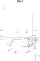
- FIG. 2 is a plan view of a display device according to an exemplary embodiment
- FIG. 3 is a plan view showing a state before bending of a touch flexible circuit board included in a display device according to an exemplary embodiment
- FIG. 4 is a cross-sectional view taken along line B1-B1' in FIG. 3
- FIG. 5 is a cross-sectional view of the display device of FIGS. 1 and 2 taken along line A-A' in FIGS. 1 and 2
- FIG. 6 is a cross-sectional view of the display device of FIGS. 1 and 2 taken along line B-B' in FIGS. 1 and 2
- FIG. 7 is a cross-sectional view of the display device of FIGS. 1 and 2 taken along line C-C' in FIGS. 1 and 2 .
- the line B1-B1' in FIG. 3 is a part of the line B-B' in FIGS. 1 and 2 .
- a display device 1 may include a display structure DS, a window structure 40 disposed over the display structure DS, a bonding layer 70 disposed between the window structure 40 and the display structure DS, and a touch flexible circuit board 50 connected to the display structure DS.
- the display device 1 may further include a panel flexible circuit board 60 and a display driver IC, which are connected to the display structure DS.
- the display device 1 may further include a panel protection member 80 disposed beneath the display structure DS.
- the display structure may include a display panel 10 and a touch sensing layer 20, and may further include an optical member 30.
- the display panel 10 may have a rectangular shape in a plan view.
- the display panel 10 may include both opposite long sides extending in the first direction x and both opposite short sides extending in the second direction y intersecting the first direction x.
- the corner where the long side and short side of the display panel 10 meet each other may have a right angle, but is not limited thereto, and may have a curved surface.
- the corner of the display panel 10 may also be chamfered to reduce the risk of breakage.
- the planar shape of the display panel 10 is not limited to the illustrated one, and may include various other shapes such as a circular shape.
- the display panel 10 includes a display area DA and a non-display area NDA in a plan view.
- the display area DA is an area where an image is displayed
- the non-display area NDA is an area where an image is not displayed.
- the non-display area NDA may be disposed around the display area DA, and may surround the display area DA.
- the terms “on”, “over”, “upper side”, “upper surface”, or “top” means a side facing an arrow in the third directions z intersecting the first direction x and the second direction y based on the drawings
- the terms “beneath”, “under”, “lower side”, “lower surface”, or “bottom” means a side opposite to the side facing the arrow in the third direction z based on the drawings.
- the display panel 10 includes a first substrate 11, a second substrate 12 disposed over the first substrate 11 and attached to the first substrate 11, and a display layer disposed between the first substrate 11 and the second substrate 12.
- the first substrate 11 is a substrate for supporting the display layer.
- the first substrate 11 may include a polymer film such as glass or plastic.
- the display layer is disposed on the first substrate 11 and is located in the display area DA.
- the display layer may include a plurality of pixels and a plurality of display signal lines.
- Each pixel may include a thin film transistor ("TFT"), a capacitor, and a light emitting element, which will be described later.
- the plurality of display signal lines may include a gate line to transmit a gate signal to each pixel and a data line to transmit a data signal to each pixel.
- the display signal line may extend to the non-display area NDA.
- the display driver IC may be disposed on the first substrate 11.
- the display driver IC may include at least one of a data driver for applying a data signal to a data line, a gate driver for applying a gate signal to a gate line, and a signal control member for controlling the operations of the data driver and the gate driver.
- the display driver IC may be electrically connected with the display layer through the display signal line extending to the non-display area NDA or a separate wiring.
- the display driver IC may be located adjacent to the short side of the first substrate 11 in the non-display area NDA.
- the display driver IC may be disposed (e.g., mounted) on the first substrate 11.
- the display driver IC may be disposed (e.g., mounted) on the first substrate 11 in the form of a chip on glass ("COG").
- COG chip on glass
- the display driver IC may also be disposed (e.g., mounted) on the first substrate 11 in the form of a chip on plastic ("COP").
- the invention is not limited thereto, and, in another exemplary embodiment, the display driver IC may be disposed on the panel flexible circuit board 60, or may be disposed on a separate main circuit board (not shown).
- a case where the display driver IC is disposed (e.g., mounted) on the first substrate 11 in the non-display area NDA will be described as an example.
- the second substrate 12 may be an encapsulation substrate for preventing moisture and/or oxygen from penetrating into the display member from the outside.
- the second substrate 12 may include a polymer film such as glass or plastic.
- the second substrate 12 may be smaller than the first substrate 11, and may cover the first substrate 11 and the display member in the display area DA.
- the second substrate 12 may be attached to the first substrate 11 by a sealant (not shown) applied along the edge of the second substrate 12 in the non-display area NDA.
- a thin film encapsulation layer in which at least one organic film and at least one inorganic film are alternately laminated one by one may be provided instead of the second substrate 12.
- the touch sensing layer 20 may be disposed on the display panel 10.
- the touch sensing layer 20 may obtain the coordinates of a touch input point in a capacitive manner.
- the coordinate information of the touched point may be obtained in a self capacitive manner or a mutual capacitive manner.
- the touch sensing layer 20 has a mutual capacitive structure will be described as an example, but the invention is not limited thereto.
- the touch sensing layer 20 may be disposed on the second substrate 12 of the display panel 10, and may include a first portion 21 overlapping the display area DA of the display panel 10 and a second portion 23 overlapping the non-display area NDA of the display panel 10.
- the first portion 21 of the touch sensing layer 20 may include a touch electrode (not shown), and the second portion 23 thereof may include a touch signal line (not shown) to transmit and/or receiving a signal to/from the touch electrode and a pad portion provided by the extension of the touch signal line.
- the touch electrode, touch signal line and pad portion of the touch sensing layer 20 may be disposed directly on the second substrate 12. In other words, a separate bonding layer (for example, an adhesive layer) may not be disposed between the touch sensing layer 20 and the second substrate 12.
- the optical member 30 may be disposed on the touch sensing layer 20.
- the optical member 30 may include at least one of a phase retardation member and a polarization member.
- the polarization member may be disposed on the phase retardation member.
- External light incident from the outside of the window structure 40 passes through the polarization member to be linearly polarized.
- the linearly polarized incident light passes through the phase retardation member, is reflected, is incident on the phase retardation member again, passes through the phase retardation member again and then is incident on the polarization member.
- the linearly polarized incident light passes through the phase retardation member to have a phase difference of about 45°, and is circularly polarized to change its phase.
- the phase retardation member again, most of the external light disappears without passing through the polarization member.
- right-turn circularly polarized light having passed through the phase retardation member is reflected and converted into left-turn circularly polarized light, and the right-turn circularly polarized light and the left-turn circularly polarized light may disappear by destructive interference, for example. Therefore, the external light reflectance of the display device 1 may decrease.
- the optical member 30 may be omitted.
- the optical member 30 may be disposed in the display panel 10 instead of being disposed on the touch sensing layer 20.
- the optical member 30 is disposed on the touch sensing layer 20 will be described as an example.
- the panel protection member 80 may be disposed under the display structure DS.
- the panel protection member 80 may include at least one of a buffer member and a heat radiation member.
- the buffer member may include a material having a high shock absorption rate.
- the buffer member may include a polymer resin, such as polyurethane, polycarbonate, polypropylene, or polyethylene, or may be a sponge obtained by foam-molding a rubber liquid, a urethane-based material or an acrylic material.
- the invention is not limited thereto.
- the heat radiation member may include at least one of graphite, copper (Cu), and aluminum (Al), having good heat radiation characteristics, for example, but is not limited thereto.
- the heat radiation member not only improves the heat radiation characteristics but also has electromagnetic wave blocking or electromagnetic wave absorbing characteristics.
- the panel protection member 80 may be attached to the display structure DS through an adhesive layer, a double-sided adhesive tape, or the like.
- the panel flexible circuit board 60 may be connected to the display panel 10 of the display structure DS.
- the panel flexible circuit board 60 is a component to which a signal for controlling the display driver IC or the display layer is applied, and the panel flexible circuit board 60 may be connected to the first substrate 11 in the non-display area NDA.
- the panel flexible circuit board 60 may include a first panel substrate member 610, a second panel substrate member 630, a connection member 650, and an input member 670.
- the first panel substrate member 610 is a portion of the panel flexible circuit substrate 60 connected to the first substrate 11 in the non-display area NDA.
- the first panel substrate member 610 may be connected to the pad portion (not shown) provided on the first substrate 11, and, in some exemplary embodiments, may be connected to the pad portion through an anisotropic conductive film or the like.
- the invention is not limited thereto, and the first panel substrate member 610 may be connected to the pad portion (not shown) provided on the first substrate 11 by an ultrasonic bonding method or the like, for example.
- the first panel substrate member 610 may be located at a portion adjacent to one short side of the first substrate 11 extending along the second direction y in the non-display area NDA.
- the second panel substrate member 630 which is a portion extending from the first panel substrate member 610, may extend along the first direction x from the first panel substrate member 610 and may be bent toward the lower side of the display structure DS or the lower side of the panel protection member 80. That is, a part of the second panel substrate member 630 may include a bent portion extending from the first panel substrate member 610 and a portion extending from the bent portion and located under the display structure DS or the panel protection member 80.
- connection member 650 may be disposed on the second panel substrate member 630, and, in some exemplary embodiments, may overlap the display structure DS or the panel protection member 80.
- the connection member 650 may be a portion connected to the touch flexible circuit board 50 to be described later.
- the connection member 650 may be provided in the form of a connector or the like.
- the connection member 650 when a connection member 570 included in the touch flexible circuit board 50 is provided in a form of a female connector, the connection member 650 may be provided in a form of a male connector, for example.
- the connection member 570 included in the touch flexible circuit board 50 is provided in the form of a male connector, the connection member 650 may be provided in the form of a female connector.
- the input member 670 is a portion receiving a signal from the outside, and, in some exemplary embodiments, may be connected to a main circuit board (not shown). In some exemplary embodiments, the input member 670 may be part of the second panel substrate member 630 or may be disposed on the second panel substrate member 630.
- the touch flexible circuit board 50 may be electrically connected to the touch sensing layer 20 of the display structure DS.
- the touch flexible circuit board 50 may include a first substrate member 510 and a second substrate member 530, and may further include a touch driver 550 and a connection member 570.
- the first substrate member 510 may be connected to the second portion 23 of the touch sensing layer 20, overlapping the non-display region NDA, and, in some exemplary embodiments, may be connected to the pad portion of the second portion 23 of the touch sensing layer 20. In some exemplary embodiments, the first substrate member 510 may be connected to the second portion 23 through an anisotropic conductive film or the like. However, the invention is not limited thereto, and the first substrate member 510 may be connected to the second portion 23 by various methods such as ultrasonic bonding. In some exemplary embodiments, the first substrate member 510 may be located at the same side as a portion of the display structure DS where the first panel substrate member 610 is disposed, but the invention is not limited thereto.
- the second substrate member 530 is a portion extending from the first substrate member 510 and not being connected to the touch sensing layer 20.
- the second substrate member 530 may be bent toward the lower side of the display structure DS or the lower side of the panel protection member 80. That is, the second substrate member 530 may include a bending portion 530A extending from the first substrate member 510 and an extension portion 530B extending from the bending portion 530A.
- the first substrate member 510 and the extension portion 530B may be provided in a substantially flat shape while the touch flexible circuit board 50 is bent, and the bending portion 530A may be provided in a bent shape.
- the bending portion 530A may extend along the first direction x from the first substrate member 510, and may not overlap the touch sensing layer 20 in the plan view. Further, the bending portion 530A may overlap a light blocking member 43 of the window structure 40, which will be described later. In some exemplary embodiments, the bending portion 530A may include a portion of which a width in the second direction y varies along the first direction x. In an exemplary embodiment, the bending portion 530A may include a portion of which a width in the second direction y decreases as the portion is farther from the first substrate member 510 along the first direction x, for example.
- the extension portion 530B may extend from the bending portion 530A and be located under the display structure DS or the panel protection member 80. In some exemplary embodiments, the extension portion 530B may overlap the second portion 23 of the touch sensing layer 20, and may further overlap the first portion 21 of the touch sensing layer 20 or the display area DA of the display panel 10.
- the touch driver 550 may transmit a touch driving signal to the touch sensing layer 20.
- the touch driver 550 may process a touch sensing signal received from the touch sensing layer 20 to generate touch information such as whether to touch and touch position.
- the touch driver 550 may be disposed (e.g., mounted) on the extension portion 530B.
- the second substrate member 530 may be provided with the connection member 570.
- the connection member 570 may be provided on the extension portion 530B of the second substrate member 530.
- the connection member 570 may be connected to the connection member 650 of the panel flexible circuit board 60.
- the touch flexible circuit board 50 may receive an external signal input through the input member 670 of the panel flexible circuit board 60 and/or a signal generated/processed by the circuit element of the panel flexible circuit board 60.
- the connection member 570 may be provided in the form of a connector, as described above.
- the second substrate member 530 may be provided with an ultraviolet ("UV") transmitting member.
- the UV transmitting member transmits UV light emitted from the side surface of the bonding layer 70 when curing bonding layer 70.
- the UV transmitting member may be composed of an opening member 59 defined in the second substrate member 530.
- the opening member 59 may be defined in a form of a hole penetrating the touch flexible circuit board 50, and may be defined in the bending portion 530A of the second substrate member 530. Since the bending portion 530A may overlap the light blocking member 43 of the window structure 40, the opening member 59 may also overlap the light blocking member 43. Further, since the bending portion 530A may not overlap the touch sensing layer 20, the opening member 59 may also not overlap the touch sensing layer 20.
- the opening member 59 may be also called an opening structure 59 or opening pattern 59.
- the opening member 59 may include one or more openings.
- the opening member 59 may include a first opening 591 and a second opening 593, and may further include a third opening 595 and a fourth opening 597, for example.
- the second opening 593 compared to the first opening 591, may be located adjacent to the edge of the bending portion 530A.
- the minimum distance along the second direction y between the second opening 593 and the edge of the bending portion 530A may be shorter than the minimum distance along the second direction y between the edge of the first opening 591 and the edge of the bending portion 530A.
- the planar shapes of the first opening 591 and the second opening 593 may be different from each other.
- the second opening 593 may have a triangular shape in which the width of the second opening 593 in the second direction decreases along the first direction x, for example.
- this is merely an example, and, in another exemplary embodiment, the first opening 591 and the second opening 593 may have the same shape.
- the third opening 595 may have a shape symmetrical to the first opening 591 with respect to an imaginary line extending along the first direction x
- the fourth opening 597 may have a shape symmetrical to the second opening 593 with respect to an imaginary line extending along the first direction x.
- the number of openings included in the opening member 59 may be variously changed.
- the number of openings included in the opening member 59 may be one, two, three, five or more, for example.
- the window structure 40 is disposed over the display structure DS to protect the display structure DS from external shocks and scratches.
- the window structure 40 may include a light transmitting area TA and a light blocking area BA in a plan view.
- the light transmitting area TA is an area through which light is transmitted, and an image provided from the display panel 10 may be transmitted to a user through the light transmitting area TA.
- the light blocking area BA may be an area for blocking light transmission.
- the light blocking area BA may be located around the light transmitting area TA, and may surround the light transmitting area TA.
- the light transmitting area TA may overlap the display area DA of the display panel 10 and may not overlap the non-display area NDA of the display panel 10.
- the light blocking area BA may overlap the non-display area NDA of the display panel 10 and may not overlap the display area DA of the display panel 10. That is, the light blocking area BA may cover the non-display area NDA of the display panel 10.
- the window structure 40 may include a window (or window element) 41 and a light blocking member 43.
- the light blocking member 43 may be disposed on one surface of the window 41 facing the display structure DS.
- the light blocking member 43 may define the light blocking area BA of the window structure 40.
- the light blocking member 43 may be a colored organic layer, and may be disposed on one side of the window 41 by coating, printing, or the like.
- the light blocking member 43 is disposed on a base layer such as a transparent film, and the base layer on which the light blocking member 43 is disposed may be attached to one side of the window 41.
- the bonding layer 70 may be disposed between the window structure 40 and the display structure DS to couple the window structure 40 with the display structure DS.
- the bonding layer 70 may be provided to fill the entire space between the light transmitting area TA of the window structure 40 and the display structure DS. In some exemplary embodiments, the bonding layer 70 may be provided to further fill a part of the space between the light blocking area BA of the window structure 40 and the display structure DS.
- the bonding layer 70 may include an UV-curable resin.
- the bonding layer 70 may include an optical clear resin ("OCR").
- OCR optical clear resin
- the bonding layer 70 may be first applied to the window structure 40 in a liquid or paste state, and may be cured by UV light after the display structure DS is laminated.
- the bonding layer 70 may be in contact with one surface of the window 41 of the window structure 40.
- the bonding layer 70 may further be in contact with the upper surface of the optical member 30.
- the bonding layer 70 may initially have a liquid or paste state, spreading may occur when the display structure DS and the window structure 40 are coupled. Thus, the bonding layer 70 may further be in contact with one surface of the light blocking member 43, and may further be in contact with the side surface of the optical member 30.
- the bonding layer 70 may further be in contact with a portion of the second portion 23 of the touch sensing layer 20, the portion not overlapping the optical member 30.
- the bonding layer 70 may further be in contact with the side surface and top surface of the first substrate member 510 of the touch flexible circuit board 50 connected to the second portion 23 of the touch sensing layer 20. In other words, the bonding layer 70 may further cover a part of the first substrate member 510. Accordingly, the connection reliability between the first substrate member 510 and the touch sensing layer 20 may be improved.
- UV light may be applied to the bonding layer 70 from the top and side of the display device 1.
- a portion of the bonding layer 70, overlapping the light transmitting area TA, may be cured by UV light provided from the top of the display device 1. Since the UV light UV provided from the upper portion of the display device 1 is blocked by the light blocking member 43 at a portion of the bonding layer 70 overlapping the light blocking area BA, it is possible to cure a portion of the bonding layer 70 overlapping the light blocking area BA by the irradiation of UV light at the side of the bonding layer 70 or at the side of the display device 1.
- the bonding layer 70 is cured by the irradiation of UV light at the side of the display device 1 or at the side of the bonding layer 70, there is a high possibility that a part of the UV light is blocked by the touch flexible circuit board 50, particularly, the bending portion 530A of the touch flexible circuit board 50. Thus, there is a possibility that a part of the bonding layer 70 is uncured.
- the touch flexible circuit board 50 is provided with the opening member 59 as an UV transmitting member, so that the UV light emitted from the side of the bonding layer 70 passes through the opening 59 and is provided to the bonding layer 70. Therefore, it is possible to prevent the bonding layer 70 from being uncured and to improve the curing degree of the bonding layer 70, and thus it is possible to improve the reliability of the display device 1.
- the second substrate member 530 including the bending portion 530A of the touch flexible circuit board 50 is provided with the opening member 59, there is an advantage that the bending stress of the touch flexible circuit board 50 may be reduced, and thus there is an advantage that a possibility of lifting the touch flexible circuit board 50 or damaging the touch flexible circuit board 50 due to bending stress. Thus, there is an advantage that reliability of the display device 1 may be further improved.
- FIG. 8 is a plan view showing a touch sensing layer of a display device according to an exemplary embodiment
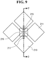
- FIG. 9 is a partially enlarged view of the touch sensing layer shown in FIG. 8
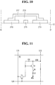
- FIG. 10 is a cross-sectional view of the touch sensing layer taken along line D-D' in FIG. 9 .
- the touch sensing layer 20 is disposed on the second substrate 12.
- the touch sensing layer 20 may include a sensing area SA capable of sensing a touch in a plan view and a non-sensing area NSA other than the sensing area SA.
- the sensing area SA may be an area overlapping the display area DA (refer to FIG. 1 ) of the display panel 10 (refer to FIG. 1 ), and the first portion 21 of the touch sensing layer 20 may be located in the sensing area SA.
- the non-sensing area NSA may be an area that does not sense the touch, and may be an area overlapping the non-display area NDA (refer to FIG. 1 ) of the display panel 10.
- the second portion 23 of the touch sensing layer 20 may be located in the non-sensing region NSA.
- the first portion 21 of the touch sensing layer 20 includes a plurality of touch electrodes, and the plurality of touch electrodes includes a plurality of first touch electrodes 211 and a plurality of second touch electrodes 213.
- the first touch electrode 211 and the second touch electrode 213 are separated from each other.
- the plurality of first touch electrodes 211 and the plurality of second touch electrodes 213 may be alternately and discretely arranged so as not to substantially overlap each other in the sensing area SA.
- the plurality of the first touch electrodes 211 may be arranged in the column direction and row direction, respectively, and the plurality of the second touch electrodes 213 may be arranged in the column direction and row direction, respectively.
- the first touch electrode 211 and the second touch electrode 213 may be located on the same layer, and may also be located on different layers.
- each of the first touch electrode 211 and the second touch electrode 213 may have a rectangular or rhombic shape, for example, but is not limited thereto.
- Each of the first touch electrode 211 and the second touch electrode 213 may have various shapes, such as protrusions for improving the sensitivity of the touch sensing layer 20.
- the plurality of first touch electrodes 211 arranged in the same row or column may be connected to each other inside or outside the sensing area SA, or may be separated from each other inside or outside the sensing area SA.
- at least some of the plurality of second touch electrodes 213 arranged in the same row or column may be connected to each other inside or outside the sensing area SA, or may be separated from each other inside or outside the sensing area SA.
- the plurality of second touch electrodes 213 arranged in the same column may be connected to each other in the sensing area SA, for example. More specifically, the plurality of first touch electrodes 211 arranged in each row is connected to each other through a first connection member 215, and the plurality of second touch electrodes 213 arranged in each column is connected to each other through a second connection member 217.
- the first connection member 215 connecting the first touch electrodes 211 adjacent to each other may be located in the same layer as the first touch electrode 211, and may include the same material as that of the first touch electrode 211. That is, the first touch electrode 211 and the first connection member 215 may be unitary with each other, and may be simultaneously patterned.
- the second connection member 217 connecting the second touch electrodes 213 adjacent to each other may be located on the different layer from the second touch electrode 213. That is, the second touch electrode 213 and the first connection member 215 may be separated from each other and separately patterned. The second touch electrode 213 and the second connection member 217 are connected to each other through direct contact.
- An insulating layer 219 is disposed between the first connection member 215 and the second connection member 217 to isolate the first connection member 215 and the second connection member 217 from each other.
- the insulating layer 219 may be a plurality of independent island-shaped insulators disposed for each intersection of the first connection member 215 and the second connection member 217.
- the insulating layer 219 may expose at least a part of the second touch electrode 213 such that the second connection member 217 is connected to the second touch electrode 213.
- the edge of the insulating layer 219 may have a rounded shape or a polygonal shape.
- the insulating layer 219 may include SiOx, SiNx, and/or SiOxNy, for example.
- the insulating layer 219 may be entirely provided, and the insulating layer 219 located on a part of the second touch electrode 213 may be removed for connection with the second touch electrode 213 adjacent in the column direction.
- the second connection member 217 connecting the second touch electrodes 213 adjacent to each other may be located in the same layer as the first touch electrode 211 and may be unitary with the first touch electrode 211, and the first connection member 215 connecting the first touch electrodes 211 adjacent to each other may be located on a different layer from the first touch electrode 211.
- the second portion 23 of the touch sensing layer 20 may include a first touch signal line 231 and a second touch signal line 233.
- the first touch electrodes 211 connected to each other for each row may be electrically connected to the touch driver 550 through the first touch signal line 231, and the second touch electrodes 213 connected to each other for each column may be electrically connected to the touch driver 550 through the second touch signal line 233.
- the end portions of the first touch signal line 231 and the second touch signal line 233 may form a pad portion 235 on the second substrate 12.
- the first touch electrode 211 and the second touch electrode 213 have a predetermined transmittance or more such that light emitted from the display layer of the display panel 10 is transmitted.
- the first touch electrode 211 and the second touch electrode 213 may include a thin metal layer such as indium tin oxide ("ITO"), indium zinc oxide (“IZO”), or silver nanowires (AgNw), or may include a transparent conductive material such as metal mesh or carbon nanotubes ("CNT").
- ITO indium tin oxide
- IZO indium zinc oxide
- AgNw silver nanowires
- CNT transparent conductive material
- the invention is not limited thereto.
- the materials of the first connection member 215 and the second connection member 217 are the same as those of the first touch electrode 211 and the second touch electrode 213.
- the first touch signal line 231 and the second touch signal line 233 may include the transparent conductive material included in the first touch electrode 211 and the second touch electrode 213, or may include a low-resistance material such as molybdenum (Mo), silver (Ag), titanium (Ti), copper (Cu), aluminum (Al), or molybdenum/aluminum/molybdenum (Mo/Al/Mo).
- Mo molybdenum
- Mo molybdenum
- Ag silver
- Ti titanium
- Cu copper
- Al aluminum
- Mo/Al/Mo molybdenum/aluminum/molybdenum
- the first touch electrode 211 and the second touch electrode 213 adjacent to each other form a mutual capacitance, and any one of the first touch electrode 211 and the second touch electrode 213 may output a change in mutual capacitance generated by an external object as a touch sensing signal.
- the first portion 21 and second portion 23 of the touch sensing layer 20 may be disposed on the second substrate 12 by patterning.
- the first touch electrode 211, the second touch electrode 213, the first touch signal line 231, the second touch signal line 233, and the pad portion 235 may be disposed directly on the second substrate 12, for example.
- the first touch electrode 211, the second touch electrode 213, the first touch signal line 231, the second touch signal line 233, and the pad portion 235 may disposed directly on the insulating layer.
- FIG. 11 is an exemplary equivalent circuit diagram of one pixel included in a display layer in a display device according to an exemplary embodiment
- FIG. 12 is an exemplary plan view of one pixel of a display device according to an exemplary embodiment
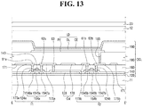
- FIG. 13 is a cross-sectional view taken along line E-E' in FIG. 12 .
- the display layer DCL includes a plurality of pixels PX, and one pixel PX includes a switching TFT T1, a driving TFT T2, a storage capacitor Cst, and a light-emitting element LD.
- the display device includes a plurality of signal lines 121, 171, and 172 and a plurality of pixels PX connected to the signal lines and arranged in a matrix form.
- the signal lines include a plurality of gate lines 121 which transmit a gate signal (or a scanning signal), a plurality of data lines 171 which transmit a data signal, and a plurality of driving voltage lines 172 which transmit a driving voltage VDD.
- the gate lines 121 extend substantially in the row direction and are substantially parallel to each other
- the data lines 171 extend substantially in the column direction and are substantially parallel to each other
- the driving voltage lines 172 extend substantially in the column direction and are substantially parallel to each other.
- the gate signal and the data signal may be applied through the display driver IC.
- the switching TFT T1 has a control terminal, an input terminal, and an output terminal.
- the control terminal is connected to the gate line 121
- the input terminal is connected to the data line 171
- the output terminal is connected to the driving TFT T2.
- the switching TFT T1 transmits a data signal applied to the data line 171 to the driving TFT T2 in response to a gate signal applied to the gate line 121.
- the driving TFT T2 also has a control terminal, an input terminal, and an output terminal.
- the control terminal is connected to the switching TFT T1
- the input terminal is connected to the driving voltage line 172
- the output terminal is connected to the light emitting element LD.
- the driving TFT T2 supplies an output current Id of which intensity varies according to the voltage applied between the control terminal and the output terminal of the driving TFT T2.
- the storage capacitor Cst is connected between the control terminal and input terminal of the driving TFT T2.
- the storage capacitor Cst charges the data signal applied to the control terminal of the driving TFT T2 and holds this state even after the switching TFT T1 is turned off.
- the light-emitting element LD which may be an organic light-emitting diode, includes a pixel electrode connected to the output terminal of the driving TFT T2 and a common electrode connected to a common voltage VSS.
- the light emitting element LD emits light with different intensity according to the output current Id of the driving TFT T2 to display an image.
- Each of the switching TFT T1 and the driving TFT T2 may be an n-channel field effect transistor ("FET") or a p-channel FET.
- FET field effect transistor
- the connection relationship of the switching TFT T1, the driving TFT T2, the storage capacitor Cst, and the light-emitting element LD may be changed.
- the display device includes a display layer DCL disposed on the first substrate 11, and the display layer DCL includes a light-emitting element LD.
- the display layer DCL includes a buffer layer 120, a switching semiconductor layer 154a, a driving semiconductor layer 154b, a gate insulating layer 140, a gate line 121, a first capacitor plate 128, an interlayer insulating layer, a data line 171, a driving voltage line 172, a switching drain electrode 175a, a driving drain electrode 175b, a protection film 180, a pixel defining film 190, and a light-emitting element LD.
- the buffer layer 120 may be disposed on the first substrate 11, may include silicon nitride (SiNx), silicon oxide (SiOx), or silicon oxynitride (SiOxNy), for example, and may be provided as a single layer or a multilayer.
- the buffer layer 120 serves to prevent the penetration of impurities, moisture, or external air deteriorating the characteristics of a semiconductor and to flatten a surface.
- the switching semiconductor layer 154a and the driving semiconductor layer 154b are disposed on the buffer layer 120 to be apart from each other.
- the switching semiconductor layer 154a and the driving semiconductor layer 154b include polycrystalline silicon, and include channel regions 1545a and 1545b, source regions 1546a and 1546b, and drain regions 1547a and 1547b.
- the source regions 1546a and 1546b and the drain regions 1547a and 1547b are disposed on both opposite sides of the channel regions 1545a and 1545b, respectively.
- the channel regions 1545a and 1545b include polycrystalline silicon not doped with impurities, that is, an intrinsic semiconductor.
- the source regions 1546a and 1546b and the drain regions 1547a and 1547b include polycrystalline silicon doped with conductive impurities, that is, an impurity semiconductor.
- a gate insulating layer 140 is disposed on the channel regions 1545a and 1545b of the switching semiconductor layer 154a and the driving semiconductor layer 154b.
- the gate insulating layer 140 may be a single layer or multilayer including at least one of silicon nitride and silicon oxide, for example.
- a gate line 121 is disposed on the gate insulating layer 140, and a first capacitor plate 128 is disposed on the buffer layer 120.
- the gate line 121 includes a switching gate electrode 124a extending in the lateral direction, transmitting a gate signal, and protruding from the gate line 121 toward the switching semiconductor layer 154a.
- the first capacitor plate 128 includes a driving gate electrode 124b protruding from the first capacitor plate 128 toward the driving semiconductor layer 154b.
- the switching gate electrode 124a and the driving gate electrode 124b overlap the channel regions 1545a and 1545b, respectively.
- An interlayer insulating layer 160 is disposed on the gate line 121, the first capacitor plate 128, and the buffer layer 120.
- a switching source contact hole 61a and a switching drain contact hole 62a are defined in the interlayer insulating layer 160 to expose the source region 1546a and the drain region 1547a of the switching semiconductor layer 154a, respectively.
- a driving source contact hole 61b and a driving drain contact hole 62b are defined in the interlayer insulating layer 160 to expose the source region 1546b and the drain region 1547b of the driving semiconductor layer 154b, respectively.
- a data line 171, a driving voltage line 172, a switching drain electrode 175a, and a driving drain electrode 175b are disposed on the interlayer insulating layer 160.
- the data line 171 extends in a direction (e.g., vertical direction in FIG. 12 ) crossing the gate line 121 and includes a switching source electrode 173a which extends in a direction (e.g., horizontal direction in FIG. 12 ) parallel to the gate line 121, transmits a data signal and protrudes from the data line 171 toward the switching semiconductor layer 154a.
- the driving voltage line 172 transmits a driving voltage, is separated from the data line 171, and extends in the same direction (e.g., vertical direction in FIG. 12 ) as that of the data line 171.
- the driving voltage line 172 includes a driving source electrode 173b protruding from the driving voltage line 172 toward the driving semiconductor layer 154b and a second capacitor plate protruding from the driving voltage line 172 to overlap the first capacitor plate 128.
- the first capacitor plate 128 and the second capacitor plate 178 may form a storage capacitor Cst by the interlayer insulating layer 160 as a dielectric.
- the switching drain electrode 175a faces the switching source electrode 173a
- the driving drain electrode 175b faces the driving source electrode 173b.
- the switching source electrode 173a and the switching drain electrode 175a are electrically connected to the source region 1546a and drain region 1547a of the switching semiconductor layer 154a through the switching source contact hole 61a and the switching drain contact hole 62a. Further, the switching drain electrode 175a extends to be electrically connected to the first capacitor plate 128 and the driving gate electrode 124b through the first contact hole 63 defined in the interlayer insulating layer 160.
- the driving source electrode 173b and the driving drain electrode 175b are electrically connected to the source region 1546b and drain region 1547b of the driving semiconductor layer 154b through the driving source contact hole 61b and the driving drain contact hole 62b.
- the switching semiconductor layer 154a, the switching gate electrode 124a, the switching source electrode 173a, and the switching drain electrode 175a constitute the switching TFT T1.
- the driving semiconductor layer 154b, the driving gate electrode 124b, the driving source electrode 173b, and the driving drain electrode 175b constitute the driving TFT T2.
- a protection film 180 is disposed on the data line 171, the driving voltage line 172, the switching drain electrode 175a, and the driving drain electrode 175b.
- a second contact hole 185 is defined in the protection film 180 to expose the driving drain electrode 175b.
- a light-emitting element LD and a pixel defining film 190 are disposed on the protection film 180.
- the light-emitting element LD includes a pixel electrode PE, an organic light-emitting layer OL, and a common electrode CE.
- the pixel electrode PE is disposed on the protection film 180, and is electrically connected to the driving drain electrode 175b of the driving TFT T2 through the second contact hole 185 defined in the protection film 180.
- the pixel electrode PE serves as an anode of the light-emitting element LD.
- the pixel electrode PE may include a transparent conductive material such as ITO, IZO, ZnO, or In 2 O3, or may include a reflective metal such as lithium (Li), calcium (Ca), lithium fluoride/calcium (LiF/Ca), lithium fluoride/aluminum (LiF/Al), aluminum (Al), silver (Ag), magnesium (Mg), or gold (Au).
- a transparent conductive material such as ITO, IZO, ZnO, or In 2 O3
- a reflective metal such as lithium (Li), calcium (Ca), lithium fluoride/calcium (LiF/Ca), lithium fluoride/aluminum (LiF/Al), aluminum (Al), silver (Ag), magnesium (Mg), or gold (Au).
- the pixel defining film 190 is disposed on the edge of the pixel electrode PE and the protection film 180. An opening for exposing the pixel electrode PE is defined in the pixel defining film 190.
- the pixel defining film 190 may include a resin such as polyacrylate or polyimide.
- An organic light-emitting layer OL is disposed on the pixel electrode PE in the opening of the pixel defining film 190.
- the organic light-emitting layer OL includes a light emitting layer and includes a plurality of layers including at least one of a hole injection layer ("HIL"), a hole transport layer (“HTL”), an electron transport layer (“ETL”), and an electron injection layer (“EIL").
- HIL hole injection layer
- HTL hole transport layer
- ETL electron transport layer
- EIL electron injection layer
- the organic light-emitting layer OL may include a red organic light-emitting layer emitting red light, a green organic light-emitting layer emitting green light, and a blue organic light-emitting layer emitting blue light.
- the red organic light-emitting layer, the green organic light-emitting layer, and the blue organic light-emitting layer are provided in a red pixel, a green pixel, and a blue pixel, respectively, to realize a color image.
- the organic light-emitting layer OL may realize a color image by laminating a red organic light-emitting layer, a green organic light-emitting layer and a blue organic light-emitting layer in a red pixel, a green pixel and a blue pixel, respectively, and forming a red color filter, a green color filter and a blue color filter for each pixel.
- the common electrode CE is disposed on the pixel defining film 190 and the organic light-emitting layer OL.
- the common electrode CE may include a transparent conductive material such as ITO, IZO, ZnO, or In 2 O 3 , or may include a metal such as lithium (Li), calcium (Ca), lithium fluoride/calcium (LiF/Ca), lithium fluoride/aluminum (LiF/Al), aluminum (Al), silver (Ag), magnesium (Mg), or gold (Au).
- the common electrode CE serves as a cathode of the light-emitting element LD.
- the second substrate 12 may be disposed on the display layer DCL, and the touch sensing layer 20 may be disposed on the second substrate 12.
- FIG. 14 is a plan view of a touch flexible circuit board included in a display device according to another exemplary embodiment
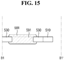
- FIG. 15 is a cross-sectional view of the touch flexible circuit board taken along B1-B1' in FIG. 14
- FIG. 16 is a cross-sectional view of a display device according to another exemplary embodiment taken along line B-B' in FIGS. 1 and 2 .
- a display device 2 according to this exemplary embodiment is different from the display device 1 described above with reference to FIGS. 1 to 13 in that it includes a touch flexible circuit board 50a, and other components of the display device 2 are substantially the same as those of the display device 1. Therefore, duplicate contents are omitted, and differences are mainly described.
- the touch flexible circuit board 50a is different from the touch flexible circuit board 50 shown in FIGS. 3 to 7 in that it further include a UV transmitting resin layer 581 provided in the opening member 59 as a UV transmitting member in addition to the opening member 59.
- Other components of the touch flexible circuit board 50a are substantially the same as or similar to those of the touch flexible circuit board 50.
- the UV transmitting resin layer 581 may include a material that transmits UV light. Therefore, when curing the bonding layer 70, the UV light UV emitted from the side surface of the display device 2 may be provided to the bonding layer 70 through the opening member 59 and the UV transmitting resin layer 581.
- the UV transmitting material may include a transparent organic material such as acrylic resin, for example, but is not limited thereto.
- the UV transmitting resin layer 581 may include a material that blocks visible light and transmits UV light.
- the UV transmitting resin layer 581 may fill each of the first opening 591, the second opening 593, the third opening 595, and the fourth opening 597.
- the UV transmitting resin layer 581 may be in contact with any one of the upper surface and lower surface of the second substrate member 530. Further, in some exemplary embodiments, as shown in the drawings, the UV transmitting resin layer 581 may be in contact with both the upper surface and lower surface of the second substrate member 530.
- the UV transmitting resin layer 581 may be provided in the form of being applied to the entire bending portion 530A. Since the UV- transmitting resin layer 581 is applied to the bending portion 530A, when the bending portion 530A is bent, not only tensile force but also compressive force from the UV transmitting resin layer 581 are applied to the touch flexible circuit board 50a at the same time. As a result, the tensile force and the compressive force are canceled each other, and the stress of the touch flexible circuit board 50a is minimized, so that it is possible to prevent the touch flexible circuit board 50a or the components (for example, wiring) provided in the touch flexible circuit board 50a from being damaged by bending.
- FIG. 17 is a plan view of a touch flexible circuit board included in a display device according to still another exemplary embodiment
- FIG. 18 is a cross-sectional view of the touch flexible circuit board taken along B1-B1' in FIG. 17
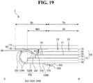
- FIG. 19 is a cross-sectional view of a display device according to still another exemplary embodiment taken along line B-B' in FIGS. 1 and 2 .
- a display device 3 according to this exemplary embodiment is different from the display device 2 described above with reference to FIGS. 14 to 16 in that it includes a touch flexible circuit board 50b, and other components of the display device 3 are substantially the same as those of the display device 2. Therefore, duplicate contents are omitted, and differences are mainly described.
- the touch flexible circuit board 50b is different from the touch flexible circuit board 50a shown in FIGS. 14 to 16 in that an UV transmitting resin layer 583 includes an UV transmitting resin 583a and light-scattering particles 583b dispersed in the UV transmitting resin 583a.
- an UV transmitting resin layer 583 includes an UV transmitting resin 583a and light-scattering particles 583b dispersed in the UV transmitting resin 583a.
- a description of the UV transmitting resin layer 583 is substantially the same as or similar to that of the UV transmitting resin layer 581 described above with reference to FIGS 14 to 16 . Therefore, hereinafter, differences will be mainly described.
- the UV transmitting resin layer 583 may include an UV transmitting resin 583a and light-scattering particles 583b dispersed in the UV transmitting resin 583a.
- the UV transmitting resin 583a may be an UV transmitting material.
- the UV transmitting material may include a transparent organic material such as acrylic resin, but is not limited thereto.
- the UV transmitting resin layer 581 may be a material that blocks visible light and transmits UV light.
- the light-scattering particles 583b may scatter or diffuse incident light.
- the light-scattering particles 583b may include at least one of ZrO 2 , TiO 2 , Al 2 O 3 , MgO, and SiO 2 , for example.
- the UV light emitted from the side of the display device 3 in the process of curing the bonding layer 70 may be provided to the bonding layer 70 through the opening member 59 and the UV transmitting resin layer 583. Further, since the UV transmitting resin layer 583 further includes the light-scattering particles 583b, the UV light having passed through the UV transmitting resin layer 583 may be scattered and diffused by the light-scattering particles 583b. Thus, uniform UV light may be provided to a portion of the bonding layer, overlapping the light blocking member 43, and the curing reliability of the bonding layer 70 may be improved.
- the structure of the touch flexible circuit board may be variously changed.
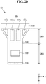
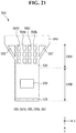
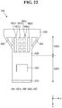
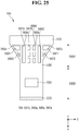
- FIGS. 20 to 25 are plan views showing touch flexible circuit boards according to modification embodiments of FIG. 3 .
- touch flexible circuit boards according to modification embodiments will be described with reference to FIGS. 20 to 25 .
- the edge of an opening included in an opening member 59a may be provided in a concavo-convex shape respectively a meander shape, especially a sawtooth shape or another shape with alternating protrusions and recesses.
- the edge of a first opening 591a, the edge of a second opening 593a, the edge of a third opening 595a, and the edge of a fourth opening 597a, which are included in an opening member 59a may be unevenly provided, for example. Accordingly, when UV light is laterally radiated in the process of curing the bonding layer 70, the UV light transmitted through the opening member 59a may be scattered/diffused at the edge where the irregularities are provided, and thus uniform UV light may be provided to the bonding layer 70.
- a touch flexible circuit board 50d according to this modification embodiment is different from the touch flexible circuit board 50 shown in FIG. 3 in the shape of an opening member 59b, and other components of the touch flexible circuit board 50d are substantially the same as those of the touch flexible circuit board 50.
- the opening member 59b of the touch flexible circuit board 50d may include a first opening area 591b, a second opening 593, a third opening area 595b, and a fourth opening 597.
- the first opening area 591b may include a plurality of sub-openings 5911, and the planar shapes of the sub-openings 5911 may be substantially the same as each other.
- the sub-openings 5911 may be spaced apart from each other, and may be arranged along the row and column directions.
- the third opening area 595b may also include a plurality of sub-openings 5951 spaced apart from each other in the row and column directions, and the planar shapes of the sub-openings 5951 may be substantially the same as each other.
- a touch flexible circuit board 50e according to this modification embodiment is different from the touch flexible circuit board 50d shown in FIG. 21 in the shape of an opening member 59c, and other components of the touch flexible circuit board 50e are substantially the same as those of the touch flexible circuit board 50d.
- the opening member 59c may include a first opening area 591c, a second opening 593, a third opening area 595c, and a fourth opening 597.
- the first opening area 591c includes a first sub-opening 5913 having a stripe shape and a plurality of second sub-openings 5915 having a smaller size than the first sub-opening 5913 and spaced apart from each other along the extension direction of the first sub-opening 5913.
- the third opening area 595c includes a third sub-opening 5953 having a stripe shape and a plurality of fourth sub-openings 5955 having a smaller size than the third sub-opening 5953 and spaced apart from each other along the extension direction of the third sub-opening 5953.
- the shape of the third opening area 595c and the shape of the first opening area 591c may be symmetrical to each other with respect to an imaginary line extending along the first direction x.
- a touch flexible circuit board 50f according to this modification embodiment is different from the touch flexible circuit board 50 shown in FIG. 3 in the shape of an opening member 59d, and other components of the touch flexible circuit board 50f are substantially the same as those of the touch flexible circuit board 50.
- the opening member 59d may include a first opening 591, a second opening area 593a, a third opening 595, and a fourth opening area 597a.
- the second opening area 593a includes a plurality of sub-openings 5931 and 5933, unlike the second opening 593 shown in FIG. 3 .
- the second opening area 593a may include a first sub-opening 5931 and a second sub-opening 5933 spaced apart from the first sub-opening 5931, for example.
- the first sub-opening 5931 and the second sub-opening 5933 may be spaced from each other along the first direction x, for example, but the invention is not limited thereto.
- the planar shape of the first sub-opening 5931 may be different from the planar shape of the second sub-opening 5933.
- the fourth opening area 597a may include a third sub-opening 5971 and a fourth sub-opening 5973 spaced apart from the third sub-opening 5971.
- the planar shape of the third sub-opening 5971 may be different from the planar shape of the fourth sub-opening 5973.
- a touch flexible circuit board 50g according to this modification embodiment is different from the touch flexible circuit board 50 shown in FIG. 3 in the shape of an opening member 59e, and other components of the touch flexible circuit board 50g are substantially the same as those of the touch flexible circuit board 50.
- the opening member 59e may include a first opening area 591b, a second opening area 593a, a third opening area 595b, and a fourth opening area 597a.
- a description of the first opening area 591b and the third opening area 595b is the same as that described with reference to FIG. 21
- a description of the second opening area 593a and the fourth opening area 597a is the same as that described in FIG. 23 . Therefore, these descriptions will be omitted.
- a touch flexible circuit board 50h according to this modification embodiment is different from the touch flexible circuit board 50 shown in FIG. 3 in the shape of an opening member 59f, and other components of the touch flexible circuit board 50h are substantially the same as those of the touch flexible circuit board 50.
- the opening member 59f may include a first opening area 591c, a second opening area 593a, a third opening area 595c, and a fourth opening area 597a.
- a description of the first opening area 591c and the third opening area 595c is the same as that described with reference to FIG. 22
- a description of the second opening area 593a and the fourth opening area 597a is the same as that described in FIG. 23 . Therefore, these descriptions will be omitted.
- each of the touch flexible circuit boards according to the modification embodiments, described with reference to FIGS. 21 to 25 may further include the UV transmitting resin layer 381 described with reference to FIGS. 14 to 16 or the UV transmitting resin layer 383 with reference to FIGS. 17 to 19 .
- a display device having improved reliability.
- a flexible circuit board capable of manufacturing a display device having improved reliability.
Landscapes
- Engineering & Computer Science (AREA)
- Theoretical Computer Science (AREA)
- General Engineering & Computer Science (AREA)
- Physics & Mathematics (AREA)
- General Physics & Mathematics (AREA)
- Microelectronics & Electronic Packaging (AREA)
- Human Computer Interaction (AREA)
- Manufacturing & Machinery (AREA)
- Optics & Photonics (AREA)
- Computer Networks & Wireless Communication (AREA)
- Devices For Indicating Variable Information By Combining Individual Elements (AREA)
- Liquid Crystal (AREA)
Abstract
Description
- Exemplary embodiments of the invention relate to a display device and a flexible circuit board.
- A display device visually displays data. The display device generally includes a display panel for displaying an image and a window disposed outside the display panel to protect the display panel. A bonding layer is disposed between the display panel and the window to attach the display panel and the window to each other.
- The bonding layer is applied to the window in a liquid phase, and is cured by ultraviolet light after the display panel and the window are laminated.
- Recently, the display device may include a touch sensing function interacting with a user in addition to a function of displaying the image. That is, a recent display device may further include a touch sensing layer and a flexible circuit board coupled to the touch sensing layer as well as the display panel, the window, and the bonding layer.
- In a case which a display device includes a touch sensing layer and a flexible circuit board coupled to the touch sensing layer as well as a bonding layer, a transmission of ultraviolet ("UV") light may be inhibited by the flexible circuit board around an area where the flexible circuit board is coupled to the touch sensing layer, and thus there is a possibility that a part of the bonding layer is not sufficiently cured, thereby deteriorating a reliability of the display device.
- Exemplary embodiments of the invention provide a display device having improved reliability.
- Other exemplary embodiments of the invention provide a flexible circuit board capable of manufacturing a display device having improved reliability.
- However, exemplary embodiments of the invention are not restricted to the one set forth herein. The above and other exemplary embodiments of the invention will become more apparent to one of ordinary skill in the art to which the invention pertains by referencing the detailed description of the invention given below.
- An exemplary embodiment may be related to a display device. The display device includes a display structure including a display panel and a touch sensing layer disposed on the display panel, the display panel including a display panel including a display area and a non-display area around the display area, and the touch sensing layer including a first portion overlapping the display area and a second portion overlapping the non-display area, a window structure disposed on the display structure, a bonding layer disposed between the display structure and the window structure, and a touch flexible circuit board electrically connected with the touch sensing layer, wherein the touch flexible circuit board includes a first substrate member connected to the second portion, and a second substrate member provided with an UV transmitting member transmitting UV light emitted from a side of the bonding layer and extending from the first substrate member in a predetermined direction.
- According to a preferred embodiment, the ultraviolet transmitting member does not overlap the touch sensing layer, that is, the ultraviolet transmitting member is in a plan view onto the touch sensing layer positioned outside the touch sensing layer.
- According to a preferred embodiment, the second substrate member includes a bending portion extending from the first substrate member and an extension portion extending from the bending portion and disposed under the display structure, and the ultraviolet transmitting member is defined at the bending portion. Preferably, the bending portion does not overlap the touch sensing layer, that is, the bending portion is in a plan view onto the touch sensing layer positioned outside the touch sensing layer.
- An exemplary embodiment may be related to a display device. The display device includes a display structure, a window, which also might be called window element, disposed on the display structure, a light blocking member disposed on one surface of the window facing the display structure, a bonding layer between the window and the display structure, and a flexible circuit board including a first substrate member and a second substrate member provided with an UV transmitting member overlapping the light blocking member and extending from the first substrate member.
- An exemplary embodiment may be related to a flexible circuit board. The flexible circuit board includes a first substrate member connected with an electronic device, a second substrate member extending from the first substrate member and provided with an opening member, and an UV transmitting resin layer provided in the opening member. The opening member may be also called an opening structure, especially an opening pattern.
- The above and other exemplary embodiments and features of the invention will become more apparent by describing in detail exemplary embodiments thereof with reference to the attached drawings, in which:
-
FIG. 1 is an exploded perspective view of an exemplary embodiment of a display device; -
FIG. 2 is a plan view of an exemplary embodiment of a display device; -
FIG. 3 is a plan view showing an exemplary embodiment of a state before bending of a touch flexible circuit board included in a display device; -
FIG. 4 is a cross-sectional view taken along line B1-B1' inFIG. 3 ; -
FIG. 5 is a cross-sectional view of the display device ofFIGS. 1 and2 taken along line A-A' inFIGS. 1 and2 ; -
FIG. 6 is a cross-sectional view of the display device ofFIGS. 1 and2 taken along line B-B' inFIGS. 1 and2 ; -
FIG. 7 is a cross-sectional view of the display device ofFIGS. 1 and2 taken along line C-C' inFIGS. 1 and2 ; -
FIG. 8 is a plan view showing an exemplary embodiment of a touch sensing layer of a display device; -
FIG. 9 is a partially enlarged view of the touch sensing layer shown inFIG. 8 ; -
FIG. 10 is a cross-sectional view of the touch sensing layer taken along line D-D' inFIG. 9 ; -
FIG. 11 is an equivalent circuit diagram of an exemplary embodiment of one pixel of a display device; -
FIG. 12 is an exemplary plan view of an exemplary embodiment of one pixel of a display device; -
FIG. 13 is a cross-sectional view taken along line E-E' inFIG. 12 ; -
FIG. 14 is a plan view showing another exemplary embodiment of a state before bending of a touch flexible circuit board included in a display device; -
FIG. 15 is a cross-sectional view of the touch flexible circuit board taken along B1-B1' inFIG. 14 ; -
FIG. 16 is a cross-sectional view of another exemplary embodiment of a display device taken along line B-B' inFIGS. 1 and2 ; -
FIG. 17 is a plan view showing another exemplary embodiment of a state before bending of a touch flexible circuit board included in a display device; -
FIG. 18 is a cross-sectional view of the touch flexible circuit board taken along B1-B1' inFIG. 17 ; -
FIG. 19 is a cross-sectional view of still another exemplary embodiment of a display device taken along line B-B' inFIGS. 1 and2 ; and -
FIGS. 20 to 25 are plan views showing states before bending of touch flexible circuit boards according to modified exemplary embodiments ofFIG. 3 . - The invention will now be described more fully hereinafter with reference to the accompanying drawings, in which preferred embodiments of the invention are shown. This invention may, however, be embodied in different forms and should not be construed as limited to the exemplary embodiments set forth herein. Rather, these embodiments are provided so that this invention will be thorough and complete, and will filly convey the scope of the invention to those skilled in the art. The same reference numbers indicate the same components throughout the specification. In the attached drawing figures, the thickness of layers and regions is exaggerated for clarity. Throughout the specification, the same reference numerals are used for the same or similar parts.
- It will also be understood that when a layer is referred to as being "on" another layer or substrate, it may be directly on the other layer or substrate, or intervening layers may also be present. In contrast, when an element is referred to as being "directly on" another element, there are no intervening elements present.
- Although the terms "first", "second", etc. may be used herein to describe various elements, these elements, should not be limited by these terms. These terms may be used to distinguish one element from another element. Thus, a first element discussed below may be termed a second element without departing from teachings of one or more embodiments. The description of an element as a "first" element may not require or imply the presence of a second element or other elements. The terms "first", "second", etc. may also be used herein to differentiate different categories or sets of elements. For conciseness, the terms "first", "second", etc. may represent "first-category (or first-set)", "second-category (or second-set)", etc., respectively.
- The use of the terms "a" and "an" and "the" and similar referents in the context of describing the invention (especially in the context of the following claims) are to be construed to cover both the singular and the plural, unless otherwise indicated herein or clearly contradicted by context. The terms "comprising," "having," "including," and "containing" are to be construed as open-ended terms (i.e., meaning "including, but not limited to,") unless otherwise noted.
- The invention will be described with reference to perspective views, cross-sectional views, and/or plan views, in which preferred embodiments of the invention are shown. Thus, the profile of an exemplary view may be modified according to manufacturing techniques and/or allowances. That is, the exemplary embodiments of the invention are not intended to limit the scope of the invention but cover all changes and modifications that can be caused due to a change in manufacturing process. Thus, regions shown in the drawings are illustrated in schematic form and the shapes of the regions are presented simply by way of illustration and not as a limitation.
- About" or "approximately" as used herein is inclusive of the stated value and means within an acceptable range of deviation for the particular value as determined by one of ordinary skill in the art, considering the measurement in question and the error associated with measurement of the particular quantity (i.e., the limitations of the measurement system). For example, "about" can mean within one or more standard deviations, or within ± 30%, 20%, 10%, 5% of the stated value.
- Unless otherwise defined, all terms (including technical and scientific terms) used herein have the same meaning as commonly understood by one of ordinary skill in the art to which this invention belongs. It will be further understood that terms, such as those defined in commonly used dictionaries, should be interpreted as having a meaning that is consistent with their meaning in the context of the relevant art and the invention, and will not be interpreted in an idealized or overly formal sense unless expressly so defined herein.
- Exemplary embodiments are described herein with reference to cross section illustrations that are schematic illustrations of idealized embodiments. As such, variations from the shapes of the illustrations as a result, for example, of manufacturing techniques and/or tolerances, are to be expected. Thus, embodiments described herein should not be construed as limited to the particular shapes of regions as illustrated herein but are to include deviations in shapes that result, for example, from manufacturing. In an exemplary embodiment, a region illustrated or described as flat may, typically, have rough and/or nonlinear features. Moreover, sharp angles that are illustrated may be rounded. Thus, the regions illustrated in the figures are schematic in nature and their shapes are not intended to illustrate the precise shape of a region and are not intended to limit the scope of the claims.
- Hereinafter, embodiments of the invention will be described with reference to the attached drawings.
-
FIG. 1 is an exploded perspective view of a display device according to an exemplary embodiment,FIG. 2 is a plan view of a display device according to an exemplary embodiment,FIG. 3 is a plan view showing a state before bending of a touch flexible circuit board included in a display device according to an exemplary embodiment,FIG. 4 is a cross-sectional view taken along line B1-B1' inFIG. 3 ,FIG. 5 is a cross-sectional view of the display device ofFIGS. 1 and2 taken along line A-A' inFIGS. 1 and2 ,FIG. 6 is a cross-sectional view of the display device ofFIGS. 1 and2 taken along line B-B' inFIGS. 1 and2 , andFIG. 7 is a cross-sectional view of the display device ofFIGS. 1 and2 taken along line C-C' inFIGS. 1 and2 . For reference, the line B1-B1' inFIG. 3 is a part of the line B-B' inFIGS. 1 and2 . - Referring to
FIGS. 1 to 6 , adisplay device 1 according to the illustrated exemplary embodiment may include a display structure DS, awindow structure 40 disposed over the display structure DS, abonding layer 70 disposed between thewindow structure 40 and the display structure DS, and a touchflexible circuit board 50 connected to the display structure DS. Thedisplay device 1 may further include a panelflexible circuit board 60 and a display driver IC, which are connected to the display structure DS. Thedisplay device 1 may further include apanel protection member 80 disposed beneath the display structure DS. - The display structure may include a
display panel 10 and atouch sensing layer 20, and may further include anoptical member 30. - In some exemplary embodiments, the
display panel 10 may have a rectangular shape in a plan view. Thedisplay panel 10 may include both opposite long sides extending in the first direction x and both opposite short sides extending in the second direction y intersecting the first direction x. The corner where the long side and short side of thedisplay panel 10 meet each other may have a right angle, but is not limited thereto, and may have a curved surface. The corner of thedisplay panel 10 may also be chamfered to reduce the risk of breakage. In addition, the planar shape of thedisplay panel 10 is not limited to the illustrated one, and may include various other shapes such as a circular shape. - The
display panel 10 includes a display area DA and a non-display area NDA in a plan view. The display area DA is an area where an image is displayed, and the non-display area NDA is an area where an image is not displayed. In some exemplary embodiments, the non-display area NDA may be disposed around the display area DA, and may surround the display area DA. - Unless defined otherwise, in this specification, the terms "on", "over", "upper side", "upper surface", or "top" means a side facing an arrow in the third directions z intersecting the first direction x and the second direction y based on the drawings, and the terms "beneath", "under", "lower side", "lower surface", or "bottom" means a side opposite to the side facing the arrow in the third direction z based on the drawings.
- In view of a laminate structure, the
display panel 10 includes afirst substrate 11, asecond substrate 12 disposed over thefirst substrate 11 and attached to thefirst substrate 11, and a display layer disposed between thefirst substrate 11 and thesecond substrate 12. - The
first substrate 11 is a substrate for supporting the display layer. In an exemplary embodiment, thefirst substrate 11 may include a polymer film such as glass or plastic. - The display layer is disposed on the
first substrate 11 and is located in the display area DA. The display layer may include a plurality of pixels and a plurality of display signal lines. Each pixel may include a thin film transistor ("TFT"), a capacitor, and a light emitting element, which will be described later. The plurality of display signal lines may include a gate line to transmit a gate signal to each pixel and a data line to transmit a data signal to each pixel. The display signal line may extend to the non-display area NDA. - In the non-display area NDA, the display driver IC may be disposed on the
first substrate 11. The display driver IC may include at least one of a data driver for applying a data signal to a data line, a gate driver for applying a gate signal to a gate line, and a signal control member for controlling the operations of the data driver and the gate driver. The display driver IC may be electrically connected with the display layer through the display signal line extending to the non-display area NDA or a separate wiring. In some exemplary embodiments, the display driver IC may be located adjacent to the short side of thefirst substrate 11 in the non-display area NDA. - In some exemplary embodiments, the display driver IC may be disposed (e.g., mounted) on the
first substrate 11. In an exemplary embodiment, when thefirst substrate 11 includes glass, for example, the display driver IC may be disposed (e.g., mounted) on thefirst substrate 11 in the form of a chip on glass ("COG"). In an alternative exemplary embodiment, when thefirst substrate 11 includes plastic, for example, the display driver IC may also be disposed (e.g., mounted) on thefirst substrate 11 in the form of a chip on plastic ("COP"). However, the invention is not limited thereto, and, in another exemplary embodiment, the display driver IC may be disposed on the panelflexible circuit board 60, or may be disposed on a separate main circuit board (not shown). Hereinafter, a case where the display driver IC is disposed (e.g., mounted) on thefirst substrate 11 in the non-display area NDA will be described as an example. - The
second substrate 12 may be an encapsulation substrate for preventing moisture and/or oxygen from penetrating into the display member from the outside. In an exemplary embodiment, thesecond substrate 12 may include a polymer film such as glass or plastic. Thesecond substrate 12 may be smaller than thefirst substrate 11, and may cover thefirst substrate 11 and the display member in the display area DA. In some exemplary embodiments, thesecond substrate 12 may be attached to thefirst substrate 11 by a sealant (not shown) applied along the edge of thesecond substrate 12 in the non-display area NDA. - In another exemplary embodiment, a thin film encapsulation layer in which at least one organic film and at least one inorganic film are alternately laminated one by one may be provided instead of the
second substrate 12. - The
touch sensing layer 20 may be disposed on thedisplay panel 10. In some exemplary embodiments, thetouch sensing layer 20 may obtain the coordinates of a touch input point in a capacitive manner. In the capacitive manner, the coordinate information of the touched point may be obtained in a self capacitive manner or a mutual capacitive manner. Hereinafter, for convenience of explanation, a case where thetouch sensing layer 20 has a mutual capacitive structure will be described as an example, but the invention is not limited thereto. - The
touch sensing layer 20 may be disposed on thesecond substrate 12 of thedisplay panel 10, and may include afirst portion 21 overlapping the display area DA of thedisplay panel 10 and asecond portion 23 overlapping the non-display area NDA of thedisplay panel 10. - The
first portion 21 of thetouch sensing layer 20 may include a touch electrode (not shown), and thesecond portion 23 thereof may include a touch signal line (not shown) to transmit and/or receiving a signal to/from the touch electrode and a pad portion provided by the extension of the touch signal line. In some exemplary embodiments, the touch electrode, touch signal line and pad portion of thetouch sensing layer 20 may be disposed directly on thesecond substrate 12. In other words, a separate bonding layer (for example, an adhesive layer) may not be disposed between thetouch sensing layer 20 and thesecond substrate 12. - The
optical member 30 may be disposed on thetouch sensing layer 20. In some exemplary embodiments, theoptical member 30 may include at least one of a phase retardation member and a polarization member. When theoptical member 30 includes both the phase retardation member and the polarization member, the polarization member may be disposed on the phase retardation member. External light incident from the outside of thewindow structure 40 passes through the polarization member to be linearly polarized. The linearly polarized incident light passes through the phase retardation member, is reflected, is incident on the phase retardation member again, passes through the phase retardation member again and then is incident on the polarization member. The linearly polarized incident light passes through the phase retardation member to have a phase difference of about 45°, and is circularly polarized to change its phase. As a result, after the external light passes through the phase retardation member again, most of the external light disappears without passing through the polarization member. In an exemplary embodiment, right-turn circularly polarized light having passed through the phase retardation member is reflected and converted into left-turn circularly polarized light, and the right-turn circularly polarized light and the left-turn circularly polarized light may disappear by destructive interference, for example. Therefore, the external light reflectance of thedisplay device 1 may decrease. However, the invention is not limited thereto, and, in another exemplary embodiment, theoptical member 30 may be omitted. In still another exemplary embodiment, theoptical member 30 may be disposed in thedisplay panel 10 instead of being disposed on thetouch sensing layer 20. Hereinafter, a case where theoptical member 30 is disposed on thetouch sensing layer 20 will be described as an example. - The
panel protection member 80 may be disposed under the display structure DS. - The
panel protection member 80 may include at least one of a buffer member and a heat radiation member. The buffer member may include a material having a high shock absorption rate. In an exemplary embodiment, the buffer member may include a polymer resin, such as polyurethane, polycarbonate, polypropylene, or polyethylene, or may be a sponge obtained by foam-molding a rubber liquid, a urethane-based material or an acrylic material. However, the invention is not limited thereto. - In an exemplary embodiment, the heat radiation member may include at least one of graphite, copper (Cu), and aluminum (Al), having good heat radiation characteristics, for example, but is not limited thereto. The heat radiation member not only improves the heat radiation characteristics but also has electromagnetic wave blocking or electromagnetic wave absorbing characteristics. In some exemplary embodiments, the
panel protection member 80 may be attached to the display structure DS through an adhesive layer, a double-sided adhesive tape, or the like. - The panel
flexible circuit board 60 may be connected to thedisplay panel 10 of the display structure DS. The panelflexible circuit board 60 is a component to which a signal for controlling the display driver IC or the display layer is applied, and the panelflexible circuit board 60 may be connected to thefirst substrate 11 in the non-display area NDA. - The panel
flexible circuit board 60 may include a firstpanel substrate member 610, a secondpanel substrate member 630, aconnection member 650, and aninput member 670. - The first
panel substrate member 610 is a portion of the panelflexible circuit substrate 60 connected to thefirst substrate 11 in the non-display area NDA. The firstpanel substrate member 610 may be connected to the pad portion (not shown) provided on thefirst substrate 11, and, in some exemplary embodiments, may be connected to the pad portion through an anisotropic conductive film or the like. However, the invention is not limited thereto, and the firstpanel substrate member 610 may be connected to the pad portion (not shown) provided on thefirst substrate 11 by an ultrasonic bonding method or the like, for example. The firstpanel substrate member 610 may be located at a portion adjacent to one short side of thefirst substrate 11 extending along the second direction y in the non-display area NDA. - The second
panel substrate member 630, which is a portion extending from the firstpanel substrate member 610, may extend along the first direction x from the firstpanel substrate member 610 and may be bent toward the lower side of the display structure DS or the lower side of thepanel protection member 80. That is, a part of the secondpanel substrate member 630 may include a bent portion extending from the firstpanel substrate member 610 and a portion extending from the bent portion and located under the display structure DS or thepanel protection member 80. - The
connection member 650 may be disposed on the secondpanel substrate member 630, and, in some exemplary embodiments, may overlap the display structure DS or thepanel protection member 80. Theconnection member 650 may be a portion connected to the touchflexible circuit board 50 to be described later. In some exemplary embodiments, theconnection member 650 may be provided in the form of a connector or the like. In an exemplary embodiment, when aconnection member 570 included in the touchflexible circuit board 50 is provided in a form of a female connector, theconnection member 650 may be provided in a form of a male connector, for example. Further, when theconnection member 570 included in the touchflexible circuit board 50 is provided in the form of a male connector, theconnection member 650 may be provided in the form of a female connector. However, this is merely an example, and the form of theconnection member 650 is not limited thereto. - The
input member 670 is a portion receiving a signal from the outside, and, in some exemplary embodiments, may be connected to a main circuit board (not shown). In some exemplary embodiments, theinput member 670 may be part of the secondpanel substrate member 630 or may be disposed on the secondpanel substrate member 630. - The touch
flexible circuit board 50 may be electrically connected to thetouch sensing layer 20 of the display structure DS. - The touch
flexible circuit board 50 may include afirst substrate member 510 and asecond substrate member 530, and may further include atouch driver 550 and aconnection member 570. - The
first substrate member 510 may be connected to thesecond portion 23 of thetouch sensing layer 20, overlapping the non-display region NDA, and, in some exemplary embodiments, may be connected to the pad portion of thesecond portion 23 of thetouch sensing layer 20. In some exemplary embodiments, thefirst substrate member 510 may be connected to thesecond portion 23 through an anisotropic conductive film or the like. However, the invention is not limited thereto, and thefirst substrate member 510 may be connected to thesecond portion 23 by various methods such as ultrasonic bonding. In some exemplary embodiments, thefirst substrate member 510 may be located at the same side as a portion of the display structure DS where the firstpanel substrate member 610 is disposed, but the invention is not limited thereto. - The
second substrate member 530 is a portion extending from thefirst substrate member 510 and not being connected to thetouch sensing layer 20. Thesecond substrate member 530 may be bent toward the lower side of the display structure DS or the lower side of thepanel protection member 80. That is, thesecond substrate member 530 may include a bendingportion 530A extending from thefirst substrate member 510 and anextension portion 530B extending from the bendingportion 530A. In some exemplary embodiments, thefirst substrate member 510 and theextension portion 530B may be provided in a substantially flat shape while the touchflexible circuit board 50 is bent, and the bendingportion 530A may be provided in a bent shape. - The bending
portion 530A may extend along the first direction x from thefirst substrate member 510, and may not overlap thetouch sensing layer 20 in the plan view. Further, the bendingportion 530A may overlap alight blocking member 43 of thewindow structure 40, which will be described later. In some exemplary embodiments, the bendingportion 530A may include a portion of which a width in the second direction y varies along the first direction x. In an exemplary embodiment, the bendingportion 530A may include a portion of which a width in the second direction y decreases as the portion is farther from thefirst substrate member 510 along the first direction x, for example. - The
extension portion 530B may extend from the bendingportion 530A and be located under the display structure DS or thepanel protection member 80. In some exemplary embodiments, theextension portion 530B may overlap thesecond portion 23 of thetouch sensing layer 20, and may further overlap thefirst portion 21 of thetouch sensing layer 20 or the display area DA of thedisplay panel 10. - The
touch driver 550 may transmit a touch driving signal to thetouch sensing layer 20. Thetouch driver 550 may process a touch sensing signal received from thetouch sensing layer 20 to generate touch information such as whether to touch and touch position. In some exemplary embodiments, thetouch driver 550 may be disposed (e.g., mounted) on theextension portion 530B. - The
second substrate member 530 may be provided with theconnection member 570. In some exemplary embodiments, theconnection member 570 may be provided on theextension portion 530B of thesecond substrate member 530. In some exemplary embodiments, theconnection member 570 may be connected to theconnection member 650 of the panelflexible circuit board 60. Thus, the touchflexible circuit board 50 may receive an external signal input through theinput member 670 of the panelflexible circuit board 60 and/or a signal generated/processed by the circuit element of the panelflexible circuit board 60. In some exemplary embodiments, theconnection member 570 may be provided in the form of a connector, as described above. - The
second substrate member 530 may be provided with an ultraviolet ("UV") transmitting member. The UV transmitting member transmits UV light emitted from the side surface of thebonding layer 70 when curingbonding layer 70. In some exemplary embodiments, the UV transmitting member may be composed of an openingmember 59 defined in thesecond substrate member 530. The openingmember 59 may be defined in a form of a hole penetrating the touchflexible circuit board 50, and may be defined in the bendingportion 530A of thesecond substrate member 530. Since the bendingportion 530A may overlap thelight blocking member 43 of thewindow structure 40, the openingmember 59 may also overlap thelight blocking member 43. Further, since the bendingportion 530A may not overlap thetouch sensing layer 20, the openingmember 59 may also not overlap thetouch sensing layer 20. The openingmember 59 may be also called anopening structure 59 oropening pattern 59. - The opening
member 59 may include one or more openings. In an exemplary embodiment, the openingmember 59 may include afirst opening 591 and asecond opening 593, and may further include athird opening 595 and afourth opening 597, for example. - In some exemplary embodiments, the
second opening 593, compared to thefirst opening 591, may be located adjacent to the edge of the bendingportion 530A. In other words, the minimum distance along the second direction y between thesecond opening 593 and the edge of the bendingportion 530A may be shorter than the minimum distance along the second direction y between the edge of thefirst opening 591 and the edge of the bendingportion 530A. - When the bending
portion 530A includes a portion of which a width in the second direction y varies along the first direction x, the planar shapes of thefirst opening 591 and thesecond opening 593 may be different from each other. In an exemplary embodiment, when thefirst opening 591 has a rectangular shape in which the width of thefirst opening 591 in the second direction is constant along the first direction x, thesecond opening 593 may have a triangular shape in which the width of thesecond opening 593 in the second direction decreases along the first direction x, for example. However, this is merely an example, and, in another exemplary embodiment, thefirst opening 591 and thesecond opening 593 may have the same shape. - In some exemplary embodiments, the
third opening 595 may have a shape symmetrical to thefirst opening 591 with respect to an imaginary line extending along the first direction x, and thefourth opening 597 may have a shape symmetrical to thesecond opening 593 with respect to an imaginary line extending along the first direction x. However, this is merely an example, and the shapes of thethird opening 595 and thefourth opening 597 may be variously changed. - Although the case where the opening
member 59 includes four openings has been described as an example, the number of openings included in the openingmember 59 may be variously changed. In an exemplary embodiment, the number of openings included in the openingmember 59 may be one, two, three, five or more, for example. - The
window structure 40 is disposed over the display structure DS to protect the display structure DS from external shocks and scratches. Thewindow structure 40 may include a light transmitting area TA and a light blocking area BA in a plan view. The light transmitting area TA is an area through which light is transmitted, and an image provided from thedisplay panel 10 may be transmitted to a user through the light transmitting area TA. The light blocking area BA may be an area for blocking light transmission. In some exemplary embodiments, the light blocking area BA may be located around the light transmitting area TA, and may surround the light transmitting area TA. In some exemplary embodiments, the light transmitting area TA may overlap the display area DA of thedisplay panel 10 and may not overlap the non-display area NDA of thedisplay panel 10. Further, the light blocking area BA may overlap the non-display area NDA of thedisplay panel 10 and may not overlap the display area DA of thedisplay panel 10. That is, the light blocking area BA may cover the non-display area NDA of thedisplay panel 10. - In view of a laminate structure, the
window structure 40 may include a window (or window element) 41 and alight blocking member 43. - The
light blocking member 43 may be disposed on one surface of thewindow 41 facing the display structure DS. Thelight blocking member 43 may define the light blocking area BA of thewindow structure 40. In some exemplary embodiments, thelight blocking member 43 may be a colored organic layer, and may be disposed on one side of thewindow 41 by coating, printing, or the like. In another exemplary embodiment, thelight blocking member 43 is disposed on a base layer such as a transparent film, and the base layer on which thelight blocking member 43 is disposed may be attached to one side of thewindow 41. - The
bonding layer 70 may be disposed between thewindow structure 40 and the display structure DS to couple thewindow structure 40 with the display structure DS. Thebonding layer 70 may be provided to fill the entire space between the light transmitting area TA of thewindow structure 40 and the display structure DS. In some exemplary embodiments, thebonding layer 70 may be provided to further fill a part of the space between the light blocking area BA of thewindow structure 40 and the display structure DS. - The
bonding layer 70 may include an UV-curable resin. In some exemplary embodiments, thebonding layer 70 may include an optical clear resin ("OCR"). Thebonding layer 70 may be first applied to thewindow structure 40 in a liquid or paste state, and may be cured by UV light after the display structure DS is laminated. - The
bonding layer 70 may be in contact with one surface of thewindow 41 of thewindow structure 40. When theoptical member 30 is disposed on thetouch sensing layer 20, thebonding layer 70 may further be in contact with the upper surface of theoptical member 30. - Since the
bonding layer 70 may initially have a liquid or paste state, spreading may occur when the display structure DS and thewindow structure 40 are coupled. Thus, thebonding layer 70 may further be in contact with one surface of thelight blocking member 43, and may further be in contact with the side surface of theoptical member 30. - In some exemplary embodiments, the
bonding layer 70 may further be in contact with a portion of thesecond portion 23 of thetouch sensing layer 20, the portion not overlapping theoptical member 30. - In some exemplary embodiments, the
bonding layer 70 may further be in contact with the side surface and top surface of thefirst substrate member 510 of the touchflexible circuit board 50 connected to thesecond portion 23 of thetouch sensing layer 20. In other words, thebonding layer 70 may further cover a part of thefirst substrate member 510. Accordingly, the connection reliability between thefirst substrate member 510 and thetouch sensing layer 20 may be improved. - When curing the
bonding layer 70, UV light may be applied to thebonding layer 70 from the top and side of thedisplay device 1. A portion of thebonding layer 70, overlapping the light transmitting area TA, may be cured by UV light provided from the top of thedisplay device 1. Since the UV light UV provided from the upper portion of thedisplay device 1 is blocked by thelight blocking member 43 at a portion of thebonding layer 70 overlapping the light blocking area BA, it is possible to cure a portion of thebonding layer 70 overlapping the light blocking area BA by the irradiation of UV light at the side of thebonding layer 70 or at the side of thedisplay device 1. - Accordingly, when the
bonding layer 70 is cured by the irradiation of UV light at the side of thedisplay device 1 or at the side of thebonding layer 70, there is a high possibility that a part of the UV light is blocked by the touchflexible circuit board 50, particularly, the bendingportion 530A of the touchflexible circuit board 50. Thus, there is a possibility that a part of thebonding layer 70 is uncured. In the case of thedisplay device 1 according to this exemplary embodiment, the touchflexible circuit board 50 is provided with the openingmember 59 as an UV transmitting member, so that the UV light emitted from the side of thebonding layer 70 passes through theopening 59 and is provided to thebonding layer 70. Therefore, it is possible to prevent thebonding layer 70 from being uncured and to improve the curing degree of thebonding layer 70, and thus it is possible to improve the reliability of thedisplay device 1. - In addition, since the
second substrate member 530 including the bendingportion 530A of the touchflexible circuit board 50 is provided with the openingmember 59, there is an advantage that the bending stress of the touchflexible circuit board 50 may be reduced, and thus there is an advantage that a possibility of lifting the touchflexible circuit board 50 or damaging the touchflexible circuit board 50 due to bending stress. Thus, there is an advantage that reliability of thedisplay device 1 may be further improved. - Hereinafter, a touch sensing layer will be described in more detail with reference to
FIGS. 8 to 10 . -
FIG. 8 is a plan view showing a touch sensing layer of a display device according to an exemplary embodiment,FIG. 9 is a partially enlarged view of the touch sensing layer shown inFIG. 8 , andFIG. 10 is a cross-sectional view of the touch sensing layer taken along line D-D' inFIG. 9 . - Referring to
FIG. 8 , thetouch sensing layer 20 is disposed on thesecond substrate 12. Thetouch sensing layer 20 may include a sensing area SA capable of sensing a touch in a plan view and a non-sensing area NSA other than the sensing area SA. The sensing area SA may be an area overlapping the display area DA (refer toFIG. 1 ) of the display panel 10 (refer toFIG. 1 ), and thefirst portion 21 of thetouch sensing layer 20 may be located in the sensing area SA. The non-sensing area NSA may be an area that does not sense the touch, and may be an area overlapping the non-display area NDA (refer toFIG. 1 ) of thedisplay panel 10. Thesecond portion 23 of thetouch sensing layer 20 may be located in the non-sensing region NSA. - The
first portion 21 of thetouch sensing layer 20 includes a plurality of touch electrodes, and the plurality of touch electrodes includes a plurality offirst touch electrodes 211 and a plurality ofsecond touch electrodes 213. Thefirst touch electrode 211 and thesecond touch electrode 213 are separated from each other. - The plurality of
first touch electrodes 211 and the plurality ofsecond touch electrodes 213 may be alternately and discretely arranged so as not to substantially overlap each other in the sensing area SA. The plurality of thefirst touch electrodes 211 may be arranged in the column direction and row direction, respectively, and the plurality of thesecond touch electrodes 213 may be arranged in the column direction and row direction, respectively. - The
first touch electrode 211 and thesecond touch electrode 213 may be located on the same layer, and may also be located on different layers. In an exemplary embodiment, each of thefirst touch electrode 211 and thesecond touch electrode 213 may have a rectangular or rhombic shape, for example, but is not limited thereto. Each of thefirst touch electrode 211 and thesecond touch electrode 213 may have various shapes, such as protrusions for improving the sensitivity of thetouch sensing layer 20. - The plurality of
first touch electrodes 211 arranged in the same row or column may be connected to each other inside or outside the sensing area SA, or may be separated from each other inside or outside the sensing area SA. Similarly, at least some of the plurality ofsecond touch electrodes 213 arranged in the same row or column may be connected to each other inside or outside the sensing area SA, or may be separated from each other inside or outside the sensing area SA. In an exemplary embodiment, as shown inFIG. 8 , when the plurality offirst touch electrodes 211 arranged in the same row are connected to each other inside the sensing area SA, the plurality ofsecond touch electrodes 213 arranged in the same column may be connected to each other in the sensing area SA, for example. More specifically, the plurality offirst touch electrodes 211 arranged in each row is connected to each other through afirst connection member 215, and the plurality ofsecond touch electrodes 213 arranged in each column is connected to each other through asecond connection member 217. - Referring to
FIGS. 9 and10 , thefirst connection member 215 connecting thefirst touch electrodes 211 adjacent to each other may be located in the same layer as thefirst touch electrode 211, and may include the same material as that of thefirst touch electrode 211. That is, thefirst touch electrode 211 and thefirst connection member 215 may be unitary with each other, and may be simultaneously patterned. - The
second connection member 217 connecting thesecond touch electrodes 213 adjacent to each other may be located on the different layer from thesecond touch electrode 213. That is, thesecond touch electrode 213 and thefirst connection member 215 may be separated from each other and separately patterned. Thesecond touch electrode 213 and thesecond connection member 217 are connected to each other through direct contact. - An insulating
layer 219 is disposed between thefirst connection member 215 and thesecond connection member 217 to isolate thefirst connection member 215 and thesecond connection member 217 from each other. As shown inFIGS. 9 and10 , the insulatinglayer 219 may be a plurality of independent island-shaped insulators disposed for each intersection of thefirst connection member 215 and thesecond connection member 217. The insulatinglayer 219 may expose at least a part of thesecond touch electrode 213 such that thesecond connection member 217 is connected to thesecond touch electrode 213. The edge of the insulatinglayer 219 may have a rounded shape or a polygonal shape. In an exemplary embodiment, the insulatinglayer 219 may include SiOx, SiNx, and/or SiOxNy, for example. - The insulating
layer 219 may be entirely provided, and the insulatinglayer 219 located on a part of thesecond touch electrode 213 may be removed for connection with thesecond touch electrode 213 adjacent in the column direction. - Unlike those shown in
FIGS. 9 and10 , thesecond connection member 217 connecting thesecond touch electrodes 213 adjacent to each other may be located in the same layer as thefirst touch electrode 211 and may be unitary with thefirst touch electrode 211, and thefirst connection member 215 connecting thefirst touch electrodes 211 adjacent to each other may be located on a different layer from thefirst touch electrode 211. - Referring back to
FIG. 8 , thesecond portion 23 of thetouch sensing layer 20 may include a firsttouch signal line 231 and a secondtouch signal line 233. - The
first touch electrodes 211 connected to each other for each row may be electrically connected to thetouch driver 550 through the firsttouch signal line 231, and thesecond touch electrodes 213 connected to each other for each column may be electrically connected to thetouch driver 550 through the secondtouch signal line 233. The end portions of the firsttouch signal line 231 and the secondtouch signal line 233 may form apad portion 235 on thesecond substrate 12. - The
first touch electrode 211 and thesecond touch electrode 213 have a predetermined transmittance or more such that light emitted from the display layer of thedisplay panel 10 is transmitted. In an exemplary embodiment, thefirst touch electrode 211 and thesecond touch electrode 213 may include a thin metal layer such as indium tin oxide ("ITO"), indium zinc oxide ("IZO"), or silver nanowires (AgNw), or may include a transparent conductive material such as metal mesh or carbon nanotubes ("CNT"). However, the invention is not limited thereto. The materials of thefirst connection member 215 and thesecond connection member 217 are the same as those of thefirst touch electrode 211 and thesecond touch electrode 213. - In an exemplary embodiment, the first
touch signal line 231 and the secondtouch signal line 233 may include the transparent conductive material included in thefirst touch electrode 211 and thesecond touch electrode 213, or may include a low-resistance material such as molybdenum (Mo), silver (Ag), titanium (Ti), copper (Cu), aluminum (Al), or molybdenum/aluminum/molybdenum (Mo/Al/Mo). - The
first touch electrode 211 and thesecond touch electrode 213 adjacent to each other form a mutual capacitance, and any one of thefirst touch electrode 211 and thesecond touch electrode 213 may output a change in mutual capacitance generated by an external object as a touch sensing signal. - In some exemplary embodiments, the
first portion 21 andsecond portion 23 of thetouch sensing layer 20 may be disposed on thesecond substrate 12 by patterning. In an exemplary embodiment, thefirst touch electrode 211, thesecond touch electrode 213, the firsttouch signal line 231, the secondtouch signal line 233, and thepad portion 235 may be disposed directly on thesecond substrate 12, for example. When the insulating layer disposed directly on thesecond substrate 12, thefirst touch electrode 211, thesecond touch electrode 213, the firsttouch signal line 231, the secondtouch signal line 233, and thepad portion 235 may disposed directly on the insulating layer. - Hereinafter, a display layer of a display device according to an exemplary embodiment of the invention will be described in detail with reference to
FIGS. 11 to 13 . -
FIG. 11 is an exemplary equivalent circuit diagram of one pixel included in a display layer in a display device according to an exemplary embodiment,FIG. 12 is an exemplary plan view of one pixel of a display device according to an exemplary embodiment, andFIG. 13 is a cross-sectional view taken along line E-E' inFIG. 12 . - As described above, the display layer DCL includes a plurality of pixels PX, and one pixel PX includes a switching TFT T1, a driving TFT T2, a storage capacitor Cst, and a light-emitting element LD.
- Specifically, referring to
FIG. 11 , the display device includes a plurality ofsignal lines - The signal lines include a plurality of
gate lines 121 which transmit a gate signal (or a scanning signal), a plurality ofdata lines 171 which transmit a data signal, and a plurality of drivingvoltage lines 172 which transmit a driving voltage VDD. The gate lines 121 extend substantially in the row direction and are substantially parallel to each other, thedata lines 171 extend substantially in the column direction and are substantially parallel to each other, and the drivingvoltage lines 172 extend substantially in the column direction and are substantially parallel to each other. The gate signal and the data signal may be applied through the display driver IC. - The switching TFT T1 has a control terminal, an input terminal, and an output terminal. The control terminal is connected to the
gate line 121, the input terminal is connected to thedata line 171, and the output terminal is connected to the driving TFT T2. The switching TFT T1 transmits a data signal applied to thedata line 171 to the driving TFT T2 in response to a gate signal applied to thegate line 121. - The driving TFT T2 also has a control terminal, an input terminal, and an output terminal. The control terminal is connected to the switching TFT T1, the input terminal is connected to the driving
voltage line 172, and the output terminal is connected to the light emitting element LD. The driving TFT T2 supplies an output current Id of which intensity varies according to the voltage applied between the control terminal and the output terminal of the driving TFT T2. - The storage capacitor Cst is connected between the control terminal and input terminal of the driving TFT T2. The storage capacitor Cst charges the data signal applied to the control terminal of the driving TFT T2 and holds this state even after the switching TFT T1 is turned off.
- The light-emitting element LD, which may be an organic light-emitting diode, includes a pixel electrode connected to the output terminal of the driving TFT T2 and a common electrode connected to a common voltage VSS. The light emitting element LD emits light with different intensity according to the output current Id of the driving TFT T2 to display an image.
- Each of the switching TFT T1 and the driving TFT T2 may be an n-channel field effect transistor ("FET") or a p-channel FET. The connection relationship of the switching TFT T1, the driving TFT T2, the storage capacitor Cst, and the light-emitting element LD may be changed.
- Referring to
FIGS. 12 and13 , the display device according to the illustrated exemplary embodiment includes a display layer DCL disposed on thefirst substrate 11, and the display layer DCL includes a light-emitting element LD. - The display layer DCL includes a
buffer layer 120, a switchingsemiconductor layer 154a, a drivingsemiconductor layer 154b, agate insulating layer 140, agate line 121, afirst capacitor plate 128, an interlayer insulating layer, adata line 171, a drivingvoltage line 172, a switchingdrain electrode 175a, a drivingdrain electrode 175b, aprotection film 180, apixel defining film 190, and a light-emitting element LD. - In an exemplary embodiment, the
buffer layer 120 may be disposed on thefirst substrate 11, may include silicon nitride (SiNx), silicon oxide (SiOx), or silicon oxynitride (SiOxNy), for example, and may be provided as a single layer or a multilayer. Thebuffer layer 120 serves to prevent the penetration of impurities, moisture, or external air deteriorating the characteristics of a semiconductor and to flatten a surface. - The switching
semiconductor layer 154a and the drivingsemiconductor layer 154b are disposed on thebuffer layer 120 to be apart from each other. The switchingsemiconductor layer 154a and the drivingsemiconductor layer 154b include polycrystalline silicon, and includechannel regions 1545a and 1545b,source regions 1546a and 1546b, anddrain regions source regions 1546a and 1546b and thedrain regions channel regions 1545a and 1545b, respectively. - The
channel regions 1545a and 1545b include polycrystalline silicon not doped with impurities, that is, an intrinsic semiconductor. Thesource regions 1546a and 1546b and thedrain regions - A
gate insulating layer 140 is disposed on thechannel regions 1545a and 1545b of the switchingsemiconductor layer 154a and the drivingsemiconductor layer 154b. In an exemplary embodiment, thegate insulating layer 140 may be a single layer or multilayer including at least one of silicon nitride and silicon oxide, for example. - A
gate line 121 is disposed on thegate insulating layer 140, and afirst capacitor plate 128 is disposed on thebuffer layer 120. - The
gate line 121 includes a switchinggate electrode 124a extending in the lateral direction, transmitting a gate signal, and protruding from thegate line 121 toward the switchingsemiconductor layer 154a. Thefirst capacitor plate 128 includes a drivinggate electrode 124b protruding from thefirst capacitor plate 128 toward the drivingsemiconductor layer 154b. The switchinggate electrode 124a and the drivinggate electrode 124b overlap thechannel regions 1545a and 1545b, respectively. - An interlayer insulating
layer 160 is disposed on thegate line 121, thefirst capacitor plate 128, and thebuffer layer 120. A switchingsource contact hole 61a and a switchingdrain contact hole 62a are defined in theinterlayer insulating layer 160 to expose thesource region 1546a and thedrain region 1547a of the switchingsemiconductor layer 154a, respectively. Further, a drivingsource contact hole 61b and a drivingdrain contact hole 62b are defined in theinterlayer insulating layer 160 to expose the source region 1546b and thedrain region 1547b of the drivingsemiconductor layer 154b, respectively. - A
data line 171, a drivingvoltage line 172, a switchingdrain electrode 175a, and a drivingdrain electrode 175b are disposed on theinterlayer insulating layer 160. - The
data line 171 extends in a direction (e.g., vertical direction inFIG. 12 ) crossing thegate line 121 and includes aswitching source electrode 173a which extends in a direction (e.g., horizontal direction inFIG. 12 ) parallel to thegate line 121, transmits a data signal and protrudes from thedata line 171 toward the switchingsemiconductor layer 154a. - The driving
voltage line 172 transmits a driving voltage, is separated from thedata line 171, and extends in the same direction (e.g., vertical direction inFIG. 12 ) as that of thedata line 171. The drivingvoltage line 172 includes a drivingsource electrode 173b protruding from the drivingvoltage line 172 toward the drivingsemiconductor layer 154b and a second capacitor plate protruding from the drivingvoltage line 172 to overlap thefirst capacitor plate 128. Thefirst capacitor plate 128 and thesecond capacitor plate 178 may form a storage capacitor Cst by theinterlayer insulating layer 160 as a dielectric. - The switching
drain electrode 175a faces the switchingsource electrode 173a, and the drivingdrain electrode 175b faces the drivingsource electrode 173b. - The switching
source electrode 173a and theswitching drain electrode 175a are electrically connected to thesource region 1546a and drainregion 1547a of the switchingsemiconductor layer 154a through the switchingsource contact hole 61a and the switchingdrain contact hole 62a. Further, the switchingdrain electrode 175a extends to be electrically connected to thefirst capacitor plate 128 and the drivinggate electrode 124b through thefirst contact hole 63 defined in theinterlayer insulating layer 160. - The driving
source electrode 173b and the drivingdrain electrode 175b are electrically connected to the source region 1546b and drainregion 1547b of the drivingsemiconductor layer 154b through the drivingsource contact hole 61b and the drivingdrain contact hole 62b. - The switching
semiconductor layer 154a, the switchinggate electrode 124a, the switchingsource electrode 173a, and theswitching drain electrode 175a constitute the switching TFT T1. The drivingsemiconductor layer 154b, the drivinggate electrode 124b, the drivingsource electrode 173b, and the drivingdrain electrode 175b constitute the driving TFT T2. - A
protection film 180 is disposed on thedata line 171, the drivingvoltage line 172, the switchingdrain electrode 175a, and the drivingdrain electrode 175b. Asecond contact hole 185 is defined in theprotection film 180 to expose the drivingdrain electrode 175b. - A light-emitting element LD and a
pixel defining film 190 are disposed on theprotection film 180. - The light-emitting element LD includes a pixel electrode PE, an organic light-emitting layer OL, and a common electrode CE.
- The pixel electrode PE is disposed on the
protection film 180, and is electrically connected to the drivingdrain electrode 175b of the driving TFT T2 through thesecond contact hole 185 defined in theprotection film 180. The pixel electrode PE serves as an anode of the light-emitting element LD. - In an exemplary embodiment, the pixel electrode PE may include a transparent conductive material such as ITO, IZO, ZnO, or In2O3, or may include a reflective metal such as lithium (Li), calcium (Ca), lithium fluoride/calcium (LiF/Ca), lithium fluoride/aluminum (LiF/Al), aluminum (Al), silver (Ag), magnesium (Mg), or gold (Au).
- The
pixel defining film 190 is disposed on the edge of the pixel electrode PE and theprotection film 180. An opening for exposing the pixel electrode PE is defined in thepixel defining film 190. In an exemplary embodiment, thepixel defining film 190 may include a resin such as polyacrylate or polyimide. - An organic light-emitting layer OL is disposed on the pixel electrode PE in the opening of the
pixel defining film 190. The organic light-emitting layer OL includes a light emitting layer and includes a plurality of layers including at least one of a hole injection layer ("HIL"), a hole transport layer ("HTL"), an electron transport layer ("ETL"), and an electron injection layer ("EIL"). When the organic light-emitting layer OL includes all the layers, the HIL may be disposed on the pixel electrode PE, which is an anode electrode, and the HTL, the light emitting layer, the ETL, and the EIL may be sequentially laminated on the HIL. - The organic light-emitting layer OL may include a red organic light-emitting layer emitting red light, a green organic light-emitting layer emitting green light, and a blue organic light-emitting layer emitting blue light. The red organic light-emitting layer, the green organic light-emitting layer, and the blue organic light-emitting layer are provided in a red pixel, a green pixel, and a blue pixel, respectively, to realize a color image. The organic light-emitting layer OL may realize a color image by laminating a red organic light-emitting layer, a green organic light-emitting layer and a blue organic light-emitting layer in a red pixel, a green pixel and a blue pixel, respectively, and forming a red color filter, a green color filter and a blue color filter for each pixel.
- The common electrode CE is disposed on the
pixel defining film 190 and the organic light-emitting layer OL. In an exemplary embodiment, the common electrode CE may include a transparent conductive material such as ITO, IZO, ZnO, or In2O3, or may include a metal such as lithium (Li), calcium (Ca), lithium fluoride/calcium (LiF/Ca), lithium fluoride/aluminum (LiF/Al), aluminum (Al), silver (Ag), magnesium (Mg), or gold (Au). The common electrode CE serves as a cathode of the light-emitting element LD. - As described above, the
second substrate 12 may be disposed on the display layer DCL, and thetouch sensing layer 20 may be disposed on thesecond substrate 12. -
FIG. 14 is a plan view of a touch flexible circuit board included in a display device according to another exemplary embodiment,FIG. 15 is a cross-sectional view of the touch flexible circuit board taken along B1-B1' inFIG. 14 , andFIG. 16 is a cross-sectional view of a display device according to another exemplary embodiment taken along line B-B' inFIGS. 1 and2 . - Referring to
FIGS. 14 to 16 , adisplay device 2 according to this exemplary embodiment is different from thedisplay device 1 described above with reference toFIGS. 1 to 13 in that it includes a touchflexible circuit board 50a, and other components of thedisplay device 2 are substantially the same as those of thedisplay device 1. Therefore, duplicate contents are omitted, and differences are mainly described. - The touch
flexible circuit board 50a is different from the touchflexible circuit board 50 shown inFIGS. 3 to 7 in that it further include a UV transmittingresin layer 581 provided in the openingmember 59 as a UV transmitting member in addition to the openingmember 59. Other components of the touchflexible circuit board 50a are substantially the same as or similar to those of the touchflexible circuit board 50. - The UV transmitting
resin layer 581 may include a material that transmits UV light. Therefore, when curing thebonding layer 70, the UV light UV emitted from the side surface of thedisplay device 2 may be provided to thebonding layer 70 through the openingmember 59 and the UV transmittingresin layer 581. In an exemplary embodiment, the UV transmitting material may include a transparent organic material such as acrylic resin, for example, but is not limited thereto. In another exemplary embodiment, the UV transmittingresin layer 581 may include a material that blocks visible light and transmits UV light. - When the opening
member 59 includes thefirst opening 591, thesecond opening 593, thethird opening 595, and thefourth opening 597, the UV transmittingresin layer 581 may fill each of thefirst opening 591, thesecond opening 593, thethird opening 595, and thefourth opening 597. In some exemplary embodiment, the UV transmittingresin layer 581 may be in contact with any one of the upper surface and lower surface of thesecond substrate member 530. Further, in some exemplary embodiments, as shown in the drawings, the UV transmittingresin layer 581 may be in contact with both the upper surface and lower surface of thesecond substrate member 530. - In some exemplary embodiments, as shown in
FIG. 14 , the UV transmittingresin layer 581 may be provided in the form of being applied to theentire bending portion 530A. Since the UV- transmittingresin layer 581 is applied to the bendingportion 530A, when the bendingportion 530A is bent, not only tensile force but also compressive force from the UV transmittingresin layer 581 are applied to the touchflexible circuit board 50a at the same time. As a result, the tensile force and the compressive force are canceled each other, and the stress of the touchflexible circuit board 50a is minimized, so that it is possible to prevent the touchflexible circuit board 50a or the components (for example, wiring) provided in the touchflexible circuit board 50a from being damaged by bending. -
FIG. 17 is a plan view of a touch flexible circuit board included in a display device according to still another exemplary embodiment,FIG. 18 is a cross-sectional view of the touch flexible circuit board taken along B1-B1' inFIG. 17 , andFIG. 19 is a cross-sectional view of a display device according to still another exemplary embodiment taken along line B-B' inFIGS. 1 and2 . - Referring to
FIGS. 17 to 19 , adisplay device 3 according to this exemplary embodiment is different from thedisplay device 2 described above with reference toFIGS. 14 to 16 in that it includes a touchflexible circuit board 50b, and other components of thedisplay device 3 are substantially the same as those of thedisplay device 2. Therefore, duplicate contents are omitted, and differences are mainly described. - Referring to
FIGS. 17 to 19 , the touchflexible circuit board 50b is different from the touchflexible circuit board 50a shown inFIGS. 14 to 16 in that an UV transmittingresin layer 583 includes anUV transmitting resin 583a and light-scatteringparticles 583b dispersed in theUV transmitting resin 583a. Besides, a description of the UV transmittingresin layer 583 is substantially the same as or similar to that of the UV transmittingresin layer 581 described above with reference toFIGS 14 to 16 . Therefore, hereinafter, differences will be mainly described. - The UV transmitting
resin layer 583 may include anUV transmitting resin 583a and light-scatteringparticles 583b dispersed in theUV transmitting resin 583a. - The
UV transmitting resin 583a may be an UV transmitting material. The UV transmitting material may include a transparent organic material such as acrylic resin, but is not limited thereto. The UV transmittingresin layer 581 may be a material that blocks visible light and transmits UV light. - The light-scattering
particles 583b may scatter or diffuse incident light. In an exemplary embodiment, the light-scatteringparticles 583b may include at least one of ZrO2, TiO2, Al2O3, MgO, and SiO2, for example. - The UV light emitted from the side of the
display device 3 in the process of curing thebonding layer 70 may be provided to thebonding layer 70 through the openingmember 59 and the UV transmittingresin layer 583. Further, since the UV transmittingresin layer 583 further includes the light-scatteringparticles 583b, the UV light having passed through the UV transmittingresin layer 583 may be scattered and diffused by the light-scatteringparticles 583b. Thus, uniform UV light may be provided to a portion of the bonding layer, overlapping thelight blocking member 43, and the curing reliability of thebonding layer 70 may be improved. - In addition to the above-described structure, the structure of the touch flexible circuit board may be variously changed.
-
FIGS. 20 to 25 are plan views showing touch flexible circuit boards according to modification embodiments ofFIG. 3 . Hereinafter, touch flexible circuit boards according to modification embodiments will be described with reference toFIGS. 20 to 25 . - Referring to
FIG. 20 , in a touchflexible circuit board 50c according to this modification embodiment unlike the touchflexible circuit board 50 shown inFIG. 3 , the edge of an opening included in anopening member 59a may be provided in a concavo-convex shape respectively a meander shape, especially a sawtooth shape or another shape with alternating protrusions and recesses. - In an exemplary embodiment, in a plan view, the edge of a
first opening 591a, the edge of asecond opening 593a, the edge of athird opening 595a, and the edge of afourth opening 597a, which are included in anopening member 59a, may be unevenly provided, for example. Accordingly, when UV light is laterally radiated in the process of curing thebonding layer 70, the UV light transmitted through the openingmember 59a may be scattered/diffused at the edge where the irregularities are provided, and thus uniform UV light may be provided to thebonding layer 70. - Referring to
FIG. 21 , a touchflexible circuit board 50d according to this modification embodiment is different from the touchflexible circuit board 50 shown inFIG. 3 in the shape of an opening member 59b, and other components of the touchflexible circuit board 50d are substantially the same as those of the touchflexible circuit board 50. - Specifically, the opening member 59b of the touch
flexible circuit board 50d may include afirst opening area 591b, asecond opening 593, athird opening area 595b, and afourth opening 597. - The
first opening area 591b may include a plurality of sub-openings 5911, and the planar shapes of the sub-openings 5911 may be substantially the same as each other. The sub-openings 5911 may be spaced apart from each other, and may be arranged along the row and column directions. Similarly, thethird opening area 595b may also include a plurality of sub-openings 5951 spaced apart from each other in the row and column directions, and the planar shapes of the sub-openings 5951 may be substantially the same as each other. - Referring to
FIG. 22 , a touchflexible circuit board 50e according to this modification embodiment is different from the touchflexible circuit board 50d shown inFIG. 21 in the shape of an opening member 59c, and other components of the touchflexible circuit board 50e are substantially the same as those of the touchflexible circuit board 50d. - The opening member 59c may include a
first opening area 591c, asecond opening 593, athird opening area 595c, and afourth opening 597. - The
first opening area 591c includes a first sub-opening 5913 having a stripe shape and a plurality of second sub-openings 5915 having a smaller size than the first sub-opening 5913 and spaced apart from each other along the extension direction of thefirst sub-opening 5913. Similarly, thethird opening area 595c includes a third sub-opening 5953 having a stripe shape and a plurality of fourth sub-openings 5955 having a smaller size than the third sub-opening 5953 and spaced apart from each other along the extension direction of thethird sub-opening 5953. - In some exemplary embodiments, as described above, the shape of the
third opening area 595c and the shape of thefirst opening area 591c may be symmetrical to each other with respect to an imaginary line extending along the first direction x. - Referring to
FIG. 23 , a touchflexible circuit board 50f according to this modification embodiment is different from the touchflexible circuit board 50 shown inFIG. 3 in the shape of an opening member 59d, and other components of the touchflexible circuit board 50f are substantially the same as those of the touchflexible circuit board 50. - The opening member 59d may include a
first opening 591, asecond opening area 593a, athird opening 595, and afourth opening area 597a. - The
second opening area 593a includes a plurality of sub-openings 5931 and 5933, unlike thesecond opening 593 shown inFIG. 3 . In an exemplary embodiment, thesecond opening area 593a may include a first sub-opening 5931 and a second sub-opening 5933 spaced apart from the first sub-opening 5931, for example. In an exemplary embodiment, the first sub-opening 5931 and the second sub-opening 5933 may be spaced from each other along the first direction x, for example, but the invention is not limited thereto. In some exemplary embodiments, the planar shape of the first sub-opening 5931 may be different from the planar shape of thesecond sub-opening 5933. - Similarly, the
fourth opening area 597a may include a third sub-opening 5971 and a fourth sub-opening 5973 spaced apart from thethird sub-opening 5971. In some exemplary embodiments, the planar shape of the third sub-opening 5971 may be different from the planar shape of thefourth sub-opening 5973. - Referring to
FIG. 24 , a touchflexible circuit board 50g according to this modification embodiment is different from the touchflexible circuit board 50 shown inFIG. 3 in the shape of an openingmember 59e, and other components of the touchflexible circuit board 50g are substantially the same as those of the touchflexible circuit board 50. - The opening
member 59e may include afirst opening area 591b, asecond opening area 593a, athird opening area 595b, and afourth opening area 597a. - A description of the
first opening area 591b and thethird opening area 595b is the same as that described with reference toFIG. 21 , and a description of thesecond opening area 593a and thefourth opening area 597a is the same as that described inFIG. 23 . Therefore, these descriptions will be omitted. - Referring to
FIG. 25 , a touchflexible circuit board 50h according to this modification embodiment is different from the touchflexible circuit board 50 shown inFIG. 3 in the shape of an openingmember 59f, and other components of the touchflexible circuit board 50h are substantially the same as those of the touchflexible circuit board 50. - The opening
member 59f may include afirst opening area 591c, asecond opening area 593a, athird opening area 595c, and afourth opening area 597a. - A description of the
first opening area 591c and thethird opening area 595c is the same as that described with reference toFIG. 22 , and a description of thesecond opening area 593a and thefourth opening area 597a is the same as that described inFIG. 23 . Therefore, these descriptions will be omitted. - Although not shown in the drawings, each of the touch flexible circuit boards according to the modification embodiments, described with reference to
FIGS. 21 to 25 , may further include the UV transmitting resin layer 381 described with reference toFIGS. 14 to 16 or the UV transmitting resin layer 383 with reference toFIGS. 17 to 19 . - As described above, according to the exemplary embodiments of the invention, there may be provided a display device having improved reliability.
- Further, according to the exemplary embodiments of the invention, there may be provided a flexible circuit board capable of manufacturing a display device having improved reliability.
- The effects of the invention are not limited by the foregoing, and other various effects are anticipated herein.
- Although the preferred embodiments of the invention have been disclosed for illustrative purposes, those skilled in the art will appreciate that various modifications, additions and substitutions are possible, without departing from the scope of the invention as disclosed in the accompanying claims.
Claims (25)
- A display device (1, 2, 3), comprising:a display structure including (DS):a display panel (10) including:a display area (DA); anda non-display area (NDA) around the display area (DA); anda touch sensing layer (20) disposed on the display panel (10) and including:a first portion (21) overlapping the display area (DA); anda second portion (23) overlapping the non-display area (NDA);a window structure (40) disposed on the display structure (DS);a bonding layer (70) disposed between the display structure (DS) and the window structure (40); anda touch flexible circuit board (50) electrically connected with the touch sensing layer (20), the touch flexible circuit board (50) including:a first substrate member (510) connected to the second portion (23), anda second substrate member (530) provided with an ultraviolet transmitting member which transmits ultraviolet light emitted from a side of the bonding layer (70) and extends from the first substrate member (510) in a predetermined direction.
- A display device (1, 2, 3), comprising:a display structure (DS);a window (41) disposed on the display structure (DS);a light blocking member (43) disposed on one surface of the window (41) facing the display structure (DS);a bonding layer (70) between the window (41) and the display structure (DS); anda flexible circuit board including:a first substrate member (510); anda second substrate member (530) provided with an ultraviolet transmitting member overlapping the light blocking member (43) and extending from the first substrate member (510).
- The display device (1, 2, 3) of claim 1,
wherein the ultraviolet transmitting member is in a plan view onto the touch sensing layer (20) positioned outside the touch sensing layer (20). - The display device (1, 2, 3) of at least one of claims 1 to 3,
wherein the second substrate member (530) includes a bending portion (530A) extending from the first substrate member (510) and an extension portion (530B) extending from the bending portion (530A) and disposed under the display structure (DS), and
the ultraviolet transmitting member is defined at the bending portion (530A). - The display device (1, 2, 3) of claims 1 and 3,
wherein the bending portion (530A) is in a plan view onto the touch sensing layer (20) positioned outside the touch sensing layer (20). - The display device (1, 2, 3) of claim 1 and 3 or 4,
wherein the touch flexible circuit board (50) further includes a touch driver (550) disposed on the extension portion (530B). - The display device (1, 2, 3) of at least one of claims 1 to 6 when not dependent on claim 2, further comprising:a panel flexible circuit board (60) connected to the display panel (10) in the non-display area (NDA) and bent toward a lower side of the display structure (DS),wherein the touch flexible circuit board (50) is connected with the panel flexible circuit board (60) under the display structure (DS).
- The display device (1, 2, 3) of at least one of claims 1 to 7,
wherein the ultraviolet transmitting member is an opening member (59) defined in the second substrate member (530). - The display device (1, 2, 3) of claim 8,
wherein the opening member (59) includes a first opening (591) and a second opening (593) located adjacent to an edge of the second substrate member (530) compared to the first opening (591) and having a different planar shape from that of the first opening (591). - The display device (1, 2, 3) of claim 8 or 9,
wherein the opening member (59) has an edge provided with irregularities in a plan view. - The display device (1, 2, 3) of at least one of claims 8 to 10,
wherein the flexible circuit board or the touch flexible circuit board (50) further includes an ultraviolet transmitting resin layer (581, 583) provided in the opening member (59). - The display device (1, 2, 3) of claim 11,
wherein a part of the ultraviolet transmitting resin layer (581, 583) is in contact with at least one of upper and lower surfaces of the second substrate member (530). - The display device (1, 2, 3) of claim 11 or 12,
wherein the ultraviolet transmitting resin layer (583) includes light scattering particles (583b). - The display device (1, 2, 3) of at least one of claims 1 to 13,
wherein the bonding layer (70) includes an ultraviolet-curable resin. - The display device (1, 2, 3) of at least one of claims 1 to 14,
wherein the bonding layer (70) covers a part of the first substrate member (510). - The display device (1, 2, 3) of at least one of claims 1 to 15 when not dependent on claim 2,
wherein the display panel (10) includes a first substrate (11), a second substrate (12) disposed on the first substrate (11), and a light emitting element disposed between the first substrate (11) and the second substrate (12), and
the touch sensing layer (20) is directly disposed on the second substrate (12). - The display device (1, 2, 3) of at least one of claims 1 to 16, further comprising:an optical member (30) disposed on the display structure (DS),wherein the bonding layer (70) is disposed between the window (41) or window structure (40) and the optical member (30) and is in contact with an upper surface of the optical member (30).
- The display device (1, 2, 3) of claim 17,
wherein the bonding layer (70) is further in contact with a side surface of the optical member (30). - The display device (1, 2, 3) of claim 18,
wherein the bonding layer (70) is further in contact with a portion between the first substrate member (510) and the side surface of the optical member (30) of the upper surface of the optical member (30). - The display device (1, 2, 3) of claim 18 or 19,
wherein the bonding layer (70) is further in contact with a part of the first substrate member (510). - The display device (1, 2, 3) of at least one of claims 17 to 20,
wherein the optical member (30) includes a polarization member. - The display device (1, 2, 3) of at least one of claims 1 to 21 when not dependent on claim 2,
wherein the window structure (40) includes a window (41) disposed on the display structure (DS) and a light blocking member (43) disposed on one surface of the window (41) facing the display structure (DS) and overlapping the ultraviolet transmitting member. - The display device (1, 2, 3) of at least one of claims 1 to 22, when not dependent on claim 2, further comprising:a panel protection member (80) disposed under the display structure (DS) and connected to the display panel (10),wherein a part of the second substrate member (530) disposed under the panel protection member (80).
- A flexible circuit board, comprising:a first substrate member (510) connected with an electronic device;a second substrate member (530) extending from the first substrate member (510) and provided with an opening member (59); andan ultraviolet transmitting resin layer (581, 583) provided in the opening member (59).
- The flexible circuit board of claim 24,
wherein the ultraviolet transmitting resin layer (583) includes light scattering particles (583b).
Applications Claiming Priority (1)
| Application Number | Priority Date | Filing Date | Title |
|---|---|---|---|
| KR1020180004270A KR102499724B1 (en) | 2018-01-12 | 2018-01-12 | Display device and flexible circuit board |
Publications (2)
| Publication Number | Publication Date |
|---|---|
| EP3511807A1 true EP3511807A1 (en) | 2019-07-17 |
| EP3511807B1 EP3511807B1 (en) | 2022-09-07 |
Family
ID=65003281
Family Applications (1)
| Application Number | Title | Priority Date | Filing Date |
|---|---|---|---|
| EP19150455.4A Active EP3511807B1 (en) | 2018-01-12 | 2019-01-07 | Display device and flexible circuit board |
Country Status (4)
| Country | Link |
|---|---|
| US (1) | US10884532B2 (en) |
| EP (1) | EP3511807B1 (en) |
| KR (1) | KR102499724B1 (en) |
| CN (1) | CN110033700A (en) |
Families Citing this family (17)
| Publication number | Priority date | Publication date | Assignee | Title |
|---|---|---|---|---|
| KR102523979B1 (en) | 2018-02-14 | 2023-04-21 | 삼성디스플레이 주식회사 | Display device |
| TWI724807B (en) * | 2019-07-24 | 2021-04-11 | 友達光電股份有限公司 | Flexible apparatus |
| KR102942110B1 (en) * | 2019-11-18 | 2026-03-24 | 삼성디스플레이 주식회사 | Display module and display module testing method |
| KR102909786B1 (en) * | 2019-12-24 | 2026-01-07 | 엘지디스플레이 주식회사 | Display apparatus |
| KR102785979B1 (en) * | 2020-01-21 | 2025-03-27 | 삼성디스플레이 주식회사 | Display panel |
| KR102841168B1 (en) * | 2020-03-05 | 2025-07-31 | 삼성디스플레이 주식회사 | Display panel and display device including the same |
| KR102930811B1 (en) * | 2020-04-13 | 2026-02-25 | 삼성디스플레이 주식회사 | Display device |
| CN115332785A (en) * | 2020-04-14 | 2022-11-11 | 荣耀终端有限公司 | Antenna device and electronic equipment |
| US11574530B2 (en) * | 2020-06-04 | 2023-02-07 | Ecolink Intelligent Technology, Inc. | Electronic sensor with flexible sensing device |
| US11744107B2 (en) * | 2020-06-09 | 2023-08-29 | Samsung Display Co., Ltd. | Display device including light-blocking layer directly attached to supporting member for improved visibility |
| US11825711B2 (en) * | 2020-09-01 | 2023-11-21 | Samsung Display Co., Ltd. | Display panel including bendable corner display area and display apparatus including the same |
| CN112162662A (en) * | 2020-10-27 | 2021-01-01 | 武汉华星光电半导体显示技术有限公司 | Display panel and display device |
| CN112256151B (en) * | 2020-10-28 | 2024-02-13 | 武汉天马微电子有限公司 | touch display device |
| CN112863442B (en) * | 2021-02-24 | 2022-05-13 | 京东方科技集团股份有限公司 | Display panel and display device |
| CN115407540A (en) * | 2021-05-28 | 2022-11-29 | 北京京东方显示技术有限公司 | Display device and electronic apparatus |
| CN113950189B (en) * | 2021-10-15 | 2024-12-24 | 广州市祺虹电子科技有限公司 | Connector and display screen |
| KR20230170190A (en) | 2022-06-09 | 2023-12-19 | 삼성디스플레이 주식회사 | Display device |
Citations (3)
| Publication number | Priority date | Publication date | Assignee | Title |
|---|---|---|---|---|
| CN102955298A (en) * | 2012-11-16 | 2013-03-06 | 友达光电股份有限公司 | Liquid crystal display device |
| US20130063891A1 (en) * | 2011-09-09 | 2013-03-14 | Steven J. MARTISAUSKAS | Reducing the border area of a device |
| US20150185527A1 (en) * | 2013-12-27 | 2015-07-02 | Samsung Display Co., Ltd. | Display device |
Family Cites Families (11)
| Publication number | Priority date | Publication date | Assignee | Title |
|---|---|---|---|---|
| TWI249717B (en) * | 2004-04-19 | 2006-02-21 | Au Optronics Corp | Signal transmission device |
| US7402515B2 (en) * | 2005-06-28 | 2008-07-22 | Intel Corporation | Method of forming through-silicon vias with stress buffer collars and resulting devices |
| US20070273821A1 (en) * | 2006-05-24 | 2007-11-29 | Toppoly Optoelectronics Corp. | Displaying System Having a Sealing Structure |
| JP2008298828A (en) * | 2007-05-29 | 2008-12-11 | Panasonic Corp | Plasma display device |
| KR101009976B1 (en) | 2009-02-17 | 2011-01-21 | 삼성에스디아이 주식회사 | Plasma display device |
| JP2013088445A (en) | 2011-10-13 | 2013-05-13 | Panasonic Corp | Drive module for image display panel, and image display device using the same |
| WO2014092035A1 (en) * | 2012-12-12 | 2014-06-19 | シャープ株式会社 | Component fixing structure, circuit board, and display panel |
| KR102046864B1 (en) * | 2013-03-13 | 2019-11-20 | 삼성전자주식회사 | Flexible display device |
| KR102045565B1 (en) * | 2013-08-27 | 2019-11-15 | 엘지디스플레이 주식회사 | Display Device |
| CN103545320B (en) * | 2013-11-11 | 2015-11-25 | 京东方科技集团股份有限公司 | Display base plate and the flexible display apparatus containing this display base plate |
| KR102230122B1 (en) * | 2014-09-25 | 2021-03-23 | 삼성디스플레이 주식회사 | Display device |
-
2018
- 2018-01-12 KR KR1020180004270A patent/KR102499724B1/en active Active
- 2018-11-07 US US16/183,170 patent/US10884532B2/en active Active
-
2019
- 2019-01-02 CN CN201910001277.9A patent/CN110033700A/en active Pending
- 2019-01-07 EP EP19150455.4A patent/EP3511807B1/en active Active
Patent Citations (3)
| Publication number | Priority date | Publication date | Assignee | Title |
|---|---|---|---|---|
| US20130063891A1 (en) * | 2011-09-09 | 2013-03-14 | Steven J. MARTISAUSKAS | Reducing the border area of a device |
| CN102955298A (en) * | 2012-11-16 | 2013-03-06 | 友达光电股份有限公司 | Liquid crystal display device |
| US20150185527A1 (en) * | 2013-12-27 | 2015-07-02 | Samsung Display Co., Ltd. | Display device |
Non-Patent Citations (3)
| Title |
|---|
| "Optoelectronics - Materials and Devices", 7 October 2015, INTECH, ISBN: 978-953-51-2174-9, article JIN-GANG LIU ET AL: "Colorless and Transparent high - Temperature-Resistant Polymer Optical Films - Current Status and Potential Applications in Optoelectronic Fabrications", XP055584806, DOI: 10.5772/60432 * |
| ANONYMOUS: "Flexible Circuit Manufacturing | GILTRONICS ASSOCIATES INC.", 17 May 2017 (2017-05-17), XP055586891, Retrieved from the Internet <URL:https://www.giltronicsassociates.com/flexible-circuit-manufacturing/> [retrieved on 20190508] * |
| NOT KNOWN: "Flexible PCB laminate | EEWeb Community", 29 February 2016 (2016-02-29), XP055586460, Retrieved from the Internet <URL:https://www.eeweb.com/quizzes/flexible-pcb-laminate> [retrieved on 20190507] * |
Also Published As
| Publication number | Publication date |
|---|---|
| EP3511807B1 (en) | 2022-09-07 |
| KR20190086603A (en) | 2019-07-23 |
| CN110033700A (en) | 2019-07-19 |
| KR102499724B1 (en) | 2023-02-14 |
| US20190220122A1 (en) | 2019-07-18 |
| US10884532B2 (en) | 2021-01-05 |
Similar Documents
| Publication | Publication Date | Title |
|---|---|---|
| EP3511807B1 (en) | Display device and flexible circuit board | |
| KR102269919B1 (en) | Display device comprising touch sensor | |
| KR102168132B1 (en) | Organic light emitting device | |
| KR102746584B1 (en) | Flexible display device | |
| KR102289934B1 (en) | Display device including touch detecting sensor | |
| KR102950450B1 (en) | Display device | |
| KR102192035B1 (en) | Flexible display device including touch detecting sensor | |
| KR102296733B1 (en) | Organic light emitting device | |
| KR20220044915A (en) | Display device | |
| KR102103500B1 (en) | Organic light emitting device | |
| US10942594B2 (en) | Integrated electroactive and capacitive touch panel and display device including the same | |
| KR102277206B1 (en) | Light control film and display apparatus comprising the same | |
| US9939973B2 (en) | Display device including a touch sensor | |
| KR101117644B1 (en) | Organic emitting diode display and touch controlled display device having the same | |
| KR20210092351A (en) | Display device | |
| KR102341352B1 (en) | Display device with touch sensor | |
| CN108878474A (en) | Display device | |
| KR102423892B1 (en) | Touch sensor and display device including the same | |
| KR20230046341A (en) | Touch sensing unit and display device including the same | |
| CN113066821A (en) | Display device with touch sensor | |
| KR20200141017A (en) | Flexible display device including touch detecting sensor | |
| KR20160035669A (en) | Display device | |
| US20230214067A1 (en) | Display Device | |
| US20250362776A1 (en) | Display panel and display device including the same | |
| CN207367980U (en) | Display device |
Legal Events
| Date | Code | Title | Description |
|---|---|---|---|
| PUAI | Public reference made under article 153(3) epc to a published international application that has entered the european phase |
Free format text: ORIGINAL CODE: 0009012 |
|
| STAA | Information on the status of an ep patent application or granted ep patent |
Free format text: STATUS: THE APPLICATION HAS BEEN PUBLISHED |
|
| AK | Designated contracting states |
Kind code of ref document: A1 Designated state(s): AL AT BE BG CH CY CZ DE DK EE ES FI FR GB GR HR HU IE IS IT LI LT LU LV MC MK MT NL NO PL PT RO RS SE SI SK SM TR |
|
| AX | Request for extension of the european patent |
Extension state: BA ME |
|
| STAA | Information on the status of an ep patent application or granted ep patent |
Free format text: STATUS: REQUEST FOR EXAMINATION WAS MADE |
|
| 17P | Request for examination filed |
Effective date: 20200117 |
|
| RBV | Designated contracting states (corrected) |
Designated state(s): AL AT BE BG CH CY CZ DE DK EE ES FI FR GB GR HR HU IE IS IT LI LT LU LV MC MK MT NL NO PL PT RO RS SE SI SK SM TR |
|
| STAA | Information on the status of an ep patent application or granted ep patent |
Free format text: STATUS: EXAMINATION IS IN PROGRESS |
|
| 17Q | First examination report despatched |
Effective date: 20200807 |
|
| RAP3 | Party data changed (applicant data changed or rights of an application transferred) |
Owner name: SAMSUNG DISPLAY CO., LTD. |
|
| GRAP | Despatch of communication of intention to grant a patent |
Free format text: ORIGINAL CODE: EPIDOSNIGR1 |
|
| STAA | Information on the status of an ep patent application or granted ep patent |
Free format text: STATUS: GRANT OF PATENT IS INTENDED |
|
| RIC1 | Information provided on ipc code assigned before grant |
Ipc: G06F 3/041 20060101AFI20220505BHEP |
|
| INTG | Intention to grant announced |
Effective date: 20220523 |
|
| GRAS | Grant fee paid |
Free format text: ORIGINAL CODE: EPIDOSNIGR3 |
|
| GRAA | (expected) grant |
Free format text: ORIGINAL CODE: 0009210 |
|
| STAA | Information on the status of an ep patent application or granted ep patent |
Free format text: STATUS: THE PATENT HAS BEEN GRANTED |
|
| AK | Designated contracting states |
Kind code of ref document: B1 Designated state(s): AL AT BE BG CH CY CZ DE DK EE ES FI FR GB GR HR HU IE IS IT LI LT LU LV MC MK MT NL NO PL PT RO RS SE SI SK SM TR |
|
| REG | Reference to a national code |
Ref country code: GB Ref legal event code: FG4D |
|
| REG | Reference to a national code |
Ref country code: CH Ref legal event code: EP Ref country code: AT Ref legal event code: REF Ref document number: 1517616 Country of ref document: AT Kind code of ref document: T Effective date: 20220915 |
|
| REG | Reference to a national code |
Ref country code: IE Ref legal event code: FG4D |
|
| REG | Reference to a national code |
Ref country code: DE Ref legal event code: R096 Ref document number: 602019019122 Country of ref document: DE |
|
| REG | Reference to a national code |
Ref country code: LT Ref legal event code: MG9D |
|
| REG | Reference to a national code |
Ref country code: NL Ref legal event code: MP Effective date: 20220907 |
|
| PG25 | Lapsed in a contracting state [announced via postgrant information from national office to epo] |
Ref country code: SE Free format text: LAPSE BECAUSE OF FAILURE TO SUBMIT A TRANSLATION OF THE DESCRIPTION OR TO PAY THE FEE WITHIN THE PRESCRIBED TIME-LIMIT Effective date: 20220907 Ref country code: RS Free format text: LAPSE BECAUSE OF FAILURE TO SUBMIT A TRANSLATION OF THE DESCRIPTION OR TO PAY THE FEE WITHIN THE PRESCRIBED TIME-LIMIT Effective date: 20220907 Ref country code: NO Free format text: LAPSE BECAUSE OF FAILURE TO SUBMIT A TRANSLATION OF THE DESCRIPTION OR TO PAY THE FEE WITHIN THE PRESCRIBED TIME-LIMIT Effective date: 20221207 Ref country code: LV Free format text: LAPSE BECAUSE OF FAILURE TO SUBMIT A TRANSLATION OF THE DESCRIPTION OR TO PAY THE FEE WITHIN THE PRESCRIBED TIME-LIMIT Effective date: 20220907 Ref country code: LT Free format text: LAPSE BECAUSE OF FAILURE TO SUBMIT A TRANSLATION OF THE DESCRIPTION OR TO PAY THE FEE WITHIN THE PRESCRIBED TIME-LIMIT Effective date: 20220907 Ref country code: FI Free format text: LAPSE BECAUSE OF FAILURE TO SUBMIT A TRANSLATION OF THE DESCRIPTION OR TO PAY THE FEE WITHIN THE PRESCRIBED TIME-LIMIT Effective date: 20220907 |
|
| REG | Reference to a national code |
Ref country code: AT Ref legal event code: MK05 Ref document number: 1517616 Country of ref document: AT Kind code of ref document: T Effective date: 20220907 |
|
| PG25 | Lapsed in a contracting state [announced via postgrant information from national office to epo] |
Ref country code: HR Free format text: LAPSE BECAUSE OF FAILURE TO SUBMIT A TRANSLATION OF THE DESCRIPTION OR TO PAY THE FEE WITHIN THE PRESCRIBED TIME-LIMIT Effective date: 20220907 Ref country code: GR Free format text: LAPSE BECAUSE OF FAILURE TO SUBMIT A TRANSLATION OF THE DESCRIPTION OR TO PAY THE FEE WITHIN THE PRESCRIBED TIME-LIMIT Effective date: 20221208 |
|
| PG25 | Lapsed in a contracting state [announced via postgrant information from national office to epo] |
Ref country code: SM Free format text: LAPSE BECAUSE OF FAILURE TO SUBMIT A TRANSLATION OF THE DESCRIPTION OR TO PAY THE FEE WITHIN THE PRESCRIBED TIME-LIMIT Effective date: 20220907 Ref country code: RO Free format text: LAPSE BECAUSE OF FAILURE TO SUBMIT A TRANSLATION OF THE DESCRIPTION OR TO PAY THE FEE WITHIN THE PRESCRIBED TIME-LIMIT Effective date: 20220907 Ref country code: PT Free format text: LAPSE BECAUSE OF FAILURE TO SUBMIT A TRANSLATION OF THE DESCRIPTION OR TO PAY THE FEE WITHIN THE PRESCRIBED TIME-LIMIT Effective date: 20230109 Ref country code: ES Free format text: LAPSE BECAUSE OF FAILURE TO SUBMIT A TRANSLATION OF THE DESCRIPTION OR TO PAY THE FEE WITHIN THE PRESCRIBED TIME-LIMIT Effective date: 20220907 Ref country code: CZ Free format text: LAPSE BECAUSE OF FAILURE TO SUBMIT A TRANSLATION OF THE DESCRIPTION OR TO PAY THE FEE WITHIN THE PRESCRIBED TIME-LIMIT Effective date: 20220907 Ref country code: AT Free format text: LAPSE BECAUSE OF FAILURE TO SUBMIT A TRANSLATION OF THE DESCRIPTION OR TO PAY THE FEE WITHIN THE PRESCRIBED TIME-LIMIT Effective date: 20220907 |
|
| PG25 | Lapsed in a contracting state [announced via postgrant information from national office to epo] |
Ref country code: SK Free format text: LAPSE BECAUSE OF FAILURE TO SUBMIT A TRANSLATION OF THE DESCRIPTION OR TO PAY THE FEE WITHIN THE PRESCRIBED TIME-LIMIT Effective date: 20220907 Ref country code: PL Free format text: LAPSE BECAUSE OF FAILURE TO SUBMIT A TRANSLATION OF THE DESCRIPTION OR TO PAY THE FEE WITHIN THE PRESCRIBED TIME-LIMIT Effective date: 20220907 Ref country code: IS Free format text: LAPSE BECAUSE OF FAILURE TO SUBMIT A TRANSLATION OF THE DESCRIPTION OR TO PAY THE FEE WITHIN THE PRESCRIBED TIME-LIMIT Effective date: 20230107 Ref country code: EE Free format text: LAPSE BECAUSE OF FAILURE TO SUBMIT A TRANSLATION OF THE DESCRIPTION OR TO PAY THE FEE WITHIN THE PRESCRIBED TIME-LIMIT Effective date: 20220907 |
|
| REG | Reference to a national code |
Ref country code: DE Ref legal event code: R097 Ref document number: 602019019122 Country of ref document: DE |
|
| P01 | Opt-out of the competence of the unified patent court (upc) registered |
Effective date: 20230516 |
|
| PG25 | Lapsed in a contracting state [announced via postgrant information from national office to epo] |
Ref country code: NL Free format text: LAPSE BECAUSE OF FAILURE TO SUBMIT A TRANSLATION OF THE DESCRIPTION OR TO PAY THE FEE WITHIN THE PRESCRIBED TIME-LIMIT Effective date: 20220907 Ref country code: AL Free format text: LAPSE BECAUSE OF FAILURE TO SUBMIT A TRANSLATION OF THE DESCRIPTION OR TO PAY THE FEE WITHIN THE PRESCRIBED TIME-LIMIT Effective date: 20220907 |
|
| PLBE | No opposition filed within time limit |
Free format text: ORIGINAL CODE: 0009261 |
|
| STAA | Information on the status of an ep patent application or granted ep patent |
Free format text: STATUS: NO OPPOSITION FILED WITHIN TIME LIMIT |
|
| PG25 | Lapsed in a contracting state [announced via postgrant information from national office to epo] |
Ref country code: DK Free format text: LAPSE BECAUSE OF FAILURE TO SUBMIT A TRANSLATION OF THE DESCRIPTION OR TO PAY THE FEE WITHIN THE PRESCRIBED TIME-LIMIT Effective date: 20220907 |
|
| 26N | No opposition filed |
Effective date: 20230608 |
|
| PG25 | Lapsed in a contracting state [announced via postgrant information from national office to epo] |
Ref country code: SI Free format text: LAPSE BECAUSE OF FAILURE TO SUBMIT A TRANSLATION OF THE DESCRIPTION OR TO PAY THE FEE WITHIN THE PRESCRIBED TIME-LIMIT Effective date: 20220907 |
|
| REG | Reference to a national code |
Ref country code: CH Ref legal event code: PL |
|
| PG25 | Lapsed in a contracting state [announced via postgrant information from national office to epo] |
Ref country code: LU Free format text: LAPSE BECAUSE OF NON-PAYMENT OF DUE FEES Effective date: 20230107 |
|
| REG | Reference to a national code |
Ref country code: BE Ref legal event code: MM Effective date: 20230131 |
|
| PG25 | Lapsed in a contracting state [announced via postgrant information from national office to epo] |
Ref country code: LI Free format text: LAPSE BECAUSE OF NON-PAYMENT OF DUE FEES Effective date: 20230131 Ref country code: CH Free format text: LAPSE BECAUSE OF NON-PAYMENT OF DUE FEES Effective date: 20230131 |
|
| PG25 | Lapsed in a contracting state [announced via postgrant information from national office to epo] |
Ref country code: BE Free format text: LAPSE BECAUSE OF NON-PAYMENT OF DUE FEES Effective date: 20230131 |
|
| PG25 | Lapsed in a contracting state [announced via postgrant information from national office to epo] |
Ref country code: IE Free format text: LAPSE BECAUSE OF NON-PAYMENT OF DUE FEES Effective date: 20230107 |
|
| PG25 | Lapsed in a contracting state [announced via postgrant information from national office to epo] |
Ref country code: IT Free format text: LAPSE BECAUSE OF FAILURE TO SUBMIT A TRANSLATION OF THE DESCRIPTION OR TO PAY THE FEE WITHIN THE PRESCRIBED TIME-LIMIT Effective date: 20220907 |
|
| PG25 | Lapsed in a contracting state [announced via postgrant information from national office to epo] |
Ref country code: MC Free format text: LAPSE BECAUSE OF FAILURE TO SUBMIT A TRANSLATION OF THE DESCRIPTION OR TO PAY THE FEE WITHIN THE PRESCRIBED TIME-LIMIT Effective date: 20220907 |
|
| PG25 | Lapsed in a contracting state [announced via postgrant information from national office to epo] |
Ref country code: MC Free format text: LAPSE BECAUSE OF FAILURE TO SUBMIT A TRANSLATION OF THE DESCRIPTION OR TO PAY THE FEE WITHIN THE PRESCRIBED TIME-LIMIT Effective date: 20220907 |
|
| PG25 | Lapsed in a contracting state [announced via postgrant information from national office to epo] |
Ref country code: BG Free format text: LAPSE BECAUSE OF FAILURE TO SUBMIT A TRANSLATION OF THE DESCRIPTION OR TO PAY THE FEE WITHIN THE PRESCRIBED TIME-LIMIT Effective date: 20220907 |
|
| PG25 | Lapsed in a contracting state [announced via postgrant information from national office to epo] |
Ref country code: BG Free format text: LAPSE BECAUSE OF FAILURE TO SUBMIT A TRANSLATION OF THE DESCRIPTION OR TO PAY THE FEE WITHIN THE PRESCRIBED TIME-LIMIT Effective date: 20220907 |
|
| PG25 | Lapsed in a contracting state [announced via postgrant information from national office to epo] |
Ref country code: CY Free format text: LAPSE BECAUSE OF FAILURE TO SUBMIT A TRANSLATION OF THE DESCRIPTION OR TO PAY THE FEE WITHIN THE PRESCRIBED TIME-LIMIT; INVALID AB INITIO Effective date: 20190107 |
|
| PG25 | Lapsed in a contracting state [announced via postgrant information from national office to epo] |
Ref country code: HU Free format text: LAPSE BECAUSE OF FAILURE TO SUBMIT A TRANSLATION OF THE DESCRIPTION OR TO PAY THE FEE WITHIN THE PRESCRIBED TIME-LIMIT; INVALID AB INITIO Effective date: 20190107 |
|
| PG25 | Lapsed in a contracting state [announced via postgrant information from national office to epo] |
Ref country code: TR Free format text: LAPSE BECAUSE OF FAILURE TO SUBMIT A TRANSLATION OF THE DESCRIPTION OR TO PAY THE FEE WITHIN THE PRESCRIBED TIME-LIMIT Effective date: 20220907 |
|
| PGFP | Annual fee paid to national office [announced via postgrant information from national office to epo] |
Ref country code: GB Payment date: 20251222 Year of fee payment: 8 |
|
| PGFP | Annual fee paid to national office [announced via postgrant information from national office to epo] |
Ref country code: FR Payment date: 20251223 Year of fee payment: 8 |
|
| PGFP | Annual fee paid to national office [announced via postgrant information from national office to epo] |
Ref country code: DE Payment date: 20251222 Year of fee payment: 8 |