EP3509803B1 - Angular resolver imbalance detection - Google Patents
Angular resolver imbalance detection Download PDFInfo
- Publication number
- EP3509803B1 EP3509803B1 EP17849778.0A EP17849778A EP3509803B1 EP 3509803 B1 EP3509803 B1 EP 3509803B1 EP 17849778 A EP17849778 A EP 17849778A EP 3509803 B1 EP3509803 B1 EP 3509803B1
- Authority
- EP
- European Patent Office
- Prior art keywords
- signal
- resolver
- resolver sensor
- output
- average power
- Prior art date
- Legal status (The legal status is an assumption and is not a legal conclusion. Google has not performed a legal analysis and makes no representation as to the accuracy of the status listed.)
- Active
Links
- 238000001514 detection method Methods 0.000 title description 5
- 238000012935 Averaging Methods 0.000 claims description 50
- 230000004044 response Effects 0.000 claims description 36
- 230000008878 coupling Effects 0.000 claims description 12
- 238000010168 coupling process Methods 0.000 claims description 12
- 238000005859 coupling reaction Methods 0.000 claims description 12
- 238000000034 method Methods 0.000 claims description 7
- 230000001052 transient effect Effects 0.000 claims description 5
- 238000010586 diagram Methods 0.000 description 42
- 238000004804 winding Methods 0.000 description 20
- 101100112673 Rattus norvegicus Ccnd2 gene Proteins 0.000 description 16
- 239000003990 capacitor Substances 0.000 description 16
- 238000005259 measurement Methods 0.000 description 9
- 230000006870 function Effects 0.000 description 8
- 238000013459 approach Methods 0.000 description 6
- 230000000694 effects Effects 0.000 description 6
- 230000010355 oscillation Effects 0.000 description 6
- 230000003068 static effect Effects 0.000 description 6
- 238000003860 storage Methods 0.000 description 6
- 230000001419 dependent effect Effects 0.000 description 5
- 238000012545 processing Methods 0.000 description 5
- 230000007547 defect Effects 0.000 description 4
- 230000010354 integration Effects 0.000 description 4
- 230000015556 catabolic process Effects 0.000 description 3
- 238000006731 degradation reaction Methods 0.000 description 3
- 238000013461 design Methods 0.000 description 3
- 238000007599 discharging Methods 0.000 description 3
- 230000005284 excitation Effects 0.000 description 3
- 230000001939 inductive effect Effects 0.000 description 3
- 230000033001 locomotion Effects 0.000 description 3
- 230000008569 process Effects 0.000 description 3
- 239000000872 buffer Substances 0.000 description 2
- 238000006073 displacement reaction Methods 0.000 description 2
- 238000009413 insulation Methods 0.000 description 2
- 239000000243 solution Substances 0.000 description 2
- 230000009471 action Effects 0.000 description 1
- 230000000903 blocking effect Effects 0.000 description 1
- 238000004891 communication Methods 0.000 description 1
- 230000001010 compromised effect Effects 0.000 description 1
- 230000005672 electromagnetic field Effects 0.000 description 1
- 239000000446 fuel Substances 0.000 description 1
- 238000002347 injection Methods 0.000 description 1
- 239000007924 injection Substances 0.000 description 1
- 238000004519 manufacturing process Methods 0.000 description 1
- 238000012986 modification Methods 0.000 description 1
- 230000004048 modification Effects 0.000 description 1
- 230000002093 peripheral effect Effects 0.000 description 1
- 230000001681 protective effect Effects 0.000 description 1
- 230000035945 sensitivity Effects 0.000 description 1
- 230000011664 signaling Effects 0.000 description 1
- 238000009987 spinning Methods 0.000 description 1
- 230000001960 triggered effect Effects 0.000 description 1
Images


Classifications
-
- G—PHYSICS
- G01—MEASURING; TESTING
- G01D—MEASURING NOT SPECIALLY ADAPTED FOR A SPECIFIC VARIABLE; ARRANGEMENTS FOR MEASURING TWO OR MORE VARIABLES NOT COVERED IN A SINGLE OTHER SUBCLASS; TARIFF METERING APPARATUS; MEASURING OR TESTING NOT OTHERWISE PROVIDED FOR
- G01D3/00—Indicating or recording apparatus with provision for the special purposes referred to in the subgroups
- G01D3/08—Indicating or recording apparatus with provision for the special purposes referred to in the subgroups with provision for safeguarding the apparatus, e.g. against abnormal operation, against breakdown
-
- G—PHYSICS
- G01—MEASURING; TESTING
- G01R—MEASURING ELECTRIC VARIABLES; MEASURING MAGNETIC VARIABLES
- G01R19/00—Arrangements for measuring currents or voltages or for indicating presence or sign thereof
- G01R19/25—Arrangements for measuring currents or voltages or for indicating presence or sign thereof using digital measurement techniques
- G01R19/2513—Arrangements for monitoring electric power systems, e.g. power lines or loads; Logging
-
- G—PHYSICS
- G01—MEASURING; TESTING
- G01D—MEASURING NOT SPECIALLY ADAPTED FOR A SPECIFIC VARIABLE; ARRANGEMENTS FOR MEASURING TWO OR MORE VARIABLES NOT COVERED IN A SINGLE OTHER SUBCLASS; TARIFF METERING APPARATUS; MEASURING OR TESTING NOT OTHERWISE PROVIDED FOR
- G01D5/00—Mechanical means for transferring the output of a sensing member; Means for converting the output of a sensing member to another variable where the form or nature of the sensing member does not constrain the means for converting; Transducers not specially adapted for a specific variable
- G01D5/12—Mechanical means for transferring the output of a sensing member; Means for converting the output of a sensing member to another variable where the form or nature of the sensing member does not constrain the means for converting; Transducers not specially adapted for a specific variable using electric or magnetic means
- G01D5/14—Mechanical means for transferring the output of a sensing member; Means for converting the output of a sensing member to another variable where the form or nature of the sensing member does not constrain the means for converting; Transducers not specially adapted for a specific variable using electric or magnetic means influencing the magnitude of a current or voltage
- G01D5/20—Mechanical means for transferring the output of a sensing member; Means for converting the output of a sensing member to another variable where the form or nature of the sensing member does not constrain the means for converting; Transducers not specially adapted for a specific variable using electric or magnetic means influencing the magnitude of a current or voltage by varying inductance, e.g. by a movable armature
- G01D5/204—Mechanical means for transferring the output of a sensing member; Means for converting the output of a sensing member to another variable where the form or nature of the sensing member does not constrain the means for converting; Transducers not specially adapted for a specific variable using electric or magnetic means influencing the magnitude of a current or voltage by varying inductance, e.g. by a movable armature by influencing the mutual induction between two or more coils
- G01D5/2073—Mechanical means for transferring the output of a sensing member; Means for converting the output of a sensing member to another variable where the form or nature of the sensing member does not constrain the means for converting; Transducers not specially adapted for a specific variable using electric or magnetic means influencing the magnitude of a current or voltage by varying inductance, e.g. by a movable armature by influencing the mutual induction between two or more coils by movement of a single coil with respect to two or more coils
- G01D5/208—Mechanical means for transferring the output of a sensing member; Means for converting the output of a sensing member to another variable where the form or nature of the sensing member does not constrain the means for converting; Transducers not specially adapted for a specific variable using electric or magnetic means influencing the magnitude of a current or voltage by varying inductance, e.g. by a movable armature by influencing the mutual induction between two or more coils by movement of a single coil with respect to two or more coils using polyphase currents
-
- G—PHYSICS
- G01—MEASURING; TESTING
- G01D—MEASURING NOT SPECIALLY ADAPTED FOR A SPECIFIC VARIABLE; ARRANGEMENTS FOR MEASURING TWO OR MORE VARIABLES NOT COVERED IN A SINGLE OTHER SUBCLASS; TARIFF METERING APPARATUS; MEASURING OR TESTING NOT OTHERWISE PROVIDED FOR
- G01D5/00—Mechanical means for transferring the output of a sensing member; Means for converting the output of a sensing member to another variable where the form or nature of the sensing member does not constrain the means for converting; Transducers not specially adapted for a specific variable
- G01D5/12—Mechanical means for transferring the output of a sensing member; Means for converting the output of a sensing member to another variable where the form or nature of the sensing member does not constrain the means for converting; Transducers not specially adapted for a specific variable using electric or magnetic means
- G01D5/244—Mechanical means for transferring the output of a sensing member; Means for converting the output of a sensing member to another variable where the form or nature of the sensing member does not constrain the means for converting; Transducers not specially adapted for a specific variable using electric or magnetic means influencing characteristics of pulses or pulse trains; generating pulses or pulse trains
- G01D5/24457—Failure detection
- G01D5/24461—Failure detection by redundancy or plausibility
Definitions
- Computers including processors are increasingly used to control the movement of physical devices such as motors and robots.
- the computers control the movement of such physical devices in response to positioning (including speed) information received from sensors.
- the information from the sensors is often conveyed as one or more electrical signals.
- the sensors are often located in electrically noisy environments (such as a gasoline-engine compartment) where components such as switches and coils generate substantial amounts of electromagnetic interference, which typically degrades the quality and resolution of the conveyed electrical signals.
- the degraded electrical signals limit the speeds and/or accuracy of the controlled attributes (such as motor speeds and angular displacement) of the controlled physical devices, which normally limits the degree to which the computers can control a physical device.
- US 6,205,009 describes a method for detecting fault in a resolver generating a sine voltage and a cosine voltage, whereby the sum of a square of the sine voltage and a square of the cosine voltage is obtained, and the sum is filtered through first and second filters to generate first and second filter outputs that are compared to detect a fault in the resolver.
- a system can be a sub-system of yet another system.
- the terms “coupled to” or “couples with” describe either an indirect or direct electrical connection.
- That connection can be made through a direct electrical connection, or through an indirect electrical connection via other devices and connections.
- portion can mean an entire portion or a portion that is less than the entire portion.
- FIG. 1 shows an illustrative computing device 100 in accordance with example embodiments.
- the computing device 100 is, or is incorporated into, an electronic system 129, such as a computer, electronics control "box” or module, robotics equipment (including fixed or mobile), automobiles or any other type of system where a computer controls physical devices.
- an electronic system 129 such as a computer, electronics control "box” or module, robotics equipment (including fixed or mobile), automobiles or any other type of system where a computer controls physical devices.
- the computing device 100 comprises a megacell or a system-on-chip (SoC) which includes control logic components such as a CPU 112 (Central Processing Unit), a storage 114 (e.g., random access memory (RAM)) and a power supply 110.
- the CPU 112 can be a CISC-type (complex instruction set computer) CPU, RISC-type CPU (reduced instruction set computer), MCU-type (microcontroller unit), or a digital signal processor (DSP).
- the CPU 112 includes functionality provided by discrete logic components and/or is arranged to execute application-specific instructions (e.g., software or firmware) that, when executed by the CPU 112, transform the CPU 112 into a special-purpose machine.
- the notional line of "division" between hardware and software is a design choice that (e.g., selectively) varies depending on various tradeoffs including cost, power dissipation, reliability, and time to market. Accordingly, the functionality of any software used to control one or more CPUs 112 of the computing system 100 can be entirely embodied as hardware (e.g., when given sufficient time and resources for design and manufacture).
- the storage 114 (which can be memory, such as on-processor cache, off-processor cache, RAM, flash memory, data registers, flip-flops, and disk storage) stores one or more software applications 130 (e.g., embedded applications) that, when executed by the CPU 112, transform the computing device 100 into a special-purpose machine suitable for performing a targeted function such as angular resolver imbalance detection.
- software applications 130 e.g., embedded applications
- the CPU 112 comprises memory and logic that store information frequently accessed (e.g., written to and/or read from) from the storage 114.
- the computing device 100 is often controlled by a user using a UI (user interface) 116, which provides output to and receives input from the user during the execution the software application 130.
- the output is provided using the display 118, which includes annunciators (such as indicator lights, speakers, and vibrators) and controllers.
- the input is received using audio and/or video inputs (such as using voice or image recognition), and electrical and/or mechanical devices (such as keypads, switches, proximity detectors, gyros, accelerometers, and resolvers).
- the CPU 112 is coupled to I/O (input-output) port 128, which provides an interface that is configured to receive input from (and/or provide output to) networked devices 131.
- the networked devices 131 can include any device (including "Bluetooth" units that are electronically paired with the computing device 100) capable of point-to-point and/or networked communications with the computing device 100.
- the computing device 100 is optionally coupled to peripherals and/or computing devices, including tangible, non-transitory media (such as flash memory) and/or cabled or wireless media. These and other input and output devices are selectively coupled to the computing device 100 by external devices using wireless or cabled connections.
- the storage 114 is accessible, such as by the networked devices 131.
- the CPU 112, storage 114, and power supply 110 can be coupled to an external power supply (not shown) or coupled to a local power source (such as a battery, solar cell, alternator, inductive field, fuel cell, and capacitor).
- the computing system 100 includes a resolver 138 arranged to receive and evaluate electrical signals (which, for example, convey information) from a resolver sensor 140.
- the resolver sensor 140 is arranged to generate and output (at least) first and second resolver sensor output signals for indicating a degree of rotation of a shaft.
- the first and second resolver sensor output signals are modulated signals, such as which correspond to the angular displacement or speed of a rotating shaft (such as the shaft of a motor).
- the modulated signals ideally have selected peak voltages and are offset by a constant phase angle.
- the phase angle is ideally around 90 degrees in a two-secondary coils-based resolver-based system, and ideally around 120 degrees in a three-secondary coils-based resolver-based system.
- Single-phase and other poly-phase systems are possible herein in accordance with this description and principles of motors and electromagnetism.
- a selected phase angle is determined by the number of resolver sensor secondary coils and the phase angle difference between the resolver sensor secondary coils.
- the selected phase angle is usually determined by the number of resolver sensor phase coils, which allows geometric principles to be applied such that frequencies of an exciter reference signal can be substantially removed (e.g., decoupled) from the modulated signals received from the resolver sensor 140.
- Substantial removal includes reducing the modulated signals by around 70 percent, which corresponds to a phase angle error of 45 degrees, such that a phase angle of around 45 degrees or more in a two-phase system can be used to detect power imbalances.
- sufficiently high threshold levels are used to compensate for the remaining presence (e.g., ripple) of the exciter reference signal (e.g., oscillations) within an average power signal (generated in response to the modulated signals received from the resolver sensor 140).
- the resolver 138 evaluates the modulated signals received from the resolver sensor 140 to determine the angle and/or velocity of the motor shaft.
- the resolver 138 also includes diagnostic circuitry to determine whether the received modulated signals are balanced (e.g., unaffected by electrical noise and/or winding defects). For example, the received modulated signal are balanced when the received modulated signals have peak voltages in accordance with selected peak voltages and/or are separated by the constant phase angle, such that an angle of rotation of a shaft (e.g., which contains a coil for inductively transmitting the exciter reference signal) can be resolved (e.g., determined).
- a shaft e.g., which contains a coil for inductively transmitting the exciter reference signal
- the resolver 138 is arranged to generate a fault signal indicating the received modulated signals are not balanced.
- the fault signal is usually coupled to a processor, such as CPU 112, such that the processor can take action to provide special handling (including ignoring) of the received modulated signals.
- the modulated signals are usually less than around 15 kHz, although in accordance with the description herein, the modulated signals Vin1 and Vin2 are not limited to frequencies of less than around 15 kHz, because of the described decoupling of the modulation frequencies.
- the resolver 138 is arranged to resolve and convert the resolving angle ⁇ of Vin1 and Vin2 into digital words (e.g., 10-bit or 12-bit words) representing motor angle and/or velocity (e.g., such that the speed and/or instantaneous position of the shaft can be conveyed).
- digital words e.g., 10-bit or 12-bit words
- the two input (e.g., enveloping) peak voltages of Vin1 and Vin2 should ideally be the same. Any deviation and/or imbalance between the input Vin1 and Vin2 signals (e.g., that exceeds a respective tolerance for offset, offset drift, distortion, glitch, and noise) is considered to cause errors in the resolving angle ⁇ , and accordingly is reported as a fault (e.g., via the error signal).
- the nominal input signal amplitudes V1 and V2 (of Vin1 and Vin2, respectively), and offset drift, distortion, and noise are all amplitude-modulated by the term sin( ⁇ t) in accordance with usual resolver sensor operation.
- the shaft of the resolver motor spins very slowly or even stops, a fault can be generated.
- one channel e.g., Vin1
- the other channel e.g., Vin2
- conventional solutions such as peak detectors
- the described resolver 138 is arranged to properly detect and report errors (e.g., power imbalances in the input signal amplitudes V1 and V2) when the shaft is rotating relatively slowly or is not rotating (e.g., stopped).
- Vin1 and Vin2 signals received from the resolver sensor 140 can be noisy, corrupted, and/or distorted (collectively "degraded”). Vin1 and Vin2 signals can become degraded before being received by the resolver 138 because the resolver sensor 140 is normally placed in position that is external (e.g., separate) from the resolver 138 such that the Vin1 and Vin2 signals are subjected to electromagnetic interference (EMI) before being connected to (such as the shielded integrated circuit of) the resolver 138.
- EMI electromagnetic interference
- the received Vin1 and the Vin2 signals are often appropriately signal-conditioned (e.g., adjust gained and/or attenuation) and filtered.
- the EMI would also degrade any reference signal used for comparisons such that the induced degradations to the received Vin1 and the Vin2 signals can be corrected (e.g., such that no substantially ideal reference signal is readily available for comparison due to the EMI).
- a customer e.g., a user of a post-deployment system
- the described resolver 138 is arranged to perform angular resolver imbalance detection and fault reporting of the received sin( ⁇ t)- or cos(cot)-modulated sensor signals irrespective of EMI-induce noise degradation, signal gain, any amplitude imbalance between the cosine and sine signals of the received sensor signals.
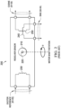
- FIG. 2 is a schematic diagram of a resolver sensor.
- Resolver sensor 200 is a resolver sensor such as resolver sensor 140 and is usually integrated with a motor 210.
- the resolver sensor 200 includes exciter reference (input) terminals R1 and R2, sine (output) terminals S2 and S4, and cosine (output) terminals S1 and S3.
- the resolver sensor 200 is arranged to generate, in response to an exciter reference signal (e.g., via terminals R1 and R2), a first output signal (e.g., via S2 and S4) and a second output signal (e.g., via S1 and S3).
- the generated first and second output signals are analog output signals for conveying rotation information for determining a rotation (including a position and/or speed) of the motor shaft 220 of motor 210.
- the resolver sensor 200 is an angular position sensor, which is commonly used in harsh, rugged environments.
- a fully electric vehicle (EV) or industry robots usually use one or more resolver sensors 200 for a variety of control systems that perform rotary and/or angular motion.
- a resolver-to-digital converter (RDC) interface processes the analog output signals output by the resolver sensor 200 and converts the rotation information of the analog output signals to a digital format.
- the digitally formatted rotation information is communicated, such as to the engine control unit (ECU) in an EV or to other micro-controllers/microprocessors in certain industrial robots control systems where determination of the angular position and/or velocity of the motor shaft 220 is required for normal processing.
- ECU engine control unit
- micro-controllers/microprocessors in certain industrial robots control systems where determination of the angular position and/or velocity of the motor shaft 220 is required for normal processing.
- the resolver sensor 200 is mechanically affixed on the motor shaft 220 of the motor 210, for which both relative and absolute angular position for the motor shaft 220 are to be continuously determined.
- the resolver sensor 200 is embodied as a rotating autotransformer having one rotor winding (e.g., coil 230), which is driven by an exciter sine wave via terminals R1 and R2.
- the rotor winding 230 is arranged about the motor shaft 220, which accordingly rotates as the motor 210 is running (e.g., "spinning").
- the resolver sensor 200 also includes two secondary windings (coils 240 and 250) that are mechanically placed 90 degrees apart (other phase angle placements are possible, such as 120 degrees for a 3-phase resolver sensor).
- the secondary coils 240 and 250 are coupled respectively to sine (S2 and S4) and the cosine (S1 and S3) terminals.
- the exciter signal applied to the primary coil is AC-coupled (e.g., inductively coupled) to the two stator windings.
- the rotor position angle ( ⁇ ) changes with respect to the stator windings.
- the rotor and stator windings have a turn ratio around the order of 30 percent.
- Resolver sensor 200 output signals are normally "gained” (e.g., selectively amplified), demodulated, and post-processed to extract angle and velocity information related to the motor shaft 220.
- FIG. 3 is a waveform diagram 300 of an exciter reference signal and the first and second output signals received from the resolver sensor 200.
- the exciter reference signal 330 is a double-ended (e.g., differential) signal generated by the resolver applied to the resolver sensor 200.
- the exciter reference signal 330 is generated by resolver 138 waveform generation circuitry and applied across the R1 and R2 terminals of the resolver sensor 200.
- the exciter reference signal 330 has a waveform in accordance with the equation sin(2 ⁇ ⁇ fc ⁇ t ) + a where fc is the excitation frequency, a is the common-mode amplitude (which is a constant), and t is time.
- the first (e.g., cosine) output signal 310 is a double-ended signal generated by the resolver sensor in response to inductive coupling of the exciter reference signal 330 from the (rotor) coil 230 to the second (stator) coil 250.
- the generated first output signal 310 is coupled across the S1 and S3 terminals of the resolver sensor 200.
- the resolver sensor 200 generates first (e.g., cosine) output signal 310 having a first sinusoidal envelope 312 in accordance with the equation sin(2 ⁇ ⁇ P ⁇ N / 60 ⁇ t ) where P indicates a number of poles of resolver sensor 200, N indicates the rpm (rotations per minute), and t is time.
- the second (e.g., sine) output signal 320 is a double-ended signal generated by the resolver sensor in response to inductive coupling of the exciter reference signal 330 from the (rotor) coil 230 to the first (stator) coil 240.
- the generated second output signal 320 is coupled across the S2 and S4 terminals of the resolver sensor 200.
- the resolver sensor 200 generates second (e.g., sine) output signal 320 having a second sinusoidal envelope 322 in accordance with the equation sin(2 ⁇ ⁇ P ⁇ N /60 ⁇ t ) where P indicates a number of poles of resolver sensor 200, N indicates the rpm (rotations per minute), and t is time.
- the angle ( ⁇ ) of the motor rotation can be determined by evaluating the arc-tangent function of the result of dividing the first sinusoidal envelope 322 divided by the instantaneous value by the second sinusoidal envelope 312.
- FIG. 4 is a high-level diagram of an architecture of a digital feedback loop tracking resolver.
- the digital feedback loop tracking resolver 400 includes an analog front end 410 (which includes differential input buffers 420 and 422, multipliers 430 and 432 and a differential comparator 440), digital blocks (which include the demodulator 450, the "type II" control loop 460 (e.g., having two "poles"-one at the origin-and one "zero,” where the zero is located between the two poles: such a compensation network helps shape the profile of the gain with respect to frequency while also providing a 90° phase boost), and the memory sine/cosine lookup table 470, and the digital-to-analog converters (DACs) 480 and 482.
- analog front end 410 which includes differential input buffers 420 and 422, multipliers 430 and 432 and a differential comparator 440
- digital blocks which include the demodulator 450, the "type II" control loop 460 (e.g., having two "poles"-one at
- the analog front end 410 is arranged to convert (e.g., via the differential input buffers 420 and 422) the sine and cosine differential input signals into respective "single-ended" signals given by equations (1) and (2) respectively:
- the amplitude-modulated resolver output signals of equation (1) and (2) are fed as the inputs to the digital feedback loop tracking resolver 400.
- a purpose of the digital feedback loop tracking resolver 400 loop is to calculate the angle ( ⁇ ) and velocity of the motor shaft. As indicated by FIG. 3 , the positioning information is conveyed via the envelope of the input sine and cosine signals. To calculate the conveyed angle, sine ⁇ is multiplied by a feedback signal (cosine ⁇ from DAC 480) where phi( ⁇ ) is the assumed angle resulting from the lookup table stored in memory. Similarly, cosine ⁇ is multiplied by the feedback signal (sine ⁇ from DAC 482).
- the output of the differential comparator 440 is digital and is demodulated by demodulator 450 to remove the carrier wave sin( ⁇ ⁇ t).
- the demodulator 450 To determine the carrier wave sin( ⁇ ⁇ t) information, the demodulator 450 generates the error signal V ⁇ ERR in response to the exciter reference signal.
- the error signal V ⁇ ERR is applied to the type-II (digital tracking) control loop 460 to convert the error signal V ⁇ ERR into an output signal for indicating the angle and velocity:
- V ⁇ ERR K ⁇ sin w ⁇ t ⁇ ⁇ ⁇ ⁇
- Negative feedback of the control loop configuration employed in the digital feedback loop tracking resolver architecture helps to continuously reduce the V ⁇ ERR signal to a value substantially close to zero.
- V ⁇ ERR the value of V ⁇ ERR is near zero.
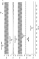
- FIG. 5 is a waveform diagram 500 of ideal first and second output signals received from a resolver sensor in accordance with example embodiments.
- the waveform diagram 500 includes an ideal first (cosine) output signal 510 received from an ideal resolver sensor, an ideal second (sine) output signal 520 received from an ideal resolver sensor, an ideal exciter reference signal 530 applied to the ideal resolver sensor, a first (e.g., longer window) voltage RMS (root mean square) output 540, a second (e.g., shorter window) voltage RMS output 542, and a fault signal 550 (e.g., for indicating when the first and second RMS output voltages deviate).
- the fault signal 550 is generated by the described resolver 138 and is described hereinbelow with reference to FIG. 16 .
- the voltage peak-to-peak (Vpk-pk) 502 of the ideal first (cosine) output signal 510 and the Vpk-pk 504 ideal second (sine) output signal 520, being ideal, are identical even though the respective peak-to-peak voltage of each such signal occurs at different times (e.g., phase offset and motor rotation speed).
- respective peak-to-peak voltages of the first (cosine) output signal 510 occurs when the phase angle is near 0°, 180°, 360°, and the like
- the peak-to-peak voltages of the second (sine) output signal 520 occurs when the phase angle is near 90°, 270°, and the like.
- the peak-to-peak voltages normally occur near (rather than exactly on) a selected phase angle because the peak-to-peak voltages are normally generated in accordance with the instantaneous orientation of the motor shaft and speed.
- the ideal first (cosine) output signal 510 and the ideal second (sine) output signal 520 are both ideal, the first (e.g., longer window) voltage RMS (root mean square) output 540 and the second (e.g., shorter window) voltage RMS output 542 are also ideal.
- both the first (e.g., longer window) voltage RMS output 540 and the second (e.g., shorter window) voltage RMS output 542 are the RMS of the ideal voltage peak-to-peak.
- the fault signal (e.g., for indicating when the first and second RMS output voltages deviate) is held to an un-asserted (logic zero) value.
- FIG. 6 is a waveform diagram 600 of finer details of ideal first and second output signals received from a resolver sensor in accordance with example embodiments.
- the waveform diagram 600 includes an ideal first (cosine) output signal 610, an ideal second (sine) output signal 620, an ideal exciter reference signal 630, a first (e.g., longer window) voltage RMS output 640, a second (e.g., shorter window) voltage RMS output 642, and a fault signal 650.
- each individual (e.g., sinewave) oscillation of the ideal first (cosine) output signal 610 and the ideal second (sine) output signal 620 generally can be perceived.
- peak-to-peak voltages of the ideal first (cosine) output signal 610 approach a maximum value around time 100 mS (e.g., when the cosine phase angle is near 0°).
- the peak-to-peak voltages of the second (sine) output signal 620 approach a minimum value (e.g., zero) around time 100 mS (e.g., when the sine phase angle is near 0°).
- FIG. 7 is a waveform diagram 700 of even finer details of ideal first and second output signals received from a resolver sensor in accordance with example embodiments.
- the waveform diagram 700 includes an ideal first (cosine) output signal 710, an ideal second (sine) output signal 720, an ideal exciter reference signal 730, a first (e.g., longer window) voltage RMS output 740, a second (e.g., shorter window) voltage RMS output 742, and a fault signal 750.
- each individual (e.g., sinewave) oscillation of the ideal first (cosine) output signal 710 and the ideal second (sine) output signal 720 is generally discernable.
- peak-to-peak voltages of the ideal first (cosine) output signal 710 approach a maximum value around time 100 mS (e.g., when the cosine phase angle is near 0°).
- peak-to-peak voltages of the second (sine) output signal 720 approach a minimum value (e.g., zero) around time 100 mS (e.g., having a generally flat-like appearance around time 100 mS).
- FIG. 8 is a waveform diagram 800 of fine details of ideal first and second output signals received from a resolver sensor at a different time in accordance with example embodiments.
- the waveform diagram 800 includes an ideal first (cosine) output signal 810, an ideal second (sine) output signal 820, an ideal exciter reference signal 830, a first (e.g., longer window) voltage RMS output 840, a second (e.g., shorter window) voltage RMS output 842, and a fault signal 850.
- each individual (e.g., sinusoidal) oscillation of the ideal first (cosine) output signal 810 and the ideal second (sine) output signal 820 is generally discernable.
- peak-to-peak voltages of the ideal first (cosine) output signal 810 approach a minimum value (e.g., zero) around time 124.8 mS (e.g., when the phase angle is near 90°).
- the peak-to-peak voltages of the second (sine) output signal 820 approaches a maximum value around time 124.8 mS (e.g., when the phase angle is near 90°).
- the maximum peaks of the ideal first (cosine) output signal and the ideal second (sine) output signal occur at different intervals.
- the spacing of such intervals is dependent upon the rotational speed of the motor being monitored by a described resolver.
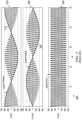
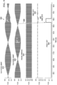
- FIG. 9 is a waveform diagram 900 of imbalanced first and second output signals received from a resolver sensor in accordance with example embodiments.
- the waveform diagram 900 includes a (e.g., degraded) first (cosine) output signal 910, a second (sine) output signal 920, an exciter reference signal 930, a first (e.g., longer window) voltage RMS output 940, a second (e.g., shorter window) voltage RMS output 942, and a fault signal 950.
- the first (cosine) output signal 910 is non-ideal, such as a result of noise being injected into the resolver sensor at around a time of 155 mS.
- the noise can result from the motor itself (which in many common electric vehicles can consume around 10 - 40 amps of current) and/or control circuitry (e.g., for selectively powering motive windings of the motor coil).
- common mode rejection of resolver system 138 e.g., which is inherent to the differential signals
- conventional resolver systems can make a substantially incorrect angle determination (e.g., depending on the degree of the disproportionality and the tolerances of a particular application).
- the first (cosine) output signal 910 can be non-ideal, such as a result of a defect in the resolver sensor generating the output signal received from a resolver sensor.
- Resolver sensors usually include multiple poles and/or windings. When adjacent portions of insulation of individual turns are comprised, individual turns having adjacent, compromised insulation can be shorted (e.g., directly or indirectly). When the shorted turns occur in a winding, the shorted turns result in the winding causing a dip in amplitude of an output signal of the resolver sensor.
- the dip 902 (e.g., with respect to Vpk-pk 904) in amplitude reduces the angular accuracy of conventional resolver systems, and the stability (e.g., "lock") of resolver feedback loop could be broken (such as depending, on the tolerances of a particular application).
- the disproportionality of the effect(s) of noise or faulty windings or other mechanical imperfections in the resolver sensor causes an imbalance, which potentially can result in incorrect shaft angle readings and/or destabilized feedback control loops.
- the imbalance is detected as a function of comparing and thresholding (e.g., see comparators 1662 and 1664 described hereinbelow) the first (e.g., longer window) voltage RMS output 940 and the second (e.g., shorter window) voltage RMS output 942.
- the resolver asserts the fault signal 950 around the time of 155 mS.
- FIG. 10 is a waveform diagram 1000 of finer details of imbalanced first and second output signals received from a resolver sensor in accordance with example embodiments.
- the waveform diagram 1000 includes a (e.g., degraded) first (cosine) output signal 1010, a second (sine) output signal 1020, an exciter reference signal 1030, a first (e.g., longer window) voltage RMS output 1040, a second (e.g., shorter window) voltage RMS output 1042, and a fault signal 1050.
- noise and/or a winding fault causes a drop 1002 in the instantaneous peak-to-peak voltage of the first (e.g., cosine) voltage output signal 1010.
- the described resolver 138 generates the first (e.g., longer window) voltage RMS output 1040 in response to integrating the first (e.g., cosine) voltage output signal 1010 and the second (e.g., sine) voltage output signal over a longer window (e.g., 20-times longer than the shorter window).
- the described resolver 138 generates the second (e.g., shorter window) voltage RMS output 1042 in response to integrating the first (e.g., cosine) voltage output signal 1010 and the second (e.g., sine) voltage output signal 1020 over a shorter window (e.g., 20-times shorter than the shorter window).
- a shorter window e.g. 20-times shorter than the shorter window.
- the value of the second (e.g., shorter window) voltage RMS output 1042 falls (more quickly than the RMS output 1040) in response to the drop 1002 in the peak-to-peak voltage of the first (e.g., cosine) voltage output signal 1010.
- the lowered value of the second (e.g., shorter window) voltage RMS output 1040 is discernable near time 155, where the (e.g., power) value of the second (e.g., shorter window) voltage RMS output 1042 diverges (e.g., becomes less than) the corresponding value of the first (e.g., longer window) voltage RMS output 1040.
- the resolver 138 asserts (e.g., 1004) the fault signal 1050 around the time of 155 mS.
- the rotation of the motor shaft causes the instantaneous peak-to-peak voltage of the first (e.g., cosine) voltage output signal 1010 to (e.g., gradually) rise to a normal (e.g., non-error) value.
- the resolver 138 deasserts the fault signal 1050 around the time of 161 mS.
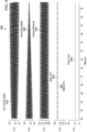
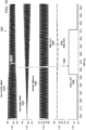
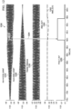
- FIG. 11 is a waveform diagram 1100 of multiple imbalanced first and second output signals received from a resolver sensor in accordance with example embodiments.
- the waveform diagram 1100 includes a (degraded) first (cosine) output signal 1110, a second (sine) output signal 1120, an exciter reference signal 1130, a first (e.g., longer window) voltage RMS output 1140, a second (e.g., shorter window) voltage RMS output 1142, and a fault signal 1150.
- noise and/or a winding fault causes a drop 1102 in the instantaneous peak-to-peak voltage of the first (e.g., cosine) voltage output signal 1110.
- the described resolver 138 generates the first (e.g., longer window) voltage RMS output 1140 in response to integrating the first (e.g., cosine) voltage output signal 1110 and the second (e.g., sine) voltage output signal over a longer window (e.g., 20-times longer than the shorter window).
- the described resolver 138 generates the second (e.g., shorter window) voltage RMS output 1142 in response to integrating the first (e.g., cosine) voltage output signal 1110 and the second (e.g., sine) voltage output signal 1120 over a shorter window (e.g., 20-times shorter than the shorter window).
- a shorter window e.g. 20-times shorter than the shorter window.
- the value of the second (e.g., shorter window) voltage RMS output 1142 falls (more quickly than the RMS output 1140) in response to the drop 1102 in the peak-to-peak voltage of the first (e.g., cosine) voltage output signal 1110.
- the lowered value of the second (e.g., shorter window) voltage RMS output 1140 is discernable near time 192 mS, where the (e.g., power) value of the second (e.g., shorter window) voltage RMS output 1142 diverges (e.g., becomes less than) the corresponding value of the first (e.g., longer window) voltage RMS output 1140.
- the resolver 138 deasserts the fault signal 1150 around the time of 197 mS.
- Additional imbalances are detected and handled by the described resolver 138 in a similar manner (e.g., to the imbalance starting at time 155 mS). For example, a fault imbalance is detected at around times 192 mS, 204 mS, and 211 mS, where the fault signal 1150 is respectively asserted (e.g. 1104) for each such time, and the fault signal 1150 is respectively deasserted at around times 197 mS, 209 mS, and 214 mS (where the each imbalance is reduced to a level within a thresholded tolerance range).
- FIG. 12 is a waveform diagram 1200 of fine details of imbalanced first and second output signals received from a resolver sensor in accordance with example embodiments.
- the waveform diagram 1200 includes a (non-ideal) first (cosine) output signal 1210, a second (sine) output signal 1220, an exciter reference signal 1230, a first (e.g., longer window) voltage RMS output 1240, a second (e.g., shorter window) voltage RMS output 1242, and a fault signal 1250.
- a rotationally dependent (e.g., winding- or noise-induced fault that is functionally dependent on a shaft angle) fault causes a drop in the instantaneous peak-to-peak voltage of the first (e.g., cosine) voltage output signal 1210.
- the described resolver 138 generates the first (e.g., longer window) voltage RMS output 1240 in response to integrating the first (e.g., cosine) voltage output signal 1210 and the second (e.g., sine) voltage output signal over a longer window (e.g., 20-times longer than the shorter window).
- the described resolver 138 generates the second (e.g., shorter window) voltage RMS output 1242 in response to integrating the first (e.g., cosine) voltage output signal 1210 and the second (e.g., sine) voltage output signal 1220 over a shorter window (e.g., 20-times shorter than the shorter window).
- a shorter window e.g. 20-times shorter than the shorter window.
- the value of the second (e.g., shorter window) voltage RMS output 1240 falls in response to the drop 1202 in the peak-to-peak voltage of the first (e.g., cosine) voltage output signal 1210.
- the resolver 138 asserts (e.g., 1204) the fault signal 1250 around the time of 192 mS.
- the resolver 138 deasserts the fault signal 1250 around the time of 197 mS.
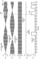
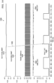
- FIG. 13 is a waveform diagram 1300 of imbalanced first and second output signals received from a resolver sensor of a static motor in accordance with example embodiments.
- the waveform diagram 1300 includes a (e.g., degraded) first (cosine) output signal 1310, a second (sine) output signal 1320, an exciter reference signal 1330, a first (e.g., longer window) voltage RMS output 1340, a second (e.g., shorter window) voltage RMS output 1342, and a fault signal 1350.
- a non-rotationally dependent fault causes a rise in the voltage of the first (e.g., "cosine") voltage output signal 1310.
- the value of the second (e.g., shorter window) voltage RMS output 1340 rises in response to the rise in the voltage of the first (e.g., "cosine") voltage output signal 1310.
- the resolver 138 asserts (e.g., 1302) the fault signal 1350 around the time of 330 mS.
- the resolver 138 deasserts the fault signal 1350 around the time of 335 mS.
- FIG. 14 is a waveform diagram 1400 of subsequent imbalanced first and second output signals received from a resolver sensor of a static motor in accordance with example embodiments.
- the waveform diagram 1400 includes a (degraded) first (cosine) output signal 1410, a second (sine) output signal 1420, an exciter reference signal 1430, a first (e.g., longer window) voltage RMS output 1440, a second (e.g., shorter window) voltage RMS output 1442, and a fault signal 140.
- a non-rotationally dependent fault causes a rise in the voltage of the first (e.g., "cosine") voltage output signal 1410.
- the value of the second (e.g., shorter window) voltage RMS output 1440 rises in response to the rise in the voltage of the first (e.g., cosine) voltage output signal 1410.
- the resolver 148 asserts (e.g., 1402) the fault signal 1450 around the time of 396 mS.
- the resolver 148 deasserts the fault signal 1450 around the time of 401 mS.
- FIG. 15 is a schematic diagram of a resolver sensor output signal power averaging circuit 1500.
- the resolver sensor output signal power averaging circuit 1500 includes "square" (e.g., as in performing the mathematic exponential squaring function) cells 1510, 1520, and 1530, current summer 1540, and integrator (e.g., capacitor) C15.
- the resolver signal output signal power averaging circuit 1500 is arranged to generate an average power signal for indicating an average value of the resolver sensor output signal power, where the average is determined in response to a time window determined in response to the value of C15.
- the resolver sensor output signals are signals, such as the first (e.g., cosine) output signal V in1 and the second (e.g., sine) output signal V in2 .
- the square cell 1510 is arranged to square an average of the first (e.g., cosine) output signal V in1 , with respect to common mode signal V COM such that a first current is generated for representing the first squared average (power).
- the square cell 1520 is arranged to square an average of the second (e.g., sine) output signal V in2 , with respect to common mode signal V COM such that a second current is generated for representing the second squared average (power).
- the square cell 1530 is arranged to square the average of average power signal V C and the common mode signal V COM such that a third current is generated for representing the third squared average (power).
- Each of the generated (e.g., first, second, and third) currents is summed (e.g., added or subtracted) by current summer 1540 to produce a summed current 1546, which generates the average power signal V C in accordance with the voltage developed by an averaging capacitor C (e.g., integrator C15). Accordingly, the average power signal V C establishes (e.g., is a portion of) a feedback loop, where current added by the square cells 1510 and 1520 is offset (e.g., in a stable and locked steady state operation condition) by the current subtracted by the square cell 1530.
- V C t V C t 0 + 1 C ⁇ t 0 t i V 1 cos ⁇ sin ⁇ t + i V 2 sin ⁇ sin ⁇ t ⁇ I
- Vc dt 8 V C t 0 + k C ⁇ t 0 t 0 + T V 1 cos ⁇ sin ⁇ t 2 + V 2 sin ⁇ sin ⁇ t 2 ⁇ V C t 2 dt 9
- k is a constant and t is a particular time between t 0 (an initial time) and T (elapsed time after t 0 ).
- the integration term of equation (9) is set equal to zero.
- V C t 2 T ⁇ t 0 t 0 + T V 1 cos ⁇ sin ⁇ t 2 + V 2 sin ⁇ sin ⁇ t 2 dt
- the sin( ⁇ t) effect is decoupled by the squared-sum calculation (such that, as described herein, errors can be detected in the V in1 and V in2 signals independently of a reference to oscillations of an excitation signal).
- the power term V RMS of equation (13) is independent of the coefficient k/C in equation (9). However, the coefficient k/C determines the time window (e.g., settling time) over which the power term V RMS is determined.
- resolver sensor output signal power averaging circuits 1500 each including different-valued integrators C15 are described for producing average power calculations using shorter and longer time windows (as described hereinbelow with reference to FIG. 16 ).
- V in1 and V in2 signals are degraded by any of offset drift, distortion, winding faults, "glitches,” and coupled noise, the V RMS is affected (e.g., changed), and such changes in V RMS that exceed a selected threshold can be detected by the resolver output signal power imbalance detector described hereinbelow with reference to FIG. 16 .
- the square cell 1530 can be omitted and can be replaced by an optional switch S15.
- the switch S15 is arranged to selectively set (e.g., during a steady-state operating condition) the integrator C15 to a known voltage (e.g., in response to a signal "discharge" asserted by a processor controlling programmable components of the resolver sensor output signal power averaging circuit 1500).
- a processor controlling programmable components of the resolver sensor output signal power averaging circuit 1500.
- a square cell such as 1530 can be arranged to subtract current at a summing node, and/or current can be subtracted by selectively using a switch S15 to discharge the averaging capacitor C15.
- the voltage developed at the high side of the averaging capacitor C15 is accordingly controlled such that the developed voltage is normally within the operational voltage range of the comparators 1662 and 1664 described hereinbelow.
- average power signal are generated for detecting a power imbalance between the first and second resolver sensor output signals.
- the first and second resolver sensor output signals are usually generated by a resolver sensor in response to inductively coupling an exciter reference signal such that the first resolver sensor signal is associated with first physical orientation that is different from a second physical orientation associated with the second resolver sensor signal.
- a power imbalance e.g., which can be caused by a fault-causing transient condition such as electrical noise or a winding defect
- the power imbalance is detected and a fault signal is generated.
- the fault signal is used to "warn" control circuitry, such as warning that positioning (and/or rotational speed) information derived from the first and second resolver sensor output signals is degraded such that protective measures can be taken (including blocking actions by the control circuitry that might otherwise be taken).
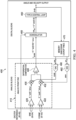
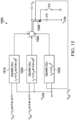
- FIG. 16 is a schematic diagram of a resolver sensor output signal power imbalance detector 1600 in accordance with an embodiment of the invention.
- the resolver sensor output signal power imbalance detector 1600 includes resolver output signal power averaging circuits 1602 and 1604, programmable voltage dividers 1654 and 1658, comparators 1662 and 1664, and fault signal generator 1670.
- the resolver output signal power averaging circuits 1602 and 1604 are arranged to each generate an average power signal in response to first and second resolver sensor output signals.
- Each of the generated average power signals is averaged using a different time period (e.g., window), such that a transient (such as the start of a transient due to noise or a winding defect) signal imposed on one of the first and second resolver sensor output signals affects the generated average power signals unevenly.
- the imbalanced first and second resolver sensor output signals affect the generated average power signals unevenly because of the different integration rates and/or different time windows of the resolver output signal power averaging circuits 1602 and 1604.
- the duration of the first and second time windows are selected to have a duration such that that an imbalance caused by a transient event is detectable by comparing a first average power signal with a second average power signal.
- the first average power signal is generated by the resolver output signal power averaging circuit 1602 and the second average power signal is generated by the resolver output signal power averaging circuit 1604. Accordingly, comparing the (e.g., differently affected) average power signals determines (e.g., within selected thresholds) an error condition caused by the power imbalance and a fault signal is generated in response for indication the error condition.
- the resolver sensor output signal power imbalance detector 1600 operates virtually completely in an analog domain. For example, substantially operating in the analog domain obviates costs associated with conventional digital solutions and digital signal processing.
- the described resolver sensor output signal power imbalance detector 1600 can be laid out relatively compactly.
- the square cell 1700 (which is representative of portions of square cells such as 1610, 1620, 1630, 1612, 1622, and 1632) is described hereinbelow with reference to FIG. 17 (e.g., in view of FIG. 16 ).
- the square cell 1700 includes analog components, which can be laid out compactly and also closely replicated such that each such replicated square cell performs substantially similarly with respect to PVT (process, voltage, and temperature) variations.
- the resolver output signal (longer term) power averaging circuit 1602 includes the square cells 1610, 1620, and 1630, current summer 1640, and integrator (e.g., capacitor) C16a.
- the first square cell 1610 is a circuit for generating a resolver sensor first output power signal (e.g., for indicating the power of the resolver sensor first output signal).
- the second square cell 1620 is a circuit for generating a resolver sensor second output power signal (e.g., for indicating the power of the resolver sensor second output signal).
- the third square cell 1630 is a circuit for a third square circuit for generating a first (e.g., longer term) average value of the resolver sensor output signal power and coupling the resolver sensor first output power signal to the current summer 1640.
- the current summer 1640 is a circuit for summing the resolver sensor first and second output power signals and the squared resolver sensor first output power signal, and coupling the summation to the integrator C16a.
- the resolver output signal power averaging circuit 1602 is arranged to generate a first average power signal for indicating an average value of the resolver output signal power, where the average is determined in response to a first time window determined in response to the value of integrator C16a.
- the resolver output signal (shorter-term) power averaging circuit 1604 includes the square cells 1612, 1622, and 1632, current summer 1642, and integrator (e.g., capacitor) C16b.
- the first square cell 1612 is a circuit for generating a resolver sensor first output power signal (e.g., for indicating the power of the resolver sensor first output signal).
- the second square cell 1622 is a circuit for generating a resolver sensor second output power signal (e.g., for indicating the power of the resolver sensor second output signal).
- the third square cell 1632 is a circuit for a third square circuit for generating a second (e.g., near instantaneous-term) average value of the resolver sensor output signal power and coupling the second average value of resolver output signal power to the current summer 1642.
- the current summer 1642 is a circuit for summing the resolver sensor first and second output power signals and coupling the summation to the integrator C16b.
- the resolver output signal power averaging circuit 1604 is arranged to generate a second average power signal for indicating a second average value of the resolver output signal power, wherein the second average value is determined in response to a second time window determined in response to the value of a second integrator.
- the second time window is selected to be shorter than the first time window such that the time window (e.g., having a time period determined by an integration rate of a respective integrator C16) is different between the resolver output signal power averaging circuit 1602 and the resolver output signal power averaging circuit 1604.
- Square cell 1610 is coupled to the same input signals as square cell 1612, and the square cell 1620 is coupled to the same input signals as square cell 1622.
- components of square cells having the same inputs can be shared (and, for example, current mirrors can be applied to the outputs, such that the output currents can be summed by separate summers, such as 1640 and 1642).
- Square cells 1630 and 1632 do not share common inputs (as described hereinbelow) and are usually laid out as separate square cells (when implemented).
- the resolver sensor output signal power imbalance detector 1600 can be laid out with only four square cells.
- a first square cell of the resolver output signal power averaging circuit 1602 and a first square cell of the resolver output signal power averaging circuit 1604 share a reference current mirror for generating separate output signals in response to a first set of common inputs (e.g., a first resolver sensor output signal and a feedback signal).
- a second square cell of the resolver output signal power averaging circuit 1602 and a second square cell of the resolver output signal power averaging circuit 1604 share a reference current mirror for generating separate output signals in response to a second set of common inputs.
- the operation of the resolver output signal power averaging circuits 1602 and 1604 is generally similar to the operation of resolver output signal power averaging circuits 1500 described hereinabove.
- the averaging capacitor C16a (of signal power averaging circuit 1602) is a different value than the averaging capacitor C16b (of signal power averaging circuit 1604).
- the difference in size between capacitors C16a and C16b causes voltages to be developed at different rates for nodes V C1 and V C2 , such that different currents are developed by the square cells 1630 and 1632 (as described hereinabove with respect to FIG. 15 ). Accordingly, the amount of current supplied by square cell 1630 to the current summer 1640 is different from the amount of current supplied by square cell 1632 to the current summer 1642.
- the averaging time (e.g., RMS measurement window) of node V C1 is proportionately larger than the averaging time of nodes V C2 . Accordingly, the voltage of node V C2 is associated with input signal power measured over a shorter-term (e.g., relatively instantaneous) RMS measurement window, is associated with input signal power measured over a longer-term RMS measurement window.
- the shorter-term RMS measurement window is selected to be short enough such that a phase imbalance can be detected within a relatively short period of time (e.g., within a period less than around two or more oscillations and/or within a period less than around one-half of the longer-term RMS measurement window).
- the shorter-term RMS measurement window is selected to be (e.g., slightly) than a selected EMI/noise time period, such that the shorter window excludes disturbances in the measured power caused by EMI, noise, winding faults, and similar causes (e.g., collectively, "noise"). Accordingly, the length of the shorter-term RMS measurement window is determined in response to a selected noise time period.
- the selected noise time period can be selected, such as by empirically measuring and/or observing noise in one or more systems and selecting a value by which many (and perhaps most or all) events causing noise are not detected by the shorter window (and still remain detectable using the longer-term RMS measurement window).
- V C2 When one the input signals is suddenly corrupted, the nearly instantaneous power RMS value V C2 responds more quickly than does longer-term average counterpart V C1 , such that a fault is triggered when the difference exceeds a selected (e.g., programmable) voltage threshold.
- the selected voltage threshold is selected (e.g., programmed) to level in accordance with closing (e.g., actuated under software control of a processor controlling programmable components of the resolver sensor output signal power imbalance detector 1600) selected switches in first and second programmable voltage dividers (1654 and 1658), in accordance with the amount of currents sourced and sunk by (e.g., bandgap circuit) current sources, and in accordance with resistor network theory.
- each of the individual resistors in the programmable voltage dividers 1654 and 1658 are selected (e.g., at design time) to provide programmable levels to provide different sensitivity levels (e.g., after deployment) for different (and, e.g., expected) motor applications.
- the programmable levels can be selected in accordance with Ib*R*N, where Ib is a current generated responsive to a bandgap reference and R is a resistance selected in accordance with selected switching configuration N and the values of the resistors selected by the selected switching configuration.
- the value N can be a hexadecimal value, where each bit selects the state of a switch for selectively coupling an individual resistor to a selected resistor network configuration.
- the fault signal generator 1670 is arranged to toggle (e.g., assert and deassert) the fault signal output in response to the thresholding and comparisons of comparators 1662 and 1664 (collectively, “comparator circuit").
- the comparator circuit is arranged to compare the first average power signal and the second average power signal and to generate (via fault signal generator 1670) a fault signal when the first average power signal and the second average power signal differ by the threshold voltage.
- the comparator 1662 toggles high (e.g., is set to logic one) when the instantaneous (e.g., shorter-term) average power is greater than the longer-term power average power by the programmed voltage threshold.
- the comparator 1664 toggles high (e.g., is set to logic one) when the instantaneous (e.g., shorter-term) average power is less than the longer-term power average power by the programmed voltage threshold.
- the fault signal generator 1670 is arranged to assert the fault signal output when either of the comparators 1662 and 1664 is toggled high, and to deassert the fault signal output when both of the comparators 1662 and 1664 are toggled low.
- the voltage threshold can be embodied as an (e.g., hysteretic) offset within a comparator such that (e.g., a portion of) the threshold is fixed and "designed-in" to the comparator.
- the programmable voltage dividers 1654 and 1658 can be omitted or combined with a comparator circuit having a designed-in offset for a voltage threshold.
- FIG. 17 is a schematic diagram of a square cell.
- the square cell 1700 is a square cell such as described in United States Pat. No. 7,791,400 .
- the square cell 1700 includes a voltage divider 1710, and amplifier 1720, a "head” current mirror 1730, and a "tail” current mirror 1740.
- the voltage divider 1710 is arranged to scale an input voltage (e.g., V in1 ) to a voltage suitable for biasing the input transistor MN1 of the amplifier 1720.
- the amplifier 1720 is arranged to output a current having a magnitude in accordance with a square of a scaled input voltage.
- the transistor MN1 performs the square calculation, where any current injection from MN1 to node N1 raises the voltage of node N1 such that the voltage rise in N1 is amplified by transistor MN0 at node N2, which in turn raises the gate voltage of transistor MN2 (of tail current mirror 1740) such that the transistor MN2 is arranged to sink the current injected into node N1.
- the "tail” current mirror 1740 can be arranged with additional mirrored output transistors, such that multiple duplicate outputs of the "squared" current are provided (e.g., where each mirrored output is for separately controlling the charging and discharging of one of the averaging capacitors C16a and C16b described hereinabove with reference to FIG. 16 ).
- more than two modulated signals received from the resolver sensor 140 can be monitored for imbalance detection in accordance with the description herein.
- the ⁇ effect e.g., sinusoidal exciter reference stimulus
- a three-phase resolver is arranged to operate in accordance with three electrical phases, each having a phase offset of 120 degrees from an adjacent coil.
- the three-phase resolver secondary coils generate an electromagnetic field in response to an exciter reference signal.
- Three stator coils are positioned, (e.g., 120 degrees apart from an adjacent coil with respect to a longitudinal axis of the shaft.
- equation (14) the sine effect of the first, second, and third resolver output signals is decoupled from the power term.
- the energy indicated by equation (14) is 50 percent more than the power term V RMS of equation (13).
- an additional square cell is instantiated (not shown in the drawing). Accordingly, three square cells for each of V1, V2 and, V3 are provided, and two Vc1 and Vc2 square cells are provided as described hereinabove.
- the additional power is (normally) applied to both a longer-term first power averaging circuit and a shorter-term second power averaging circuit, such that the V C(t) terms are integrated at different rates (e.g., using different time windows). Because the fault signal is generated on the basis of the comparison, no fault is detected in a balanced condition because the additional power is applied equally to both power averaging circuits.
- the combined power output is also in accordance with equation (14) in part due to trigonometric identities. Accordingly, the exciter signal sine function can be decoupled from a power output signal using any suitable trigonometric functions (where the decoupled power output signal can be used in an analog domain to determine an imbalance in the output signals of an angular resolver).
- each of the stator coils output an (e.g., differential) resolver output signal.
- Each of the three resolver output signals is coupled to a first (longer-term) power averaging circuit such that a current representing the square of the voltage is generated.
- each of the three resolver output signals is coupled to a second (shorter-term) power averaging circuit such that a current representing the square of the voltage is generated (as described hereinabove, current mirrors can be used where different outputs are generated from a same set of inputs).
- a comparator circuit is arranged to compare the first average power signal and the second average power signal and generates a fault signal when the first average power signal and the second average power signal differ by a voltage threshold.
Description
- Computers (including processors) are increasingly used to control the movement of physical devices such as motors and robots. The computers control the movement of such physical devices in response to positioning (including speed) information received from sensors. The information from the sensors is often conveyed as one or more electrical signals. However, the sensors are often located in electrically noisy environments (such as a gasoline-engine compartment) where components such as switches and coils generate substantial amounts of electromagnetic interference, which typically degrades the quality and resolution of the conveyed electrical signals. The degraded electrical signals limit the speeds and/or accuracy of the controlled attributes (such as motor speeds and angular displacement) of the controlled physical devices, which normally limits the degree to which the computers can control a physical device.
US 6,205,009 describes a method for detecting fault in a resolver generating a sine voltage and a cosine voltage, whereby the sum of a square of the sine voltage and a square of the cosine voltage is obtained, and the sum is filtered through first and second filters to generate first and second filter outputs that are compared to detect a fault in the resolver. - According to the invention there is provided a circuit, a system, and a method for performing angular resolver imbalance detection, as set out in the appended claims.
-
-
FIG. 1 shows an illustrative electronic device in accordance with example embodiments. -
FIG. 2 is a schematic diagram of a resolver sensor. -
FIG. 3 is a waveform diagram 300 of an exciter reference signal and the first and second second output signals received from the resolver sensor. -
FIG. 4 is a high-level diagram of an architecture of a digital feedback loop tracking resolver. -
FIG. 5 is a waveform diagram 500 of ideal first and second output signals received from a resolver sensor in accordance with example embodiments. -
FIG. 6 is a waveform diagram 600 of finer details of ideal first and second output signals received from a resolver sensor in accordance with example embodiments. -
FIG. 7 is a waveform diagram 700 of even finer details of ideal first and second output signals received from a resolver sensor in accordance with example embodiments. -
FIG. 8 is a waveform diagram 800 of fine details of ideal first and second output signals received from a resolver sensor at a different time in accordance with example embodiments. -
FIG. 9 is a waveform diagram 900 of imbalanced first and second output signals received from a resolver sensor in accordance with example embodiments. -
FIG. 10 is a waveform diagram 1000 of finer details of imbalanced first and second output signals received from a resolver sensor in accordance with example embodiments. -
FIG. 11 is a waveform diagram 1100 of multiple imbalanced first and second output signals received from a resolver sensor in accordance with example embodiments. -
FIG. 12 is a waveform diagram 1200 of fine details of imbalanced first and second output signals received from a resolver sensor in accordance with example embodiments. -
FIG. 13 is a waveform diagram 1300 of imbalanced first and second output signals received from a resolver sensor of a static motor in accordance with example embodiments. -
FIG. 14 is a waveform diagram 1400 of subsequent imbalanced first and second output signals received from a resolver sensor of a static motor in accordance with example embodiments. -
FIG. 15 is a schematic diagram of a resolver sensor output signalpower averaging circuit 1500. -
FIG. 16 is a schematic diagram of a resolver sensor output signalpower imbalance detector 1600 in accordance with an embodiment of the invention. -
FIG. 17 is a schematic diagram of a square cell. - In this description, a system can be a sub-system of yet another system. Also, in this description, the terms "coupled to" or "couples with" (and the like) describe either an indirect or direct electrical connection. Thus, if a first device couples to a second device, that connection can be made through a direct electrical connection, or through an indirect electrical connection via other devices and connections. Further, in this description, the term "portion" can mean an entire portion or a portion that is less than the entire portion.
-
FIG. 1 shows anillustrative computing device 100 in accordance with example embodiments. For example, thecomputing device 100 is, or is incorporated into, anelectronic system 129, such as a computer, electronics control "box" or module, robotics equipment (including fixed or mobile), automobiles or any other type of system where a computer controls physical devices. - In some embodiments, the
computing device 100 comprises a megacell or a system-on-chip (SoC) which includes control logic components such as a CPU 112 (Central Processing Unit), a storage 114 (e.g., random access memory (RAM)) and apower supply 110. For example, theCPU 112 can be a CISC-type (complex instruction set computer) CPU, RISC-type CPU (reduced instruction set computer), MCU-type (microcontroller unit), or a digital signal processor (DSP). TheCPU 112 includes functionality provided by discrete logic components and/or is arranged to execute application-specific instructions (e.g., software or firmware) that, when executed by theCPU 112, transform theCPU 112 into a special-purpose machine. The notional line of "division" between hardware and software is a design choice that (e.g., selectively) varies depending on various tradeoffs including cost, power dissipation, reliability, and time to market. Accordingly, the functionality of any software used to control one ormore CPUs 112 of thecomputing system 100 can be entirely embodied as hardware (e.g., when given sufficient time and resources for design and manufacture). - The storage 114 (which can be memory, such as on-processor cache, off-processor cache, RAM, flash memory, data registers, flip-flops, and disk storage) stores one or more software applications 130 (e.g., embedded applications) that, when executed by the
CPU 112, transform thecomputing device 100 into a special-purpose machine suitable for performing a targeted function such as angular resolver imbalance detection. - The
CPU 112 comprises memory and logic that store information frequently accessed (e.g., written to and/or read from) from thestorage 114. Thecomputing device 100 is often controlled by a user using a UI (user interface) 116, which provides output to and receives input from the user during the execution thesoftware application 130. The output is provided using thedisplay 118, which includes annunciators (such as indicator lights, speakers, and vibrators) and controllers. The input is received using audio and/or video inputs (such as using voice or image recognition), and electrical and/or mechanical devices (such as keypads, switches, proximity detectors, gyros, accelerometers, and resolvers). - The
CPU 112 is coupled to I/O (input-output)port 128, which provides an interface that is configured to receive input from (and/or provide output to) networkeddevices 131. Thenetworked devices 131 can include any device (including "Bluetooth" units that are electronically paired with the computing device 100) capable of point-to-point and/or networked communications with thecomputing device 100. Thecomputing device 100 is optionally coupled to peripherals and/or computing devices, including tangible, non-transitory media (such as flash memory) and/or cabled or wireless media. These and other input and output devices are selectively coupled to thecomputing device 100 by external devices using wireless or cabled connections. Thestorage 114 is accessible, such as by thenetworked devices 131. TheCPU 112,storage 114, andpower supply 110 can be coupled to an external power supply (not shown) or coupled to a local power source (such as a battery, solar cell, alternator, inductive field, fuel cell, and capacitor). - The
computing system 100 includes aresolver 138 arranged to receive and evaluate electrical signals (which, for example, convey information) from aresolver sensor 140. As described hereinbelow, theresolver sensor 140 is arranged to generate and output (at least) first and second resolver sensor output signals for indicating a degree of rotation of a shaft. The first and second resolver sensor output signals are modulated signals, such as which correspond to the angular displacement or speed of a rotating shaft (such as the shaft of a motor). The modulated signals ideally have selected peak voltages and are offset by a constant phase angle. The phase angle is ideally around 90 degrees in a two-secondary coils-based resolver-based system, and ideally around 120 degrees in a three-secondary coils-based resolver-based system. Single-phase and other poly-phase systems are possible herein in accordance with this description and principles of motors and electromagnetism. - As described hereinbelow, a selected phase angle is determined by the number of resolver sensor secondary coils and the phase angle difference between the resolver sensor secondary coils. The selected phase angle is usually determined by the number of resolver sensor phase coils, which allows geometric principles to be applied such that frequencies of an exciter reference signal can be substantially removed (e.g., decoupled) from the modulated signals received from the
resolver sensor 140. Substantial removal includes reducing the modulated signals by around 70 percent, which corresponds to a phase angle error of 45 degrees, such that a phase angle of around 45 degrees or more in a two-phase system can be used to detect power imbalances. However, sufficiently high threshold levels (as described hereinbelow with reference toFIG. 16 ) are used to compensate for the remaining presence (e.g., ripple) of the exciter reference signal (e.g., oscillations) within an average power signal (generated in response to the modulated signals received from the resolver sensor 140). - The
resolver 138 evaluates the modulated signals received from theresolver sensor 140 to determine the angle and/or velocity of the motor shaft. Theresolver 138 also includes diagnostic circuitry to determine whether the received modulated signals are balanced (e.g., unaffected by electrical noise and/or winding defects). For example, the received modulated signal are balanced when the received modulated signals have peak voltages in accordance with selected peak voltages and/or are separated by the constant phase angle, such that an angle of rotation of a shaft (e.g., which contains a coil for inductively transmitting the exciter reference signal) can be resolved (e.g., determined). - When the received modulated signals are not balanced, errors in resolving the angle of rotation of the shaft can occur. To help minimize the possibility of generating control signals in response to erroneous information (and, for example, to increase speed and resolution of the resolver signal processing), the
resolver 138 is arranged to generate a fault signal indicating the received modulated signals are not balanced. The fault signal is usually coupled to a processor, such asCPU 112, such that the processor can take action to provide special handling (including ignoring) of the received modulated signals. - In an embodiment, the
resolver 138 receives sine/cosine modulated signals Vin1 and Vin2 (where Vin1=V1∗cos(θ)sin(ωt) and Vin2=V2∗sin(θ)sin(ωt)). The modulated signals are usually less than around 15 kHz, although in accordance with the description herein, the modulated signals Vin1 and Vin2 are not limited to frequencies of less than around 15 kHz, because of the described decoupling of the modulation frequencies. Theresolver 138 is arranged to resolve and convert the resolving angle θ of Vin1 and Vin2 into digital words (e.g., 10-bit or 12-bit words) representing motor angle and/or velocity (e.g., such that the speed and/or instantaneous position of the shaft can be conveyed). In the embodiment, the two input (e.g., enveloping) peak voltages of Vin1 and Vin2 should ideally be the same. Any deviation and/or imbalance between the input Vin1 and Vin2 signals (e.g., that exceeds a respective tolerance for offset, offset drift, distortion, glitch, and noise) is considered to cause errors in the resolving angle θ, and accordingly is reported as a fault (e.g., via the error signal). - However, comparing the peak and/or valley voltages between the Vin1 and Vin2 signals is not necessarily straightforward because the peak and valley voltages of each of the Vin1 and Vin2 signals occur at different times and depend on motor speed and position. In a first example, the nominal input signal amplitudes V1 and V2 (of Vin1 and Vin2, respectively), and offset drift, distortion, and noise are all amplitude-modulated by the term sin(ωt) in accordance with usual resolver sensor operation. When the shaft of the resolver motor spins very slowly or even stops, a fault can be generated. When the shaft stops (e.g., at an angle θ such as 0 degrees), one channel (e.g., Vin1) is full scale (e.g., peak voltage) and the other channel (e.g., Vin2) is zero such that conventional solutions (such as peak detectors) often fail to effectively detect any waveform deviation and/or deflections. In contrast, the described
resolver 138 is arranged to properly detect and report errors (e.g., power imbalances in the input signal amplitudes V1 and V2) when the shaft is rotating relatively slowly or is not rotating (e.g., stopped). - In a second example, the Vin1 and Vin2 signals received from the
resolver sensor 140 can be noisy, corrupted, and/or distorted (collectively "degraded"). Vin1 and Vin2 signals can become degraded before being received by theresolver 138 because theresolver sensor 140 is normally placed in position that is external (e.g., separate) from theresolver 138 such that the Vin1 and Vin2 signals are subjected to electromagnetic interference (EMI) before being connected to (such as the shielded integrated circuit of) theresolver 138. - Because of the EMI-induced degradation, the received Vin1 and the Vin2 signals are often appropriately signal-conditioned (e.g., adjust gained and/or attenuation) and filtered. However, the EMI would also degrade any reference signal used for comparisons such that the induced degradations to the received Vin1 and the Vin2 signals can be corrected (e.g., such that no substantially ideal reference signal is readily available for comparison due to the EMI). Further, a customer (e.g., a user of a post-deployment system) might adaptively adjust input signal levels for a better dynamic range, but this usually would further increase the complexity of generating a substantially ideal reference signal.
- The described
resolver 138 is arranged to perform angular resolver imbalance detection and fault reporting of the received sin(ωt)- or cos(cot)-modulated sensor signals irrespective of EMI-induce noise degradation, signal gain, any amplitude imbalance between the cosine and sine signals of the received sensor signals. -
FIG. 2 is a schematic diagram of a resolver sensor.Resolver sensor 200 is a resolver sensor such asresolver sensor 140 and is usually integrated with amotor 210. Theresolver sensor 200 includes exciter reference (input) terminals R1 and R2, sine (output) terminals S2 and S4, and cosine (output) terminals S1 and S3. Generally, theresolver sensor 200 is arranged to generate, in response to an exciter reference signal (e.g., via terminals R1 and R2), a first output signal (e.g., via S2 and S4) and a second output signal (e.g., via S1 and S3). The generated first and second output signals are analog output signals for conveying rotation information for determining a rotation (including a position and/or speed) of themotor shaft 220 ofmotor 210. - The
resolver sensor 200 is an angular position sensor, which is commonly used in harsh, rugged environments. A fully electric vehicle (EV) or industry robots usually use one ormore resolver sensors 200 for a variety of control systems that perform rotary and/or angular motion. In embodiments employing digital signal processing, a resolver-to-digital converter (RDC) interface processes the analog output signals output by theresolver sensor 200 and converts the rotation information of the analog output signals to a digital format. The digitally formatted rotation information is communicated, such as to the engine control unit (ECU) in an EV or to other micro-controllers/microprocessors in certain industrial robots control systems where determination of the angular position and/or velocity of themotor shaft 220 is required for normal processing. - Usually, the
resolver sensor 200 is mechanically affixed on themotor shaft 220 of themotor 210, for which both relative and absolute angular position for themotor shaft 220 are to be continuously determined. As illustrated, theresolver sensor 200 is embodied as a rotating autotransformer having one rotor winding (e.g., coil 230), which is driven by an exciter sine wave via terminals R1 and R2. The rotor winding 230 is arranged about themotor shaft 220, which accordingly rotates as themotor 210 is running (e.g., "spinning"). Theresolver sensor 200 also includes two secondary windings (coils 240 and 250) that are mechanically placed 90 degrees apart (other phase angle placements are possible, such as 120 degrees for a 3-phase resolver sensor). Thesecondary coils FIG. 3 (described hereinbelow) areusual resolver sensor 200 output signals.Resolver sensor 200 output signals are normally "gained" (e.g., selectively amplified), demodulated, and post-processed to extract angle and velocity information related to themotor shaft 220. -
FIG. 3 is a waveform diagram 300 of an exciter reference signal and the first and second output signals received from theresolver sensor 200. Theexciter reference signal 330 is a double-ended (e.g., differential) signal generated by the resolver applied to theresolver sensor 200. Theexciter reference signal 330 is generated byresolver 138 waveform generation circuitry and applied across the R1 and R2 terminals of theresolver sensor 200. Theexciter reference signal 330 has a waveform in accordance with the equation sin(2π × fc × t) + a where fc is the excitation frequency, a is the common-mode amplitude (which is a constant), and t is time. - The first (e.g., cosine)
output signal 310 is a double-ended signal generated by the resolver sensor in response to inductive coupling of theexciter reference signal 330 from the (rotor)coil 230 to the second (stator)coil 250. The generatedfirst output signal 310 is coupled across the S1 and S3 terminals of theresolver sensor 200. Theresolver sensor 200 generates first (e.g., cosine)output signal 310 having a firstsinusoidal envelope 312 in accordance with the equation sin(2π × P × N/60 × t) where P indicates a number of poles ofresolver sensor 200, N indicates the rpm (rotations per minute), and t is time. - The second (e.g., sine)
output signal 320 is a double-ended signal generated by the resolver sensor in response to inductive coupling of theexciter reference signal 330 from the (rotor)coil 230 to the first (stator)coil 240. The generatedsecond output signal 320 is coupled across the S2 and S4 terminals of theresolver sensor 200. Theresolver sensor 200 generates second (e.g., sine)output signal 320 having a secondsinusoidal envelope 322 in accordance with the equation sin(2π × P × N/60 × t) where P indicates a number of poles ofresolver sensor 200, N indicates the rpm (rotations per minute), and t is time. For example, the angle (Θ) of the motor rotation can be determined by evaluating the arc-tangent function of the result of dividing the firstsinusoidal envelope 322 divided by the instantaneous value by the secondsinusoidal envelope 312. -
FIG. 4 is a high-level diagram of an architecture of a digital feedback loop tracking resolver. The digital feedbackloop tracking resolver 400 includes an analog front end 410 (which includes differential input buffers 420 and 422,multipliers demodulator 450, the "type II" control loop 460 (e.g., having two "poles"-one at the origin-and one "zero," where the zero is located between the two poles: such a compensation network helps shape the profile of the gain with respect to frequency while also providing a 90° phase boost), and the memory sine/cosine lookup table 470, and the digital-to-analog converters (DACs) 480 and 482. - The analog
front end 410 is arranged to convert (e.g., via the differential input buffers 420 and 422) the sine and cosine differential input signals into respective "single-ended" signals given by equations (1) and (2) respectively:

- The amplitude-modulated resolver output signals of equation (1) and (2) are fed as the inputs to the digital feedback
loop tracking resolver 400. A purpose of the digital feedbackloop tracking resolver 400 loop is to calculate the angle (Θ) and velocity of the motor shaft. As indicated byFIG. 3 , the positioning information is conveyed via the envelope of the input sine and cosine signals. To calculate the conveyed angle, sine Θ is multiplied by a feedback signal (cosineΦ from DAC 480) where phi(Φ) is the assumed angle resulting from the lookup table stored in memory. Similarly, cosine Θ is multiplied by the feedback signal (sine Φ from DAC 482). Accordingly, themultipliers 
motor shaft 220, and K is a constant. - The output of the
differential comparator 440 is digital and is demodulated bydemodulator 450 to remove the carrier wave sin(ω ∗ t). To determine the carrier wave sin(ω ∗ t) information, thedemodulator 450 generates the error signal VΦERR in response to the exciter reference signal. The error signal VΦERR is applied to the type-II (digital tracking)control loop 460 to convert the error signal VΦERR into an output signal for indicating the angle and velocity:
- Negative feedback of the control loop configuration employed in the digital feedback loop tracking resolver architecture helps to continuously reduce the VΦERR signal to a value substantially close to zero. For relatively small values of (Θ - Φ), the value of VΦERR is near zero. When sin (A-B) ≈ 0, then A ≈ B. Accordingly, the digital feedback loop continuously self-corrects by maintaining the error close to zero such that the assumed angle (Φ) is equal to the angle (Θ) of the
shaft 220, Accordingly, when the digital control loop is tracking:
-
FIG. 5 is a waveform diagram 500 of ideal first and second output signals received from a resolver sensor in accordance with example embodiments. The waveform diagram 500 includes an ideal first (cosine)output signal 510 received from an ideal resolver sensor, an ideal second (sine)output signal 520 received from an ideal resolver sensor, an idealexciter reference signal 530 applied to the ideal resolver sensor, a first (e.g., longer window) voltage RMS (root mean square)output 540, a second (e.g., shorter window)voltage RMS output 542, and a fault signal 550 (e.g., for indicating when the first and second RMS output voltages deviate). For example, thefault signal 550 is generated by the describedresolver 138 and is described hereinbelow with reference toFIG. 16 . - The voltage peak-to-peak (Vpk-pk) 502 of the ideal first (cosine)
output signal 510 and the Vpk-pk 504 ideal second (sine)output signal 520, being ideal, are identical even though the respective peak-to-peak voltage of each such signal occurs at different times (e.g., phase offset and motor rotation speed). For example, respective peak-to-peak voltages of the first (cosine)output signal 510 occurs when the phase angle is near 0°, 180°, 360°, and the like, whereas the peak-to-peak voltages of the second (sine)output signal 520 occurs when the phase angle is near 90°, 270°, and the like. The peak-to-peak voltages normally occur near (rather than exactly on) a selected phase angle because the peak-to-peak voltages are normally generated in accordance with the instantaneous orientation of the motor shaft and speed. - Because the ideal first (cosine)
output signal 510 and the ideal second (sine)output signal 520 are both ideal, the first (e.g., longer window) voltage RMS (root mean square)output 540 and the second (e.g., shorter window)voltage RMS output 542 are also ideal. For example, both the first (e.g., longer window)voltage RMS output 540 and the second (e.g., shorter window)voltage RMS output 542 are the RMS of the ideal voltage peak-to-peak. Because the first (e.g., longer window)voltage RMS output 540 and the second (e.g., shorter window)voltage RMS output 542 are identical (and accordingly are illustrated as being superimposed), the fault signal (e.g., for indicating when the first and second RMS output voltages deviate) is held to an un-asserted (logic zero) value. -
FIG. 6 is a waveform diagram 600 of finer details of ideal first and second output signals received from a resolver sensor in accordance with example embodiments. The waveform diagram 600 includes an ideal first (cosine)output signal 610, an ideal second (sine)output signal 620, an idealexciter reference signal 630, a first (e.g., longer window)voltage RMS output 640, a second (e.g., shorter window)voltage RMS output 642, and afault signal 650. - As illustrated in finer detail (e.g., zoomed in), each individual (e.g., sinewave) oscillation of the ideal first (cosine)
output signal 610 and the ideal second (sine)output signal 620 generally can be perceived. Over the illustrated time, peak-to-peak voltages of the ideal first (cosine)output signal 610 approach a maximum value aroundtime 100 mS (e.g., when the cosine phase angle is near 0°). In similar fashion (e.g., in accordance with the offset 90° offset between the sine and cosine functions, per se), the peak-to-peak voltages of the second (sine)output signal 620 approach a minimum value (e.g., zero) aroundtime 100 mS (e.g., when the sine phase angle is near 0°). -
FIG. 7 is a waveform diagram 700 of even finer details of ideal first and second output signals received from a resolver sensor in accordance with example embodiments. The waveform diagram 700 includes an ideal first (cosine)output signal 710, an ideal second (sine)output signal 720, an idealexciter reference signal 730, a first (e.g., longer window)voltage RMS output 740, a second (e.g., shorter window)voltage RMS output 742, and afault signal 750. - As illustrated in even finer detail, each individual (e.g., sinewave) oscillation of the ideal first (cosine)
output signal 710 and the ideal second (sine)output signal 720 is generally discernable. Over the illustrated time, peak-to-peak voltages of the ideal first (cosine)output signal 710 approach a maximum value aroundtime 100 mS (e.g., when the cosine phase angle is near 0°). In similar fashion, the peak-to-peak voltages of the second (sine)output signal 720 approach a minimum value (e.g., zero) aroundtime 100 mS (e.g., having a generally flat-like appearance aroundtime 100 mS). -
FIG. 8 is a waveform diagram 800 of fine details of ideal first and second output signals received from a resolver sensor at a different time in accordance with example embodiments. The waveform diagram 800 includes an ideal first (cosine)output signal 810, an ideal second (sine)output signal 820, an idealexciter reference signal 830, a first (e.g., longer window)voltage RMS output 840, a second (e.g., shorter window)voltage RMS output 842, and afault signal 850. - As illustrated in detail, each individual (e.g., sinusoidal) oscillation of the ideal first (cosine)
output signal 810 and the ideal second (sine)output signal 820 is generally discernable. Over the illustrated time period, peak-to-peak voltages of the ideal first (cosine)output signal 810 approach a minimum value (e.g., zero) around time 124.8 mS (e.g., when the phase angle is near 90°). In accordance with the sine-cosine relationship, the peak-to-peak voltages of the second (sine)output signal 820 approaches a maximum value around time 124.8 mS (e.g., when the phase angle is near 90°). - As illustrated by waveforms of
FIG. 7 andFIG. 8 , the maximum peaks of the ideal first (cosine) output signal and the ideal second (sine) output signal occur at different intervals. The spacing of such intervals is dependent upon the rotational speed of the motor being monitored by a described resolver. -
FIG. 9 is a waveform diagram 900 of imbalanced first and second output signals received from a resolver sensor in accordance with example embodiments. The waveform diagram 900 includes a (e.g., degraded) first (cosine)output signal 910, a second (sine)output signal 920, anexciter reference signal 930, a first (e.g., longer window)voltage RMS output 940, a second (e.g., shorter window)voltage RMS output 942, and afault signal 950. - As illustrated, the first (cosine)
output signal 910 is non-ideal, such as a result of noise being injected into the resolver sensor at around a time of 155 mS. The noise can result from the motor itself (which in many common electric vehicles can consume around 10 - 40 amps of current) and/or control circuitry (e.g., for selectively powering motive windings of the motor coil). Usually, as long the noise is equally injected into both the sine and cosine signals, common mode rejection of resolver system 138 (e.g., which is inherent to the differential signals) reduces the effects of the noise to a resolver system. When the noise disproportionally affects one of the sine or cosine signals, conventional resolver systems can make a substantially incorrect angle determination (e.g., depending on the degree of the disproportionality and the tolerances of a particular application). - Also, the first (cosine)
output signal 910 can be non-ideal, such as a result of a defect in the resolver sensor generating the output signal received from a resolver sensor. Resolver sensors usually include multiple poles and/or windings. When adjacent portions of insulation of individual turns are comprised, individual turns having adjacent, compromised insulation can be shorted (e.g., directly or indirectly). When the shorted turns occur in a winding, the shorted turns result in the winding causing a dip in amplitude of an output signal of the resolver sensor. The dip 902 (e.g., with respect to Vpk-pk 904) in amplitude reduces the angular accuracy of conventional resolver systems, and the stability (e.g., "lock") of resolver feedback loop could be broken (such as depending, on the tolerances of a particular application). - For example, the disproportionality of the effect(s) of noise or faulty windings or other mechanical imperfections in the resolver sensor, which result in an amplitude to reduce in only one of the signals, causes an imbalance, which potentially can result in incorrect shaft angle readings and/or destabilized feedback control loops. In the described
resolver 138, the imbalance is detected as a function of comparing and thresholding (e.g., seecomparators voltage RMS output 940 and the second (e.g., shorter window)voltage RMS output 942. When the (e.g., magnitude of the) difference between the first (e.g., longer window)voltage RMS output 940 and the second (e.g., shorter window)voltage RMS output 942 exceeds a programmably selected threshold (e.g., seeprogrammable voltage dividers fault signal 950 around the time of 155 mS. -
FIG. 10 is a waveform diagram 1000 of finer details of imbalanced first and second output signals received from a resolver sensor in accordance with example embodiments. The waveform diagram 1000 includes a (e.g., degraded) first (cosine)output signal 1010, a second (sine)output signal 1020, anexciter reference signal 1030, a first (e.g., longer window)voltage RMS output 1040, a second (e.g., shorter window)voltage RMS output 1042, and afault signal 1050. - For example, around time 155 mS, noise and/or a winding fault causes a
drop 1002 in the instantaneous peak-to-peak voltage of the first (e.g., cosine)voltage output signal 1010. The describedresolver 138 generates the first (e.g., longer window)voltage RMS output 1040 in response to integrating the first (e.g., cosine)voltage output signal 1010 and the second (e.g., sine) voltage output signal over a longer window (e.g., 20-times longer than the shorter window). Likewise, the describedresolver 138 generates the second (e.g., shorter window)voltage RMS output 1042 in response to integrating the first (e.g., cosine)voltage output signal 1010 and the second (e.g., sine)voltage output signal 1020 over a shorter window (e.g., 20-times shorter than the shorter window). - Accordingly, the value of the second (e.g., shorter window)
voltage RMS output 1042 falls (more quickly than the RMS output 1040) in response to thedrop 1002 in the peak-to-peak voltage of the first (e.g., cosine)voltage output signal 1010. The lowered value of the second (e.g., shorter window)voltage RMS output 1040 is discernable near time 155, where the (e.g., power) value of the second (e.g., shorter window)voltage RMS output 1042 diverges (e.g., becomes less than) the corresponding value of the first (e.g., longer window)voltage RMS output 1040. When the (e.g., magnitude of the) difference between the first (e.g., longer window)voltage RMS output 1040 and the second (e.g., shorter window)voltage RMS output 1042 exceeds a programmably selected threshold, theresolver 138 asserts (e.g., 1004) thefault signal 1050 around the time of 155 mS. - After time 155 mS, the rotation of the motor shaft (and/or cessation of noise, for example) causes the instantaneous peak-to-peak voltage of the first (e.g., cosine)
voltage output signal 1010 to (e.g., gradually) rise to a normal (e.g., non-error) value. When the (e.g., magnitude of the) difference between the first (e.g., longer window)voltage RMS output 1040 and the second (e.g., shorter window)voltage RMS output 1042 falls below the programmably selected threshold, theresolver 138 deasserts thefault signal 1050 around the time of 161 mS. -
FIG. 11 is a waveform diagram 1100 of multiple imbalanced first and second output signals received from a resolver sensor in accordance with example embodiments. The waveform diagram 1100 includes a (degraded) first (cosine)output signal 1110, a second (sine)output signal 1120, anexciter reference signal 1130, a first (e.g., longer window)voltage RMS output 1140, a second (e.g., shorter window)voltage RMS output 1142, and afault signal 1150. - For example, around time 192 mS, noise and/or a winding fault causes a
drop 1102 in the instantaneous peak-to-peak voltage of the first (e.g., cosine)voltage output signal 1110. The describedresolver 138 generates the first (e.g., longer window)voltage RMS output 1140 in response to integrating the first (e.g., cosine)voltage output signal 1110 and the second (e.g., sine) voltage output signal over a longer window (e.g., 20-times longer than the shorter window). Likewise, the describedresolver 138 generates the second (e.g., shorter window)voltage RMS output 1142 in response to integrating the first (e.g., cosine)voltage output signal 1110 and the second (e.g., sine)voltage output signal 1120 over a shorter window (e.g., 20-times shorter than the shorter window). - Accordingly, the value of the second (e.g., shorter window)
voltage RMS output 1142 falls (more quickly than the RMS output 1140) in response to thedrop 1102 in the peak-to-peak voltage of the first (e.g., cosine)voltage output signal 1110. The lowered value of the second (e.g., shorter window)voltage RMS output 1140 is discernable near time 192 mS, where the (e.g., power) value of the second (e.g., shorter window)voltage RMS output 1142 diverges (e.g., becomes less than) the corresponding value of the first (e.g., longer window)voltage RMS output 1140. When the (e.g., magnitude of the) difference between the first (e.g., longer window)voltage RMS output 1140 and the second (e.g., shorter window)voltage RMS output 1142 falls below the programmably selected threshold, theresolver 138 deasserts thefault signal 1150 around the time of 197 mS. - Additional imbalances are detected and handled by the described
resolver 138 in a similar manner (e.g., to the imbalance starting at time 155 mS). For example, a fault imbalance is detected at around times 192 mS, 204 mS, and 211 mS, where thefault signal 1150 is respectively asserted (e.g. 1104) for each such time, and thefault signal 1150 is respectively deasserted at around times 197 mS, 209 mS, and 214 mS (where the each imbalance is reduced to a level within a thresholded tolerance range). -
FIG. 12 is a waveform diagram 1200 of fine details of imbalanced first and second output signals received from a resolver sensor in accordance with example embodiments. The waveform diagram 1200 includes a (non-ideal) first (cosine)output signal 1210, a second (sine)output signal 1220, anexciter reference signal 1230, a first (e.g., longer window)voltage RMS output 1240, a second (e.g., shorter window)voltage RMS output 1242, and afault signal 1250. - Around time 192 mS, a rotationally dependent (e.g., winding- or noise-induced fault that is functionally dependent on a shaft angle) fault causes a drop in the instantaneous peak-to-peak voltage of the first (e.g., cosine)
voltage output signal 1210. The describedresolver 138 generates the first (e.g., longer window)voltage RMS output 1240 in response to integrating the first (e.g., cosine)voltage output signal 1210 and the second (e.g., sine) voltage output signal over a longer window (e.g., 20-times longer than the shorter window). Likewise, the describedresolver 138 generates the second (e.g., shorter window)voltage RMS output 1242 in response to integrating the first (e.g., cosine)voltage output signal 1210 and the second (e.g., sine)voltage output signal 1220 over a shorter window (e.g., 20-times shorter than the shorter window). - Accordingly, the value of the second (e.g., shorter window)
voltage RMS output 1240 falls in response to thedrop 1202 in the peak-to-peak voltage of the first (e.g., cosine)voltage output signal 1210. When the (e.g., magnitude of the) difference between the first (e.g., longer window)voltage RMS output 1240 and the second (e.g., shorter window)voltage RMS output 1242 exceeds a programmably selected threshold, theresolver 138 asserts (e.g., 1204) thefault signal 1250 around the time of 192 mS. When the (e.g., magnitude of the) difference between the first (e.g., longer window)voltage RMS output 1240 and the shorter window (e.g., sine)voltage RMS output 1242 falls below the programmably selected threshold, theresolver 138 deasserts thefault signal 1250 around the time of 197 mS. -
FIG. 13 is a waveform diagram 1300 of imbalanced first and second output signals received from a resolver sensor of a static motor in accordance with example embodiments. The waveform diagram 1300 includes a (e.g., degraded) first (cosine)output signal 1310, a second (sine)output signal 1320, anexciter reference signal 1330, a first (e.g., longer window)voltage RMS output 1340, a second (e.g., shorter window)voltage RMS output 1342, and afault signal 1350. - Around time 329 mS, a non-rotationally dependent fault (such as a winding-induced fault or noise-induced fault that occurs when shaft angle is static) causes a rise in the voltage of the first (e.g., "cosine")
voltage output signal 1310. Accordingly, the value of the second (e.g., shorter window)voltage RMS output 1340 rises in response to the rise in the voltage of the first (e.g., "cosine")voltage output signal 1310. When the (e.g., magnitude of the) difference between the first (e.g., longer window)voltage RMS output 1340 and the second (e.g., shorter window)voltage RMS output 1342 exceeds a programmably selected threshold, theresolver 138 asserts (e.g., 1302) thefault signal 1350 around the time of 330 mS. When the (e.g., magnitude of the) difference between the first (e.g., longer window)voltage RMS output 1340 and the second (e.g., shorter window)voltage RMS output 1342 falls below the programmably selected threshold, theresolver 138 deasserts thefault signal 1350 around the time of 335 mS. -
FIG. 14 is a waveform diagram 1400 of subsequent imbalanced first and second output signals received from a resolver sensor of a static motor in accordance with example embodiments. The waveform diagram 1400 includes a (degraded) first (cosine)output signal 1410, a second (sine)output signal 1420, anexciter reference signal 1430, a first (e.g., longer window)voltage RMS output 1440, a second (e.g., shorter window)voltage RMS output 1442, and afault signal 140. - Around time 396 mS, a non-rotationally dependent fault (such as a winding-induced fault or noise-induced fault that occurs when shaft angle is static) causes a rise in the voltage of the first (e.g., "cosine")
voltage output signal 1410. Accordingly, the value of the second (e.g., shorter window)voltage RMS output 1440 rises in response to the rise in the voltage of the first (e.g., cosine)voltage output signal 1410. When the (e.g., magnitude of the) difference between the first (e.g., longer window)voltage RMS output 1440 and the second (e.g., shorter window)voltage RMS output 1442 exceeds a programmably selected threshold, the resolver 148 asserts (e.g., 1402) thefault signal 1450 around the time of 396 mS. When the (e.g., magnitude of the) difference between the first (e.g., longer window)voltage RMS output 1440 and the second (e.g., shorter window)voltage RMS output 1442 falls below the programmably selected threshold, the resolver 148 deasserts thefault signal 1450 around the time of 401 mS. -
FIG. 15 is a schematic diagram of a resolver sensor output signalpower averaging circuit 1500. The resolver sensor output signalpower averaging circuit 1500 includes "square" (e.g., as in performing the mathematic exponential squaring function)cells current summer 1540, and integrator (e.g., capacitor) C15. Generally, the resolver signal output signalpower averaging circuit 1500 is arranged to generate an average power signal for indicating an average value of the resolver sensor output signal power, where the average is determined in response to a time window determined in response to the value of C15. The resolver sensor output signals are signals, such as the first (e.g., cosine) output signal Vin1 and the second (e.g., sine) output signal Vin2. - The
square cell 1510 is arranged to square an average of the first (e.g., cosine) output signal Vin1, with respect to common mode signal VCOM such that a first current is generated for representing the first squared average (power). Thesquare cell 1520 is arranged to square an average of the second (e.g., sine) output signal Vin2, with respect to common mode signal VCOM such that a second current is generated for representing the second squared average (power). Thesquare cell 1530 is arranged to square the average of average power signal VC and the common mode signal VCOM such that a third current is generated for representing the third squared average (power). - Each of the generated (e.g., first, second, and third) currents is summed (e.g., added or subtracted) by
current summer 1540 to produce a summed current 1546, which generates the average power signal VC in accordance with the voltage developed by an averaging capacitor C (e.g., integrator C15). Accordingly, the average power signal VC establishes (e.g., is a portion of) a feedback loop, where current added by thesquare cells square cell 1530. The charging or discharging process of the averaging capacitor C can be described by the following equation:
- After the feedback loop achieves a steady state operating condition, where the average power signal VC is substantially constant (e.g., direct current), the integration term of equation (9) is set equal to zero. For example, the integration term of equation (9) is set equal to zero because during the steady state operating condition, Vc stops charging or discharging (steady state condition), and the sum of first two square cell currents is equal and opposite to the third cell current:

- Accordingly,

- Accordingly, the voltage Vc(t) developed by the charge stored on the averaging capacitor C is an RMS measure of total power of modulated signals Vin1=V1cos(θ)sin(ωt) and Vin2=V2sin(θ)sin(ωt). As described hereinabove, the sin(ωt) effect is decoupled by the squared-sum calculation (such that, as described herein, errors can be detected in the Vin1 and Vin2 signals independently of a reference to oscillations of an excitation signal). Also, the power term VRMS of equation (13) is independent of the coefficient k/C in equation (9). However, the coefficient k/C determines the time window (e.g., settling time) over which the power term VRMS is determined. Accordingly, two separate (e.g., with some optionally shared components) resolver sensor output signal
power averaging circuits 1500 each including different-valued integrators C15 are described for producing average power calculations using shorter and longer time windows (as described hereinbelow with reference toFIG. 16 ). - In equations (8) through (13), the RMS measurement is obtained by assuming V1=V2=V. When one or both of Vin1 and Vin2 signals are degraded by any of offset drift, distortion, winding faults, "glitches," and coupled noise, the VRMS is affected (e.g., changed), and such changes in VRMS that exceed a selected threshold can be detected by the resolver output signal power imbalance detector described hereinbelow with reference to
FIG. 16 . - In an alternative example not falling under the scope of the appended claims, the
square cell 1530 can be omitted and can be replaced by an optional switch S15. The switch S15 is arranged to selectively set (e.g., during a steady-state operating condition) the integrator C15 to a known voltage (e.g., in response to a signal "discharge" asserted by a processor controlling programmable components of the resolver sensor output signal power averaging circuit 1500). For example, because the sum of the square of Vin1 and Vin2 currents is used to determine an RMS power and is averaged over a period determined over an integrating capacitor, a mere summing of the two currents tends to eventually saturate the averaging capacitor C15. To avoid such saturation of the averaging capacitor C15, a square cell such as 1530 can be arranged to subtract current at a summing node, and/or current can be subtracted by selectively using a switch S15 to discharge the averaging capacitor C15. The voltage developed at the high side of the averaging capacitor C15 is accordingly controlled such that the developed voltage is normally within the operational voltage range of thecomparators - As described herein, average power signal are generated for detecting a power imbalance between the first and second resolver sensor output signals. The first and second resolver sensor output signals are usually generated by a resolver sensor in response to inductively coupling an exciter reference signal such that the first resolver sensor signal is associated with first physical orientation that is different from a second physical orientation associated with the second resolver sensor signal.
- When a power imbalance (e.g., which can be caused by a fault-causing transient condition such as electrical noise or a winding defect) exists between the first and second resolver sensor output signals, the power imbalance is detected and a fault signal is generated. The fault signal is used to "warn" control circuitry, such as warning that positioning (and/or rotational speed) information derived from the first and second resolver sensor output signals is degraded such that protective measures can be taken (including blocking actions by the control circuitry that might otherwise be taken).
-
FIG. 16 is a schematic diagram of a resolver sensor output signalpower imbalance detector 1600 in accordance with an embodiment of the invention. The resolver sensor output signalpower imbalance detector 1600 includes resolver output signalpower averaging circuits programmable voltage dividers comparators fault signal generator 1670. - Generally, the resolver output signal
power averaging circuits power averaging circuits - The duration of the first and second time windows are selected to have a duration such that that an imbalance caused by a transient event is detectable by comparing a first average power signal with a second average power signal. The first average power signal is generated by the resolver output signal
power averaging circuit 1602 and the second average power signal is generated by the resolver output signalpower averaging circuit 1604. Accordingly, comparing the (e.g., differently affected) average power signals determines (e.g., within selected thresholds) an error condition caused by the power imbalance and a fault signal is generated in response for indication the error condition. - When the
comparators programmable voltage dividers power imbalance detector 1600 operates virtually completely in an analog domain. For example, substantially operating in the analog domain obviates costs associated with conventional digital solutions and digital signal processing. The described resolver sensor output signalpower imbalance detector 1600 can be laid out relatively compactly. For example, the square cell 1700 (which is representative of portions of square cells such as 1610, 1620, 1630, 1612, 1622, and 1632) is described hereinbelow with reference toFIG. 17 (e.g., in view ofFIG. 16 ). Thesquare cell 1700 includes analog components, which can be laid out compactly and also closely replicated such that each such replicated square cell performs substantially similarly with respect to PVT (process, voltage, and temperature) variations. - The resolver output signal (longer term)
power averaging circuit 1602 includes thesquare cells current summer 1640, and integrator (e.g., capacitor) C16a. The firstsquare cell 1610 is a circuit for generating a resolver sensor first output power signal (e.g., for indicating the power of the resolver sensor first output signal). The secondsquare cell 1620 is a circuit for generating a resolver sensor second output power signal (e.g., for indicating the power of the resolver sensor second output signal). The thirdsquare cell 1630 is a circuit for a third square circuit for generating a first (e.g., longer term) average value of the resolver sensor output signal power and coupling the resolver sensor first output power signal to thecurrent summer 1640. Thecurrent summer 1640 is a circuit for summing the resolver sensor first and second output power signals and the squared resolver sensor first output power signal, and coupling the summation to the integrator C16a. Generally, the resolver output signalpower averaging circuit 1602 is arranged to generate a first average power signal for indicating an average value of the resolver output signal power, where the average is determined in response to a first time window determined in response to the value of integrator C16a. - The resolver output signal (shorter-term)
power averaging circuit 1604 includes thesquare cells current summer 1642, and integrator (e.g., capacitor) C16b. The firstsquare cell 1612 is a circuit for generating a resolver sensor first output power signal (e.g., for indicating the power of the resolver sensor first output signal). The secondsquare cell 1622 is a circuit for generating a resolver sensor second output power signal (e.g., for indicating the power of the resolver sensor second output signal). The thirdsquare cell 1632 is a circuit for a third square circuit for generating a second (e.g., near instantaneous-term) average value of the resolver sensor output signal power and coupling the second average value of resolver output signal power to thecurrent summer 1642. Thecurrent summer 1642 is a circuit for summing the resolver sensor first and second output power signals and coupling the summation to the integrator C16b. Generally, the resolver output signalpower averaging circuit 1604 is arranged to generate a second average power signal for indicating a second average value of the resolver output signal power, wherein the second average value is determined in response to a second time window determined in response to the value of a second integrator. The second time window is selected to be shorter than the first time window such that the time window (e.g., having a time period determined by an integration rate of a respective integrator C16) is different between the resolver output signalpower averaging circuit 1602 and the resolver output signalpower averaging circuit 1604. -
Square cell 1610 is coupled to the same input signals assquare cell 1612, and thesquare cell 1620 is coupled to the same input signals assquare cell 1622. In a shared square cell embodiment, components of square cells having the same inputs can be shared (and, for example, current mirrors can be applied to the outputs, such that the output currents can be summed by separate summers, such as 1640 and 1642).Square cells - Accordingly, the resolver sensor output signal
power imbalance detector 1600 can be laid out with only four square cells. For example, a first square cell of the resolver output signalpower averaging circuit 1602 and a first square cell of the resolver output signalpower averaging circuit 1604 share a reference current mirror for generating separate output signals in response to a first set of common inputs (e.g., a first resolver sensor output signal and a feedback signal). Likewise, a second square cell of the resolver output signalpower averaging circuit 1602 and a second square cell of the resolver output signalpower averaging circuit 1604 share a reference current mirror for generating separate output signals in response to a second set of common inputs. - The operation of the resolver output signal
power averaging circuits power averaging circuits 1500 described hereinabove. However, the averaging capacitor C16a (of signal power averaging circuit 1602) is a different value than the averaging capacitor C16b (of signal power averaging circuit 1604). The difference in size between capacitors C16a and C16b causes voltages to be developed at different rates for nodes VC1 and VC2, such that different currents are developed by thesquare cells 1630 and 1632 (as described hereinabove with respect toFIG. 15 ). Accordingly, the amount of current supplied bysquare cell 1630 to thecurrent summer 1640 is different from the amount of current supplied bysquare cell 1632 to thecurrent summer 1642. - For example, where the capacitance of C16a is (e.g., much) larger than the capacitance of C16b (e.g., 20 times larger), the averaging time (e.g., RMS measurement window) of node VC1 is proportionately larger than the averaging time of nodes VC2. Accordingly, the voltage of node VC2 is associated with input signal power measured over a shorter-term (e.g., relatively instantaneous) RMS measurement window, is associated with input signal power measured over a longer-term RMS measurement window. Usually, the shorter-term RMS measurement window is selected to be short enough such that a phase imbalance can be detected within a relatively short period of time (e.g., within a period less than around two or more oscillations and/or within a period less than around one-half of the longer-term RMS measurement window). The shorter-term RMS measurement window is selected to be (e.g., slightly) than a selected EMI/noise time period, such that the shorter window excludes disturbances in the measured power caused by EMI, noise, winding faults, and similar causes (e.g., collectively, "noise"). Accordingly, the length of the shorter-term RMS measurement window is determined in response to a selected noise time period. The selected noise time period can be selected, such as by empirically measuring and/or observing noise in one or more systems and selecting a value by which many (and perhaps most or all) events causing noise are not detected by the shorter window (and still remain detectable using the longer-term RMS measurement window).
- When one the input signals is suddenly corrupted, the nearly instantaneous power RMS value VC2 responds more quickly than does longer-term average counterpart VC1, such that a fault is triggered when the difference exceeds a selected (e.g., programmable) voltage threshold. The selected voltage threshold is selected (e.g., programmed) to level in accordance with closing (e.g., actuated under software control of a processor controlling programmable components of the resolver sensor output signal power imbalance detector 1600) selected switches in first and second programmable voltage dividers (1654 and 1658), in accordance with the amount of currents sourced and sunk by (e.g., bandgap circuit) current sources, and in accordance with resistor network theory.
- For example, each of the individual resistors in the
programmable voltage dividers - The
fault signal generator 1670 is arranged to toggle (e.g., assert and deassert) the fault signal output in response to the thresholding and comparisons ofcomparators 1662 and 1664 (collectively, "comparator circuit"). The comparator circuit is arranged to compare the first average power signal and the second average power signal and to generate (via fault signal generator 1670) a fault signal when the first average power signal and the second average power signal differ by the threshold voltage. - For example, the
comparator 1662 toggles high (e.g., is set to logic one) when the instantaneous (e.g., shorter-term) average power is greater than the longer-term power average power by the programmed voltage threshold. Also, for example, thecomparator 1664 toggles high (e.g., is set to logic one) when the instantaneous (e.g., shorter-term) average power is less than the longer-term power average power by the programmed voltage threshold. Thefault signal generator 1670 is arranged to assert the fault signal output when either of thecomparators comparators - In another embodiment, the voltage threshold can be embodied as an (e.g., hysteretic) offset within a comparator such that (e.g., a portion of) the threshold is fixed and "designed-in" to the comparator. Accordingly, the
programmable voltage dividers -
FIG. 17 is a schematic diagram of a square cell. Thesquare cell 1700 is a square cell such as described inUnited States Pat. No. 7,791,400 . Thesquare cell 1700 includes avoltage divider 1710, andamplifier 1720, a "head"current mirror 1730, and a "tail"current mirror 1740. - In operation, the
voltage divider 1710 is arranged to scale an input voltage (e.g., Vin1) to a voltage suitable for biasing the input transistor MN1 of theamplifier 1720. Theamplifier 1720 is arranged to output a current having a magnitude in accordance with a square of a scaled input voltage. For example, the transistor MN1 performs the square calculation, where any current injection from MN1 to node N1 raises the voltage of node N1 such that the voltage rise in N1 is amplified by transistor MN0 at node N2, which in turn raises the gate voltage of transistor MN2 (of tail current mirror 1740) such that the transistor MN2 is arranged to sink the current injected into node N1. The "tail"current mirror 1740 can be arranged with additional mirrored output transistors, such that multiple duplicate outputs of the "squared" current are provided (e.g., where each mirrored output is for separately controlling the charging and discharging of one of the averaging capacitors C16a and C16b described hereinabove with reference toFIG. 16 ). - In various embodiments, more than two modulated signals received from the
resolver sensor 140 can be monitored for imbalance detection in accordance with the description herein. For example, various geometric (and trigonometric) principles are used to decouple modulated signals (e.g., received from the resolver sensor 140) having phase angle offsets other than 90 degrees. Accordingly, for any N-poly phase cases, where N=2,3,4..., and where the phase lags are equally (e.g., by 120°) and/or uniformly (e.g., by 60°) distributed among signals, the Θ effect (e.g., sinusoidal exciter reference stimulus) can be cancelled in accordance with the squared sum operation. - In a three-phase resolver embodiment, a three-phase resolver is arranged to operate in accordance with three electrical phases, each having a phase offset of 120 degrees from an adjacent coil. The three-phase resolver secondary coils generate an electromagnetic field in response to an exciter reference signal. Three stator coils are positioned, (e.g., 120 degrees apart from an adjacent coil with respect to a longitudinal axis of the shaft. Each of the resolver output signals is related in accordance with v1=V1∗sin(θ), v2=V2∗sin(θ+120°), and v3=V3∗sin(θ+240°).
- Accordingly,

- As shown in equation (14), the sine effect of the first, second, and third resolver output signals is decoupled from the power term. The energy indicated by equation (14) is 50 percent more than the power term VRMS of equation (13). In the three-phase resolver embodiment, an additional square cell is instantiated (not shown in the drawing). Accordingly, three square cells for each of V1, V2 and, V3 are provided, and two Vc1 and Vc2 square cells are provided as described hereinabove. However, the additional power is (normally) applied to both a longer-term first power averaging circuit and a shorter-term second power averaging circuit, such that the VC(t) terms are integrated at different rates (e.g., using different time windows). Because the fault signal is generated on the basis of the comparison, no fault is detected in a balanced condition because the additional power is applied equally to both power averaging circuits.
- In an embodiment where the first, second, and third resolver output signals are 60 degrees apart (rather than 120 degrees as described hereinabove), the combined power output is also in accordance with equation (14) in part due to trigonometric identities. Accordingly, the exciter signal sine function can be decoupled from a power output signal using any suitable trigonometric functions (where the decoupled power output signal can be used in an analog domain to determine an imbalance in the output signals of an angular resolver).
- In a three-phase resolver embodiment, each of the stator coils output an (e.g., differential) resolver output signal. Each of the three resolver output signals is coupled to a first (longer-term) power averaging circuit such that a current representing the square of the voltage is generated. Likewise each of the three resolver output signals is coupled to a second (shorter-term) power averaging circuit such that a current representing the square of the voltage is generated (as described hereinabove, current mirrors can be used where different outputs are generated from a same set of inputs). A comparator circuit is arranged to compare the first average power signal and the second average power signal and generates a fault signal when the first average power signal and the second average power signal differ by a voltage threshold.
- Modifications are possible in the described embodiments, and other embodiments are possible, within the scope of the claims.
Claims (12)
- A circuit (1600), comprising:a first power averaging circuit (1602) including a first integrator (C16a) arranged to generate a first average power signal (Vc1) in response to resolver sensor output signals, wherein the first average power signal (Vc1) is generated by averaging the resolver sensor output signals over a first time window;a second power averaging circuit (1604) including a second integrator (C16b) arranged to generate a second average power signal (Vc2) in response to the resolver sensor output signals, wherein the second average power signal (Vc2) is generated by averaging resolver sensor output signals over a second time window shorter than the first time window; anda comparator circuit (1662, 1664) for comparing the first average power signal (Vc1) and the second average power signal (Vc2) and for generating a fault signal when the first average power signal (Vc1) and the second average power signal (Vc2) differ by a voltage threshold, wherein the circuit (1600) is configured to select the durations of the first and second time windows to have a duration such that an imbalance caused by a transient event is detectable by comparing the first average power signal and the second average power
signal,characterized in that
the
first power averaging circuit (1602) and the second power averaging circuit (1604) each include:a first square circuit (1610, 1612) for generating a resolver sensor first output power signal for indicating the power of the resolver sensor first output signal,a second square circuit (1620, 1622) for generating a resolver sensor second output power signal for indicating the power of the resolver sensor second output signal,a third square circuit (1630, 1632) for generating an average value of the first and second average power signals (Vc1, Vc2) respectively,a summer (1640, 1642) for summing the resolver sensor first and second output power signals and subtracting the average value output by said third square circuit (1630, 1632) and coupling the summation to a respective one of the first integrator (C16a) and the second integrator (C16b). - The circuit of claim 1, wherein the circuit is configured to programmably select the voltage threshold.
- A system, comprising:a resolver sensor for generating first and second resolver sensor output signals for indicating a degree of rotation of a shaft; anda circuit according to claim 1.
- The system of claim 3, wherein the resolver sensor is configured to output first and second resolver sensor output signals for indicating a degree of rotation of a shaft, wherein the circuit is configured to receive said output signals.
- The system of claim 3, wherein the resolver sensor is configured to generate the first and second resolver sensor output signals by inductively coupling an exciter reference signal such that the first resolver sensor signal is associated with first physical orientation that is different from a second physical orientation associated with the second resolver sensor signal.
- The system of claim 3, wherein the first and second output signals vary by a phase angle of at least around 45 degrees or more.
- The system of claim 3, wherein the first and second output signals vary by a phase angle of around 90 degrees.
- The system of claim 3, wherein the first and second output signals vary by a phase angle of around 120 degrees.
- The system of claim 3, configured to accurately generate a fault signal when the shaft is stopped.
- The system of claim 3, wherein the resolver sensor is a three-phase resolver which is configured to rotatably drive the shaft.
- A method of using the circuit of claim 1, comprising:coupling an oscillating exciter reference signal to a resolver sensor;generating first and second resolver sensor output signals for indicating a degree of rotation of a shaft, wherein the first and second resolver sensor output signals are generated by inductively coupling the exciter reference signal in accordance with a degree of rotation of the shaft;generating a first average power signal by averaging the first and second resolver sensor output signals over a first time window;generating a second average power signal by averaging the first and second resolver sensor output signals over a second time window longer than the first time window;comparing the first average power signal and the second average power signal; andgenerating a fault signal when the first average power signal and the second average power signal differ by a voltage threshold; andwherein the first average power signal and the second average power signal each indicate a Root Mean Square, RMS, power value; andprogrammably selecting the voltage threshold.
- The method of claim 11, wherein the first time window is determined in response to a selected noise time period.
Applications Claiming Priority (2)
| Application Number | Priority Date | Filing Date | Title |
|---|---|---|---|
| US15/263,114 US10884037B2 (en) | 2016-09-12 | 2016-09-12 | Angular resolver imbalance detection |
| PCT/US2017/051184 WO2018049403A1 (en) | 2016-09-12 | 2017-09-12 | Angular resolver imbalance detection |
Publications (3)
| Publication Number | Publication Date |
|---|---|
| EP3509803A1 EP3509803A1 (en) | 2019-07-17 |
| EP3509803A4 EP3509803A4 (en) | 2019-11-13 |
| EP3509803B1 true EP3509803B1 (en) | 2023-06-28 |
Family
ID=61560244
Family Applications (1)
| Application Number | Title | Priority Date | Filing Date |
|---|---|---|---|
| EP17849778.0A Active EP3509803B1 (en) | 2016-09-12 | 2017-09-12 | Angular resolver imbalance detection |
Country Status (6)
| Country | Link |
|---|---|
| US (1) | US10884037B2 (en) |
| EP (1) | EP3509803B1 (en) |
| JP (1) | JP6959602B2 (en) |
| KR (1) | KR102510876B1 (en) |
| CN (1) | CN109789554B (en) |
| WO (1) | WO2018049403A1 (en) |
Families Citing this family (13)
| Publication number | Priority date | Publication date | Assignee | Title |
|---|---|---|---|---|
| CN110199177B (en) * | 2017-02-02 | 2021-11-16 | 索尤若驱动有限及两合公司 | Method and device for monitoring a track signal of a position change sensor |
| KR102299826B1 (en) * | 2019-07-02 | 2021-09-08 | 현대모비스 주식회사 | Method for obtaining effective peak of resolver sensor and apparatus thereof |
| KR102142628B1 (en) * | 2019-07-30 | 2020-09-14 | 현대오트론 주식회사 | Method for implementing driving signal for a resolver sensor and apparatus thereof |
| US11611323B2 (en) | 2019-10-02 | 2023-03-21 | Texas Instruments Incorporated | Automatic gain control circuit |
| KR102338269B1 (en) * | 2019-12-16 | 2021-12-13 | 주식회사 현대케피코 | Delay calculation circuit for compensating resolver excitation signal output delay and delay compensation device |
| US11313702B2 (en) * | 2020-07-30 | 2022-04-26 | Microchip Technology Inc. | System and method for monitoring analog front-end (AFE) circuitry of an inductive position sensor |
| TWI749837B (en) * | 2020-10-29 | 2021-12-11 | 友達光電股份有限公司 | Digital signal segmentation method |
| KR102415786B1 (en) * | 2020-12-09 | 2022-07-04 | 현대모비스 주식회사 | Apparatus amd method for processing signal, resolve semiconductor |
| EP4063795A1 (en) * | 2021-03-24 | 2022-09-28 | Siemens Aktiengesellschaft | Sensor system for measuring the variability of the electrical voltage of a power supply |
| DE112021007398T5 (en) | 2021-03-25 | 2024-01-04 | Microchip Technology Incorporated | Detection coil for inductive rotational position measurement and associated devices, systems and methods |
| WO2023151783A1 (en) * | 2022-02-09 | 2023-08-17 | Abb Schweiz Ag | Monitoring a resolver |
| WO2023151784A1 (en) * | 2022-02-09 | 2023-08-17 | Abb Schweiz Ag | Operating a resolver |
| CN115575862B (en) * | 2022-09-29 | 2023-06-09 | 北京航空航天大学 | Electromagnetic sensitivity testing device and method for rotary transformer system of electric automobile |
Family Cites Families (27)
| Publication number | Priority date | Publication date | Assignee | Title |
|---|---|---|---|---|
| US3028504A (en) * | 1958-04-15 | 1962-04-03 | Richard N Close | Feedback amplifier type detector circuit |
| US4355305A (en) | 1980-04-24 | 1982-10-19 | The Bendix Corporation | Resolver processor with error detection |
| US4740778A (en) * | 1987-06-15 | 1988-04-26 | Caterpillar Industrial Inc. | Apparatus for detecting a failed resolver |
| US5064274A (en) * | 1987-08-26 | 1991-11-12 | Siegel-Robert, Inc. | Automatic automobile rear view mirror assembly |
| RU2044274C1 (en) | 1992-05-27 | 1995-09-20 | Производственное объединение "Корпус" | Stand for testing precision angular velocity gyroscopic pickup |
| JP3331753B2 (en) * | 1994-07-12 | 2002-10-07 | アイシン・エィ・ダブリュ株式会社 | Abnormality detecting device and abnormality detecting method of rotor position detecting means and motor control device |
| US6205009B1 (en) | 1999-07-22 | 2001-03-20 | General Electric Company | Method and apparatus for detecting faults in a resolver |
| US7138794B1 (en) * | 2000-03-10 | 2006-11-21 | General Electric Company | Detection of faults in linear and rotary voltage transducers |
| US7382295B2 (en) * | 2003-11-04 | 2008-06-03 | Nsk Ltd. | Control unit for electric power steering apparatus |
| JP4543781B2 (en) * | 2004-06-25 | 2010-09-15 | トヨタ自動車株式会社 | Power supply |
| JP2006138778A (en) | 2004-11-15 | 2006-06-01 | Nsk Ltd | Angle detector |
| JP5011808B2 (en) * | 2006-04-27 | 2012-08-29 | 株式会社ジェイテクト | Rotational position measuring instrument |
| JP5011824B2 (en) * | 2006-05-31 | 2012-08-29 | 株式会社ジェイテクト | Abnormality judgment device |
| US7855562B2 (en) * | 2007-11-19 | 2010-12-21 | Freescale Semiconductor, Inc. | Dual sensor system having fault detection capability |
| JP5045407B2 (en) * | 2007-12-07 | 2012-10-10 | 株式会社ジェイテクト | Resolver abnormality detection device and electric power steering device |
| JP5895442B2 (en) * | 2010-12-01 | 2016-03-30 | 株式会社デンソー | Abnormality judgment device for angle detection device |
| JP5803428B2 (en) * | 2011-08-25 | 2015-11-04 | 株式会社ジェイテクト | Rotation sensor and rotation angle detection device |
| JP5961566B2 (en) * | 2012-03-13 | 2016-08-02 | Kyb株式会社 | Torque sensor abnormality diagnosis device and abnormality diagnosis method |
| JP5802588B2 (en) | 2012-03-23 | 2015-10-28 | 株式会社東芝 | Angle detection device and motor drive control device |
| JP5880967B2 (en) * | 2012-09-28 | 2016-03-09 | 株式会社デンソー | AC motor control device |
| JP5556931B1 (en) * | 2013-05-15 | 2014-07-23 | 日本精工株式会社 | Angle detection device, motor and conveyance device |
| CN103256946B (en) * | 2013-05-23 | 2015-04-22 | 合肥工业大学 | Rotating transformer digital converter capable of on-line failure detection and fault-tolerant control |
| CN103253304B (en) * | 2013-06-04 | 2016-01-20 | 安徽安凯汽车股份有限公司 | A kind of method of inspection of Rotary transformer type steering angle sensor of electronlmobil |
| KR101500143B1 (en) * | 2013-09-16 | 2015-03-18 | 현대자동차주식회사 | Fault detection interface circuit of a resolver and method thereof |
| DE102014211235A1 (en) | 2014-06-12 | 2015-12-31 | Robert Bosch Gmbh | Apparatus for operating a resolver, resolver and method for operating a resolver |
| KR101619593B1 (en) * | 2014-07-08 | 2016-05-10 | 현대자동차주식회사 | Method for judging failure in resolver |
| KR102052871B1 (en) * | 2014-10-20 | 2019-12-06 | 현대자동차주식회사 | Method and device for diagnosing a short circuit among resolver's output signals |
-
2016
- 2016-09-12 US US15/263,114 patent/US10884037B2/en active Active
-
2017
- 2017-09-12 EP EP17849778.0A patent/EP3509803B1/en active Active
- 2017-09-12 CN CN201780053986.0A patent/CN109789554B/en active Active
- 2017-09-12 WO PCT/US2017/051184 patent/WO2018049403A1/en unknown
- 2017-09-12 KR KR1020197006966A patent/KR102510876B1/en active IP Right Grant
- 2017-09-12 JP JP2019513900A patent/JP6959602B2/en active Active
Also Published As
| Publication number | Publication date |
|---|---|
| JP2019533143A (en) | 2019-11-14 |
| KR102510876B1 (en) | 2023-03-17 |
| KR20190084940A (en) | 2019-07-17 |
| CN109789554B (en) | 2023-03-28 |
| US10884037B2 (en) | 2021-01-05 |
| WO2018049403A1 (en) | 2018-03-15 |
| EP3509803A1 (en) | 2019-07-17 |
| US20180073895A1 (en) | 2018-03-15 |
| JP6959602B2 (en) | 2021-11-02 |
| CN109789554A (en) | 2019-05-21 |
| EP3509803A4 (en) | 2019-11-13 |
Similar Documents
| Publication | Publication Date | Title |
|---|---|---|
| EP3509803B1 (en) | Angular resolver imbalance detection | |
| US10725110B2 (en) | Current detection system, method and device | |
| KR101500143B1 (en) | Fault detection interface circuit of a resolver and method thereof | |
| US8305035B2 (en) | Energy storage device | |
| US8866474B2 (en) | Magnetic sensor device | |
| US20100114524A1 (en) | Rotation angle detection apparatus | |
| JP5423762B2 (en) | Insulation failure diagnostic device for signal detector | |
| CN102422127A (en) | Method and device for diagnosing malfunctions of sensors for determining the angular position of a rotor of a polyphase rotating electric machine | |
| US9500709B2 (en) | Method for detecting a failure in a three-phase alternator, device for detecting failures and associated computer programme | |
| JP2014224723A (en) | Angle detection device, motor and conveyance device | |
| US8274414B2 (en) | Signal amplitude adjustment to improve resolver-to-digital converter performance | |
| JP5621758B2 (en) | Short-circuit detection device | |
| US11493362B2 (en) | Systems and methods for detecting magnetic turn counter errors | |
| CN212111618U (en) | Capacitance polarity reverse connection detection device and system | |
| CN114765409A (en) | Resolver excitation using voltage threshold bands | |
| CN209928002U (en) | Encoder broken line detection circuit | |
| WO2013130048A1 (en) | Method and system for determining dc bus leakage | |
| US9859790B2 (en) | Power detection and transmission circuit coupling analog input signal on primary side to secondary side for power information calculation and related power supply apparatus | |
| CN110031651B (en) | Device for judging rotation direction of rotor | |
| US11881806B2 (en) | Resolver converter and motor control device | |
| US20210165013A1 (en) | Adaptive filter for motor speed measurement system | |
| JP6638494B2 (en) | Short circuit detection circuit | |
| TWI454042B (en) | Phase detection appartus and method thereof | |
| JP5429575B2 (en) | Resolver signal processing device | |
| Deepak et al. | A new approach for synchro shaft position measurement using pulse width modulation |
Legal Events
| Date | Code | Title | Description |
|---|---|---|---|
| STAA | Information on the status of an ep patent application or granted ep patent |
Free format text: STATUS: THE INTERNATIONAL PUBLICATION HAS BEEN MADE |
|
| PUAI | Public reference made under article 153(3) epc to a published international application that has entered the european phase |
Free format text: ORIGINAL CODE: 0009012 |
|
| STAA | Information on the status of an ep patent application or granted ep patent |
Free format text: STATUS: REQUEST FOR EXAMINATION WAS MADE |
|
| 17P | Request for examination filed |
Effective date: 20190412 |
|
| AK | Designated contracting states |
Kind code of ref document: A1 Designated state(s): AL AT BE BG CH CY CZ DE DK EE ES FI FR GB GR HR HU IE IS IT LI LT LU LV MC MK MT NL NO PL PT RO RS SE SI SK SM TR |
|
| AX | Request for extension of the european patent |
Extension state: BA ME |
|
| REG | Reference to a national code |
Ref document number: 602017070779 Country of ref document: DE Ref country code: DE Ref legal event code: R079 Free format text: PREVIOUS MAIN CLASS: B25J0013000000 Ipc: G01D0005200000 |
|
| RIN1 | Information on inventor provided before grant (corrected) |
Inventor name: EASWARAN, SRI, NAVANEETHAKRISHNAN Inventor name: CHELLAMUTHU, SHANMUGANAND Inventor name: LI, QUNYING |
|
| A4 | Supplementary search report drawn up and despatched |
Effective date: 20191010 |
|
| RIC1 | Information provided on ipc code assigned before grant |
Ipc: G01D 3/08 20060101ALI20191004BHEP Ipc: H02K 11/20 20160101ALI20191004BHEP Ipc: G01P 3/44 20060101ALI20191004BHEP Ipc: G01D 5/244 20060101ALI20191004BHEP Ipc: B25J 13/00 20060101ALI20191004BHEP Ipc: G08C 19/46 20060101ALI20191004BHEP Ipc: G01D 5/20 20060101AFI20191004BHEP Ipc: H03M 1/10 20060101ALI20191004BHEP |
|
| DAV | Request for validation of the european patent (deleted) | ||
| DAX | Request for extension of the european patent (deleted) | ||
| STAA | Information on the status of an ep patent application or granted ep patent |
Free format text: STATUS: EXAMINATION IS IN PROGRESS |
|
| 17Q | First examination report despatched |
Effective date: 20210723 |
|
| STAA | Information on the status of an ep patent application or granted ep patent |
Free format text: STATUS: EXAMINATION IS IN PROGRESS |
|
| GRAP | Despatch of communication of intention to grant a patent |
Free format text: ORIGINAL CODE: EPIDOSNIGR1 |
|
| STAA | Information on the status of an ep patent application or granted ep patent |
Free format text: STATUS: GRANT OF PATENT IS INTENDED |
|
| INTG | Intention to grant announced |
Effective date: 20230203 |
|
| RIN1 | Information on inventor provided before grant (corrected) |
Inventor name: EASWARAN, SRI NAVANEETHAKRISHNAN Inventor name: LI, QUNYING Inventor name: CHELLAMUTHU, SHANMUGANAND |
|
| GRAS | Grant fee paid |
Free format text: ORIGINAL CODE: EPIDOSNIGR3 |
|
| GRAA | (expected) grant |
Free format text: ORIGINAL CODE: 0009210 |
|
| STAA | Information on the status of an ep patent application or granted ep patent |
Free format text: STATUS: THE PATENT HAS BEEN GRANTED |
|
| AK | Designated contracting states |
Kind code of ref document: B1 Designated state(s): AL AT BE BG CH CY CZ DE DK EE ES FI FR GB GR HR HU IE IS IT LI LT LU LV MC MK MT NL NO PL PT RO RS SE SI SK SM TR |
|
| P01 | Opt-out of the competence of the unified patent court (upc) registered |
Effective date: 20230523 |
|
| REG | Reference to a national code |
Ref country code: CH Ref legal event code: EP |
|
| REG | Reference to a national code |
Ref country code: AT Ref legal event code: REF Ref document number: 1583068 Country of ref document: AT Kind code of ref document: T Effective date: 20230715 |
|
| REG | Reference to a national code |
Ref country code: IE Ref legal event code: FG4D |
|
| REG | Reference to a national code |
Ref country code: DE Ref legal event code: R096 Ref document number: 602017070779 Country of ref document: DE |
|
| REG | Reference to a national code |
Ref country code: LT Ref legal event code: MG9D |
|
| PG25 | Lapsed in a contracting state [announced via postgrant information from national office to epo] |
Ref country code: SE Free format text: LAPSE BECAUSE OF FAILURE TO SUBMIT A TRANSLATION OF THE DESCRIPTION OR TO PAY THE FEE WITHIN THE PRESCRIBED TIME-LIMIT Effective date: 20230628 Ref country code: NO Free format text: LAPSE BECAUSE OF FAILURE TO SUBMIT A TRANSLATION OF THE DESCRIPTION OR TO PAY THE FEE WITHIN THE PRESCRIBED TIME-LIMIT Effective date: 20230928 |
|
| PGFP | Annual fee paid to national office [announced via postgrant information from national office to epo] |
Ref country code: GB Payment date: 20230823 Year of fee payment: 7 |
|
| REG | Reference to a national code |
Ref country code: NL Ref legal event code: MP Effective date: 20230628 |
|
| REG | Reference to a national code |
Ref country code: AT Ref legal event code: MK05 Ref document number: 1583068 Country of ref document: AT Kind code of ref document: T Effective date: 20230628 |
|
| PG25 | Lapsed in a contracting state [announced via postgrant information from national office to epo] |
Ref country code: RS Free format text: LAPSE BECAUSE OF FAILURE TO SUBMIT A TRANSLATION OF THE DESCRIPTION OR TO PAY THE FEE WITHIN THE PRESCRIBED TIME-LIMIT Effective date: 20230628 Ref country code: NL Free format text: LAPSE BECAUSE OF FAILURE TO SUBMIT A TRANSLATION OF THE DESCRIPTION OR TO PAY THE FEE WITHIN THE PRESCRIBED TIME-LIMIT Effective date: 20230628 Ref country code: LV Free format text: LAPSE BECAUSE OF FAILURE TO SUBMIT A TRANSLATION OF THE DESCRIPTION OR TO PAY THE FEE WITHIN THE PRESCRIBED TIME-LIMIT Effective date: 20230628 Ref country code: LT Free format text: LAPSE BECAUSE OF FAILURE TO SUBMIT A TRANSLATION OF THE DESCRIPTION OR TO PAY THE FEE WITHIN THE PRESCRIBED TIME-LIMIT Effective date: 20230628 Ref country code: HR Free format text: LAPSE BECAUSE OF FAILURE TO SUBMIT A TRANSLATION OF THE DESCRIPTION OR TO PAY THE FEE WITHIN THE PRESCRIBED TIME-LIMIT Effective date: 20230628 Ref country code: GR Free format text: LAPSE BECAUSE OF FAILURE TO SUBMIT A TRANSLATION OF THE DESCRIPTION OR TO PAY THE FEE WITHIN THE PRESCRIBED TIME-LIMIT Effective date: 20230929 |
|
| PGFP | Annual fee paid to national office [announced via postgrant information from national office to epo] |
Ref country code: FR Payment date: 20230822 Year of fee payment: 7 Ref country code: DE Payment date: 20230822 Year of fee payment: 7 |
|
| PG25 | Lapsed in a contracting state [announced via postgrant information from national office to epo] |
Ref country code: FI Free format text: LAPSE BECAUSE OF FAILURE TO SUBMIT A TRANSLATION OF THE DESCRIPTION OR TO PAY THE FEE WITHIN THE PRESCRIBED TIME-LIMIT Effective date: 20230628 |
|
| PG25 | Lapsed in a contracting state [announced via postgrant information from national office to epo] |
Ref country code: SK Free format text: LAPSE BECAUSE OF FAILURE TO SUBMIT A TRANSLATION OF THE DESCRIPTION OR TO PAY THE FEE WITHIN THE PRESCRIBED TIME-LIMIT Effective date: 20230628 |
|
| PG25 | Lapsed in a contracting state [announced via postgrant information from national office to epo] |
Ref country code: ES Free format text: LAPSE BECAUSE OF FAILURE TO SUBMIT A TRANSLATION OF THE DESCRIPTION OR TO PAY THE FEE WITHIN THE PRESCRIBED TIME-LIMIT Effective date: 20230628 |
|
| PG25 | Lapsed in a contracting state [announced via postgrant information from national office to epo] |
Ref country code: IS Free format text: LAPSE BECAUSE OF FAILURE TO SUBMIT A TRANSLATION OF THE DESCRIPTION OR TO PAY THE FEE WITHIN THE PRESCRIBED TIME-LIMIT Effective date: 20231028 |
|
| PG25 | Lapsed in a contracting state [announced via postgrant information from national office to epo] |
Ref country code: SM Free format text: LAPSE BECAUSE OF FAILURE TO SUBMIT A TRANSLATION OF THE DESCRIPTION OR TO PAY THE FEE WITHIN THE PRESCRIBED TIME-LIMIT Effective date: 20230628 Ref country code: SK Free format text: LAPSE BECAUSE OF FAILURE TO SUBMIT A TRANSLATION OF THE DESCRIPTION OR TO PAY THE FEE WITHIN THE PRESCRIBED TIME-LIMIT Effective date: 20230628 Ref country code: RO Free format text: LAPSE BECAUSE OF FAILURE TO SUBMIT A TRANSLATION OF THE DESCRIPTION OR TO PAY THE FEE WITHIN THE PRESCRIBED TIME-LIMIT Effective date: 20230628 Ref country code: PT Free format text: LAPSE BECAUSE OF FAILURE TO SUBMIT A TRANSLATION OF THE DESCRIPTION OR TO PAY THE FEE WITHIN THE PRESCRIBED TIME-LIMIT Effective date: 20231030 Ref country code: IS Free format text: LAPSE BECAUSE OF FAILURE TO SUBMIT A TRANSLATION OF THE DESCRIPTION OR TO PAY THE FEE WITHIN THE PRESCRIBED TIME-LIMIT Effective date: 20231028 Ref country code: ES Free format text: LAPSE BECAUSE OF FAILURE TO SUBMIT A TRANSLATION OF THE DESCRIPTION OR TO PAY THE FEE WITHIN THE PRESCRIBED TIME-LIMIT Effective date: 20230628 Ref country code: EE Free format text: LAPSE BECAUSE OF FAILURE TO SUBMIT A TRANSLATION OF THE DESCRIPTION OR TO PAY THE FEE WITHIN THE PRESCRIBED TIME-LIMIT Effective date: 20230628 Ref country code: CZ Free format text: LAPSE BECAUSE OF FAILURE TO SUBMIT A TRANSLATION OF THE DESCRIPTION OR TO PAY THE FEE WITHIN THE PRESCRIBED TIME-LIMIT Effective date: 20230628 Ref country code: AT Free format text: LAPSE BECAUSE OF FAILURE TO SUBMIT A TRANSLATION OF THE DESCRIPTION OR TO PAY THE FEE WITHIN THE PRESCRIBED TIME-LIMIT Effective date: 20230628 |
|
| PG25 | Lapsed in a contracting state [announced via postgrant information from national office to epo] |
Ref country code: PL Free format text: LAPSE BECAUSE OF FAILURE TO SUBMIT A TRANSLATION OF THE DESCRIPTION OR TO PAY THE FEE WITHIN THE PRESCRIBED TIME-LIMIT Effective date: 20230628 |
|
| REG | Reference to a national code |
Ref country code: DE Ref legal event code: R097 Ref document number: 602017070779 Country of ref document: DE |
|
| PG25 | Lapsed in a contracting state [announced via postgrant information from national office to epo] |
Ref country code: DK Free format text: LAPSE BECAUSE OF FAILURE TO SUBMIT A TRANSLATION OF THE DESCRIPTION OR TO PAY THE FEE WITHIN THE PRESCRIBED TIME-LIMIT Effective date: 20230628 |
|
| REG | Reference to a national code |
Ref country code: CH Ref legal event code: PL |
|
| PLBE | No opposition filed within time limit |
Free format text: ORIGINAL CODE: 0009261 |
|
| STAA | Information on the status of an ep patent application or granted ep patent |
Free format text: STATUS: NO OPPOSITION FILED WITHIN TIME LIMIT |
|
| PG25 | Lapsed in a contracting state [announced via postgrant information from national office to epo] |
Ref country code: LU Free format text: LAPSE BECAUSE OF NON-PAYMENT OF DUE FEES Effective date: 20230912 |