EP3509110A1 - Component having integrated junction field-effect transistor, and method for manufacturing same - Google Patents
Component having integrated junction field-effect transistor, and method for manufacturing same Download PDFInfo
- Publication number
- EP3509110A1 EP3509110A1 EP17845494.8A EP17845494A EP3509110A1 EP 3509110 A1 EP3509110 A1 EP 3509110A1 EP 17845494 A EP17845494 A EP 17845494A EP 3509110 A1 EP3509110 A1 EP 3509110A1
- Authority
- EP
- European Patent Office
- Prior art keywords
- region
- conduction type
- jfet
- well
- power device
- Prior art date
- Legal status (The legal status is an assumption and is not a legal conclusion. Google has not performed a legal analysis and makes no representation as to the accuracy of the status listed.)
- Granted
Links
Images


Classifications
-
- H—ELECTRICITY
- H10—SEMICONDUCTOR DEVICES; ELECTRIC SOLID-STATE DEVICES NOT OTHERWISE PROVIDED FOR
- H10D—INORGANIC ELECTRIC SEMICONDUCTOR DEVICES
- H10D84/00—Integrated devices formed in or on semiconductor substrates that comprise only semiconducting layers, e.g. on Si wafers or on GaAs-on-Si wafers
- H10D84/01—Manufacture or treatment
- H10D84/0123—Integrating together multiple components covered by H10D12/00 or H10D30/00, e.g. integrating multiple IGBTs
- H10D84/0126—Integrating together multiple components covered by H10D12/00 or H10D30/00, e.g. integrating multiple IGBTs the components including insulated gates, e.g. IGFETs
- H10D84/016—Integrating together multiple components covered by H10D12/00 or H10D30/00, e.g. integrating multiple IGBTs the components including insulated gates, e.g. IGFETs the components including vertical IGFETs
-
- H—ELECTRICITY
- H10—SEMICONDUCTOR DEVICES; ELECTRIC SOLID-STATE DEVICES NOT OTHERWISE PROVIDED FOR
- H10D—INORGANIC ELECTRIC SEMICONDUCTOR DEVICES
- H10D62/00—Semiconductor bodies, or regions thereof, of devices having potential barriers
- H10D62/10—Shapes, relative sizes or dispositions of the regions of the semiconductor bodies; Shapes of the semiconductor bodies
- H10D62/17—Semiconductor regions connected to electrodes not carrying current to be rectified, amplified or switched, e.g. channel regions
- H10D62/213—Channel regions of field-effect devices
- H10D62/221—Channel regions of field-effect devices of FETs
-
- H—ELECTRICITY
- H10—SEMICONDUCTOR DEVICES; ELECTRIC SOLID-STATE DEVICES NOT OTHERWISE PROVIDED FOR
- H10D—INORGANIC ELECTRIC SEMICONDUCTOR DEVICES
- H10D30/00—Field-effect transistors [FET]
- H10D30/01—Manufacture or treatment
- H10D30/021—Manufacture or treatment of FETs having insulated gates [IGFET]
- H10D30/028—Manufacture or treatment of FETs having insulated gates [IGFET] of double-diffused metal oxide semiconductor [DMOS] FETs
- H10D30/0291—Manufacture or treatment of FETs having insulated gates [IGFET] of double-diffused metal oxide semiconductor [DMOS] FETs of vertical DMOS [VDMOS] FETs
-
- H—ELECTRICITY
- H10—SEMICONDUCTOR DEVICES; ELECTRIC SOLID-STATE DEVICES NOT OTHERWISE PROVIDED FOR
- H10D—INORGANIC ELECTRIC SEMICONDUCTOR DEVICES
- H10D30/00—Field-effect transistors [FET]
- H10D30/01—Manufacture or treatment
- H10D30/051—Manufacture or treatment of FETs having PN junction gates
- H10D30/0512—Manufacture or treatment of FETs having PN junction gates of FETs having PN homojunction gates
- H10D30/0515—Manufacture or treatment of FETs having PN junction gates of FETs having PN homojunction gates of vertical FETs having PN homojunction gates
-
- H—ELECTRICITY
- H10—SEMICONDUCTOR DEVICES; ELECTRIC SOLID-STATE DEVICES NOT OTHERWISE PROVIDED FOR
- H10D—INORGANIC ELECTRIC SEMICONDUCTOR DEVICES
- H10D30/00—Field-effect transistors [FET]
- H10D30/60—Insulated-gate field-effect transistors [IGFET]
-
- H—ELECTRICITY
- H10—SEMICONDUCTOR DEVICES; ELECTRIC SOLID-STATE DEVICES NOT OTHERWISE PROVIDED FOR
- H10D—INORGANIC ELECTRIC SEMICONDUCTOR DEVICES
- H10D30/00—Field-effect transistors [FET]
- H10D30/60—Insulated-gate field-effect transistors [IGFET]
- H10D30/64—Double-diffused metal-oxide semiconductor [DMOS] FETs
- H10D30/66—Vertical DMOS [VDMOS] FETs
-
- H—ELECTRICITY
- H10—SEMICONDUCTOR DEVICES; ELECTRIC SOLID-STATE DEVICES NOT OTHERWISE PROVIDED FOR
- H10D—INORGANIC ELECTRIC SEMICONDUCTOR DEVICES
- H10D30/00—Field-effect transistors [FET]
- H10D30/80—FETs having rectifying junction gate electrodes
- H10D30/83—FETs having PN junction gate electrodes
- H10D30/831—Vertical FETs having PN junction gate electrodes
-
- H—ELECTRICITY
- H10—SEMICONDUCTOR DEVICES; ELECTRIC SOLID-STATE DEVICES NOT OTHERWISE PROVIDED FOR
- H10D—INORGANIC ELECTRIC SEMICONDUCTOR DEVICES
- H10D62/00—Semiconductor bodies, or regions thereof, of devices having potential barriers
- H10D62/10—Shapes, relative sizes or dispositions of the regions of the semiconductor bodies; Shapes of the semiconductor bodies
- H10D62/13—Semiconductor regions connected to electrodes carrying current to be rectified, amplified or switched, e.g. source or drain regions
- H10D62/149—Source or drain regions of field-effect devices
-
- H—ELECTRICITY
- H10—SEMICONDUCTOR DEVICES; ELECTRIC SOLID-STATE DEVICES NOT OTHERWISE PROVIDED FOR
- H10D—INORGANIC ELECTRIC SEMICONDUCTOR DEVICES
- H10D62/00—Semiconductor bodies, or regions thereof, of devices having potential barriers
- H10D62/10—Shapes, relative sizes or dispositions of the regions of the semiconductor bodies; Shapes of the semiconductor bodies
- H10D62/13—Semiconductor regions connected to electrodes carrying current to be rectified, amplified or switched, e.g. source or drain regions
- H10D62/149—Source or drain regions of field-effect devices
- H10D62/151—Source or drain regions of field-effect devices of IGFETs
- H10D62/152—Source regions of DMOS transistors
- H10D62/154—Dispositions
-
- H—ELECTRICITY
- H10—SEMICONDUCTOR DEVICES; ELECTRIC SOLID-STATE DEVICES NOT OTHERWISE PROVIDED FOR
- H10D—INORGANIC ELECTRIC SEMICONDUCTOR DEVICES
- H10D62/00—Semiconductor bodies, or regions thereof, of devices having potential barriers
- H10D62/10—Shapes, relative sizes or dispositions of the regions of the semiconductor bodies; Shapes of the semiconductor bodies
- H10D62/17—Semiconductor regions connected to electrodes not carrying current to be rectified, amplified or switched, e.g. channel regions
- H10D62/343—Gate regions of field-effect devices having PN junction gates
-
- H—ELECTRICITY
- H10—SEMICONDUCTOR DEVICES; ELECTRIC SOLID-STATE DEVICES NOT OTHERWISE PROVIDED FOR
- H10D—INORGANIC ELECTRIC SEMICONDUCTOR DEVICES
- H10D62/00—Semiconductor bodies, or regions thereof, of devices having potential barriers
- H10D62/10—Shapes, relative sizes or dispositions of the regions of the semiconductor bodies; Shapes of the semiconductor bodies
- H10D62/17—Semiconductor regions connected to electrodes not carrying current to be rectified, amplified or switched, e.g. channel regions
- H10D62/393—Body regions of DMOS transistors or IGBTs
-
- H—ELECTRICITY
- H10—SEMICONDUCTOR DEVICES; ELECTRIC SOLID-STATE DEVICES NOT OTHERWISE PROVIDED FOR
- H10D—INORGANIC ELECTRIC SEMICONDUCTOR DEVICES
- H10D64/00—Electrodes of devices having potential barriers
- H10D64/01—Manufacture or treatment
-
- H—ELECTRICITY
- H10—SEMICONDUCTOR DEVICES; ELECTRIC SOLID-STATE DEVICES NOT OTHERWISE PROVIDED FOR
- H10D—INORGANIC ELECTRIC SEMICONDUCTOR DEVICES
- H10D64/00—Electrodes of devices having potential barriers
- H10D64/60—Electrodes characterised by their materials
- H10D64/62—Electrodes ohmically coupled to a semiconductor
-
- H—ELECTRICITY
- H10—SEMICONDUCTOR DEVICES; ELECTRIC SOLID-STATE DEVICES NOT OTHERWISE PROVIDED FOR
- H10D—INORGANIC ELECTRIC SEMICONDUCTOR DEVICES
- H10D84/00—Integrated devices formed in or on semiconductor substrates that comprise only semiconducting layers, e.g. on Si wafers or on GaAs-on-Si wafers
- H10D84/01—Manufacture or treatment
- H10D84/0123—Integrating together multiple components covered by H10D12/00 or H10D30/00, e.g. integrating multiple IGBTs
-
- H—ELECTRICITY
- H10—SEMICONDUCTOR DEVICES; ELECTRIC SOLID-STATE DEVICES NOT OTHERWISE PROVIDED FOR
- H10D—INORGANIC ELECTRIC SEMICONDUCTOR DEVICES
- H10D84/00—Integrated devices formed in or on semiconductor substrates that comprise only semiconducting layers, e.g. on Si wafers or on GaAs-on-Si wafers
- H10D84/01—Manufacture or treatment
- H10D84/02—Manufacture or treatment characterised by using material-based technologies
- H10D84/03—Manufacture or treatment characterised by using material-based technologies using Group IV technology, e.g. silicon technology or silicon-carbide [SiC] technology
- H10D84/038—Manufacture or treatment characterised by using material-based technologies using Group IV technology, e.g. silicon technology or silicon-carbide [SiC] technology using silicon technology, e.g. SiGe
-
- H—ELECTRICITY
- H10—SEMICONDUCTOR DEVICES; ELECTRIC SOLID-STATE DEVICES NOT OTHERWISE PROVIDED FOR
- H10D—INORGANIC ELECTRIC SEMICONDUCTOR DEVICES
- H10D84/00—Integrated devices formed in or on semiconductor substrates that comprise only semiconducting layers, e.g. on Si wafers or on GaAs-on-Si wafers
- H10D84/101—Integrated devices comprising main components and built-in components, e.g. IGBT having built-in freewheel diode
- H10D84/141—VDMOS having built-in components
-
- H—ELECTRICITY
- H10—SEMICONDUCTOR DEVICES; ELECTRIC SOLID-STATE DEVICES NOT OTHERWISE PROVIDED FOR
- H10D—INORGANIC ELECTRIC SEMICONDUCTOR DEVICES
- H10D84/00—Integrated devices formed in or on semiconductor substrates that comprise only semiconducting layers, e.g. on Si wafers or on GaAs-on-Si wafers
- H10D84/40—Integrated devices formed in or on semiconductor substrates that comprise only semiconducting layers, e.g. on Si wafers or on GaAs-on-Si wafers characterised by the integration of at least one component covered by groups H10D12/00 or H10D30/00 with at least one component covered by groups H10D10/00 or H10D18/00, e.g. integration of IGFETs with BJTs
-
- H—ELECTRICITY
- H10—SEMICONDUCTOR DEVICES; ELECTRIC SOLID-STATE DEVICES NOT OTHERWISE PROVIDED FOR
- H10D—INORGANIC ELECTRIC SEMICONDUCTOR DEVICES
- H10D84/00—Integrated devices formed in or on semiconductor substrates that comprise only semiconducting layers, e.g. on Si wafers or on GaAs-on-Si wafers
- H10D84/80—Integrated devices formed in or on semiconductor substrates that comprise only semiconducting layers, e.g. on Si wafers or on GaAs-on-Si wafers characterised by the integration of at least one component covered by groups H10D12/00 or H10D30/00, e.g. integration of IGFETs
- H10D84/82—Integrated devices formed in or on semiconductor substrates that comprise only semiconducting layers, e.g. on Si wafers or on GaAs-on-Si wafers characterised by the integration of at least one component covered by groups H10D12/00 or H10D30/00, e.g. integration of IGFETs of only field-effect components
-
- H—ELECTRICITY
- H10—SEMICONDUCTOR DEVICES; ELECTRIC SOLID-STATE DEVICES NOT OTHERWISE PROVIDED FOR
- H10P—GENERIC PROCESSES OR APPARATUS FOR THE MANUFACTURE OR TREATMENT OF DEVICES COVERED BY CLASS H10
- H10P30/00—Ion implantation into wafers, substrates or parts of devices
- H10P30/20—Ion implantation into wafers, substrates or parts of devices into semiconductor materials, e.g. for doping
- H10P30/202—Ion implantation into wafers, substrates or parts of devices into semiconductor materials, e.g. for doping characterised by the semiconductor materials
- H10P30/204—Ion implantation into wafers, substrates or parts of devices into semiconductor materials, e.g. for doping characterised by the semiconductor materials into Group IV semiconductors
-
- H—ELECTRICITY
- H10—SEMICONDUCTOR DEVICES; ELECTRIC SOLID-STATE DEVICES NOT OTHERWISE PROVIDED FOR
- H10P—GENERIC PROCESSES OR APPARATUS FOR THE MANUFACTURE OR TREATMENT OF DEVICES COVERED BY CLASS H10
- H10P30/00—Ion implantation into wafers, substrates or parts of devices
- H10P30/20—Ion implantation into wafers, substrates or parts of devices into semiconductor materials, e.g. for doping
- H10P30/21—Ion implantation into wafers, substrates or parts of devices into semiconductor materials, e.g. for doping of electrically active species
-
- H—ELECTRICITY
- H10—SEMICONDUCTOR DEVICES; ELECTRIC SOLID-STATE DEVICES NOT OTHERWISE PROVIDED FOR
- H10P—GENERIC PROCESSES OR APPARATUS FOR THE MANUFACTURE OR TREATMENT OF DEVICES COVERED BY CLASS H10
- H10P50/00—Etching of wafers, substrates or parts of devices
- H10P50/60—Wet etching
- H10P50/64—Wet etching of semiconductor materials
- H10P50/642—Chemical etching
Definitions
- the present disclosure relates to semiconductor manufacturing technology, and more particularly to a device integrated with a junction field effect transistor (JFET). In addition, the present disclosure also relates to a method for manufacturing a device integrated with JFET.
- JFET junction field effect transistor
- JFET junction field effect transistor
- the conventional structure of high-voltage integrated JFET can be achieved by a simpler process, but it cannot be applied in the smart power integrated field on a large scale due to the unstable pinch-off voltage thereof.
- VDMOS Vertical Double-diffused MOSFET
- the JFET absorbs an abrupt current of the VDMOS on the Miller platform, which makes the startup more gradual, and the current can be approximately linearly transformed. Therefore, the JFET has a significant effect for the stability of the device during the startup process.
- the power devices have an advantage of integrating parasitic JFET on process platforms thereof.
- the most important characteristics of the integrated parasitic JFET are the stability of the overall breakdown voltage and of the pinch-off voltage.
- the most ideal is that the breakdown voltage of the device remains the same after being integrated, and the breakdown point is preferably maintained at the breakdown point of the power VDMOS.
- the joint of the conventional integrated structure VDMOS and JFET only uses the substrate for isolation, and only the lateral distance of the substrate epitaxy can be extended to ensure the margin when depleted, which may increase the area of the entire die. Meanwhile, since the epitaxial layer specifications have deviation, the breakdown point may transfer if a slight change occurs in the process, and the breakdown point may transfer from the cell region of the body to the JFET region or the joint, which greatly reduces the stability of the breakdown and results in a phenomenon of breakdown voltage creep.
- the conventional structure generally uses a self-aligned P-type implanted substrate as a P-type pinch-off substrate. Since the P-type substrate of the cell region of the VDMOS has a very shallow depth of the longitudinal junction (generally onlyfrom 3 microns to 5 microns), the longitudinal channel of the JFET is very short, the length thereof cannot be adjusted, and then the pinch-off voltage is very unstable. It can be seen that the pinch-off voltage Voff may increase from 11 V up to 20 V when the drain voltage changes from 50 V to 100 V by simulation. However, it needs a stable Voff in practical applications, therefore the conventional structure is difficult to meet the actual requirement.
- JFET junction field effect transistor
- a device integrated with JFET the device is divided into a JFET region and a power device region, and the device includes: a drain with a first conduction type, while a part of the drain is located in the JFET region and the other part of the drain is located in the power device region; and a first conduction type region disposed on a front surface of the drain, while a part of the first conduction type region is located in the JFET region, and the other part of the first conduction type region is located in the power device region;
- the JFET region includes: a first well with a second conduction type, which is formed in the first conduction type region; a second well with a second conduction type, which is formed in the first conduction type region, while an ion concentration of the second well is higher than an ion concentration of the first well and the first conduction type is opposite to the second conduction type; a JFET source with the first conduction type; a metal electrode formed on the JFET source, which is in contact with the JFE
- a method for manufacturing a device integrated with JFET the device includes a JFET region and a power device region, and the method includes: providing a substrate of a first conduction type, and a first conduction type region is formed on the substrate; while the first conduction type is opposite to the second conduction type; forming a second conduction type buried layer in the first conduction type region of the JFET region; implanting ions of the second conduction type into the first conduction type region, and forming a first well in the first conduction type region by driving-in; growing a field oxide layer and a gate oxide layer in turn, and forming a polysilicon layer on the surface of the first conduction type region; implanting the ions of the second conduction type into the first conduction type region and forming a plurality of second wells by driving-in; implanting ions of the first conduction type, to form a JFET source at the JFET region and form a power device source at the power device region; and photoetching and etching a contact
- the semiconductor field of terms used herein are common technical terms used by those persons skilled in the art, for example, as to a P type impurity and an N type impurity, in order to distinguish doping concentration, the P+ type is simply represented as the P type with heavy doping concentration, the P type is represented as the P type with normal doping concentration, and the P- type is represented as the P type with mild doping concentration, the N+ type is simply represented as the N type with heavy doping concentration, the N type is represented as the N type with normal doping concentration, and the N- type is represented as the N type with mild doping concentration.
- FIG. 1 is a schematic view of cross-sectional structure of the device integrated with JFET in an embodiment.
- the N type is defined as a first conduction type
- the P type is defined as a second conduction type
- the device is VDMOS.
- the device is divided into a JFET region and a VDMOS region according to the structure thereof, the drain 201 of the N type on the back surface of the device (that is, a surface facing downward in FIG. 1 ) is partly used for forming the JFET region, and is partly used for forming the VDMOS region.
- the N type region (including a first N type region 202 and a second N type region 204) on the front surface of drain 201 (that is, a surface facing upward in FIG. 1 ) is partly used for forming the JFET region, and is partly used for forming the VDMOS region.
- the drain 201 is an N+ drain and the N type region is an N- epitaxial layer.
- the N type region forms the first N type region 202 and the second N type region 204 respectively by twice epitaxial processes, it should be understood that in other embodiments, the N type region may also be a single-layer structure provided that the required P type buried layer 203 is formed.
- the variation of a thickness and concentration of the epitaxial layer may change the pinch-off voltage; the concentration is smaller, the epitaxial thickness is thinner (considering the backward expansion as well as the depth of P well, the total epitaxial thickness of the first N type region 202 and the second N type region 204 is generally greater than 4 microns ( ⁇ m), and the thickness is typically between 4 microns and 7 microns), and the pinch-off effect is better.
- the JEFT region includes:
- the above mentioned device integrated with JFET applies the lateral channel formed by the P type buried layer 203 and the second well 207, so that the channel concentration is more uniform, and a longer lateral channel is designed by layout, and the pinch-off voltage thereof may be more stable.
- a boundary between the JEFT region and the VDMOS region also forms one first well 205, as an isolation well configured to isolate the JEFT region from the VDMOS region.
- the P- first well 205 is used to assist depletion isolation.
- the flow-through path of the current can be completely blocked by the deeper P- well isolation, which prevents electric leakage between JFET and VDMOS.
- the lower N- epitaxial layer that is, the first N type region 202
- the breakdown voltage of the local area can be increased to serve for solidifying the breakdown point.
- the first well 205 serves as the depletion structure of the terminal in the junction terminal extension technology, and can effectively shorten the chip area of the high-voltage VDMOS.
- the junction depth of the first well 205 greatly exceeds the junction depth of the P type substrate of the VDMOS in the conventional art, thereby resulting in a longer longitudinal current channel.
- the stability of the pinch-off voltage of the device is significantly improved, and the pinch-off voltage is also significantly reduced.
- the JFET region further includes a JFET metal gate 213 and a JFET gate ohmic contact 214.
- the JFET metal gate 213 is formed on the JFET gate ohmic contact 214 and is in contact with the JFET gate ohmic contact 214.
- Each of the JFET gate ohmic contacts 214 is formed in the first well 205 and the second well 207 of the JFET region respectively, and the each of JFET gate ohmic contacts 214 is equipotentially connected with each other via the JFET metal gate 213.
- the P type buried layer 203 is at least in contact with one first well 205.
- the first well 205 formed by the deep well diffusion is connected to the P type buried layer 203, and the potential of the P type buried layer 203 can be led out, thereby preventing the P-type buried layer 203 from floating, so that the pinch-off voltage thereof can be more stable as the drain voltage changes.
- the JFET source 212 is formed between the second well 207 and the first well 205 (one first well 205 is adjacent to the second well 207).
- the VDMOS region includes a gate 206, a second well 207, an N+ VDMOS source 209 disposed in the second well 207, and an Unclamped Inductive Switching (UIS) region 208 of the P++ type disposed under the VDMOS source 209.
- the ion concentration of the UIS region 208 is higher than the ion concentration of the second well 207.
- the JFET region is also formed with the UIS region 208.
- the UIS region 208 is disposed under the JFET gate ohmic contact 214 in the second well 207, and in the present embodiment, is in the second well 207.
- the UIS region 208 may also be outside the second well 207 and be in the first well 205.
- the UIS region 208 can reduce the base resistance of the parasitic NPN transistor and increase the avalanche tolerance of the device.
- the VDMOS source 209 is formed in the two second wells 207, and the VDMOS source 209 is divided into two blocks in each of the two second wells 207.
- the device further includes a P+ type ohmic contact region 210 formed between the two blocks of the VDMOS source 209.
- FIG. 2 is a flowchart of a method for manufacturing a device integrated with JFET in an embodiment. The following method for manufacturing the device integrated with JFET will be introduced, in which the device is VDMOS, the first conduction type is an N type, and the second conduction type is a P type.
- a substrate of the first conduction type is provided, and a first conduction type region is formed on the substrate.
- an N type region is formed on the N+ substrate by epitaxy, and the substrate will serve as the drain 201 of the device subsequently.
- a second conduction type buried layer is formed in the first conduction type region of the JFET region.
- the first conduction type region includes a first epitaxial layer (that is, the first N type layer 202) and a second epitaxial layer (that is, the second N type layer 204).
- the Step S520 is to photoetch the first epitaxial layer, implant P type ions, and form the P type buried layer 203 by driving-in.
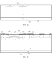
- FIG. 3a is a cross-sectional schematic view of the device after the P type buried layer 203 is formed.
- the second epitaxial layer is formed on the surface of the first epitaxial layer after the P-type buried layer 203 is formed.
- the P type buried layer 203 is at least in contact with the one first well 205.
- ions of the second conduction type are implanted and a first well is formed in the first conduction type region by driving-in.
- the P-type ions are implanted into the N type region and the first well 205 is formed in the N type region by driving-in.
- a field oxide layer and a gate oxide layer are grown, and a polysilicon layer is formed.
- a thick field oxide layer is grown on the surface of the N type region and then the gate oxide layer is grown, and the polysilicon layer 604 is formed on the surface of the N type region.
- ions of the second conduction type are implanted into the first conduction type region and a plurality of second wells are formed by driving-in.
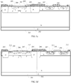
- FIG. 3b is a cross-sectional schematic view of the device after the step S550 is completed.
- a step of implanting ions of the P type into the second well 207 is further included, to form the UIS region 208 in the second wells 207 of the JFET region and the power device region.
- a step of forming the implanting barrier layer is further included prior to the step of implanting ions of the P type to form the UIS region 208.
- the implanting barrier layer is formed by re-forming one oxide layer.
- the oxide layer at the implanting window for implanting ions of the P type to form the UIS region 208 is thin, the implanted ions of the P type by high-energy can pass through the oxide layer to form the UIS region 208.
- the oxide layer at other positions is formed on the structures such as the field oxide layer and the polysilicon layer 604, so that the thickness of the entire implanting barrier layer is thick, and the ions of the P type are difficult to pass through the implanting barrier layer and to enter the N type region.
- ions of the first conduction type are implanted, to form a JFET source at the JFET region, and form a power device source at the power device region.
- the ions of the N type ion are implanted with the photoresist as a mask by using a photoetching process.
- the JFET source is formed in the second well 207 of the JFET region, and a VDMOS source 209 is formed in the second well 207 of the power device region.
- the VDMOS source 209 is formed in each second well 207 on both sides of the gate, and is divided into two blocks in each second well 207, leaving a position for the ohmic contact region 210 formed in the subsequent step in the middle.
- a step of forming the gate ohmic contact 214 and the ohmic contact region 210 in the first well 205 and the second well 207 is further included.
- the JFET gate ohmic contact 214 is formed in the first well 205 and the second well 207 of the JFET region
- the ohmic contact region 210 is formed in the second well 207 of the power device region.
- a contact hole is photoetched and etched, the metal layer is deposited, and the metal layer is filled into the contact hole, to form a metal electrode of the JFET source, a JFET metal gate and a metal contact of the power device source respectively.
- the metal filled into the contact hole is in contact with the JFET gate ohmic contact 214 to form the JFET metal gate 213, and is in contact with the JFET source 212 to form the metal electrode of the JFET source.
- a passivation layer is formed on the surface of the device, and the cross-section of the completed device is shown in FIG. 1 .
- the above mentioned device integrated with JFET improves the stability of the pinch-off voltage, solidifies the breakdown point, strengthens the UIS capability, is completely matched with the process, and realizes adjustability of the pinch-off voltage on the basis of the conventional technology.
- the step S520 includes: forming one first well 205 at a boundary between the JFET region and the power device region as an isolation well, and the isolation well is configured to isolate the JFET region from the power device region.
- an implantation concentration of the first well 205 of the step S530 is between 1.5E13 cm -2 and 2.2E13 cm -2 , and the well depth of the first well 205 is between 8.5 microns and 13.5 microns.
Landscapes
- Junction Field-Effect Transistors (AREA)
- Metal-Oxide And Bipolar Metal-Oxide Semiconductor Integrated Circuits (AREA)
- Engineering & Computer Science (AREA)
- Manufacturing & Machinery (AREA)
- Chemical & Material Sciences (AREA)
- Chemical Kinetics & Catalysis (AREA)
- General Chemical & Material Sciences (AREA)
- Insulated Gate Type Field-Effect Transistor (AREA)
Abstract
Description
- The present disclosure relates to semiconductor manufacturing technology, and more particularly to a device integrated with a junction field effect transistor (JFET). In addition, the present disclosure also relates to a method for manufacturing a device integrated with JFET.
- Integrating a high-voltage junction field effect transistor (JFET) on high-voltage process platform is an advanced development and concept in the recent field of smart power integrated circuit, which can greatly improve the on-state performance of vertical power devices, and significantly reduce the chip area, thereby meeting the mainstream trend for manufacturing the smart power device nowadays.
- The conventional structure of high-voltage integrated JFET can be achieved by a simpler process, but it cannot be applied in the smart power integrated field on a large scale due to the unstable pinch-off voltage thereof.
- As to a conventional Vertical Double-diffused MOSFET (VDMOS) integrated JFET, the current flows through the JFET from the bottom drain terminal and flows out of source 2 when the VDMOS is in turn-on stage. When a gradually increased voltage Vg2 is applied to the source 2, and in the same time, the same voltage Vg1 is applied to the gate; when the Vg2 > the pinch-off voltage Voff, the depletion layer of the JFET blocks the current, that is, a pinch-off phenomenon occurs. At this time, Vg1 > Vth (Vth is the threshold voltage of VDMOS), VDMOS is turned on, and a turn-on process is completed. Then the JFET absorbs an abrupt current of the VDMOS on the Miller platform, which makes the startup more gradual, and the current can be approximately linearly transformed. Therefore, the JFET has a significant effect for the stability of the device during the startup process. The power devices have an advantage of integrating parasitic JFET on process platforms thereof.
- The most important characteristics of the integrated parasitic JFET are the stability of the overall breakdown voltage and of the pinch-off voltage. The most ideal is that the breakdown voltage of the device remains the same after being integrated, and the breakdown point is preferably maintained at the breakdown point of the power VDMOS. The joint of the conventional integrated structure VDMOS and JFET only uses the substrate for isolation, and only the lateral distance of the substrate epitaxy can be extended to ensure the margin when depleted, which may increase the area of the entire die. Meanwhile, since the epitaxial layer specifications have deviation, the breakdown point may transfer if a slight change occurs in the process, and the breakdown point may transfer from the cell region of the body to the JFET region or the joint, which greatly reduces the stability of the breakdown and results in a phenomenon of breakdown voltage creep. The conventional structure generally uses a self-aligned P-type implanted substrate as a P-type pinch-off substrate. Since the P-type substrate of the cell region of the VDMOS has a very shallow depth of the longitudinal junction (generally onlyfrom 3 microns to 5 microns), the longitudinal channel of the JFET is very short, the length thereof cannot be adjusted, and then the pinch-off voltage is very unstable. It can be seen that the pinch-off voltage Voff may increase from 11 V up to 20 V when the drain voltage changes from 50 V to 100 V by simulation. However, it needs a stable Voff in practical applications, therefore the conventional structure is difficult to meet the actual requirement.
- According to various embodiments of the present disclosure, it is necessary to provide a device integrated with a junction field effect transistor (JFET) and method for manufacturing the same to solve the problem that the pinch-off voltage of the conventional JFET is unstable.
- A device integrated with JFET, the device is divided into a JFET region and a power device region, and the device includes: a drain with a first conduction type, while a part of the drain is located in the JFET region and the other part of the drain is located in the power device region; and a first conduction type region disposed on a front surface of the drain, while a part of the first conduction type region is located in the JFET region, and the other part of the first conduction type region is located in the power device region; the JFET region includes: a first well with a second conduction type, which is formed in the first conduction type region; a second well with a second conduction type, which is formed in the first conduction type region, while an ion concentration of the second well is higher than an ion concentration of the first well and the first conduction type is opposite to the second conduction type; a JFET source with the first conduction type; a metal electrode formed on the JFET source, which is in contact with the JFET source; and a second conduction type buried layer formed under the JFET source and the second well. A method for manufacturing a device integrated with JFET, the device includes a JFET region and a power device region, and the method includes: providing a substrate of a first conduction type, and a first conduction type region is formed on the substrate; while the first conduction type is opposite to the second conduction type; forming a second conduction type buried layer in the first conduction type region of the JFET region; implanting ions of the second conduction type into the first conduction type region, and forming a first well in the first conduction type region by driving-in; growing a field oxide layer and a gate oxide layer in turn, and forming a polysilicon layer on the surface of the first conduction type region; implanting the ions of the second conduction type into the first conduction type region and forming a plurality of second wells by driving-in; implanting ions of the first conduction type, to form a JFET source at the JFET region and form a power device source at the power device region; and photoetching and etching a contact hole, depositing a metal layer, filling the metal layer into the contact hole, to form a metal electrode of the JFET source, a JFET metal gate and a metal contact of the power device source respectively.
- The details of one or more embodiments of the present disclosure are set forth in the accompanying drawings and description below. Other features, objects, and advantages of the present disclosure will be apparent from the description, drawings and claims.
- To illustrate the technical solutions according to the embodiments of the present disclosure or in the prior art more clearly, the accompanying drawings for describing the embodiments or the prior art are introduced briefly in the following. Apparently, the accompanying drawings in the following description are only some embodiments of the present disclosure, and persons of ordinary skill in the art can derive other drawings from the accompanying drawings without creative efforts.
-
FIG. 1 is a schematic view of a cross-sectional structure of a device integrated with JFET in an embodiment; -
FIG. 2 is a flowchart of a method for manufacturing a device integrated with JFET in an embodiment; and -
FIG. 3a to FIG. 3d are cross-sectional schematic views of the manufacturing method described inFIG. 2 in the process of manufacturing the device. - For the convenience of understanding the present disclosure, a more comprehensive description of the present disclosure will be made according to the relevant drawings below. One or more preferred embodiments of the disclosure are given in drawings. However, the present disclosure may be implemented in many different forms and is not limited to the embodiments described herein. On the contrary, the purpose of providing these embodiments is to make the disclosure of the disclosure more thorough and comprehensive.
- Unless otherwise defined, all terms (including technical and scientific terms) used herein have the same meaning as commonly understood by one of ordinary skill in the art to which this disclosure belongs. The terms used in the specification of the present application are only for the purpose of describing specific embodiments, and not to limit the present application. The term "and/or" used herein includes any and all combinations of one or more relevant listed items.
- It should be understood that when an element is referred to as being "disposed" or "provided" on another element, it can be directly on the other element or intervening elements may be present. When an element is referred to as being "connected" or "coupled" to another element, it can be directly connected or coupled to another element or intervening elements may be present. The terms "vertical", "horizontal", "up", "down", "left", "right", and the like, as used herein are for illustrative purposes only.
- The semiconductor field of terms used herein are common technical terms used by those persons skilled in the art, for example, as to a P type impurity and an N type impurity, in order to distinguish doping concentration, the P+ type is simply represented as the P type with heavy doping concentration, the P type is represented as the P type with normal doping concentration, and the P- type is represented as the P type with mild doping concentration, the N+ type is simply represented as the N type with heavy doping concentration, the N type is represented as the N type with normal doping concentration, and the N- type is represented as the N type with mild doping concentration.
-
FIG. 1 is a schematic view of cross-sectional structure of the device integrated with JFET in an embodiment. In the embodiment, the N type is defined as a first conduction type, the P type is defined as a second conduction type, and the device is VDMOS. As shown inFIG. 1 , the device is divided into a JFET region and a VDMOS region according to the structure thereof, thedrain 201 of the N type on the back surface of the device (that is, a surface facing downward inFIG. 1 ) is partly used for forming the JFET region, and is partly used for forming the VDMOS region. Similarly, the N type region (including a firstN type region 202 and a second N type region 204) on the front surface of drain 201 (that is, a surface facing upward inFIG. 1 ) is partly used for forming the JFET region, and is partly used for forming the VDMOS region. In the present embodiment, thedrain 201 is an N+ drain and the N type region is an N- epitaxial layer. In order to facilitate to form the P type buriedlayer 203, the N type region forms the firstN type region 202 and the secondN type region 204 respectively by twice epitaxial processes, it should be understood that in other embodiments, the N type region may also be a single-layer structure provided that the required P type buriedlayer 203 is formed. The variation of a thickness and concentration of the epitaxial layer may change the pinch-off voltage; the concentration is smaller, the epitaxial thickness is thinner (considering the backward expansion as well as the depth of P well, the total epitaxial thickness of the firstN type region 202 and the secondN type region 204 is generally greater than 4 microns (µm), and the thickness is typically between 4 microns and 7 microns), and the pinch-off effect is better. - In the present embodiment, the JEFT region includes:
- A
first well 205, which is a P- well and is formed in the N type region; - A
second well 207, which is a high-voltage P well and is formed in the N type region, and an ion concentration of thesecond well 207 is higher than an ion concentration of thefirst well 205. The second well 207 forms a conduction channel as an N type contact of the device; - A
JFET source 212, theN+ JFET source 212 serves as the source contact of the JFET; - A metal electrode of the JFET source, which is formed on the
JFET source 212, which is in contact with theJFET source 212; - The P type buried
layer 203, which is formed under theJFET source 212 and thesecond well 207. - The above mentioned device integrated with JFET applies the lateral channel formed by the P type buried
layer 203 and thesecond well 207, so that the channel concentration is more uniform, and a longer lateral channel is designed by layout, and the pinch-off voltage thereof may be more stable. - The embodiment as shown in
FIG. 1 , a boundary between the JEFT region and the VDMOS region also forms one first well 205, as an isolation well configured to isolate the JEFT region from the VDMOS region. The P-first well 205 is used to assist depletion isolation. The flow-through path of the current can be completely blocked by the deeper P- well isolation, which prevents electric leakage between JFET and VDMOS. In addition, the lower N- epitaxial layer (that is, the first N type region 202) can be assisted to participate in depletion when the device is biased reversely and can withstand the voltage, and the breakdown voltage of the local area can be increased to serve for solidifying the breakdown point. At the same time, thefirst well 205 serves as the depletion structure of the terminal in the junction terminal extension technology, and can effectively shorten the chip area of the high-voltage VDMOS. In addition, since the junction process of the junction terminal extension exists, the junction depth of the first well 205 greatly exceeds the junction depth of the P type substrate of the VDMOS in the conventional art, thereby resulting in a longer longitudinal current channel. Compared with the conventional structure, the stability of the pinch-off voltage of the device is significantly improved, and the pinch-off voltage is also significantly reduced. - The embodiment as shown in
FIG. 1 , The JFET region further includes aJFET metal gate 213 and a JFET gateohmic contact 214. TheJFET metal gate 213 is formed on the JFET gateohmic contact 214 and is in contact with the JFET gateohmic contact 214. Each of the JFET gateohmic contacts 214 is formed in thefirst well 205 and the second well 207 of the JFET region respectively, and the each of JFET gateohmic contacts 214 is equipotentially connected with each other via theJFET metal gate 213. - In one embodiment, the P type buried
layer 203 is at least in contact with onefirst well 205. In the embodiment as shown inFIG. 1 , there is one P type buriedlayer 203 on each of two sides under thesecond well 207, and the two P type buriedlayers 203 are in contact with the one first well 205 respectively. The first well 205 formed by the deep well diffusion is connected to the P type buriedlayer 203, and the potential of the P type buriedlayer 203 can be led out, thereby preventing the P-type buriedlayer 203 from floating, so that the pinch-off voltage thereof can be more stable as the drain voltage changes. - In the embodiment as shown in
FIG. 1 , theJFET source 212 is formed between thesecond well 207 and the first well 205 (onefirst well 205 is adjacent to the second well 207). - In the embodiment as shown in
FIG. 1 , the VDMOS region includes agate 206, asecond well 207, anN+ VDMOS source 209 disposed in thesecond well 207, and an Unclamped Inductive Switching (UIS)region 208 of the P++ type disposed under theVDMOS source 209. The ion concentration of theUIS region 208 is higher than the ion concentration of thesecond well 207. In the embodiment as shown inFIG. 1 , The JFET region is also formed with theUIS region 208. Specifically, theUIS region 208 is disposed under the JFET gateohmic contact 214 in thesecond well 207, and in the present embodiment, is in thesecond well 207. In the other embodiments, theUIS region 208 may also be outside thesecond well 207 and be in thefirst well 205. TheUIS region 208 can reduce the base resistance of the parasitic NPN transistor and increase the avalanche tolerance of the device. - In the embodiment as shown in
FIG. 1 , there is one second well 207 formed on each of the two sides under thegate 206. TheVDMOS source 209 is formed in the twosecond wells 207, and theVDMOS source 209 is divided into two blocks in each of the twosecond wells 207. The device further includes a P+ typeohmic contact region 210 formed between the two blocks of theVDMOS source 209. -
FIG. 2 is a flowchart of a method for manufacturing a device integrated with JFET in an embodiment. The following method for manufacturing the device integrated with JFET will be introduced, in which the device is VDMOS, the first conduction type is an N type, and the second conduction type is a P type. - At step S510, a substrate of the first conduction type is provided, and a first conduction type region is formed on the substrate.
- In the present embodiment, an N type region is formed on the N+ substrate by epitaxy, and the substrate will serve as the
drain 201 of the device subsequently. - At step S520, a second conduction type buried layer is formed in the first conduction type region of the JFET region.
- In the present embodiment, the first conduction type region includes a first epitaxial layer (that is, the first N type layer 202) and a second epitaxial layer (that is, the second N type layer 204). The Step S520 is to photoetch the first epitaxial layer, implant P type ions, and form the P type buried
layer 203 by driving-in.FIG. 3a is a cross-sectional schematic view of the device after the P type buriedlayer 203 is formed. The second epitaxial layer is formed on the surface of the first epitaxial layer after the P-type buriedlayer 203 is formed. The P type buriedlayer 203 is at least in contact with the onefirst well 205. - At step S530, ions of the second conduction type are implanted and a first well is formed in the first conduction type region by driving-in.
- In the present embodiment, The P-type ions are implanted into the N type region and the
first well 205 is formed in the N type region by driving-in. - At step S540, a field oxide layer and a gate oxide layer are grown, and a polysilicon layer is formed.
- A thick field oxide layer is grown on the surface of the N type region and then the gate oxide layer is grown, and the
polysilicon layer 604 is formed on the surface of the N type region. - At step S550, ions of the second conduction type are implanted into the first conduction type region and a plurality of second wells are formed by driving-in.
- In the present embodiment, ions of the P type are implanted into the N type region by serving the field oxide layer and the
polysilicon layer 604 as a mask, and the plurality of thesecond wells 207 are formed by driving-in.FIG. 3b is a cross-sectional schematic view of the device after the step S550 is completed. - Referring to
FIG. 3c , in the present embodiment, prior to performing a step S560, a step of implanting ions of the P type into thesecond well 207 is further included, to form theUIS region 208 in thesecond wells 207 of the JFET region and the power device region. In order to prevent adversely affecting the channel region by implanting ions of the P type into thesecond well 207, in the present embodiment, a step of forming the implanting barrier layer is further included prior to the step of implanting ions of the P type to form theUIS region 208. In the present embodiment, the implanting barrier layer is formed by re-forming one oxide layer. Since the oxide layer at the implanting window for implanting ions of the P type to form theUIS region 208 is thin, the implanted ions of the P type by high-energy can pass through the oxide layer to form theUIS region 208. The oxide layer at other positions is formed on the structures such as the field oxide layer and thepolysilicon layer 604, so that the thickness of the entire implanting barrier layer is thick, and the ions of the P type are difficult to pass through the implanting barrier layer and to enter the N type region. - At step S560, ions of the first conduction type are implanted, to form a JFET source at the JFET region, and form a power device source at the power device region.
- Referring
FIG. 3d , in the present embodiment, the ions of the N type ion are implanted with the photoresist as a mask by using a photoetching process. The JFET source is formed in the second well 207 of the JFET region, and aVDMOS source 209 is formed in the second well 207 of the power device region. TheVDMOS source 209 is formed in each second well 207 on both sides of the gate, and is divided into two blocks in each second well 207, leaving a position for theohmic contact region 210 formed in the subsequent step in the middle. - In the present embodiment, after the step S560 is completed, a step of forming the gate
ohmic contact 214 and theohmic contact region 210 in thefirst well 205 and thesecond well 207 is further included. Specifically, the JFET gateohmic contact 214 is formed in thefirst well 205 and the second well 207 of the JFET region, and theohmic contact region 210 is formed in the second well 207 of the power device region. - At step S570, a contact hole is photoetched and etched, the metal layer is deposited, and the metal layer is filled into the contact hole, to form a metal electrode of the JFET source, a JFET metal gate and a metal contact of the power device source respectively.
- The metal filled into the contact hole is in contact with the JFET gate
ohmic contact 214 to form theJFET metal gate 213, and is in contact with theJFET source 212 to form the metal electrode of the JFET source. After depositing the metal layer, a passivation layer is formed on the surface of the device, and the cross-section of the completed device is shown inFIG. 1 . - Combining with the above mentioned advantages, the above mentioned device integrated with JFET improves the stability of the pinch-off voltage, solidifies the breakdown point, strengthens the UIS capability, is completely matched with the process, and realizes adjustability of the pinch-off voltage on the basis of the conventional technology.
- In one of the embodiments, the step S520 includes: forming one first well 205 at a boundary between the JFET region and the power device region as an isolation well, and the isolation well is configured to isolate the JFET region from the power device region.
- In one embodiment, an implantation concentration of the first well 205 of the step S530 is between 1.5E13 cm-2 and 2.2E13 cm-2, and the well depth of the
first well 205 is between 8.5 microns and 13.5 microns. - The above described embodiments are merely illustrative of several embodiments of the present disclosure, and the description thereof is more specific and detailed, but is not to be construed as limiting the scope of the present disclosure. It should be noted that several variations and modifications may be made by those persons skilled in the art and belong to the scope of protection of the present disclosure without departing from the spirit. Therefore, the scope of protection of the present disclosure should be subject to the appended claims.
Claims (18)
- A device integrated with a junction field effect transistor (JFET), the device is divided into a JFET region and a power device region, and the device comprises:a drain with a first conduction type, while a part of the drain is located in the JFET region and the other part of the drain is located in the power device region; anda first conduction type region disposed on a front surface of the drain, while a part of the first conduction type region is located in the JFET region, and the other part of the first conduction type region is located in the power device region;the JFET region comprises:a first well with a second conduction type, which is formed in the first conduction type region;a second well with a second conduction type, which is formed in the first conduction type region, while an ion concentration of the second well is higher than an ion concentration of the first well and the first conduction type is opposite to the second conduction type;a JFET source with the first conduction type;a metal electrode formed on the JFET source, which is in contact with the JFET source; anda second conduction type buried layer formed under the JFET source and the second well.
- The device of claim 1, wherein further comprising:
an isolation well located at a boundary between the JEFT region and the power device region, to isolate the JEFT region from the power device region. - The device of claim 2, wherein the JFET region further comprises a JFET metal gate and a JFET gate ohmic contact, the JFET metal gate is formed on the JFET gate ohmic contact and in contact with the JFET gate ohmic contact, the JFET gate ohmic contact is formed in the first well and the second well of the JFET region and the isolation well, and each of the JFET gate ohmic contacts is equipotentially connected with each other via the JFET metal gate.
- The device of claim 3, wherein the second conduction type buried layer is at least in contact with the first well of the JFET region.
- The device of claim 1, wherein the JFET source is formed between the second well of the JFET region and the first well of the JFET region being adjacent to the second well of the JFET region.
- The device of claim 1, wherein the device is a vertical double-diffused metal-oxide-semiconductor field-effect transistor (VDMOS).
- The device of claim 6, wherein the power device region comprises:a gate;a second well;a VDMOS source disposed in the second well of the power device region and having the first conduction type; andan unclamped inductive switching region disposed in the second well of the power device region and under the VDMOS source, while the unclamped inductive switching region has the second conduction type, and an ion concentration of the unclamped inductive switching region is higher than an ion concentration of the second well of the power device region.
- The device integrated with the junction field effect transistor of claim 7, wherein one second well of the power device region exists on each of two sides under the gate, the VDMOS source is formed in the two second wells of the power device region, and the VDMOS source is divided into two blocks in each of the two second wells of the power device region, and the device further comprises an ohmic contact region of the second conduction type formed between the two blocks of the VDMOS source.
- The device of claim 1, wherein the first conduction type is an N type, the second conduction type is a P type, and the first conduction type region is an N type epitaxial layer.
- The device of claim 9, wherein the N type epitaxial layer comprises a first N type region and a second N type region on the first N type region.
- The device of claim 10, wherein a thickness of the N type epitaxial layer is between 4 microns and 7 microns.
- A method for manufacturing a device integrated with a junction field effect transistor (JFET), the device comprises a JFET region and a power device region, and the method comprises:providing a substrate of a first conduction type, wherein a first conduction type region is formed on the substrate;forming a second conduction type buried layer in the first conduction type region of the JFET region; while the first conduction type is opposite to the second conduction type;implanting ions of the second conduction type into the first conduction type region and forming a first well of the JFET region in the first conduction type region by driving-in;growing a field oxide layer and a gate oxide layer on a surface of the first conduction type region in turn, and forming a polysilicon layer on the surface of the first conduction type region;implanting the ions of the second conduction type into the first conduction type region and forming a plurality of second wells of the JFET region by driving-in;implanting ions of the first conduction type, to form a JFET source at the JFET region and form a power device source at the power device region; andphotoetching and etching a contact hole, depositing a metal layer, filling the metal layer into the contact hole, to form a metal electrode of the JFET source, a JFET metal gate and a metal contact of the power device source respectively.
- The method of claim 12, wherein the step of forming an isolation well in the first conduction type region comprises: forming the isolation well at a boundary between the JFET region and the power device region, as isolation of the JFET region and the power device region.
- The method of claim 12, wherein the first conduction type region comprises a first epitaxial layer and a second epitaxial layer; the step of forming the second conduction type buried layer in the first conduction type region of the JFET region comprises:
photoetching the first epitaxial layer, implanting the ions of the second conduction type, and forming the second conduction type buried layer by driving-in; prior to the step of implanting the ions of the second conduction type into the first conduction type region and forming the first well in the first conduction type region by driving-in, further comprising a step of forming the second epitaxial layer on a surface of the first epitaxial layer; the second conduction type buried layer is at least in contact with the first well of the JFET region. - The method of claim 12, wherein after the step of implanting the ions of the second conduction type into the first conduction type region and forming the plurality of the second wells of the JFET region by driving-in, and prior to the step of implanting the ions of the first conduction type, further comprising a step of forming an implanting barrier layer, and a step of implanting the ions of the second conduction type into the second well of the JFET region to form an unclamped inductive switching region, and the implanting energy of the unclamped inductive switching region is greater than the implanting energy of the step of implanting the ions of the first conduction type.
- The method of claim 12, wherein after the step of forming the JFET source at the JFET region and forming the power device source at the power device region, and prior to the step of photoetching and etching the contact hole, further comprising a step of implanting the ions of the second conduction type, to form JFET gate ohmic contacts in the first well and the second well of the JFET region, and form an ohmic contact region in the second well of the power device region.
- The method of claim 12, wherein the first conduction type is an N type, the second conduction type is a P type, and the device is a vertical double-diffused metal-oxide-semiconductor field-effect transistor (VDMOS).
- The method of claim 12, wherein in the step of implanting the ions of the second conduction type into the first conduction type region and driving-in, an implanting concentration is between 1.5E13 cm-2 and 2.2E13 cm-2; and
in the step of forming the first well in the first conduction type region, a well depth of the formed first well is between 8.5 microns and 13.5 microns.
Applications Claiming Priority (2)
| Application Number | Priority Date | Filing Date | Title |
|---|---|---|---|
| CN201610794437.6A CN107785411B (en) | 2016-08-31 | 2016-08-31 | Device integrated with junction field effect transistor and manufacturing method thereof |
| PCT/CN2017/099841 WO2018041192A1 (en) | 2016-08-31 | 2017-08-31 | Component having integrated junction field-effect transistor, and method for manufacturing same |
Publications (3)
| Publication Number | Publication Date |
|---|---|
| EP3509110A1 true EP3509110A1 (en) | 2019-07-10 |
| EP3509110A4 EP3509110A4 (en) | 2020-03-11 |
| EP3509110B1 EP3509110B1 (en) | 2025-03-05 |
Family
ID=61300063
Family Applications (1)
| Application Number | Title | Priority Date | Filing Date |
|---|---|---|---|
| EP17845494.8A Active EP3509110B1 (en) | 2016-08-31 | 2017-08-31 | Component having integrated junction field-effect transistor, and method for manufacturing same |
Country Status (5)
| Country | Link |
|---|---|
| US (1) | US10872823B2 (en) |
| EP (1) | EP3509110B1 (en) |
| JP (1) | JP6986553B2 (en) |
| CN (1) | CN107785411B (en) |
| WO (1) | WO2018041192A1 (en) |
Families Citing this family (6)
| Publication number | Priority date | Publication date | Assignee | Title |
|---|---|---|---|---|
| JP7329348B2 (en) * | 2019-03-27 | 2023-08-18 | ローム株式会社 | semiconductor equipment |
| DE102020004758A1 (en) * | 2019-08-30 | 2021-03-04 | Semiconductor Components Industries, Llc | SILICON CARBIDE FIELD EFFECT TRANSISTORS |
| US11139394B2 (en) * | 2019-08-30 | 2021-10-05 | Semiconductor Components Industries, Llc | Silicon carbide field-effect transistors |
| CN111900197B (en) * | 2020-07-29 | 2023-06-23 | 杰华特微电子股份有限公司 | Junction field effect transistor, manufacturing method thereof, and semiconductor chip |
| CN116314338B (en) * | 2023-05-18 | 2023-08-01 | 深圳平创半导体有限公司 | Semiconductor structure and preparation method thereof |
| CN119894081A (en) * | 2025-01-21 | 2025-04-25 | 华虹半导体(无锡)有限公司 | Semiconductor structure and forming method thereof |
Family Cites Families (14)
| Publication number | Priority date | Publication date | Assignee | Title |
|---|---|---|---|---|
| US4454523A (en) * | 1981-03-30 | 1984-06-12 | Siliconix Incorporated | High voltage field effect transistor |
| JP2949745B2 (en) * | 1990-01-19 | 1999-09-20 | 日本電気株式会社 | Method of manufacturing vertical MOS field effect transistor |
| JPH10107214A (en) * | 1996-10-01 | 1998-04-24 | Masashi Mukogawa | Semiconductor device |
| JP3666280B2 (en) * | 1999-01-20 | 2005-06-29 | 富士電機ホールディングス株式会社 | Silicon carbide vertical FET and method of manufacturing the same |
| EP1058303A1 (en) | 1999-05-31 | 2000-12-06 | STMicroelectronics S.r.l. | Fabrication of VDMOS structure with reduced parasitic effects |
| CN1866542B (en) | 2005-05-18 | 2010-04-28 | 崇贸科技股份有限公司 | MOS field effect transistor with isolation structure and manufacturing method thereof |
| CN2836242Y (en) | 2005-10-14 | 2006-11-08 | 西安电子科技大学 | Integrated high-voltage VDMOS transistor structure |
| JP5321377B2 (en) * | 2009-09-11 | 2013-10-23 | 三菱電機株式会社 | Power semiconductor device |
| US8354698B2 (en) | 2010-01-28 | 2013-01-15 | System General Corp. | VDMOS and JFET integrated semiconductor device |
| JP5997426B2 (en) * | 2011-08-19 | 2016-09-28 | 株式会社日立製作所 | Semiconductor device and manufacturing method of semiconductor device |
| US8963218B2 (en) * | 2011-09-30 | 2015-02-24 | Maxim Integrated Products, Inc. | Dual-gate VDMOS device |
| CN102339755A (en) * | 2011-09-30 | 2012-02-01 | 上海先进半导体制造股份有限公司 | High-voltage N-type junction field effect transistor and manufacturing method thereof |
| CN102916049B (en) | 2012-10-30 | 2015-04-22 | 成都芯源系统有限公司 | Semiconductor device including junction field effect transistor and method of manufacturing the same |
| US9460926B2 (en) * | 2014-06-30 | 2016-10-04 | Alpha And Omega Semiconductor Incorporated | Forming JFET and LDMOS transistor in monolithic power integrated circuit using deep diffusion regions |
-
2016
- 2016-08-31 CN CN201610794437.6A patent/CN107785411B/en active Active
-
2017
- 2017-08-31 WO PCT/CN2017/099841 patent/WO2018041192A1/en not_active Ceased
- 2017-08-31 US US16/329,550 patent/US10872823B2/en active Active
- 2017-08-31 EP EP17845494.8A patent/EP3509110B1/en active Active
- 2017-08-31 JP JP2019511843A patent/JP6986553B2/en active Active
Also Published As
| Publication number | Publication date |
|---|---|
| EP3509110A4 (en) | 2020-03-11 |
| CN107785411A (en) | 2018-03-09 |
| JP6986553B2 (en) | 2021-12-22 |
| US10872823B2 (en) | 2020-12-22 |
| WO2018041192A1 (en) | 2018-03-08 |
| EP3509110B1 (en) | 2025-03-05 |
| US20190259669A1 (en) | 2019-08-22 |
| JP2019532499A (en) | 2019-11-07 |
| CN107785411B (en) | 2020-06-12 |
Similar Documents
| Publication | Publication Date | Title |
|---|---|---|
| US10720511B2 (en) | Trench transistors and methods with low-voltage-drop shunt to body diode | |
| US10453955B2 (en) | Lateral DMOS device with dummy gate | |
| EP3509110B1 (en) | Component having integrated junction field-effect transistor, and method for manufacturing same | |
| KR100904378B1 (en) | Power Morse Device | |
| US10861965B2 (en) | Power MOSFET with an integrated pseudo-Schottky diode in source contact trench | |
| EP3509101B1 (en) | Device integrating a junction field effect transistor and manufacturing method therefor | |
| US8841718B2 (en) | Pseudo self aligned radhard MOSFET and process of manufacture | |
| EP3509102B1 (en) | Component integrated with depletion-mode junction field-effect transistor and method for manufacturing component | |
| WO2017211105A1 (en) | Super-junction device, chip and manufacturing method therefor | |
| WO2018041082A1 (en) | Device integrating junction field-effect transistor and manufacturing method therefor | |
| CN111223931A (en) | Trench MOSFET and method of making the same | |
| CN105914233B (en) | A kind of high robust restores superjunction power semiconductor transistor and preparation method thereof soon | |
| TWI385802B (en) | High-voltage metal-oxide semiconductor device and fabrication method thereof | |
| CN101728430A (en) | High voltage metal oxide semiconductor assembly and manufacturing method thereof |
Legal Events
| Date | Code | Title | Description |
|---|---|---|---|
| STAA | Information on the status of an ep patent application or granted ep patent |
Free format text: STATUS: THE INTERNATIONAL PUBLICATION HAS BEEN MADE |
|
| PUAI | Public reference made under article 153(3) epc to a published international application that has entered the european phase |
Free format text: ORIGINAL CODE: 0009012 |
|
| STAA | Information on the status of an ep patent application or granted ep patent |
Free format text: STATUS: REQUEST FOR EXAMINATION WAS MADE |
|
| 17P | Request for examination filed |
Effective date: 20190327 |
|
| AK | Designated contracting states |
Kind code of ref document: A1 Designated state(s): AL AT BE BG CH CY CZ DE DK EE ES FI FR GB GR HR HU IE IS IT LI LT LU LV MC MK MT NL NO PL PT RO RS SE SI SK SM TR |
|
| AX | Request for extension of the european patent |
Extension state: BA ME |
|
| DAV | Request for validation of the european patent (deleted) | ||
| DAX | Request for extension of the european patent (deleted) | ||
| A4 | Supplementary search report drawn up and despatched |
Effective date: 20200211 |
|
| RIC1 | Information provided on ipc code assigned before grant |
Ipc: H01L 29/66 20060101ALN20200205BHEP Ipc: H01L 29/10 20060101ALI20200205BHEP Ipc: H01L 21/8232 20060101ALI20200205BHEP Ipc: H01L 29/808 20060101ALI20200205BHEP Ipc: H01L 29/78 20060101AFI20200205BHEP Ipc: H01L 27/085 20060101ALI20200205BHEP |
|
| STAA | Information on the status of an ep patent application or granted ep patent |
Free format text: STATUS: EXAMINATION IS IN PROGRESS |
|
| 17Q | First examination report despatched |
Effective date: 20210727 |
|
| GRAP | Despatch of communication of intention to grant a patent |
Free format text: ORIGINAL CODE: EPIDOSNIGR1 |
|
| STAA | Information on the status of an ep patent application or granted ep patent |
Free format text: STATUS: GRANT OF PATENT IS INTENDED |
|
| RIC1 | Information provided on ipc code assigned before grant |
Ipc: H01L 29/66 20060101ALN20240912BHEP Ipc: H01L 29/10 20060101ALI20240912BHEP Ipc: H01L 29/808 20060101ALI20240912BHEP Ipc: H01L 21/8232 20060101ALI20240912BHEP Ipc: H01L 27/085 20060101ALI20240912BHEP Ipc: H01L 29/78 20060101AFI20240912BHEP |
|
| INTG | Intention to grant announced |
Effective date: 20241004 |
|
| GRAS | Grant fee paid |
Free format text: ORIGINAL CODE: EPIDOSNIGR3 |
|
| GRAA | (expected) grant |
Free format text: ORIGINAL CODE: 0009210 |
|
| STAA | Information on the status of an ep patent application or granted ep patent |
Free format text: STATUS: THE PATENT HAS BEEN GRANTED |
|
| AK | Designated contracting states |
Kind code of ref document: B1 Designated state(s): AL AT BE BG CH CY CZ DE DK EE ES FI FR GB GR HR HU IE IS IT LI LT LU LV MC MK MT NL NO PL PT RO RS SE SI SK SM TR |
|
| REG | Reference to a national code |
Ref country code: GB Ref legal event code: FG4D |
|
| REG | Reference to a national code |
Ref country code: DE Ref legal event code: R096 Ref document number: 602017088200 Country of ref document: DE |
|
| REG | Reference to a national code |
Ref country code: IE Ref legal event code: FG4D |
|
| PG25 | Lapsed in a contracting state [announced via postgrant information from national office to epo] |
Ref country code: RS Free format text: LAPSE BECAUSE OF FAILURE TO SUBMIT A TRANSLATION OF THE DESCRIPTION OR TO PAY THE FEE WITHIN THE PRESCRIBED TIME-LIMIT Effective date: 20250605 |
|
| PG25 | Lapsed in a contracting state [announced via postgrant information from national office to epo] |
Ref country code: FI Free format text: LAPSE BECAUSE OF FAILURE TO SUBMIT A TRANSLATION OF THE DESCRIPTION OR TO PAY THE FEE WITHIN THE PRESCRIBED TIME-LIMIT Effective date: 20250305 |
|
| REG | Reference to a national code |
Ref country code: NL Ref legal event code: MP Effective date: 20250305 |
|
| PG25 | Lapsed in a contracting state [announced via postgrant information from national office to epo] |
Ref country code: ES Free format text: LAPSE BECAUSE OF FAILURE TO SUBMIT A TRANSLATION OF THE DESCRIPTION OR TO PAY THE FEE WITHIN THE PRESCRIBED TIME-LIMIT Effective date: 20250305 |
|
| REG | Reference to a national code |
Ref country code: LT Ref legal event code: MG9D |
|
| PG25 | Lapsed in a contracting state [announced via postgrant information from national office to epo] |
Ref country code: NO Free format text: LAPSE BECAUSE OF FAILURE TO SUBMIT A TRANSLATION OF THE DESCRIPTION OR TO PAY THE FEE WITHIN THE PRESCRIBED TIME-LIMIT Effective date: 20250605 |
|
| PG25 | Lapsed in a contracting state [announced via postgrant information from national office to epo] |
Ref country code: HR Free format text: LAPSE BECAUSE OF FAILURE TO SUBMIT A TRANSLATION OF THE DESCRIPTION OR TO PAY THE FEE WITHIN THE PRESCRIBED TIME-LIMIT Effective date: 20250305 |
|
| PG25 | Lapsed in a contracting state [announced via postgrant information from national office to epo] |
Ref country code: LV Free format text: LAPSE BECAUSE OF FAILURE TO SUBMIT A TRANSLATION OF THE DESCRIPTION OR TO PAY THE FEE WITHIN THE PRESCRIBED TIME-LIMIT Effective date: 20250305 |
|
| PG25 | Lapsed in a contracting state [announced via postgrant information from national office to epo] |
Ref country code: GR Free format text: LAPSE BECAUSE OF FAILURE TO SUBMIT A TRANSLATION OF THE DESCRIPTION OR TO PAY THE FEE WITHIN THE PRESCRIBED TIME-LIMIT Effective date: 20250606 Ref country code: BG Free format text: LAPSE BECAUSE OF FAILURE TO SUBMIT A TRANSLATION OF THE DESCRIPTION OR TO PAY THE FEE WITHIN THE PRESCRIBED TIME-LIMIT Effective date: 20250305 |
|
| REG | Reference to a national code |
Ref country code: AT Ref legal event code: MK05 Ref document number: 1773780 Country of ref document: AT Kind code of ref document: T Effective date: 20250305 |
|
| PG25 | Lapsed in a contracting state [announced via postgrant information from national office to epo] |
Ref country code: NL Free format text: LAPSE BECAUSE OF FAILURE TO SUBMIT A TRANSLATION OF THE DESCRIPTION OR TO PAY THE FEE WITHIN THE PRESCRIBED TIME-LIMIT Effective date: 20250305 |
|
| PG25 | Lapsed in a contracting state [announced via postgrant information from national office to epo] |
Ref country code: SE Free format text: LAPSE BECAUSE OF FAILURE TO SUBMIT A TRANSLATION OF THE DESCRIPTION OR TO PAY THE FEE WITHIN THE PRESCRIBED TIME-LIMIT Effective date: 20250305 |
|
| PG25 | Lapsed in a contracting state [announced via postgrant information from national office to epo] |
Ref country code: SM Free format text: LAPSE BECAUSE OF FAILURE TO SUBMIT A TRANSLATION OF THE DESCRIPTION OR TO PAY THE FEE WITHIN THE PRESCRIBED TIME-LIMIT Effective date: 20250305 |
|
| PG25 | Lapsed in a contracting state [announced via postgrant information from national office to epo] |
Ref country code: PT Free format text: LAPSE BECAUSE OF FAILURE TO SUBMIT A TRANSLATION OF THE DESCRIPTION OR TO PAY THE FEE WITHIN THE PRESCRIBED TIME-LIMIT Effective date: 20250707 |
|
| PGFP | Annual fee paid to national office [announced via postgrant information from national office to epo] |
Ref country code: DE Payment date: 20250820 Year of fee payment: 9 |
|
| PG25 | Lapsed in a contracting state [announced via postgrant information from national office to epo] |
Ref country code: IT Free format text: LAPSE BECAUSE OF FAILURE TO SUBMIT A TRANSLATION OF THE DESCRIPTION OR TO PAY THE FEE WITHIN THE PRESCRIBED TIME-LIMIT Effective date: 20250305 Ref country code: PL Free format text: LAPSE BECAUSE OF FAILURE TO SUBMIT A TRANSLATION OF THE DESCRIPTION OR TO PAY THE FEE WITHIN THE PRESCRIBED TIME-LIMIT Effective date: 20250305 |
|
| PGFP | Annual fee paid to national office [announced via postgrant information from national office to epo] |
Ref country code: GB Payment date: 20250821 Year of fee payment: 9 |
|
| PG25 | Lapsed in a contracting state [announced via postgrant information from national office to epo] |
Ref country code: AT Free format text: LAPSE BECAUSE OF FAILURE TO SUBMIT A TRANSLATION OF THE DESCRIPTION OR TO PAY THE FEE WITHIN THE PRESCRIBED TIME-LIMIT Effective date: 20250305 |
|
| PGFP | Annual fee paid to national office [announced via postgrant information from national office to epo] |
Ref country code: FR Payment date: 20250828 Year of fee payment: 9 |
|
| PG25 | Lapsed in a contracting state [announced via postgrant information from national office to epo] |
Ref country code: CZ Free format text: LAPSE BECAUSE OF FAILURE TO SUBMIT A TRANSLATION OF THE DESCRIPTION OR TO PAY THE FEE WITHIN THE PRESCRIBED TIME-LIMIT Effective date: 20250305 Ref country code: EE Free format text: LAPSE BECAUSE OF FAILURE TO SUBMIT A TRANSLATION OF THE DESCRIPTION OR TO PAY THE FEE WITHIN THE PRESCRIBED TIME-LIMIT Effective date: 20250305 |
|
| PG25 | Lapsed in a contracting state [announced via postgrant information from national office to epo] |
Ref country code: RO Free format text: LAPSE BECAUSE OF FAILURE TO SUBMIT A TRANSLATION OF THE DESCRIPTION OR TO PAY THE FEE WITHIN THE PRESCRIBED TIME-LIMIT Effective date: 20250305 |
|
| PG25 | Lapsed in a contracting state [announced via postgrant information from national office to epo] |
Ref country code: SK Free format text: LAPSE BECAUSE OF FAILURE TO SUBMIT A TRANSLATION OF THE DESCRIPTION OR TO PAY THE FEE WITHIN THE PRESCRIBED TIME-LIMIT Effective date: 20250305 |
|
| PG25 | Lapsed in a contracting state [announced via postgrant information from national office to epo] |
Ref country code: IS Free format text: LAPSE BECAUSE OF FAILURE TO SUBMIT A TRANSLATION OF THE DESCRIPTION OR TO PAY THE FEE WITHIN THE PRESCRIBED TIME-LIMIT Effective date: 20250705 |
|
| REG | Reference to a national code |
Ref country code: DE Ref legal event code: R097 Ref document number: 602017088200 Country of ref document: DE |
|
| PLBE | No opposition filed within time limit |
Free format text: ORIGINAL CODE: 0009261 |
|
| STAA | Information on the status of an ep patent application or granted ep patent |
Free format text: STATUS: NO OPPOSITION FILED WITHIN TIME LIMIT |
|
| PG25 | Lapsed in a contracting state [announced via postgrant information from national office to epo] |
Ref country code: DK Free format text: LAPSE BECAUSE OF FAILURE TO SUBMIT A TRANSLATION OF THE DESCRIPTION OR TO PAY THE FEE WITHIN THE PRESCRIBED TIME-LIMIT Effective date: 20250305 |
|
| REG | Reference to a national code |
Ref country code: CH Ref legal event code: L10 Free format text: ST27 STATUS EVENT CODE: U-0-0-L10-L00 (AS PROVIDED BY THE NATIONAL OFFICE) Effective date: 20260114 |
|
| 26N | No opposition filed |
Effective date: 20251208 |
|
| REG | Reference to a national code |
Ref country code: CH Ref legal event code: H13 Free format text: ST27 STATUS EVENT CODE: U-0-0-H10-H13 (AS PROVIDED BY THE NATIONAL OFFICE) Effective date: 20260324 |
|
| PG25 | Lapsed in a contracting state [announced via postgrant information from national office to epo] |
Ref country code: MC Free format text: LAPSE BECAUSE OF FAILURE TO SUBMIT A TRANSLATION OF THE DESCRIPTION OR TO PAY THE FEE WITHIN THE PRESCRIBED TIME-LIMIT Effective date: 20250305 |
|
| PG25 | Lapsed in a contracting state [announced via postgrant information from national office to epo] |
Ref country code: LU Free format text: LAPSE BECAUSE OF NON-PAYMENT OF DUE FEES Effective date: 20250831 |
|
| PG25 | Lapsed in a contracting state [announced via postgrant information from national office to epo] |
Ref country code: CH Free format text: LAPSE BECAUSE OF NON-PAYMENT OF DUE FEES Effective date: 20250831 |