EP3508898A1 - Light guide body, optical module, and method for adjusting optical axis of optical path - Google Patents
Light guide body, optical module, and method for adjusting optical axis of optical path Download PDFInfo
- Publication number
- EP3508898A1 EP3508898A1 EP17846117.4A EP17846117A EP3508898A1 EP 3508898 A1 EP3508898 A1 EP 3508898A1 EP 17846117 A EP17846117 A EP 17846117A EP 3508898 A1 EP3508898 A1 EP 3508898A1
- Authority
- EP
- European Patent Office
- Prior art keywords
- light guide
- guide body
- optical
- optical axis
- optical path
- Prior art date
- Legal status (The legal status is an assumption and is not a legal conclusion. Google has not performed a legal analysis and makes no representation as to the accuracy of the status listed.)
- Pending
Links
- 230000003287 optical effect Effects 0.000 title claims abstract description 134
- 238000000034 method Methods 0.000 title claims abstract description 18
- 239000013078 crystal Substances 0.000 claims abstract description 37
- 230000008033 biological extinction Effects 0.000 claims abstract description 34
- XUIMIQQOPSSXEZ-UHFFFAOYSA-N Silicon Chemical compound [Si] XUIMIQQOPSSXEZ-UHFFFAOYSA-N 0.000 claims abstract description 31
- 229910052710 silicon Inorganic materials 0.000 claims abstract description 31
- 239000010703 silicon Substances 0.000 claims abstract description 31
- 238000009434 installation Methods 0.000 claims abstract description 10
- 230000010287 polarization Effects 0.000 abstract description 23
- 230000002411 adverse Effects 0.000 abstract description 3
- 230000000052 comparative effect Effects 0.000 description 17
- 238000003780 insertion Methods 0.000 description 9
- 230000037431 insertion Effects 0.000 description 9
- VYPSYNLAJGMNEJ-UHFFFAOYSA-N silicon dioxide Inorganic materials O=[Si]=O VYPSYNLAJGMNEJ-UHFFFAOYSA-N 0.000 description 8
- 150000001875 compounds Chemical class 0.000 description 7
- 239000004065 semiconductor Substances 0.000 description 7
- 230000005540 biological transmission Effects 0.000 description 6
- 238000005259 measurement Methods 0.000 description 6
- 239000000853 adhesive Substances 0.000 description 4
- 230000001070 adhesive effect Effects 0.000 description 4
- 239000002223 garnet Substances 0.000 description 4
- 239000002923 metal particle Substances 0.000 description 3
- 239000010453 quartz Substances 0.000 description 3
- 239000004593 Epoxy Substances 0.000 description 2
- 230000015556 catabolic process Effects 0.000 description 2
- 229910052681 coesite Inorganic materials 0.000 description 2
- 229910052906 cristobalite Inorganic materials 0.000 description 2
- 238000006731 degradation reaction Methods 0.000 description 2
- 230000001419 dependent effect Effects 0.000 description 2
- 230000000694 effects Effects 0.000 description 2
- 238000004519 manufacturing process Methods 0.000 description 2
- 239000000463 material Substances 0.000 description 2
- 238000005498 polishing Methods 0.000 description 2
- 230000000644 propagated effect Effects 0.000 description 2
- 239000000377 silicon dioxide Substances 0.000 description 2
- 229910052682 stishovite Inorganic materials 0.000 description 2
- 229920001187 thermosetting polymer Polymers 0.000 description 2
- 229910052905 tridymite Inorganic materials 0.000 description 2
- 239000006117 anti-reflective coating Substances 0.000 description 1
- 230000003667 anti-reflective effect Effects 0.000 description 1
- 230000004323 axial length Effects 0.000 description 1
- 239000011248 coating agent Substances 0.000 description 1
- 238000000576 coating method Methods 0.000 description 1
- 238000004891 communication Methods 0.000 description 1
- 230000008878 coupling Effects 0.000 description 1
- 238000010168 coupling process Methods 0.000 description 1
- 238000005859 coupling reaction Methods 0.000 description 1
- 230000007423 decrease Effects 0.000 description 1
- 238000013461 design Methods 0.000 description 1
- 230000001771 impaired effect Effects 0.000 description 1
- 230000010354 integration Effects 0.000 description 1
- 238000000691 measurement method Methods 0.000 description 1
- 238000012545 processing Methods 0.000 description 1
- 229910001220 stainless steel Inorganic materials 0.000 description 1
- 239000010935 stainless steel Substances 0.000 description 1
Images

Classifications
-
- G—PHYSICS
- G02—OPTICS
- G02B—OPTICAL ELEMENTS, SYSTEMS OR APPARATUS
- G02B6/00—Light guides; Structural details of arrangements comprising light guides and other optical elements, e.g. couplings
- G02B6/24—Coupling light guides
- G02B6/42—Coupling light guides with opto-electronic elements
- G02B6/4201—Packages, e.g. shape, construction, internal or external details
- G02B6/4219—Mechanical fixtures for holding or positioning the elements relative to each other in the couplings; Alignment methods for the elements, e.g. measuring or observing methods especially used therefor
- G02B6/422—Active alignment, i.e. moving the elements in response to the detected degree of coupling or position of the elements
- G02B6/4227—Active alignment methods, e.g. procedures and algorithms
-
- G—PHYSICS
- G02—OPTICS
- G02B—OPTICAL ELEMENTS, SYSTEMS OR APPARATUS
- G02B6/00—Light guides; Structural details of arrangements comprising light guides and other optical elements, e.g. couplings
- G02B6/10—Light guides; Structural details of arrangements comprising light guides and other optical elements, e.g. couplings of the optical waveguide type
- G02B6/12—Light guides; Structural details of arrangements comprising light guides and other optical elements, e.g. couplings of the optical waveguide type of the integrated circuit kind
- G02B6/126—Light guides; Structural details of arrangements comprising light guides and other optical elements, e.g. couplings of the optical waveguide type of the integrated circuit kind using polarisation effects
-
- C—CHEMISTRY; METALLURGY
- C30—CRYSTAL GROWTH
- C30B—SINGLE-CRYSTAL GROWTH; UNIDIRECTIONAL SOLIDIFICATION OF EUTECTIC MATERIAL OR UNIDIRECTIONAL DEMIXING OF EUTECTOID MATERIAL; REFINING BY ZONE-MELTING OF MATERIAL; PRODUCTION OF A HOMOGENEOUS POLYCRYSTALLINE MATERIAL WITH DEFINED STRUCTURE; SINGLE CRYSTALS OR HOMOGENEOUS POLYCRYSTALLINE MATERIAL WITH DEFINED STRUCTURE; AFTER-TREATMENT OF SINGLE CRYSTALS OR A HOMOGENEOUS POLYCRYSTALLINE MATERIAL WITH DEFINED STRUCTURE; APPARATUS THEREFOR
- C30B29/00—Single crystals or homogeneous polycrystalline material with defined structure characterised by the material or by their shape
- C30B29/02—Elements
- C30B29/06—Silicon
-
- G—PHYSICS
- G02—OPTICS
- G02B—OPTICAL ELEMENTS, SYSTEMS OR APPARATUS
- G02B27/00—Optical systems or apparatus not provided for by any of the groups G02B1/00 - G02B26/00, G02B30/00
- G02B27/28—Optical systems or apparatus not provided for by any of the groups G02B1/00 - G02B26/00, G02B30/00 for polarising
-
- G—PHYSICS
- G02—OPTICS
- G02B—OPTICAL ELEMENTS, SYSTEMS OR APPARATUS
- G02B6/00—Light guides; Structural details of arrangements comprising light guides and other optical elements, e.g. couplings
- G02B6/24—Coupling light guides
- G02B6/42—Coupling light guides with opto-electronic elements
- G02B6/4201—Packages, e.g. shape, construction, internal or external details
- G02B6/4204—Packages, e.g. shape, construction, internal or external details the coupling comprising intermediate optical elements, e.g. lenses, holograms
- G02B6/4213—Packages, e.g. shape, construction, internal or external details the coupling comprising intermediate optical elements, e.g. lenses, holograms the intermediate optical elements being polarisation selective optical elements
-
- G—PHYSICS
- G02—OPTICS
- G02B—OPTICAL ELEMENTS, SYSTEMS OR APPARATUS
- G02B6/00—Light guides; Structural details of arrangements comprising light guides and other optical elements, e.g. couplings
- G02B6/24—Coupling light guides
- G02B6/26—Optical coupling means
- G02B6/27—Optical coupling means with polarisation selective and adjusting means
- G02B6/2706—Optical coupling means with polarisation selective and adjusting means as bulk elements, i.e. free space arrangements external to a light guide, e.g. polarising beam splitters
-
- G—PHYSICS
- G02—OPTICS
- G02B—OPTICAL ELEMENTS, SYSTEMS OR APPARATUS
- G02B6/00—Light guides; Structural details of arrangements comprising light guides and other optical elements, e.g. couplings
- G02B6/24—Coupling light guides
- G02B6/42—Coupling light guides with opto-electronic elements
- G02B6/4201—Packages, e.g. shape, construction, internal or external details
- G02B6/4219—Mechanical fixtures for holding or positioning the elements relative to each other in the couplings; Alignment methods for the elements, e.g. measuring or observing methods especially used therefor
- G02B6/422—Active alignment, i.e. moving the elements in response to the detected degree of coupling or position of the elements
-
- G—PHYSICS
- G02—OPTICS
- G02B—OPTICAL ELEMENTS, SYSTEMS OR APPARATUS
- G02B7/00—Mountings, adjusting means, or light-tight connections, for optical elements
- G02B7/003—Alignment of optical elements
Definitions
- the present invention relates to a light guide body, installed in an optical integrated module used in optical communication or optical measurement, and an optical module and an optical path and optical axis measurement method which use this.
- Compound semiconductor components a laser, a modulator, and the like
- waveguide circuit components made of Si a resonator, a multiplexer, a splitter, and the like
- the compound semiconductor components or Si waveguide circuit components have high polarization dependence, and their characteristics are dependent upon a polarization state of their incident light.
- Patent Literature 1 JP2004-347702A
- an object of the present invention to provide a light guide body which does not adversely affect the polarization characteristics and can easily perform the optical path and optical axis adjustment. Furthermore, another object is to provide an optical module and an optical path and optical axis adjustment method using such a light guide body.
- the present invention provides a light guide body for optical path and optical axis adjustment, the light guide body being characterized by including a silicon single crystal having an extinction ratio of 30 dB or more.
- the silicon single crystal Since the silicon single crystal has a high refractive index, an angle at which light is internally propagated and an exit position of the light greatly change, and a position of an optical axis can be easily greatly changed. Furthermore, when an extinction ratio of the silicon single crystal is 30 dB or more, a polarization plane of the light which is transmitted through the silicon single crystal is not considerably disordered. Thus, the light guide body according to the present invention can suppress a change in polarization characteristics and facilitate the optical path and optical axis adjustment.
- one side surface alone of the light guide body is joined and fixed to a base.
- the present invention provides an optical module including the light guide body installed at an installation angle adjusted for optical path and optical axis adjustment between components.
- optical path and optical axis adjustment is performed by the light guide body according to the present invention, polarization characteristics of light are hardly changed by the optical path and optical axis adjustment. Additionally, since the optical path and optical axis adjustment between components such as compound semiconductor components or Si waveguide circuit components can be carried out by a simple technique, the efficiency of designing and manufacturing the optical module can be improved.
- the present invention provides an optical path and optical axis adjustment method including adjusting an installation angle of the light guide body to perform the optical path and optical axis adjustment between components.
- each optical path can be largely changed by simple means, i.e., slightly tilting the light guide body. Furthermore, when the light guide body according to the present invention is used, the polarization characteristics of the light are not considerably disordered.
- the light guide body according to the present invention can suppress a change in polarization characteristics and then facilitate the optical path and optical axis adjustment. Moreover, according to the optical module using the light guide body of the present invention, the polarization characteristics of the light are hardly changed by the optical path and optical axis adjustment, and the optical path and optical axis adjustment between components can be carried out by a simple technique. Additionally, the optical path and optical axis adjustment using the light guide body of the present invention can suppress a change in polarization characteristics and then facilitate the optical path and optical axis adjustment.
- Such a light guide body 1 of the present invention as shown in FIG. 1 is used for optical path and optical axis adjustment. More specifically, the light guide body 1 of the present invention is installed on an optical path in an optical module or the like, and an optical axis of light exiting from the light guide body 1 is shifted from an optical axis of incident light by refracting the light which has entered the light guide body 1, thereby adjusting the optical path and the optical axis.
- the light guide body 1 of the present invention is a silicon light guide body made of a silicon single crystal having an extinction ratio of 30 dB or more. Since the silicon single crystal has a high refractive index, an angle at which the light is internally propagated largely varies when the light guide body is slightly tilted, an exit position of the light thereby greatly changes, thus largely shifting an optical axis. Furthermore, when the extinction ratio of the silicon single crystal constituting the light guide body is 30 dB or more, a polarization plane of the light which is transmitted through the silicon single crystal is not considerably disordered. That is, an influence of polarization dependence of circuit components which the light enters after transmission through the light guide body hardly appears, and optical characteristics can be prevented from being degraded. Thus, the light guide body of the present invention can suppress a change in polarization characteristics and then facilitate the optical path and optical axis adjustment.
- a shape of the light guide body made of the silicon single crystal may be appropriately set in accordance with a design of the optical module or the like in which the light guide body is arranged, and it may be a tabular or cubic shape. Additionally, antireflective coating may be applied to the light guide body 1.
- the light guide body of the present invention may be joined and fixed to a base which supports the light guide body .
- the silicon single crystal having the extinction ratio of 30 dB or more can be obtained as follows, for example. First, a silicon single crystal of a predetermined size is sliced out from a silicon single crystal ingot manufactured by a general silicon single crystal manufacturing method such as a Czochralski method (a CZ method) or a floating zone method (an FZ method). Furthermore, polishing is performed in such a manner that strain to the silicon single crystal can be reduced. Since the distinction ratio of the silicon single crystal is affected by the strain to the silicon single crystal, the extinction ratio of 30 dB or more can be provided by performing the processing so as to reduce the strain.
- a general silicon single crystal manufacturing method such as a Czochralski method (a CZ method) or a floating zone method (an FZ method). Furthermore, polishing is performed in such a manner that strain to the silicon single crystal can be reduced. Since the distinction ratio of the silicon single crystal is affected by the strain to the silicon single crystal, the extinction ratio of 30 dB or more can be provided by performing the processing so
- the extinction ratio of the light guide body made of the silicon single crystal is also affected by joining strain to the base which supports the light guide body.
- joining strain can be minimized and degradation of extinction performance can be suppressed as compared with, e.g., a case where all the circumference is joined and fixed.
- the optical module of the present invention includes the light guide body 1 of the present invention installed at an installation angle adjusted for the optical path and optical axis adjustment between components A and B. In this manner, the optical module of the present invention can be subjected to the optical path and optical axis adjustment by a simple technique using the light guide body 1 of the present invention.
- the components mentioned here mean compound semiconductor components such as a laser or a modulator or waveguide circuit components such as a resonator, a multiplexer, or a splitter. Additionally, any other component can be used as long as it is a component generally used in a structure of the optical module.
- FIG. 2 shows a mode in which the light guide body 1 is installed away from the components A and B, but the present invention is not restricted to this mode alone.
- Adhesive coating may be applied to one end or both ends of the light guide body of the present invention, and the light guide body may be directly joined to the components A and B at an angle (a tilt gap is filled with an adhesive).
- the light used in the optical module can be particularly preferably used to light having a high transmissivity to the silicon single crystal (i.e., infrared light having a wavelength above a give level).
- the optical path and optical axis adjustment between components is performed by adjusting an installation angle of the light guide body of the present invention.
- the between components mentioned here mean a space between components generally used in a structure of the optical module.
- Such an optical path and optical axis adjustment method enables greatly changing an optical path by simple means, namely, just slightly tilting the light guide body, thereby adjusting the optical path. Further, since the light guide body of the present invention is used, the polarization characteristics of the light are not largely disordered.
- An Si single crystal (Example 1), a garnet single crystal (Gd 3 Ga 5 O 12 ) (Comparative Example 1), or a quartz plate (SiO 2 ) (Comparative Example 2) was used as a light guide body, and an optical path change amount (an optical axis shift amount) corresponding to a change in installation angle of each light guide body was measured.
- a double-side AR coat to air (an anti-reflective coat) for a wavelength of 1550 nm was applied to each of the Si single crystal (Example 1), the garnet single crystal (Gd 3 Ga 5 O 12 ) (Comparative Example 1), and the quartz plate (SiO 2 ) (Comparative Example 2) subjected to the double-side polishing to provide a thickness of 1.5 mm, and slicing was performed to provide each chip which is 1.5 mm in height and width, whereby each light guide body was fabricated.
- the Si single crystal (a width of 1.5 mm ⁇ a height of 1.5 mm ⁇ a thickness of 1.5 mm) had an extinction ratio of 42 dB and an insertion loss of 0.02 dB.
- the respective light guide bodies of Example 1 and Comparative Examples 1 and 2 were tilted at 1 to 10° to incident light having a wavelength of 1550 nm, and an optical path change amount (an optical axis shift amount) corresponding to each tilt angle was measured. Consequently, as can be understood from Table 1, the light guide body using the Si single crystal having a large refractive index was able to provide an extremely larger numerical value of the optical path change amount (the optical axis shift amount) to a change amount of the installation angle than those of the respective light guide bodies using garnet and quartz.
- Example 2 an influence of transmitted light transmitted through the light guide body of the present invention on the component was measured under the following conditions.
- the same silicon single crystal as that fabricated in Example 1 was joined and fixed to an SUS304 (stainless steel) plate having a width of 2.0 mm, a height of 0.5 mm, and an optical axial length of 2.0 mm by using an epoxy thermosetting type adhesive, thereby joining and fixing one side surface of such a light guide body 1 made of a silicon single crystal as shown in FIG. 1 to a base 3.
- Optical characteristics of the silicon single crystal of the light guide body were measured, and then excellent values, i.e., an extinction ratio of 41 dB and an insertion loss of 0.02 dB were provided.
- the extinction ratio of the light guide body after the joining and the fixation was measured by using such a measurement system as shown in FIG. 3 .
- a polarizer 34 with an extinction ratio of 50 dB and an analyzer 35 both of which have metal particles aligned therein are arranged on front and rear sides of the light guide body 1. Further, an angle of the polarizer 34 was fixed (a transmitting and polarizing direction is fixed), and the analyzer 35 was rotated to measure an extinction ratio.
- the light transmitted through the polarizer 34 which has the metal particles aligned therein and has extinction performance of 50 dB was allowed to enter the light guide body 1
- the analyzer 35 which likewise has metal particles aligned therein and has the extinction performance of 50 dB was arranged on a rear stage to coincide with its transmitting and polarizing direction and to tilt at 8° to an optical axis, and backscattered light from the analyzer 35 was measured.
- Table 2 shows an extinction ratio and an insertion loss of each joined and fixed light guide body. Further, each excess loss at the time of transmission through the analyzer and each backscattered light amount from the analyzer are also shown. It is to be noted that the excess loss at the time of transmission through the analyzer is a value excluding an insertion loss of the analyzer. Furthermore, the backscattered light amount is a reflected light amount (a relative value) from the analyzer to an analyzer incident light amount when analyzer incident light amount is 1.
- Each light guide body was fabricated like Example 2 except that an extinction ratio of a silicon single crystal was adjusted to such a value as shown in Table 2, and the same measurement as that in Example 2 was carried out.
- the extinction ratio of the silicon single crystal of the light guide body was changed by adjusting a joining state of the silicon single crystal to a base and further adjusting joining strain.
- Each light guide body was fabricated like Example 2 except that an extinction ratio of the light guide body made of a silicon single crystal was adjusted to a value which is less than 30 dB as shown in Table 2, and the same measurement as that in Example 2 was carried out.
- a base 53 an SUS304 component
- three side surfaces of the light guide body 51 made of the silicon single crystal were joined and fixed to a base 53 (an SUS304 component) having a width of 2.0 mm, a height of 2.0 mm, and an optical axis length of 2.0 mm and also having a groove formed with a width of 1.5 mm, a depth of 1.5 mm, and an optical axis direction of 2.0 mm at a central portion thereof by using an epoxy thermosetting type adhesive.
- the extinction ratio of the joined and fixed light guide body must be 30 dB or more.
Landscapes
- Physics & Mathematics (AREA)
- General Physics & Mathematics (AREA)
- Optics & Photonics (AREA)
- Chemical & Material Sciences (AREA)
- Engineering & Computer Science (AREA)
- Crystallography & Structural Chemistry (AREA)
- Materials Engineering (AREA)
- Metallurgy (AREA)
- Organic Chemistry (AREA)
- Microelectronics & Electronic Packaging (AREA)
- Optical Couplings Of Light Guides (AREA)
- Optical Integrated Circuits (AREA)
- Light Guides In General And Applications Therefor (AREA)
- Optical Modulation, Optical Deflection, Nonlinear Optics, Optical Demodulation, Optical Logic Elements (AREA)
Abstract
Description
- The present invention relates to a light guide body, installed in an optical integrated module used in optical communication or optical measurement, and an optical module and an optical path and optical axis measurement method which use this.
- Integration of components in optical modules including Si photonics has been actively performed. Compound semiconductor components (a laser, a modulator, and the like) and waveguide circuit components made of Si (a resonator, a multiplexer, a splitter, and the like) are arranged in each of the optical modules. The compound semiconductor components or Si waveguide circuit components have high polarization dependence, and their characteristics are dependent upon a polarization state of their incident light.
- Patent Literature 1:
JP2004-347702A - On the other hand, in case of arranging the components in the optical module, optical path and optical axis adjustment is required, and a technique to easily perform the optical path and optical axis adjustment has been demanded (e.g., Patent Literature 1). Although optical waveguide coupling can be performed by adjusting lens alignment or positions of the components, an aligning operation becomes complicated. Further, as described above, since the characteristics of the compound semiconductor components, the Si waveguide circuit components, and the like are dependent on a polarization state of light entering these components, the optical path and optical axis adjustment which does not adversely affect polarization characteristics is required.
- In view of the above-described problems, it is an object of the present invention to provide a light guide body which does not adversely affect the polarization characteristics and can easily perform the optical path and optical axis adjustment. Furthermore, another object is to provide an optical module and an optical path and optical axis adjustment method using such a light guide body.
- To achieve the object, the present invention provides a light guide body for optical path and optical axis adjustment, the light guide body being characterized by including a silicon single crystal having an extinction ratio of 30 dB or more.
- Since the silicon single crystal has a high refractive index, an angle at which light is internally propagated and an exit position of the light greatly change, and a position of an optical axis can be easily greatly changed. Furthermore, when an extinction ratio of the silicon single crystal is 30 dB or more, a polarization plane of the light which is transmitted through the silicon single crystal is not considerably disordered. Thus, the light guide body according to the present invention can suppress a change in polarization characteristics and facilitate the optical path and optical axis adjustment.
- At this time, it is preferable that one side surface alone of the light guide body is joined and fixed to a base.
- With such a structure, strain applied to the light guide body at the time of joining and fixation can be suppressed, and degradation of distinction performance is inhibited.
- Moreover, to achieve the object, the present invention provides an optical module including the light guide body installed at an installation angle adjusted for optical path and optical axis adjustment between components.
- In such an optical module, since the optical path and optical axis adjustment is performed by the light guide body according to the present invention, polarization characteristics of light are hardly changed by the optical path and optical axis adjustment. Additionally, since the optical path and optical axis adjustment between components such as compound semiconductor components or Si waveguide circuit components can be carried out by a simple technique, the efficiency of designing and manufacturing the optical module can be improved.
- Further, to achieve the object, the present invention provides an optical path and optical axis adjustment method including adjusting an installation angle of the light guide body to perform the optical path and optical axis adjustment between components.
- According to the optical path and optical axis adjustment method using the light guide body of the present invention, each optical path can be largely changed by simple means, i.e., slightly tilting the light guide body. Furthermore, when the light guide body according to the present invention is used, the polarization characteristics of the light are not considerably disordered.
- The light guide body according to the present invention can suppress a change in polarization characteristics and then facilitate the optical path and optical axis adjustment. Moreover, according to the optical module using the light guide body of the present invention, the polarization characteristics of the light are hardly changed by the optical path and optical axis adjustment, and the optical path and optical axis adjustment between components can be carried out by a simple technique. Additionally, the optical path and optical axis adjustment using the light guide body of the present invention can suppress a change in polarization characteristics and then facilitate the optical path and optical axis adjustment.
-
-
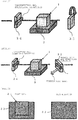
FIG. 1 is a front view and a side elevation showing a mode of a light guide body of the present invention whose one side surface alone is joined and fixed to a base; -
FIG. 2 is a schematic view showing a part of a structure in an optical module of the present invention; -
FIG. 3 is a schematic view showing a structure of a measurement system which measures an extinction ratio of the light guide body after joining and fixation; -
FIG. 4 is a schematic view showing a structure of a measurement system which measures an insertion loss, an excess loss, and backscattering of the light guide body; and -
FIG. 5 is a front view and a side elevation showing a mode of a light guide body of the present invention having three side surfaces joined and fixed to a groove of a base. - An embodiment of the present invention will now be described hereinafter, but the present invention is not restricted thereto.
- First, a light guide body according to the present invention will be described. Such a
light guide body 1 of the present invention as shown inFIG. 1 is used for optical path and optical axis adjustment. More specifically, thelight guide body 1 of the present invention is installed on an optical path in an optical module or the like, and an optical axis of light exiting from thelight guide body 1 is shifted from an optical axis of incident light by refracting the light which has entered thelight guide body 1, thereby adjusting the optical path and the optical axis. - Further, the
light guide body 1 of the present invention is a silicon light guide body made of a silicon single crystal having an extinction ratio of 30 dB or more. Since the silicon single crystal has a high refractive index, an angle at which the light is internally propagated largely varies when the light guide body is slightly tilted, an exit position of the light thereby greatly changes, thus largely shifting an optical axis. Furthermore, when the extinction ratio of the silicon single crystal constituting the light guide body is 30 dB or more, a polarization plane of the light which is transmitted through the silicon single crystal is not considerably disordered. That is, an influence of polarization dependence of circuit components which the light enters after transmission through the light guide body hardly appears, and optical characteristics can be prevented from being degraded. Thus, the light guide body of the present invention can suppress a change in polarization characteristics and then facilitate the optical path and optical axis adjustment. - It is to be noted that a shape of the light guide body made of the silicon single crystal may be appropriately set in accordance with a design of the optical module or the like in which the light guide body is arranged, and it may be a tabular or cubic shape. Additionally, antireflective coating may be applied to the
light guide body 1. - Further, the light guide body of the present invention may be joined and fixed to a base which supports the light guide body .
- The silicon single crystal having the extinction ratio of 30 dB or more can be obtained as follows, for example. First, a silicon single crystal of a predetermined size is sliced out from a silicon single crystal ingot manufactured by a general silicon single crystal manufacturing method such as a Czochralski method (a CZ method) or a floating zone method (an FZ method). Furthermore, polishing is performed in such a manner that strain to the silicon single crystal can be reduced. Since the distinction ratio of the silicon single crystal is affected by the strain to the silicon single crystal, the extinction ratio of 30 dB or more can be provided by performing the processing so as to reduce the strain.
- Moreover, the extinction ratio of the light guide body made of the silicon single crystal is also affected by joining strain to the base which supports the light guide body. Thus, as shown in
FIG. 1 , it is preferable to join and fix only one side surface of thelight guide body 1 of the present invention to thebase 3. When the one side surface alone is joined and fixed to the base, joining strain can be minimized and degradation of extinction performance can be suppressed as compared with, e.g., a case where all the circumference is joined and fixed. - It is to be noted that the extinction ratio of the silicon single crystal is a ratio of "intensity Imax of linearly polarized light in a polarizing direction of a polarizer" and "intensity Imin of linearly polarized light tilted at 90° from the polarizing direction of the polarizer" of the light after transmission of the light from the polarizer through the silicon single crystal, and it can defined as follows when it is converted to decibel:

- A description will now be given as to the optical module of the present invention. The optical module of the present invention includes the
light guide body 1 of the present invention installed at an installation angle adjusted for the optical path and optical axis adjustment between components A and B. In this manner, the optical module of the present invention can be subjected to the optical path and optical axis adjustment by a simple technique using thelight guide body 1 of the present invention. - It is to be noted that the components mentioned here mean compound semiconductor components such as a laser or a modulator or waveguide circuit components such as a resonator, a multiplexer, or a splitter. Additionally, any other component can be used as long as it is a component generally used in a structure of the optical module.
- Further,
FIG. 2 shows a mode in which thelight guide body 1 is installed away from the components A and B, but the present invention is not restricted to this mode alone. Adhesive coating may be applied to one end or both ends of the light guide body of the present invention, and the light guide body may be directly joined to the components A and B at an angle (a tilt gap is filled with an adhesive). - Further, in case of performing the optical path and optical axis adjustment by the light guide body of the present invention, the light used in the optical module can be particularly preferably used to light having a high transmissivity to the silicon single crystal (i.e., infrared light having a wavelength above a give level).
- A description will now be given as to the optical path and optical axis adjustment method of the present invention. According to the optical path and optical axis adjustment method of the present invention, the optical path and optical axis adjustment between components is performed by adjusting an installation angle of the light guide body of the present invention. The between components mentioned here mean a space between components generally used in a structure of the optical module. Such an optical path and optical axis adjustment method enables greatly changing an optical path by simple means, namely, just slightly tilting the light guide body, thereby adjusting the optical path. Further, since the light guide body of the present invention is used, the polarization characteristics of the light are not largely disordered.
- The present invention will now be more specifically described hereinafter with reference to examples and comparative examples of the present invention, but the present invention is not restricted thereto.
- An Si single crystal (Example 1), a garnet single crystal (Gd3Ga5O12) (Comparative Example 1), or a quartz plate (SiO2) (Comparative Example 2) was used as a light guide body, and an optical path change amount (an optical axis shift amount) corresponding to a change in installation angle of each light guide body was measured. First, a double-side AR coat to air (an anti-reflective coat) for a wavelength of 1550 nm was applied to each of the Si single crystal (Example 1), the garnet single crystal (Gd3Ga5O12) (Comparative Example 1), and the quartz plate (SiO2) (Comparative Example 2) subjected to the double-side polishing to provide a thickness of 1.5 mm, and slicing was performed to provide each chip which is 1.5 mm in height and width, whereby each light guide body was fabricated. At this time, the Si single crystal (a width of 1.5 mm × a height of 1.5 mm × a thickness of 1.5 mm) had an extinction ratio of 42 dB and an insertion loss of 0.02 dB. Furthermore, the respective light guide bodies of Example 1 and Comparative Examples 1 and 2 were tilted at 1 to 10° to incident light having a wavelength of 1550 nm, and an optical path change amount (an optical axis shift amount) corresponding to each tilt angle was measured. Consequently, as can be understood from Table 1, the light guide body using the Si single crystal having a large refractive index was able to provide an extremely larger numerical value of the optical path change amount (the optical axis shift amount) to a change amount of the installation angle than those of the respective light guide bodies using garnet and quartz.
[Table 1] Optical axis shift amount (µm) Light guide body material/angle (deg) 1 2 3 4 5 6 10 Example 1 Si single crystal 19 37 56 74 93 112 188 Comparative Example 1 Garnet (Gd3Ga5O12) 13 25 38 50 63 75 126 Comparative Example 2 Quartz (SiO2) 9 18 27 35 44 53 89 - In general, a polarization optical material or a waveguide type optical component having large polarization dependence is arranged on a rear stage. Thus, in Example 2, an influence of transmitted light transmitted through the light guide body of the present invention on the component was measured under the following conditions. First, the same silicon single crystal as that fabricated in Example 1 was joined and fixed to an SUS304 (stainless steel) plate having a width of 2.0 mm, a height of 0.5 mm, and an optical axial length of 2.0 mm by using an epoxy thermosetting type adhesive, thereby joining and fixing one side surface of such a
light guide body 1 made of a silicon single crystal as shown inFIG. 1 to abase 3. Optical characteristics of the silicon single crystal of the light guide body were measured, and then excellent values, i.e., an extinction ratio of 41 dB and an insertion loss of 0.02 dB were provided. - It is to be noted that the extinction ratio of the light guide body after the joining and the fixation was measured by using such a measurement system as shown in
FIG. 3 . First, as shown inFIG. 3 , apolarizer 34 with an extinction ratio of 50 dB and an analyzer 35 both of which have metal particles aligned therein are arranged on front and rear sides of thelight guide body 1. Further, an angle of thepolarizer 34 was fixed (a transmitting and polarizing direction is fixed), and the analyzer 35 was rotated to measure an extinction ratio. - Then, as shown in
FIG. 4 , the light transmitted through thepolarizer 34 which has the metal particles aligned therein and has extinction performance of 50 dB was allowed to enter thelight guide body 1, the analyzer 35 which likewise has metal particles aligned therein and has the extinction performance of 50 dB was arranged on a rear stage to coincide with its transmitting and polarizing direction and to tilt at 8° to an optical axis, and backscattered light from the analyzer 35 was measured. - Table 2 shows an extinction ratio and an insertion loss of each joined and fixed light guide body. Further, each excess loss at the time of transmission through the analyzer and each backscattered light amount from the analyzer are also shown. It is to be noted that the excess loss at the time of transmission through the analyzer is a value excluding an insertion loss of the analyzer. Furthermore, the backscattered light amount is a reflected light amount (a relative value) from the analyzer to an analyzer incident light amount when analyzer incident light amount is 1.
- Each light guide body was fabricated like Example 2 except that an extinction ratio of a silicon single crystal was adjusted to such a value as shown in Table 2, and the same measurement as that in Example 2 was carried out. The extinction ratio of the silicon single crystal of the light guide body was changed by adjusting a joining state of the silicon single crystal to a base and further adjusting joining strain.
- Each light guide body was fabricated like Example 2 except that an extinction ratio of the light guide body made of a silicon single crystal was adjusted to a value which is less than 30 dB as shown in Table 2, and the same measurement as that in Example 2 was carried out. In each of Comparative Examples 3 and 4, as shown in
FIG. 5 , three side surfaces of the light guide body 51 made of the silicon single crystal were joined and fixed to a base 53 (an SUS304 component) having a width of 2.0 mm, a height of 2.0 mm, and an optical axis length of 2.0 mm and also having a groove formed with a width of 1.5 mm, a depth of 1.5 mm, and an optical axis direction of 2.0 mm at a central portion thereof by using an epoxy thermosetting type adhesive. As a result of measuring optical characteristics of the light guide body of each of Comparative Examples 3 and 4, an extinction ratio was 24 to 25 dB and varied in a radial direction of a workpiece (the light guide body), and an insertion loss was 0.06 to 0.04 dB, which was higher than those in Examples 2 to 5. It can be considered that such results were obtained due to joining strain. Each extinction ratio was adjusted by adjusting the joining strain in this manner. Table 2 shows the extinction ratio of the joined and fixed light guide body, the insertion loss, an excess loss at the time of transmission through the analyzer, and a backscattered light amount from the analyzer according to each of Comparative Examples 3 and 4.[Table 2] Si light guide body Excess loss in transmission through analyzer (dB) Backscattered light amount from analyzer (%) Extinction ratio(dB) Insertion loss(dB) Example 2 41 0.02 0.002 0.001 Example 3 38 0.02 0.002 0.001 Example 4 36 0.02 0.002 0.002 Example 5 30 0.02 0.004 0.006 Comparative Example 3 25 0.04 0.017 0.030 Comparative Example 4 24 0.06 0.032 0.042 - It was found out that the insertion loss increases when the extinction ratio of each light guide body decreases, and the excess loss largely increases and the backscattered light amount also rises when the extinction ratio is less than 30 dB. It was understood that, to reduce an optical influence on each component arranged on the rear stage of the light guide body, the extinction ratio of the joined and fixed light guide body must be 30 dB or more.
- Moreover, when each light guide body fabricated in Examples and Comparative Examples mentioned above was actually inserted between a compound semiconductor component and an Si waveguide circuit component, a variation in polarization dependence characteristics was not observed in each light guide body having a large extinction ratio (30 dB or more), but a variation in polarization dependence characteristics of the waveguide circuit component was observed in each light guide body having a small extinction ratio (less than 30 dB). The compound semiconductor component (e.g., a laser) has polarization properties of 25 dB or more, and inserting the workpiece having the low extinction ratio between the optical paths impaired the polarization properties.
- It is to be noted that the present invention is not restricted to the foregoing embodiment. The foregoing embodiment is an illustrative example, and any example which has substantially the same structure and exerts the same functions and effects as the technical concept described in claims of the present invention is included in the technical scope of the present invention.
Claims (4)
- A light guide body for optical path and optical axis adjustment,
the light guide body comprising a silicon single crystal having an extinction ratio of 30 dB or more. - The light guide body according to claim 1,
wherein one side surface alone of the light guide body is joined and fixed to a base. - An optical module comprising a light guide body according to claim 1 or 2 installed at an installation angle adjusted for optical path and optical axis adjustment between components.
- An optical path and optical axis adjustment method comprising adjusting an installation angle of a light guide body according to claim 1 or 2 to perform the optical path and optical axis adjustment between components.
Applications Claiming Priority (2)
| Application Number | Priority Date | Filing Date | Title |
|---|---|---|---|
| JP2016171806A JP6694652B2 (en) | 2016-09-02 | 2016-09-02 | Optical module and optical path optical axis adjusting method |
| PCT/JP2017/029332 WO2018043109A1 (en) | 2016-09-02 | 2017-08-15 | Light guide body, optical module, and method for adjusting optical axis of optical path |
Publications (2)
| Publication Number | Publication Date |
|---|---|
| EP3508898A1 true EP3508898A1 (en) | 2019-07-10 |
| EP3508898A4 EP3508898A4 (en) | 2020-04-22 |
Family
ID=61300599
Family Applications (1)
| Application Number | Title | Priority Date | Filing Date |
|---|---|---|---|
| EP17846117.4A Pending EP3508898A4 (en) | 2016-09-02 | 2017-08-15 | LIGHT GUIDING BODY, OPTICAL MODULE AND OPTICAL AXIS ADJUSTMENT METHOD |
Country Status (5)
| Country | Link |
|---|---|
| US (1) | US11143829B2 (en) |
| EP (1) | EP3508898A4 (en) |
| JP (1) | JP6694652B2 (en) |
| CN (1) | CN109642988B (en) |
| WO (1) | WO2018043109A1 (en) |
Families Citing this family (1)
| Publication number | Priority date | Publication date | Assignee | Title |
|---|---|---|---|---|
| JP7811903B2 (en) | 2022-12-28 | 2026-02-06 | 信越化学工業株式会社 | Optical isolator and method for manufacturing the same |
Family Cites Families (26)
| Publication number | Priority date | Publication date | Assignee | Title |
|---|---|---|---|---|
| US4134785A (en) * | 1977-04-13 | 1979-01-16 | Western Electric Company, Inc. | Real-time analysis and control of melt-chemistry in crystal growing operations |
| DK371977A (en) * | 1977-08-22 | 1979-02-23 | Topsil As | METHOD AND APPLIANCE FOR REFINING SALMON MATERIAL |
| US4532000A (en) * | 1983-09-28 | 1985-07-30 | Hughes Aircraft Company | Fabrication of single crystal fibers from congruently melting polycrystalline fibers |
| JPH07301742A (en) * | 1994-05-06 | 1995-11-14 | Nikon Corp | camera |
| JPH07301724A (en) | 1994-05-09 | 1995-11-14 | Nippon Sheet Glass Co Ltd | Light beam incident device with incident position adjusting mechanism |
| US6211993B1 (en) * | 1996-05-20 | 2001-04-03 | Nz Applied Technologies Corporation | Thin film ferroelectric light modulators |
| JPH11352348A (en) * | 1998-06-05 | 1999-12-24 | Nippon Telegr & Teleph Corp <Ntt> | Optical waveguide polarizer |
| US6981804B2 (en) * | 1998-06-08 | 2006-01-03 | Arrayed Fiberoptics Corporation | Vertically integrated optical devices coupled to optical fibers |
| JP2000249834A (en) | 1999-03-01 | 2000-09-14 | Kyocera Corp | Polarizer and method of manufacturing the same |
| US6374009B1 (en) * | 1999-05-10 | 2002-04-16 | Jds Uniphase Corporation | TEMC fiber based optical switch |
| JP3613200B2 (en) * | 2000-09-01 | 2005-01-26 | 住友電気工業株式会社 | Optical module |
| DE10143781B4 (en) * | 2001-08-31 | 2004-11-18 | Infineon Technologies Ag | Method for coupling a surface-oriented opto-electronic component with an optical fiber and opto-electronic component for carrying out such a method |
| US6834152B2 (en) | 2001-09-10 | 2004-12-21 | California Institute Of Technology | Strip loaded waveguide with low-index transition layer |
| JP2004272143A (en) * | 2003-03-12 | 2004-09-30 | Oyokoden Lab Co Ltd | Optical coupling device for optical waveguide and its manufacturing method |
| JP2004347702A (en) | 2003-05-20 | 2004-12-09 | Sumitomo Electric Ind Ltd | Optical module, optical communication system, and optical axis adjustment device |
| JP2007010854A (en) * | 2005-06-29 | 2007-01-18 | Nec Corp | Module for optical communication using parallel flat plate for optical axis compensation, and manufacturing method of same |
| JP4522340B2 (en) * | 2005-08-01 | 2010-08-11 | シャープ株式会社 | Planar waveguide element |
| JP2008111863A (en) * | 2006-10-27 | 2008-05-15 | Kyocera Corp | Optical multiplexer / demultiplexer and optical transmitter / receiver using the same |
| JP2009020275A (en) * | 2007-07-11 | 2009-01-29 | Oki Electric Ind Co Ltd | Optical communication module |
| JP2010020285A (en) * | 2008-03-28 | 2010-01-28 | Panasonic Corp | Laser light source, image display device and processing apparatus |
| CN101833182B (en) | 2010-04-13 | 2011-07-27 | 友达光电股份有限公司 | Panel display module with reinforced structure and manufacturing method thereof |
| CN101833172B (en) | 2010-06-13 | 2011-10-05 | 中南大学 | Method for coupling and splitting polarized light and coupling splitting device |
| JP5546410B2 (en) * | 2010-10-07 | 2014-07-09 | アルプス電気株式会社 | Optical member, optical communication module using the same, and alignment method |
| US9499921B2 (en) * | 2012-07-30 | 2016-11-22 | Rayton Solar Inc. | Float zone silicon wafer manufacturing system and related process |
| US8837870B1 (en) * | 2013-04-29 | 2014-09-16 | Photop Technologies, Inc. | Fiber coupled laser device having high polarization extinction ratio and high stability |
| JP2015225252A (en) * | 2014-05-28 | 2015-12-14 | 株式会社フジクラ | Substrate-type waveguide device and optical modulator |
-
2016
- 2016-09-02 JP JP2016171806A patent/JP6694652B2/en active Active
-
2017
- 2017-08-15 EP EP17846117.4A patent/EP3508898A4/en active Pending
- 2017-08-15 WO PCT/JP2017/029332 patent/WO2018043109A1/en not_active Ceased
- 2017-08-15 US US16/327,030 patent/US11143829B2/en not_active Expired - Fee Related
- 2017-08-15 CN CN201780053254.1A patent/CN109642988B/en active Active
Also Published As
| Publication number | Publication date |
|---|---|
| US20200183102A1 (en) | 2020-06-11 |
| CA3034603A1 (en) | 2018-03-08 |
| US11143829B2 (en) | 2021-10-12 |
| EP3508898A4 (en) | 2020-04-22 |
| CN109642988B (en) | 2023-08-29 |
| JP2018036594A (en) | 2018-03-08 |
| WO2018043109A1 (en) | 2018-03-08 |
| CN109642988A (en) | 2019-04-16 |
| JP6694652B2 (en) | 2020-05-20 |
Similar Documents
| Publication | Publication Date | Title |
|---|---|---|
| US6310720B1 (en) | Polarization insensitive semiconductor optical amplifier | |
| EP3314320B1 (en) | Mode converter with a s-bent taper and related polarization rotator | |
| US20210041636A1 (en) | Optical receptacle and optical transceiver | |
| US10613339B2 (en) | Collimation lens and optical module | |
| US7412132B1 (en) | Mini fiber optic isolator | |
| JP2006208929A (en) | Optical power monitor and its manufacturing method | |
| CN100516969C (en) | Embedded Optical Irreversible Loop Device | |
| US7693372B2 (en) | Optical communication module using refraction plate for optical axis compensation, and manufacturing method of the same | |
| US4966444A (en) | Feedback-free optical arrangement for converting polarized laser emissions into a convergent beam | |
| US11143829B2 (en) | Light guide body, optical module, and optical path and optical axis adjustment method | |
| EP1612588B1 (en) | Optical isolator with tilted optical isolator element | |
| JP2003131050A (en) | Optical fiber coupling system | |
| CA3034603C (en) | Light guide body, optical module, and optical path and optical axis adjustment method | |
| US20210026080A1 (en) | Optical receptacle and optical transceiver | |
| CA2333456A1 (en) | Assembly of optical component and optical fibre | |
| US7729580B2 (en) | Waveguide type optical device and manufacturing method of the waveguide type optical device | |
| US20040114862A1 (en) | Optical module using gradient index rod lens | |
| Riveros et al. | Optical grating coupling on silicon photonics based on metallized angle-polished fibers | |
| JP2989979B2 (en) | Optical isolator | |
| US6744952B2 (en) | Connecting device for connecting at least two optical waveguides, in particular optical waveguides of different refractive index | |
| US20020012515A1 (en) | High reliability, fixed attenuator | |
| JP4812342B2 (en) | Optical connector | |
| JP2006276507A (en) | Faraday rotating mirror | |
| CN120143470A (en) | Low-loss deep ultraviolet cross polarization prism | |
| US20110038046A1 (en) | Non-reciprocal unit used for polarization dependent type optical isolator and polarization dependent type optical isolator |
Legal Events
| Date | Code | Title | Description |
|---|---|---|---|
| STAA | Information on the status of an ep patent application or granted ep patent |
Free format text: STATUS: THE INTERNATIONAL PUBLICATION HAS BEEN MADE |
|
| PUAI | Public reference made under article 153(3) epc to a published international application that has entered the european phase |
Free format text: ORIGINAL CODE: 0009012 |
|
| STAA | Information on the status of an ep patent application or granted ep patent |
Free format text: STATUS: REQUEST FOR EXAMINATION WAS MADE |
|
| 17P | Request for examination filed |
Effective date: 20190219 |
|
| AK | Designated contracting states |
Kind code of ref document: A1 Designated state(s): AL AT BE BG CH CY CZ DE DK EE ES FI FR GB GR HR HU IE IS IT LI LT LU LV MC MK MT NL NO PL PT RO RS SE SI SK SM TR |
|
| AX | Request for extension of the european patent |
Extension state: BA ME |
|
| DAV | Request for validation of the european patent (deleted) | ||
| DAX | Request for extension of the european patent (deleted) | ||
| A4 | Supplementary search report drawn up and despatched |
Effective date: 20200323 |
|
| RIC1 | Information provided on ipc code assigned before grant |
Ipc: G02B 6/00 20060101ALI20200317BHEP Ipc: G02B 6/126 20060101ALI20200317BHEP Ipc: G02B 6/26 20060101AFI20200317BHEP Ipc: G02B 6/42 20060101ALI20200317BHEP Ipc: G02B 5/30 20060101ALI20200317BHEP |
|
| STAA | Information on the status of an ep patent application or granted ep patent |
Free format text: STATUS: EXAMINATION IS IN PROGRESS |
|
| 17Q | First examination report despatched |
Effective date: 20220103 |
|
| RAP3 | Party data changed (applicant data changed or rights of an application transferred) |
Owner name: SHIN-ETSU CHEMICAL CO., LTD. |