EP3508039B1 - Circuits and methods providing mutual capacitance in vertical electrical connections - Google Patents
Circuits and methods providing mutual capacitance in vertical electrical connections Download PDFInfo
- Publication number
- EP3508039B1 EP3508039B1 EP17754922.7A EP17754922A EP3508039B1 EP 3508039 B1 EP3508039 B1 EP 3508039B1 EP 17754922 A EP17754922 A EP 17754922A EP 3508039 B1 EP3508039 B1 EP 3508039B1
- Authority
- EP
- European Patent Office
- Prior art keywords
- electrical
- electrical connection
- vertical
- capacitive structure
- layer
- Prior art date
- Legal status (The legal status is an assumption and is not a legal conclusion. Google has not performed a legal analysis and makes no representation as to the accuracy of the status listed.)
- Active
Links
Images


Classifications
-
- G—PHYSICS
- G11—INFORMATION STORAGE
- G11C—STATIC STORES
- G11C11/00—Digital stores characterised by the use of particular electric or magnetic storage elements; Storage elements therefor
- G11C11/21—Digital stores characterised by the use of particular electric or magnetic storage elements; Storage elements therefor using electric elements
- G11C11/34—Digital stores characterised by the use of particular electric or magnetic storage elements; Storage elements therefor using electric elements using semiconductor devices
- G11C11/40—Digital stores characterised by the use of particular electric or magnetic storage elements; Storage elements therefor using electric elements using semiconductor devices using transistors
- G11C11/401—Digital stores characterised by the use of particular electric or magnetic storage elements; Storage elements therefor using electric elements using semiconductor devices using transistors forming cells needing refreshing or charge regeneration, i.e. dynamic cells
-
- H—ELECTRICITY
- H05—ELECTRIC TECHNIQUES NOT OTHERWISE PROVIDED FOR
- H05K—PRINTED CIRCUITS; CASINGS OR CONSTRUCTIONAL DETAILS OF ELECTRIC APPARATUS; MANUFACTURE OF ASSEMBLAGES OF ELECTRICAL COMPONENTS
- H05K1/00—Printed circuits
- H05K1/02—Details
- H05K1/0213—Electrical arrangements not otherwise provided for
- H05K1/0216—Reduction of cross-talk, noise or electromagnetic interference
- H05K1/0228—Compensation of cross-talk by a mutually correlated lay-out of printed circuit traces, e.g. for compensation of cross-talk in mounted connectors
-
- H—ELECTRICITY
- H05—ELECTRIC TECHNIQUES NOT OTHERWISE PROVIDED FOR
- H05K—PRINTED CIRCUITS; CASINGS OR CONSTRUCTIONAL DETAILS OF ELECTRIC APPARATUS; MANUFACTURE OF ASSEMBLAGES OF ELECTRICAL COMPONENTS
- H05K1/00—Printed circuits
- H05K1/02—Details
- H05K1/11—Printed elements for providing electric connections to or between printed circuits
- H05K1/115—Via connections; Lands around holes or via connections
- H05K1/116—Lands, clearance holes or other lay-out details concerning the surrounding of a via
-
- H—ELECTRICITY
- H10—SEMICONDUCTOR DEVICES; ELECTRIC SOLID-STATE DEVICES NOT OTHERWISE PROVIDED FOR
- H10B—ELECTRONIC MEMORY DEVICES
- H10B12/00—Dynamic random access memory [DRAM] devices
-
- H—ELECTRICITY
- H10—SEMICONDUCTOR DEVICES; ELECTRIC SOLID-STATE DEVICES NOT OTHERWISE PROVIDED FOR
- H10D—INORGANIC ELECTRIC SEMICONDUCTOR DEVICES
- H10D1/00—Resistors, capacitors or inductors
-
- H—ELECTRICITY
- H10—SEMICONDUCTOR DEVICES; ELECTRIC SOLID-STATE DEVICES NOT OTHERWISE PROVIDED FOR
- H10D—INORGANIC ELECTRIC SEMICONDUCTOR DEVICES
- H10D1/00—Resistors, capacitors or inductors
- H10D1/60—Capacitors
- H10D1/68—Capacitors having no potential barriers
-
- H—ELECTRICITY
- H10—SEMICONDUCTOR DEVICES; ELECTRIC SOLID-STATE DEVICES NOT OTHERWISE PROVIDED FOR
- H10W—GENERIC PACKAGES, INTERCONNECTIONS, CONNECTORS OR OTHER CONSTRUCTIONAL DETAILS OF DEVICES COVERED BY CLASS H10
- H10W70/00—Package substrates; Interposers; Redistribution layers [RDL]
- H10W70/60—Insulating or insulated package substrates; Interposers; Redistribution layers
- H10W70/62—Insulating or insulated package substrates; Interposers; Redistribution layers characterised by their interconnections
- H10W70/63—Vias, e.g. via plugs
- H10W70/635—Through-vias
-
- H—ELECTRICITY
- H10—SEMICONDUCTOR DEVICES; ELECTRIC SOLID-STATE DEVICES NOT OTHERWISE PROVIDED FOR
- H10W—GENERIC PACKAGES, INTERCONNECTIONS, CONNECTORS OR OTHER CONSTRUCTIONAL DETAILS OF DEVICES COVERED BY CLASS H10
- H10W70/00—Package substrates; Interposers; Redistribution layers [RDL]
- H10W70/60—Insulating or insulated package substrates; Interposers; Redistribution layers
- H10W70/67—Insulating or insulated package substrates; Interposers; Redistribution layers characterised by their insulating layers or insulating parts
- H10W70/68—Shapes or dispositions thereof
- H10W70/685—Shapes or dispositions thereof comprising multiple insulating layers
-
- H—ELECTRICITY
- H10—SEMICONDUCTOR DEVICES; ELECTRIC SOLID-STATE DEVICES NOT OTHERWISE PROVIDED FOR
- H10W—GENERIC PACKAGES, INTERCONNECTIONS, CONNECTORS OR OTHER CONSTRUCTIONAL DETAILS OF DEVICES COVERED BY CLASS H10
- H10W72/00—Interconnections or connectors in packages
-
- G—PHYSICS
- G11—INFORMATION STORAGE
- G11C—STATIC STORES
- G11C7/00—Arrangements for writing information into, or reading information out from, a digital store
- G11C7/02—Arrangements for writing information into, or reading information out from, a digital store with means for avoiding parasitic signals
-
- H—ELECTRICITY
- H05—ELECTRIC TECHNIQUES NOT OTHERWISE PROVIDED FOR
- H05K—PRINTED CIRCUITS; CASINGS OR CONSTRUCTIONAL DETAILS OF ELECTRIC APPARATUS; MANUFACTURE OF ASSEMBLAGES OF ELECTRICAL COMPONENTS
- H05K1/00—Printed circuits
- H05K1/02—Details
- H05K1/0213—Electrical arrangements not otherwise provided for
- H05K1/0216—Reduction of cross-talk, noise or electromagnetic interference
-
- H—ELECTRICITY
- H05—ELECTRIC TECHNIQUES NOT OTHERWISE PROVIDED FOR
- H05K—PRINTED CIRCUITS; CASINGS OR CONSTRUCTIONAL DETAILS OF ELECTRIC APPARATUS; MANUFACTURE OF ASSEMBLAGES OF ELECTRICAL COMPONENTS
- H05K1/00—Printed circuits
- H05K1/16—Printed circuits incorporating printed electric components, e.g. printed resistors, capacitors or inductors
- H05K1/162—Printed circuits incorporating printed electric components, e.g. printed resistors, capacitors or inductors incorporating printed capacitors
-
- H—ELECTRICITY
- H05—ELECTRIC TECHNIQUES NOT OTHERWISE PROVIDED FOR
- H05K—PRINTED CIRCUITS; CASINGS OR CONSTRUCTIONAL DETAILS OF ELECTRIC APPARATUS; MANUFACTURE OF ASSEMBLAGES OF ELECTRICAL COMPONENTS
- H05K2201/00—Indexing scheme relating to printed circuits covered by H05K1/00
- H05K2201/09—Shape and layout
- H05K2201/09209—Shape and layout details of conductors
- H05K2201/095—Conductive through-holes or vias
- H05K2201/09636—Details of adjacent, not connected vias
Definitions
- the present application relates, generally, to crosstalk reduction, and more specifically to circuits and methods using mutual capacitance to reduce or minimize crosstalk.
- a conventional computing device may include a chip disposed in a package, where the package is mounted upon a printed circuit board (PCB).
- the chip includes a multi-core processor, which is disposed within a chip package.
- the chip package includes socket pins, which are coupled with electrical contacts on the printed circuit board. Traces on the printed circuit board provide electrical communication between the multi-core processor and random-access memory chips.
- the chip/package/PCB structure includes vertical electrical connections. For instance, metal vias within the chip itself allow for communication between different metal layers. Similarly, vias within the printed circuit board allow for communication between different layers of the PCB.
- US 2013/279134 A1 describing first and second signal wiring patterns formed in a first conductor layer.
- a first electrode pad electrically connected to the first signal wiring pattern through a first via and a second electrode pad electrically connected to the second signal wiring pattern through a second via are formed in a second conductor layer as a surface layer.
- a third conductor layer is disposed between the first conductor layer and the second conductor layer with an insulator interposed between those conductor layers.
- a first pad electrically connected to the first via is formed in the third conductor layer.
- the first pad includes an opposed portion which overlaps the second electrode pad as viewed in a direction perpendicular to the surface of a printed board and which is opposed to the second electrode pad through intermediation of the insulator. This enables reduction of crosstalk noise caused between the signal wirings.
- US 2005/191785 A1 describing a substrate for a package of high frequency semiconductor devices comprising a planar insulating substrate having a plurality of parallel, planar metal layers embedded in the insulator.
- the substrate further has at least one pair of parallel, metal-filled vias traversing the substrate; the vias have a diameter and a distance from each other of at least this diameter.
- the metal in each via has a sheet-like extension in each of selected planes of said metal layers, resulting in an increased via-to-via capacitance so that the reflection of a high frequency signal is less than 10%.
- the connector includes a first compensation structure provided on an inner metalized layer of the PCB at a first stage area of the PCB, and a second compensation structure, provided at a second stage area of the PCB, for increasing compensation capacitance with increasing frequency.
- Various embodiments include systems and methods to reduce far end crosstalk by addressing mutual capacitance of vertical electrical connections, such as vias.
- Vias may include capacitive structures that serve to increase mutual capacitance among adjacent vias, thereby reducing far end crosstalk voltage levels.
- V Fext is a magnitude of far end crosstalk
- C m is mutual capacitance between two structures
- L m is mutual inductance between those two structures
- C s and L s are self-capacitance and self-inductance respectively.
- V agg is a voltage of an aggressor signal
- t pd is a propagation delay of the signal.
- mutual inductance L m tends to dominate and thus, causing negative far end crosstalk.
- mutual inductance L m , self-capacitance C s , and self-inductance L s tend to be uncontrollable in tighter vertical sections.
- mutual capacitance C m can be increased in order to reduce the value of(C m / C s - L m / L s ).
- an electrical device in one embodiment, includes a system on chip (SOC) disposed within a chip package, wherein the chip package is disposed upon a printed circuit board.
- the printed circuit board is made of a plurality of dielectric layers, and conductive features, such as traces and contacts, are disposed on various ones of the dielectric layers.
- electrical signals to and from the SOC are conducted through the chip package and to the printed circuit board by virtue of socket pins.
- the socket pins are in electrical communication with conductive contacts built on a top layer of the printed circuit board. Some of the electrical contacts are further in electrical communication with vias within the PCB.
- the PCB includes electrical traces from ones of the vias across a horizontal distance to a second set of vias.
- the second set of vias are in electrical communication with contacts on the top layer of the PCB and with a memory chip or a connector which holds a dual in-line memory module (DIMM) with memory chip on it.
- DIMM dual in-line memory module
- the SOC reads and writes data to and from the memory chip, it conducts signals to ones of its vias, and from the vias to the traces and to the second set of vias and to the memory chip.
- the memory chip also includes driver circuits that drive signals to and from the SOC along the same or similar routes.
- An example of a memory chip includes a double data rate fourth-generation synchronous dynamic random-access memory (DDR4), although the scope of embodiments is not limited to any particular memory technology.
- DDR4 double data rate fourth-generation synchronous dynamic random-access memory
- each of the adjacent vias may include capacitive structures within a layer of the PCB below the top layer.
- the capacitive structures are formed in a plane perpendicular to the vertical dimensions of the vias, and the capacitive structures extend toward each other in their own length dimensions. While the top layer of the PCB may be used for electrical contacts, other layers of the PCB may be available for hosting the capacitive structures.
- the shapes of the capacitive structures increase mutual capacitance of the two adjacent vias, thereby mitigating far end crosstalk according to Equation 1.
- the shapes of the structures may be chosen through simulation or experimentation to achieve a desired level of mutual capacitance at the particular signal frequencies.
- the concept of including capacitive structures on vias may be applied to vias within the SOC or vias within the chip package. In fact, such capacitive structures may be applied to any appropriate vertical electrical connection.
- inventions include methods of use for electrical devices having a structure similar to the above, where conduction of the signals stores energy within an electric field between capacitive structures, thereby reducing far end crosstalk.
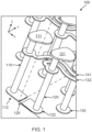
- Figure 1 is a simplified isometric diagram illustrating an example electrical device 100 in which various embodiments may be implemented.
- Figure 1 includes a legend illustrating the X, Y, and Z axes.
- the Z axis defines the vertical dimension of the vias 110 and 120.
- the vias 110 and 120 are implemented in a PCB in this example; however, the PCB itself is not illustrated to avoid obscuring the view of the vias 110 and 120. Nonetheless, one of skilled in the art should readily appreciate that the PCB includes a plurality of layers of dielectric material, where each of the layers extends in a plane defined by the X and Y axes.
- An example of a PCB includes dielectric layers of FR-4 glass epoxy or other suitable material.
- the vias 110, 120 and other conductive and capacitive structures may be made of copper and/or other appropriate conductor.
- Via 110 has a pad 111 to provide electrical coupling with a package socket pin (not shown).
- Pad 111 is disposed on a top layer of the PCB.
- Via 120 has a similar pad 121, also disposed on the top layer of the PCB.
- Capacitive structures 112, 122 are provided in the embodiment of Figure 1 in order to increase mutual capacitance. Specifically, the surface areas of capacitive structures 112, 122 are increased compared with via pad 130. In this example capacitive structures 112, 122 are coplanar and are disposed on a single layer of the PCB structure - in this example, the bottom layer of the PCB structure.
- capacitive structures 112, 122 each have a major dimension in the x-axis and extend toward each other in the x-axis, but do not make electrical contact with each other. Capacitive structures 112, 122 do not provide direct electrical contact to another structure, but rather are electrically isolated from structures other than their respective vias 110, 120.
- the shapes of capacitive structures 112, 122 is partially semicircular with elongated rectangular portions extending along the x-axis toward each other.
- the scope of embodiments may include any appropriate shape to achieve a desired value for mutual capacitance.
- far end crosstalk is a function of the signal rise time.
- signal rise time is approximately 50-100 ps
- operating voltage is 400-800 mV.
- Each of the vias 110, 120 are spaced apart by about 1 mm center-to-center, and the size of the gap 125 is approximately 100 ⁇ m.
- the capacitive structures 112, 122 form a co-planar parallel plate capacitor that stores energy in an electric field as the vias 110, 120 conduct the signals. Examples of signals include data signals and also clock signals.
- An PCB includes 18 layers of FR-4 material stacked on top of each other in the Z axis. The specific values given above are for example only, and it is understood that various embodiments may be designed as appropriate to achieve a desired value for mutual capacitance.
- Vias 110, 120 are in electrical communication with horizontal traces 131, 132 respectively.
- electrical contact pads 111, 121 receive electrical signals from an SOC (not shown) and propagate those signals along horizontal traces 131, 132 to a second set of vias (not shown) associated with a memory chip.
- capacitive structures 112, 122 are disposed in a layer of the PCB that is different from the layer used for the horizontal traces 131, 132 and different from the layer used for contact pads 111, 121.
- Various embodiments may dispose capacitive structures 112, 122 in any appropriate layer.
- the example of Figure 1 shows capacitive structures associated with only two vias 110, 120, it is understood that various embodiments may implement capacitive structures with any appropriate vias and with any appropriate number of vias.
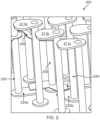
- Figure 2 is an isometric view of electrical device 200, adapted according to one aspect useful for the understanding of the invention not corresponding to the claims.
- Electrical device 200 includes capacitive structures 210 and 220, which are disposed in different layers of the PCB.
- capacitive structures 220 are similar in shape to capacitive structures 112, 122 of the example of Figure 1 .
- capacitive structures 220 are formed in a bottom-most layer of the PCB, whereas capacitive structure 210 is formed in a layer above that bottom-most layer.
- Capacitive structures 220 in their respective major dimensions within an X-Y plane, extend toward adjacent via 250.
- Capacitive structure 210 is formed as plates that extend orthogonally from the via 250 and toward adjacent vias 230, 240 in a different X-Y plane.
- Capacitive structures 210 and 220 also work to increase mutual capacitance and thereby decrease inductive crosstalk.
- the capacitive structure 220a associated with via 230 increases mutual capacitance with via 250 by forming a parallel plate capacitor with the arm of structure 210 that extends toward via 230.
- the capacitive structure 220b associated with via 240 increases mutual capacitance with via 250 by forming a parallel plate capacitor with the arm of structure 210 that extends toward via 240.
- vias 230-250 may be made of copper or other appropriate conductor and have a vertical dimension along the z-axis, whereas the layers of the PCB (not shown) are in different X-Y planes stacked along the z-axis.
- Horizontal trace 260 provide electrical coupling between via 230 and another via (not shown).
- Contact pads 211 are similar to pads 111, 121 of the embodiment of Figure 1 .
- FIG. 3 is an isometric illustration of an example electrical device 300, adapted according to one aspect.
- the electrical device 300 includes vias 330 and 340.
- Vias 330 and 340 include contact pads 311, similar to contact pads 111 and 121 of Figure 1 .
- horizontal traces 350 and 360 conduct signals from vias 330 and 340 respectively to a second subset of vias (not shown).
- the vertical dimensions of vias 330 and 340 is along the z-axis, and the layers of the PCB (not shown) are formed in X-Y planes stacked in the z-axis.
- Capacitive structures 310 and 320 are formed as circular pads having short traces extending toward the adjacent via.
- structure 310 is formed in a different layer than is structure 320.
- the scope of aspects useful for the understanding of the invention not corresponding to the claims may include structures 310 and 320 being formed in a same layer.
- structures 310 and 320 operate to increase mutual capacitance by storing energy in an electric field between the horizontal traces of structures 310 and 320.
- capacitive structures 310 and 320 are formed in different layers than are horizontal traces 350 and 360 and contact pads 311. In other words, capacitive structures 310 and 320 are formed in a layer below the topmost layer of the PCB and those layers are not used for conducting electrical signals, at least with respect to vias 330 and 340.
- the amount of mutual capacitance provided by the capacitive structures can be adjusted in the design phase by either increasing or decreasing a surface area of a respective capacitive structure. As a general rule, a greater surface area of a structure leads to a greater mutual capacitance provided by that structure. Additionally, the amount of mutual capacitance provided by the capacitive structures in Figures 1-3 may be adjusted in the design phase by increasing or decreasing a distance between capacitive structures, so that a shorter distance generally increases mutual capacitance. Also, while the embodiments shown above are described with respect to PCBs, the scope of embodiments may include vertical electrical connectors implemented elsewhere, such as in a semiconductor chip itself, in the package, or at any other appropriate place.
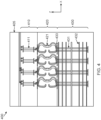
- FIG 4 is an illustration of an example device stack 400, adapted according to one embodiment.
- Device stack 400 is an example of an environment in which the structures described above with respect to Figures 1-3 may be implemented.
- Semiconductor die 405 may include a SOC or other processing device or may include a memory chip. Although not shown herein, it is understood that semiconductor die 405 may include vias vertically connecting one or more metal layers within the die itself.
- Semiconductor die 405 is disposed on a semiconductor die package 410.
- Semiconductor die package 410 provides mechanical support and electrical connections to the die 405. Examples of materials of package 410 may include plastic, ceramic, or a dielectric such as FR-4 arranged in multiple layers.
- Figure 4 shows multiple vias, exemplified by via 411.
- Via 411 provides electrical coupling between one or more contacts (not shown) on the underside of die 405 and the socket pins within the socket 420.
- Pin 421 is an example of a socket pin of socket 420.
- the socket 420 is part of the package, whereas in other embodiments it may be a physically separate component. In any event, the package 410 and the socket 420 provide electrical coupling between the semiconductor die 405 and the printed circuit board 430.
- the socket 420 is mounted to the printed circuit board 430 so that the socket pins, such as socket pin 421, are coupled to contact pads, such as contact pad 433.
- Examples of contact pads in the embodiments of Figures 1-3 include those contact pads 111, 121, 211 and 311.
- Figure 4 shows multiple vias, of which via 431 is an example.
- PCB 430 includes multiple metal layers, exemplified by metal layer 432. Each of the metal layers is disposed upon a respective dielectric layer, where PCB 430 is made up of a plurality of dielectric layers.
- the vias of PCB 430 allow for electrical signals to be passed from one layer of the PCB to another layer of the PCB, for example, by using horizontal traces.
- FIG. 4 The illustration of Figure 4 is a cutaway in the Z-X plane, so that the metal layers are shown edge-on. It is within these metal layers that the capacitive structures may be implemented. It is understood that in the edge-on view provided by Figure 4 , capacitive structures are not necessarily discernible from horizontal traces, though the illustrations of Figures 1-3 provide illustrations of how various examples may be implemented within the metal layers of PCB 430.
- Figures 1-3 describe vias and capacitive structures within the metal layers of the PCB, such as PCB 430.
- other embodiments may implement similar capacitive structures in the vias (e.g., 411) of the package 410 or vias within the semiconductor die 405.
- a designer may iteratively change shapes of capacitive structures and distances between capacitive structures to achieve a desired level of mutual capacitance.
- the shapes and distances described above with respect to Figures 1-3 are examples for specific structural dimensions and signal rise times, and those shapes and distances may be modified as appropriate to benefit different structures and different rise times.
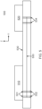
- FIG. 5 is an illustration of internal components 500 of a computing device, such as a smart phone , tablet computer, or a server mainboard, adapted according to one embodiment.
- Chip package 510 includes an SOC
- chip package 510 is mounted to PCB 530.
- chip package 520 includes a memory chip
- chip package 520 is also mounted to PCB 530.
- the SOC (not shown) is in electrical communication with vertical electrical connectors of the chip package 510 and with the PCB 530 as explained above with respect to Figure 4 .
- a memory chip (not shown) is in electrical communication with vertical electrical connectors of the chip package 520 and with the PCB 530.
- PCB 530 includes vias 531, which are in electrical communication with chip package 510.
- PCB 530 also includes vias 534, which are in electrical communication with chip package 520.
- Vias 531 are electrically coupled to vias 534 by horizontal traces 533.
- Figure 5 provides an end-on view, so that horizontal traces 533 are represented by a single line, but it is understood that vias 531 may be connected to vias 534 using multiple and separate horizontal traces.
- the SOC and the memory chip communicate by virtue of the vias 531, the horizontal traces 533, and the vias 534 according to protocols associated with DDR4, fifth-generation synchronous dynamic random-access memory (DDR5), or other appropriate technique.
- DDR5 fifth-generation synchronous dynamic random-access memory
- vias 531 include capacitive structures 532, which are similar to capacitive structures 112 and 122 of Figure 1 .
- capacitive structures of other embodiments such as those of Figures 2 and 3 , may be implemented in PCB 530 additionally or alternatively.
- the computing device may include other components, such as a battery, other printed circuit boards, other integrated circuit chips and the chip packages, and the like.
- the battery, the printed circuit boards, and the integrated circuit chips are disposed within the computing device so that they are enclosed within a physical housing of the computing device.
- the capacitive structures themselves do not make direct electrical contact to other structures and may therefore take any of a variety of arbitrary shapes that may be optimized for achieving a particular value of mutual capacitance. Furthermore, the shapes and designs of the capacitive structures may be efficiently determined using simulation software in an iterative manner, including adjusting and simulating repeatedly until acceptable parameters are found.
- FIG. 6 A flow diagram of an example method 600 of transmitting an electrical signal is illustrated in Figure 6 .
- method 600 is performed during use of an electrical device, such as those illustrated in Figures 1-5 .
- the electrical device conducts an electrical signal in a first vertical electrical connection.
- An example of an electrical signal may include a data signal or a clock signal.
- the electrical signal includes some portions that are at one voltage in some portions that are at another voltage, thereby representing digital ones and zeros.
- a clock signal may be periodic and alternating
- a data signal may include multiple instances of the same values in a row.
- the electrical signal is single-ended rather than differential, thereby making it more prone to crosstalk phenomena.
- far end crosstalk may be mitigated using the structures and techniques described herein.
- An example of action 610 includes conducting an electrical signal from one of the vias 531 to another one of the vias 534 (or vice versa) over horizontal traces 533 and Figure 5 .
- the via itself provides for communication of the electrical signal from one layer in the structure (e.g., PCB, package, a semiconductor die) to another layer in the structure.
- the electrical signal is communicated to via 531 at a top layer of the PCB 530 and is conducted along the horizontal trace 533 at a lower layer of the PCB 530. Conduction of the signal however may create crosstalk between the respective vias 531.
- the first vertical electrical connection and a second vertical electrical connection store energy in an electrical field by mutual capacitance.
- vias 531 include capacitive structures 532.
- the capacitive structures 532 add mutual capacitance between the two particular vias 531.
- the capacitive structures may increase the mutual capacitance so as to reduce or cancel far end crosstalk in accordance with Equation 1.
- a computing device may conduct millions or billions of digital bits per second from one chip to another chip by use of the vertical electrical connections and horizontal traces. Accordingly, a computing device may perform actions 610 and 620 repeatedly and at a frequency associated with the clock frequency of the chips.
- chips include a processing chip, such as an SOC, and a memory chip communicating using DDR4 or other techniques.
- method 600 is not intended to imply that actions 610 and 620 are performed in series; rather, it is understood that they occur at substantially the same time in operating examples.
Landscapes
- Engineering & Computer Science (AREA)
- Microelectronics & Electronic Packaging (AREA)
- Physics & Mathematics (AREA)
- Electromagnetism (AREA)
- Computer Hardware Design (AREA)
- Production Of Multi-Layered Print Wiring Board (AREA)
- Power Engineering (AREA)
- Electrotherapy Devices (AREA)
- Geometry (AREA)
- Semiconductor Integrated Circuits (AREA)
- Details Of Connecting Devices For Male And Female Coupling (AREA)
Description
- The present application claims priority to
U.S. Nonprovisional Application No. 15/255412, filed September 2, 2016 - The present application relates, generally, to crosstalk reduction, and more specifically to circuits and methods using mutual capacitance to reduce or minimize crosstalk.
- A conventional computing device may include a chip disposed in a package, where the package is mounted upon a printed circuit board (PCB). In one example, the chip includes a multi-core processor, which is disposed within a chip package. The chip package includes socket pins, which are coupled with electrical contacts on the printed circuit board. Traces on the printed circuit board provide electrical communication between the multi-core processor and random-access memory chips.
- The chip/package/PCB structure includes vertical electrical connections. For instance, metal vias within the chip itself allow for communication between different metal layers. Similarly, vias within the printed circuit board allow for communication between different layers of the PCB.
- In high speed signaling systems such as double data rate fourth-generation synchronous dynamic random-access memory (DDR4), crosstalk from adjacent signal (aggressor) transmission paths on a system degrades the performance of victim paths. Increasing pin density of sockets, connectors and associated vias are the main sources of crosstalk. Crosstalk induced in vertical sections of the channel reaches the receiving agents as far end crosstalk and degrades the performance. Accordingly, there is a need in the art to reduce or eliminate far end crosstalk.
- Attention is drawn to
US 2013/279134 A1 describing first and second signal wiring patterns formed in a first conductor layer. A first electrode pad electrically connected to the first signal wiring pattern through a first via and a second electrode pad electrically connected to the second signal wiring pattern through a second via are formed in a second conductor layer as a surface layer. A third conductor layer is disposed between the first conductor layer and the second conductor layer with an insulator interposed between those conductor layers. A first pad electrically connected to the first via is formed in the third conductor layer. The first pad includes an opposed portion which overlaps the second electrode pad as viewed in a direction perpendicular to the surface of a printed board and which is opposed to the second electrode pad through intermediation of the insulator. This enables reduction of crosstalk noise caused between the signal wirings. - Attention is also drawn to
US 2014/268614 A1 describing capacitively coupled vertical transitions which may be configured with a desired amount of mutual capacitance to at least partially cancel crosstalk for an overall channel crosstalk (e.g., FEXT) reduction. Capacitive coupling of adj acent vertical transitions is achieved with overlapping metal surfaces within the vertical transitions. One or more of the overlapping metal surfaces are vias, via pads, or metal stub features extending off a vertical transition. Signal paths with overlapped vertical transitions are utilized to achieve crosstalk reduction of more than one victim-aggressor pair and/or to achieve crosstalk reduction of more than two aggressors. Capacitively coupled vertical transitions are implemented in a package substrate, an interposer, or a printed circuit board. - Attention is further drawn to
US 2005/191785 A1 describing a substrate for a package of high frequency semiconductor devices comprising a planar insulating substrate having a plurality of parallel, planar metal layers embedded in the insulator. The substrate further has at least one pair of parallel, metal-filled vias traversing the substrate; the vias have a diameter and a distance from each other of at least this diameter. The metal in each via has a sheet-like extension in each of selected planes of said metal layers, resulting in an increased via-to-via capacitance so that the reflection of a high frequency signal is less than 10%. - Further attention is drawn to
US 2010/136835 A1 describing a connector provided for simultaneously improving both the NEXT high frequency performance when low crosstalk plugs are used and the NEXT low frequency performance when high crosstalk plugs are used. The connector includes a first compensation structure provided on an inner metalized layer of the PCB at a first stage area of the PCB, and a second compensation structure, provided at a second stage area of the PCB, for increasing compensation capacitance with increasing frequency. - Attention is further drawn to
US 2015/085458 A1 describing inductive coupling arising between adjacent vias in interconnect technologies (commonly associated with printed circuit boards or package) can be combatted through the addition of metal plates to vias. The plates generate capacitive coupling that can compensate for the inductive crosstalk normally generated between vias in printed circuit boards or packages. When the added plates of two neighboring vias overlap with each other, a capacitive coupling is generated. By balancing the inductive coupling with capacitive coupling, an effective reduction of far end crosstalk may be obtained. - The present invention is set forth in the independent claims, respectively. Further embodiments of the invention are described in the dependent claims.
-
-
Figure 1 is an illustration of an example electrical device according to one embodiment. -
Figure 2 is an illustration of an example electrical device according to one aspect useful for the understanding of the invention not corresponding to the claims. -
Figure 3 is an illustration of an example electrical device according to one aspect useful for the understanding of the invention not corresponding to the claims. -
Figure 4 is an illustration of an example internal architecture of the electrical devices ofFigures 1-3 , according to one embodiment. -
Figure 5 is an illustration of example internal components of a computing device, including the features of the devices ofFigures 1-3 , according to one embodiment. -
Figure 6 is an illustration of a flow diagram of an example method of conducting signals while reducing far end cross-talk, according to one embodiment. - Various embodiments include systems and methods to reduce far end crosstalk by addressing mutual capacitance of vertical electrical connections, such as vias. Vias may include capacitive structures that serve to increase mutual capacitance among adjacent vias, thereby reducing far end crosstalk voltage levels.
- Far end crosstalk may be modeled according to Equation 1 below:

- In Equation 1, VFext is a magnitude of far end crosstalk, Cm is mutual capacitance between two structures, Lm is mutual inductance between those two structures, and Cs and Ls are self-capacitance and self-inductance respectively. Vagg is a voltage of an aggressor signal, and tpd is a propagation delay of the signal. In vertical signal paths, mutual inductance Lm tends to dominate and thus, causing negative far end crosstalk. Further, mutual inductance Lm, self-capacitance Cs, and self-inductance Ls tend to be uncontrollable in tighter vertical sections. Thus, to reduce or cancel negative far end crosstalk, mutual capacitance Cm can be increased in order to reduce the value of(Cm / Cs - Lm / Ls).
- In one embodiment, an electrical device includes a system on chip (SOC) disposed within a chip package, wherein the chip package is disposed upon a printed circuit board. The printed circuit board is made of a plurality of dielectric layers, and conductive features, such as traces and contacts, are disposed on various ones of the dielectric layers. Continuing with this embodiment, electrical signals to and from the SOC are conducted through the chip package and to the printed circuit board by virtue of socket pins. The socket pins are in electrical communication with conductive contacts built on a top layer of the printed circuit board. Some of the electrical contacts are further in electrical communication with vias within the PCB.
- Further in this example, the PCB includes electrical traces from ones of the vias across a horizontal distance to a second set of vias. The second set of vias are in electrical communication with contacts on the top layer of the PCB and with a memory chip or a connector which holds a dual in-line memory module (DIMM) with memory chip on it. As the SOC reads and writes data to and from the memory chip, it conducts signals to ones of its vias, and from the vias to the traces and to the second set of vias and to the memory chip. The memory chip also includes driver circuits that drive signals to and from the SOC along the same or similar routes. An example of a memory chip includes a double data rate fourth-generation synchronous dynamic random-access memory (DDR4), although the scope of embodiments is not limited to any particular memory technology.
- In this example, the memory signals are single-ended, rather than differential. Accordingly, this example embodiment includes capacitive structures to mitigate far end crosstalk. For instance, focusing on a subset of two adjacent vias within the PCB, each of the adjacent vias may include capacitive structures within a layer of the PCB below the top layer. The capacitive structures are formed in a plane perpendicular to the vertical dimensions of the vias, and the capacitive structures extend toward each other in their own length dimensions. While the top layer of the PCB may be used for electrical contacts, other layers of the PCB may be available for hosting the capacitive structures.
- The shapes of the capacitive structures increase mutual capacitance of the two adjacent vias, thereby mitigating far end crosstalk according to Equation 1. In various embodiments, the shapes of the structures may be chosen through simulation or experimentation to achieve a desired level of mutual capacitance at the particular signal frequencies. Furthermore, while the example above focuses on PCB vias, the concept of including capacitive structures on vias may be applied to vias within the SOC or vias within the chip package. In fact, such capacitive structures may be applied to any appropriate vertical electrical connection.
- Other embodiments include methods of use for electrical devices having a structure similar to the above, where conduction of the signals stores energy within an electric field between capacitive structures, thereby reducing far end crosstalk.
-
Figure 1 is a simplified isometric diagram illustrating an exampleelectrical device 100 in which various embodiments may be implemented. For ease of illustration,Figure 1 includes a legend illustrating the X, Y, and Z axes. The Z axis defines the vertical dimension of thevias vias vias vias - Via 110 has a
pad 111 to provide electrical coupling with a package socket pin (not shown).Pad 111 is disposed on a top layer of the PCB. Via 120 has asimilar pad 121, also disposed on the top layer of the PCB.Capacitive structures Figure 1 in order to increase mutual capacitance. Specifically, the surface areas ofcapacitive structures pad 130. In this examplecapacitive structures capacitive structures Capacitive structures respective vias - As shown in
Figure 1 , the shapes ofcapacitive structures - Referring back to Equation 1 above, far end crosstalk is a function of the signal rise time. In the present example, signal rise time is approximately 50-100 ps, and operating voltage is 400-800 mV. Each of the
vias gap 125 is approximately 100 µm. Thecapacitive structures vias -
Vias horizontal traces electrical contact pads horizontal traces capacitive structures horizontal traces contact pads capacitive structures Figure 1 shows capacitive structures associated with only twovias - The scope of embodiments includes other shapes and arrangements. For instance,
Figure 2 is an isometric view ofelectrical device 200, adapted according to one aspect useful for the understanding of the invention not corresponding to the claims.Electrical device 200 includescapacitive structures 210 and 220, which are disposed in different layers of the PCB. In this example, capacitive structures 220 are similar in shape tocapacitive structures Figure 1 . - In the current example, capacitive structures 220 are formed in a bottom-most layer of the PCB, whereas
capacitive structure 210 is formed in a layer above that bottom-most layer. Capacitive structures 220, in their respective major dimensions within an X-Y plane, extend toward adjacent via 250.Capacitive structure 210 is formed as plates that extend orthogonally from the via 250 and towardadjacent vias -
Capacitive structures 210 and 220 also work to increase mutual capacitance and thereby decrease inductive crosstalk. For instance, thecapacitive structure 220a associated with via 230 increases mutual capacitance with via 250 by forming a parallel plate capacitor with the arm ofstructure 210 that extends toward via 230. Thecapacitive structure 220b associated with via 240 increases mutual capacitance with via 250 by forming a parallel plate capacitor with the arm ofstructure 210 that extends toward via 240. - Similar to the embodiment of
Figure 1 above, vias 230-250 may be made of copper or other appropriate conductor and have a vertical dimension along the z-axis, whereas the layers of the PCB (not shown) are in different X-Y planes stacked along the z-axis.Horizontal trace 260 provide electrical coupling between via 230 and another via (not shown). Contact pads 211 are similar topads Figure 1 . - Yet another shape and arrangement is shown in the aspect useful for the understanding of the invention not corresponding to the claims of
Figure 3. Figure 3 is an isometric illustration of an exampleelectrical device 300, adapted according to one aspect. Theelectrical device 300 includesvias Vias contact pads Figure 1 . Also,horizontal traces vias vias -
Capacitive structures structure 310 is formed in a different layer than isstructure 320. However, the scope of aspects useful for the understanding of the invention not corresponding to the claims may includestructures structures structures - Furthermore,
capacitive structures horizontal traces capacitive structures vias - In the embodiments shown above in
Figures 1-3 , the amount of mutual capacitance provided by the capacitive structures can be adjusted in the design phase by either increasing or decreasing a surface area of a respective capacitive structure. As a general rule, a greater surface area of a structure leads to a greater mutual capacitance provided by that structure. Additionally, the amount of mutual capacitance provided by the capacitive structures inFigures 1-3 may be adjusted in the design phase by increasing or decreasing a distance between capacitive structures, so that a shorter distance generally increases mutual capacitance. Also, while the embodiments shown above are described with respect to PCBs, the scope of embodiments may include vertical electrical connectors implemented elsewhere, such as in a semiconductor chip itself, in the package, or at any other appropriate place. -
Figure 4 is an illustration of anexample device stack 400, adapted according to one embodiment.Device stack 400 is an example of an environment in which the structures described above with respect toFigures 1-3 may be implemented. Semiconductor die 405 may include a SOC or other processing device or may include a memory chip. Although not shown herein, it is understood that semiconductor die 405 may include vias vertically connecting one or more metal layers within the die itself. - Semiconductor die 405 is disposed on a
semiconductor die package 410. Semiconductor diepackage 410 provides mechanical support and electrical connections to thedie 405. Examples of materials ofpackage 410 may include plastic, ceramic, or a dielectric such as FR-4 arranged in multiple layers.Figure 4 shows multiple vias, exemplified by via 411. Via 411 provides electrical coupling between one or more contacts (not shown) on the underside ofdie 405 and the socket pins within thesocket 420.Pin 421 is an example of a socket pin ofsocket 420. In some examples, thesocket 420 is part of the package, whereas in other embodiments it may be a physically separate component. In any event, thepackage 410 and thesocket 420 provide electrical coupling between the semiconductor die 405 and the printedcircuit board 430. - The
socket 420 is mounted to the printedcircuit board 430 so that the socket pins, such assocket pin 421, are coupled to contact pads, such ascontact pad 433. Examples of contact pads in the embodiments ofFigures 1-3 include thosecontact pads Figure 4 shows multiple vias, of which via 431 is an example. Furthermore,PCB 430 includes multiple metal layers, exemplified bymetal layer 432. Each of the metal layers is disposed upon a respective dielectric layer, wherePCB 430 is made up of a plurality of dielectric layers. The vias ofPCB 430 allow for electrical signals to be passed from one layer of the PCB to another layer of the PCB, for example, by using horizontal traces. - The illustration of
Figure 4 is a cutaway in the Z-X plane, so that the metal layers are shown edge-on. It is within these metal layers that the capacitive structures may be implemented. It is understood that in the edge-on view provided byFigure 4 , capacitive structures are not necessarily discernible from horizontal traces, though the illustrations ofFigures 1-3 provide illustrations of how various examples may be implemented within the metal layers ofPCB 430. - As noted above, the examples of
Figures 1-3 describe vias and capacitive structures within the metal layers of the PCB, such asPCB 430. However, other embodiments may implement similar capacitive structures in the vias (e.g., 411) of thepackage 410 or vias within the semiconductor die 405. Specifically, using simulation or experimentation, a designer may iteratively change shapes of capacitive structures and distances between capacitive structures to achieve a desired level of mutual capacitance. The shapes and distances described above with respect toFigures 1-3 are examples for specific structural dimensions and signal rise times, and those shapes and distances may be modified as appropriate to benefit different structures and different rise times. -
Figure 5 is an illustration ofinternal components 500 of a computing device, such as a smart phone , tablet computer, or a server mainboard, adapted according to one embodiment.Chip package 510 includes an SOC, andchip package 510 is mounted toPCB 530. Similarly,chip package 520 includes a memory chip, andchip package 520 is also mounted toPCB 530. The SOC (not shown) is in electrical communication with vertical electrical connectors of thechip package 510 and with thePCB 530 as explained above with respect toFigure 4 . In a similar manner, a memory chip (not shown) is in electrical communication with vertical electrical connectors of thechip package 520 and with thePCB 530. -
PCB 530 includesvias 531, which are in electrical communication withchip package 510.PCB 530 also includesvias 534, which are in electrical communication withchip package 520.Vias 531 are electrically coupled tovias 534 byhorizontal traces 533.Figure 5 provides an end-on view, so thathorizontal traces 533 are represented by a single line, but it is understood thatvias 531 may be connected tovias 534 using multiple and separate horizontal traces. In one example, the SOC and the memory chip communicate by virtue of thevias 531, thehorizontal traces 533, and thevias 534 according to protocols associated with DDR4, fifth-generation synchronous dynamic random-access memory (DDR5), or other appropriate technique. - Further in this example, vias 531 include
capacitive structures 532, which are similar tocapacitive structures Figure 1 . However, it is understood that the capacitive structures of other embodiments, such as those ofFigures 2 and3 , may be implemented inPCB 530 additionally or alternatively. - Although not shown in
Figure 5 , it is understood that the computing device may include other components, such as a battery, other printed circuit boards, other integrated circuit chips and the chip packages, and the like. The battery, the printed circuit boards, and the integrated circuit chips are disposed within the computing device so that they are enclosed within a physical housing of the computing device. - Various embodiments may provide one or more advantages over conventional systems. For instance, some conventional systems add structures to the horizontal traces in order to reduce far end crosstalk. However, embodiments described herein may be more space efficient by using layers of a printed circuit board, package, or semiconductor die that are not used for conducting electrical signals by the particular vias. For instance, in the embodiments of
Figures 1-3 , the capacitive structures include shapes of conductive material that are disposed on layers at which the vias are not using for horizontal traces. Such additional conductive material may be added to a design at little or no additional cost. - The capacitive structures themselves do not make direct electrical contact to other structures and may therefore take any of a variety of arbitrary shapes that may be optimized for achieving a particular value of mutual capacitance. Furthermore, the shapes and designs of the capacitive structures may be efficiently determined using simulation software in an iterative manner, including adjusting and simulating repeatedly until acceptable parameters are found.
- A flow diagram of an
example method 600 of transmitting an electrical signal is illustrated inFigure 6 . In one example,method 600 is performed during use of an electrical device, such as those illustrated inFigures 1-5 . - At
action 610, the electrical device conducts an electrical signal in a first vertical electrical connection. An example of an electrical signal may include a data signal or a clock signal. The electrical signal includes some portions that are at one voltage in some portions that are at another voltage, thereby representing digital ones and zeros. Whereas a clock signal may be periodic and alternating, a data signal may include multiple instances of the same values in a row. Further in this example, the electrical signal is single-ended rather than differential, thereby making it more prone to crosstalk phenomena. However, far end crosstalk may be mitigated using the structures and techniques described herein. - An example of
action 610 includes conducting an electrical signal from one of thevias 531 to another one of the vias 534 (or vice versa) overhorizontal traces 533 andFigure 5 . The via itself provides for communication of the electrical signal from one layer in the structure (e.g., PCB, package, a semiconductor die) to another layer in the structure. For instance, in the example ofFigure 5 , the electrical signal is communicated to via 531 at a top layer of thePCB 530 and is conducted along thehorizontal trace 533 at a lower layer of thePCB 530. Conduction of the signal however may create crosstalk between therespective vias 531. - At
action 620, during conducting the electrical signal, the first vertical electrical connection and a second vertical electrical connection store energy in an electrical field by mutual capacitance. For example, inFigure 5 vias 531 includecapacitive structures 532. Thecapacitive structures 532 add mutual capacitance between the twoparticular vias 531. According to the designs shown inFigures 1-3 , the capacitive structures may increase the mutual capacitance so as to reduce or cancel far end crosstalk in accordance with Equation 1. - As the computing device operates during normal use, it may conduct millions or billions of digital bits per second from one chip to another chip by use of the vertical electrical connections and horizontal traces. Accordingly, a computing device may perform
actions - The scope of embodiments is not limited to the specific method shown in
Figure 6 . For instance,method 600 is not intended to imply thatactions - As those of some skill in this art will by now appreciate the scope of the present disclosure should not be limited to that of the particular embodiments illustrated and described herein, as they are merely by way of some examples thereof, but rather, should be fully commensurate with that of the claims appended hereafter.
Claims (9)
- An electrical device comprising:a structure having a plurality of dielectric layers, the structure further having a plurality of vertical electrical connections (110, 120) extending from a top layer of the dielectric layers to a bottom layer of the dielectric layers;a first vertical electrical connection (110) of the plurality of vertical electrical connections including a first capacitive structure (112) that extends in a plane perpendicular to a vertical dimension of the first vertical electrical connection, wherein the first capacitive structure is disposed on a first dielectric layer of the plurality of dielectric layers, wherein the first dielectric layer is below the top layer, the first vertical electrical connection (110) having a first electrical contact pad (111) disposed on the top layer of the dielectric layers;a second vertical electrical connection (120) of the plurality of vertical electrical connections including a second capacitive structure (122) extending in the plane and disposed on the first dielectric layer, wherein the first capacitive structure is in an elongated shape, wherein a length dimension of the first capacitive structure extends from the first vertical electrical connection (110) toward the second capacitive structure and wherein the second capacitive structure is in an elongated shape, wherein a length dimension of the second capacitive structure extends from the second vertical electrical connection (120) toward the first capacitive structure, the second vertical electrical connection (120) having a second electrical contact pad (121) disposed on the top layer of the dielectric layers; andwherein the first capacitive structure (112) and the second capacitive structure (122) do not provide direct electrical contact to structures other than the first vertical electrical connection (110) and the second vertical electrical connection (120), respectively; anda first horizontal electrical trace (131) from the first vertical electrical connection (110) to a third vertical electrical connection in communication with the first horizontal electrical trace (131 ), and a second horizontal electrical trace (132) from the second vertical electrical connection (120) to a fourth vertical electrical connection in communication with the second horizontal electrical trace (132), wherein the first and second horizontal electrical trace (131, 132) are in a different layer of the dielectric layers than the first capacitive structure (112) and the second capacitive structure (122).
- The electrical device of claim 1, wherein the first capacitive structure (112) and the second capacitive structure (122) are disposed on a dielectric layer between the top layer and the bottom layer; or wherein the first capacitive structure (112) and the second capacitive structure (122) are disposed on the bottom layer.
- The electrical device of claim 1, wherein the structure having the plurality of dielectric layers comprises a Printed Circuit Board, PCB.
- The electrical device of claim 3, further comprising:a plurality of socket pins in communication with a top surface of the PCB and in electrical communication with the first vertical electrical connection (110) and the second vertical electrical connection (120);a semiconductor die package (410) disposed on top of the plurality of socket pins and having a first set of electrical contacts in electrical communication with the plurality of socket pins; anda semiconductor die (405) mounted to the semiconductor die package and having a second set of electrical contacts in electrical communication with the semiconductor die package.
- The electrical device of claim 1, wherein the structure having the plurality of dielectric layers comprises a semiconductor die package (410).
- A method comprising:conducting (610) an electrical signal in a first vertical electrical connection (110);during conducting the electrical signal, storing (620) energy in an electrical field by mutual capacitance between the first vertical electrical connection and a second vertical electrical connection (120), wherein the first vertical electrical connection and the second vertical electrical connection are each implemented in a multi-layer dielectric structure, the first vertical electrical connection (110) having a first electrical contact pad (111) disposed on a top layer of the multi-layer dielectric structure, the second vertical electrical connection (120) having a second electrical contact pad (121) disposed on the top layer of the multi-layer dielectric structure, further wherein the first vertical electrical connection includes a first capacitive structure (112) extending in a plane perpendicular to a vertical dimension of the first vertical electrical connection, further wherein the second vertical electrical connection includes a second capacitive structure (122) extending in the plane, and wherein the first capacitive structure and second capacitive structure are located within a same layer of the multi-layer dielectric structure below the top layer, wherein the first capacitive structure and the second capacitive structure are partially semicircular with elongated rectangular portions extending toward each other, wherein a length dimension of the first capacitive structure extends from the first vertical electrical connection (110) toward the second capacitive structure and wherein the second capacitive structure is in an elongated shape, wherein a length dimension of the second capacitive structure extends from the second vertical electrical connection (120) toward the first capacitive structure,further wherein the first capacitive structure (112) and the second capacitive structure (122) do not provide direct electrical contact to structures other than the first vertical electrical connection (110) and the second vertical electrical connection (120), respectively; and furtherconducting the electrical signal in a first horizontal electrical trace (131) from the first vertical electrical connection (110) to a third vertical electrical connection in communication with the first horizontal electrical trace (131 ), and a second horizontal electrical trace (132) from the second vertical electrical connection (120) to a fourth vertical electrical connection in communication with the second horizontal electrical trace (132), wherein the first and second horizontal electrical trace (131, 132) are in a different layer of the multi-layer dielectric structure than the first capacitive structure (112) and the second capacitive structure (122).
- The method of claim 6, wherein conducting (610) an electrical signal comprises conducting the electrical signal to or from a memory device.
- The method of claim 6, wherein storing (620) energy in the electric field by mutual capacitance comprises storing energy in an electrical field at least in part by the first capacitive structure and the second capacitive structure.
- The method of claim 6, wherein conducting (610) the electrical signal in the first vertical electrical connection comprises:
conducting the electrical signal between layers of the multi-layer dielectric structure.
Applications Claiming Priority (2)
| Application Number | Priority Date | Filing Date | Title |
|---|---|---|---|
| US15/255,412 US9722012B1 (en) | 2016-09-02 | 2016-09-02 | Circuits and methods providing mutual capacitance in vertical electrical connections |
| PCT/US2017/045888 WO2018044514A1 (en) | 2016-09-02 | 2017-08-08 | Circuits and methods providing mutual capacitance in vertical electrical connections |
Publications (3)
| Publication Number | Publication Date |
|---|---|
| EP3508039A1 EP3508039A1 (en) | 2019-07-10 |
| EP3508039B1 true EP3508039B1 (en) | 2024-11-27 |
| EP3508039C0 EP3508039C0 (en) | 2024-11-27 |
Family
ID=59382664
Family Applications (1)
| Application Number | Title | Priority Date | Filing Date |
|---|---|---|---|
| EP17754922.7A Active EP3508039B1 (en) | 2016-09-02 | 2017-08-08 | Circuits and methods providing mutual capacitance in vertical electrical connections |
Country Status (8)
| Country | Link |
|---|---|
| US (1) | US9722012B1 (en) |
| EP (1) | EP3508039B1 (en) |
| KR (1) | KR102000779B1 (en) |
| CN (1) | CN109691241B (en) |
| AU (1) | AU2017321176B2 (en) |
| SG (1) | SG11201900403PA (en) |
| TW (1) | TWI630608B (en) |
| WO (1) | WO2018044514A1 (en) |
Families Citing this family (8)
| Publication number | Priority date | Publication date | Assignee | Title |
|---|---|---|---|---|
| US10149377B2 (en) * | 2016-06-24 | 2018-12-04 | Invensas Corporation | Stacked transmission line |
| US12237258B2 (en) | 2019-05-07 | 2025-02-25 | Rambus Inc. | Crosstalk cancelation structures having metal layers between signal lines semiconductor packages |
| US11862547B2 (en) * | 2020-02-28 | 2024-01-02 | Intel Corporation | Differential crosstalk self-cancelation in stackable structures |
| TWI756860B (en) * | 2020-10-08 | 2022-03-01 | 緯創資通股份有限公司 | Channel structure for signal transmission |
| CN114628356A (en) | 2022-03-11 | 2022-06-14 | 平头哥(上海)半导体技术有限公司 | Conductive via structure for improving far-end crosstalk |
| CN115003008B (en) * | 2022-05-25 | 2023-10-20 | 长鑫存储技术有限公司 | Conductor structures, semiconductor package structures and circuit boards to improve far-end crosstalk |
| CN117787197A (en) * | 2022-09-22 | 2024-03-29 | 长鑫存储技术有限公司 | Circuit structure and formation method thereof, memory |
| CN118317500A (en) * | 2023-01-07 | 2024-07-09 | 深圳市中兴微电子技术有限公司 | Circuit structure, electronic device and mutual capacitance structure design method |
Citations (5)
| Publication number | Priority date | Publication date | Assignee | Title |
|---|---|---|---|---|
| US20050191785A1 (en) * | 2004-02-27 | 2005-09-01 | Howard Gregory E. | Via structure of packages for high frequency semiconductor devices |
| US20100136835A1 (en) * | 2004-05-14 | 2010-06-03 | Amid Hashim | Next High Frequency Improvement by Using Frequency Dependent Effective Capacitance |
| US20130279134A1 (en) * | 2012-04-23 | 2013-10-24 | Canon Kabushiki Kaisha | Printed wiring board, semiconductor package, and printed circuit board |
| US20140268614A1 (en) * | 2013-03-13 | 2014-09-18 | Zhichao Zhang | Coupled vias for channel cross-talk reduction |
| US20150085458A1 (en) * | 2013-09-26 | 2015-03-26 | Raul Enriquez Shibayama | Reducing Far End Crosstalk in Single Ended Interconnects and Buses |
Family Cites Families (12)
| Publication number | Priority date | Publication date | Assignee | Title |
|---|---|---|---|---|
| US6316801B1 (en) * | 1998-03-04 | 2001-11-13 | Nec Corporation | Semiconductor device having capacitive element structure and multilevel interconnection structure and method of fabricating the same |
| US6819543B2 (en) * | 2002-12-31 | 2004-11-16 | Intel Corporation | Multilayer capacitor with multiple plates per layer |
| CN101484976B (en) * | 2006-05-02 | 2011-02-23 | Nxp股份有限公司 | Electrical device including improved electrodes and method of manufacturing the same |
| TWI325512B (en) * | 2006-08-01 | 2010-06-01 | Au Optronics Corp | Liquid crystal display panel and method for making liquid crystal display panel |
| KR100791339B1 (en) * | 2006-08-25 | 2008-01-03 | 삼성전자주식회사 | Composite chip semiconductor device including planarization resistance pattern and manufacturing method |
| US9240621B2 (en) | 2009-06-24 | 2016-01-19 | Intel Corporation | Micro-strip crosstalk compensation using stubs |
| JP5724531B2 (en) * | 2010-04-12 | 2015-05-27 | セイコーエプソン株式会社 | Electro-optical device and electronic apparatus |
| TWI438882B (en) * | 2011-11-01 | 2014-05-21 | 欣興電子股份有限公司 | Package substrate with embedded capacitor element and method of manufacturing same |
| US9331137B1 (en) * | 2012-03-27 | 2016-05-03 | Altera Corporation | Metal-insulator-metal capacitors between metal interconnect layers |
| US20140177150A1 (en) | 2012-12-21 | 2014-06-26 | Olufemi B. Oluwafemi | Crosstalk cancelation in striplines |
| US9105635B2 (en) | 2013-03-13 | 2015-08-11 | Intel Corporation | Stubby pads for channel cross-talk reduction |
| US9893761B2 (en) | 2014-09-25 | 2018-02-13 | Intel Corporation | Signal routing with reduced crosstalk |
-
2016
- 2016-09-02 US US15/255,412 patent/US9722012B1/en active Active
-
2017
- 2017-08-08 KR KR1020197006016A patent/KR102000779B1/en active Active
- 2017-08-08 EP EP17754922.7A patent/EP3508039B1/en active Active
- 2017-08-08 SG SG11201900403PA patent/SG11201900403PA/en unknown
- 2017-08-08 AU AU2017321176A patent/AU2017321176B2/en active Active
- 2017-08-08 WO PCT/US2017/045888 patent/WO2018044514A1/en not_active Ceased
- 2017-08-08 CN CN201780053629.4A patent/CN109691241B/en active Active
- 2017-08-14 TW TW106127419A patent/TWI630608B/en active
Patent Citations (5)
| Publication number | Priority date | Publication date | Assignee | Title |
|---|---|---|---|---|
| US20050191785A1 (en) * | 2004-02-27 | 2005-09-01 | Howard Gregory E. | Via structure of packages for high frequency semiconductor devices |
| US20100136835A1 (en) * | 2004-05-14 | 2010-06-03 | Amid Hashim | Next High Frequency Improvement by Using Frequency Dependent Effective Capacitance |
| US20130279134A1 (en) * | 2012-04-23 | 2013-10-24 | Canon Kabushiki Kaisha | Printed wiring board, semiconductor package, and printed circuit board |
| US20140268614A1 (en) * | 2013-03-13 | 2014-09-18 | Zhichao Zhang | Coupled vias for channel cross-talk reduction |
| US20150085458A1 (en) * | 2013-09-26 | 2015-03-26 | Raul Enriquez Shibayama | Reducing Far End Crosstalk in Single Ended Interconnects and Buses |
Also Published As
| Publication number | Publication date |
|---|---|
| TW201812761A (en) | 2018-04-01 |
| EP3508039A1 (en) | 2019-07-10 |
| KR102000779B1 (en) | 2019-07-17 |
| CN109691241B (en) | 2022-09-30 |
| US9722012B1 (en) | 2017-08-01 |
| SG11201900403PA (en) | 2019-03-28 |
| AU2017321176B2 (en) | 2019-12-12 |
| WO2018044514A1 (en) | 2018-03-08 |
| BR112019003457A2 (en) | 2019-05-21 |
| KR20190028551A (en) | 2019-03-18 |
| TWI630608B (en) | 2018-07-21 |
| EP3508039C0 (en) | 2024-11-27 |
| CN109691241A (en) | 2019-04-26 |
| AU2017321176A1 (en) | 2019-02-07 |
Similar Documents
| Publication | Publication Date | Title |
|---|---|---|
| AU2017321176B2 (en) | Circuits and methods providing mutual capacitance in vertical electrical connections | |
| CN104051425B (en) | Coupled vias for channel cross-talk reduction | |
| US7350292B2 (en) | Method for affecting impedance of an electrical apparatus | |
| US8508950B2 (en) | Substrates, systems, and devices including structures for suppressing power and ground plane noise, and methods for suppressing power and ground plane noise | |
| US7172465B2 (en) | Edge connector including internal layer contact, printed circuit board and electronic module incorporating same | |
| US8958214B2 (en) | Motherboard assembly for interconnecting and distributing signals and power | |
| US7227247B2 (en) | IC package with signal land pads | |
| CN111696948B (en) | Semiconductor modules including printed circuit boards | |
| WO2008102326A2 (en) | In-grid decoupling for ball grid array (bga) devices | |
| CN104519656A (en) | Reducing far end crosstalk in single ended interconnects and buses | |
| CN208044474U (en) | Mainboard and computer device | |
| US6875930B2 (en) | Optimized conductor routing for multiple components on a printed circuit board | |
| KR100882316B1 (en) | How to Operate Electrical Connector Devices, Computer Systems, and Electrical Connectors | |
| US20190132951A1 (en) | Printed circuit board including through-hole vias | |
| TWI614867B (en) | Electrical interconnects for electronic packages | |
| EP3084894B1 (en) | Ground routing device and method | |
| HK40005760A (en) | Circuits and methods providing mutual capacitance in vertical electrical connections | |
| HK40005760B (en) | Circuits and methods providing mutual capacitance in vertical electrical connections | |
| CN221177996U (en) | Circuit board and electronic equipment | |
| CN221863161U (en) | Printed circuit board and electronic equipment | |
| CN217591200U (en) | High-speed signal mainboard and electronic equipment | |
| WO2026055848A1 (en) | Floating structure at package ball grid array for crosstalk cancellation | |
| CN119581453A (en) | Packaging substrates, chips, motherboards and electronic devices | |
| BR112019003457B1 (en) | ELECTRICAL DEVICE AND METHOD OF TRANSMISSION OF AN ELECTRICAL SIGNAL | |
| WO2026005707A1 (en) | Integration of bga package on pcb with reduced crosstalk |
Legal Events
| Date | Code | Title | Description |
|---|---|---|---|
| STAA | Information on the status of an ep patent application or granted ep patent |
Free format text: STATUS: UNKNOWN |
|
| STAA | Information on the status of an ep patent application or granted ep patent |
Free format text: STATUS: THE INTERNATIONAL PUBLICATION HAS BEEN MADE |
|
| PUAI | Public reference made under article 153(3) epc to a published international application that has entered the european phase |
Free format text: ORIGINAL CODE: 0009012 |
|
| STAA | Information on the status of an ep patent application or granted ep patent |
Free format text: STATUS: REQUEST FOR EXAMINATION WAS MADE |
|
| 17P | Request for examination filed |
Effective date: 20190128 |
|
| AK | Designated contracting states |
Kind code of ref document: A1 Designated state(s): AL AT BE BG CH CY CZ DE DK EE ES FI FR GB GR HR HU IE IS IT LI LT LU LV MC MK MT NL NO PL PT RO RS SE SI SK SM TR |
|
| AX | Request for extension of the european patent |
Extension state: BA ME |
|
| DAV | Request for validation of the european patent (deleted) | ||
| DAX | Request for extension of the european patent (deleted) | ||
| STAA | Information on the status of an ep patent application or granted ep patent |
Free format text: STATUS: EXAMINATION IS IN PROGRESS |
|
| 17Q | First examination report despatched |
Effective date: 20210811 |
|
| GRAP | Despatch of communication of intention to grant a patent |
Free format text: ORIGINAL CODE: EPIDOSNIGR1 |
|
| STAA | Information on the status of an ep patent application or granted ep patent |
Free format text: STATUS: GRANT OF PATENT IS INTENDED |
|
| INTG | Intention to grant announced |
Effective date: 20240619 |
|
| GRAS | Grant fee paid |
Free format text: ORIGINAL CODE: EPIDOSNIGR3 |
|
| GRAA | (expected) grant |
Free format text: ORIGINAL CODE: 0009210 |
|
| STAA | Information on the status of an ep patent application or granted ep patent |
Free format text: STATUS: THE PATENT HAS BEEN GRANTED |
|
| AK | Designated contracting states |
Kind code of ref document: B1 Designated state(s): AL AT BE BG CH CY CZ DE DK EE ES FI FR GB GR HR HU IE IS IT LI LT LU LV MC MK MT NL NO PL PT RO RS SE SI SK SM TR |
|
| REG | Reference to a national code |
Ref country code: GB Ref legal event code: FG4D |
|
| REG | Reference to a national code |
Ref country code: CH Ref legal event code: EP |
|
| REG | Reference to a national code |
Ref country code: IE Ref legal event code: FG4D |
|
| REG | Reference to a national code |
Ref country code: DE Ref legal event code: R096 Ref document number: 602017086378 Country of ref document: DE |
|
| U01 | Request for unitary effect filed |
Effective date: 20241213 |
|
| U07 | Unitary effect registered |
Designated state(s): AT BE BG DE DK EE FI FR IT LT LU LV MT NL PT RO SE SI Effective date: 20241223 |
|
| PG25 | Lapsed in a contracting state [announced via postgrant information from national office to epo] |
Ref country code: IS Free format text: LAPSE BECAUSE OF FAILURE TO SUBMIT A TRANSLATION OF THE DESCRIPTION OR TO PAY THE FEE WITHIN THE PRESCRIBED TIME-LIMIT Effective date: 20250327 Ref country code: HR Free format text: LAPSE BECAUSE OF FAILURE TO SUBMIT A TRANSLATION OF THE DESCRIPTION OR TO PAY THE FEE WITHIN THE PRESCRIBED TIME-LIMIT Effective date: 20241127 |
|
| PG25 | Lapsed in a contracting state [announced via postgrant information from national office to epo] |
Ref country code: ES Free format text: LAPSE BECAUSE OF FAILURE TO SUBMIT A TRANSLATION OF THE DESCRIPTION OR TO PAY THE FEE WITHIN THE PRESCRIBED TIME-LIMIT Effective date: 20241127 |
|
| PG25 | Lapsed in a contracting state [announced via postgrant information from national office to epo] |
Ref country code: NO Free format text: LAPSE BECAUSE OF FAILURE TO SUBMIT A TRANSLATION OF THE DESCRIPTION OR TO PAY THE FEE WITHIN THE PRESCRIBED TIME-LIMIT Effective date: 20250227 |
|
| PG25 | Lapsed in a contracting state [announced via postgrant information from national office to epo] |
Ref country code: GR Free format text: LAPSE BECAUSE OF FAILURE TO SUBMIT A TRANSLATION OF THE DESCRIPTION OR TO PAY THE FEE WITHIN THE PRESCRIBED TIME-LIMIT Effective date: 20250228 |
|
| PG25 | Lapsed in a contracting state [announced via postgrant information from national office to epo] |
Ref country code: PL Free format text: LAPSE BECAUSE OF FAILURE TO SUBMIT A TRANSLATION OF THE DESCRIPTION OR TO PAY THE FEE WITHIN THE PRESCRIBED TIME-LIMIT Effective date: 20241127 |
|
| PG25 | Lapsed in a contracting state [announced via postgrant information from national office to epo] |
Ref country code: RS Free format text: LAPSE BECAUSE OF FAILURE TO SUBMIT A TRANSLATION OF THE DESCRIPTION OR TO PAY THE FEE WITHIN THE PRESCRIBED TIME-LIMIT Effective date: 20250227 |
|
| PG25 | Lapsed in a contracting state [announced via postgrant information from national office to epo] |
Ref country code: SM Free format text: LAPSE BECAUSE OF FAILURE TO SUBMIT A TRANSLATION OF THE DESCRIPTION OR TO PAY THE FEE WITHIN THE PRESCRIBED TIME-LIMIT Effective date: 20241127 |
|
| PG25 | Lapsed in a contracting state [announced via postgrant information from national office to epo] |
Ref country code: SK Free format text: LAPSE BECAUSE OF FAILURE TO SUBMIT A TRANSLATION OF THE DESCRIPTION OR TO PAY THE FEE WITHIN THE PRESCRIBED TIME-LIMIT Effective date: 20241127 |
|
| PG25 | Lapsed in a contracting state [announced via postgrant information from national office to epo] |
Ref country code: CZ Free format text: LAPSE BECAUSE OF FAILURE TO SUBMIT A TRANSLATION OF THE DESCRIPTION OR TO PAY THE FEE WITHIN THE PRESCRIBED TIME-LIMIT Effective date: 20241127 |
|
| U20 | Renewal fee for the european patent with unitary effect paid |
Year of fee payment: 9 Effective date: 20250710 |
|
| PLBE | No opposition filed within time limit |
Free format text: ORIGINAL CODE: 0009261 |
|
| STAA | Information on the status of an ep patent application or granted ep patent |
Free format text: STATUS: NO OPPOSITION FILED WITHIN TIME LIMIT |
|
| REG | Reference to a national code |
Ref country code: CH Ref legal event code: L10 Free format text: ST27 STATUS EVENT CODE: U-0-0-L10-L00 (AS PROVIDED BY THE NATIONAL OFFICE) Effective date: 20251008 |
|
| PGFP | Annual fee paid to national office [announced via postgrant information from national office to epo] |
Ref country code: GB Payment date: 20250710 Year of fee payment: 9 |
|
| PGFP | Annual fee paid to national office [announced via postgrant information from national office to epo] |
Ref country code: IE Payment date: 20250709 Year of fee payment: 9 |
|
| 26N | No opposition filed |
Effective date: 20250828 |
|
| REG | Reference to a national code |
Ref country code: CH Ref legal event code: H13 Free format text: ST27 STATUS EVENT CODE: U-0-0-H10-H13 (AS PROVIDED BY THE NATIONAL OFFICE) Effective date: 20260324 |
|
| PG25 | Lapsed in a contracting state [announced via postgrant information from national office to epo] |
Ref country code: MC Free format text: LAPSE BECAUSE OF FAILURE TO SUBMIT A TRANSLATION OF THE DESCRIPTION OR TO PAY THE FEE WITHIN THE PRESCRIBED TIME-LIMIT Effective date: 20241127 |
|
| PG25 | Lapsed in a contracting state [announced via postgrant information from national office to epo] |
Ref country code: CH Free format text: LAPSE BECAUSE OF NON-PAYMENT OF DUE FEES Effective date: 20250831 |