EP3506516A1 - Circuit d'impédance variable - Google Patents
Circuit d'impédance variable Download PDFInfo
- Publication number
- EP3506516A1 EP3506516A1 EP18214027.7A EP18214027A EP3506516A1 EP 3506516 A1 EP3506516 A1 EP 3506516A1 EP 18214027 A EP18214027 A EP 18214027A EP 3506516 A1 EP3506516 A1 EP 3506516A1
- Authority
- EP
- European Patent Office
- Prior art keywords
- power
- circuit
- current
- impedance
- current path
- Prior art date
- Legal status (The legal status is an assumption and is not a legal conclusion. Google has not performed a legal analysis and makes no representation as to the accuracy of the status listed.)
- Granted
Links
- 238000004891 communication Methods 0.000 claims abstract description 224
- 239000003990 capacitor Substances 0.000 claims abstract description 93
- 230000008878 coupling Effects 0.000 claims abstract description 78
- 238000010168 coupling process Methods 0.000 claims abstract description 78
- 238000005859 coupling reaction Methods 0.000 claims abstract description 78
- 238000000034 method Methods 0.000 claims description 65
- 238000010521 absorption reaction Methods 0.000 claims description 11
- 230000005540 biological transmission Effects 0.000 description 26
- 239000011162 core material Substances 0.000 description 16
- 230000001965 increasing effect Effects 0.000 description 15
- 230000005291 magnetic effect Effects 0.000 description 14
- 238000012544 monitoring process Methods 0.000 description 11
- 238000005259 measurement Methods 0.000 description 9
- 230000000670 limiting effect Effects 0.000 description 8
- 230000004044 response Effects 0.000 description 8
- 230000003044 adaptive effect Effects 0.000 description 7
- 230000000694 effects Effects 0.000 description 7
- 230000002829 reductive effect Effects 0.000 description 7
- 229920006395 saturated elastomer Polymers 0.000 description 7
- 239000004020 conductor Substances 0.000 description 5
- 238000010586 diagram Methods 0.000 description 5
- 230000002500 effect on skin Effects 0.000 description 5
- 230000004907 flux Effects 0.000 description 5
- 229910000859 α-Fe Inorganic materials 0.000 description 5
- 230000008901 benefit Effects 0.000 description 4
- 238000001514 detection method Methods 0.000 description 4
- 230000008054 signal transmission Effects 0.000 description 4
- 230000002238 attenuated effect Effects 0.000 description 3
- 230000008859 change Effects 0.000 description 3
- 230000001419 dependent effect Effects 0.000 description 3
- 238000005516 engineering process Methods 0.000 description 3
- 230000005294 ferromagnetic effect Effects 0.000 description 3
- 230000006870 function Effects 0.000 description 3
- 238000012986 modification Methods 0.000 description 3
- 230000004048 modification Effects 0.000 description 3
- XEEYBQQBJWHFJM-UHFFFAOYSA-N Iron Chemical compound [Fe] XEEYBQQBJWHFJM-UHFFFAOYSA-N 0.000 description 2
- PXHVJJICTQNCMI-UHFFFAOYSA-N Nickel Chemical compound [Ni] PXHVJJICTQNCMI-UHFFFAOYSA-N 0.000 description 2
- 230000007423 decrease Effects 0.000 description 2
- 238000013461 design Methods 0.000 description 2
- 238000009429 electrical wiring Methods 0.000 description 2
- 239000002902 ferrimagnetic material Substances 0.000 description 2
- 239000003302 ferromagnetic material Substances 0.000 description 2
- 230000005669 field effect Effects 0.000 description 2
- 238000005286 illumination Methods 0.000 description 2
- 230000001939 inductive effect Effects 0.000 description 2
- 239000000463 material Substances 0.000 description 2
- 230000036961 partial effect Effects 0.000 description 2
- 230000009467 reduction Effects 0.000 description 2
- 239000007787 solid Substances 0.000 description 2
- 238000012360 testing method Methods 0.000 description 2
- 238000004804 winding Methods 0.000 description 2
- 230000004913 activation Effects 0.000 description 1
- 229910045601 alloy Inorganic materials 0.000 description 1
- 239000000956 alloy Substances 0.000 description 1
- 230000004075 alteration Effects 0.000 description 1
- 230000009286 beneficial effect Effects 0.000 description 1
- 230000010267 cellular communication Effects 0.000 description 1
- 230000001413 cellular effect Effects 0.000 description 1
- 229910017052 cobalt Inorganic materials 0.000 description 1
- 239000010941 cobalt Substances 0.000 description 1
- GUTLYIVDDKVIGB-UHFFFAOYSA-N cobalt atom Chemical compound [Co] GUTLYIVDDKVIGB-UHFFFAOYSA-N 0.000 description 1
- 230000003292 diminished effect Effects 0.000 description 1
- 238000000605 extraction Methods 0.000 description 1
- 230000005293 ferrimagnetic effect Effects 0.000 description 1
- 238000002347 injection Methods 0.000 description 1
- 239000007924 injection Substances 0.000 description 1
- 238000009434 installation Methods 0.000 description 1
- 229910052742 iron Inorganic materials 0.000 description 1
- 238000002955 isolation Methods 0.000 description 1
- 239000000696 magnetic material Substances 0.000 description 1
- 230000005415 magnetization Effects 0.000 description 1
- 230000007246 mechanism Effects 0.000 description 1
- 238000002844 melting Methods 0.000 description 1
- 230000008018 melting Effects 0.000 description 1
- 229910044991 metal oxide Inorganic materials 0.000 description 1
- 150000004706 metal oxides Chemical class 0.000 description 1
- 230000006855 networking Effects 0.000 description 1
- 229910052759 nickel Inorganic materials 0.000 description 1
- 230000010363 phase shift Effects 0.000 description 1
- 238000010248 power generation Methods 0.000 description 1
- 230000002441 reversible effect Effects 0.000 description 1
- 238000009738 saturating Methods 0.000 description 1
- 239000004065 semiconductor Substances 0.000 description 1
- 229910052709 silver Inorganic materials 0.000 description 1
- 239000004332 silver Substances 0.000 description 1
- 238000001228 spectrum Methods 0.000 description 1
Images


Classifications
-
- H—ELECTRICITY
- H03—ELECTRONIC CIRCUITRY
- H03H—IMPEDANCE NETWORKS, e.g. RESONANT CIRCUITS; RESONATORS
- H03H7/00—Multiple-port networks comprising only passive electrical elements as network components
- H03H7/38—Impedance-matching networks
-
- H—ELECTRICITY
- H03—ELECTRONIC CIRCUITRY
- H03J—TUNING RESONANT CIRCUITS; SELECTING RESONANT CIRCUITS
- H03J3/00—Continuous tuning
- H03J3/20—Continuous tuning of single resonant circuit by varying inductance only or capacitance only
-
- H—ELECTRICITY
- H03—ELECTRONIC CIRCUITRY
- H03J—TUNING RESONANT CIRCUITS; SELECTING RESONANT CIRCUITS
- H03J3/00—Continuous tuning
- H03J3/24—Continuous tuning of more than one resonant circuit simultaneously, the circuits being tuned to substantially the same frequency, e.g. for single-knob tuning
-
- H—ELECTRICITY
- H04—ELECTRIC COMMUNICATION TECHNIQUE
- H04B—TRANSMISSION
- H04B1/00—Details of transmission systems, not covered by a single one of groups H04B3/00 - H04B13/00; Details of transmission systems not characterised by the medium used for transmission
- H04B1/02—Transmitters
- H04B1/04—Circuits
-
- H—ELECTRICITY
- H04—ELECTRIC COMMUNICATION TECHNIQUE
- H04B—TRANSMISSION
- H04B1/00—Details of transmission systems, not covered by a single one of groups H04B3/00 - H04B13/00; Details of transmission systems not characterised by the medium used for transmission
- H04B1/06—Receivers
- H04B1/16—Circuits
-
- H—ELECTRICITY
- H04—ELECTRIC COMMUNICATION TECHNIQUE
- H04B—TRANSMISSION
- H04B3/00—Line transmission systems
- H04B3/54—Systems for transmission via power distribution lines
-
- H—ELECTRICITY
- H04—ELECTRIC COMMUNICATION TECHNIQUE
- H04B—TRANSMISSION
- H04B3/00—Line transmission systems
- H04B3/54—Systems for transmission via power distribution lines
- H04B3/56—Circuits for coupling, blocking, or by-passing of signals
-
- H—ELECTRICITY
- H04—ELECTRIC COMMUNICATION TECHNIQUE
- H04L—TRANSMISSION OF DIGITAL INFORMATION, e.g. TELEGRAPHIC COMMUNICATION
- H04L25/00—Baseband systems
- H04L25/02—Details ; arrangements for supplying electrical power along data transmission lines
- H04L25/0264—Arrangements for coupling to transmission lines
-
- H—ELECTRICITY
- H04—ELECTRIC COMMUNICATION TECHNIQUE
- H04B—TRANSMISSION
- H04B2203/00—Indexing scheme relating to line transmission systems
- H04B2203/54—Aspects of powerline communications not already covered by H04B3/54 and its subgroups
- H04B2203/5404—Methods of transmitting or receiving signals via power distribution lines
-
- H—ELECTRICITY
- H04—ELECTRIC COMMUNICATION TECHNIQUE
- H04B—TRANSMISSION
- H04B2203/00—Indexing scheme relating to line transmission systems
- H04B2203/54—Aspects of powerline communications not already covered by H04B3/54 and its subgroups
- H04B2203/5429—Applications for powerline communications
-
- H—ELECTRICITY
- H04—ELECTRIC COMMUNICATION TECHNIQUE
- H04B—TRANSMISSION
- H04B2203/00—Indexing scheme relating to line transmission systems
- H04B2203/54—Aspects of powerline communications not already covered by H04B3/54 and its subgroups
- H04B2203/5462—Systems for power line communications
- H04B2203/5483—Systems for power line communications using coupling circuits
Definitions
- Electrical inductor design generally involves selecting a desired inductance (L) and a desired saturation current (I sat ), i.e., the current at which the inductor ceases to operate as an effective inductor. Often there is a tradeoff between achieving a high inductance and achieving a high saturation current. An inductor having both a high inductance and a high saturation current is often expensive and/or physically large and bulky. It would be desirable to have a circuit operable to function similarly to an inductor having a high inductance and high saturation current at a fraction of the cost and bulk of a passive inductor having the same properties.
- Power-line communication is a communication method that uses electrical wiring to simultaneously carry both data and electric power. It may also be known as power-line carrier, power-line digital subscriber line (PDSL), mains communication, power-line telecommunications, or power-line networking (PLN). Therefore, the electrical conductors of the electrical wiring may be used as a data line via the superposition of an information signal to the electrical power present on the electrical conductors.
- PLC Power-line communication
- PLC Power-line communication
- aspects of the disclosure herein may include circuits operable to present a circuit functionally equivalent to an inductor having a high inductance value (L) and a high saturation current value (I sat ).
- L high inductance value
- I sat high saturation current value
- an inductor having a having a high inductance value and a high saturation current value will be referred to as a "HLHI” (acronym for H igh- L - H igh- I sat).
- Active impedance circuits emulating a HLHI may be variously realized.
- an inductor having high inductance and low saturation current (HLLI) may be complemented by a current compensation circuit to prevent saturation of the inductor core.
- an inductor having low inductance and high saturation current may be complemented by an adjustable capacitor circuit to present an effective impedance equivalent to a larger inductor.
- two inductors may be combined - one HLLI inductor provided for operation at low or close to zero current, and one adjustable LLHI inductor provided along with a compensation circuit for operation at high current, when the HLLI inductor is saturated.
- more than two inductors may be combined.
- two or more adjustable LLHI circuits may be used to provide a high impedance value at multiple frequencies.
- a requirement of a power system may be to ensure an efficient delivery of power to a load.
- monitoring of the system may include sensed parameters (e.g., voltages, currents and impedance sensed by sensors of components of the power system) that may be conveyed to a controller for analysis.
- the result of the analysis may be the sending of control signals responsive to the analysis to the components of the power system.
- the components may include sources of direct current (DC) power and/or sources of (AC) power such as photovoltaic (PV) generators, wind power turbines, DC generators and/or batteries.
- DC to DC converters may connected to the DC sources, and the outputs of the DC to DC converters may connected together to provide multiple strings that may be connected across a load.
- the load may be a DC to alternating current (AC) inverter that has an output that may be connected to a utility grid or a localized grid that may be separate from the utility grid.
- AC alternating current
- the control signals as a result of the analysis may ensure that inter-connected components of the power system perform in concert to ensure efficient delivery of power to a load.
- the conveying of monitoring and control signals may provide a dynamic way of increasing efficient delivery of power to a load by use of adaptive and/or robust control methods based on the measured parameters and the control signals.
- the use of adaptive and/or robust control methods may include consideration of shading of PV generators, of PV generators operating at low irradiance levels such as at dusk or dawn, of a faulty power converter or of a battery that may have a change of status (e.g., becoming a load requiring charging by the power system).
- a way of conveying signals for monitoring and controlling the components of the power system may be by power line communications (PLC).
- PLC utilizes the power lines that inter-connect the components of the power system to simultaneously carry both data included in the monitoring and control signals, and delivery of electrical power to the load.
- Monitoring and control signals may provide a dynamic way of providing efficient delivery of power to a load by use of adaptive and/or robust control if the method of conveying signals for monitoring and controlling the components of the power system is reliable. Diminished reliability of communications over power lines using PLC may be due to various factors. The various factors may include the effects of unwanted noise present on power lines due to the switching of power converters that may corrupt the data of the communication signals.
- the dynamic way of providing efficient delivery of power to a load (e.g., varying the current carried by a cable of the power system) may also further cause of a mismatch between the impedance of PLC circuitry/power line communication device and the impedance of power lines that provide a channel for communication that may be constantly changing.
- a feature of PLC circuitry may be to provide an impedance that may reduce absorption and attenuation of transmitted signals.
- the feature may further include adjustability of the PLC circuitry to enable increased transmission efficiency of a signal onto the power lines as well as to receive the signal from the power lines with reduced absorption and attenuation of transmitted signals.
- a possible further problem may be that the power from the power system is insufficient to provide power to operate power line communication circuity in an adjustable manner in order to enable increased transmission efficiency of a signal onto the power lines. Therefore, PLC circuitry may additionally provide the capability to operate with an operating power from an auxiliary source of supply independent from operating power from the power system or provide the operating power from both the power from the power system and/or the auxiliary source.
- the provision of operating power may be responsive to both the sensed powers of the power system in terms of voltages, currents, impedances, irradiance levels of PV generators, charge levels of charge storage devices, windspeed and the sensed communication parameters.
- the communication parameters may include the resonances of the PLC circuitry, the Q factor of the resonances, the bandwidths (BW) of the PLC circuitry, the impedances of the PLC circuitry, and the standing wave ratio (SWR) of the transmission of signals onto the power lines.
- the PLC circuitry may additionally include a matching network that may also be adjustable to ensure an improved signal transmission efficiency of a transmitted signal and the receiving of the transmitted signal.
- a power line communication device that includes a coupling circuit.
- the coupling circuit includes a first circuit comprising a first inductor connected in parallel with a first capacitor and a first resistor, wherein the coupling circuit is connected between a first terminal and second terminal and is connected to a current path.
- the power line communication device includes a sensor configured to sense a communication parameter of the coupling circuit, wherein the communication parameter is selected from the group of communication parameters comprising at least one of a resonant frequency of the first circuit, the quality ( Q ) factor of resonance corresponding to the resonant frequency, the bandwidth ( BW ) of the coupling circuit, the resistance of the first resistor or the impedance of the first circuit.
- the power line communication device also includes a transceiver adapted to couple to the first terminal and the second terminal to, responsive to the parameter of the coupling circuit and a level of current in the current path sensed by the sensor, transmit a signal onto the current path or to receive a signal from the current path.
- a method to enable power line communications between a plurality of interconnected current paths provided between first and second terminals includes connecting coupling circuits in each of the current paths between the first and second terminals, wherein each of the coupling circuits include at least one of first circuits and second circuits connected in series, wherein the first circuits include a first inductor connected in parallel with a first capacitor and a first resistor, and the second circuits include a second inductor connected in parallel with a second capacitor and a second resistor.
- the method also includes coupling a plurality of transceivers to the first and second terminals.
- the method further includes sensing communication parameters for each of the coupling circuits.
- the method still further includes transmitting signals onto the current paths or receiving signals from the current paths responsive to the communication parameters of the coupling circuits and to the levels of currents in the current paths.
- a method to enable power line communications using a current path provided between first and second terminals includes connecting a first coupling circuit in the current path between the first and second terminals, wherein the coupling circuit includes a first circuit of a first inductor connected in parallel with a first capacitor and a first resistor.
- the method also includes coupling a transceiver to the first and second terminals.
- the method further includes sensing, by a sensor, a communication parameter for the first coupling circuit.
- the method still further includes transmitting at least one signal onto the current path or receiving at least one signal from the current path responsive to the communication parameter of the first coupling circuit and the level of current in the current path.
- plural indicates the property of having or involving several parts, elements, or members.
- the claim term "a plurality of” as used herein in the claims section finds support in the description with use of the term “multiple” and/or other plural forms.
- Other plural forms may include, for example, regular nouns that form their plurals by adding either the letter 's' or 'es' so that the plural of converter is converters or the plural of switch is switches, for example.
- Electronic circuits such as transformers and inductors with ferromagnetic and/or ferrimagnetic cores may operate nonlinearly.
- the nonlinear operation may be due to when the current through an inductor, for example, is large enough to drive its core material into saturation. Saturation is the state reached when an increase in applied external magnetic field (H) cannot increase the magnetization of a ferromagnetic and/or ferrimagnetic material further, so the total magnetic flux density (B) more or less levels off.
- H applied external magnetic field
- B total magnetic flux density
- ferromagnetic and/or ferrimagnetic materials include materials such as iron, nickel, cobalt and their alloys. Therefore, inductance of an inductor and other properties of the inductor may vary with changes and levels of the current in the indictor.
- the quality factor " Q ", of a resonant circuit is a measure of the "goodness" or quality of a resonant circuit to resonate as a result of the application of a signal to the resonant circuit.
- a higher value Q may correspond to a narrower bandwidth so that the range of frequencies applied to the resonant circuit may be limited compared to a resonant circuit with a lower Q , both of which may desirable in many applications.
- signal current through the inductor or capacitor may be Q times the total applied signal current.
- the quality factor or the Q factor of an inductor at an operating frequency is defined as the ratio of inductive reactance of the coil ( X L ) to its resistance. Increased resistance of coil decreases the Q of the coil. Resistance of a coil may be due to standard DC resistance, the skin effect or the intensity of the presence of the magnetic field in the vicinity of the coil. Standard DC resistance may be reduced by thicker wires, and sometimes silver or gold-plated wires may be used.
- the skin effect affects the inductor Q because it has the effect of raising its resistance. The skin effect may result from the tendency of a current flow of a signal or alternating current through the outer cross-sectional area of a conductor rather than through the middle.
- the skin effect may be due to opposing eddy currents induced by the changing magnetic field resulting from the signal and/or alternating current. Reduction of the cross-sectional area of the conductor through which a current can flow effectively increases the resistance of a conductor. It may be found that the skin effect becomes more pronounced with increasing frequency and intensity of the presence of the magnetic field (H). Magnetic hysteresis is another effect that causes losses and can reduce inductor Q factor values. The hysteresis of any magnetic material used as a core needs to be overcome with every cycle of the alternating current/ signal and hence the magnetic field that manifests itself as another element of resistance.
- the effect on the inductor quality factor can be minimized by the careful choice of ferrite or other core material.
- the effect on the inductor quality factor can also be minimized by ensuring that the magnetic field induced is within the limits of the core material specified.
- circuitry may provide adjustment of the circuitry parameters.
- the adjustment may be responsive to the sensed power conveyed in the power lines of the power system and/or communication parameters, to enable increased transmission efficiency of a signal onto the power lines.
- Transmission efficiency may be defined as the ratio of the power received by a communication device over a transmission path that includes the powerlines, to the power transmitted by another communication device, where each communication device may include the circuitry that provides adjustment of circuitry parameters.
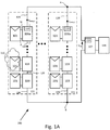
- System power device 107 may be a power converter (e.g., a direct current (DC) to alternating current (AC) inverter), a combiner box, and/or a monitoring, control and communications device.
- Load 109 may be a utility grid or other load (e.g., an AC motor).
- Multiple wiring configurations 111 are shown connected in parallel at terminals A and B that connect to the input of system power device 107 and provide voltage input V AB to the input of system power device 107 .
- the output of system power device 107 may connect to load 109.
- Each wiring configuration 111 may include one or more power sources 101 that may be connected to a respective power device 103 and/or power device 103a at terminals W , X .
- the outputs of power devices 103/103a at terminals Y , Z may be connected together to form a serial string that connects between terminals A and B .
- Communication devices 110 are shown connected to system power device 107 and may also be connected to power device 103a .
- Communication device 110 may be an integrated part of system power devices 107 /power devices 103 and/or retrofit to system power devices 107 /power devices 103 . Features of communication device 110 are described in greater detail below in the descriptions that follow.
- one or more wiring configurations 111 might not include power devices 103a or 103 .
- a wiring configuration 111 may include multiple power sources 101 directly connected in series or in parallel.
- a wiring configuration 111 may have ten, twenty or thirty serially-connected photovoltaic panels.
- a wiring configuration 111 may include a first group of one or more directly connected power sources 101 , with a second group of one or more power sources 101 connected via power devices 103a or 103 connected to the first group.
- This arrangement may be useful in power installations where some power sources 101 may be susceptible to factors that reduce power generation (e.g., PV generators that are occasionally shaded by shade 112 , wind turbines that occasionally suffer from a reduction in wind and/or with other power sources 101 less susceptible to power-reducing factors.
- PV generators that are occasionally shaded by shade 112
- wind turbines that occasionally suffer from a reduction in wind and/or with other power sources 101 less susceptible to power-reducing factors.
- each power source 101 may be connected to a power device 103a having a communication device 110 .
- a single power source 101 in each wiring configuration 111 is connected to a power device 103a , and other power sources 101 in the wiring configuration are connected to a power device 103 that might not include communication device 110 .
- Providing each power device with a communication device may increase the control and communication capabilities of power system 180 (e.g., by enabling reception of commands and/or transmission of command and measurements by each power device 103 ), but may increase system cost.
- aspects of the disclosure herein are applicable to systems having communication capabilities at each power device, and also systems having a single communication device in each wiring configuration 111 .
- a communication device 110 may be located near to terminal B that may be grounded, so that from a signal perspective, both transmission and reception of signals may be with respect to a ground.
- FIG. 1B illustrates a power system 181 and details of wiring configurations 115 and corresponding connections to system power device 107 , according to illustrative aspects of the disclosure.
- System power device 107 may be the same as system power device 107 of Fig. 1A .
- Wiring configurations 115 comprise multiple serially-connected photovoltaic power devices 103a , each power device 103a receiving input power from a connected power source 101 , and each power device 103a comprising a communication device 110 .
- Each of communication devices 110 may be configured to communicate with one another and/or with system power device 107 by transmitting and/or receiving signals over power lines 120 .
- any number of communication devices 110 may be located at various locations of power systems 180/181, for example on the outputs of power sources 101 and/or load 109 .
- Fig. 1C illustrates circuitry that may be found in a power device such as power devices 103/103a, according to illustrative aspects of the disclosure.
- Power device 103/103a may be similar to or the same as power devices 103/103a shown in Fig. 1A that may provide respective input and output terminals W , X and Y , Z .
- Input terminals W , X and output terminals Y , Z may provide connection to power lines 120 (not shown).
- power devices 103/103a may include power circuit 135 .
- Power circuit 135 may include a direct current-direct current (DC/DC) converter such as a Buck, Boost, Buck/Boost, Buck+Boost, Boost + Buck, Cuk, Flyback and/or forward converter, or a charge pump.
- DC/DC direct current-direct current
- power circuit 135 may include a direct current to alternating current (DC/AC) converter (also known as an inverter), such as a micro-inverter.
- DC/AC direct current to alternating current
- Power circuit 135 may have two input terminals and two output terminals, that may be the same as the input terminals and output terminals of power device 103/103a .
- power device 103/103a may include Maximum Power Point Tracking (MPPT) circuit 138 , configured to extract increased power from a power source.
- MPPT Maximum Power Point Tracking
- power circuit 135 may include MPPT functionality.
- MPPT circuit 138 may implement impedance matching algorithms to extract increased power from a power source.
- the power device may be connected to power device 103/103a and may further include controller 105 such as a microprocessor, Digital Signal Processor (DSP), Application-Specific Integrated Circuit (ASIC), and/or a Field Programmable Gate Array (FPGA).
- controller 105 such as a microprocessor, Digital Signal Processor (DSP), Application-Specific Integrated Circuit (ASIC), and/or a Field Programmable Gate Array (FPGA).
- DSP Digital Signal Processor
- ASIC Application-Specific Integrated Circuit
- FPGA Field Programmable Gate Array
- controller 105 may control and/or communicate with other elements of power devices 103/103a over common bus 190 .
- power devices 103/103a may include circuitry and/or sensors/sensor interfaces 125 .
- Power devices 103/103a and/or sensors/sensor interfaces 125 may be configured to measure operating power parameters directly or receive measured operating power parameters from connected sensors and/or sensor interfaces 125.
- Sensors and/or sensor interfaces 125 may be configured to measure operating power parameters on or near the power source, such as the voltage and/or current output by the power source and/or the power output by the power source.
- the power source may be a photovoltaic (PV) generator comprising PV cells, and a sensor or sensor interface may directly measure or receive measurements of the irradiance received by the PV cells, and/or the temperature on or near the PV generator.
- PV photovoltaic
- power devices 103/103a may include communication interface 129 , configured to transmit and/or receive data and/or commands from other devices.
- Communication interface 129 may communicate using Power Line Communication (PLC) technology, acoustic communications technology, or additional technologies such as ZIGBEETM, Wi-Fi, BLUETOOTFITM, cellular communication, or other wireless methods.
- Power Line Communication (PLC) may be performed over power lines 120 between power devices 103/103a and system power device (e.g., inverter) 107 that may include a similar communication interface as communication interface 129 .
- Communication interface 129 may be the same as or used as communication device 110 of Fig. 1A .
- power device 103/103a may include memory device 123 , for logging measurements taken by sensor(s)/sensor interfaces 125 to store code, operational protocols or other operating information.
- Memory device 123 may be flash memory, Electrically Erasable Programmable Read-Only Memory (EEPROM), Random Access Memory (RAM), Solid State Devices (SSD), or other types of appropriate memory devices.
- EEPROM Electrically Erasable Programmable Read-Only Memory
- RAM Random Access Memory
- SSD Solid State Devices
- power device 103/103a may include safety device(s) 160 (e.g., fuse(s), circuit breaker(s) and Residual Current Detector(s)).
- Safety devices 160 may be passive or active.
- safety devices 160 may include one or more passive fuses disposed within power devices 103/103a .
- the elements of the fuses may be designed to melt and disintegrate when excess current above the rating of the fuses flows through them. The melting of the fuses thereby disconnects parts of power devices 103/103a from terminals Y , Z , W and X so as to avoid damage to power device 103/103a and other components of power systems 180/181.
- safety devices 160 may include active disconnect switches, configured to receive commands from a controller (e.g., controller 105 , or an external controller) to short-circuit and/or disconnect portions of power devices 103/103a, or configured to short-circuit and/or disconnect portions of power devices 103/103a in response to a measurement measured by a sensor (e.g., a measurement measured or obtained by sensors/sensor interfaces 125 ).
- power devices 103/103a may include auxiliary power circuit 162 , configured to receive power (from a power source connected to power devices 103/103a , and to output power suitable for operating other circuitry components (e.g., controller 105 , communication interface 129 , etc.).
- auxiliary power circuit 162 may be connected to an output of a power devices 103/103a and designed to receive power from power sources connected to other power devices.
- Power device 103/103a may include or be operatively attached to a maximum power point tracking (MPPT) circuit 138 .
- the MPPT circuit may also be operatively connected to controller 105 or another controller 105 included in power device 103/103a that may be designated as a primary controller.
- a primary controller in power device 103/103a may communicatively control one or more other power devices 103/103a that may include controllers known as secondary controllers. Once a primary/secondary relationship may be established, a direction of control may be from the primary controller to the secondary controllers.
- the MPPT circuit under control of a primary and/or central controller 105 may be utilized to increase power extraction from power sources 101 and/or to control voltage and/or current supplied to system power device (e.g., an inverter or a load) 107 .
- system power device e.g., an inverter or a load
- power device 103/103a may include bypass unit Q9 coupled between the inputs of power circuit 135 and/or between the outputs of power circuit 135 .
- Bypass unit Q9 and/or power circuit 135 may be integrated in a combiner box to terminate power lines 120 or to provide one or more safety devices such as fuses or residual current devices.
- Bypass unit Q9 may also be an isolation switch.
- Bypass unit Q9 may be a passive device (for example, a diode). Where bypass unit Q9 is an active device, bypass unit Q9 may be controlled by controller 105 . If an unsafe condition is detected, controller 105 may set bypass unit Q9 to ON, short-circuiting the input and/or output of power circuit 135 .
- each PV generator provides an open-circuit voltage at its output terminals.
- a PV generator When bypass unit Q9 is ON, a PV generator may be short-circuited, to provide a voltage of about zero to power circuit 135 .
- a safe voltage may be maintained, and the two scenarios may be staggered to alternate between open-circuiting and short-circuiting PV generators. This mode of operation may allow continuous power supply to system control devices, as well as provide backup mechanisms for maintaining a safe voltage (i.e., operation of bypass unit Q9 may allow continued safe operating conditions).
- a power device 103/103a may comprise a partial group of the elements illustrated in Fig. 1B .
- a power device 103/103a might not include power circuit 135 (i.e., power circuit 135 may be replaced by a short circuit, and a single bypass unit Q9 may be featured.
- power device 103/103a may be still used to provide safety, monitoring and/or bypass features.
- bypass unit Q9 when a bypass unit Q9 is activated, a voltage drop of several 10s or 100s of millivolts may develop across bypass unit Q9 .
- the voltage drop across bypass unit Q9 may be used as auxiliary power for continued activation of bypass unit Q9 and/or operation of an adjustable impedance circuit, as disclosed in further detail below.
- a transceiver 20 may connect between terminals Y and Z between two power devices 103/103a via a coupling capacitor Cp .
- Terminals Z and Y may be included in power line 120 and/or be provided on the outputs of power device 103/103a to provide a series connection of power device 103/103a outputs.
- the series connection provides the flow of string current ( I string ) between terminals A and B through power line 120 .
- Terminal Y may connect to terminal A if communication device 110 is located and connected at power device 103a as shown in Figs. 1A and 1E .
- the total impedance (Z T ) across terminals Z and Y is the sum of an impedance Z1 of a first circuit and an impedance Z2 from a second circuit.
- Two impedance circuits Z1 and Z2 are shown as an illustrative example, additional aspects of the disclosure herein may feature more than two impedance circuits.
- One or more impedance circuits e.g., Z1
- One or more impedance circuits (e.g., Z2 ) may be passive impedance circuits designed to provide impedance values at various frequencies without need for auxiliary operating power for adjusting impedance values.
- Fig. 1E shows details of communication device 110a that may be utilized for power line communications (PLC), according to illustrative aspects of the disclosure.
- PLC power line communications
- the outputs of power devices 103/103a at terminals Y , Z may be connected together to form a serial string that connects between terminals A and B .
- One or more communication devices 110 may be coupled (e.g., directly connected) in a series connection in the serial string at any point in the serial string between terminals A and B .
- Communication device 110a of Fig. IE may be used as communication device 110 of Fig. 1A and other figures which follow.
- the communication device 110a in Fig. 1E may connect between terminal A and terminal Y of power devices 103/103a .
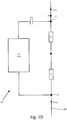
- Communication device 110a may comprise a coupling circuit that includes a first circuit 21 of inductor L1 , resistor R1 and capacitor C1 for impedance Z1 .
- the first circuit 21 may be serially connected with a second circuit 22 of inductor L2 , resistor R2 and capacitor C2 , whereby the second circuit 22 is an element of the coupling circuit.
- Inductor L2 , resistor R2 and capacitor C2 may be connected in parallel.
- the second circuit 22 may, according to some aspects, just include one of inductor L2 and/or capacitor C2 for impedance Z2 .
- a transceiver 20 may connect between terminals Z and Y between two power devices 103/103a via a coupling capacitor Cp .
- Capacitor C1 may be adjustable to provide a variable capacitance value responsive system conditions to enable increased transmission efficiency of a signal onto a power line 120 .
- Transmission efficiency may be defined as the ratio of the power received by a communication device 110a over a transmission path (e.g., powerlines 120 ) to the power transmitted by another communication device 110 .
- Capacitor C1 may be implemented as an active capacitor circuit, a bank of switched capacitors or by use of a tuning diode, also known as a varactor diode, variable capacitance diode, varicap diode or variable reactance diode.
- Tuning diodes may have a variable capacitance that is a function of the voltage that is impressed on their terminals.
- Fig. IF shows more details of communication device 110b that may be utilized for power line communications (PLC), according to illustrative aspects of the disclosure.
- Communication device 110b in Figure ID is the same as in Fig. 1C except that capacitor C3 may replace variable capacitor C1 , and inductor L1 may be replaced by inductor L3 .
- Inductor L3 may be an adjustable inductor to provide a variable inductance value to enable increased transmission efficiency of a signal onto power line 120 and/or increase reception efficiency from a signal present on powerline 120 .
- Inductor L3 may be implemented as an active inductor circuit to provide a variable inductance value. Another implementation may be to use both variable inductor L3 and variable capacitor C1 in order to enable increased transmission efficiency of a signal onto power line 120 .
- Impedance Z1 may be connected in series with impedance Z2 and as mentioned previously impedance Z2 may include inductor L2 , inductor L2 and capacitor C2 in parallel. Operation of impedance Z1 may be responsive to electrical parameters of power systems 180/181 sensed by sensors 204a /sensor interfaces 125/204 for example. Operation of impedance Z1 may be responsive to further electrical parameters of sensed by sensors described above with respect to transceiver 20 to enable for example power line communications (PLC) or arc detection, for example.
- PLC power line communications
- the power to operate and control impedance Z1 may be obtained from a power source connected to a device including impedance Z1 (e.g., with respect to Fig. 1A ).
- a power source 101 may provide operational power for an impedance Z1 included in a corresponding power device 103/103a ), from the power in a respective string of serially connect power devices 103a/103 or from other points in power systems 180/181 described above.
- the power to operate impedance Z1 may also be obtained from auxiliary power circuit 162 or other sources of auxiliary power such as batteries or from a utility grid for example.
- Sensing and control of impedance Z1 may be by controller 105 or other controllers, sensors mentioned above and in further in the descriptions which follow.
- variable capacitor C1 shown in Fig. IE may be realized by a bank of switchable capacitors C .
- Each capacitor C may be selected to connect between terminals Y and Z by a number (n) of switches S1-Sn .
- Each capacitor C may have the same value or a range of different values which depending on the combination states of switches S1-Sn being either ON or OFF present a discrete range of values of capacitance. The discrete range of values of capacitance may applied and varied across terminals Y and Z .
- Switches S1-Sn may be implemented with solid state switches, such as metal oxide semiconductor field effect transistors (MOSFETs), junction field effect transistors (JFETs), insulated gate bipolar transistors (IGBTs) or bipolar junction transistors (BJTs). Switches S1-Sn may be implemented with mechanical single pole switches or electro-mechanical relays.
- MOSFETs metal oxide semiconductor field effect transistors
- JFETs junction field effect transistors
- IGBTs insulated gate bipolar transistors
- BJTs bipolar junction transistors
- Switches S1-Sn may be implemented with mechanical single pole switches or electro-mechanical relays.
- variable capacitor C1 shown in Fig. IE may be realized by a bank of 'n' varicap diodes V cap1 -V capn (also known as varactor diodes) that may exploit the voltage-dependent capacitance of their reversed-biased p-n junction. Therefore, biases applied to varicap diodes V cap1 -V capn may be used to select which varicap diode and its capacitance responsive to the bias is applied across terminals Y and Z and/or the level of string current I string .
- V cap1 -V capn also known as varactor diodes
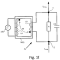
- inductor L5 may be connected in parallel with resistor R1 and capacitor C3 across terminals Y and Z .
- Capacitor C3 may be a fixed value capacitor or may be implemented as a variable capacitor as shown with respect variable capacitor C1 shown in Figs. 1G and 1H .
- Inductor L5 may be wound on a magnetic core MC1 along with inductor L4 that may also be wound on magnetic core MC1 .
- Inductors L5 and L4 have a mutual inductance ( M ) where mutual inductance ( M ) occurs when, for example, the change in current in inductor L4 induces a voltage in nearby inductor L5 and vice versa; when, for example, the change in current (significant portion of I string ) in inductor L5 induces a voltage in nearby inductor L4 .
- a configurable (e.g., adaptable) current source 165 may connect across inductor L4 . Therefore, a sensor 204 a/sensor interface 204 of transceiver 20 and/or sensors/sensor interfaces 125 may sense the level of string current I string and inject a level of current from current source 165 through inductor L4 .
- the injection of the level and direction of current from current source 165 into inductor L4 may be responsive to the sensed level of string current I string beyond which inductor L5 becomes saturated.
- the level of current from current source 165 into inductor L4 may have the effect of altering the level of flux ( ⁇ ) in magnetic core MC1 so that inductor L5 becomes less saturated.
- the current injected from current source 165 may oppose the string current I string by virtue of the mutual inductance M between inductors L4 and L5 .
- a look up table of string current I string levels may provide the appropriate level of current and direction of current to be injected into inductor L4.
- an additional inductor (not explicitly shown, for clarity) may be disposed in series with inductor L4 and/or a capacitor (not explicitly shown, for clarity) may be disposed in parallel with inductor L4 to increase the impedance reflected towards inductor L5 .
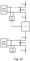
- Fig. 1J shows a diagram of how auxiliary power may be supplied to adjustable impedance circuits and/or communication devices described above, according to illustrative aspects of the disclosure.
- Fig. 1J shows a partial portion of a series string of power devices 103a/103 outputs.
- the supply auxiliary power to communication devices may be designed to receive power from power sources connected to other power devices and/or sources of power independent from power produced by power systems 180/181 as shown in Figs.1A and 1B .
- Auxiliary power circuit 262 may be connected to an output of a power device 103/103a, the output of power device 103/103a has a bypass diode BPD1 connected across terminals Y and Z of power device 103/103a .
- Device 191 In series between terminal Z of one power device 103/103a and terminal Y of another power device 103/103a is a device 191 .
- Device 191 may be, for example, a communication device 110/110a/110b/117 having an adjustable impedance circuit Z1 such as shown in Figs. 1G, 1H , and 1I .
- a reverse bias may appear across terminals Y and Z and bypass diode BPD1 is forward biased.
- the forward bias of BPD1 and current I string passing through a power device 103/103a output may be used by auxiliary power circuit 262 to provide an operating power to an associated device 191 .
- the operating power maybe utilized and be sufficient to power the operation the first circuit of a device 191 .
- an adjustable impedance circuit Z1 may be installed in a series string of power devices to increase or decrease the total impedance of the series string according to operational considerations. For example, when a transmitter in a different serial string is transmitting, it may be beneficial for impedance circuit Z1 (which may, in this case, feature only an inductor, or an inductor with an adjustable capacitor but without a resistor, or a full RLC circuit) to be operated to increase the string impedance, to prevent leakage of the signal into the serial string.
- impedance circuit Z1 which may, in this case, feature only an inductor, or an inductor with an adjustable capacitor but without a resistor, or a full RLC circuit
- device 191 may be an arc-detection circuit configured to measure voltage and/or current at a certain frequency, and based on the magnitudes of the measurements, determine whether an arc may be present in the system.
- the arc detection device may include an adjustable impedance circuit adjusted to achieve high impedance at a frequency that is reasonably "clean", i.e., a frequency not used for other purposes and not “noisy" due to external system factors.
- the adjustable impedance may be adjusted to provide high impedance for improved measurement and improved arc detection at the selected frequency.
- communication devices using wiring configurations similar to wiring configuration 111 of Fig. 1A may be required to operate under a wide range of system conditions.
- a large direct current (DC) current flows through communication device 110 (e.g., when power sources 101 of Fig. 1A are irradiated by substantial sunlight and are producing substantial power)
- an inductor with a low saturation current may become saturated and cease to operate as an effective impedance for communications.
- power sources 101 are under producing current (e.g., due to shading, or at dusk or dawn)
- an inductor having low inductance might not sustain current in a satisfactory manner.
- Using a single inductor having both high saturation current and high inductance may be expensive.
- Designing communication devices 110 and/or 110a to have a first circuit and a serially-connected second circuit may enable component selection to provide high performance under various operating conditions.
- the second circuit may include inductor L2 that may be a high-inductance inductor (e.g., having an inductance of 5 ⁇ H , 10 ⁇ H , 20 ⁇ H , etc.), but might have low saturation current.
- the first circuit may serve as a variable impedance adjustable to present an equivalent impedance according to system parameters (e.g., line inductance and impedance), and the inductor L1 of the first circuit may have a high saturation current to prevent saturation when substantial current flows through the communication device.
- the first circuit impedance may be adjusted by changing the capacitance of capacitor C1 .
- inductor L1 may be implemented as per Fig. 1I with mutual inductors L4 and L5 so that the level of current from current source 165 into inductor L4 may have the effect of altering the level of flux ( ⁇ ) in magnetic core MC1 so that inductor L5 that may have the same inductance as inductor L1 becomes less saturated.
- the first circuit may provide the features of a variable impedance ( Z ) and bandwidth ( BW ) along with the feature to extended the level to which an equivalent inductor of the first circuit is saturated responsive to the level of string current I string .
- L is inductance and C is capacitance.
- Q f r BW
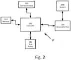
- Controller 200 may include a microprocessor, microcontroller and/or digital signal processor (DSP) that may be connected to memory device 210 .
- Memory device 210 may be similar to or the same as memory device 123 of Fig. 1C .
- controller 200 in one communication device 110 may serve as a central controller to the other controllers 200 of the other communication devices 110 . Therefore, communications interface 202 connected to controller 200 may provide communications between controllers 200 and other controllers 200/105 included in power system 180 , for example.
- the communications to and from communications interfaces 202 of communication devices 110 may be by power line communication (PLC) over power lines 120 according to the circuit features described below with respect to communication device 110.
- Communications in communications interface 202 may also include measured or sensed communication parameters via sensors 204a /sensor interface 204 .
- Communications interfaces 202 may communicate with a local area network or cellular network in order to establish an internet connection that, for example, may provide a feature of remote control, remote monitoring and/or reconfiguration of power devices 103/103a and/or system power device 107 , for example.
- Transceiver 20 may further include auxiliary power circuit 262 , configured to receive power from a power source connected to power device 103/103a, system power device 107 and output power suitable for operating other circuitry components (e.g., controller 200 , communication interface 202 , etc.).
- auxiliary power circuit 262 may be connected to an output of a power device 103/103a, system power device 107 and designed to receive power from power sources connected to other power devices and/or sources of power independent from power produced by power system 180 .
- FIG. 3A which shows illustrative impedance curves of the first impedance circuit first impedance circuit of inductor L1 , resistor R1 and adjustable capacitor C1 and the second impedance circuit of inductor L2, resistor R2 and capacitor C2 of Fig. 1C according to illustrative aspects of the disclosure.
- the vertical axis indicates impedance (
- Response curve 34 also has a resonant frequency ( f r ) of about 50.3kHz, with a Q -factor of about 31.62 and a bandwidth BW2 of about 1.59kHz.
- the second impedance circuit Z2 may include inductor L2 that may provide an inductance of 10 ⁇ H at low current (e.g., when the current flowing through impedance circuit Z2 is less than a saturation current of 1A) but may saturate at higher currents (e.g., above 1A), and therefore, impedance curve 32 may accurately depict the impedance of second impedance circuit Z2 only under low current.
- the second impedance circuit Z2 may provide an impedance close to 0 ⁇ , due to inductor L2 saturating and "shorting" the impedance circuit.
- the second impedance circuit Z2 may provide the desired impedance at low current levels.
- the first impedance circuit Z1 may provide the desired impedance by an impedance controller adjusting capacitor C1 to have a capacitance of about 10 ⁇ F .
- the combination of impedances Z1 and Z2 may perform substantially the same as a passive impedance featuring an inductor having both high inductance and a high saturation current, and at a fraction of the cost of the passive impedance circuit.
- Adjusting one or more component values of a variable impedance circuit may provide further advantage. For example, by implementing a high-Q, low-bandwidth impedance (e.g., second impedance circuit Z2 ) with a resonant frequency that is adjustable by adjusting the value of a capacitor, high impedance can be selectively obtained at various frequencies. Changing the resonant frequency of an impedance circuit may be useful, for example, for operating an impedance circuit in multiple modes of operation.
- a high-Q, low-bandwidth impedance e.g., second impedance circuit Z2
- an impedance circuit may be desirable for the impedance circuit to provide a first resonant frequency value while in a first mode of operation (e.g., Rx, or a receiving mode) and to provide a second resonant frequency value while in a second mode of operation (e.g., Tx, or a transmitting mode).
- a first mode of operation e.g., Rx, or a receiving mode
- a second resonant frequency value while in a second mode of operation
- Figs. 3B and 3C show illustrative impedance curves 30 of the first impedance circuit of inductor L1 , resistor R1 and adjustable capacitor C1 and the second impedance circuit of inductor L2 , resistor R2 and capacitor C2 of Fig. 1C , according to illustrative aspects of the disclosure.
- Fig. 3C shows a "zoomed-in" view of a portion of Fig. 3B .
- Response curve 32 may have a low Q factor (about 3.16) and wider bandwidth BW2 (about 15.9 kHz) compared to response curves 34a and 34b which may have higher Q factors (about 33.2 and 33.0, respectively) and narrower bandwidths (about 1.45 kHz and about 1.77 kHz, respectively) compared to impedance curve 32 since with respect to Table 1 (shown below) capacitor C1 has about ten times more capacitance (e.g., nine times more or eleven times more capacitance) than capacitor C2 and/or inductor L3 (of Fig. 1D ) has ten times less inductance than inductor L2 .
- Capacitor C1 may be adjusted such that first impedance circuit Z1 selectively provides a high impedance (in this numerical example, 10 ⁇ ) at different frequencies.
- impedance circuit Z1 When operational power is not available for adjustment of capacitor C1 (e.g., when a power source connected to impedance circuits Z1 and Z2 is not producing substantial power, indicating a low-current flow through impedance circuits Z1 and Z2 ), impedance circuit Z1 may be unsaturated and may provide a high impedance across a reasonably broad bandwidth (in this example, about 15.9 kHz).
- Capacitor C1 may be adjusted to be 9 ⁇ F when a PLC device is in a first (e.g., transmitting) mode, and capacitor C1 may be adjusted to be 11 ⁇ F when a PLC device is in a second (e.g., receiving) mode.
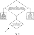
- FIG. 4A shows a flow chart of a method 400 , according to illustrative aspects of the disclosure.
- Power systems 180/181 includes multiple strings of wiring configurations 111/115 that are connected in parallel at terminals A and B .
- Wiring configurations 111/115 may include power converter 103/103a whose outputs are connected in series to form the multiple strings of wiring configurations 111/115 connected in parallel at terminals A and B and whose inputs are connected to power sources 101 .
- Power converters 103/103a may be DC to DC converters and power sources 101 may be photovoltaic panels, for example.
- Wiring configurations 111/115 and their interconnections, monitoring and control are designed to achieve an efficient power delivery to load 109 . Therefore, the efficient power delivery may be by reliable communication signals conveying control signals and monitoring signals between components of power systems 180/181 .
- reliable communications may be carried out between components of power systems 180/181 and may enable proper efficient operation of power system 180 . Therefore, efficient transmission and reception of communication signals by power line communications may consider the control of adjustments of communication parameters of the communication coupling circuits of communication devices 110 , as well as the passive communication parameters of the communication coupling circuits of communication devices 110 . Consequently, the use of passive communication parameters and/or adjustments of communication parameters may convey communication signals responsively to the operating power parameters of power system 180 .
- Operating power parameters of power system 180 may include MPPT circuitry to extract increased power from a power source 101 and/or levels of V AB or string currents I string 1 , I string 2 to be applied efficiently to load 109 via system power device 107 that also may include MPPT circuitry.
- communication device 110 may connect in a series connection in the serial string at any point in the serial string between terminals A and B as shown in Fig. 1A .
- the series connection in Fig. 1B may connect between terminal A and terminal Y of power devices 103/103a .
- the series connection may include a first circuit of inductor L1 , resistor R1 and capacitor C1 .
- the first circuit may be serially connected with a second circuit of inductor L2 , resistor R2 and capacitor C2 .
- the first and the second circuit may include respective resistors R1 and R2 .
- the second circuit may include inductor L2 and/or capacitor C2 .
- DC power to the input of power device 107 may be via string currents I string 1 and I string 2 , conveyed by power lines 120 . Therefore, DC power to the input of power device 107 is not impeded by the first and the second circuits since the flow of string currents I string 1 , I string 2 is through inductors L1 and L2 .
- the flow of string currents I string 1 , I string may be reduced.
- Reduced flow of string currents I string 1 , I string 2 may be because power sources 101 are occasionally shaded by shade 112 , there is a faulty power device 103/103a that needs to be bypassed by bypass unit Q9 , and/or when power system 180 is operating at dawn or dusk, for example.
- a resonant frequency ( f r ) of 50.3 KiloHertz (KHz) is chosen for power line communications and nearest preferred values for inductor ( L ) and capacitor ( C ) in the first row of Table 1 that shows how the impedance ( Z ) varies for frequencies ⁇ of the resonant frequency ( f r ) .
- Quality factor of 2.35 and bandwidth ( BW ) of 26 KHz are derived from respective equations Eq. 5 and Eq. 6.
- Narrow band power line communication PLC may operate from 3 KHz to about 500 KHz.
- Band A is between 3 - 95 KHz for Utilities / smart grids
- Band B is between 95 - 125 KHz and is unrestricted
- Band C is between 125 - 140 KHz for home networks
- Band D is between 140 - 148.5 KHz for alarms and security systems.
- the second row of Table 1 shows how the impedance ( Z ) varies for frequencies ⁇ of the resonant frequency ( f r ) for L ⁇ 10 and C ⁇ 10 so that both possibilities for the selection of inductor ( L ) and capacitor ( C ) shown in the two rows have the same resonant frequency ( f r ) of 61.03 KHz.
- Quality factor ( Q ) of 23.5 and bandwidth ( BW ) of 26 KHz are derived from respective equations Eq. 5 and Eq. 6.
- Inductors L1 and L2 may be formed/ wound on ferrite cores or toroidal cores.
- the first circuit of inductor L1 , resistor R1 and capacitor C1 may have an inductor for L1 that corresponds with the second row of Table 1 so that there is a lower inductance value, and higher Q value, but the ferrite core that inductor L1 is wound on has a higher saturation current compared to the choice of inductor L2 .
- Inductor L2 used in the second circuit that corresponds with the first row of Table 1 has a higher inductance value, and lower Q value, but the ferrite core that inductor L2 is wound on has a lower saturation current compared to the choice of inductor L1 .
- power line communications under 'higher' normal levels of string currents I string 1 , I string 2 may use the first circuit of inductor L1 , resistor R1 and an adjustable capacitor C1 when operating power for transceiver 20 is derived from power generated by power system 180 .
- Power line communications under 'lower' levels of string currents I string 1 , I string 2 when a power source 101 is shaded, for example, or it is dusk or dawn, may derive benefits from circuit performance of the second circuit of inductor L2 , resistor R2 and capacitor C2 when operating power for transceiver 20 may be derived from an auxiliary power such as power from auxiliary power circuits 162/262 , the auxiliary power being independent of power generated by power system 180.
- transceiver 20 may connect between terminals Z and Y between two power devices 103/103a via a coupling capacitor Cp .
- modulation schemes can be used for power line communications.
- Some modulation schemes may include Orthogonal Frequency Division Multiplexing (OFDM), Binary Phase Shift Keying (BPSK), Frequency Shift Keying (FSK), or Spread-FSK (S-FSK).
- OFDM in particular may offer high data rates, but may require more computational power to produce Fast Fourier Transforms (FFT) and Inverse-FFT (IFFT), as required by the scheme.
- FFT Fast Fourier Transforms
- IFFT Inverse-FFT
- BPSK, FSK are robust and simple but offer lower data rates.
- power line communication for power systems like power system 180 may utilize simplex, half duplex, and/or full duplex.
- simplex communication power lines 120 a channel is formed that may be operated in one direction at a time, whereas in half duplex each communication devices 110 can communicate with the other but not simultaneously unlike full duplex.
- communication parameters of each communication devices 110 may be sensed by sensors 204a to provide the resonances of the first and second circuits, the Q factor of the resonances, the bandwidth ( BW ) of the first and second circuits, the resistances of the first and second resistors or the impedances of the first and second circuits.
- Sensing at step 405 may also include transmission of a test pulse and the communication parameters sensed may include a measure of the voltage standing wave ratio (VSWR) of the test pulse. Therefore, alteration of the first parallel circuit and/or adjustment of an additional matching network (not shown) connected at terminals A and Y may be made to try ensure an improved signal transmission of a transmitted signal from transceiver 20.
- VSWR voltage standing wave ratio
- Step 405 may also allow sensors 204a to sense an operating power parameter such as string currents I string 1 , I string 2 or voltages in a string or the voltage V AB and/or current at terminals A and B for example.
- an operating power parameter such as string currents I string 1 , I string 2 or voltages in a string or the voltage V AB and/or current at terminals A and B for example.
- Step 405 may also include the operating power parameters to be sensed by sensors/sensor interfaces 125 of power devices 103/103a and/or system power devices 107 .
- Sensors 204a may also be configured to measure operating power parameters directly or receive measured operating power parameters from other connected sensors and/or sensor interfaces 125/204a that may be a part of power devices 103/103a and/or system power devices 107 . Therefore, operating power parameters may be sensed and/or measured on or near the inputs and outputs of power sources 101 , power devices 103/103a and/or system power devices 107 . Operating power parameters may be sensed and/or measured such as the voltage and/or current output by power source 101 and/or the power output by power source 101 for example.
- power source 101 may be a photovoltaic (PV) generator comprising PV cells
- sensor or sensor interface 125/204a may directly measure or receive measurements of the irradiance received by the PV cells, and/or the temperature on or near the PV generator, for example.
- PV photovoltaic
- a spectrum of signals may be used for power line communication within a certain bandwidth ( BW signals ) that may be centered around the center frequency ( f c ).
- the center frequency ( f c ) may be the same as the resonant frequency ( f r 2 ) of the second circuit and/or may be the same as the resonant frequency ( f r 1 ) of the first circuit.
- the resonant frequency ( f r 1 ) of the first circuit may be selected by adaptive control and/or by robust control by virtue of capacitor C1 and/or inductor L1 being adjustable, sensing and control as part of step 405 may ensure that a transmission of a signal from a transceiver 20 is to be received by other transceivers 20 using a high Q as shown by impedance curve 34 .
- the high Q may allow for a higher signal to noise ratio in the channels provided by power lines 120 to enable efficient power line communications between communication devices 110 .
- a scenario may exist where a transmission by a transceiver 20 may be absorbed and attenuated by another receiving transceiver 20 where its first circuit is outside bandwidth BW1 of impedance curve 34 .
- bandwidth BW1 of impedance curve 34 may be by virtue of insufficient power to provide adjustable control of its first circuit responsive to sensing at step 405 .
- the impedance ( Z T ) of the receiving transceiver 20 is lower when outside bandwidth BW1 of impedance curve 34 compared to the impedance ( Z T ) at resonance f r 2 for a second parallel circuit. From a signal perspective, transmission by a transceiver 20 may be absorbed and attenuated by another receiving transceiver 20 operating outside bandwidth BW1 of impedance curve 34 .
- a feature and benefit of including the second circuit in series with the first circuit may be to ensure reception of transmitted signals because of the wider bandwidth BW2 provided by the second circuit and/or with reference to equations Eq.10 and Eq.11, a higher impedance ( Z T ) may be provided that may prevent absorption and attenuation by another receiving transceiver 20 .
- communication signals may be transmitted and/or received responsive the communication parameters and/or operating power parameters sensed at step 405 , according to the variety of modulation schemes included in the description of step 403 .
- Fig. 4B shows more details of step 407 , according to illustrative aspects of the disclosure.
- simplex communication over power lines 120 to form a channel that may be operated in one direction at a time Therefore, one transceiver 20 in a transmit mode is described and one or more transceivers 20 are used in a receive mode to receive transmissions from the one transceiver 20 in the transmit mode.
- an indication for a control algorithm running on a controller 200 used as a central controller may give an indication that; 1.) all strings are operating at normal levels of current; 2.) a minority of strings are operating at low levels of current; and 3. a majority of strings are operating at low levels of current.
- step 422 all strings of serially connected outputs of power devices 103/103a between terminals A and B are operating at normal levels of current.
- Power devices 103/103a operating at normal levels of current being indicative of power sources 101 (PV generators) are fully illuminated and fully operational. Therefore, power from power system 180 may be used to provide operating power to transceivers 20 to enable transceiver 20 to transmit signals onto power lines 120 with the high Q provided from the first circuit.
- the first circuit controlled by controller 200 from communication parameters sensed by sensors 204a at step 405 may allow the resonant frequency ( f r 1 ) to be selected by adaptive control and/or by robust control by virtue of capacitor C1 and/or inductor L1 being adjustable.
- the resonant frequency ( f r 1 ) selected by adaptive control and/or by robust control at step 422 similarly applies to power from power system 180 used to provide operating power to transceivers 20 to enable transceivers 20 to receive signals from power lines 120 with the high Q provided from the first circuit.
- a majority of strings of serially connected outputs of power devices 103/103a between terminals A and B may be operating at low levels of current.
- Power devices 103/103a operating at low levels of current may be indicative of power sources 101 (PV generators) operating with low levels of illumination such as at dusk or dawn for example. Therefore, an auxiliary power from auxiliary power circuits 162/262 may be needed to provide operating power to transceivers 20 to enable transceiver 20 to transmit signals onto power lines 120 with the low Q provided from the second circuit.
- the auxiliary source of power may be independent from the source of power from power system 180 .
- resonant frequency ( f r 1 ) may not allow the resonant frequency ( f r 1 ) to be selected by adaptive control and/or by robust control of capacitor C1 and/or inductor L1 being adjustable.
- the resonant frequency ( f r 2 ) of the second circuit has a lower Q but wider band width ( BW2 ) as shown by impedance curve 32 in Fig. 3A .
- auxiliary power from auxiliary power circuits 162/262 may be needed to enable transceivers 20 to receive signals from power lines 120 with the low Q provided from the second circuit.
- the higher inductance value of L2 compared to inductor L1 means at the low-level currents, saturation of L2 is not an issue so that L2 may be at least made to the same standard as inductor L1 that has a lower inductance value.
- a minority of strings of serially connected outputs of power devices 103/103a between terminals A and B may be operating at low levels of current (e.g., 0A or close to 0A), whereas other serially connected outputs of power devices 103/103a are operating at normal levels.
- Power devices 103/103a operating at low levels of current may be indicative of power sources 101 (PV generators) operating with low levels of illumination because of shading of power sources, or indicative that a power device 103/103a is faulty.
- the faulty power devices and/or shaded power sources 101 (PV generators) may be bypassed using bypass unit Q9 as shown in Fig. 1B , in order to increase the string current.
- an auxiliary power from auxiliary power circuits 162/262 may be needed to provide an operating power to transceivers 20 .
- the operating power may enable transceiver 20 to transmit signals onto power lines 120 and/or receive signals from power lines 120 with the low Q provided from the second circuit. If as a result of the application of bypass unit Q9 , the string currents are within an acceptable range, power from power system 180 may be used to provide an operating power to transceivers 20 .
- the operating power may enable transceiver 20 to transmit signals onto power lines 120 and/or receive signals from power lines 120 with the high Q provided from the first circuit that may have the property of being adjustable.
- Method 430 may be carried out by a controller of a communication device such as communication device 110 of Figs. 1A , 1B , communication device 117 of Fig. ID, or communication device 110a of Fig. IE.
- a controller of a communication device such as communication device 110 of Figs. 1A , 1B , communication device 117 of Fig. ID, or communication device 110a of Fig. IE.
- communication device 110a of Fig. IE having variable capacitor C1 .
- Communication device 110a may generally be in a receiving mode for a majority of the system operation time, and may be a transmitting mode for a short period of time (e.g., tens or hundreds of milliseconds) periodically.
- Communication device 110a may have a first preferred impedance level while in receiving mode, and may have a second preferred impedance level while in transmitting mode.
- a controller implementing method 430 may determine if it is desirable to transmit a signal (e.g., if a substantial period of time has elapsed since the last transmission). The determination may include receiving a clock measurement and/or calculating a period of time elapsed since a prior transmission. If the controller determines that it is not time to transmit a signal, the controller may proceed to step 438 , wait a period of time (e.g., several seconds), and return to step 432 .
- a period of time e.g., several seconds
- the controller may proceed to step 434 and may adjust an impedance of communication device 110a to be at a preferred impedance level for transmitting. For example, capacitor C1 may be adjusted to present a different impedance level.
- communication device 110a may transmit a signal (e.g., over power lines 120 ).
- the controller may re-adjust the impedance to be at a level preferred for receiving mode, and may then return to step 432.
- the ability to easily shift f r having a substantial Q-factor from around 50 KHz to around 70 KHz may increase the quality of communication carried out over power lines.
- While not transmitting, communication devices may be operated to present a reduced impedance to other, transmitting, communication devices, reducing the total loop impedance "seen" by the transmitting communication device.
- the second circuit of communication device 110a having inductor L2 , resistor R2 and capacitor C2 may present a constant impedance having a higher bandwidth and lower gain compared to the first, variable circuit having inductor L1 , resistor R1 and capacitor C1 .
- the second circuit may provide adequate impedance in a case where the first circuit is inoperable, which may be due to lack of availability of power for varying capacitor C1 .
- Varying capacitor C1 may be implemented as a bank of parallel-connected capacitors that may be connected and disconnected from each other via switches as shown in Fig. 1G that may be switched responsive to step 432 .
- Method 440 may be carried out by a controller of a communication device such as communication device 110 of Figs. 1A , 1B or communication device 110a of Fig. IE.
- a controller of a communication device such as communication device 110 of Figs. 1A , 1B or communication device 110a of Fig. IE.
- communication device 110a of Fig. IE having variable capacitor C1 .
- the controller controlling capacitor C1 e.g., by opening and closing switches S1..Sn of Fig. 1G
- the communication device including the controller may be transmitting.
- a communication device that is part of the same serial string as the instant controller carrying out method 440 may be transmitting.
- a communication device that is not part of the same serial string as the controller carrying out method 440 may be transmitting.
- the controller may receive and decode a message (e.g., sent by system power device 107 of Fig. 1A ) indicating that a communication device is scheduled to transmit a communication.
- a message e.g., sent by system power device 107 of Fig. 1A
- step 442 might not be featured, and the controller may operate according to a predetermined time schedule indicating when various communication devices should transmit.
- the controller determines which communication device is scheduled to transmit, according to the message received at step 442 and/or according to the predetermined time schedule.
- the controller may proceed to step 450 and adjust (e.g., increase, or move the resonant frequency of) the impedance of an adjustable impedance circuit included in the communication device to be suitable for a transmitting mode. For example, if a message is to be transmitted at a frequency of 53 kHz, the controller may adjust capacitor C1 to be 9 ⁇ F and obtain an impedance curve similar to curve 34b of Fig. 3C .
- the controller operates the communication device to transmit the message.
- the controller adjusts the impedance to be suitable for a receiving mode of the communication device.
- the controller may, at step 447 , adjust the impedance to provide a reduced impedance at the frequency used by the transmitting controller, to reduce in-string attenuation of the signal, or an increased impedance at the frequency used by the transmitting controller. For example, where it is desirable to receive in-string communications, the controller may increase the impedance. Where it is not desirable to receive in-string communications (e.g., where the intended recipient of the message is not in the serial string), the controller may reduce the impedance. After transmission is complete, at step 448 , the controller continues to step 449 and adjusts the impedance to be in a receiving mode of the communication device.
- the controller may, at step 444 , adjust the impedance to provide an increased impedance at the frequency used by the transmitting controller, to reduce leakage of the signal into the string.
- the controller continues to step 446 and adjusts the impedance to be in a receiving mode of the communication device.
- Wiring configuration 115a may comprise serially connected power devices 103b...103m
- wiring configuration 115b may comprise serially connected power devices 103n...103z.
- Each power device 103b...103z may be similar to power device 103a of Fig. 1B and may include a communication device 110 having an impedance Z .
- Each power device may have a controller (e.g., controller 105 of Fig. 1C ) configured to carry out method 440 of Fig. 4D .
- Fig. 4E depicts a time in which the controllers of power devices 103b...103z are carrying out method 440 . It may depict a time where the communication device of power device 103c is transmitting or preparing to transmit. Prior to the time shown in Fig. 4E , the controller of power devices 103b..103z determine (either by decoding a message or according to a predetermined schedule) that the communication device of power device 103c is to transmit. The controllers of power devices 103b and 103m control respective adjustable impedances to be at a low impedance level (in accordance with step 447 of method 440 ) as to not attenuate the transmission by power device 103c.
- the controller of power device 103c controls a corresponding adjustable impedance to be at a high impedance level (in accordance with step 450 of method 440 ) to enable an effective transmission by power device 103c, and the controllers of power devices 103n...103z control respective adjustable impedances to be at a high impedance level (in accordance with step 444 of method 440 ) as to increase the impedance of wiring configuration 115b and reduce the leakage of the transmission by power device 103c into wiring configuration 115 .
- each or either of methods 430 and 440 may be carried out by communication devices 110 of Figs. 1A or 1B .
- Impedance Z1 of Fig. ID may be realized by any of the circuits Z1 of Figs. 1E-1I .
- a circuit or system including more than one adjustable impedance may feature different types of adjustable impedances (for example, a first power device may feature impedance Z1 of Fig. 1I and a second power device may feature impedance Z1 of Fig. 1G ).
- circuits disclosed herein may include elements used according to some aspects but not according to other aspects.
- impedances Z1 and Z2 of Fig. ID may be used independently as part of power devices featuring an adjustable impedance, and transceiver 20 and capacitor Cp may be added in power devices further featuring a communication device 110.
- resistor R1 and capacitor C3 may be removed from impedance Z1 of Fig. 1I .
- the resultant impedance Z1 may be effectively that of an inductor with a compensation circuit designed to prevent the saturation of inductor L5 .
Priority Applications (1)
| Application Number | Priority Date | Filing Date | Title |
|---|---|---|---|
| EP20188664.5A EP3751746B1 (fr) | 2017-12-28 | 2018-12-19 | Circuit d'impédance variable |
Applications Claiming Priority (1)
| Application Number | Priority Date | Filing Date | Title |
|---|---|---|---|
| US201762611006P | 2017-12-28 | 2017-12-28 |
Related Child Applications (2)
| Application Number | Title | Priority Date | Filing Date |
|---|---|---|---|
| EP20188664.5A Division EP3751746B1 (fr) | 2017-12-28 | 2018-12-19 | Circuit d'impédance variable |
| EP20188664.5A Division-Into EP3751746B1 (fr) | 2017-12-28 | 2018-12-19 | Circuit d'impédance variable |
Publications (2)
| Publication Number | Publication Date |
|---|---|
| EP3506516A1 true EP3506516A1 (fr) | 2019-07-03 |
| EP3506516B1 EP3506516B1 (fr) | 2020-10-28 |
Family
ID=64746157
Family Applications (2)
| Application Number | Title | Priority Date | Filing Date |
|---|---|---|---|
| EP20188664.5A Active EP3751746B1 (fr) | 2017-12-28 | 2018-12-19 | Circuit d'impédance variable |
| EP18214027.7A Active EP3506516B1 (fr) | 2017-12-28 | 2018-12-19 | Circuit d'impédance variable |
Family Applications Before (1)
| Application Number | Title | Priority Date | Filing Date |
|---|---|---|---|
| EP20188664.5A Active EP3751746B1 (fr) | 2017-12-28 | 2018-12-19 | Circuit d'impédance variable |
Country Status (3)
| Country | Link |
|---|---|
| US (4) | US10630342B2 (fr) |
| EP (2) | EP3751746B1 (fr) |
| CN (2) | CN114337735B (fr) |
Cited By (2)
| Publication number | Priority date | Publication date | Assignee | Title |
|---|---|---|---|---|
| KR20170012409A (ko) * | 2014-05-29 | 2017-02-02 | 스카이워크스 솔루션즈, 인코포레이티드 | 광대역 멀티모드 멀티-대역 프론트 엔드 모듈에서의 결합기를 위한 적응적 부하 |
| ES2862461A1 (es) * | 2020-04-06 | 2021-10-07 | Univ Valladolid | Sistema de comunicaciones sobre cableado de corriente continua en instalaciones solares fotovoltaicas |
Families Citing this family (6)
| Publication number | Priority date | Publication date | Assignee | Title |
|---|---|---|---|---|
| US20200076199A1 (en) * | 2018-09-05 | 2020-03-05 | Pika Energy, Inc. | Two-terminal electrical protective device |
| CN110535490B (zh) * | 2019-07-19 | 2022-02-22 | 重庆源联信息科技有限公司 | 一种电力线通信中的阻抗匹配系统及方法 |
| CN110854919A (zh) * | 2019-12-13 | 2020-02-28 | 浙江佳明天和缘光伏科技有限公司 | 一种直流电流型plc光伏快速关断装置 |
| CN111817753A (zh) * | 2020-07-03 | 2020-10-23 | 青岛鼎信通讯股份有限公司 | 一种零插损的中压耦合装置 |
| EP3974848A1 (fr) * | 2020-09-24 | 2022-03-30 | ABB Schweiz AG | Dispositif de détection de défaut d'arc comportant un capteur à large bande |
| CN112994751A (zh) * | 2021-02-03 | 2021-06-18 | 青岛鼎信通讯股份有限公司 | 一种宽带耦合装置 |
Citations (1)
| Publication number | Priority date | Publication date | Assignee | Title |
|---|---|---|---|---|
| EP1850501A1 (fr) * | 2006-04-26 | 2007-10-31 | IAD Gesellschaft für Informatik, Automatisierung und Datenverarbeitung mbH | Couplage adaptatif et capacitif et procédé de transmission d'informations par un câble d'alimentation blindé d'un réseau de distribution d'énergie électrique |
Family Cites Families (17)
| Publication number | Priority date | Publication date | Assignee | Title |
|---|---|---|---|---|
| US4455674A (en) * | 1981-02-19 | 1984-06-19 | Victor Company Of Japan Limited | Amplitude-modulated signal receiver having a variable Q circuit |
| US5168282A (en) * | 1989-06-22 | 1992-12-01 | Texas Instruments Deutschland Gmbh | Antenna resonant circuit |
| CH684722A5 (de) * | 1992-05-26 | 1994-11-30 | Siemens Ag Albis | Schaltungsanordnung zur Ankopplung einer Sendeeinheit an eine Uebertragungsleitung. |
| US7522878B2 (en) * | 1999-06-21 | 2009-04-21 | Access Business Group International Llc | Adaptive inductive power supply with communication |
| US7136936B2 (en) * | 2003-10-03 | 2006-11-14 | Asoka Usa Corporation | Method and system for virtual powerline local area networks |
| US7493100B2 (en) * | 2003-10-15 | 2009-02-17 | General Electric Company | Compensating for dynamic nulls in a power line communication system |
| WO2006137607A1 (fr) * | 2005-06-22 | 2006-12-28 | Leetronix Co., Ltd. | Circuits de couplage adaptatifs utilisant des reservoirs de resonance multiple |
| SI2009807T1 (sl) * | 2007-06-26 | 2010-10-29 | Eandis | Distribucijski elektrovodni komunikacijski sistem |
| ES2769398T3 (es) * | 2010-12-22 | 2020-06-25 | St Microelectronics Srl | Circuito de acoplamiento para comunicaciones por línea eléctrica |
| US8364326B2 (en) * | 2011-02-22 | 2013-01-29 | Asoka Usa Corporation | Set of sensor units for communication enabled for streaming media delivery with monitoring and control of power usage of connected appliances |
| US8755946B2 (en) * | 2011-02-22 | 2014-06-17 | Asoka Usa Corporation | Method and apparatus for using PLC-based sensor units for communication and streaming media delivery, and for monitoring and control of power usage of connected appliances |
| US20150045977A1 (en) * | 2011-06-17 | 2015-02-12 | Mingyao XIA | Method and apparatus for using plc-based sensor units for communication and streaming media delivery, and for monitoring and control of power usage of connected appliances |
| CN102594405B (zh) * | 2012-01-12 | 2014-10-29 | 美芯集成电路(深圳)有限公司 | 一种带自校准功能的电力载波通信电路 |
| US9270249B2 (en) * | 2012-08-20 | 2016-02-23 | Htc Corporation | Tunable impedance matching circuit |
| JP5751267B2 (ja) * | 2013-02-08 | 2015-07-22 | 株式会社デンソー | 車両用電力線通信システムおよびスレーブ装置 |
| US9755670B2 (en) * | 2014-05-29 | 2017-09-05 | Skyworks Solutions, Inc. | Adaptive load for coupler in broadband multimode multiband front end module |
| TWI621319B (zh) * | 2015-09-19 | 2018-04-11 | 立錡科技股份有限公司 | 諧振式無線電源發送電路及其控制方法 |
-
2018
- 2018-12-19 EP EP20188664.5A patent/EP3751746B1/fr active Active
- 2018-12-19 US US16/225,212 patent/US10630342B2/en active Active
- 2018-12-19 EP EP18214027.7A patent/EP3506516B1/fr active Active
- 2018-12-25 CN CN202111499534.XA patent/CN114337735B/zh active Active
- 2018-12-25 CN CN201811594685.1A patent/CN110022167B/zh active Active
-
2020
- 2020-03-13 US US16/817,941 patent/US11005532B2/en active Active
-
2021
- 2021-04-14 US US17/230,087 patent/US11728845B2/en active Active
-
2023
- 2023-06-27 US US18/341,959 patent/US20240030965A1/en active Pending
Patent Citations (1)
| Publication number | Priority date | Publication date | Assignee | Title |
|---|---|---|---|---|
| EP1850501A1 (fr) * | 2006-04-26 | 2007-10-31 | IAD Gesellschaft für Informatik, Automatisierung und Datenverarbeitung mbH | Couplage adaptatif et capacitif et procédé de transmission d'informations par un câble d'alimentation blindé d'un réseau de distribution d'énergie électrique |
Cited By (2)
| Publication number | Priority date | Publication date | Assignee | Title |
|---|---|---|---|---|
| KR20170012409A (ko) * | 2014-05-29 | 2017-02-02 | 스카이워크스 솔루션즈, 인코포레이티드 | 광대역 멀티모드 멀티-대역 프론트 엔드 모듈에서의 결합기를 위한 적응적 부하 |
| ES2862461A1 (es) * | 2020-04-06 | 2021-10-07 | Univ Valladolid | Sistema de comunicaciones sobre cableado de corriente continua en instalaciones solares fotovoltaicas |
Also Published As
| Publication number | Publication date |
|---|---|
| US20190207653A1 (en) | 2019-07-04 |
| CN110022167A (zh) | 2019-07-16 |
| US11005532B2 (en) | 2021-05-11 |
| CN114337735A (zh) | 2022-04-12 |
| EP3751746B1 (fr) | 2024-02-14 |
| CN110022167B (zh) | 2021-12-28 |
| US20200274578A1 (en) | 2020-08-27 |
| US10630342B2 (en) | 2020-04-21 |
| US11728845B2 (en) | 2023-08-15 |
| EP3506516B1 (fr) | 2020-10-28 |
| EP3751746A1 (fr) | 2020-12-16 |
| CN114337735B (zh) | 2024-03-08 |
| US20240030965A1 (en) | 2024-01-25 |
| US20210359720A1 (en) | 2021-11-18 |
Similar Documents
| Publication | Publication Date | Title |
|---|---|---|
| EP3506516B1 (fr) | Circuit d'impédance variable | |
| US11909205B2 (en) | Method and apparatus for high efficiency rectification for various loads | |
| US20200235654A1 (en) | Systems and Methods for Increasing Output Current Quality, Output Power, and Reliability of Grid-Interactive Inverters | |
| EP1668756B1 (fr) | Impedances actives serielles flottantes reparties pour systemes de transport d'electricite | |
| AU2019224916A1 (en) | Inductive power transfer device, especially for vehicle | |
| US20180269726A1 (en) | Inductive Power Transmitter | |
| CN113507299B (zh) | 断路器装置及配电台区通信系统 | |
| KR20200060884A (ko) | 무선 전력 송신 방법 및 장치 | |
| Katsuki et al. | A reliable electronic choke with no need of gain adjustment for wire communication system |
Legal Events
| Date | Code | Title | Description |
|---|---|---|---|
| PUAI | Public reference made under article 153(3) epc to a published international application that has entered the european phase |
Free format text: ORIGINAL CODE: 0009012 |
|
| STAA | Information on the status of an ep patent application or granted ep patent |
Free format text: STATUS: THE APPLICATION HAS BEEN PUBLISHED |
|
| AK | Designated contracting states |
Kind code of ref document: A1 Designated state(s): AL AT BE BG CH CY CZ DE DK EE ES FI FR GB GR HR HU IE IS IT LI LT LU LV MC MK MT NL NO PL PT RO RS SE SI SK SM TR |
|
| AX | Request for extension of the european patent |
Extension state: BA ME |
|
| STAA | Information on the status of an ep patent application or granted ep patent |
Free format text: STATUS: REQUEST FOR EXAMINATION WAS MADE |
|
| 17P | Request for examination filed |
Effective date: 20200102 |
|
| RBV | Designated contracting states (corrected) |
Designated state(s): AL AT BE BG CH CY CZ DE DK EE ES FI FR GB GR HR HU IE IS IT LI LT LU LV MC MK MT NL NO PL PT RO RS SE SI SK SM TR |
|
| GRAP | Despatch of communication of intention to grant a patent |
Free format text: ORIGINAL CODE: EPIDOSNIGR1 |
|
| STAA | Information on the status of an ep patent application or granted ep patent |
Free format text: STATUS: GRANT OF PATENT IS INTENDED |
|
| INTG | Intention to grant announced |
Effective date: 20200326 |
|
| GRAJ | Information related to disapproval of communication of intention to grant by the applicant or resumption of examination proceedings by the epo deleted |
Free format text: ORIGINAL CODE: EPIDOSDIGR1 |
|
| GRAP | Despatch of communication of intention to grant a patent |
Free format text: ORIGINAL CODE: EPIDOSNIGR1 |
|
| GRAS | Grant fee paid |
Free format text: ORIGINAL CODE: EPIDOSNIGR3 |
|
| GRAA | (expected) grant |
Free format text: ORIGINAL CODE: 0009210 |
|
| STAA | Information on the status of an ep patent application or granted ep patent |
Free format text: STATUS: THE PATENT HAS BEEN GRANTED |
|
| INTG | Intention to grant announced |
Effective date: 20200910 |
|
| AK | Designated contracting states |
Kind code of ref document: B1 Designated state(s): AL AT BE BG CH CY CZ DE DK EE ES FI FR GB GR HR HU IE IS IT LI LT LU LV MC MK MT NL NO PL PT RO RS SE SI SK SM TR |
|
| REG | Reference to a national code |
Ref country code: GB Ref legal event code: FG4D |
|
| REG | Reference to a national code |
Ref country code: CH Ref legal event code: EP |
|
| REG | Reference to a national code |
Ref country code: AT Ref legal event code: REF Ref document number: 1329278 Country of ref document: AT Kind code of ref document: T Effective date: 20201115 |
|
| REG | Reference to a national code |
Ref country code: DE Ref legal event code: R096 Ref document number: 602018009142 Country of ref document: DE |
|
| REG | Reference to a national code |
Ref country code: IE Ref legal event code: FG4D |
|
| REG | Reference to a national code |
Ref country code: NL Ref legal event code: FP |
|
| REG | Reference to a national code |
Ref country code: AT Ref legal event code: MK05 Ref document number: 1329278 Country of ref document: AT Kind code of ref document: T Effective date: 20201028 |
|
| PG25 | Lapsed in a contracting state [announced via postgrant information from national office to epo] |
Ref country code: RS Free format text: LAPSE BECAUSE OF FAILURE TO SUBMIT A TRANSLATION OF THE DESCRIPTION OR TO PAY THE FEE WITHIN THE PRESCRIBED TIME-LIMIT Effective date: 20201028 Ref country code: PT Free format text: LAPSE BECAUSE OF FAILURE TO SUBMIT A TRANSLATION OF THE DESCRIPTION OR TO PAY THE FEE WITHIN THE PRESCRIBED TIME-LIMIT Effective date: 20210301 Ref country code: FI Free format text: LAPSE BECAUSE OF FAILURE TO SUBMIT A TRANSLATION OF THE DESCRIPTION OR TO PAY THE FEE WITHIN THE PRESCRIBED TIME-LIMIT Effective date: 20201028 Ref country code: NO Free format text: LAPSE BECAUSE OF FAILURE TO SUBMIT A TRANSLATION OF THE DESCRIPTION OR TO PAY THE FEE WITHIN THE PRESCRIBED TIME-LIMIT Effective date: 20210128 Ref country code: GR Free format text: LAPSE BECAUSE OF FAILURE TO SUBMIT A TRANSLATION OF THE DESCRIPTION OR TO PAY THE FEE WITHIN THE PRESCRIBED TIME-LIMIT Effective date: 20210129 |
|
| REG | Reference to a national code |
Ref country code: LT Ref legal event code: MG4D |
|
| PG25 | Lapsed in a contracting state [announced via postgrant information from national office to epo] |
Ref country code: ES Free format text: LAPSE BECAUSE OF FAILURE TO SUBMIT A TRANSLATION OF THE DESCRIPTION OR TO PAY THE FEE WITHIN THE PRESCRIBED TIME-LIMIT Effective date: 20201028 Ref country code: AT Free format text: LAPSE BECAUSE OF FAILURE TO SUBMIT A TRANSLATION OF THE DESCRIPTION OR TO PAY THE FEE WITHIN THE PRESCRIBED TIME-LIMIT Effective date: 20201028 Ref country code: BG Free format text: LAPSE BECAUSE OF FAILURE TO SUBMIT A TRANSLATION OF THE DESCRIPTION OR TO PAY THE FEE WITHIN THE PRESCRIBED TIME-LIMIT Effective date: 20210128 Ref country code: SE Free format text: LAPSE BECAUSE OF FAILURE TO SUBMIT A TRANSLATION OF THE DESCRIPTION OR TO PAY THE FEE WITHIN THE PRESCRIBED TIME-LIMIT Effective date: 20201028 Ref country code: LV Free format text: LAPSE BECAUSE OF FAILURE TO SUBMIT A TRANSLATION OF THE DESCRIPTION OR TO PAY THE FEE WITHIN THE PRESCRIBED TIME-LIMIT Effective date: 20201028 Ref country code: PL Free format text: LAPSE BECAUSE OF FAILURE TO SUBMIT A TRANSLATION OF THE DESCRIPTION OR TO PAY THE FEE WITHIN THE PRESCRIBED TIME-LIMIT Effective date: 20201028 Ref country code: IS Free format text: LAPSE BECAUSE OF FAILURE TO SUBMIT A TRANSLATION OF THE DESCRIPTION OR TO PAY THE FEE WITHIN THE PRESCRIBED TIME-LIMIT Effective date: 20210228 |
|
| PG25 | Lapsed in a contracting state [announced via postgrant information from national office to epo] |
Ref country code: HR Free format text: LAPSE BECAUSE OF FAILURE TO SUBMIT A TRANSLATION OF THE DESCRIPTION OR TO PAY THE FEE WITHIN THE PRESCRIBED TIME-LIMIT Effective date: 20201028 |
|
| REG | Reference to a national code |
Ref country code: DE Ref legal event code: R097 Ref document number: 602018009142 Country of ref document: DE |
|
| PG25 | Lapsed in a contracting state [announced via postgrant information from national office to epo] |
Ref country code: RO Free format text: LAPSE BECAUSE OF FAILURE TO SUBMIT A TRANSLATION OF THE DESCRIPTION OR TO PAY THE FEE WITHIN THE PRESCRIBED TIME-LIMIT Effective date: 20201028 Ref country code: LT Free format text: LAPSE BECAUSE OF FAILURE TO SUBMIT A TRANSLATION OF THE DESCRIPTION OR TO PAY THE FEE WITHIN THE PRESCRIBED TIME-LIMIT Effective date: 20201028 Ref country code: EE Free format text: LAPSE BECAUSE OF FAILURE TO SUBMIT A TRANSLATION OF THE DESCRIPTION OR TO PAY THE FEE WITHIN THE PRESCRIBED TIME-LIMIT Effective date: 20201028 Ref country code: CZ Free format text: LAPSE BECAUSE OF FAILURE TO SUBMIT A TRANSLATION OF THE DESCRIPTION OR TO PAY THE FEE WITHIN THE PRESCRIBED TIME-LIMIT Effective date: 20201028 Ref country code: SM Free format text: LAPSE BECAUSE OF FAILURE TO SUBMIT A TRANSLATION OF THE DESCRIPTION OR TO PAY THE FEE WITHIN THE PRESCRIBED TIME-LIMIT Effective date: 20201028 Ref country code: SK Free format text: LAPSE BECAUSE OF FAILURE TO SUBMIT A TRANSLATION OF THE DESCRIPTION OR TO PAY THE FEE WITHIN THE PRESCRIBED TIME-LIMIT Effective date: 20201028 |
|
| PG25 | Lapsed in a contracting state [announced via postgrant information from national office to epo] |
Ref country code: MC Free format text: LAPSE BECAUSE OF FAILURE TO SUBMIT A TRANSLATION OF THE DESCRIPTION OR TO PAY THE FEE WITHIN THE PRESCRIBED TIME-LIMIT Effective date: 20201028 Ref country code: DK Free format text: LAPSE BECAUSE OF FAILURE TO SUBMIT A TRANSLATION OF THE DESCRIPTION OR TO PAY THE FEE WITHIN THE PRESCRIBED TIME-LIMIT Effective date: 20201028 |
|
| PLBE | No opposition filed within time limit |
Free format text: ORIGINAL CODE: 0009261 |
|
| REG | Reference to a national code |
Ref country code: BE Ref legal event code: MM Effective date: 20201231 |
|
| STAA | Information on the status of an ep patent application or granted ep patent |
Free format text: STATUS: NO OPPOSITION FILED WITHIN TIME LIMIT |
|
| 26N | No opposition filed |
Effective date: 20210729 |
|
| PG25 | Lapsed in a contracting state [announced via postgrant information from national office to epo] |
Ref country code: LU Free format text: LAPSE BECAUSE OF NON-PAYMENT OF DUE FEES Effective date: 20201219 Ref country code: IT Free format text: LAPSE BECAUSE OF FAILURE TO SUBMIT A TRANSLATION OF THE DESCRIPTION OR TO PAY THE FEE WITHIN THE PRESCRIBED TIME-LIMIT Effective date: 20201028 Ref country code: IE Free format text: LAPSE BECAUSE OF NON-PAYMENT OF DUE FEES Effective date: 20201219 Ref country code: AL Free format text: LAPSE BECAUSE OF FAILURE TO SUBMIT A TRANSLATION OF THE DESCRIPTION OR TO PAY THE FEE WITHIN THE PRESCRIBED TIME-LIMIT Effective date: 20201028 |
|
| PG25 | Lapsed in a contracting state [announced via postgrant information from national office to epo] |
Ref country code: SI Free format text: LAPSE BECAUSE OF FAILURE TO SUBMIT A TRANSLATION OF THE DESCRIPTION OR TO PAY THE FEE WITHIN THE PRESCRIBED TIME-LIMIT Effective date: 20201028 |
|
| PG25 | Lapsed in a contracting state [announced via postgrant information from national office to epo] |
Ref country code: IS Free format text: LAPSE BECAUSE OF FAILURE TO SUBMIT A TRANSLATION OF THE DESCRIPTION OR TO PAY THE FEE WITHIN THE PRESCRIBED TIME-LIMIT Effective date: 20210228 Ref country code: TR Free format text: LAPSE BECAUSE OF FAILURE TO SUBMIT A TRANSLATION OF THE DESCRIPTION OR TO PAY THE FEE WITHIN THE PRESCRIBED TIME-LIMIT Effective date: 20201028 Ref country code: MT Free format text: LAPSE BECAUSE OF FAILURE TO SUBMIT A TRANSLATION OF THE DESCRIPTION OR TO PAY THE FEE WITHIN THE PRESCRIBED TIME-LIMIT Effective date: 20201028 Ref country code: CY Free format text: LAPSE BECAUSE OF FAILURE TO SUBMIT A TRANSLATION OF THE DESCRIPTION OR TO PAY THE FEE WITHIN THE PRESCRIBED TIME-LIMIT Effective date: 20201028 |
|
| PG25 | Lapsed in a contracting state [announced via postgrant information from national office to epo] |
Ref country code: MK Free format text: LAPSE BECAUSE OF FAILURE TO SUBMIT A TRANSLATION OF THE DESCRIPTION OR TO PAY THE FEE WITHIN THE PRESCRIBED TIME-LIMIT Effective date: 20201028 |
|
| PG25 | Lapsed in a contracting state [announced via postgrant information from national office to epo] |
Ref country code: BE Free format text: LAPSE BECAUSE OF NON-PAYMENT OF DUE FEES Effective date: 20201231 |
|
| REG | Reference to a national code |
Ref country code: CH Ref legal event code: PL |
|
| PG25 | Lapsed in a contracting state [announced via postgrant information from national office to epo] |
Ref country code: LI Free format text: LAPSE BECAUSE OF NON-PAYMENT OF DUE FEES Effective date: 20211231 Ref country code: CH Free format text: LAPSE BECAUSE OF NON-PAYMENT OF DUE FEES Effective date: 20211231 |
|
| P01 | Opt-out of the competence of the unified patent court (upc) registered |
Effective date: 20230505 |
|
| PGFP | Annual fee paid to national office [announced via postgrant information from national office to epo] |
Ref country code: NL Payment date: 20231116 Year of fee payment: 6 |
|
| PGFP | Annual fee paid to national office [announced via postgrant information from national office to epo] |
Ref country code: GB Payment date: 20231026 Year of fee payment: 6 |
|
| PGFP | Annual fee paid to national office [announced via postgrant information from national office to epo] |
Ref country code: FR Payment date: 20231009 Year of fee payment: 6 Ref country code: DE Payment date: 20231024 Year of fee payment: 6 |