EP3506439A1 - Quantum cascade laser - Google Patents
Quantum cascade laser Download PDFInfo
- Publication number
- EP3506439A1 EP3506439A1 EP17210685.8A EP17210685A EP3506439A1 EP 3506439 A1 EP3506439 A1 EP 3506439A1 EP 17210685 A EP17210685 A EP 17210685A EP 3506439 A1 EP3506439 A1 EP 3506439A1
- Authority
- EP
- European Patent Office
- Prior art keywords
- layer
- quantum well
- light
- refractive index
- well regions
- Prior art date
- Legal status (The legal status is an assumption and is not a legal conclusion. Google has not performed a legal analysis and makes no representation as to the accuracy of the status listed.)
- Granted
Links
Images





Classifications
-
- H—ELECTRICITY
- H01—ELECTRIC ELEMENTS
- H01S—DEVICES USING THE PROCESS OF LIGHT AMPLIFICATION BY STIMULATED EMISSION OF RADIATION [LASER] TO AMPLIFY OR GENERATE LIGHT; DEVICES USING STIMULATED EMISSION OF ELECTROMAGNETIC RADIATION IN WAVE RANGES OTHER THAN OPTICAL
- H01S5/00—Semiconductor lasers
- H01S5/20—Structure or shape of the semiconductor body to guide the optical wave ; Confining structures perpendicular to the optical axis, e.g. index or gain guiding, stripe geometry, broad area lasers, gain tailoring, transverse or lateral reflectors, special cladding structures, MQW barrier reflection layers
- H01S5/2004—Confining in the direction perpendicular to the layer structure
- H01S5/2018—Optical confinement, e.g. absorbing-, reflecting- or waveguide-layers
- H01S5/2031—Optical confinement, e.g. absorbing-, reflecting- or waveguide-layers characterized by special waveguide layers, e.g. asymmetric waveguide layers or defined bandgap discontinuities
-
- H—ELECTRICITY
- H01—ELECTRIC ELEMENTS
- H01S—DEVICES USING THE PROCESS OF LIGHT AMPLIFICATION BY STIMULATED EMISSION OF RADIATION [LASER] TO AMPLIFY OR GENERATE LIGHT; DEVICES USING STIMULATED EMISSION OF ELECTROMAGNETIC RADIATION IN WAVE RANGES OTHER THAN OPTICAL
- H01S5/00—Semiconductor lasers
- H01S5/30—Structure or shape of the active region; Materials used for the active region
- H01S5/34—Structure or shape of the active region; Materials used for the active region comprising quantum well or superlattice structures, e.g. single quantum well [SQW] lasers, multiple quantum well [MQW] lasers or graded index separate confinement heterostructure [GRINSCH] lasers
- H01S5/3401—Structure or shape of the active region; Materials used for the active region comprising quantum well or superlattice structures, e.g. single quantum well [SQW] lasers, multiple quantum well [MQW] lasers or graded index separate confinement heterostructure [GRINSCH] lasers having no PN junction, e.g. unipolar lasers, intersubband lasers, quantum cascade lasers
- H01S5/3402—Structure or shape of the active region; Materials used for the active region comprising quantum well or superlattice structures, e.g. single quantum well [SQW] lasers, multiple quantum well [MQW] lasers or graded index separate confinement heterostructure [GRINSCH] lasers having no PN junction, e.g. unipolar lasers, intersubband lasers, quantum cascade lasers intersubband lasers, e.g. transitions within the conduction or valence bands
-
- H—ELECTRICITY
- H01—ELECTRIC ELEMENTS
- H01S—DEVICES USING THE PROCESS OF LIGHT AMPLIFICATION BY STIMULATED EMISSION OF RADIATION [LASER] TO AMPLIFY OR GENERATE LIGHT; DEVICES USING STIMULATED EMISSION OF ELECTROMAGNETIC RADIATION IN WAVE RANGES OTHER THAN OPTICAL
- H01S2301/00—Functional characteristics
- H01S2301/18—Semiconductor lasers with special structural design for influencing the near- or far-field
-
- H—ELECTRICITY
- H01—ELECTRIC ELEMENTS
- H01S—DEVICES USING THE PROCESS OF LIGHT AMPLIFICATION BY STIMULATED EMISSION OF RADIATION [LASER] TO AMPLIFY OR GENERATE LIGHT; DEVICES USING STIMULATED EMISSION OF ELECTROMAGNETIC RADIATION IN WAVE RANGES OTHER THAN OPTICAL
- H01S5/00—Semiconductor lasers
- H01S5/20—Structure or shape of the semiconductor body to guide the optical wave ; Confining structures perpendicular to the optical axis, e.g. index or gain guiding, stripe geometry, broad area lasers, gain tailoring, transverse or lateral reflectors, special cladding structures, MQW barrier reflection layers
- H01S5/22—Structure or shape of the semiconductor body to guide the optical wave ; Confining structures perpendicular to the optical axis, e.g. index or gain guiding, stripe geometry, broad area lasers, gain tailoring, transverse or lateral reflectors, special cladding structures, MQW barrier reflection layers having a ridge or stripe structure
-
- H—ELECTRICITY
- H01—ELECTRIC ELEMENTS
- H01S—DEVICES USING THE PROCESS OF LIGHT AMPLIFICATION BY STIMULATED EMISSION OF RADIATION [LASER] TO AMPLIFY OR GENERATE LIGHT; DEVICES USING STIMULATED EMISSION OF ELECTROMAGNETIC RADIATION IN WAVE RANGES OTHER THAN OPTICAL
- H01S5/00—Semiconductor lasers
- H01S5/20—Structure or shape of the semiconductor body to guide the optical wave ; Confining structures perpendicular to the optical axis, e.g. index or gain guiding, stripe geometry, broad area lasers, gain tailoring, transverse or lateral reflectors, special cladding structures, MQW barrier reflection layers
- H01S5/22—Structure or shape of the semiconductor body to guide the optical wave ; Confining structures perpendicular to the optical axis, e.g. index or gain guiding, stripe geometry, broad area lasers, gain tailoring, transverse or lateral reflectors, special cladding structures, MQW barrier reflection layers having a ridge or stripe structure
- H01S5/2205—Structure or shape of the semiconductor body to guide the optical wave ; Confining structures perpendicular to the optical axis, e.g. index or gain guiding, stripe geometry, broad area lasers, gain tailoring, transverse or lateral reflectors, special cladding structures, MQW barrier reflection layers having a ridge or stripe structure comprising special burying or current confinement layers
- H01S5/2222—Structure or shape of the semiconductor body to guide the optical wave ; Confining structures perpendicular to the optical axis, e.g. index or gain guiding, stripe geometry, broad area lasers, gain tailoring, transverse or lateral reflectors, special cladding structures, MQW barrier reflection layers having a ridge or stripe structure comprising special burying or current confinement layers having special electric properties
-
- H—ELECTRICITY
- H01—ELECTRIC ELEMENTS
- H01S—DEVICES USING THE PROCESS OF LIGHT AMPLIFICATION BY STIMULATED EMISSION OF RADIATION [LASER] TO AMPLIFY OR GENERATE LIGHT; DEVICES USING STIMULATED EMISSION OF ELECTROMAGNETIC RADIATION IN WAVE RANGES OTHER THAN OPTICAL
- H01S5/00—Semiconductor lasers
- H01S5/20—Structure or shape of the semiconductor body to guide the optical wave ; Confining structures perpendicular to the optical axis, e.g. index or gain guiding, stripe geometry, broad area lasers, gain tailoring, transverse or lateral reflectors, special cladding structures, MQW barrier reflection layers
- H01S5/22—Structure or shape of the semiconductor body to guide the optical wave ; Confining structures perpendicular to the optical axis, e.g. index or gain guiding, stripe geometry, broad area lasers, gain tailoring, transverse or lateral reflectors, special cladding structures, MQW barrier reflection layers having a ridge or stripe structure
- H01S5/227—Buried mesa structure ; Striped active layer
-
- H—ELECTRICITY
- H01—ELECTRIC ELEMENTS
- H01S—DEVICES USING THE PROCESS OF LIGHT AMPLIFICATION BY STIMULATED EMISSION OF RADIATION [LASER] TO AMPLIFY OR GENERATE LIGHT; DEVICES USING STIMULATED EMISSION OF ELECTROMAGNETIC RADIATION IN WAVE RANGES OTHER THAN OPTICAL
- H01S5/00—Semiconductor lasers
- H01S5/30—Structure or shape of the active region; Materials used for the active region
- H01S5/32—Structure or shape of the active region; Materials used for the active region comprising PN junctions, e.g. hetero- or double- heterostructures
- H01S5/3211—Structure or shape of the active region; Materials used for the active region comprising PN junctions, e.g. hetero- or double- heterostructures characterised by special cladding layers, e.g. details on band-discontinuities
-
- H—ELECTRICITY
- H01—ELECTRIC ELEMENTS
- H01S—DEVICES USING THE PROCESS OF LIGHT AMPLIFICATION BY STIMULATED EMISSION OF RADIATION [LASER] TO AMPLIFY OR GENERATE LIGHT; DEVICES USING STIMULATED EMISSION OF ELECTROMAGNETIC RADIATION IN WAVE RANGES OTHER THAN OPTICAL
- H01S5/00—Semiconductor lasers
- H01S5/40—Arrangement of two or more semiconductor lasers, not provided for in groups H01S5/02 - H01S5/30
- H01S5/4025—Array arrangements, e.g. constituted by discrete laser diodes or laser bar
- H01S5/4031—Edge-emitting structures
- H01S5/4043—Edge-emitting structures with vertically stacked active layers
Definitions
- the embodiment of the invention relates to a quantum cascade laser.
- a quantum cascade laser emits infrared laser light.
- quantum cascade lasers have an active layer in which a large number of light-emitting quantum well regions are cascade-connected thereon. Therefore, it cannot be said that optical confinement is sufficient in the direction perpendicular to a thick active layer, and it is not easy to reduce the threshold electric current.
- a quantum cascade laser of the embodiment has an active layer, a first and second cladding layer, and an optical guide layer.
- the active layer has a plurality of injection quantum well regions and a plurality of light-emitting quantum well regions. Each of the injection quantum well regions and each of the light-emitting quantum well regions are alternatively stacked.
- the each of the light-emitting quantum well regions emit laser light by optical transition between sub-bands of a carrier.
- the each of the injection quantum well regions mitigate the carrier after optical transition between sub-bands to a mini-band level, and inject the carrier into the light-emitting quantum well region which is downstream.
- the first and second cladding layers are provided to interpose the active layer from both sides, and have a refractive index lower than an effective refractive index of each of the light-emitting quantum well regions.
- the optical guide layer is disposed to divide the active layer into two parts in a stacking direction.
- the optical guide layer has a refractive index higher than the effective refractive index of the each of the light-emitting quantum well regions, and has a thickness greater than the thickness of all well layers of quantum well layers of the each of the light-emitting quantum well regions.
- FIG. 1A is a graph for describing light confinement in a direction perpendicular to the active layer of the quantum cascade laser according to the first embodiment
- FIG. 1B is a graph showing the energy level of a conduction band.
- the vertical axis shows a refractive index n (solid line) and light intensity I L (dotted line), and the horizontal axis Z shows the vertical (stacking direction) position of a semiconductor layer.
- the quantum cascade laser of the first embodiment has an active layer 24 (24a, 24b), a first cladding layer 23, a second cladding layer 26, and an optical guide layer 25.
- the vertical axis shows a conduction band energy level
- the horizontal axis Z shows a vertical position.
- the active layer 24 has a plurality of injection quantum well regions 90 and a plurality of light-emitting quantum well regions 80.
- the active layer 24 includes a stacked body having each injection quantum well region 90 and each light-emitting quantum well region 80 alternatively stacked thereon. That is, a unit stacked body 100 is arranged, including a pair of one injection quantum well region 90 and one light-emitting quantum well region 80. That is, each of the regions interposed by the broken lines in FIG 1(a) corresponds to the unit stacked body 100.
- Each light-emitting quantum well region 80 emits laser light by optical transition between sub-bands of a carrier 102 such as an electron. Furthermore, each injection quantum well region 90 mitigates the carrier 102 after optical transition between sub-bands to a mini-band level M, and injects it into the light-emitting quantum well region 80 which is downstream. As shown in FIG. 1B , when the carrier 102 is an electron, the electron is mitigated at a mini-band M of the injection quantum well region 90 (level A ⁇ B), emits laser light by transition between sub-bands in the light-emitting quantum well region 80 (level B ⁇ C), and is mitigated after being injected into the injection quantum well region 90 which is downstream (level D).
- the optical guide layer 25 has a refractive index higher than the effective refractive index of each light-emitting quantum well region 80.
- the thickness of a well layer and thickness of a barrier layer of the light-emitting quantum well region 80 are sufficiently shorter than the wavelength of the laser light. Therefore, the effective refractive index of the light-emitting quantum well regions 80 is considered such that the medium, which is an intermediary refractive index between the refractive index of the well layer and the refractive index of the barrier layer that is lower than the refractive index of the well layer, is uniformly dispersed.
- a substance having a higher refractive index tends to have a lower band gap energy Eg.
- the band gap energy of the optical guide layer 25 may be lower than the band gap energy of the quantum well layer.
- a substance having a small band gap energy Eg becomes a light-absorbing layer, so there is no optical guide layer provided on the central portion of the active layer.
- quantum cascade lasers emit light at a lower energy than band gap energy, so light absorption is suppressed even if a substance having a high refractive index is provided on the central portion of the active layer 25.
- the optical guide layer 25 has a thickness TG, which is respectively larger than the thickness of all of the well layers from among the quantum well layers of each light-emitting quantum well region 80.
- TG thickness of the optical guide layer 25
- the thickness TG of the optical guide layer 25 is 100 nm or greater, the light confinement effect can be raised, as described using a simulation hereinafter.
- the active layer 24a and the active layer 24b are separated too much, the optical feedback effect is lessened. Therefore, it is favorable for the thickness TG of the optical guide layer 25 to be 500 nm or less.
- the optical guide layer 25 it is favorable for the optical guide layer 25 to be provided to divide the active layer 24 into two substantially equal parts because this makes it so that the light intensity distribution can be close to symmetrical.
- the optical guide layer 25 may be provided to divide the stacked number of unit stacked bodies 100 into two equal parts.
- the stacked number of unit stacked bodies 100 is an odd number, one of the sides becomes slightly larger.
- the stacked number of unit stacked bodies 100 is large at 30 to 200 or the like, it does not strictly need to be divided in two.
- the first cladding layer 23 and the second cladding layer 26 are provided to interpose the active layer 24 from both sides.
- the refractive index of the first and second cladding layers 23 and 26 is lower than the effective refractive index of each light-emitting quantum well region.
- the light confinement effect can be strengthened by disposing the optical guide layer 25 around the vicinity of the central portion of the active layer 24. Therefore, the threshold electric current is reduced, and the quantum efficiency and light output can be raised.
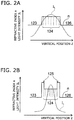
- FIG. 2A is a graph for describing the light confinement effect in a direction perpendicular to the active layer of the quantum cascade laser according to a first comparative example
- FIG. 2B is a graph for describing the light confinement effect in a direction perpendicular to the active layer of the quantum cascade laser according to a second comparative example.
- the vertical axis is the refractive index n and light intensity I L
- the horizontal axis is the vertical position Z.
- an active layer 124 is interposed by a first cladding layer 123 and a second cladding layer 126, and an optical guide layer having an effective refractive index higher than the refractive index of the injection quantum well region and the refractive index of the light-emitting quantum well region is not provided. Therefore, the light confinement effect is weak, and the distribution of light intensity I L expands to within the active layer 124. Because of this, the threshold electric current cannot be reduced, and it is difficult to achieve high output.
- a optical guide layer 125 having a refractive index higher than the effective refractive index of each of the light-emitting quantum well regions is provided between the active layer 124 and the first cladding later 123, and between the active layer 124 and the second cladding layer 126. Because the optical guide layer 125 is provided, the light confinement effect can be strengthened more than in the first comparative example, but the light confinement effect is less than in the first embodiment, wherein the optical guide layer 125 is disposed in the central portion. Note that the light confinement effect will be described in detail later using the simulation results.
- FIG. 3A is a schematic perspective view of the quantum cascade laser according to the first embodiment
- FIG. 3B is a schematic cross-sectional view along the A-A line.
- the quantum cascade laser can further have a substrate 10, and a stacked body 20 is further provided, crystal grown using a metal organic chemical vapor deposition (MOCVD) method or a molecular beam epitaxy (MBE) method.
- MOCVD metal organic chemical vapor deposition
- MBE molecular beam epitaxy
- the stacked body 20 is processed by a stripe-shaped ridge wave guide RG.
- dielectric layers 40 and 42 are provided to cover the substrate 10 and the stacked body 20. The dielectric layers 40 and 42 are opened so that the upper surface of the stacked body 20 is exposed, and a first electrode 50 is provided. Furthermore, a second electrode 52 is provided on the back surface of the substrate 10.
- a width WA of the ridge waveguide RG is, for example, 10 to 50 ⁇ m or the like. Note that in FIG. 3B , a cross-section of the ridge waveguide RG is shown by rectangles having side surfaces 20a and 20b. However, the shape of the ridge waveguide RG is not limited to this, and may be mesa-shaped.
- the stacked body 20 has a foundation layer 21, a contact layer 22, the first cladding layer 23, the active layer 24a, the optical guide layer 25, the active layer 24b, the second cladding layer 26, and a contact layer 27, in this order from the side of the substrate 10.
- laser light 60 having an infrared/terahertz wavelength is emitted from the edge surface of the active layer 24 along an optical axis 62.
- the substrate 10 includes InP or GaAs, and the light-emitting quantum well regions 80 are well layers including In x Ga 1-x As (0 ⁇ x ⁇ 1), and barrier layers including In y Al 1-y As (0 ⁇ y ⁇ 1). Furthermore, the optical guide layer 25 includes In z Ga 1-z As (0 ⁇ z ⁇ 1).
- FIG. 4A is a graph showing the simulation results of relative light intensity distribution in a first specific example of the first embodiment
- FIG. 4B is a graph showing the simulation results of threshold electric current dependency with respect to the thickness of the optical guide layer.
- the vertical axis is the refractive index (solid line) n or light intensity (broken line) I L
- the horizontal axis is the vertical position Z.
- Table 1 shows the unit stacked body 100 of the first specific example.
- Reference Numeral Layer Composition Thickness ( ⁇ m) Doping (x10 17 cm -2 ) Refractive index 21 Foundation Layer InP 3 30 2.967+j1.515E-02 22 Contact Layer In 0.532 Ga 0.468 As 1 10 3.336+j7.9E-03 23 Cladding Layer InP 2.5 0.4 3.089+j1.94E-04 24a Active layer InGaAs/InAlAs 1.1895 0.1 3.263+j1.199E-04 25 Optical Guide Layer In 0.532 Ga 0.468 As 0.3 0 3.402 24 b Active layer InGaAs/InAlAs 1.1895 0.1 3.263+j1.199E-04 26 Cladding Layer InP 2.5 0.4 3.089+j1.94E-04 27 Contact Layer In 0.532 Ga 0.468 As 1.0 10 3.336+j7.9E-03 50 Upper Electrode Au 1.0 1.425+j3.222E-01
- the stacked body 20 has the foundation layer 21 including n-type InP (thickness: 3 ⁇ m, refractive index: 2.97), the contact layer 22 including n-type InGaAs (thickness: 1 ⁇ m, refractive index: 3.34), the first cladding layer 23 including n-type InP (thickness: 2.5 ⁇ m, refractive index: 3.09), the active layer 24a (thickness: 1.19 ⁇ m, refractive index: 3.26), the optical guide layer 25 including InGaAs (thickness: 0.3 ⁇ m, refractive index: 3.4), the active layer 24b (thickness: 1.19 ⁇ m, refractive index: 3.26), the second cladding later 26 including n-type InP (thickness: 2.5 ⁇ m, refractive index: 3.09), and the contact layer 27 including n-type InGaAs (thickness: 1 ⁇ m, refractive index: 3.34), in this order from the side of the substrate 10.
- the foundation layer 21 may be a portion of the substrate 10. Note that when configuring the contact layers 22 and 27, the optical guide layer 25, the active layers 24a and 24b, and the like by In x Ga 1-x As (0 ⁇ x ⁇ 1), when the mole ratio x approaches 0.523, lattice match with InP becomes easier, and crystallinity becomes favorable.
- the light-emitting quantum well regions 80 can have two or more well layers.
- the well layer thickness TW of the thicker one is 4.5 nm or the like.
- the thickness TG of the optical guide layer 25 is 0.3 ⁇ m, and is sufficiently thicker than the well layer thickness TW. Therefore, optical transition between sub-bands does not occur in the optical guide layer 25. That is, the electron that is the carrier 102 is confined in a well layer of the light-emitting quantum well region 80.
- light is confined near the optical guide layer 25 having a refractive index higher than the effective refractive index of the light-emitting quantum well layers 80. If the well layer thickness TW is made to be 4.5 nm, the peak of gain is an infrared band such as near 3.7 ⁇ m or near 4.3 ⁇ m.
- the spreading width (stacking direction) of the laser beam in which the light intensity I L is half of the peak value can be made narrow at approximately 1.8 ⁇ m. Therefore, as shown in point A of FIG. 4B , the threshold electric current can be made low at approximately 0.392 kA/cm 2 . Because of this, the quantum efficiency and light output can be raised. Furthermore, warping may be introduced to the light-emitting quantum well regions 80.
- the well layer can be made In 0.669 Ga 0.331 As (the lattice constant number is larger than InP), and the barrier layer can be made In 0.362 AI 0.638 As (the lattice constant number is smaller than InP), or the like. When done in this manner, for example, lattice mismatch is compensated for between the well layer and the barrier layer, so crystallinity can be maintained in a favorable manner, and the threshold electric current can be further reduced.
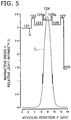
- FIG. 5 is a graph showing the simulation results of relative light intensity distribution in the second comparative example.
- the vertical axis is the refractive index (solid line) n or light intensity (broken line) I L
- the horizontal axis is the position Z in the vertical direction.
- Table 2 shows the unit stacked body of the second comparative example.
- Reference Numeral Layer Composition Thickness ( ⁇ m) Doping (x10 17 cm -2 ) Refractive index 121 Foundation Layer InP 3 30 2.967+j1.515E-02 122 Contact Layer In 0.532 Ga 0.468 As 1 10 3.336+j7.9E-03 123 Cladding Layer InP 2.5 0.4 3.089+j1.94E-04 125a
- Optical guide layer In 0.532 Ga 0.468 AS 0.3 1.0 3.395+j7.764E-04 124 Active layer InGaAs/InAlAs 2.38 0.1 3.263+j1.199E-04 125b
- Optical Guide Layer In 0.532 Ga 0.468 As 0.3 1.0 3.395+j7.764E-04 126 Cladding Layer InP 2.5 0.4 3.089+j1.94E-04 127 Contact Layer In 0.532 Ga 0.468 As 1.0 10 3.336+j7.9E-03 150
- the stacked body includes a foundation layer 121 including n-type InP (thickness: 3 ⁇ m, refractive index: 2.97), a contact layer 122 made of n-type InGaAs (thickness: 1 ⁇ m, refractive index: 3.34), the first cladding layer 123 including n-type InP (thickness: 2.5 ⁇ m, refractive index: 3.09), a optical guide layer 125a (thickness: 0.3 ⁇ m, refractive index: 3.40), the active layer 124 (thickness: 2.38 ⁇ m, refractive index: 3.26), a optical guide layer 125 b (thickness: 0.3 ⁇ m, refractive index: 3.40), the second cladding later 126 including n-type InP (thickness: 2.5 ⁇ m, refractive index: 3.09), and a contact layer 127 including n-type InGaAs (thickness: 1.0 ⁇ m, refractive index: 3.34), in this
- the spreading width (stacking direction) of the laser beam in which the light intensity I L is half of the peak value becomes wide at approximately 2.29 ⁇ m. Because of this, the threshold electric current becomes large at approximately 0.498 kA/cm 2 , and the quantum efficiency and light output are reduced lower than in the first specific example.
- FIG. 6A is a graph showing the simulation results of relative light intensity distribution in the second specific example of the first embodiment
- FIG. 6B is a graph showing the simulation results of threshold electric current dependency with respect to the thickness of a optical guide layer.
- the vertical axis shows the refractive index (solid line) n or light intensity (broken line) I L
- the horizontal axis shows the vertical position Z.
- Table 3 shows the unit stacked body 100 of the second specific example.
- Reference Numeral Layer Composition Thickness ( ⁇ m) Doping (x10 17 cm -2 ) Refractive index 21 Foundation Layer InP 3 30 2.967+j1.515E-02 23 Cladding Layer InP 2.5 0.4 3.089+j1.94E-04 24a Active layer InGaAs/InAlAs 1.1895 0.1 3.263+j1.199E-04 25 Optical Guide Layer In 0.532 Ga 0.468 AS 0.3 0 3.402 24b Active layer InGaAs/InAlAs 1.1895 0.1 3.263+j1.199E-04 26 Cladding Layer InP 2.5 0.4 3.089+j1.94E-04 27 Contact Layer In 0.532 Ga 0.468 AS 0.1 10 3.336+j7.9E-03 50 Upper Electrode Au 1.0 1.425+j3.222E-01
- the spreading width (stacking direction) of the laser beam in which the light intensity I L is half of the peak value can be made narrow at approximately 1.8 ⁇ m. Therefore, as shown in point B of FIG. 6B , the threshold electric current can be made low at approximately 0.384 kA/cm 2 . Because of this, the quantum efficiency and light output can be raised.
- FIG. 7A is a graph showing the simulation results of relative light intensity distribution in a third specific example of the first embodiment
- FIG. 7B is a graph showing the simulation results of threshold electric current dependency with respect to the thickness of a optical guide layer.
- the vertical axis shows the refractive index (solid line) n or light intensity (broken line) I L
- the horizontal axis shows the vertical position Z.
- Table 4 shows the unit stacked body of the third specific example 3.
- Reference Numeral Layer Composition Thickness ( ⁇ m) Doping (x10 17 cm -2 ) I Refractive index 21 Foundation Layer InP 3 30 2.967+j1.515E-02 23 Cladding Layer InP 2.5 0.4 3.089+j1.94E-04 24a Active layer InGaAs/InAlAs 0.6885 0.17 3.263+j1.199E-04 25 Optical Guide Layer In 0.532 Ga 0.468 As 0.3 0 3.402 24b Active layer InGaAs/InAlAs 0.6885 0.17 3.263+j1.199E-04 26 Cladding Layer InP 2.5 0.4 3.089+j1.94E-04 27 Contact Layer In 0.532 Ga 0.468 AS 0.1 10 3.336+j7.9E-03 50 Upper Electrode Au 1.0 1.425+j3.222E-01
- the stacked body 20 includes the foundation layer 21 including n-type InP (thickness: 3 ⁇ m, refractive index: 2.97), the first cladding layer 23 including n-type InP (thickness: 2.5 ⁇ m, refractive index: 3.09), the active layer 24a (thickness: 0.69 ⁇ m, refractive index: 3.29), the optical guide layer 25 (thickness: 0.3 ⁇ m, refractive index: 3.42), the active layer 24b (thickness: 0.69 ⁇ m, refractive index: 3.29), the second cladding later 26 including n-type InP (thickness: 2.5 ⁇ m, refractive index: 3.09), and the contact layer 27 including n-type InGaAs (thickness: 0.1 ⁇ m, refractive index: 3.37) in this order from the side of the substrate 10.
- the spreading width (stacking direction) of the laser beam in which the light intensity I L is half of the peak value can be made narrow at approximately 1.27 ⁇ m. Therefore, as shown in point C of FIG. 7B , the threshold electric current can be made low at approximately 0.206 kA/cm 2 . Because of this, the quantum efficiency and light output can be raised.
- a quantum cascade laser having a lower threshold electric current.
- the quantum efficiency or light output of a quantum cascade laser can be raised.
- These quantum cascade lasers can be widely used for gas analysis, environment measurement, detection of dangerous substances, and the like.
Landscapes
- Physics & Mathematics (AREA)
- Condensed Matter Physics & Semiconductors (AREA)
- General Physics & Mathematics (AREA)
- Electromagnetism (AREA)
- Optics & Photonics (AREA)
- Geometry (AREA)
- Semiconductor Lasers (AREA)
Abstract
Description
- The embodiment of the invention relates to a quantum cascade laser.
- A quantum cascade laser (QCL) emits infrared laser light.
- When a threshold electric current of a quantum cascade laser is reduced, the quantum efficiency or light output can be raised.
- However, quantum cascade lasers have an active layer in which a large number of light-emitting quantum well regions are cascade-connected thereon. Therefore, it cannot be said that optical confinement is sufficient in the direction perpendicular to a thick active layer, and it is not easy to reduce the threshold electric current.
-
-
FIG. 1A is a graph for describing light confinement in a vertical direction of the quantum cascade laser according to the first embodiment, andFIG. 1B is a graph showing the energy level of a conduction band; -
FIG. 2A is a graph for describing light confinement in a vertical direction of the quantum cascade laser according to a first comparative example, andFIG. 2B is a graph for describing light confinement in a vertical direction of the quantum cascade laser according to a second comparative example; -
FIG. 3A is a schematic perspective view of the quantum cascade laser according to the first embodiment, andFIG. 3B is a schematic cross-sectional view along the A-A line; -
FIG. 4A is a graph showing the simulation results of relative light intensity distribution in a first specific example of the first embodiment, andFIG. 4B is a graph showing the simulation results of threshold electric current dependency with respect to the thickness of an optical guide layer; -
FIG. 5 is a graph showing the simulation results of relative light intensity distribution in a specific example of a second comparative example; -
FIG. 6A is a graph showing the simulation results of relative light intensity distribution in a second specific example of the first embodiment, andFIG. 6B is a graph showing the simulation results of threshold electric current dependency with respect to the thickness of an optical guide layer; and -
FIG. 7A is a graph showing the simulation results of relative light intensity distribution in a third specific example of the first embodiment, andFIG. 7B is a graph showing the simulation results of threshold electric current dependency with respect to the thickness of an optical guide layer. - In general, according to one embodiment, a quantum cascade laser of the embodiment has an active layer, a first and second cladding layer, and an optical guide layer. The active layer has a plurality of injection quantum well regions and a plurality of light-emitting quantum well regions. Each of the injection quantum well regions and each of the light-emitting quantum well regions are alternatively stacked. The each of the light-emitting quantum well regions emit laser light by optical transition between sub-bands of a carrier. The each of the injection quantum well regions mitigate the carrier after optical transition between sub-bands to a mini-band level, and inject the carrier into the light-emitting quantum well region which is downstream. The first and second cladding layers are provided to interpose the active layer from both sides, and have a refractive index lower than an effective refractive index of each of the light-emitting quantum well regions. The optical guide layer is disposed to divide the active layer into two parts in a stacking direction. The optical guide layer has a refractive index higher than the effective refractive index of the each of the light-emitting quantum well regions, and has a thickness greater than the thickness of all well layers of quantum well layers of the each of the light-emitting quantum well regions.
- Hereinafter, embodiments of the invention will be described below with reference to drawings.
-
FIG. 1A is a graph for describing light confinement in a direction perpendicular to the active layer of the quantum cascade laser according to the first embodiment, andFIG. 1B is a graph showing the energy level of a conduction band. - In
FIG. 1A , the vertical axis shows a refractive index n (solid line) and light intensity IL (dotted line), and the horizontal axis Z shows the vertical (stacking direction) position of a semiconductor layer. As shown inFIG. 1A , the quantum cascade laser of the first embodiment has an active layer 24 (24a, 24b), afirst cladding layer 23, asecond cladding layer 26, and anoptical guide layer 25. - In
FIG. 1B , the vertical axis shows a conduction band energy level, and the horizontal axis Z shows a vertical position. As shown inFIG. 1B , theactive layer 24 has a plurality of injectionquantum well regions 90 and a plurality of light-emittingquantum well regions 80. Theactive layer 24 includes a stacked body having each injectionquantum well region 90 and each light-emittingquantum well region 80 alternatively stacked thereon. That is, a unit stackedbody 100 is arranged, including a pair of one injectionquantum well region 90 and one light-emittingquantum well region 80. That is, each of the regions interposed by the broken lines inFIG 1(a) corresponds to the unit stackedbody 100. - The number arranged is, for example, 30 to 200 or the like. Each light-emitting quantum
well region 80 emits laser light by optical transition between sub-bands of acarrier 102 such as an electron. Furthermore, each injection quantumwell region 90 mitigates thecarrier 102 after optical transition between sub-bands to a mini-band level M, and injects it into the light-emittingquantum well region 80 which is downstream. As shown inFIG. 1B , when thecarrier 102 is an electron, the electron is mitigated at a mini-band M of the injection quantum well region 90 (level A→B), emits laser light by transition between sub-bands in the light-emitting quantum well region 80 (level B→C), and is mitigated after being injected into the injectionquantum well region 90 which is downstream (level D). - The
optical guide layer 25 has a refractive index higher than the effective refractive index of each light-emittingquantum well region 80. The thickness of a well layer and thickness of a barrier layer of the light-emittingquantum well region 80 are sufficiently shorter than the wavelength of the laser light. Therefore, the effective refractive index of the light-emittingquantum well regions 80 is considered such that the medium, which is an intermediary refractive index between the refractive index of the well layer and the refractive index of the barrier layer that is lower than the refractive index of the well layer, is uniformly dispersed. Generally, a substance having a higher refractive index tends to have a lower band gap energy Eg. Even in this system, the band gap energy of theoptical guide layer 25 may be lower than the band gap energy of the quantum well layer. In a pn-junction laser diode, a substance having a small band gap energy Eg becomes a light-absorbing layer, so there is no optical guide layer provided on the central portion of the active layer. However, quantum cascade lasers emit light at a lower energy than band gap energy, so light absorption is suppressed even if a substance having a high refractive index is provided on the central portion of theactive layer 25. - It is favorable for the
optical guide layer 25 to not include quantum wells that generate optical transition between bands. Therefore, theoptical guide layer 25 has a thickness TG, which is respectively larger than the thickness of all of the well layers from among the quantum well layers of each light-emittingquantum well region 80. Note that inFIG. 1B , one light-emittingquantum well region 80 has two quantum well layers, and when the thickness of the larger well layer is expressed as TW: TG>TW. Note that if the thickness TG of theoptical guide layer 25 is 100 nm or greater, the light confinement effect can be raised, as described using a simulation hereinafter. On the other hand, if theactive layer 24a and theactive layer 24b are separated too much, the optical feedback effect is lessened. Therefore, it is favorable for the thickness TG of theoptical guide layer 25 to be 500 nm or less. - Moreover, it is favorable for the
optical guide layer 25 to be provided to divide theactive layer 24 into two substantially equal parts because this makes it so that the light intensity distribution can be close to symmetrical. For example, if the number of cascade-connected unit stackedbodies 100 is an even number, theoptical guide layer 25 may be provided to divide the stacked number of unit stackedbodies 100 into two equal parts. Furthermore, if the stacked number of unit stackedbodies 100 is an odd number, one of the sides becomes slightly larger. However, because the stacked number of unit stackedbodies 100 is large at 30 to 200 or the like, it does not strictly need to be divided in two. - The
first cladding layer 23 and thesecond cladding layer 26 are provided to interpose theactive layer 24 from both sides. The refractive index of the first and second cladding layers 23 and 26 is lower than the effective refractive index of each light-emitting quantum well region. - In the first embodiment, the light confinement effect can be strengthened by disposing the
optical guide layer 25 around the vicinity of the central portion of theactive layer 24. Therefore, the threshold electric current is reduced, and the quantum efficiency and light output can be raised. -
FIG. 2A is a graph for describing the light confinement effect in a direction perpendicular to the active layer of the quantum cascade laser according to a first comparative example, andFIG. 2B is a graph for describing the light confinement effect in a direction perpendicular to the active layer of the quantum cascade laser according to a second comparative example. - In
FIGS. 2A and 2B , the vertical axis is the refractive index n and light intensity IL, and the horizontal axis is the vertical position Z. In the quantum cascade laser of the first comparative example shown inFIG. 2A , anactive layer 124 is interposed by afirst cladding layer 123 and asecond cladding layer 126, and an optical guide layer having an effective refractive index higher than the refractive index of the injection quantum well region and the refractive index of the light-emitting quantum well region is not provided. Therefore, the light confinement effect is weak, and the distribution of light intensity IL expands to within theactive layer 124. Because of this, the threshold electric current cannot be reduced, and it is difficult to achieve high output. - In the quantum cascade laser of the second comparative example shown in
FIG. 2B , aoptical guide layer 125 having a refractive index higher than the effective refractive index of each of the light-emitting quantum well regions is provided between theactive layer 124 and the first cladding later 123, and between theactive layer 124 and thesecond cladding layer 126. Because theoptical guide layer 125 is provided, the light confinement effect can be strengthened more than in the first comparative example, but the light confinement effect is less than in the first embodiment, wherein theoptical guide layer 125 is disposed in the central portion. Note that the light confinement effect will be described in detail later using the simulation results. -
FIG. 3A is a schematic perspective view of the quantum cascade laser according to the first embodiment, andFIG. 3B is a schematic cross-sectional view along the A-A line. - The quantum cascade laser can further have a
substrate 10, and astacked body 20 is further provided, crystal grown using a metal organic chemical vapor deposition (MOCVD) method or a molecular beam epitaxy (MBE) method. Thestacked body 20 is processed by a stripe-shaped ridge wave guide RG. Additionally,dielectric layers substrate 10 and thestacked body 20. The dielectric layers 40 and 42 are opened so that the upper surface of the stackedbody 20 is exposed, and afirst electrode 50 is provided. Furthermore, asecond electrode 52 is provided on the back surface of thesubstrate 10. - A width WA of the ridge waveguide RG is, for example, 10 to 50 µm or the like. Note that in
FIG. 3B , a cross-section of the ridge waveguide RG is shown by rectangles havingside surfaces - The
stacked body 20 has afoundation layer 21, acontact layer 22, thefirst cladding layer 23, theactive layer 24a, theoptical guide layer 25, theactive layer 24b, thesecond cladding layer 26, and acontact layer 27, in this order from the side of thesubstrate 10. - As illustrated in
FIG. 3A ,laser light 60 having an infrared/terahertz wavelength is emitted from the edge surface of theactive layer 24 along anoptical axis 62. - Next, the light intensity distribution and threshold electric current calculated by a simulation will be described as a specific example. The
substrate 10 includes InP or GaAs, and the light-emitting quantum wellregions 80 are well layers including InxGa1-xAs (0<x<1), and barrier layers including InyAl1-yAs (0<y<1). Furthermore, theoptical guide layer 25 includes InzGa1-zAs (0<z<1). -
FIG. 4A is a graph showing the simulation results of relative light intensity distribution in a first specific example of the first embodiment, andFIG. 4B is a graph showing the simulation results of threshold electric current dependency with respect to the thickness of the optical guide layer. - In
FIG. 4A , the vertical axis is the refractive index (solid line) n or light intensity (broken line) IL, and the horizontal axis is the vertical position Z. - (Table 1) shows the unit stacked
body 100 of the first specific example.[Table 1] Reference Numeral Layer Composition Thickness (µm) Doping (x1017cm-2) Refractive index 21 Foundation Layer InP 3 30 2.967+j1.515E-02 22 Contact Layer In0.532Ga0.468As 1 10 3.336+j7.9E-03 23 Cladding Layer InP 2.5 0.4 3.089+j1.94E-04 24a Active layer InGaAs/InAlAs 1.1895 0.1 3.263+j1.199E-04 25 Optical Guide Layer In0.532Ga0.468As 0.3 0 3.402 24 b Active layer InGaAs/InAlAs 1.1895 0.1 3.263+j1.199E-04 26 Cladding Layer InP 2.5 0.4 3.089+j1.94E-04 27 Contact Layer In0.532Ga0.468As 1.0 10 3.336+j7.9E-03 50 Upper Electrode Au 1.0 1.425+j3.222E-01 - The
stacked body 20 has thefoundation layer 21 including n-type InP (thickness: 3 µm, refractive index: 2.97), thecontact layer 22 including n-type InGaAs (thickness: 1 µm, refractive index: 3.34), thefirst cladding layer 23 including n-type InP (thickness: 2.5 µm, refractive index: 3.09), theactive layer 24a (thickness: 1.19 µm, refractive index: 3.26), theoptical guide layer 25 including InGaAs (thickness: 0.3 µm, refractive index: 3.4), theactive layer 24b (thickness: 1.19 µm, refractive index: 3.26), the second cladding later 26 including n-type InP (thickness: 2.5 µm, refractive index: 3.09), and thecontact layer 27 including n-type InGaAs (thickness: 1 µm, refractive index: 3.34), in this order from the side of thesubstrate 10. Note that thefoundation layer 21 may be a portion of thesubstrate 10. Note that when configuring the contact layers 22 and 27, theoptical guide layer 25, theactive layers - As shown in
FIG. 1B , the light-emitting quantum wellregions 80 can have two or more well layers. For example, the well layer thickness TW of the thicker one is 4.5 nm or the like. The thickness TG of theoptical guide layer 25 is 0.3 µm, and is sufficiently thicker than the well layer thickness TW. Therefore, optical transition between sub-bands does not occur in theoptical guide layer 25. That is, the electron that is thecarrier 102 is confined in a well layer of the light-emittingquantum well region 80. On the other hand, light is confined near theoptical guide layer 25 having a refractive index higher than the effective refractive index of the light-emitting quantum well layers 80. If the well layer thickness TW is made to be 4.5 nm, the peak of gain is an infrared band such as near 3.7 µm or near 4.3 µm. - As shown in
FIG. 4A , the spreading width (stacking direction) of the laser beam in which the light intensity IL is half of the peak value can be made narrow at approximately 1.8 µm. Therefore, as shown in point A ofFIG. 4B , the threshold electric current can be made low at approximately 0.392 kA/cm2. Because of this, the quantum efficiency and light output can be raised. Furthermore, warping may be introduced to the light-emitting quantum wellregions 80. For example, the well layer can be made In0.669Ga0.331As (the lattice constant number is larger than InP), and the barrier layer can be made In0.362AI0.638As (the lattice constant number is smaller than InP), or the like. When done in this manner, for example, lattice mismatch is compensated for between the well layer and the barrier layer, so crystallinity can be maintained in a favorable manner, and the threshold electric current can be further reduced. -
FIG. 5 is a graph showing the simulation results of relative light intensity distribution in the second comparative example. - In
FIG. 5 , the vertical axis is the refractive index (solid line) n or light intensity (broken line) IL, and the horizontal axis is the position Z in the vertical direction. - (Table 2) shows the unit stacked body of the second comparative example.
[Table 2] Reference Numeral Layer Composition Thickness (µm) Doping (x1017cm-2) Refractive index 121 Foundation Layer InP 3 30 2.967+j1.515E-02 122 Contact Layer In0.532Ga0.468As 1 10 3.336+j7.9E-03 123 Cladding Layer InP 2.5 0.4 3.089+j1.94E-04 125a Optical guide layer In0.532Ga0.468AS 0.3 1.0 3.395+j7.764E-04 124 Active layer InGaAs/InAlAs 2.38 0.1 3.263+j1.199E-04 125b Optical Guide Layer In0.532Ga0.468As 0.3 1.0 3.395+j7.764E-04 126 Cladding Layer InP 2.5 0.4 3.089+j1.94E-04 127 Contact Layer In0.532Ga0.468As 1.0 10 3.336+j7.9E-03 150 Upper Electrode Au 1.0 1.425+j3.222E-01 - The stacked body includes a
foundation layer 121 including n-type InP (thickness: 3 µm, refractive index: 2.97), acontact layer 122 made of n-type InGaAs (thickness: 1 µm, refractive index: 3.34), thefirst cladding layer 123 including n-type InP (thickness: 2.5 µm, refractive index: 3.09), aoptical guide layer 125a (thickness: 0.3 µm, refractive index: 3.40), the active layer 124 (thickness: 2.38 µm, refractive index: 3.26), aoptical guide layer 125 b (thickness: 0.3 µm, refractive index: 3.40), the second cladding later 126 including n-type InP (thickness: 2.5 µm, refractive index: 3.09), and acontact layer 127 including n-type InGaAs (thickness: 1.0 µm, refractive index: 3.34), in this order from the side of the substrate. - The spreading width (stacking direction) of the laser beam in which the light intensity IL is half of the peak value becomes wide at approximately 2.29 µm. Because of this, the threshold electric current becomes large at approximately 0.498 kA/cm2, and the quantum efficiency and light output are reduced lower than in the first specific example.
-
FIG. 6A is a graph showing the simulation results of relative light intensity distribution in the second specific example of the first embodiment, andFIG. 6B is a graph showing the simulation results of threshold electric current dependency with respect to the thickness of a optical guide layer. - In
FIG. 6A , the vertical axis shows the refractive index (solid line) n or light intensity (broken line) IL, and the horizontal axis shows the vertical position Z. - (Table 3) shows the unit stacked
body 100 of the second specific example.[Table 3] Reference Numeral Layer Composition Thickness (µm) Doping (x1017cm-2) Refractive index 21 Foundation Layer InP 3 30 2.967+j1.515E-02 23 Cladding Layer InP 2.5 0.4 3.089+j1.94E-04 24a Active layer InGaAs/InAlAs 1.1895 0.1 3.263+j1.199E-04 25 Optical Guide Layer In0.532Ga0.468AS 0.3 0 3.402 24b Active layer InGaAs/InAlAs 1.1895 0.1 3.263+j1.199E-04 26 Cladding Layer InP 2.5 0.4 3.089+j1.94E-04 27 Contact Layer In0.532Ga0.468AS 0.1 10 3.336+j7.9E-03 50 Upper Electrode Au 1.0 1.425+j3.222E-01 - In the
stacked body 20, thefoundation layer 21 including n-type InP (thickness: 3 µm, refractive index: 2.97), thefirst cladding layer 23 including n-type InP (thickness: 2.5 µm, refractive index: 3.09), theactive layer 24a (thickness: 1.19 µm, refractive index: 3.26), the optical guide layer 25 (thickness: 0.3 µm, refractive index: 3.4), theactive layer 24b (thickness: 1.19 µm, refractive index: 3.26), the second cladding later 26 including n-type InP (thickness: 2.5 µm, refractive index: 3.09), and thecontact layer 27 including n-type InGaAs (thickness: 0.1 µm, refractive index: 3.34), are disposed from the side of thesubstrate 10. - As shown in
FIG. 6A , the spreading width (stacking direction) of the laser beam in which the light intensity IL is half of the peak value can be made narrow at approximately 1.8 µm. Therefore, as shown in point B ofFIG. 6B , the threshold electric current can be made low at approximately 0.384 kA/cm2. Because of this, the quantum efficiency and light output can be raised. -
FIG. 7A is a graph showing the simulation results of relative light intensity distribution in a third specific example of the first embodiment, andFIG. 7B is a graph showing the simulation results of threshold electric current dependency with respect to the thickness of a optical guide layer. - In
FIG. 7A , the vertical axis shows the refractive index (solid line) n or light intensity (broken line) IL, and the horizontal axis shows the vertical position Z. - (Table 4) shows the unit stacked body of the third specific example 3.
[Table 4] Reference Numeral Layer Composition Thickness (µm) Doping (x1017cm-2) I Refractive index 21 Foundation Layer InP 3 30 2.967+j1.515E-02 23 Cladding Layer InP 2.5 0.4 3.089+j1.94E-04 24a Active layer InGaAs/InAlAs 0.6885 0.17 3.263+j1.199E-04 25 Optical Guide Layer In0.532Ga0.468As 0.3 0 3.402 24b Active layer InGaAs/InAlAs 0.6885 0.17 3.263+j1.199E-04 26 Cladding Layer InP 2.5 0.4 3.089+j1.94E-04 27 Contact Layer In0.532Ga0.468AS 0.1 10 3.336+j7.9E-03 50 Upper Electrode Au 1.0 1.425+j3.222E-01 - The
stacked body 20 includes thefoundation layer 21 including n-type InP (thickness: 3 µm, refractive index: 2.97), thefirst cladding layer 23 including n-type InP (thickness: 2.5 µm, refractive index: 3.09), theactive layer 24a (thickness: 0.69 µm, refractive index: 3.29), the optical guide layer 25 (thickness: 0.3 µm, refractive index: 3.42), theactive layer 24b (thickness: 0.69 µm, refractive index: 3.29), the second cladding later 26 including n-type InP (thickness: 2.5 µm, refractive index: 3.09), and thecontact layer 27 including n-type InGaAs (thickness: 0.1 µm, refractive index: 3.37) in this order from the side of thesubstrate 10. - As shown in
FIG. 7A , the spreading width (stacking direction) of the laser beam in which the light intensity IL is half of the peak value can be made narrow at approximately 1.27 µm. Therefore, as shown in point C ofFIG. 7B , the threshold electric current can be made low at approximately 0.206 kA/cm2. Because of this, the quantum efficiency and light output can be raised. - According to the embodiment, a quantum cascade laser is provided having a lower threshold electric current. By making a low threshold electric current, the quantum efficiency or light output of a quantum cascade laser can be raised. These quantum cascade lasers can be widely used for gas analysis, environment measurement, detection of dangerous substances, and the like.
- While certain embodiments have been described, these embodiments have been presented by way of example only, and are not intended to limit the scope of the inventions. Indeed, the novel embodiments described herein may be embodied in a variety of other forms; furthermore, various omissions, substitutions and changes in the form of the embodiments described herein may be made without departing from the spirit of the inventions. The accompanying claims and their equivalents are intended to cover such forms or modification as would fall within the scope and spirit of the inventions.
Claims (5)
- A quantum cascade laser comprising:an active layer (24) including a plurality of injection quantum well regions (90) and a plurality of light-emitting quantum well regions (80), the each of the plurality of injection quantum well regions (90) and the each of the plurality of light-emitting quantum well regions (80) being alternatively stacked, the each of the plurality of light-emitting quantum well regions (80) emitting laser light by optical transition between sub-bands of a carrier, and the each of the plurality of injection quantum well regions (90) mitigating the carrier (102) after the optical transition between sub-bands to a mini-band level, and injecting the carrier (102) into a light-emitting quantum well region (80) downstream;a first and a second cladding layer (23, 26) provided interposing the active layer (24) from both sides, having a refractive index lower than an effective refractive index of the each of the plurality of light-emitting quantum well regions (80); andan optical guide layer (25) disposed dividing the active layer (24) into two parts in a stacking direction, having a refractive index higher than the effective refractive index of the each of the plurality of light-emitting quantum well regions (80), and having a thickness greater than a thickness of all well layers of quantum well layers of the each of the plurality of light-emitting quantum well regions (80).
- The laser according to claim 1, wherein the optical guide layer (25) is provided dividing the active layer (24) into two substantially equal parts in the stacking direction.
- The laser according to claim 1 or 2, further comprising a substrate (10),
the first and the second cladding layers (23, 26) including a material that lattice-matches the substrate (10). - The laser according to one of claims 1-3, wherein the thickness of the optical guide layer (25) is 100 nm or greater and 500 nm or less.
- The laser according to one of claims 1-4, wherein:the substrate (10) includes InP,
each of the plurality of light-emitting quantum well regions (80) includes a well layer including InxGa1-xAs, and a barrier layer including InyAl1-yAs, however 0<x<1 and 0<y<1,
the optical guide layer (25) includes InzGa1-zAs, however 0<z<1, and
the first cladding layer (23) and the second cladding layer (26) include InP
Priority Applications (1)
| Application Number | Priority Date | Filing Date | Title |
|---|---|---|---|
| EP17210685.8A EP3506439B1 (en) | 2017-12-27 | 2017-12-27 | Quantum cascade laser |
Applications Claiming Priority (1)
| Application Number | Priority Date | Filing Date | Title |
|---|---|---|---|
| EP17210685.8A EP3506439B1 (en) | 2017-12-27 | 2017-12-27 | Quantum cascade laser |
Publications (2)
| Publication Number | Publication Date |
|---|---|
| EP3506439A1 true EP3506439A1 (en) | 2019-07-03 |
| EP3506439B1 EP3506439B1 (en) | 2021-03-31 |
Family
ID=61249469
Family Applications (1)
| Application Number | Title | Priority Date | Filing Date |
|---|---|---|---|
| EP17210685.8A Active EP3506439B1 (en) | 2017-12-27 | 2017-12-27 | Quantum cascade laser |
Country Status (1)
| Country | Link |
|---|---|
| EP (1) | EP3506439B1 (en) |
Cited By (1)
| Publication number | Priority date | Publication date | Assignee | Title |
|---|---|---|---|---|
| DE102024106171A1 (en) | 2023-03-06 | 2024-09-12 | Justus-Liebig-Universität Gießen, Körperschaft des öffentlichen Rechts | Semiconductor laser with semiconductor material system with Fermi level control by doping the active region at spatially indirect transitions |
Citations (3)
| Publication number | Priority date | Publication date | Assignee | Title |
|---|---|---|---|---|
| US20040066823A1 (en) * | 2002-09-30 | 2004-04-08 | Federico Capasso | Nonlinear semiconductor light sources |
| US20070008999A1 (en) * | 2004-06-07 | 2007-01-11 | Maxion Technologies, Inc. | Broadened waveguide for interband cascade lasers |
| US20130195136A1 (en) * | 2011-08-03 | 2013-08-01 | Kabushiki Kaisha Toshiba | Semiconductor laser |
-
2017
- 2017-12-27 EP EP17210685.8A patent/EP3506439B1/en active Active
Patent Citations (3)
| Publication number | Priority date | Publication date | Assignee | Title |
|---|---|---|---|---|
| US20040066823A1 (en) * | 2002-09-30 | 2004-04-08 | Federico Capasso | Nonlinear semiconductor light sources |
| US20070008999A1 (en) * | 2004-06-07 | 2007-01-11 | Maxion Technologies, Inc. | Broadened waveguide for interband cascade lasers |
| US20130195136A1 (en) * | 2011-08-03 | 2013-08-01 | Kabushiki Kaisha Toshiba | Semiconductor laser |
Cited By (2)
| Publication number | Priority date | Publication date | Assignee | Title |
|---|---|---|---|---|
| DE102024106171A1 (en) | 2023-03-06 | 2024-09-12 | Justus-Liebig-Universität Gießen, Körperschaft des öffentlichen Rechts | Semiconductor laser with semiconductor material system with Fermi level control by doping the active region at spatially indirect transitions |
| DE102024106171B4 (en) | 2023-03-06 | 2025-01-02 | Justus-Liebig-Universität Gießen, Körperschaft des öffentlichen Rechts | Semiconductor laser with semiconductor material system with Fermi level control by doping the active region at spatially indirect transitions |
Also Published As
| Publication number | Publication date |
|---|---|
| EP3506439B1 (en) | 2021-03-31 |
Similar Documents
| Publication | Publication Date | Title |
|---|---|---|
| US10038308B2 (en) | Quantum cascade semiconductor laser | |
| US7756179B2 (en) | Semiconductor laser apparatus | |
| US20210376571A1 (en) | Semiconductor device, semiconductor laser, and method of producing a semiconductor device | |
| US20130195136A1 (en) | Semiconductor laser | |
| US4701774A (en) | Light emitting semiconductor device | |
| JP7689112B2 (en) | Two-dimensional photonic crystal laser | |
| US8304757B2 (en) | Semiconductor light-emitting device, optical module, transmitter, and optical communication system | |
| US8437375B2 (en) | Semiconductor laser element | |
| US20070008999A1 (en) | Broadened waveguide for interband cascade lasers | |
| JP3872398B2 (en) | Light emitting device manufacturing method and light emitting device | |
| JP6557649B2 (en) | Quantum cascade laser | |
| EP3506439B1 (en) | Quantum cascade laser | |
| US8660160B2 (en) | Semiconductor laser element and method of manufacturing the same | |
| US11258233B2 (en) | Quantum cascade laser | |
| CN216529835U (en) | 940nm vertical cavity surface emitting laser epitaxial wafer | |
| WO2023243518A1 (en) | Nitride-based semiconductor light-emitting device | |
| CN110021878B (en) | Quantum Cascade Laser | |
| Zou et al. | Very-low-threshold, strained In/sub y/Ga/sub 1-y/As-GaAs quantum-well lasers defined by impurity-induced disordering | |
| TWI667854B (en) | Quantum cascade laser | |
| US11600969B2 (en) | Quantum cascade laser element | |
| WO2010022526A2 (en) | Superluminescent diode, or amplifier chip | |
| US7724794B2 (en) | Semiconductor laser device | |
| US20070064757A1 (en) | Avalanche quantum intersubband transition semiconductor laser | |
| Martin et al. | All-optical modulation near 1.55 µm usmg Ini-x-yGaxAlyAs coupled quantum wells | |
| Getty et al. | Segmented 1.55/spl mu/m laser with 400% differential quantum efficiency |
Legal Events
| Date | Code | Title | Description |
|---|---|---|---|
| PUAI | Public reference made under article 153(3) epc to a published international application that has entered the european phase |
Free format text: ORIGINAL CODE: 0009012 |
|
| STAA | Information on the status of an ep patent application or granted ep patent |
Free format text: STATUS: REQUEST FOR EXAMINATION WAS MADE |
|
| 17P | Request for examination filed |
Effective date: 20171227 |
|
| AK | Designated contracting states |
Kind code of ref document: A1 Designated state(s): AL AT BE BG CH CY CZ DE DK EE ES FI FR GB GR HR HU IE IS IT LI LT LU LV MC MK MT NL NO PL PT RO RS SE SI SK SM TR |
|
| AX | Request for extension of the european patent |
Extension state: BA ME |
|
| STAA | Information on the status of an ep patent application or granted ep patent |
Free format text: STATUS: EXAMINATION IS IN PROGRESS |
|
| 17Q | First examination report despatched |
Effective date: 20200511 |
|
| GRAP | Despatch of communication of intention to grant a patent |
Free format text: ORIGINAL CODE: EPIDOSNIGR1 |
|
| STAA | Information on the status of an ep patent application or granted ep patent |
Free format text: STATUS: GRANT OF PATENT IS INTENDED |
|
| RIC1 | Information provided on ipc code assigned before grant |
Ipc: H01S 5/34 20060101AFI20201008BHEP Ipc: H01S 5/20 20060101ALI20201008BHEP Ipc: H01S 5/32 20060101ALN20201008BHEP Ipc: H01S 5/227 20060101ALN20201008BHEP Ipc: H01S 5/22 20060101ALN20201008BHEP Ipc: H01S 5/40 20060101ALN20201008BHEP |
|
| INTG | Intention to grant announced |
Effective date: 20201103 |
|
| GRAS | Grant fee paid |
Free format text: ORIGINAL CODE: EPIDOSNIGR3 |
|
| GRAA | (expected) grant |
Free format text: ORIGINAL CODE: 0009210 |
|
| STAA | Information on the status of an ep patent application or granted ep patent |
Free format text: STATUS: THE PATENT HAS BEEN GRANTED |
|
| AK | Designated contracting states |
Kind code of ref document: B1 Designated state(s): AL AT BE BG CH CY CZ DE DK EE ES FI FR GB GR HR HU IE IS IT LI LT LU LV MC MK MT NL NO PL PT RO RS SE SI SK SM TR |
|
| REG | Reference to a national code |
Ref country code: GB Ref legal event code: FG4D Ref country code: CH Ref legal event code: EP |
|
| REG | Reference to a national code |
Ref country code: DE Ref legal event code: R096 Ref document number: 602017035604 Country of ref document: DE Ref country code: AT Ref legal event code: REF Ref document number: 1378013 Country of ref document: AT Kind code of ref document: T Effective date: 20210415 |
|
| REG | Reference to a national code |
Ref country code: IE Ref legal event code: FG4D |
|
| REG | Reference to a national code |
Ref country code: NL Ref legal event code: FP |
|
| REG | Reference to a national code |
Ref country code: LT Ref legal event code: MG9D |
|
| PG25 | Lapsed in a contracting state [announced via postgrant information from national office to epo] |
Ref country code: NO Free format text: LAPSE BECAUSE OF FAILURE TO SUBMIT A TRANSLATION OF THE DESCRIPTION OR TO PAY THE FEE WITHIN THE PRESCRIBED TIME-LIMIT Effective date: 20210630 Ref country code: FI Free format text: LAPSE BECAUSE OF FAILURE TO SUBMIT A TRANSLATION OF THE DESCRIPTION OR TO PAY THE FEE WITHIN THE PRESCRIBED TIME-LIMIT Effective date: 20210331 Ref country code: HR Free format text: LAPSE BECAUSE OF FAILURE TO SUBMIT A TRANSLATION OF THE DESCRIPTION OR TO PAY THE FEE WITHIN THE PRESCRIBED TIME-LIMIT Effective date: 20210331 Ref country code: BG Free format text: LAPSE BECAUSE OF FAILURE TO SUBMIT A TRANSLATION OF THE DESCRIPTION OR TO PAY THE FEE WITHIN THE PRESCRIBED TIME-LIMIT Effective date: 20210630 |
|
| PG25 | Lapsed in a contracting state [announced via postgrant information from national office to epo] |
Ref country code: LV Free format text: LAPSE BECAUSE OF FAILURE TO SUBMIT A TRANSLATION OF THE DESCRIPTION OR TO PAY THE FEE WITHIN THE PRESCRIBED TIME-LIMIT Effective date: 20210331 Ref country code: RS Free format text: LAPSE BECAUSE OF FAILURE TO SUBMIT A TRANSLATION OF THE DESCRIPTION OR TO PAY THE FEE WITHIN THE PRESCRIBED TIME-LIMIT Effective date: 20210331 Ref country code: SE Free format text: LAPSE BECAUSE OF FAILURE TO SUBMIT A TRANSLATION OF THE DESCRIPTION OR TO PAY THE FEE WITHIN THE PRESCRIBED TIME-LIMIT Effective date: 20210331 |
|
| REG | Reference to a national code |
Ref country code: AT Ref legal event code: MK05 Ref document number: 1378013 Country of ref document: AT Kind code of ref document: T Effective date: 20210331 |
|
| PG25 | Lapsed in a contracting state [announced via postgrant information from national office to epo] |
Ref country code: SM Free format text: LAPSE BECAUSE OF FAILURE TO SUBMIT A TRANSLATION OF THE DESCRIPTION OR TO PAY THE FEE WITHIN THE PRESCRIBED TIME-LIMIT Effective date: 20210331 Ref country code: AT Free format text: LAPSE BECAUSE OF FAILURE TO SUBMIT A TRANSLATION OF THE DESCRIPTION OR TO PAY THE FEE WITHIN THE PRESCRIBED TIME-LIMIT Effective date: 20210331 Ref country code: EE Free format text: LAPSE BECAUSE OF FAILURE TO SUBMIT A TRANSLATION OF THE DESCRIPTION OR TO PAY THE FEE WITHIN THE PRESCRIBED TIME-LIMIT Effective date: 20210331 Ref country code: CZ Free format text: LAPSE BECAUSE OF FAILURE TO SUBMIT A TRANSLATION OF THE DESCRIPTION OR TO PAY THE FEE WITHIN THE PRESCRIBED TIME-LIMIT Effective date: 20210331 Ref country code: LT Free format text: LAPSE BECAUSE OF FAILURE TO SUBMIT A TRANSLATION OF THE DESCRIPTION OR TO PAY THE FEE WITHIN THE PRESCRIBED TIME-LIMIT Effective date: 20210331 |
|
| PG25 | Lapsed in a contracting state [announced via postgrant information from national office to epo] |
Ref country code: PT Free format text: LAPSE BECAUSE OF FAILURE TO SUBMIT A TRANSLATION OF THE DESCRIPTION OR TO PAY THE FEE WITHIN THE PRESCRIBED TIME-LIMIT Effective date: 20210802 Ref country code: PL Free format text: LAPSE BECAUSE OF FAILURE TO SUBMIT A TRANSLATION OF THE DESCRIPTION OR TO PAY THE FEE WITHIN THE PRESCRIBED TIME-LIMIT Effective date: 20210331 Ref country code: RO Free format text: LAPSE BECAUSE OF FAILURE TO SUBMIT A TRANSLATION OF THE DESCRIPTION OR TO PAY THE FEE WITHIN THE PRESCRIBED TIME-LIMIT Effective date: 20210331 Ref country code: SK Free format text: LAPSE BECAUSE OF FAILURE TO SUBMIT A TRANSLATION OF THE DESCRIPTION OR TO PAY THE FEE WITHIN THE PRESCRIBED TIME-LIMIT Effective date: 20210331 Ref country code: IS Free format text: LAPSE BECAUSE OF FAILURE TO SUBMIT A TRANSLATION OF THE DESCRIPTION OR TO PAY THE FEE WITHIN THE PRESCRIBED TIME-LIMIT Effective date: 20210731 |
|
| REG | Reference to a national code |
Ref country code: DE Ref legal event code: R097 Ref document number: 602017035604 Country of ref document: DE |
|
| PG25 | Lapsed in a contracting state [announced via postgrant information from national office to epo] |
Ref country code: DK Free format text: LAPSE BECAUSE OF FAILURE TO SUBMIT A TRANSLATION OF THE DESCRIPTION OR TO PAY THE FEE WITHIN THE PRESCRIBED TIME-LIMIT Effective date: 20210331 Ref country code: AL Free format text: LAPSE BECAUSE OF FAILURE TO SUBMIT A TRANSLATION OF THE DESCRIPTION OR TO PAY THE FEE WITHIN THE PRESCRIBED TIME-LIMIT Effective date: 20210331 Ref country code: ES Free format text: LAPSE BECAUSE OF FAILURE TO SUBMIT A TRANSLATION OF THE DESCRIPTION OR TO PAY THE FEE WITHIN THE PRESCRIBED TIME-LIMIT Effective date: 20210331 |
|
| PLBE | No opposition filed within time limit |
Free format text: ORIGINAL CODE: 0009261 |
|
| STAA | Information on the status of an ep patent application or granted ep patent |
Free format text: STATUS: NO OPPOSITION FILED WITHIN TIME LIMIT |
|
| 26N | No opposition filed |
Effective date: 20220104 |
|
| PG25 | Lapsed in a contracting state [announced via postgrant information from national office to epo] |
Ref country code: IS Free format text: LAPSE BECAUSE OF FAILURE TO SUBMIT A TRANSLATION OF THE DESCRIPTION OR TO PAY THE FEE WITHIN THE PRESCRIBED TIME-LIMIT Effective date: 20210731 |
|
| PG25 | Lapsed in a contracting state [announced via postgrant information from national office to epo] |
Ref country code: MC Free format text: LAPSE BECAUSE OF FAILURE TO SUBMIT A TRANSLATION OF THE DESCRIPTION OR TO PAY THE FEE WITHIN THE PRESCRIBED TIME-LIMIT Effective date: 20210331 Ref country code: IT Free format text: LAPSE BECAUSE OF FAILURE TO SUBMIT A TRANSLATION OF THE DESCRIPTION OR TO PAY THE FEE WITHIN THE PRESCRIBED TIME-LIMIT Effective date: 20210331 |
|
| REG | Reference to a national code |
Ref country code: CH Ref legal event code: PL |
|
| GBPC | Gb: european patent ceased through non-payment of renewal fee |
Effective date: 20211227 |
|
| REG | Reference to a national code |
Ref country code: BE Ref legal event code: MM Effective date: 20211231 |
|
| PG25 | Lapsed in a contracting state [announced via postgrant information from national office to epo] |
Ref country code: LU Free format text: LAPSE BECAUSE OF NON-PAYMENT OF DUE FEES Effective date: 20211227 Ref country code: IE Free format text: LAPSE BECAUSE OF NON-PAYMENT OF DUE FEES Effective date: 20211227 Ref country code: GB Free format text: LAPSE BECAUSE OF NON-PAYMENT OF DUE FEES Effective date: 20211227 |
|
| PG25 | Lapsed in a contracting state [announced via postgrant information from national office to epo] |
Ref country code: FR Free format text: LAPSE BECAUSE OF NON-PAYMENT OF DUE FEES Effective date: 20211231 Ref country code: BE Free format text: LAPSE BECAUSE OF NON-PAYMENT OF DUE FEES Effective date: 20211231 |
|
| PG25 | Lapsed in a contracting state [announced via postgrant information from national office to epo] |
Ref country code: LI Free format text: LAPSE BECAUSE OF NON-PAYMENT OF DUE FEES Effective date: 20211231 Ref country code: CH Free format text: LAPSE BECAUSE OF NON-PAYMENT OF DUE FEES Effective date: 20211231 |
|
| PG25 | Lapsed in a contracting state [announced via postgrant information from national office to epo] |
Ref country code: CY Free format text: LAPSE BECAUSE OF FAILURE TO SUBMIT A TRANSLATION OF THE DESCRIPTION OR TO PAY THE FEE WITHIN THE PRESCRIBED TIME-LIMIT Effective date: 20210331 |
|
| PG25 | Lapsed in a contracting state [announced via postgrant information from national office to epo] |
Ref country code: HU Free format text: LAPSE BECAUSE OF FAILURE TO SUBMIT A TRANSLATION OF THE DESCRIPTION OR TO PAY THE FEE WITHIN THE PRESCRIBED TIME-LIMIT; INVALID AB INITIO Effective date: 20171227 Ref country code: GR Free format text: LAPSE BECAUSE OF FAILURE TO SUBMIT A TRANSLATION OF THE DESCRIPTION OR TO PAY THE FEE WITHIN THE PRESCRIBED TIME-LIMIT Effective date: 20210331 |
|
| PG25 | Lapsed in a contracting state [announced via postgrant information from national office to epo] |
Ref country code: MK Free format text: LAPSE BECAUSE OF FAILURE TO SUBMIT A TRANSLATION OF THE DESCRIPTION OR TO PAY THE FEE WITHIN THE PRESCRIBED TIME-LIMIT Effective date: 20210331 |
|
| PG25 | Lapsed in a contracting state [announced via postgrant information from national office to epo] |
Ref country code: TR Free format text: LAPSE BECAUSE OF FAILURE TO SUBMIT A TRANSLATION OF THE DESCRIPTION OR TO PAY THE FEE WITHIN THE PRESCRIBED TIME-LIMIT Effective date: 20210331 |
|
| PG25 | Lapsed in a contracting state [announced via postgrant information from national office to epo] |
Ref country code: MT Free format text: LAPSE BECAUSE OF FAILURE TO SUBMIT A TRANSLATION OF THE DESCRIPTION OR TO PAY THE FEE WITHIN THE PRESCRIBED TIME-LIMIT Effective date: 20210331 |
|
| PGFP | Annual fee paid to national office [announced via postgrant information from national office to epo] |
Ref country code: NL Payment date: 20251003 Year of fee payment: 9 |
|
| PGFP | Annual fee paid to national office [announced via postgrant information from national office to epo] |
Ref country code: DE Payment date: 20250930 Year of fee payment: 9 |