EP3506339A1 - Micro device transfer head and related method - Google Patents
Micro device transfer head and related method Download PDFInfo
- Publication number
- EP3506339A1 EP3506339A1 EP18162804.1A EP18162804A EP3506339A1 EP 3506339 A1 EP3506339 A1 EP 3506339A1 EP 18162804 A EP18162804 A EP 18162804A EP 3506339 A1 EP3506339 A1 EP 3506339A1
- Authority
- EP
- European Patent Office
- Prior art keywords
- side arm
- arm
- micro device
- transfer head
- base
- Prior art date
- Legal status (The legal status is an assumption and is not a legal conclusion. Google has not performed a legal analysis and makes no representation as to the accuracy of the status listed.)
- Granted
Links
Images



Classifications
-
- B—PERFORMING OPERATIONS; TRANSPORTING
- B81—MICROSTRUCTURAL TECHNOLOGY
- B81C—PROCESSES OR APPARATUS SPECIALLY ADAPTED FOR THE MANUFACTURE OR TREATMENT OF MICROSTRUCTURAL DEVICES OR SYSTEMS
- B81C99/00—Subject matter not provided for in other groups of this subclass
- B81C99/0005—Apparatus specially adapted for the manufacture or treatment of microstructural devices or systems, or methods for manufacturing the same
- B81C99/002—Apparatus for assembling MEMS, e.g. micromanipulators
-
- H—ELECTRICITY
- H10—SEMICONDUCTOR DEVICES; ELECTRIC SOLID-STATE DEVICES NOT OTHERWISE PROVIDED FOR
- H10P—GENERIC PROCESSES OR APPARATUS FOR THE MANUFACTURE OR TREATMENT OF DEVICES COVERED BY CLASS H10
- H10P72/00—Handling or holding of wafers, substrates or devices during manufacture or treatment thereof
- H10P72/70—Handling or holding of wafers, substrates or devices during manufacture or treatment thereof for supporting or gripping
- H10P72/76—Handling or holding of wafers, substrates or devices during manufacture or treatment thereof for supporting or gripping using mechanical means, e.g. clamps or pinches
- H10P72/7602—Handling or holding of wafers, substrates or devices during manufacture or treatment thereof for supporting or gripping using mechanical means, e.g. clamps or pinches the wafers being placed on a robot blade or gripped by a gripper for conveyance
-
- H—ELECTRICITY
- H10—SEMICONDUCTOR DEVICES; ELECTRIC SOLID-STATE DEVICES NOT OTHERWISE PROVIDED FOR
- H10H—INORGANIC LIGHT-EMITTING SEMICONDUCTOR DEVICES HAVING POTENTIAL BARRIERS
- H10H20/00—Individual inorganic light-emitting semiconductor devices having potential barriers, e.g. light-emitting diodes [LED]
- H10H20/01—Manufacture or treatment
-
- H—ELECTRICITY
- H10—SEMICONDUCTOR DEVICES; ELECTRIC SOLID-STATE DEVICES NOT OTHERWISE PROVIDED FOR
- H10P—GENERIC PROCESSES OR APPARATUS FOR THE MANUFACTURE OR TREATMENT OF DEVICES COVERED BY CLASS H10
- H10P72/00—Handling or holding of wafers, substrates or devices during manufacture or treatment thereof
- H10P72/04—Apparatus for manufacture or treatment
- H10P72/0446—Apparatus for mounting on conductive members, e.g. leadframes or conductors on insulating substrates
-
- H—ELECTRICITY
- H10—SEMICONDUCTOR DEVICES; ELECTRIC SOLID-STATE DEVICES NOT OTHERWISE PROVIDED FOR
- H10P—GENERIC PROCESSES OR APPARATUS FOR THE MANUFACTURE OR TREATMENT OF DEVICES COVERED BY CLASS H10
- H10P72/00—Handling or holding of wafers, substrates or devices during manufacture or treatment thereof
- H10P72/30—Handling or holding of wafers, substrates or devices during manufacture or treatment thereof for conveying, e.g. between different workstations
- H10P72/32—Handling or holding of wafers, substrates or devices during manufacture or treatment thereof for conveying, e.g. between different workstations between different workstations
- H10P72/3206—Handling or holding of wafers, substrates or devices during manufacture or treatment thereof for conveying, e.g. between different workstations between different workstations the substrate being handled substantially vertically
-
- H—ELECTRICITY
- H10—SEMICONDUCTOR DEVICES; ELECTRIC SOLID-STATE DEVICES NOT OTHERWISE PROVIDED FOR
- H10P—GENERIC PROCESSES OR APPARATUS FOR THE MANUFACTURE OR TREATMENT OF DEVICES COVERED BY CLASS H10
- H10P72/00—Handling or holding of wafers, substrates or devices during manufacture or treatment thereof
- H10P72/30—Handling or holding of wafers, substrates or devices during manufacture or treatment thereof for conveying, e.g. between different workstations
- H10P72/32—Handling or holding of wafers, substrates or devices during manufacture or treatment thereof for conveying, e.g. between different workstations between different workstations
- H10P72/3212—Handling or holding of wafers, substrates or devices during manufacture or treatment thereof for conveying, e.g. between different workstations between different workstations the substrates to be conveyed not being semiconductor wafers or large planar substrates, e.g. chips or lead frames
-
- H—ELECTRICITY
- H10—SEMICONDUCTOR DEVICES; ELECTRIC SOLID-STATE DEVICES NOT OTHERWISE PROVIDED FOR
- H10P—GENERIC PROCESSES OR APPARATUS FOR THE MANUFACTURE OR TREATMENT OF DEVICES COVERED BY CLASS H10
- H10P72/00—Handling or holding of wafers, substrates or devices during manufacture or treatment thereof
- H10P72/70—Handling or holding of wafers, substrates or devices during manufacture or treatment thereof for supporting or gripping
- H10P72/72—Handling or holding of wafers, substrates or devices during manufacture or treatment thereof for supporting or gripping using electrostatic chucks
Definitions
- the present invention is related to a micro device transfer head and a related method capable of mass-transferring micro LEDs rapidly and efficiently.
- LEDs light-emitting diodes
- LCD liquid crystal display
- LEDs are also widely used as indoor/outdoor lighting devices in place of fluorescent of incandescent lamps.
- An LED may adopt front-emission micro devices or side-emission micro devices. Front-emission micro devices provide wider viewing angles, but have poor performances in emission efficiency and half wavelength. Side-emission micro devices excel in high emission efficiency and better half wavelength, but can only provide narrower viewing angles.
- the size of traditional LED arrays is the dimension of millimeters (mm).
- the size of micro LED arrays may be reduced to the dimension of micrometers ( ⁇ m) while inheriting the same good performances regarding power consumption, brightness, resolution, color saturation, reaction speed, life time and efficiency.
- a micro LED manufacturing process a thin-film, miniaturized and array design is adopted so that multiple micro LEDs are fabricated in the dimension of merely 1-250 ⁇ m.
- these micro LEDs are mass transferred to be disposed on another circuit board. Protection layers and upper electrodes may be formed in a physical deposition process before packaging the upper substrate.
- the present invention aims at providing a micro device transfer head and a related method capable of mass-transferring micro LEDs rapidly and efficiently.
- micro device transfer head according to claim 1 and a method of transferring a micro device using a micro device transfer head according to claim 7.
- the dependent claims pertain to corresponding further developments and improvements.
- the claimed micro device transfer head includes a base arm, a first side arm, a second side arm and an isolation layer.
- the first base arm includes a first surface and a second surface.
- the first side arm includes one or multiple first electrodes and is disposed on the first surface of the base arm at a first end of the base arm.
- the second side arm includes one or multiple second electrodes and is disposed on the first surface of the base arm at a second end of the base arm.
- the isolation layer is disposed on the first surface of the base arm and covers a surface of the first side arm and a surface of the second side arm.
- the claimed method of transferring a micro device uses a micro device transfer head which includes a first base arm, a first side arm and a second side arm with the micro device fabricated on a substrate.
- the claimed method includes moving the first side arm within a sensing range of the micro device, charging the first side arm for drawing the micro device away from the substrate to move towards a space between the first side arm and the second side arm, and shortening a distance between the first side arm and the second side arm for clamping the micro device.
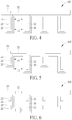
- FIGs. 1 ⁇ 6 are structural diagrams illustrating micro device transfer head arrays 101 ⁇ 106 according to embodiments of the present invention.
- Each of the micro device transfer head arrays 101 ⁇ 106 includes a plurality of transfer heads (only two transfer heads are depicted for illustrative purpose) for transferring a predetermined amount of micro devices to a substrate.
- Each transfer head includes a first side arm 10, a second side arm 20, a base arm 30, and an isolation layer 40.
- the first side arm 10 and the second side arm 20 are structures extending from both ends of the base arm 30, respectively.
- the space between the first side arm 10 and the second side arm 20 may provide room to clamp and accommodate a micro device.
- the isolation layer 40 covers the surface of the first side arm 10 and the second side arm 20, as well as covers one surface of the base arm 30.
- first end of first side arm 10 and the first end of the second side arm 20 are contact ends to the base arm 30, while the second end of first side arm 10 and the second end of the second side arm 20 are clamping ends.
- the distance between the first end of first side arm 10 and the first end of the second side arm 20 is represented by d1, while the distance between the second end of first side arm 10 and the second end of the second side arm 20 is represented by d2.
- the first side arm 10 includes one or multiple electrodes 12 and the second side arm 20 includes one or multiple electrodes 22.
- the first side arm 10 and the second side arm 20 are of the same length.
- the first side arm 10 is longer than the second side arm 20.
- the first side arm 10 and the second side arm 20 are of the same length and both include a hook-shaped second end.
- the first side arm 10 includes one or multiple electrodes 12, the second side arm 20 includes one or multiple electrodes 22, and the base arm 30 includes one or multiple electrodes 32.
- the first side arm 10 and the second side arm 20 are of the same length.
- the first side arm 10 is longer than the second side arm 20.
- the first side arm 10 and the second side arm 20 are of the same length and both include a hook-shaped second end.
- FIGs. 7 ⁇ 9 are structural diagrams illustrating micro device transfer head arrays 107 ⁇ 109 according to embodiments of the present invention.
- Each of the micro device transfer head arrays 107 ⁇ 109 includes a plurality of transfer heads (only two transfer heads are depicted for illustrative purpose) for transferring a predetermined amount of micro devices to a substrate.
- Each transfer head includes a first side arm 10, a second side arm 20, two base arms 31 and 35, and an isolation layer 40.
- the first side arm 10 and the second side arm 20 are structures extending from both ends of the base arm 31, respectively.
- the space between the first side arm 10 and the second side arm 20 may provide room to clamp and accommodate a micro device.
- the isolation layer 40 covers the surface of the first side arm 10 and the second side arm 20, as well as covers a first surface of the base arm 31.
- the base arm 35 is disposed on a second surface of the base arm 31.
- the space between the base arm 31 and the base arm 35 may provide deformation room for operating the micro device transfer head arrays 107-109, which will be illustrated in detail in subsequent paragraphs.
- the first end of first side arm 10 and the first end of the second side arm 20 are contact ends to the base arm 31, while the second end of first side arm 10 and the second end of the second side arm 20 are clamping ends.
- the distance between the first end of first side arm 10 and the first end of the second side arm 20 is represented by d1
- the distance between the second end of first side arm 10 and the second end of the second side arm 20 is represented by d2.
- the first side arm 10 includes one or multiple electrodes 12, the second side arm 20 includes one or multiple electrodes 22, the base arm 31 includes one or multiple electrodes 32, and the base arm 35 includes one or multiple sensing elements 42.
- the one or multiple sensing elements 42 may be one or multiple electrodes or electromagnetic coils.
- the first side arm 10 and the second side arm 20 are of the same length.
- the first side arm 10 is shorter than the second side arm 20.
- the micro device transfer head array 109 depicted in FIG. 9 the first side arm 10 and the second side arm 20 are of the same length and both include a hook-shaped second end.
- FIGs. 10 ⁇ 12 are structural diagrams illustrating micro device transfer head arrays 110 ⁇ 112 according to embodiments of the present invention.
- Each of the micro device transfer head arrays 110 ⁇ 112 includes a plurality of transfer heads (only two transfer heads are depicted for illustrative purpose) for transferring a predetermined amount of micro devices to a substrate.
- Each transfer head includes a first side arm 10, a second side arm 20, a base arm 30, an isolation layer 40, and adjusting arms 51 and 53.
- the first side arm 10 and the second side arm 20 are structures extending from both ends of the base arm 30, respectively. The space between the first side arm 10 and the second side arm 20 may provide room to clamp and accommodate a micro device.
- the isolation layer 40 covers the surface of the first side arm 10 and the second side arm 20, as well as covers a first surface of the base arm 30.
- the adjusting arms 51 and 53 are disposed on a second surface of the base arm 30, wherein the location of each adjusting arm 51 corresponds to the space between the first side arm 10 and the second side arm 20 in each transfer head, while the location of each adjusting arm 53 corresponds to the space between each transfer head.
- the first end of first side arm 10 and the first end of the second side arm 20 are contact ends to the base arm 30, while the second end of first side arm 10 and the second end of the second side arm 20 are clamping ends.
- the distance between the first end of first side arm 10 and the first end of the second side arm 20 is represented by d1
- the distance between the second end of first side arm 10 and the second end of the second side arm 20 is represented by d2.
- the first side arm 10 includes one or multiple electrodes 12, and the second side arm 20 includes one or multiple electrodes 22.
- the first side arm 10 and the second side arm 20 are of the same length.
- the first side arm 10 is longer than the second side arm 20.
- the first side arm 10 and the second side arm 20 are of the same length and both include a hook-shaped second end.
- FIGs. 13A ⁇ 13E are diagrams illustrating the operation of the micro device transfer head arrays 101 ⁇ 103 according to embodiments of the present invention.
- FIGs. 13A ⁇ 13E depict the 5-state operation of the micro device transfer head array 102.
- the electrodes 12 and 22 are not charged, and the distance between the first side arm 10 and its corresponding micro device 5 is h0.
- the electrodes 12 is charged, and the micro device transfer head array 102 is moved within the sensing range of the corresponding micro device 5 (as indicated by arrow S1), wherein the distance between the first side arm 10 and its corresponding micro device 5 is h1 (h1 ⁇ h0).
- the micro device transfer head array 102 is moved in the lateral direction (as indicated by arrow S2) so that the charged electrode 12 may draw the corresponding micro device 5 away from the substrate to move towards the space between the first side arm 10 and the second side arm 20(as indicated by arrow S3).
- the corresponding micro device 5 may be drawn into the space between the first side arm 10 and the second side arm 20(as indicated by arrow S4).
- the induced attraction force shortens the distance between the second end of the first side arm 10 and the second end of the second side arm 20 (d2>d1), thereby clamping the corresponding micro device 5 steadily.
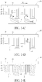
- FIGs. 14A ⁇ 14E are diagrams illustrating the operation of the micro device transfer head arrays 104 ⁇ 106 according to embodiments of the present invention.
- FIGs. 14A ⁇ 14E depict the 5-state operation of the micro device transfer head array 105.
- the electrodes 12 and 22 are not charged, and the distance between the first side arm 10 and its corresponding micro device 5 is h0.
- the electrodes 12 is charged, and the micro device transfer head array 105 is moved within the sensing range of the corresponding micro device 5 (as indicated by arrow S1), wherein the distance between the first side arm 10 and the corresponding micro device 5 is h1 (h1 ⁇ h0).
- the micro device transfer head array 105 is moved in the lateral direction (as indicated by arrow S2) so that the charged electrode 12 may draw the corresponding micro device 5 away from the substrate to move towards the space between the first side arm 10 and the second side arm 20(as indicated by arrow S3).
- the corresponding micro device 5 may be drawn into the space between the first side arm 10 and the second side arm 20. Meanwhile, the electrode 32 is charged to further draw the corresponding micro device 5 towards the base arm 30 to fully be accommodated inside the space between the first side arm 10 and the second side arm 20 (as indicated by arrow S4).
- the induced attraction force shortens the distance between the second end of the first side arm 10 and the second end of the second side arm 20 (d2>d1), thereby clamping the corresponding micro device 5 steadily.
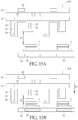
- FIGs. 15A ⁇ 15E are diagrams illustrating the operation of the micro device transfer head arrays 107 ⁇ 109 according to embodiments of the present invention.
- FIGs. 15A ⁇ 15E depict the 5-state operation of the micro device transfer head array 108 with an auxiliary board 50.
- the auxiliary board 50 includes one or multiple sensing elements 52 each associated with a corresponding micro device 5.
- the electrodes 12 and 22 are not charged, and the distance between the first side arm 10 and its corresponding micro device 5 is h0.
- the one or multiple sensing elements 52 of the auxiliary board 50 are aligned with corresponding one or multiple micro devices 5, but are not in contact with the substrate which contains the one or multiple micro devices 5.
- the auxiliary board 50 is moved towards the substrate which contains the one or multiple micro devices 5 and the one or multiple sensing elements 52 are charged, while the micro device transfer head array 108 is moved within the sensing range of the corresponding micro device 5 and the electrodes 12 is charged (as indicated by arrow S1), wherein the distance between the first side arm 10 and the corresponding micro device 5 is h1 (h1 ⁇ h0).
- the third state depicted in FIG. 15B the auxiliary board 50 is moved towards the substrate which contains the one or multiple micro devices 5 and the one or multiple sensing elements 52 are charged, while the micro device transfer head array 108 is moved within the sensing range of the corresponding micro device 5 and the electrodes 12 is charged (as indicated by arrow S1), wherein the distance between the first side arm 10 and the corresponding micro device 5 is h1 (h1 ⁇ h0).
- the micro device transfer head array 108 is moved in the lateral direction (as indicated by arrow S2) so that the charged electrode 12 may draw the corresponding micro device 5 away from the substrate to move towards the space between the first side arm 10 and the second side arm 20(as indicated by arrow S3).
- the corresponding micro device 5 may be drawn into the space between the first side arm 10 and the second side arm 20.
- the electrode 32 is charged to further draw the corresponding micro device 5 towards the base arm 30 to fully be accommodated inside the space between the first side arm 10 and the second side arm 20 (as indicated by arrow S4).
- the induced attraction force shortens the distance between the base arm 31 and the base arm 35 so that the base arm 31 encounters deformation which changes the relative locations of both ends of the first side arm 10 and the second side arm 20 (d2>d1), thereby clamping the corresponding micro device 5 steadily.
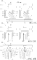
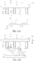
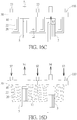
- FIGs. 16A ⁇ 16D are diagrams illustrating the operation of the micro device transfer head arrays 110 ⁇ 112 according to embodiments of the present invention.
- FIGs. 16A ⁇ 16D depict the 4-state operation of the micro device transfer head array 110 with an auxiliary board 60.
- the auxiliary board 60 includes one or multiple bulging structures 62 each associated with a corresponding micro device 5.
- the electrodes 12 and 22 are not charged, and the distance between the first side arm 10 and its corresponding micro device 5 is h0.
- An edge-cutting procedure is performed on the substrate containing the one or more micro devices, thereby weakening the edges which define the one or more micro devices.
- the one or multiple sensing elements 52 of the auxiliary board 50 are aligned with corresponding one or multiple micro devices 5, but are not in contact with the substrate which contains the one or multiple micro devices 5.
- the auxiliary board 50 is moved towards the substrate which contains the one or multiple micro devices 5 so that one end of the one or multiple micro devices 5 may be jacked up.
- the electrodes 12 is charged and the micro device transfer head array 110 is moved within the sensing range of the corresponding micro device 5(as indicated by arrow S1) until the corresponding micro device 5 may be drawn into the space between the first side arm 10 and the second side arm 20(as indicated by arrow S3).
- each adjusting arm 51 is applied with an upward force and each adjusting arm 53 is applied with an downward force so that the base arm 30 may encounter deformation which changes the relative locations of both ends of the first side arm 10 and the second side arm 20 (d2 ⁇ d1), thereby clamping the corresponding micro device 5 stably.
- the present invention provides a micro device transfer head array and a related method capable of mass-transferring micro LEDs rapidly and efficiently.
Landscapes
- Engineering & Computer Science (AREA)
- Manufacturing & Machinery (AREA)
- Microelectronics & Electronic Packaging (AREA)
- Container, Conveyance, Adherence, Positioning, Of Wafer (AREA)
- Robotics (AREA)
Abstract
Description
- The present invention is related to a micro device transfer head and a related method capable of mass-transferring micro LEDs rapidly and efficiently.
- Compared to traditional incandescent bulbs, light-emitting diodes (LEDs) are advantageous in low power consumption, long lifetime, small size, no warm-up time, fast reaction speed, and the ability to be manufactured as small or array devices. In addition to outdoor displays, traffic signs, and liquid crystal display (LCD) backlight for various electronic devices such as mobile phones, notebook computers or personal digital assistants (PDAs), LEDs are also widely used as indoor/outdoor lighting devices in place of fluorescent of incandescent lamps. An LED may adopt front-emission micro devices or side-emission micro devices. Front-emission micro devices provide wider viewing angles, but have poor performances in emission efficiency and half wavelength. Side-emission micro devices excel in high emission efficiency and better half wavelength, but can only provide narrower viewing angles.
- The size of traditional LED arrays is the dimension of millimeters (mm). The size of micro LED arrays may be reduced to the dimension of micrometers (µm) while inheriting the same good performances regarding power consumption, brightness, resolution, color saturation, reaction speed, life time and efficiency. In a micro LED manufacturing process, a thin-film, miniaturized and array design is adopted so that multiple micro LEDs are fabricated in the dimension of merely 1-250µm. Next, these micro LEDs are mass transferred to be disposed on another circuit board. Protection layers and upper electrodes may be formed in a physical deposition process before packaging the upper substrate.
- Therefore, there is a need for a micro device transfer head array and a related method capable of mass-transferring micro LEDs rapidly and efficiently.
- The present invention aims at providing a micro device transfer head and a related method capable of mass-transferring micro LEDs rapidly and efficiently.
- This is achieved by a micro device transfer head according to
claim 1 and a method of transferring a micro device using a micro device transfer head according to claim 7. The dependent claims pertain to corresponding further developments and improvements. - As will be seen more clearly from the detailed description following below, the claimed micro device transfer head includes a base arm, a first side arm, a second side arm and an isolation layer. The first base arm includes a first surface and a second surface. The first side arm includes one or multiple first electrodes and is disposed on the first surface of the base arm at a first end of the base arm. The second side arm includes one or multiple second electrodes and is disposed on the first surface of the base arm at a second end of the base arm. The isolation layer is disposed on the first surface of the base arm and covers a surface of the first side arm and a surface of the second side arm.
- As will be seen more clearly from the detailed description following below, the claimed method of transferring a micro device uses a micro device transfer head which includes a first base arm, a first side arm and a second side arm with the micro device fabricated on a substrate. The claimed method includes moving the first side arm within a sensing range of the micro device, charging the first side arm for drawing the micro device away from the substrate to move towards a space between the first side arm and the second side arm, and shortening a distance between the first side arm and the second side arm for clamping the micro device.
- In the following, the invention is further illustrated by way of example, taking reference to the accompanying drawings.
-
FIG. 1 is a structural diagram illustrating a micro device transfer head array according to an embodiment of the present invention. -
FIG. 2 is a structural diagram illustrating a micro device transfer head array according to another embodiment of the present invention. -
FIG. 3 is a structural diagram illustrating a micro device transfer head array according to another embodiment of the present invention. -
FIG. 4 is a structural diagram illustrating a micro device transfer head array according to another embodiment of the present invention. -
FIG. 5 is a structural diagram illustrating a micro device transfer head array according to another embodiment of the present invention. -
FIG. 6 is a structural diagram illustrating a micro device transfer head array according to another embodiment of the present invention. -
FIG. 7 is a structural diagram illustrating a micro device transfer head array according to another embodiment of the present invention. -
FIG. 8 is a structural diagram illustrating a micro device transfer head array according to another embodiment of the present invention. -
FIG. 9 is a structural diagram illustrating a micro device transfer head array according to another embodiment of the present invention. -
FIG. 10 is a structural diagram illustrating a micro device transfer head array according to another embodiment of the present invention. -
FIG. 11 is a structural diagram illustrating a micro device transfer head array according to another embodiment of the present invention. -
FIG. 12 is a structural diagram illustrating a micro device transfer head array according to another embodiment of the present invention. -
FIGs. 13A∼13E are diagrams illustrating the operation of a micro device transfer head array according to an embodiments of the present invention. -
FIGs. 14A∼14E are diagrams illustrating the operation of a micro device transfer head array according to another embodiments of the present invention. -
FIGs. 15A∼15E are diagrams illustrating the operation of a micro device transfer head array according to another embodiments of the present invention. -
FIGs. 16A∼16D are diagrams illustrating the operation of a micro device transfer head array according to another embodiment of the present invention. -
FIGs. 1∼6 are structural diagrams illustrating micro devicetransfer head arrays 101∼106 according to embodiments of the present invention. Each of the micro devicetransfer head arrays 101∼106 includes a plurality of transfer heads (only two transfer heads are depicted for illustrative purpose) for transferring a predetermined amount of micro devices to a substrate. Each transfer head includes afirst side arm 10, asecond side arm 20, abase arm 30, and anisolation layer 40. Thefirst side arm 10 and thesecond side arm 20 are structures extending from both ends of thebase arm 30, respectively. The space between thefirst side arm 10 and thesecond side arm 20 may provide room to clamp and accommodate a micro device. Theisolation layer 40 covers the surface of thefirst side arm 10 and thesecond side arm 20, as well as covers one surface of thebase arm 30. The first end offirst side arm 10 and the first end of thesecond side arm 20 are contact ends to thebase arm 30, while the second end offirst side arm 10 and the second end of thesecond side arm 20 are clamping ends. The distance between the first end offirst side arm 10 and the first end of thesecond side arm 20 is represented by d1, while the distance between the second end offirst side arm 10 and the second end of thesecond side arm 20 is represented by d2. - In the embodiments illustrated in
FIGs. 1-3 , thefirst side arm 10 includes one ormultiple electrodes 12 and thesecond side arm 20 includes one ormultiple electrodes 22. In the micro devicetransfer head array 101 depicted inFIG. 1 , thefirst side arm 10 and thesecond side arm 20 are of the same length. In the micro devicetransfer head array 102 depicted inFIG. 2 , thefirst side arm 10 is longer than thesecond side arm 20. In the micro devicetransfer head array 103 depicted inFIG. 3 , thefirst side arm 10 and thesecond side arm 20 are of the same length and both include a hook-shaped second end. - In the embodiments illustrated in
FIGs. 4-6 , thefirst side arm 10 includes one ormultiple electrodes 12, thesecond side arm 20 includes one ormultiple electrodes 22, and thebase arm 30 includes one ormultiple electrodes 32. In the micro devicetransfer head array 104 depicted inFIG. 4 , thefirst side arm 10 and thesecond side arm 20 are of the same length. In the micro devicetransfer head array 105 depicted inFIG. 5 , thefirst side arm 10 is longer than thesecond side arm 20. In the micro devicetransfer head array 106 depicted inFIG. 6 , thefirst side arm 10 and thesecond side arm 20 are of the same length and both include a hook-shaped second end. -
FIGs. 7∼9 are structural diagrams illustrating micro devicetransfer head arrays 107∼109 according to embodiments of the present invention. Each of the micro devicetransfer head arrays 107∼109 includes a plurality of transfer heads (only two transfer heads are depicted for illustrative purpose) for transferring a predetermined amount of micro devices to a substrate. Each transfer head includes afirst side arm 10, asecond side arm 20, twobase arms isolation layer 40. Thefirst side arm 10 and thesecond side arm 20 are structures extending from both ends of thebase arm 31, respectively. The space between thefirst side arm 10 and thesecond side arm 20 may provide room to clamp and accommodate a micro device. Theisolation layer 40 covers the surface of thefirst side arm 10 and thesecond side arm 20, as well as covers a first surface of thebase arm 31. Thebase arm 35 is disposed on a second surface of thebase arm 31. The space between thebase arm 31 and thebase arm 35 may provide deformation room for operating the micro device transfer head arrays 107-109, which will be illustrated in detail in subsequent paragraphs. The first end offirst side arm 10 and the first end of thesecond side arm 20 are contact ends to thebase arm 31, while the second end offirst side arm 10 and the second end of thesecond side arm 20 are clamping ends. The distance between the first end offirst side arm 10 and the first end of thesecond side arm 20 is represented by d1, while the distance between the second end offirst side arm 10 and the second end of thesecond side arm 20 is represented by d2. - In the embodiments illustrated in
FIGs. 7-9 , thefirst side arm 10 includes one ormultiple electrodes 12, thesecond side arm 20 includes one ormultiple electrodes 22, thebase arm 31 includes one ormultiple electrodes 32, and thebase arm 35 includes one ormultiple sensing elements 42. The one ormultiple sensing elements 42 may be one or multiple electrodes or electromagnetic coils. In the micro devicetransfer head array 107 depicted inFIG. 7 , thefirst side arm 10 and thesecond side arm 20 are of the same length. In the micro devicetransfer head array 108 depicted inFIG. 8 , thefirst side arm 10 is shorter than thesecond side arm 20. In the micro devicetransfer head array 109 depicted inFIG. 9 , thefirst side arm 10 and thesecond side arm 20 are of the same length and both include a hook-shaped second end. -
FIGs. 10∼12 are structural diagrams illustrating micro devicetransfer head arrays 110∼112 according to embodiments of the present invention. Each of the micro devicetransfer head arrays 110∼112 includes a plurality of transfer heads (only two transfer heads are depicted for illustrative purpose) for transferring a predetermined amount of micro devices to a substrate. Each transfer head includes afirst side arm 10, asecond side arm 20, abase arm 30, anisolation layer 40, and adjustingarms first side arm 10 and thesecond side arm 20 are structures extending from both ends of thebase arm 30, respectively. The space between thefirst side arm 10 and thesecond side arm 20 may provide room to clamp and accommodate a micro device. Theisolation layer 40 covers the surface of thefirst side arm 10 and thesecond side arm 20, as well as covers a first surface of thebase arm 30. The adjustingarms base arm 30, wherein the location of each adjustingarm 51 corresponds to the space between thefirst side arm 10 and thesecond side arm 20 in each transfer head, while the location of each adjustingarm 53 corresponds to the space between each transfer head. The first end offirst side arm 10 and the first end of thesecond side arm 20 are contact ends to thebase arm 30, while the second end offirst side arm 10 and the second end of thesecond side arm 20 are clamping ends. The distance between the first end offirst side arm 10 and the first end of thesecond side arm 20 is represented by d1, while the distance between the second end offirst side arm 10 and the second end of thesecond side arm 20 is represented by d2. - In the embodiments illustrated in
FIGs. 10-12 , thefirst side arm 10 includes one ormultiple electrodes 12, and thesecond side arm 20 includes one ormultiple electrodes 22. In the micro devicetransfer head array 110 depicted in FIG. 110, thefirst side arm 10 and thesecond side arm 20 are of the same length. In the micro devicetransfer head array 111 depicted inFIG. 11 , thefirst side arm 10 is longer than thesecond side arm 20. In the micro devicetransfer head array 112 depicted inFIG. 12 , thefirst side arm 10 and thesecond side arm 20 are of the same length and both include a hook-shaped second end. -
FIGs. 13A∼13E are diagrams illustrating the operation of the micro devicetransfer head arrays 101∼103 according to embodiments of the present invention. For illustrative purpose,FIGs. 13A∼13E depict the 5-state operation of the micro devicetransfer head array 102. In the initial first state depicted inFIG. 13A , theelectrodes first side arm 10 and its correspondingmicro device 5 is h0. In the second state depicted inFIG. 13B , theelectrodes 12 is charged, and the micro devicetransfer head array 102 is moved within the sensing range of the corresponding micro device 5 (as indicated by arrow S1), wherein the distance between thefirst side arm 10 and its correspondingmicro device 5 is h1 (h1<h0). In the third state depicted inFIG. 13C , the micro devicetransfer head array 102 is moved in the lateral direction (as indicated by arrow S2) so that the chargedelectrode 12 may draw the correspondingmicro device 5 away from the substrate to move towards the space between thefirst side arm 10 and the second side arm 20(as indicated by arrow S3). In the fourth state depicted inFIG. 13D , with the lateral movement of the micro devicetransfer head array 102 and under the attraction force induced by the chargedelectrode 12, the correspondingmicro device 5 may be drawn into the space between thefirst side arm 10 and the second side arm 20(as indicated by arrow S4). In the fifth state depicted inFIG. 13E , when theelectrodes first side arm 10 and the second end of the second side arm 20 (d2>d1), thereby clamping the correspondingmicro device 5 steadily. -
FIGs. 14A∼14E are diagrams illustrating the operation of the micro devicetransfer head arrays 104∼106 according to embodiments of the present invention. For illustrative purpose,FIGs. 14A∼14E depict the 5-state operation of the micro devicetransfer head array 105. In the initial first state depicted inFIG. 14A , theelectrodes first side arm 10 and its correspondingmicro device 5 is h0. In the second state depicted inFIG. 14B , theelectrodes 12 is charged, and the micro devicetransfer head array 105 is moved within the sensing range of the corresponding micro device 5 (as indicated by arrow S1), wherein the distance between thefirst side arm 10 and the correspondingmicro device 5 is h1 (h1<h0). In the third state depicted inFIG. 14C , the micro devicetransfer head array 105 is moved in the lateral direction (as indicated by arrow S2) so that the chargedelectrode 12 may draw the correspondingmicro device 5 away from the substrate to move towards the space between thefirst side arm 10 and the second side arm 20(as indicated by arrow S3). In the fourth state depicted inFIG. 14D , with the lateral movement of the micro devicetransfer head array 105 and under the attraction force induced by the chargedelectrode 12, the correspondingmicro device 5 may be drawn into the space between thefirst side arm 10 and thesecond side arm 20. Meanwhile, theelectrode 32 is charged to further draw the correspondingmicro device 5 towards thebase arm 30 to fully be accommodated inside the space between thefirst side arm 10 and the second side arm 20 (as indicated by arrow S4). In the fifth state depicted inFIG. 14E , when theelectrodes first side arm 10 and the second end of the second side arm 20 (d2>d1), thereby clamping the correspondingmicro device 5 steadily. -
FIGs. 15A∼15E are diagrams illustrating the operation of the micro devicetransfer head arrays 107∼109 according to embodiments of the present invention. For illustrative purpose,FIGs. 15A∼15E depict the 5-state operation of the micro devicetransfer head array 108 with anauxiliary board 50. Theauxiliary board 50 includes one ormultiple sensing elements 52 each associated with a correspondingmicro device 5. In the initial first state depicted inFIG. 15A , theelectrodes first side arm 10 and its correspondingmicro device 5 is h0. Under such circumstance, the one ormultiple sensing elements 52 of theauxiliary board 50 are aligned with corresponding one or multiplemicro devices 5, but are not in contact with the substrate which contains the one or multiplemicro devices 5. In the second state depicted inFIG. 15B , theauxiliary board 50 is moved towards the substrate which contains the one or multiplemicro devices 5 and the one ormultiple sensing elements 52 are charged, while the micro devicetransfer head array 108 is moved within the sensing range of the correspondingmicro device 5 and theelectrodes 12 is charged (as indicated by arrow S1), wherein the distance between thefirst side arm 10 and the correspondingmicro device 5 is h1 (h1<h0). In the third state depicted inFIG. 15C , the micro devicetransfer head array 108 is moved in the lateral direction (as indicated by arrow S2) so that the chargedelectrode 12 may draw the correspondingmicro device 5 away from the substrate to move towards the space between thefirst side arm 10 and the second side arm 20(as indicated by arrow S3). In the fourth state depicted inFIG. 15D , with the lateral movement of the micro devicetransfer head array 108 and under the attraction force induced by the chargedelectrode 12, the correspondingmicro device 5 may be drawn into the space between thefirst side arm 10 and thesecond side arm 20. Meanwhile, theelectrode 32 is charged to further draw the correspondingmicro device 5 towards thebase arm 30 to fully be accommodated inside the space between thefirst side arm 10 and the second side arm 20 (as indicated by arrow S4). In the fifth state depicted inFIG. 15E , when thesensing element 42 and theelectrode 12 are then charged by voltages of opposite polarities, the induced attraction force shortens the distance between thebase arm 31 and thebase arm 35 so that thebase arm 31 encounters deformation which changes the relative locations of both ends of thefirst side arm 10 and the second side arm 20 (d2>d1), thereby clamping the correspondingmicro device 5 steadily. -
FIGs. 16A∼16D are diagrams illustrating the operation of the micro devicetransfer head arrays 110∼112 according to embodiments of the present invention. For illustrative purpose,FIGs. 16A∼16D depict the 4-state operation of the micro devicetransfer head array 110 with anauxiliary board 60. Theauxiliary board 60 includes one or multiple bulgingstructures 62 each associated with a correspondingmicro device 5. In the initial first state depicted inFIG. 16A , theelectrodes first side arm 10 and its correspondingmicro device 5 is h0. An edge-cutting procedure is performed on the substrate containing the one or more micro devices, thereby weakening the edges which define the one or more micro devices. The one ormultiple sensing elements 52 of theauxiliary board 50 are aligned with corresponding one or multiplemicro devices 5, but are not in contact with the substrate which contains the one or multiplemicro devices 5. In the second state depicted inFIG. 15B , theauxiliary board 50 is moved towards the substrate which contains the one or multiplemicro devices 5 so that one end of the one or multiplemicro devices 5 may be jacked up. Meanwhile, theelectrodes 12 is charged and the micro devicetransfer head array 110 is moved within the sensing range of the corresponding micro device 5(as indicated by arrow S1) until the correspondingmicro device 5 may be drawn into the space between thefirst side arm 10 and the second side arm 20(as indicated by arrow S3). In the fourth state depicted inFIG. 16D , each adjustingarm 51 is applied with an upward force and each adjustingarm 53 is applied with an downward force so that thebase arm 30 may encounter deformation which changes the relative locations of both ends of thefirst side arm 10 and the second side arm 20 (d2<d1), thereby clamping the correspondingmicro device 5 stably. - In conclusion, the present invention provides a micro device transfer head array and a related method capable of mass-transferring micro LEDs rapidly and efficiently.
Claims (15)
- A micro device transfer head (101∼112), comprising:a first base arm (30, 31) including a first surface and a second surface;characterized by:a first side arm (10) including one or multiple first electrodes (12) and disposed on the first surface of the first base arm (30, 31) at a first end of the first base arm (30, 31);a second side arm (20) including one or multiple second electrodes (22) and disposed on the first surface of the first base arm (30, 31) at a second end of the first base arm (30, 31); andan isolation layer (40) disposed on the first surface of the first base arm (30, 31) and covering a surface of the first side arm (10) and a surface of the second side arm (20).
- The micro device transfer head (104∼109) of claim 1, characterized in that the first base arm (30, 31) further includes one or multiple third electrodes (32).
- The micro device transfer head (107∼109) of any of claim 1-2, further characterized by comprising:a second base arm (35) disposed on the second surface of the first base arm (31) and including one or multiple sensing elements (42).
- The micro device transfer head (107∼109) of claim 3, characterized in that the one or multiple sensing elements (42) are one or multiple electrodes or electromagnetic coils.
- The micro device transfer head (110∼112) of claim 1, further characterized by comprising:a first adjusting arm (51) disposed on the second surface of the first base arm (30) at a location corresponding to a space between the first side arm (10) and the second side arm (20);a second adjusting arm (53) disposed on the second surface of the first base arm (30) at the first end of the first base arm (30); anda third adjusting arm (53) disposed on the second surface of the first base arm (30) at the second end of the first base arm (30).
- The micro device transfer head (103, 106, 109, 112) of claim 1, characterized in that:the first side arm (10) includes a first hook-shaped structure at an end which is farthest away from the first base arm (30, 31); andthe second side arm (20) includes a second hook-shaped structure at an end which is farthest away from the first base arm (30, 31).
- A method of transferring a micro device (5) using a micro device transfer head (101∼112), wherein the micro device transfer head (101∼112) includes a first base arm (30, 31), a first side arm (10) and a second side arm (20), and the micro device (5) is fabricated on a substrate, the method characterized by comprising:moving the first side arm (10) within a sensing range of the micro device (5);charging the first side arm (10) for drawing the micro device (5) away from the substrate to move towards a space between the first side arm (10) and the second side arm (20); andshortening a distance between the first side arm (10) and the second side arm (20) for clamping the micro device (5).
- The method of claim 7, further characterized by comprising:charging the first base arm (30, 31) for drawing the micro device (5) into the space between the first side arm (10) and the second side arm (20) after charging the first side arm (10) for drawing the micro device (5) to move towards the space between the first side arm (10) and the second side arm (20).
- The method of claim 8, further characterized by comprising:applying a voltage of a first polarity to the first side arm (10) and applying a voltage of a second polarity to the second side arm (20) for shortening the distance between the first side arm (10) and the second side arm (20) after drawing the micro device (5) into the space between the first side arm (10) and the second side arm (20).
- The method of claim 8, wherein the micro transfer head (107∼109) further includes a second base arm (35), further characterized by comprising:applying a torque deformation on the first base arm (30) using the second base arm (35) for shortening the distance between the first side arm (10) and the second side arm (20).
- The method of claim 7, further characterized by comprising:moving the micro device transfer head (101∼112) along a predetermined direction so that the charged first side arm (10) draws the micro device (5) into the space between the first side arm (10) and the second side arm (20) after charging the first side arm (10) for drawing the micro device (5) to move towards the space between the first side arm (10) and the second side arm (20), wherein the predetermined direction is parallel to a surface of the substrate.
- The method of claim 11, further characterized by comprising:applying a voltage of a first polarity to the first side arm (10) and applying a voltage of a second polarity to the second side arm (20) for shortening the distance between the first side arm (10) and the second side arm (20) after drawing the micro device (5) into the space between the first side arm (10) and the second side arm (20).
- The method of claim 11, wherein the micro transfer head (107∼109) further includes a second base arm (35), characterized in that comprising:applying a torque deformation on the first base arm (30) using the second base arm (35) for shortening the distance between the first side arm (10) and the second side arm (20).
- The method of claim 7, further characterized by comprising:applying a first voltage to the substrate and applying a second voltage to the first side arm (10) so as to detach the micro device (5) from the substrate and move towards the space between the first side arm (10) and the second side arm (20), wherein the first voltage and the second voltage have opposite polarities.
- The method of claim 7, further characterized by comprising:performing an edge-cutting procedure on the substrate for defining a range of the micro device (5);jacking up an end of the micro device (5) away from the substrate using an auxiliary board (60); andcharging the first side arm (10) for detaching the micro device (5) from the substrate to move towards the space between the first side arm (10) and the second side arm (20).
Applications Claiming Priority (1)
| Application Number | Priority Date | Filing Date | Title |
|---|---|---|---|
| TW106146464A TWI635785B (en) | 2017-12-29 | 2017-12-29 | Micro component transfer head |
Publications (2)
| Publication Number | Publication Date |
|---|---|
| EP3506339A1 true EP3506339A1 (en) | 2019-07-03 |
| EP3506339B1 EP3506339B1 (en) | 2021-09-22 |
Family
ID=61906583
Family Applications (1)
| Application Number | Title | Priority Date | Filing Date |
|---|---|---|---|
| EP18162804.1A Not-in-force EP3506339B1 (en) | 2017-12-29 | 2018-03-20 | Micro device transfer head and related method |
Country Status (3)
| Country | Link |
|---|---|
| US (2) | US11004721B2 (en) |
| EP (1) | EP3506339B1 (en) |
| TW (1) | TWI635785B (en) |
Families Citing this family (7)
| Publication number | Priority date | Publication date | Assignee | Title |
|---|---|---|---|---|
| US10446728B2 (en) * | 2014-10-31 | 2019-10-15 | eLux, Inc. | Pick-and remove system and method for emissive display repair |
| CN111799205B (en) * | 2019-04-08 | 2024-02-09 | 群创光电股份有限公司 | Method for manufacturing electronic device |
| CN117766453A (en) * | 2019-04-08 | 2024-03-26 | 群创光电股份有限公司 | Transfer joints and methods of making electronic devices |
| US11670531B2 (en) | 2019-04-25 | 2023-06-06 | Meta Platforms Technologies, Llc | Bridge pick-up head for transferring semiconductor devices |
| US11756810B1 (en) * | 2019-12-27 | 2023-09-12 | Meta Platforms Technologies, Llc | Detection of force applied by pick-up tool for transferring semiconductor devices |
| CN112967949B (en) * | 2020-08-11 | 2022-05-20 | 重庆康佳光电技术研究院有限公司 | Transfer member, transfer device and transfer method |
| US12142510B2 (en) * | 2020-12-23 | 2024-11-12 | Intel Corporation | Carrier for microelectronic assemblies having direct bonding |
Citations (2)
| Publication number | Priority date | Publication date | Assignee | Title |
|---|---|---|---|---|
| US20140064904A1 (en) * | 2012-09-06 | 2014-03-06 | Andreas Bibl | Compliant micro device transfer head with integrated electrode leads |
| US20170054390A1 (en) * | 2015-08-17 | 2017-02-23 | Mikro Mesa Technology Co., Ltd. | Transfer head array |
Family Cites Families (7)
| Publication number | Priority date | Publication date | Assignee | Title |
|---|---|---|---|---|
| AU2003279763A1 (en) * | 2002-10-01 | 2004-04-23 | Microfabrica Inc. | Monolithic structures including alignment and/or retention fixtures for accepting components |
| US8415771B1 (en) * | 2012-05-25 | 2013-04-09 | LuxVue Technology Corporation | Micro device transfer head with silicon electrode |
| US8569115B1 (en) | 2012-07-06 | 2013-10-29 | LuxVue Technology Corporation | Method of forming a compliant bipolar micro device transfer head with silicon electrodes |
| US9391042B2 (en) * | 2012-12-14 | 2016-07-12 | Apple Inc. | Micro device transfer system with pivot mount |
| US9314930B2 (en) * | 2012-12-14 | 2016-04-19 | LuxVue Technology Corporation | Micro pick up array with integrated pivot mount |
| CN107039298B (en) * | 2016-11-04 | 2019-12-24 | 厦门市三安光电科技有限公司 | Micro-component transfer device, transfer method, manufacturing method, device and electronic device |
| CN106601661B (en) | 2017-01-09 | 2019-08-27 | 京东方科技集团股份有限公司 | Transfer device and transfer method |
-
2017
- 2017-12-29 TW TW106146464A patent/TWI635785B/en active
-
2018
- 2018-03-13 US US15/919,235 patent/US11004721B2/en active Active
- 2018-03-20 EP EP18162804.1A patent/EP3506339B1/en not_active Not-in-force
-
2021
- 2021-04-05 US US17/222,944 patent/US11495485B2/en active Active
Patent Citations (2)
| Publication number | Priority date | Publication date | Assignee | Title |
|---|---|---|---|---|
| US20140064904A1 (en) * | 2012-09-06 | 2014-03-06 | Andreas Bibl | Compliant micro device transfer head with integrated electrode leads |
| US20170054390A1 (en) * | 2015-08-17 | 2017-02-23 | Mikro Mesa Technology Co., Ltd. | Transfer head array |
Also Published As
| Publication number | Publication date |
|---|---|
| TWI635785B (en) | 2018-09-11 |
| US20190206714A1 (en) | 2019-07-04 |
| TW201931987A (en) | 2019-08-01 |
| US20210225686A1 (en) | 2021-07-22 |
| US11495485B2 (en) | 2022-11-08 |
| US11004721B2 (en) | 2021-05-11 |
| EP3506339B1 (en) | 2021-09-22 |
Similar Documents
| Publication | Publication Date | Title |
|---|---|---|
| US11495485B2 (en) | Method of transferring micro device using micro device transfer head | |
| KR102784204B1 (en) | Method for manufacturing display device and substrate for manufacturing display device | |
| KR102906782B1 (en) | Display device using micro led and manufacturing method thereof | |
| US20190244846A1 (en) | Transfer device | |
| KR102011179B1 (en) | Smart pixel lighting and display microcontroller | |
| KR20190126260A (en) | Display device using micro led and manufacturing method thereof | |
| KR20190105537A (en) | Display device using micro led and manufacturing method thereof | |
| US12249524B2 (en) | Transfer structure and manufacturing method thereof, transfer device and manufacturing method thereof | |
| KR20190121274A (en) | Display device using micro led and manufacturing method thereof | |
| KR20190143840A (en) | Display device related to micro led and manufacturing method thereof | |
| KR20190104276A (en) | Display device using micro led and manufacturing method thereof | |
| KR102794952B1 (en) | Method for manufacturing display device and substrate for manufacturing display device | |
| US20250248170A1 (en) | Manufacturing method of display device | |
| CN104654135A (en) | Light source module and backlight module and liquid crystal display with light source module | |
| EP3509094A1 (en) | Micro device transfer equipment and related method | |
| US20250046772A1 (en) | Substrate structure for transcription of semiconductor light emitting device for pixel, and display device comprising same | |
| CN110062573B (en) | Micro component transfer head | |
| KR102957994B1 (en) | Manufacturing device for display devices | |
| KR102931254B1 (en) | Display device including semiconductor light emitting device | |
| KR102930043B1 (en) | Substrate for transferring semiconductor light-emitting devices for display pixels and display devices including the same | |
| KR102931255B1 (en) | An assembly substrate for transferring semiconductor light-emitting devices, a panel board onto which semiconductor light-emitting devices are transferred, and a display device including the same | |
| KR102916095B1 (en) | Transfer substrate including a semiconductor light-emitting device and method for transferring a semiconductor light emitting device | |
| CN102809813A (en) | Display device | |
| KR102698079B1 (en) | A Substrate structure for transferring semiconductor light emitting devices for pixels and Display device including the same | |
| KR20250171663A (en) | A transfer device for semiconductor light emitting devices for display pixels |
Legal Events
| Date | Code | Title | Description |
|---|---|---|---|
| PUAI | Public reference made under article 153(3) epc to a published international application that has entered the european phase |
Free format text: ORIGINAL CODE: 0009012 |
|
| STAA | Information on the status of an ep patent application or granted ep patent |
Free format text: STATUS: THE APPLICATION HAS BEEN PUBLISHED |
|
| AK | Designated contracting states |
Kind code of ref document: A1 Designated state(s): AL AT BE BG CH CY CZ DE DK EE ES FI FR GB GR HR HU IE IS IT LI LT LU LV MC MK MT NL NO PL PT RO RS SE SI SK SM TR |
|
| AX | Request for extension of the european patent |
Extension state: BA ME |
|
| STAA | Information on the status of an ep patent application or granted ep patent |
Free format text: STATUS: REQUEST FOR EXAMINATION WAS MADE |
|
| 17P | Request for examination filed |
Effective date: 20190715 |
|
| RBV | Designated contracting states (corrected) |
Designated state(s): AL AT BE BG CH CY CZ DE DK EE ES FI FR GB GR HR HU IE IS IT LI LT LU LV MC MK MT NL NO PL PT RO RS SE SI SK SM TR |
|
| GRAP | Despatch of communication of intention to grant a patent |
Free format text: ORIGINAL CODE: EPIDOSNIGR1 |
|
| STAA | Information on the status of an ep patent application or granted ep patent |
Free format text: STATUS: GRANT OF PATENT IS INTENDED |
|
| INTG | Intention to grant announced |
Effective date: 20210517 |
|
| GRAS | Grant fee paid |
Free format text: ORIGINAL CODE: EPIDOSNIGR3 |
|
| GRAA | (expected) grant |
Free format text: ORIGINAL CODE: 0009210 |
|
| STAA | Information on the status of an ep patent application or granted ep patent |
Free format text: STATUS: THE PATENT HAS BEEN GRANTED |
|
| AK | Designated contracting states |
Kind code of ref document: B1 Designated state(s): AL AT BE BG CH CY CZ DE DK EE ES FI FR GB GR HR HU IE IS IT LI LT LU LV MC MK MT NL NO PL PT RO RS SE SI SK SM TR |
|
| REG | Reference to a national code |
Ref country code: GB Ref legal event code: FG4D |
|
| REG | Reference to a national code |
Ref country code: DE Ref legal event code: R096 Ref document number: 602018023802 Country of ref document: DE |
|
| REG | Reference to a national code |
Ref country code: IE Ref legal event code: FG4D |
|
| REG | Reference to a national code |
Ref country code: CH Ref legal event code: EP Ref country code: AT Ref legal event code: REF Ref document number: 1432968 Country of ref document: AT Kind code of ref document: T Effective date: 20211015 |
|
| REG | Reference to a national code |
Ref country code: LT Ref legal event code: MG9D |
|
| REG | Reference to a national code |
Ref country code: NL Ref legal event code: MP Effective date: 20210922 |
|
| PG25 | Lapsed in a contracting state [announced via postgrant information from national office to epo] |
Ref country code: LT Free format text: LAPSE BECAUSE OF FAILURE TO SUBMIT A TRANSLATION OF THE DESCRIPTION OR TO PAY THE FEE WITHIN THE PRESCRIBED TIME-LIMIT Effective date: 20210922 Ref country code: BG Free format text: LAPSE BECAUSE OF FAILURE TO SUBMIT A TRANSLATION OF THE DESCRIPTION OR TO PAY THE FEE WITHIN THE PRESCRIBED TIME-LIMIT Effective date: 20211222 Ref country code: NO Free format text: LAPSE BECAUSE OF FAILURE TO SUBMIT A TRANSLATION OF THE DESCRIPTION OR TO PAY THE FEE WITHIN THE PRESCRIBED TIME-LIMIT Effective date: 20211222 Ref country code: HR Free format text: LAPSE BECAUSE OF FAILURE TO SUBMIT A TRANSLATION OF THE DESCRIPTION OR TO PAY THE FEE WITHIN THE PRESCRIBED TIME-LIMIT Effective date: 20210922 Ref country code: FI Free format text: LAPSE BECAUSE OF FAILURE TO SUBMIT A TRANSLATION OF THE DESCRIPTION OR TO PAY THE FEE WITHIN THE PRESCRIBED TIME-LIMIT Effective date: 20210922 Ref country code: RS Free format text: LAPSE BECAUSE OF FAILURE TO SUBMIT A TRANSLATION OF THE DESCRIPTION OR TO PAY THE FEE WITHIN THE PRESCRIBED TIME-LIMIT Effective date: 20210922 Ref country code: SE Free format text: LAPSE BECAUSE OF FAILURE TO SUBMIT A TRANSLATION OF THE DESCRIPTION OR TO PAY THE FEE WITHIN THE PRESCRIBED TIME-LIMIT Effective date: 20210922 |
|
| REG | Reference to a national code |
Ref country code: AT Ref legal event code: MK05 Ref document number: 1432968 Country of ref document: AT Kind code of ref document: T Effective date: 20210922 |
|
| PG25 | Lapsed in a contracting state [announced via postgrant information from national office to epo] |
Ref country code: LV Free format text: LAPSE BECAUSE OF FAILURE TO SUBMIT A TRANSLATION OF THE DESCRIPTION OR TO PAY THE FEE WITHIN THE PRESCRIBED TIME-LIMIT Effective date: 20210922 Ref country code: GR Free format text: LAPSE BECAUSE OF FAILURE TO SUBMIT A TRANSLATION OF THE DESCRIPTION OR TO PAY THE FEE WITHIN THE PRESCRIBED TIME-LIMIT Effective date: 20211223 |
|
| PG25 | Lapsed in a contracting state [announced via postgrant information from national office to epo] |
Ref country code: AT Free format text: LAPSE BECAUSE OF FAILURE TO SUBMIT A TRANSLATION OF THE DESCRIPTION OR TO PAY THE FEE WITHIN THE PRESCRIBED TIME-LIMIT Effective date: 20210922 |
|
| PG25 | Lapsed in a contracting state [announced via postgrant information from national office to epo] |
Ref country code: IS Free format text: LAPSE BECAUSE OF FAILURE TO SUBMIT A TRANSLATION OF THE DESCRIPTION OR TO PAY THE FEE WITHIN THE PRESCRIBED TIME-LIMIT Effective date: 20220122 Ref country code: SK Free format text: LAPSE BECAUSE OF FAILURE TO SUBMIT A TRANSLATION OF THE DESCRIPTION OR TO PAY THE FEE WITHIN THE PRESCRIBED TIME-LIMIT Effective date: 20210922 Ref country code: RO Free format text: LAPSE BECAUSE OF FAILURE TO SUBMIT A TRANSLATION OF THE DESCRIPTION OR TO PAY THE FEE WITHIN THE PRESCRIBED TIME-LIMIT Effective date: 20210922 Ref country code: PT Free format text: LAPSE BECAUSE OF FAILURE TO SUBMIT A TRANSLATION OF THE DESCRIPTION OR TO PAY THE FEE WITHIN THE PRESCRIBED TIME-LIMIT Effective date: 20220124 Ref country code: PL Free format text: LAPSE BECAUSE OF FAILURE TO SUBMIT A TRANSLATION OF THE DESCRIPTION OR TO PAY THE FEE WITHIN THE PRESCRIBED TIME-LIMIT Effective date: 20210922 Ref country code: NL Free format text: LAPSE BECAUSE OF FAILURE TO SUBMIT A TRANSLATION OF THE DESCRIPTION OR TO PAY THE FEE WITHIN THE PRESCRIBED TIME-LIMIT Effective date: 20210922 Ref country code: ES Free format text: LAPSE BECAUSE OF FAILURE TO SUBMIT A TRANSLATION OF THE DESCRIPTION OR TO PAY THE FEE WITHIN THE PRESCRIBED TIME-LIMIT Effective date: 20210922 Ref country code: EE Free format text: LAPSE BECAUSE OF FAILURE TO SUBMIT A TRANSLATION OF THE DESCRIPTION OR TO PAY THE FEE WITHIN THE PRESCRIBED TIME-LIMIT Effective date: 20210922 Ref country code: CZ Free format text: LAPSE BECAUSE OF FAILURE TO SUBMIT A TRANSLATION OF THE DESCRIPTION OR TO PAY THE FEE WITHIN THE PRESCRIBED TIME-LIMIT Effective date: 20210922 Ref country code: AL Free format text: LAPSE BECAUSE OF FAILURE TO SUBMIT A TRANSLATION OF THE DESCRIPTION OR TO PAY THE FEE WITHIN THE PRESCRIBED TIME-LIMIT Effective date: 20210922 |
|
| REG | Reference to a national code |
Ref country code: DE Ref legal event code: R097 Ref document number: 602018023802 Country of ref document: DE |
|
| PG25 | Lapsed in a contracting state [announced via postgrant information from national office to epo] |
Ref country code: DK Free format text: LAPSE BECAUSE OF FAILURE TO SUBMIT A TRANSLATION OF THE DESCRIPTION OR TO PAY THE FEE WITHIN THE PRESCRIBED TIME-LIMIT Effective date: 20210922 |
|
| PLBE | No opposition filed within time limit |
Free format text: ORIGINAL CODE: 0009261 |
|
| STAA | Information on the status of an ep patent application or granted ep patent |
Free format text: STATUS: NO OPPOSITION FILED WITHIN TIME LIMIT |
|
| 26N | No opposition filed |
Effective date: 20220623 |
|
| PG25 | Lapsed in a contracting state [announced via postgrant information from national office to epo] |
Ref country code: MC Free format text: LAPSE BECAUSE OF FAILURE TO SUBMIT A TRANSLATION OF THE DESCRIPTION OR TO PAY THE FEE WITHIN THE PRESCRIBED TIME-LIMIT Effective date: 20210922 |
|
| REG | Reference to a national code |
Ref country code: CH Ref legal event code: PL |
|
| PG25 | Lapsed in a contracting state [announced via postgrant information from national office to epo] |
Ref country code: SI Free format text: LAPSE BECAUSE OF FAILURE TO SUBMIT A TRANSLATION OF THE DESCRIPTION OR TO PAY THE FEE WITHIN THE PRESCRIBED TIME-LIMIT Effective date: 20210922 |
|
| REG | Reference to a national code |
Ref country code: BE Ref legal event code: MM Effective date: 20220331 |
|
| PG25 | Lapsed in a contracting state [announced via postgrant information from national office to epo] |
Ref country code: LU Free format text: LAPSE BECAUSE OF NON-PAYMENT OF DUE FEES Effective date: 20220320 Ref country code: LI Free format text: LAPSE BECAUSE OF NON-PAYMENT OF DUE FEES Effective date: 20220331 Ref country code: IT Free format text: LAPSE BECAUSE OF FAILURE TO SUBMIT A TRANSLATION OF THE DESCRIPTION OR TO PAY THE FEE WITHIN THE PRESCRIBED TIME-LIMIT Effective date: 20210922 Ref country code: IE Free format text: LAPSE BECAUSE OF NON-PAYMENT OF DUE FEES Effective date: 20220320 Ref country code: CH Free format text: LAPSE BECAUSE OF NON-PAYMENT OF DUE FEES Effective date: 20220331 |
|
| PG25 | Lapsed in a contracting state [announced via postgrant information from national office to epo] |
Ref country code: BE Free format text: LAPSE BECAUSE OF NON-PAYMENT OF DUE FEES Effective date: 20220331 |
|
| PG25 | Lapsed in a contracting state [announced via postgrant information from national office to epo] |
Ref country code: HU Free format text: LAPSE BECAUSE OF FAILURE TO SUBMIT A TRANSLATION OF THE DESCRIPTION OR TO PAY THE FEE WITHIN THE PRESCRIBED TIME-LIMIT; INVALID AB INITIO Effective date: 20180320 |
|
| PG25 | Lapsed in a contracting state [announced via postgrant information from national office to epo] |
Ref country code: SM Free format text: LAPSE BECAUSE OF FAILURE TO SUBMIT A TRANSLATION OF THE DESCRIPTION OR TO PAY THE FEE WITHIN THE PRESCRIBED TIME-LIMIT Effective date: 20210922 Ref country code: MK Free format text: LAPSE BECAUSE OF FAILURE TO SUBMIT A TRANSLATION OF THE DESCRIPTION OR TO PAY THE FEE WITHIN THE PRESCRIBED TIME-LIMIT Effective date: 20210922 Ref country code: CY Free format text: LAPSE BECAUSE OF FAILURE TO SUBMIT A TRANSLATION OF THE DESCRIPTION OR TO PAY THE FEE WITHIN THE PRESCRIBED TIME-LIMIT Effective date: 20210922 |
|
| PGFP | Annual fee paid to national office [announced via postgrant information from national office to epo] |
Ref country code: DE Payment date: 20240206 Year of fee payment: 7 Ref country code: GB Payment date: 20240201 Year of fee payment: 7 |
|
| PGFP | Annual fee paid to national office [announced via postgrant information from national office to epo] |
Ref country code: FR Payment date: 20240213 Year of fee payment: 7 |
|
| REG | Reference to a national code |
Ref country code: DE Ref legal event code: R082 Ref document number: 602018023802 Country of ref document: DE Representative=s name: STRAUS, ALEXANDER, DIPL.-CHEM.UNIV. DR.PHIL., DE |
|
| PG25 | Lapsed in a contracting state [announced via postgrant information from national office to epo] |
Ref country code: MT Free format text: LAPSE BECAUSE OF FAILURE TO SUBMIT A TRANSLATION OF THE DESCRIPTION OR TO PAY THE FEE WITHIN THE PRESCRIBED TIME-LIMIT Effective date: 20210922 |
|
| REG | Reference to a national code |
Ref country code: DE Ref legal event code: R119 Ref document number: 602018023802 Country of ref document: DE |
|
| GBPC | Gb: european patent ceased through non-payment of renewal fee |
Effective date: 20250320 |
|
| PG25 | Lapsed in a contracting state [announced via postgrant information from national office to epo] |
Ref country code: TR Free format text: LAPSE BECAUSE OF FAILURE TO SUBMIT A TRANSLATION OF THE DESCRIPTION OR TO PAY THE FEE WITHIN THE PRESCRIBED TIME-LIMIT Effective date: 20210922 |
|
| PG25 | Lapsed in a contracting state [announced via postgrant information from national office to epo] |
Ref country code: DE Free format text: LAPSE BECAUSE OF NON-PAYMENT OF DUE FEES Effective date: 20251001 |
|
| PG25 | Lapsed in a contracting state [announced via postgrant information from national office to epo] |
Ref country code: GB Free format text: LAPSE BECAUSE OF NON-PAYMENT OF DUE FEES Effective date: 20250320 |
|
| PG25 | Lapsed in a contracting state [announced via postgrant information from national office to epo] |
Ref country code: FR Free format text: LAPSE BECAUSE OF NON-PAYMENT OF DUE FEES Effective date: 20250331 |