EP3506338A1 - Prevention of missing bump due to galvanic corrosion by means of copper bump sidewall protection - Google Patents
Prevention of missing bump due to galvanic corrosion by means of copper bump sidewall protection Download PDFInfo
- Publication number
- EP3506338A1 EP3506338A1 EP18209353.4A EP18209353A EP3506338A1 EP 3506338 A1 EP3506338 A1 EP 3506338A1 EP 18209353 A EP18209353 A EP 18209353A EP 3506338 A1 EP3506338 A1 EP 3506338A1
- Authority
- EP
- European Patent Office
- Prior art keywords
- bump
- sidewalls
- surface finish
- semiconductor package
- top surface
- Prior art date
- Legal status (The legal status is an assumption and is not a legal conclusion. Google has not performed a legal analysis and makes no representation as to the accuracy of the status listed.)
- Pending
Links
Images



Classifications
-
- H—ELECTRICITY
- H05—ELECTRIC TECHNIQUES NOT OTHERWISE PROVIDED FOR
- H05K—PRINTED CIRCUITS; CASINGS OR CONSTRUCTIONAL DETAILS OF ELECTRIC APPARATUS; MANUFACTURE OF ASSEMBLAGES OF ELECTRICAL COMPONENTS
- H05K3/00—Apparatus or processes for manufacturing printed circuits
- H05K3/40—Forming printed elements for providing electric connections to or between printed circuits
- H05K3/4007—Surface contacts, e.g. bumps
-
- H—ELECTRICITY
- H10—SEMICONDUCTOR DEVICES; ELECTRIC SOLID-STATE DEVICES NOT OTHERWISE PROVIDED FOR
- H10W—GENERIC PACKAGES, INTERCONNECTIONS, CONNECTORS OR OTHER CONSTRUCTIONAL DETAILS OF DEVICES COVERED BY CLASS H10
- H10W99/00—Subject matter not provided for in other groups of this subclass
-
- H—ELECTRICITY
- H10—SEMICONDUCTOR DEVICES; ELECTRIC SOLID-STATE DEVICES NOT OTHERWISE PROVIDED FOR
- H10W—GENERIC PACKAGES, INTERCONNECTIONS, CONNECTORS OR OTHER CONSTRUCTIONAL DETAILS OF DEVICES COVERED BY CLASS H10
- H10W70/00—Package substrates; Interposers; Redistribution layers [RDL]
- H10W70/01—Manufacture or treatment
- H10W70/05—Manufacture or treatment of insulating or insulated package substrates, or of interposers, or of redistribution layers
- H10W70/093—Connecting or disconnecting other interconnections thereto or therefrom, e.g. connecting bond wires or bumps
-
- H—ELECTRICITY
- H10—SEMICONDUCTOR DEVICES; ELECTRIC SOLID-STATE DEVICES NOT OTHERWISE PROVIDED FOR
- H10W—GENERIC PACKAGES, INTERCONNECTIONS, CONNECTORS OR OTHER CONSTRUCTIONAL DETAILS OF DEVICES COVERED BY CLASS H10
- H10W72/00—Interconnections or connectors in packages
- H10W72/20—Bump connectors, e.g. solder bumps or copper pillars; Dummy bumps; Thermal bumps
-
- H—ELECTRICITY
- H10—SEMICONDUCTOR DEVICES; ELECTRIC SOLID-STATE DEVICES NOT OTHERWISE PROVIDED FOR
- H10W—GENERIC PACKAGES, INTERCONNECTIONS, CONNECTORS OR OTHER CONSTRUCTIONAL DETAILS OF DEVICES COVERED BY CLASS H10
- H10W90/00—Package configurations
- H10W90/701—Package configurations characterised by the relative positions of pads or connectors relative to package parts
-
- H—ELECTRICITY
- H10—SEMICONDUCTOR DEVICES; ELECTRIC SOLID-STATE DEVICES NOT OTHERWISE PROVIDED FOR
- H10W—GENERIC PACKAGES, INTERCONNECTIONS, CONNECTORS OR OTHER CONSTRUCTIONAL DETAILS OF DEVICES COVERED BY CLASS H10
- H10W72/00—Interconnections or connectors in packages
- H10W72/01—Manufacture or treatment
- H10W72/012—Manufacture or treatment of bump connectors, dummy bumps or thermal bumps
- H10W72/01208—Manufacture or treatment of bump connectors, dummy bumps or thermal bumps using permanent auxiliary members, e.g. using solder flow barriers, spacers or alignment marks
-
- H—ELECTRICITY
- H10—SEMICONDUCTOR DEVICES; ELECTRIC SOLID-STATE DEVICES NOT OTHERWISE PROVIDED FOR
- H10W—GENERIC PACKAGES, INTERCONNECTIONS, CONNECTORS OR OTHER CONSTRUCTIONAL DETAILS OF DEVICES COVERED BY CLASS H10
- H10W72/00—Interconnections or connectors in packages
- H10W72/01—Manufacture or treatment
- H10W72/012—Manufacture or treatment of bump connectors, dummy bumps or thermal bumps
- H10W72/01215—Manufacture or treatment of bump connectors, dummy bumps or thermal bumps forming coatings
-
- H—ELECTRICITY
- H10—SEMICONDUCTOR DEVICES; ELECTRIC SOLID-STATE DEVICES NOT OTHERWISE PROVIDED FOR
- H10W—GENERIC PACKAGES, INTERCONNECTIONS, CONNECTORS OR OTHER CONSTRUCTIONAL DETAILS OF DEVICES COVERED BY CLASS H10
- H10W72/00—Interconnections or connectors in packages
- H10W72/01—Manufacture or treatment
- H10W72/012—Manufacture or treatment of bump connectors, dummy bumps or thermal bumps
- H10W72/01231—Manufacture or treatment of bump connectors, dummy bumps or thermal bumps using blanket deposition
- H10W72/01233—Manufacture or treatment of bump connectors, dummy bumps or thermal bumps using blanket deposition in liquid form, e.g. spin coating, spray coating or immersion coating
- H10W72/01235—Manufacture or treatment of bump connectors, dummy bumps or thermal bumps using blanket deposition in liquid form, e.g. spin coating, spray coating or immersion coating by plating, e.g. electroless plating or electroplating
-
- H—ELECTRICITY
- H10—SEMICONDUCTOR DEVICES; ELECTRIC SOLID-STATE DEVICES NOT OTHERWISE PROVIDED FOR
- H10W—GENERIC PACKAGES, INTERCONNECTIONS, CONNECTORS OR OTHER CONSTRUCTIONAL DETAILS OF DEVICES COVERED BY CLASS H10
- H10W72/00—Interconnections or connectors in packages
- H10W72/01—Manufacture or treatment
- H10W72/012—Manufacture or treatment of bump connectors, dummy bumps or thermal bumps
- H10W72/01251—Changing the shapes of bumps
-
- H—ELECTRICITY
- H10—SEMICONDUCTOR DEVICES; ELECTRIC SOLID-STATE DEVICES NOT OTHERWISE PROVIDED FOR
- H10W—GENERIC PACKAGES, INTERCONNECTIONS, CONNECTORS OR OTHER CONSTRUCTIONAL DETAILS OF DEVICES COVERED BY CLASS H10
- H10W72/00—Interconnections or connectors in packages
- H10W72/01—Manufacture or treatment
- H10W72/012—Manufacture or treatment of bump connectors, dummy bumps or thermal bumps
- H10W72/01251—Changing the shapes of bumps
- H10W72/01255—Changing the shapes of bumps by using masks
-
- H—ELECTRICITY
- H10—SEMICONDUCTOR DEVICES; ELECTRIC SOLID-STATE DEVICES NOT OTHERWISE PROVIDED FOR
- H10W—GENERIC PACKAGES, INTERCONNECTIONS, CONNECTORS OR OTHER CONSTRUCTIONAL DETAILS OF DEVICES COVERED BY CLASS H10
- H10W72/00—Interconnections or connectors in packages
- H10W72/01—Manufacture or treatment
- H10W72/019—Manufacture or treatment of bond pads
- H10W72/01908—Manufacture or treatment of bond pads using permanent auxiliary members, e.g. using alignment marks
-
- H—ELECTRICITY
- H10—SEMICONDUCTOR DEVICES; ELECTRIC SOLID-STATE DEVICES NOT OTHERWISE PROVIDED FOR
- H10W—GENERIC PACKAGES, INTERCONNECTIONS, CONNECTORS OR OTHER CONSTRUCTIONAL DETAILS OF DEVICES COVERED BY CLASS H10
- H10W72/00—Interconnections or connectors in packages
- H10W72/071—Connecting or disconnecting
- H10W72/072—Connecting or disconnecting of bump connectors
- H10W72/07221—Aligning
- H10W72/07227—Aligning involving guiding structures, e.g. spacers or supporting members
-
- H—ELECTRICITY
- H10—SEMICONDUCTOR DEVICES; ELECTRIC SOLID-STATE DEVICES NOT OTHERWISE PROVIDED FOR
- H10W—GENERIC PACKAGES, INTERCONNECTIONS, CONNECTORS OR OTHER CONSTRUCTIONAL DETAILS OF DEVICES COVERED BY CLASS H10
- H10W72/00—Interconnections or connectors in packages
- H10W72/20—Bump connectors, e.g. solder bumps or copper pillars; Dummy bumps; Thermal bumps
- H10W72/221—Structures or relative sizes
-
- H—ELECTRICITY
- H10—SEMICONDUCTOR DEVICES; ELECTRIC SOLID-STATE DEVICES NOT OTHERWISE PROVIDED FOR
- H10W—GENERIC PACKAGES, INTERCONNECTIONS, CONNECTORS OR OTHER CONSTRUCTIONAL DETAILS OF DEVICES COVERED BY CLASS H10
- H10W72/00—Interconnections or connectors in packages
- H10W72/20—Bump connectors, e.g. solder bumps or copper pillars; Dummy bumps; Thermal bumps
- H10W72/221—Structures or relative sizes
- H10W72/222—Multilayered bumps, e.g. a coating on top and side surfaces of a bump core
-
- H—ELECTRICITY
- H10—SEMICONDUCTOR DEVICES; ELECTRIC SOLID-STATE DEVICES NOT OTHERWISE PROVIDED FOR
- H10W—GENERIC PACKAGES, INTERCONNECTIONS, CONNECTORS OR OTHER CONSTRUCTIONAL DETAILS OF DEVICES COVERED BY CLASS H10
- H10W72/00—Interconnections or connectors in packages
- H10W72/20—Bump connectors, e.g. solder bumps or copper pillars; Dummy bumps; Thermal bumps
- H10W72/221—Structures or relative sizes
- H10W72/222—Multilayered bumps, e.g. a coating on top and side surfaces of a bump core
- H10W72/223—Multilayered bumps, e.g. a coating on top and side surfaces of a bump core characterised by the structure of the outermost layers, e.g. multilayered coatings
-
- H—ELECTRICITY
- H10—SEMICONDUCTOR DEVICES; ELECTRIC SOLID-STATE DEVICES NOT OTHERWISE PROVIDED FOR
- H10W—GENERIC PACKAGES, INTERCONNECTIONS, CONNECTORS OR OTHER CONSTRUCTIONAL DETAILS OF DEVICES COVERED BY CLASS H10
- H10W72/00—Interconnections or connectors in packages
- H10W72/20—Bump connectors, e.g. solder bumps or copper pillars; Dummy bumps; Thermal bumps
- H10W72/221—Structures or relative sizes
- H10W72/225—Bumps having a filler embedded in a matrix
-
- H—ELECTRICITY
- H10—SEMICONDUCTOR DEVICES; ELECTRIC SOLID-STATE DEVICES NOT OTHERWISE PROVIDED FOR
- H10W—GENERIC PACKAGES, INTERCONNECTIONS, CONNECTORS OR OTHER CONSTRUCTIONAL DETAILS OF DEVICES COVERED BY CLASS H10
- H10W72/00—Interconnections or connectors in packages
- H10W72/20—Bump connectors, e.g. solder bumps or copper pillars; Dummy bumps; Thermal bumps
- H10W72/231—Shapes
- H10W72/232—Plan-view shape, i.e. in top view
-
- H—ELECTRICITY
- H10—SEMICONDUCTOR DEVICES; ELECTRIC SOLID-STATE DEVICES NOT OTHERWISE PROVIDED FOR
- H10W—GENERIC PACKAGES, INTERCONNECTIONS, CONNECTORS OR OTHER CONSTRUCTIONAL DETAILS OF DEVICES COVERED BY CLASS H10
- H10W72/00—Interconnections or connectors in packages
- H10W72/20—Bump connectors, e.g. solder bumps or copper pillars; Dummy bumps; Thermal bumps
- H10W72/241—Dispositions, e.g. layouts
- H10W72/245—Dispositions, e.g. layouts of outermost layers of multilayered bumps, e.g. bump coating being only on a part of a bump core
-
- H—ELECTRICITY
- H10—SEMICONDUCTOR DEVICES; ELECTRIC SOLID-STATE DEVICES NOT OTHERWISE PROVIDED FOR
- H10W—GENERIC PACKAGES, INTERCONNECTIONS, CONNECTORS OR OTHER CONSTRUCTIONAL DETAILS OF DEVICES COVERED BY CLASS H10
- H10W72/00—Interconnections or connectors in packages
- H10W72/20—Bump connectors, e.g. solder bumps or copper pillars; Dummy bumps; Thermal bumps
- H10W72/241—Dispositions, e.g. layouts
- H10W72/247—Dispositions of multiple bumps
- H10W72/248—Top-view layouts, e.g. mirror arrays
-
- H—ELECTRICITY
- H10—SEMICONDUCTOR DEVICES; ELECTRIC SOLID-STATE DEVICES NOT OTHERWISE PROVIDED FOR
- H10W—GENERIC PACKAGES, INTERCONNECTIONS, CONNECTORS OR OTHER CONSTRUCTIONAL DETAILS OF DEVICES COVERED BY CLASS H10
- H10W72/00—Interconnections or connectors in packages
- H10W72/20—Bump connectors, e.g. solder bumps or copper pillars; Dummy bumps; Thermal bumps
- H10W72/251—Materials
- H10W72/252—Materials comprising solid metals or solid metalloids, e.g. PbSn, Ag or Cu
-
- H—ELECTRICITY
- H10—SEMICONDUCTOR DEVICES; ELECTRIC SOLID-STATE DEVICES NOT OTHERWISE PROVIDED FOR
- H10W—GENERIC PACKAGES, INTERCONNECTIONS, CONNECTORS OR OTHER CONSTRUCTIONAL DETAILS OF DEVICES COVERED BY CLASS H10
- H10W72/00—Interconnections or connectors in packages
- H10W72/20—Bump connectors, e.g. solder bumps or copper pillars; Dummy bumps; Thermal bumps
- H10W72/251—Materials
- H10W72/255—Materials of outermost layers of multilayered bumps, e.g. material of a coating
-
- H—ELECTRICITY
- H10—SEMICONDUCTOR DEVICES; ELECTRIC SOLID-STATE DEVICES NOT OTHERWISE PROVIDED FOR
- H10W—GENERIC PACKAGES, INTERCONNECTIONS, CONNECTORS OR OTHER CONSTRUCTIONAL DETAILS OF DEVICES COVERED BY CLASS H10
- H10W72/00—Interconnections or connectors in packages
- H10W72/20—Bump connectors, e.g. solder bumps or copper pillars; Dummy bumps; Thermal bumps
- H10W72/29—Bond pads specially adapted therefor
-
- H—ELECTRICITY
- H10—SEMICONDUCTOR DEVICES; ELECTRIC SOLID-STATE DEVICES NOT OTHERWISE PROVIDED FOR
- H10W—GENERIC PACKAGES, INTERCONNECTIONS, CONNECTORS OR OTHER CONSTRUCTIONAL DETAILS OF DEVICES COVERED BY CLASS H10
- H10W72/00—Interconnections or connectors in packages
- H10W72/90—Bond pads, in general
- H10W72/921—Structures or relative sizes of bond pads
- H10W72/922—Bond pads being integral with underlying chip-level interconnections
-
- H—ELECTRICITY
- H10—SEMICONDUCTOR DEVICES; ELECTRIC SOLID-STATE DEVICES NOT OTHERWISE PROVIDED FOR
- H10W—GENERIC PACKAGES, INTERCONNECTIONS, CONNECTORS OR OTHER CONSTRUCTIONAL DETAILS OF DEVICES COVERED BY CLASS H10
- H10W72/00—Interconnections or connectors in packages
- H10W72/90—Bond pads, in general
- H10W72/921—Structures or relative sizes of bond pads
- H10W72/922—Bond pads being integral with underlying chip-level interconnections
- H10W72/9223—Bond pads being integral with underlying chip-level interconnections with redistribution layers [RDL]
-
- H—ELECTRICITY
- H10—SEMICONDUCTOR DEVICES; ELECTRIC SOLID-STATE DEVICES NOT OTHERWISE PROVIDED FOR
- H10W—GENERIC PACKAGES, INTERCONNECTIONS, CONNECTORS OR OTHER CONSTRUCTIONAL DETAILS OF DEVICES COVERED BY CLASS H10
- H10W72/00—Interconnections or connectors in packages
- H10W72/90—Bond pads, in general
- H10W72/921—Structures or relative sizes of bond pads
- H10W72/923—Bond pads having multiple stacked layers
-
- H—ELECTRICITY
- H10—SEMICONDUCTOR DEVICES; ELECTRIC SOLID-STATE DEVICES NOT OTHERWISE PROVIDED FOR
- H10W—GENERIC PACKAGES, INTERCONNECTIONS, CONNECTORS OR OTHER CONSTRUCTIONAL DETAILS OF DEVICES COVERED BY CLASS H10
- H10W72/00—Interconnections or connectors in packages
- H10W72/90—Bond pads, in general
- H10W72/941—Dispositions of bond pads
- H10W72/9415—Dispositions of bond pads relative to the surface, e.g. recessed, protruding
-
- H—ELECTRICITY
- H10—SEMICONDUCTOR DEVICES; ELECTRIC SOLID-STATE DEVICES NOT OTHERWISE PROVIDED FOR
- H10W—GENERIC PACKAGES, INTERCONNECTIONS, CONNECTORS OR OTHER CONSTRUCTIONAL DETAILS OF DEVICES COVERED BY CLASS H10
- H10W72/00—Interconnections or connectors in packages
- H10W72/90—Bond pads, in general
- H10W72/951—Materials of bond pads
- H10W72/952—Materials of bond pads comprising metals or metalloids, e.g. PbSn, Ag or Cu
-
- H—ELECTRICITY
- H10—SEMICONDUCTOR DEVICES; ELECTRIC SOLID-STATE DEVICES NOT OTHERWISE PROVIDED FOR
- H10W—GENERIC PACKAGES, INTERCONNECTIONS, CONNECTORS OR OTHER CONSTRUCTIONAL DETAILS OF DEVICES COVERED BY CLASS H10
- H10W74/00—Encapsulations, e.g. protective coatings
- H10W74/10—Encapsulations, e.g. protective coatings characterised by their shape or disposition
- H10W74/131—Encapsulations, e.g. protective coatings characterised by their shape or disposition the semiconductor body being only partially enclosed
-
- H—ELECTRICITY
- H10—SEMICONDUCTOR DEVICES; ELECTRIC SOLID-STATE DEVICES NOT OTHERWISE PROVIDED FOR
- H10W—GENERIC PACKAGES, INTERCONNECTIONS, CONNECTORS OR OTHER CONSTRUCTIONAL DETAILS OF DEVICES COVERED BY CLASS H10
- H10W74/00—Encapsulations, e.g. protective coatings
- H10W74/10—Encapsulations, e.g. protective coatings characterised by their shape or disposition
- H10W74/15—Encapsulations, e.g. protective coatings characterised by their shape or disposition on active surfaces of flip-chip devices, e.g. underfills
-
- H—ELECTRICITY
- H10—SEMICONDUCTOR DEVICES; ELECTRIC SOLID-STATE DEVICES NOT OTHERWISE PROVIDED FOR
- H10W—GENERIC PACKAGES, INTERCONNECTIONS, CONNECTORS OR OTHER CONSTRUCTIONAL DETAILS OF DEVICES COVERED BY CLASS H10
- H10W90/00—Package configurations
- H10W90/701—Package configurations characterised by the relative positions of pads or connectors relative to package parts
- H10W90/721—Package configurations characterised by the relative positions of pads or connectors relative to package parts of bump connectors
- H10W90/724—Package configurations characterised by the relative positions of pads or connectors relative to package parts of bump connectors between a chip and a stacked insulating package substrate, interposer or RDL
Definitions
- Embodiments relate to packaging semiconductor devices. More particularly, the embodiments relate to packaging semiconductor devices having a bump (e.g., a copper (Cu) bump/pad) surrounded with a surface finish around each sidewall of the bump.
- a bump e.g., a copper (Cu) bump/pad
- Packaging of semiconductor devices such as integrated circuits (ICs) present several problems.
- One of the main problems invovled with packaging ICs includes failure modes at the various interconnect levels (e.g., at a first-level interconnect (FLI)). These failure modes are typically associated with missing bumps and over-etched bumps at an interconnect level due to Galvanic corrosion.
- FLI first-level interconnect
- Glavnic corrosion is the electrochemical process in which a metal corrodes, especially as the metal electrically contacts another metal, in the presence of an electrolyte. This corrosion, for example, impacts the formation of ICs such as the fabrication of bumps to interconnect microelectronic devices.
- ICs are typically formed on a semiconductor wafer made of materials such as silicon. The semiconductor wafer is then processed to form various electronic devices. The wafers is usually diced into semiconductor chips (or dies), which may then be attached to a substrate.
- the substrate is typically designed to couple the die, directly or indirectly, to a printed circuit board (PCB), socket, or other connection.
- the substrate may also perform one or more other functions such as protecting, isolating, insulating, and/or thermally controlling the die.
- the substrate e.g ., an interposer
- the substrate has traditionally been formed from a core made up of a laminated multilayer structure.
- bumps (or microbumps) and other such interconnect structures are variously formed in or on the structure to facilitate electrical coupling of a die to one or more other devices, such as at the FLI.
- metallurgical properties of various materials have an increasingly significant impact on the formation and operation of interconnect structures.
- a missing bump in Cu FLI generally occurs due to the potential difference between Cu and gold (Au) during the electroless Cu removal, as the Cu bump is connected to the Au-terminated die side capacitor (DSC) pad or the Au-terminated land side capacitor (LSC) pad (e.g., the yield loss of the device may increase to roughly 100% based on the FLI design).
- Some packaging solutions to reduce this yield loss associated to Galvanic corrosion may include optimizing the electroless Cu removal condition or developing new chemical properties that are less invasive. These packaging solutions, however, require increased assembly costs, uncertainty, and time. As such, there is an increased demand to mitigate Galvanic corrosion in interconnecting structures in ICs without increasing assembly costs, uncertainty, and time.
- the semiconductor package described below and methods of forming such semiconductor package include a resist layer on a conductive layer, a bump disposed on the conductive layer, where the bump has a top surface and one or more sidewalls, and a surface finish on the top surface and the one or more sidewalls of the bump.
- the surface finish may include a nickel-palladium-gold (NiPdAu) surface (or plated) finish that surrounds the top surface and sidewalls of the bump, which enables Galvanic corrosion protection throughout the entire surface of the bump rather than disposing the surface finish only the top surface of the bump.
- NiPdAu nickel-palladium-gold
- PoP package on package
- C4 controlled collapse chip connection
- a surface finish deposited (or disposed) only on the top surface of the interconnects (or bumps) does not reduce failures (e.g., a missing bump) of the interconnects.
- the embodiments described herein apply a surface finish (e.g ., an electroless NiPdAu surface finish) to the one or more interconnect areas by disposing the surface finish on the top surface and sidewall(s) of each interconnect/bump.
- the surface finish can be used to provide good solder joint reliability (SJR) for the one or more interconnects and ultimately mitigate missing bumps due to Galvanic corrosion.
- a new substrate fabrication process e.g ., as shown in Figures 1A - ID
- can be used to etch the sidewalls of a bump i.e., a gap is formed between the dielectric and the bump
- dispose the surface finish above and around the top surface and sidewalls of the bump can be used to have interconnect structures with no exposed Cu on both the top surface and the sidewalls of interconnect structures.
- Embodiments of the semiconductor package enhance packaging solutions by protecting the interconnect structures with a NiPdAu surface finish (i.e., having no exposed Cu on the sidewalls of the Cu bump).
- the NiPdAu surface finish has proven to be an excellent surface finish for SJR under electrical and thermal aging.
- Embodiments of the semiconductor package can further decrease the yield loss of the package (or devices) associated with one or more missing bumps and/or over-etched bumps.
- the embodiments of the semiconductor package help to maximize the surface area of a substrate in order to free up space for the die side capacitors (DSCs) and land side capacitors (LSCs) connections on the package.
- the embodiments of the semiconductor package as described herein, help to mitigate Galvanic corrosion at a first-level interconnect (FLI) to decrease the FLI failure modes associated with missing bumps and/or over-etched bumps.
- FLI first-level interconnect
- these embodiments described herein enhance the demand for improvements in the fabrication of structures to interconnect microelectronic devices using the NiPdAu surface finish.
- the deposition of NiPdAu surface finish enables a decreased yield loss in Cu FLI structures as missing bumps due to Galvanic corrosion are mitigated.
- the embodiments described herein provide interconnect structures with a surface finish (e.g., a NiPdAu surface finish) that prevents (or significantly hinders) Galvanic corrosion in interconnect structures on the semiconductor package - without increasing assembly costs, uncertainty, and time.
- a variety of other surface finishes can be used such as, but not limited to, electrolytic NiPdAu, electrolytic PdAu, electrolytic NiPd, among others. Also note that while a NiPdAu process is illustrated herein a variety of other finishes suitable for one or more interconnect structures can be used depending on the application and/or desired packaging design.
- a bump may include any type of bumps that include a Cu seed layer, and the bump may also include a combination of one or more metals (e.g., Cu, Cu-NiPdAu, Cu-OSP, Cu-Sn, etc.).
- a “bump” (also referred to herein as a "Cu bump,” “bump,” and/or a “microbump”) is variously used to refer to at least one of a conductive contact (or pad) of a device and a solder joint (or a bump/pad) formed on such a conductive contact.
- a “bump” may refer to a solder joint formed by soldering with a microbump (where such a solder joint could also be referred to colloquially as a "microbump”).
- Non-limiting examples of electronic devices that may utilize the technologies described herein include any kind of mobile device and/or stationary device, such as cameras, cell phones, computer terminals, desktop computers, electronic readers, facsimile machines, kiosks, netbook computers, notebook computers, internet devices, payment terminals, personal digital assistants, media players and/or recorders, servers (e.g., blade server, rack mount server, combinations thereof, etc.), set-top boxes, smart phones, tablet personal computers, ultra-mobile personal computers, wired telephones, combinations thereof, and the like. Such devices may be portable or stationary.
- mobile device and/or stationary device such as cameras, cell phones, computer terminals, desktop computers, electronic readers, facsimile machines, kiosks, netbook computers, notebook computers, internet devices, payment terminals, personal digital assistants, media players and/or recorders, servers (e.g., blade server, rack mount server, combinations thereof, etc.), set-top boxes, smart phones, tablet personal computers, ultra-mobile personal computers, wired telephones, combinations thereof, and the like.
- servers
- the technologies described herein may be employed in a desktop computer, laptop computer, smart phone, tablet computer, netbook computer, notebook computer, personal digital assistant, server, combinations thereof, and the like. More generally, the technologies described herein may be employed in any of a variety of electronic devices including a substrate including interconnect structures to provide connectivity to integrated circuitry.
- Figures 1A - ID are cross-sectional views of a process flow to form a semiconductor package having a bump surrounded with a surface finish above and around each sidewall of the bump, according to some embodiments. These embodiments as shown with respect to Figures 1A - ID provide a fabricating process to develop sidewall protection for interconnect structures for any desired packaging needs, including, but not limited to, missing bump reduction, over-etched bump reduction, and decreased yield loss and FLI failure modes.
- Figures 1A - ID illustrates cross-sectional views of a package layer 100 (or substrate) used to form a Cu bump surrounded with a surface finish (e.g ., NiPdAu).
- a surface finish e.g ., NiPdAu
- the deposition of the surface finish on the bump is shown, however it is to be appreciated that additional features, such as additional components, bumps, layers, lines, vias, and/or pads, may be formed at the same time and with the same processing operations, according to the embodiments described herein.
- the package layer 100 may include a resist layer 130 disposed on a conductive layer 120 (or an initial top metal layer (e.g., Cu layer)), where the conductive layer 120 may have one or more pads, vias, and/or traces.
- the package layer 100 of Figure 1A illustrates at least one interconnect layer of a semiconductor package (or substrate) that has the conductive layer 120 and the resist layer 130.
- this package layer 100 is shown with the conductive layer 120 having an existing pad and via, but additional pads, vias, and traces may be formed below and coupled to the initial conductive layer 120 (which may be omitted for simplicity).
- the resist layer 130 may be a solder resist layer, a solder mask, a solder stop mask, and/or any similar resist layer.
- the resist layer 130 may be a thin layer of polymer(s) that is usually applied to the Cu traces (e.g., the conductive layer 120) of a package layer (e.g., a printed circuit board (PCB) or substrate) for protection against oxidation and to prevent solder bridges from forming between closely spaced bumps/pads.
- the resist layer 130 may be an epoxy, a photoimageable solder mask, a photoimageable ink, and a dry film photoimageable solder mask.
- a seed layer 122 is disposed on the resist layer 130 and a dielectric layer 110 is then disposed on the seed layer 122.
- a bump 115 e.g., a Cu bump
- the seed layer 122 is an electroless Cu seed layer that is deposited over a top surface of the resist layer 130.
- electroless plating or physical vapor deposition (i.e., sputtering) techniques may be used to deposit the seed layer 122.
- electroless plating of pure Cu may be used to form the seed layer 122 to have a desired thickness based on the packaging design/application (e.g ., in a range of 0.1 ⁇ m to 2.0 ⁇ m, or any other desired thicknesses).
- a combination of Cu and titanium (Ti) may be sputtered to form the seed layer 122.
- the seed layer 122 may have any of various other material compositions and/or thicknesses, in alternative embodiments.
- the dielectric layer 110 may be a polymer material, such as, for example, a dry film resist (DFR), a polyimide, an epoxy, or a build-up film (BF).
- the dielectric layer 110 may be one layer in a stack that includes a plurality of dielectric layers used to form a build-up structure. As such, the dielectric layer 110 may be formed over another dielectric layer. Additional embodiments may include forming the dielectric layer 110 as the first dielectric layer over a core material on which the stack is formed.
- the dielectric layer 110 is patterned to provide the opening for the formation of the bump 115 on the conductive layer 120. Accordingly, the bump 115 has a top surface 112 that is exposed (and, thus, formed between the dielectric layer 110).
- the bump 115 is etched between the dielectric layer 110 and the bump 115, providing one or more gap openings 113 between the dielectric 110 and the bump 115.
- the bump 115 may be etched (or removed) on both the top surface and side walls to expose one or more sidewalls 114 using a Cu seed etching process (e.g., a controlled etching process) or the like.
- the etching process provides the gap opening 113 which may extend vertically from the top surface 112 of the bump 115 to the top surface of the resist layer 130 ( i.e., the gap 113 extends through the seed layer 122 onto the top surface of the resist layer 130).
- the bump 114 may have a single sidewall when the desired bump shape is circular, however the bump 114 may two or more sidewalls based on a different desired shape (e.g., a rectangular pad).
- the package layer may have a plurality of bumps (e.g ., the bump 115 of Figure 1B ) surrounded with a dielectric layer ( e.g ., the dielectric layer 110 of Figure 1B ), where each bump has a gap opening ( e.g., gap 113 of Figure 1B ) between the dielectric layer and a sidewall ( e.g., the sidewall 114 of Figure 1B ) of the bump.
- a surface finish 140 is deposited above and around the top surface 112 and sidewall(s) 114 of the bump 115.
- the surface finish 140 may include a combination of Ni, Pd, and Au (i.e., a NiPdAu surface finish).
- the surface finish 140 may be an electroless deposition of NiPdAu on the top surface 112 of the bump 115, and on the exposed gap opening(s) ( i.e ., the gap opening(s) 113 as shown in Figure 1B ) between the dielectric 110 and the sidewalls 114 of the bump 115.
- the surface finish 140 may be shown as having a rectangular shape surrounding the top surface 112 and sidewalls 114 of the bump 115, however the surface finish 140 may conform to any desired shape based on the gap openings and the shape of the bump (e.g ., the surface finish may have a rounded shape, or a slanted (or tapered) shape).
- the package layer 100 has the dielectric layer 110 removed, and the exposed seed layer 122 is then removed.
- the seed layer 122 may be removed with a seed etching process which exposes the top surface 130a of the resist layer 130.
- the bump 115 with the surface finish 140 may be formed prior to the formation of a second dielectric layer (not shown).
- the dielectric removal process may include a wet etch, a dry etch (e.g., a plasma etch), a wet blast, or a laser ablation ( e.g ., by using excimer laser).
- the depth controlled dielectric removal process may be performed only proximate to the bump 115.
- the package layer 100 may include a resist layer 130 disposed on a conductive layer 120.
- the package layer 100 may also have a bump 115 disposed on the conductive layer 120, where the bump 115 has a top surface 112 and one or more sidewalls 114.
- the one or more sidewalls 114 may be exposed by forming a gap opening ( e.g., gap opening 113 as shown in Figure 1B ) between a dielectric layer 110 and the bump 115.
- the package layer 100 has a surface finish 140 (e.g., NiPdAu) disposed/deposited on the top surface 112 and the one or more sidewalls 114 of the bump 115.
- these embodiments as illustrated in Figures 1A - ID enable both the top surface 112 and sidewall(s) 114 of the Cu bump 115 to be covered (or surrounded) with a NiPdAu surface finish 140.
- the NiPdAu surface finish 140 thus provides sidewall (and top) protection of the Cu bump 115, which helps the Cu bump 115 to not be exposed and etched during the electroless Cu removal (as shown in Figure ID). This sidewall protection of the surface finish 140, therefore, allows for a reduction in missing bumps and over-etched bumps associated with Galvanic corrosion.
- package layer 100 of Figures 1A - 1D may include fewer or additional packaging components based on the desired packaging design.
- Figure 2 is a plan view of a semiconductor package 200 (or substrate) having a dielectric layer 110 with a plurality of bumps 115 surrounded by gap openings 113, according to one embodiment. Note that the semiconductor package 200 of Figure 2 is similar to the package layer 100 of Figures 1A - 1D , however the semiconductor package 200 includes a plurality of bumps 115. As such, the process flow illustrated in Figures 1A - 1D may be used to form the semiconductor package 200.
- the gap openings 113 may be formed between each bump 115 and the dielectric layer 110, where the gap openings 113 may be formed with a Cu etching process (as shown in Figure 1B ).
- the semiconductor package 200 may have the dielectric layer 110 formed with a plurality of bumps 115.
- the dielectric layer 110 may surround each bump 115 and have a gap opening 113 formed between the dielectric layer 100 and one or more sidewalls 114 of each bump 115.
- semiconductor package 200 may include fewer or additional packaging components based on the desired packaging design.
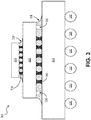
- Figure 3 is a cross-sectional view of a semiconductor package 300 having a plurality of bumps surrounded with a surface finish above and around the side walls of the bumps, according to one embodiment.
- Figure 3 illustrates the semiconductor package 300 including interconnect structures (e.g ., the plurality of bumps disposed below a die 314 and an interposer 312), according to some embodiments.
- the semiconductor package 300 may include a bump (or Cu bump/pad) that is surrounded with a surface finish (e.g ., NiPdAu surface finish) on the top surface and sidewalls of the bump (as shown in Figures 1 - 2 ).
- the semiconductor package 300 is merely one example of an embodiment wherein an integrated circuit die 314 is coupled to a substrate (e.g ., an interposer) 312 via one or more bumps/joints formed from respective microbumps.
- these bumps may be formed from the process flow shown in Figures 1A - ID and/or on the substrate 200 ( e.g ., bumps 115 of Figure 2 ).
- a solder joint formed by soldering of a microbump according to an embodiment may itself be referred to as a "bump" and/or a "microbump.”
- the semiconductor package 300 may have a die 314 disposed on an interposer 312, where both the stacked die 314 and interposer 312 are disposed on a package substrate 310.
- the package substrate 310 may include, but is not limited to, a package, a substrate, a printed circuit board (PCB), and a motherboard.
- the package substrate 310 is a PCB.
- the PCB is made of an FR-4 glass epoxy base with thin copper foil laminated on both sides (not shown).
- a multilayer PCB can be used, with pre-preg and copper foil (not shown) used to make additional layers.
- the multilayer PCB may include one or more dielectric layers, where each dielectric layer can be a photosensitive dielectric layer (not shown).
- holes may be drilled in the PCB 310.
- the PCB 310 may also include conductive copper traces, metallic pads, and holes (not shown).
- the die 314 may include, but is not limited to, a semiconductor die, an electronic device (e.g., a wireless device), an integrated circuit, a central processing unit (CPU), a microprocessor, a platform controller hub (PCH), a memory, and a field-programmable gate array (FPGA).
- the die 314 may be formed from a material such as silicon and have circuitry thereon that is to be coupled to the interposer 312.
- the package substrate 310 may in turn be coupled to another body, for example, a computer motherboard (not shown).
- One or more connections between the package substrate 310, the interposer 312, and the die 314 - e.g ., including some or all of bumps 316, 318, and 320 - may have a surface finish that may include NiPdAu metallurgy.
- these interconnect structures (or connections) may variously comprise an alloy of nickel, palladium, and tin (and, in some embodiments, copper).
- one or more of the bumps 316, 318, and/or 320 may include a NiPdAu surface finish that covers the top surfaces and the sidewalls of the bumps ( e.g ., as shown in Figure ID).
- the package substrate 310 may include a variety of electronic structures formed thereon or therein.
- the interposer 312 may also include electronic structures formed thereon or therein, which may be used to couple the die 314 to the package substrate 310.
- one or more different materials may be used for forming the package substrate and the interposer.
- the package substrate 310 is an organic substrate made up of one or more layers of polymer base material, with conducting regions for transmitting signals.
- the interposer 312 is made up of a ceramic base material including metal regions for transmitting signals.
- the semiconductor package 300 may include gap control structures 330 - e.g., positioned between the package substrate 310 and the interposer 312. Such gap control structures 330 may mitigate a change in the height of the gap between the package substrate 310 and the interposer 312, which otherwise might occur during reflowing while die 314 is attached to interposer 312.
- the semiconductor package 300 includes an underflow material 328 between the interposer 312 and the die 314, and an underflow material 326 between the package substrate 310 and the interposer 312.
- the underflow materials (or layers) 326 and 328 may be one or more polymers that are injected between the layers.
- semiconductor package 300 may include fewer or additional packaging components based on the desired packaging design.
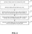
- Figure 4 is a process flow illustrating a method of a semiconductor package that includes a bump surrounded with a surface finish above and around each sidewall of the bump, according to one embodiment.
- the process flow 400 includes one or more steps used to form the semiconductor packages as described herein ( e.g., the semiconductor packages 100 of Figure 1 and 300 of Figure 3 ).
- the process flow 400 disposes a resist layer on a conductive layer ( e.g., as shown in Figure 1A ).
- the process flow 400 disposes a seed layer on the resist layer ( e.g., as shown in Figure 1A ).
- the process flow may also include disposing a dielectric layer on the seed layer.
- the process flow 400 disposes a bump on the conductive layer, where the bump has a top surface and one or more sidewalls ( e.g ., as shown in Figure 2 ).
- the process flow 400 recesses (or etches) between the dielectric layer and the bump to expose the one or more sidewalls of the bump (e.g ., the exposed sidewalls 113 as shown in Figure 1B and Figure 2 ).
- the bump may be etched on both the sidewalls and the top surface.
- the process flow 400 disposes a surface finish (e.g ., NiPdAu surface finish/layer) on the top surface and the one or more sidewalls of the bump ( e.g ., as shown in Figures 1C and ID).
- the process flow may include disposing/depositing a NiPdAu surface finish (e.g ., surface finish 140) on the top surface and the one or sidewalls of the bump ( e.g., the top surface 112 and sidewalls 113 of the bump 115).
- the process flow may remove/strip the dielectric layer and then the seed layer (e.g ., using an electroless Cu removal process) to expose the top surface of the resist layer (e.g., the top surface 130a of the resist 130 as shown in Figure ID).
- the seed layer e.g., using an electroless Cu removal process
- the process flow may have the surface finish be an electroless surface finish.
- the process flow may also include that the electroless surface finish is a nickel-palladium-gold (NiPdAu) surface finish (note that the surface finish may include one or more different materials and/or processing techniques).
- the process flow may dispose a seed on a top surface of the resist layer, and dispose a dielectric on the seed, where the dielectric surrounds the one or more sidewalls of the bump (as shown in Figure 1A ).
- the process flow may include that the seed is an electroless copper seed.
- the process flow may further form a gap opening between the dielectric and the one or more sidewalls of the bump, where the one or more sidewalls of the bump are exposed by the gap opening (as shown in Figure 1B ).
- the process flow may include that the bump is a copper bump.
- the process flow may have the dielectric to include a polymer material.
- the process flow may use the surface finish on (to cover/surround) a plurality of bumps that may be used to couple at least two or more of a die, an interposer, and a substrate.
- the semiconductor package formed by process flow 400 may include fewer or additional packaging components based on the desired packaging design ( e.g., as shown in Figures 1-3 ).
- FIG 5 is a schematic block diagram illustrating a computer system that utilizes a semiconductor package having a bump surrounded with a surface finish above and around each sidewall of the bump, according to one embodiment.
- Figure5 illustrates an example of computing device 500.
- Computing device 500 houses motherboard 502.
- motherboard 502 may be similar to the package substrate of Figure 3 ( e.g ., substrate 310 of Figure 3 ).
- Motherboard 502 may include a number of components, including but not limited to processor 504, semiconductor package 510, and at least one communication chip 506.
- Processor 504 is physically and electrically coupled to motherboard 502.
- at least one communication chip 506 is also physically and electrically coupled to motherboard 502.
- at least one communication chip 506 is part of processor 504.
- computing device 500 may include other components that may or may not be physically and electrically coupled to motherboard 502. These other components include, but are not limited to, volatile memory (e.g ., DRAM), non-volatile memory (e.g., ROM), flash memory, a graphics processor, a digital signal processor, a crypto processor, a chipset, an antenna, a display, a touchscreen display, a touchscreen controller, a battery, an audio codec, a video codec, a power amplifier, a global positioning system (GPS) device, a compass, an accelerometer, a gyroscope, a speaker, a camera, and a mass storage device (such as hard disk drive, compact disk (CD), digital versatile disk (DVD), and so forth).
- volatile memory e.g ., DRAM
- non-volatile memory e.g., ROM
- flash memory e.g., a graphics processor
- a digital signal processor e.g., ROM
- crypto processor e.
- At least one communication chip 506 enables wireless communications for the transfer of data to and from computing device 500.
- wireless and its derivatives may be used to describe circuits, devices, systems, methods, techniques, communications channels, etc., that may communicate data through the use of modulated electromagnetic radiation through a non-solid medium. The term does not imply that the associated devices do not contain any wires, although in some embodiments they might not.
- At least one communication chip 506 may implement any of a number of wireless standards or protocols, including but not limited to Wi-Fi (IEEE 802.11 family), WiMAX (IEEE 802.16 family), IEEE 802.20, long term evolution (LTE), Ev-DO, HSPA+, HSDPA+, HSUPA+, EDGE, GSM, GPRS, CDMA, TDMA, DECT, Bluetooth, derivatives thereof, as well as any other wireless protocols that are designated as 3G, 4G, 5G, and beyond.
- Computing device 500 may include a plurality of communication chips 406.
- a first communication chip 406 may be dedicated to shorter range wireless communications such as Wi-Fi and Bluetooth and a second communication chip 506 may be dedicated to longer range wireless communications such as GPS, EDGE, GPRS, CDMA, WiMAX, LTE, Ev-DO, and others.
- Processor 504 of computing device 500 includes an integrated circuit die packaged within processor 504.
- Device package 510 may be, but is not limited to, a packaging substrate and/or a printed circuit board.
- Device package 510 may be a semiconductor package with a bump surrounded with a surface finish above and around each sidewall of the bump (as illustrated in Figures 1-3 ) - or any other components from the figures described herein - of the computing device 500. Further, as described herein, the device package 510 may help lower the yield loss of the computing device 500 by mitigiating Galvanic corrosion in interconnecting structures (e.g., FLI) with the surface finish (e.g., NiPdAu) surrounding/covering the Cu interconnect structures - without increasing assembly costs, uncertainty, and time.
- interconnecting structures e.g., FLI
- the surface finish e.g., NiPdAu
- device package 510 may be a single component/device, a subset of components, and/or an entire system, as the materials, features, and components may be limited to device package 410 and/or any other component of the computing device 500 that may need the surface finish layer around the Cu interconnect structures (e.g ., Cu bump, Cu pad, microbump, bump/pad, etc.).
- the integrated circuit die may be packaged with one or more devices on a package substrate that includes a thermally stable RFIC and antenna for use with wireless communications and the device package, as described herein, to reduce the z-height of the computing device.
- the term "processor” may refer to any device or portion of a device that processes electronic data from registers and/or memory to transform that electronic data into other electronic data that may be stored in registers and/or memory.
- At least one communication chip 506 also includes an integrated circuit die packaged within the communication chip 506.
- the integrated circuit die of the communication chip may be packaged with one or more devices on a package substrate that includes one or more device packages, as described herein.
Landscapes
- Engineering & Computer Science (AREA)
- Manufacturing & Machinery (AREA)
- Microelectronics & Electronic Packaging (AREA)
- Wire Bonding (AREA)
- Internal Circuitry In Semiconductor Integrated Circuit Devices (AREA)
- Mechanical Treatment Of Semiconductor (AREA)
Abstract
Description
- Embodiments relate to packaging semiconductor devices. More particularly, the embodiments relate to packaging semiconductor devices having a bump (e.g., a copper (Cu) bump/pad) surrounded with a surface finish around each sidewall of the bump.
- Packaging of semiconductor devices, such as integrated circuits (ICs), present several problems. One of the main problems invovled with packaging ICs includes failure modes at the various interconnect levels (e.g., at a first-level interconnect (FLI)). These failure modes are typically associated with missing bumps and over-etched bumps at an interconnect level due to Galvanic corrosion.
- Glavnic corrosion is the electrochemical process in which a metal corrodes, especially as the metal electrically contacts another metal, in the presence of an electrolyte. This corrosion, for example, impacts the formation of ICs such as the fabrication of bumps to interconnect microelectronic devices. ICs are typically formed on a semiconductor wafer made of materials such as silicon. The semiconductor wafer is then processed to form various electronic devices. The wafers is usually diced into semiconductor chips (or dies), which may then be attached to a substrate. The substrate is typically designed to couple the die, directly or indirectly, to a printed circuit board (PCB), socket, or other connection. The substrate may also perform one or more other functions such as protecting, isolating, insulating, and/or thermally controlling the die.
- The substrate (e.g., an interposer) has traditionally been formed from a core made up of a laminated multilayer structure. Typically, bumps (or microbumps) and other such interconnect structures are variously formed in or on the structure to facilitate electrical coupling of a die to one or more other devices, such as at the FLI. As successive generations of fabrication technologies continue to scale in size, metallurgical properties of various materials have an increasingly significant impact on the formation and operation of interconnect structures.
- There is an increasing demand for incremental improvements in the fabrication of structures to interconnect microelectronic devices. These improvements are necessary in FLI structures as missing bumps due to Galvanic corrosion are prevalent contributors to FLI failure modes. A missing bump in Cu FLI generally occurs due to the potential difference between Cu and gold (Au) during the electroless Cu removal, as the Cu bump is connected to the Au-terminated die side capacitor (DSC) pad or the Au-terminated land side capacitor (LSC) pad (e.g., the yield loss of the device may increase to roughly 100% based on the FLI design). Some packaging solutions to reduce this yield loss associated to Galvanic corrosion may include optimizing the electroless Cu removal condition or developing new chemical properties that are less invasive. These packaging solutions, however, require increased assembly costs, uncertainty, and time. As such, there is an increased demand to mitigate Galvanic corrosion in interconnecting structures in ICs without increasing assembly costs, uncertainty, and time.
- Embodiments described herein illustrated by way of example and not limitation in the figures of the accompanying drawings, in which like references indicate similar features. Furthermore, some conventional details have been omitted so as not to obscure from the inventive concepts described herein.
-
Figures 1A - 1D are cross-sectional views of a process flow to form a semiconductor package having a bump surrounded with a surface finish above and around each sidewall of the bump, according to some embodiments. -
Figure 2 is a plan view of a semiconductor package having a dielectric layer with a plurality of bumps surrounded by a plurality of gap openings formed between each bump and the dielectric layer, according to one embodiment. -
Figure 3 is a cross-sectional view of a semiconductor package having a plurality of bumps surrounded with a surface finish above and around the side walls of the bumps, according to one embodiment. -
Figure 4 is a process flow illustrating a method of a semiconductor package that includes a bump surrounded with a surface finish above and around each sidewall of the bump, according to one embodiment. -
Figure 5 is a schematic block diagram illustrating a computer system that utilizes a semiconductor package having a bump surrounded with a surface finish above and around each sidewall of the bump, according to one embodiment. - Described herein are systems that include semiconductor packages with sidewall protection on one or more bumps (or copper (Cu) bumps) and methods of forming such semiconductor packages. According to some embodiments, the semiconductor package described below and methods of forming such semiconductor package include a resist layer on a conductive layer, a bump disposed on the conductive layer, where the bump has a top surface and one or more sidewalls, and a surface finish on the top surface and the one or more sidewalls of the bump. For one embodiment, the surface finish may include a nickel-palladium-gold (NiPdAu) surface (or plated) finish that surrounds the top surface and sidewalls of the bump, which enables Galvanic corrosion protection throughout the entire surface of the bump rather than disposing the surface finish only the top surface of the bump.
- In some semiconductor package (e.g., package on package (PoP)) substrates, there are more than one interconnect areas, such as PoP interconnects and controlled collapse chip connection (C4) interconnects, present on the same substrate. A surface finish deposited (or disposed) only on the top surface of the interconnects (or bumps) does not reduce failures (e.g., a missing bump) of the interconnects. To reduce the failures and improve the yield of the semiconductor packages, the embodiments described herein apply a surface finish (e.g., an electroless NiPdAu surface finish) to the one or more interconnect areas by disposing the surface finish on the top surface and sidewall(s) of each interconnect/bump. According to some embodiments, the surface finish can be used to provide good solder joint reliability (SJR) for the one or more interconnects and ultimately mitigate missing bumps due to Galvanic corrosion. A new substrate fabrication process (e.g., as shown in
Figures 1A - ID) can be used to etch the sidewalls of a bump (i.e., a gap is formed between the dielectric and the bump) and then dispose the surface finish above and around the top surface and sidewalls of the bump. Accordingly, these embodiments described herein enable a semiconductor package to have interconnect structures with no exposed Cu on both the top surface and the sidewalls of interconnect structures. - Embodiments of the semiconductor package enhance packaging solutions by protecting the interconnect structures with a NiPdAu surface finish (i.e., having no exposed Cu on the sidewalls of the Cu bump). For example, the NiPdAu surface finish has proven to be an excellent surface finish for SJR under electrical and thermal aging. Embodiments of the semiconductor package can further decrease the yield loss of the package (or devices) associated with one or more missing bumps and/or over-etched bumps. In addition, the embodiments of the semiconductor package help to maximize the surface area of a substrate in order to free up space for the die side capacitors (DSCs) and land side capacitors (LSCs) connections on the package. Furthermore, the embodiments of the semiconductor package, as described herein, help to mitigate Galvanic corrosion at a first-level interconnect (FLI) to decrease the FLI failure modes associated with missing bumps and/or over-etched bumps.
- Moreover, these embodiments described herein enhance the demand for improvements in the fabrication of structures to interconnect microelectronic devices using the NiPdAu surface finish. For example, the deposition of NiPdAu surface finish enables a decreased yield loss in Cu FLI structures as missing bumps due to Galvanic corrosion are mitigated. Accordingly, the embodiments described herein provide interconnect structures with a surface finish (e.g., a NiPdAu surface finish) that prevents (or significantly hinders) Galvanic corrosion in interconnect structures on the semiconductor package - without increasing assembly costs, uncertainty, and time.
- Note that, for some alternative embodiments, a variety of other surface finishes can be used such as, but not limited to, electrolytic NiPdAu, electrolytic PdAu, electrolytic NiPd, among others. Also note that while a NiPdAu process is illustrated herein a variety of other finishes suitable for one or more interconnect structures can be used depending on the application and/or desired packaging design.
- Lastly, the embodiments described herein provide techniques and mechanisms for improved protection of interconnect structures (e.g., bumps/pads, microbumps, Cu bumps, etc.). A bump may include any type of bumps that include a Cu seed layer, and the bump may also include a combination of one or more metals (e.g., Cu, Cu-NiPdAu, Cu-OSP, Cu-Sn, etc.). As used herein, a "bump" (also referred to herein as a "Cu bump," "bump," and/or a "microbump") is variously used to refer to at least one of a conductive contact (or pad) of a device and a solder joint (or a bump/pad) formed on such a conductive contact. In addition, a "bump" may refer to a solder joint formed by soldering with a microbump (where such a solder joint could also be referred to colloquially as a "microbump").
- The technologies described herein may be implemented in one or more electronic devices. Non-limiting examples of electronic devices that may utilize the technologies described herein include any kind of mobile device and/or stationary device, such as cameras, cell phones, computer terminals, desktop computers, electronic readers, facsimile machines, kiosks, netbook computers, notebook computers, internet devices, payment terminals, personal digital assistants, media players and/or recorders, servers (e.g., blade server, rack mount server, combinations thereof, etc.), set-top boxes, smart phones, tablet personal computers, ultra-mobile personal computers, wired telephones, combinations thereof, and the like. Such devices may be portable or stationary. In some embodiments, the technologies described herein may be employed in a desktop computer, laptop computer, smart phone, tablet computer, netbook computer, notebook computer, personal digital assistant, server, combinations thereof, and the like. More generally, the technologies described herein may be employed in any of a variety of electronic devices including a substrate including interconnect structures to provide connectivity to integrated circuitry.
- In the following description, various aspects of the illustrative implementations will be described using terms commonly employed by those skilled in the art to convey the substance of their work to others skilled in the art. However, it will be apparent to those skilled in the art that the present embodiments may be practiced with only some of the described aspects. For purposes of explanation, specific numbers, materials and configurations are set forth in order to provide a thorough understanding of the illustrative implementations. However, it will be apparent to one skilled in the art that the present embodiments may be practiced without the specific details. In other instances, well-known features are omitted or simplified in order not to obscure the illustrative implementations.
- Various operations will be described as multiple discrete operations, in turn, in a manner that is most helpful in understanding the present embodiments, however, the order of description should not be construed to imply that these operations are necessarily order dependent. In particular, these operations need not be performed in the order of presentation.
-
Figures 1A - ID are cross-sectional views of a process flow to form a semiconductor package having a bump surrounded with a surface finish above and around each sidewall of the bump, according to some embodiments. These embodiments as shown with respect toFigures 1A - ID provide a fabricating process to develop sidewall protection for interconnect structures for any desired packaging needs, including, but not limited to, missing bump reduction, over-etched bump reduction, and decreased yield loss and FLI failure modes. - One such embodiment is illustrated and described based on
Figures 1A - ID, which illustrates cross-sectional views of a package layer 100 (or substrate) used to form a Cu bump surrounded with a surface finish (e.g., NiPdAu). In the illustrated embodiments, the deposition of the surface finish on the bump is shown, however it is to be appreciated that additional features, such as additional components, bumps, layers, lines, vias, and/or pads, may be formed at the same time and with the same processing operations, according to the embodiments described herein. - Referring now to
Figure 1A , thepackage layer 100 may include a resistlayer 130 disposed on a conductive layer 120 (or an initial top metal layer (e.g., Cu layer)), where theconductive layer 120 may have one or more pads, vias, and/or traces. For one embodiment, thepackage layer 100 ofFigure 1A illustrates at least one interconnect layer of a semiconductor package (or substrate) that has theconductive layer 120 and the resistlayer 130. According to one embodiment, thispackage layer 100 is shown with theconductive layer 120 having an existing pad and via, but additional pads, vias, and traces may be formed below and coupled to the initial conductive layer 120 (which may be omitted for simplicity). - For one embodiment, the resist
layer 130 may be a solder resist layer, a solder mask, a solder stop mask, and/or any similar resist layer. The resistlayer 130 may be a thin layer of polymer(s) that is usually applied to the Cu traces (e.g., the conductive layer 120) of a package layer (e.g., a printed circuit board (PCB) or substrate) for protection against oxidation and to prevent solder bridges from forming between closely spaced bumps/pads. According to one embodiment, the resistlayer 130 may be an epoxy, a photoimageable solder mask, a photoimageable ink, and a dry film photoimageable solder mask. - As shown in
Figure 1A , aseed layer 122 is disposed on the resistlayer 130 and adielectric layer 110 is then disposed on theseed layer 122. For one embodiment, a bump 115 (e.g., a Cu bump) is disposed (or deposited) on theconductive layer 120 within an opening formed/patterned on thedielectric layer 110. According to some embodiments, theseed layer 122 is an electroless Cu seed layer that is deposited over a top surface of the resistlayer 130. For example, electroless plating or physical vapor deposition (i.e., sputtering) techniques may be used to deposit theseed layer 122. By way of illustration and not limitation, electroless plating of pure Cu may be used to form theseed layer 122 to have a desired thickness based on the packaging design/application (e.g., in a range of 0.1 µm to 2.0 µm, or any other desired thicknesses). In another embodiment, a combination of Cu and titanium (Ti) may be sputtered to form theseed layer 122. Note that theseed layer 122 may have any of various other material compositions and/or thicknesses, in alternative embodiments. - By way of example, the
dielectric layer 110 may be a polymer material, such as, for example, a dry film resist (DFR), a polyimide, an epoxy, or a build-up film (BF). In one embodiment, thedielectric layer 110 may be one layer in a stack that includes a plurality of dielectric layers used to form a build-up structure. As such, thedielectric layer 110 may be formed over another dielectric layer. Additional embodiments may include forming thedielectric layer 110 as the first dielectric layer over a core material on which the stack is formed. For one embodiment, thedielectric layer 110 is patterned to provide the opening for the formation of thebump 115 on theconductive layer 120. Accordingly, thebump 115 has atop surface 112 that is exposed (and, thus, formed between the dielectric layer 110). - Referring now to
Figure 1B , according to some embodiments, thebump 115 is etched between thedielectric layer 110 and thebump 115, providing one ormore gap openings 113 between the dielectric 110 and thebump 115. For the one embodiment, thebump 115 may be etched (or removed) on both the top surface and side walls to expose one or more sidewalls 114 using a Cu seed etching process (e.g., a controlled etching process) or the like. For some embodiments, the etching process provides the gap opening 113 which may extend vertically from thetop surface 112 of thebump 115 to the top surface of the resist layer 130 (i.e., thegap 113 extends through theseed layer 122 onto the top surface of the resist layer 130). Note that thebump 114 may have a single sidewall when the desired bump shape is circular, however thebump 114 may two or more sidewalls based on a different desired shape (e.g., a rectangular pad). In addition, as shown inFigure 2 with a top view of a package layer (similar to thepackage layer 100 ofFigure 1B ), the package layer may have a plurality of bumps (e.g., thebump 115 ofFigure 1B ) surrounded with a dielectric layer (e.g., thedielectric layer 110 ofFigure 1B ), where each bump has a gap opening (e.g.,gap 113 ofFigure 1B ) between the dielectric layer and a sidewall (e.g., thesidewall 114 ofFigure 1B ) of the bump. - Referring now to
Figure 1C , asurface finish 140 is deposited above and around thetop surface 112 and sidewall(s) 114 of thebump 115. For one embodiment, thesurface finish 140 may include a combination of Ni, Pd, and Au (i.e., a NiPdAu surface finish). Thesurface finish 140 may be an electroless deposition of NiPdAu on thetop surface 112 of thebump 115, and on the exposed gap opening(s) (i.e., the gap opening(s) 113 as shown inFigure 1B ) between the dielectric 110 and thesidewalls 114 of thebump 115. Note that thesurface finish 140 may be shown as having a rectangular shape surrounding thetop surface 112 andsidewalls 114 of thebump 115, however thesurface finish 140 may conform to any desired shape based on the gap openings and the shape of the bump (e.g., the surface finish may have a rounded shape, or a slanted (or tapered) shape). - Referring now to Figure ID, the
package layer 100 has thedielectric layer 110 removed, and the exposedseed layer 122 is then removed. According to one embodiment, theseed layer 122 may be removed with a seed etching process which exposes thetop surface 130a of the resistlayer 130. For an alternative embodiment, thebump 115 with thesurface finish 140 may be formed prior to the formation of a second dielectric layer (not shown). For one embodiment, the dielectric removal process may include a wet etch, a dry etch (e.g., a plasma etch), a wet blast, or a laser ablation (e.g., by using excimer laser). According to one additional embodiment, the depth controlled dielectric removal process may be performed only proximate to thebump 115. - As such, after the removal process illustrated in Figure ID, the package layer 100 (or a semiconductor package) may include a resist
layer 130 disposed on aconductive layer 120. Thepackage layer 100 may also have abump 115 disposed on theconductive layer 120, where thebump 115 has atop surface 112 and one or more sidewalls 114. The one or more sidewalls 114 may be exposed by forming a gap opening (e.g., gap opening 113 as shown inFigure 1B ) between adielectric layer 110 and thebump 115. In addition, thepackage layer 100 has a surface finish 140 (e.g., NiPdAu) disposed/deposited on thetop surface 112 and the one or more sidewalls 114 of thebump 115. - Accordingly, these embodiments as illustrated in
Figures 1A - ID enable both thetop surface 112 and sidewall(s) 114 of theCu bump 115 to be covered (or surrounded) with aNiPdAu surface finish 140. TheNiPdAu surface finish 140 thus provides sidewall (and top) protection of theCu bump 115, which helps theCu bump 115 to not be exposed and etched during the electroless Cu removal (as shown in Figure ID). This sidewall protection of thesurface finish 140, therefore, allows for a reduction in missing bumps and over-etched bumps associated with Galvanic corrosion. In addition, these embodiments as illustrated with the process flow ofFigures 1A - ID enable a semiconductor package to have (i) a decreased yield loss due to missing bumps (and/or over-etched bumps) and (ii) additional space to route/design the DSC/LSC connections. - Note that
package layer 100 ofFigures 1A - 1D may include fewer or additional packaging components based on the desired packaging design. -
Figure 2 is a plan view of a semiconductor package 200 (or substrate) having adielectric layer 110 with a plurality ofbumps 115 surrounded bygap openings 113, according to one embodiment. Note that thesemiconductor package 200 ofFigure 2 is similar to thepackage layer 100 ofFigures 1A - 1D , however thesemiconductor package 200 includes a plurality ofbumps 115. As such, the process flow illustrated inFigures 1A - 1D may be used to form thesemiconductor package 200. - For one embodiment, the
gap openings 113 may be formed between eachbump 115 and thedielectric layer 110, where thegap openings 113 may be formed with a Cu etching process (as shown inFigure 1B ). According to one embodiment, thesemiconductor package 200 may have thedielectric layer 110 formed with a plurality ofbumps 115. Thedielectric layer 110 may surround eachbump 115 and have agap opening 113 formed between thedielectric layer 100 and one or more sidewalls 114 of eachbump 115. - Note that the
semiconductor package 200 may include fewer or additional packaging components based on the desired packaging design. -
Figure 3 is a cross-sectional view of asemiconductor package 300 having a plurality of bumps surrounded with a surface finish above and around the side walls of the bumps, according to one embodiment. Specifically,Figure 3 illustrates thesemiconductor package 300 including interconnect structures (e.g., the plurality of bumps disposed below adie 314 and an interposer 312), according to some embodiments. For one embodiment, thesemiconductor package 300 may include a bump (or Cu bump/pad) that is surrounded with a surface finish (e.g., NiPdAu surface finish) on the top surface and sidewalls of the bump (as shown inFigures 1 - 2 ). - The
semiconductor package 300 is merely one example of an embodiment wherein an integrated circuit die 314 is coupled to a substrate (e.g., an interposer) 312 via one or more bumps/joints formed from respective microbumps. For example, these bumps may be formed from the process flow shown inFigures 1A - ID and/or on the substrate 200 (e.g., bumps 115 ofFigure 2 ). As described above, a solder joint formed by soldering of a microbump according to an embodiment may itself be referred to as a "bump" and/or a "microbump." - For some embodiments, the
semiconductor package 300 may have a die 314 disposed on aninterposer 312, where both thestacked die 314 andinterposer 312 are disposed on apackage substrate 310. According to some embodiments, thepackage substrate 310 may include, but is not limited to, a package, a substrate, a printed circuit board (PCB), and a motherboard. For one embodiment, thepackage substrate 310 is a PCB. For one embodiment, the PCB is made of an FR-4 glass epoxy base with thin copper foil laminated on both sides (not shown). For certain embodiments, a multilayer PCB can be used, with pre-preg and copper foil (not shown) used to make additional layers. For example, the multilayer PCB may include one or more dielectric layers, where each dielectric layer can be a photosensitive dielectric layer (not shown). For some embodiments, holes (not shown) may be drilled in thePCB 310. For one embodiment, thePCB 310 may also include conductive copper traces, metallic pads, and holes (not shown). - For one embodiment, the
die 314 may include, but is not limited to, a semiconductor die, an electronic device (e.g., a wireless device), an integrated circuit, a central processing unit (CPU), a microprocessor, a platform controller hub (PCH), a memory, and a field-programmable gate array (FPGA). Thedie 314 may be formed from a material such as silicon and have circuitry thereon that is to be coupled to theinterposer 312. Although some embodiments are not limited in this regard, thepackage substrate 310 may in turn be coupled to another body, for example, a computer motherboard (not shown). One or more connections between thepackage substrate 310, theinterposer 312, and the die 314 - e.g., including some or all ofbumps bumps - Connections between the
package substrate 310 and another body may be made using any suitable structure, such as theillustrative bumps 320 shown. Thepackage substrate 310 may include a variety of electronic structures formed thereon or therein. Theinterposer 312 may also include electronic structures formed thereon or therein, which may be used to couple the die 314 to thepackage substrate 310. For one embodiment, one or more different materials may be used for forming the package substrate and the interposer. In certain embodiments, thepackage substrate 310 is an organic substrate made up of one or more layers of polymer base material, with conducting regions for transmitting signals. In certain embodiments, theinterposer 312 is made up of a ceramic base material including metal regions for transmitting signals. Although some embodiments are not limited in this regard, thesemiconductor package 300 may include gap control structures 330 - e.g., positioned between thepackage substrate 310 and theinterposer 312. Suchgap control structures 330 may mitigate a change in the height of the gap between thepackage substrate 310 and theinterposer 312, which otherwise might occur during reflowing while die 314 is attached tointerposer 312. Note that thesemiconductor package 300 includes anunderflow material 328 between theinterposer 312 and thedie 314, and anunderflow material 326 between thepackage substrate 310 and theinterposer 312. The underflow materials (or layers) 326 and 328 may be one or more polymers that are injected between the layers. - Note that the
semiconductor package 300 may include fewer or additional packaging components based on the desired packaging design. -
Figure 4 is a process flow illustrating a method of a semiconductor package that includes a bump surrounded with a surface finish above and around each sidewall of the bump, according to one embodiment. For one embodiment, the process flow 400 includes one or more steps used to form the semiconductor packages as described herein (e.g., the semiconductor packages 100 ofFigure 1 and 300 ofFigure 3 ). - At
block 405, the process flow 400 disposes a resist layer on a conductive layer (e.g., as shown inFigure 1A ). Atblock 410, the process flow 400 disposes a seed layer on the resist layer (e.g., as shown inFigure 1A ). In addition, the process flow may also include disposing a dielectric layer on the seed layer. Atblock 415, the process flow 400 disposes a bump on the conductive layer, where the bump has a top surface and one or more sidewalls (e.g., as shown inFigure 2 ). Atblock 420, the process flow 400 recesses (or etches) between the dielectric layer and the bump to expose the one or more sidewalls of the bump (e.g., the exposed sidewalls 113 as shown inFigure 1B andFigure 2 ). For example, the bump may be etched on both the sidewalls and the top surface. - At
block 425, the process flow 400 disposes a surface finish (e.g., NiPdAu surface finish/layer) on the top surface and the one or more sidewalls of the bump (e.g., as shown inFigures 1C and ID). For example, the process flow may include disposing/depositing a NiPdAu surface finish (e.g., surface finish 140) on the top surface and the one or sidewalls of the bump (e.g., thetop surface 112 andsidewalls 113 of the bump 115). In addition, the process flow may remove/strip the dielectric layer and then the seed layer (e.g., using an electroless Cu removal process) to expose the top surface of the resist layer (e.g., thetop surface 130a of the resist 130 as shown in Figure ID). - For additional embodiments, the process flow may have the surface finish be an electroless surface finish. The process flow may also include that the electroless surface finish is a nickel-palladium-gold (NiPdAu) surface finish (note that the surface finish may include one or more different materials and/or processing techniques). Moreover, the process flow may dispose a seed on a top surface of the resist layer, and dispose a dielectric on the seed, where the dielectric surrounds the one or more sidewalls of the bump (as shown in
Figure 1A ). The process flow may include that the seed is an electroless copper seed. The process flow may further form a gap opening between the dielectric and the one or more sidewalls of the bump, where the one or more sidewalls of the bump are exposed by the gap opening (as shown inFigure 1B ). The process flow may include that the bump is a copper bump. In addition, the process flow may have the dielectric to include a polymer material. In addition, the process flow may use the surface finish on (to cover/surround) a plurality of bumps that may be used to couple at least two or more of a die, an interposer, and a substrate. - Note that the semiconductor package formed by process flow 400 may include fewer or additional packaging components based on the desired packaging design (e.g., as shown in
Figures 1-3 ). -
Figure 5 is a schematic block diagram illustrating a computer system that utilizes a semiconductor package having a bump surrounded with a surface finish above and around each sidewall of the bump, according to one embodiment.Figure5 illustrates an example ofcomputing device 500.Computing device 500houses motherboard 502. For one embodiment,motherboard 502 may be similar to the package substrate ofFigure 3 (e.g.,substrate 310 ofFigure 3 ).Motherboard 502 may include a number of components, including but not limited toprocessor 504,semiconductor package 510, and at least onecommunication chip 506.Processor 504 is physically and electrically coupled tomotherboard 502. For some embodiments, at least onecommunication chip 506 is also physically and electrically coupled tomotherboard 502. For other embodiments, at least onecommunication chip 506 is part ofprocessor 504. - Depending on its applications,
computing device 500 may include other components that may or may not be physically and electrically coupled tomotherboard 502. These other components include, but are not limited to, volatile memory (e.g., DRAM), non-volatile memory (e.g., ROM), flash memory, a graphics processor, a digital signal processor, a crypto processor, a chipset, an antenna, a display, a touchscreen display, a touchscreen controller, a battery, an audio codec, a video codec, a power amplifier, a global positioning system (GPS) device, a compass, an accelerometer, a gyroscope, a speaker, a camera, and a mass storage device (such as hard disk drive, compact disk (CD), digital versatile disk (DVD), and so forth). - At least one
communication chip 506 enables wireless communications for the transfer of data to and fromcomputing device 500. The term "wireless" and its derivatives may be used to describe circuits, devices, systems, methods, techniques, communications channels, etc., that may communicate data through the use of modulated electromagnetic radiation through a non-solid medium. The term does not imply that the associated devices do not contain any wires, although in some embodiments they might not. At least onecommunication chip 506 may implement any of a number of wireless standards or protocols, including but not limited to Wi-Fi (IEEE 802.11 family), WiMAX (IEEE 802.16 family), IEEE 802.20, long term evolution (LTE), Ev-DO, HSPA+, HSDPA+, HSUPA+, EDGE, GSM, GPRS, CDMA, TDMA, DECT, Bluetooth, derivatives thereof, as well as any other wireless protocols that are designated as 3G, 4G, 5G, and beyond.Computing device 500 may include a plurality of communication chips 406. For instance, a first communication chip 406 may be dedicated to shorter range wireless communications such as Wi-Fi and Bluetooth and asecond communication chip 506 may be dedicated to longer range wireless communications such as GPS, EDGE, GPRS, CDMA, WiMAX, LTE, Ev-DO, and others. -
Processor 504 ofcomputing device 500 includes an integrated circuit die packaged withinprocessor 504.Device package 510 may be, but is not limited to, a packaging substrate and/or a printed circuit board.Device package 510 may be a semiconductor package with a bump surrounded with a surface finish above and around each sidewall of the bump (as illustrated inFigures 1-3 ) - or any other components from the figures described herein - of thecomputing device 500. Further, as described herein, thedevice package 510 may help lower the yield loss of thecomputing device 500 by mitigiating Galvanic corrosion in interconnecting structures (e.g., FLI) with the surface finish (e.g., NiPdAu) surrounding/covering the Cu interconnect structures - without increasing assembly costs, uncertainty, and time. - Note that
device package 510 may be a single component/device, a subset of components, and/or an entire system, as the materials, features, and components may be limited todevice package 410 and/or any other component of thecomputing device 500 that may need the surface finish layer around the Cu interconnect structures (e.g., Cu bump, Cu pad, microbump, bump/pad, etc.). - For certain embodiments, the integrated circuit die may be packaged with one or more devices on a package substrate that includes a thermally stable RFIC and antenna for use with wireless communications and the device package, as described herein, to reduce the z-height of the computing device. The term "processor" may refer to any device or portion of a device that processes electronic data from registers and/or memory to transform that electronic data into other electronic data that may be stored in registers and/or memory.
- At least one
communication chip 506 also includes an integrated circuit die packaged within thecommunication chip 506. For some embodiments, the integrated circuit die of the communication chip may be packaged with one or more devices on a package substrate that includes one or more device packages, as described herein. - In the foregoing specification, embodiments have been described with reference to specific exemplary embodiments thereof. It should be borne in mind, however, that all of these and similar terms are to be associated with the appropriate physical quantities and are merely convenient labels applied to these quantities. It will be evident that various modifications may be made thereto without departing from the broader spirit and scope. The specification and drawings are, accordingly, to be regarded in an illustrative sense rather than a restrictive sense.
- The following examples pertain to further embodiments. The various features of the different embodiments may be variously combined with some features included and others excluded to suit a variety of different applications.
- The following examples pertain to further embodiments:
- Example 1 is a semiconductor package, comprising a resist layer on a conductive layer and a bump on the conductive layer. The bump has a top surface and one or more sidewalls; and a surface finish on the top surface and the one or more sidewalls of the bump.
- In Example 2, the subject matter of example 1 can optionally include the surface finish that surrounds the top surface and the one or more sidewalls of the bump to protect the bump from corrosion.
- In Example 3, the subject matter of any of examples 1-2 can optionally include the surface finish as a nickel-palladium-gold (NiPdAu) surface finish.
- In Example 4, the subject matter of any of examples 1-3 can optionally include further comprising a seed on a top surface of the resist layer; and a dielectric on the seed. The dielectric surrounds the one or more sidewalls of the bump.
- In Example 5, the subject matter of any of examples 1-4 can optionally include the seed as an electroless copper seed.
- In Example 6, the subject matter of any of examples 1-5 can optionally include further comprising a gap opening formed between the dielectric and the one or more sidewalls of the bump. The one or more sidewalls of the bump are exposed by the gap opening.
- In Example 7, the subject matter of any of examples 1-6 can optionally include the bump as a copper bump.
- In Example 8, the subject matter of any of examples 1-7 can optionally include the dielectric which includes a polymer material.
- Example 9 is a method of forming a semiconductor package, comprising of disposing a resist layer on a conductive layer and disposing a bump on the conductive layer. The bump has a top surface and one or more sidewalls; and disposing a surface finish on the top surface and the one or more sidewalls of the bump.
- In Example 10, the subject matter of example 9 can optionally include the surface finish surrounding the top surface and the one or more sidewalls of the bump to protect the bump from corrosion.
- In Example 11, the subject matter of any of examples 9-10 can optionally include the surface finish as a nickel-palladium-gold (NiPdAu) surface finish.
- In Example 12, the subject matter of any of examples 9-11 can optionally include further comprising disposing a seed on a top surface of the resist layer; and disposing a dielectric on the seed. The dielectric surrounds the one or more sidewalls of the bump.
- In Example 13, the subject matter of any of examples 9-12 can optionally include the seed as an electroless copper seed.
- In Example 14, the subject matter of any of examples 9-13 can optionally include further comprising forming a gap opening between the dielectric and the one or more sidewalls of the bump. The one or more sidewalls of the bump are exposed by the gap opening.
- In Example 15, the subject matter of any of examples 9-14 can optionally include the bump as a copper bump.
- In Example 16, the subject matter of any of examples 9-15 can optionally include the dielectric which includes a polymer material.
- Example 17 is a semiconductor package, comprising an interposer on a substrate; a die on the interposer; and a surface finish on a plurality of bumps. The plurality of bumps electrically couple the die to the interposer, and the interposer to the substrate.
- In Example 18, the subject matter of example 17 can optionally include the surface finish surrounding the top surface and the one or more sidewalls of the bumps to protect the bumps from corrosion. Each bump has at least a top surface and one or more sidewalls. The surface finish is disposed on at least one of the top surface and the one or more sidewalls of each bump.
- In Example 19, the subject matter of any of examples 17-18 can optionally include the surface finish as a nickel-palladium-gold (NiPdAu) surface finish.
- In Example 20, the subject matter of any of examples 17-19 can optionally include the plurality of bumps which include a metallic material. The metallic material includes copper.
- In Example 21, the subject matter of any of examples 17-20 can optionally include further comprising one or more underfill layers surrounding the plurality of bump.
- In Example 22, the subject matter of any of examples 17-21 can optionally include the substrate which includes a package and a printed circuit board.
- In Example 23, the subject matter of any of examples 17-22 can optionally include the die which includes an integrated circuit, a central processing unit, a microprocessor, a platform controller hub, a memory, and a field-programmable gate array.
- In Example 24, the subject matter of any of examples 17-23 can optionally include further comprising a plurality of bumps electrically coupling the substrate to a second substrate.
- In Example 25, the subject matter of any of examples 17-24 can optionally include the second substrate which includes a motherboard.
- In the foregoing specification, methods and apparatuses have been described with reference to specific exemplary embodiments thereof. It will be evident that various modifications may be made thereto without departing from the broader spirit and scope. The specification and drawings are, accordingly, to be regarded in an illustrative sense rather than a restrictive sense.
Claims (15)
- A semiconductor package, comprising:a resist layer on a conductive layer;a bump on the conductive layer, wherein the bump has a top surface and one or more sidewalls; anda surface finish on the top surface and the one or more sidewalls of the bump.
- The semiconductor package of claim 1, wherein the surface finish surrounds the top surface and the one or more sidewalls of the bump to protect the bump from corrosion.
- The semiconductor package of claims 1-2, wherein the surface finish is a nickel-palladium-gold (NiPdAu) surface finish.
- The semiconductor package of claims 1-3, further comprising:a seed on a top surface of the resist layer; anda dielectric on the seed, wherein the dielectric surrounds the one or more sidewalls of the bump.
- The semiconductor package of claims 1-4, wherein the seed is an electroless copper seed.
- The semiconductor package of claims 1-5, further comprising a gap opening formed between the dielectric and the one or more sidewalls of the bump, wherein the one or more sidewalls of the bump are exposed by the gap opening.
- The semiconductor package of claims 1-6, wherein the bump is a copper bump.
- The semiconductor package of claims 1-7, wherein the dielectric includes a polymer material.
- A method of forming a semiconductor package, comprising:disposing a resist layer on a conductive layer;disposing a bump on the conductive layer, wherein the bump has a top surface and one or more sidewalls; anddisposing a surface finish on the top surface and the one or more sidewalls of the bump.
- The method of claim 9, wherein the surface finish surrounds the top surface and the one or more sidewalls of the bump to protect the bump from corrosion.
- The method of claims 9-10, wherein the surface finish is a nickel-palladium-gold (NiPdAu) surface finish.
- The method of claim 9-11, further comprising:disposing a seed on a top surface of the resist layer; anddisposing a dielectric on the seed, wherein the dielectric surrounds the one or more sidewalls of the bump.
- The method of claims 9-12, wherein the seed is an electroless copper seed.
- The method of claims 9-13, further comprising forming a gap opening between the dielectric and the one or more sidewalls of the bump, wherein the one or more sidewalls of the bump are exposed by the gap opening.
- The method of claims 9-14, wherein the bump is a copper bump.
Applications Claiming Priority (1)
| Application Number | Priority Date | Filing Date | Title |
|---|---|---|---|
| US15/859,481 US20190206822A1 (en) | 2017-12-30 | 2017-12-30 | Missing bump prevention from galvanic corrosion by copper bump sidewall protection |
Publications (1)
| Publication Number | Publication Date |
|---|---|
| EP3506338A1 true EP3506338A1 (en) | 2019-07-03 |
Family
ID=64572107
Family Applications (1)
| Application Number | Title | Priority Date | Filing Date |
|---|---|---|---|
| EP18209353.4A Pending EP3506338A1 (en) | 2017-12-30 | 2018-11-29 | Prevention of missing bump due to galvanic corrosion by means of copper bump sidewall protection |
Country Status (3)
| Country | Link |
|---|---|
| US (1) | US20190206822A1 (en) |
| EP (1) | EP3506338A1 (en) |
| CN (1) | CN110034023A (en) |
Families Citing this family (3)
| Publication number | Priority date | Publication date | Assignee | Title |
|---|---|---|---|---|
| JP7142604B2 (en) * | 2019-05-15 | 2022-09-27 | 日本特殊陶業株式会社 | Wiring board and its manufacturing method |
| US12014969B2 (en) | 2021-08-30 | 2024-06-18 | Taiwan Semiconductor Manufacturing Company, Ltd. | Package structure and method for forming the same |
| JP2024008020A (en) * | 2022-07-07 | 2024-01-19 | 新光電気工業株式会社 | Wiring board and wiring board manufacturing method |
Citations (5)
| Publication number | Priority date | Publication date | Assignee | Title |
|---|---|---|---|---|
| JPS63122248A (en) * | 1986-11-12 | 1988-05-26 | Nec Corp | Manufacture of semiconductor device |
| US20110186989A1 (en) * | 2010-02-04 | 2011-08-04 | Taiwan Semiconductor Manufacturing Company, Ltd. | Semiconductor Device and Bump Formation Process |
| US8492891B2 (en) * | 2010-04-22 | 2013-07-23 | Taiwan Semiconductor Manufacturing Company, Ltd. | Cu pillar bump with electrolytic metal sidewall protection |
| TW201336002A (en) * | 2012-02-17 | 2013-09-01 | 頎邦科技股份有限公司 | Fine pitch bump manufacturing method and structure thereof |
| US9263390B2 (en) * | 2009-09-29 | 2016-02-16 | Semiconductor Components Industries, Llc | Semiconductor component that includes a protective structure |
Family Cites Families (8)
| Publication number | Priority date | Publication date | Assignee | Title |
|---|---|---|---|---|
| US6593220B1 (en) * | 2002-01-03 | 2003-07-15 | Taiwan Semiconductor Manufacturing Company | Elastomer plating mask sealed wafer level package method |
| TWI296184B (en) * | 2006-06-06 | 2008-04-21 | Phoenix Prec Technology Corp | Method for fabricating electrical connecting structure of circuit board |
| DE102006062473A1 (en) * | 2006-12-28 | 2008-07-03 | Qimonda Ag | Semiconductor device for use in semiconductor component, has chip with active and rear sides, where chip is arranged over one side of substrate, and completely encapsulated with only one material |
| TWI339883B (en) * | 2007-02-02 | 2011-04-01 | Unimicron Technology Corp | Substrate structure for semiconductor package and manufacturing method thereof |
| JP2011171567A (en) * | 2010-02-19 | 2011-09-01 | Elpida Memory Inc | Method of manufacturing substrate structure, and method of manufacturing semiconductor device |
| US10497660B2 (en) * | 2015-02-26 | 2019-12-03 | Taiwan Semiconductor Manufacturing Company, Ltd. | Interconnect structures, packaged semiconductor devices, and methods of packaging semiconductor devices |
| US9960102B2 (en) * | 2016-06-13 | 2018-05-01 | Advanced Semiconductor Engineering, Inc. | Semiconductor devices and methods of manufacturing the same |
| US10515888B2 (en) * | 2017-09-18 | 2019-12-24 | Taiwan Semiconductor Manufacturing Company Ltd. | Semiconductor device and method for manufacturing the same |
-
2017
- 2017-12-30 US US15/859,481 patent/US20190206822A1/en not_active Abandoned
-
2018
- 2018-11-29 EP EP18209353.4A patent/EP3506338A1/en active Pending
- 2018-11-30 CN CN201811455016.6A patent/CN110034023A/en active Pending
Patent Citations (5)
| Publication number | Priority date | Publication date | Assignee | Title |
|---|---|---|---|---|
| JPS63122248A (en) * | 1986-11-12 | 1988-05-26 | Nec Corp | Manufacture of semiconductor device |
| US9263390B2 (en) * | 2009-09-29 | 2016-02-16 | Semiconductor Components Industries, Llc | Semiconductor component that includes a protective structure |
| US20110186989A1 (en) * | 2010-02-04 | 2011-08-04 | Taiwan Semiconductor Manufacturing Company, Ltd. | Semiconductor Device and Bump Formation Process |
| US8492891B2 (en) * | 2010-04-22 | 2013-07-23 | Taiwan Semiconductor Manufacturing Company, Ltd. | Cu pillar bump with electrolytic metal sidewall protection |
| TW201336002A (en) * | 2012-02-17 | 2013-09-01 | 頎邦科技股份有限公司 | Fine pitch bump manufacturing method and structure thereof |
Also Published As
| Publication number | Publication date |
|---|---|
| US20190206822A1 (en) | 2019-07-04 |
| CN110034023A (en) | 2019-07-19 |
Similar Documents
| Publication | Publication Date | Title |
|---|---|---|
| US20240030086A1 (en) | Bga stim package architecture for high performance systems | |
| US10147710B2 (en) | Method of embedding WLCSP components in E-WLB and E-PLB | |
| KR101907733B1 (en) | Bridge interconnection with layered interconnect structures | |
| EP3117456B1 (en) | Microelectronic package having a passive microelectronic device disposed within a package body and its manufacturing method | |
| US9842800B2 (en) | Forming interconnect structures utilizing subtractive paterning techniques | |
| US20200098698A1 (en) | Novel wafer level chip scale package (wlcsp), flip-chip chip scale package (fccsp), and fan out shielding concepts | |
| US12573536B2 (en) | Electronic substrates having embedded inductors | |
| NL2028989B1 (en) | Electronic substrates having embedded inductors | |
| US10361165B2 (en) | Microelectronic substrate having embedded trace layers with integral attachment structures | |
| EP3506338A1 (en) | Prevention of missing bump due to galvanic corrosion by means of copper bump sidewall protection | |
| US12159844B2 (en) | Electronic substrates having embedded inductors | |
| US20190244922A1 (en) | Nickel-tin microbump structures and method of making same | |
| KR20130123725A (en) | Stacked semiconductor package and method for manufacturing the same | |
| US10373900B2 (en) | Tin-zinc microbump structures and method of making same | |
| US20260005167A1 (en) | Contamination free copper interconnect on aluminum pad | |
| US20230091379A1 (en) | First level interconnect under bump metallizations for fine pitch heterogeneous applications |
Legal Events
| Date | Code | Title | Description |
|---|---|---|---|
| PUAI | Public reference made under article 153(3) epc to a published international application that has entered the european phase |
Free format text: ORIGINAL CODE: 0009012 |
|
| STAA | Information on the status of an ep patent application or granted ep patent |
Free format text: STATUS: THE APPLICATION HAS BEEN PUBLISHED |
|
| AK | Designated contracting states |
Kind code of ref document: A1 Designated state(s): AL AT BE BG CH CY CZ DE DK EE ES FI FR GB GR HR HU IE IS IT LI LT LU LV MC MK MT NL NO PL PT RO RS SE SI SK SM TR |
|
| AX | Request for extension of the european patent |
Extension state: BA ME |
|
| STAA | Information on the status of an ep patent application or granted ep patent |
Free format text: STATUS: REQUEST FOR EXAMINATION WAS MADE |
|
| 17P | Request for examination filed |
Effective date: 20200103 |
|
| RBV | Designated contracting states (corrected) |
Designated state(s): AL AT BE BG CH CY CZ DE DK EE ES FI FR GB GR HR HU IE IS IT LI LT LU LV MC MK MT NL NO PL PT RO RS SE SI SK SM TR |
|
| STAA | Information on the status of an ep patent application or granted ep patent |
Free format text: STATUS: EXAMINATION IS IN PROGRESS |
|
| 17Q | First examination report despatched |
Effective date: 20230718 |