EP3506327A1 - Photoelectric conversion element - Google Patents
Photoelectric conversion element Download PDFInfo
- Publication number
- EP3506327A1 EP3506327A1 EP17843663.0A EP17843663A EP3506327A1 EP 3506327 A1 EP3506327 A1 EP 3506327A1 EP 17843663 A EP17843663 A EP 17843663A EP 3506327 A1 EP3506327 A1 EP 3506327A1
- Authority
- EP
- European Patent Office
- Prior art keywords
- sealing portion
- resin sealing
- photoelectric conversion
- main body
- electrode substrate
- Prior art date
- Legal status (The legal status is an assumption and is not a legal conclusion. Google has not performed a legal analysis and makes no representation as to the accuracy of the status listed.)
- Withdrawn
Links
- 238000006243 chemical reaction Methods 0.000 title claims abstract description 106
- 238000007789 sealing Methods 0.000 claims abstract description 314
- 239000000758 substrate Substances 0.000 claims abstract description 260
- 229920005989 resin Polymers 0.000 claims abstract description 228
- 239000011347 resin Substances 0.000 claims abstract description 228
- 239000003792 electrolyte Substances 0.000 claims abstract description 29
- 238000003780 insertion Methods 0.000 claims abstract description 23
- 230000037431 insertion Effects 0.000 claims abstract description 22
- 238000002844 melting Methods 0.000 claims abstract description 21
- 230000008018 melting Effects 0.000 claims abstract description 21
- 229920005992 thermoplastic resin Polymers 0.000 claims abstract description 13
- 239000004065 semiconductor Substances 0.000 claims description 51
- QVGXLLKOCUKJST-UHFFFAOYSA-N atomic oxygen Chemical compound [O] QVGXLLKOCUKJST-UHFFFAOYSA-N 0.000 claims description 30
- 229910052760 oxygen Inorganic materials 0.000 claims description 30
- 239000001301 oxygen Substances 0.000 claims description 30
- 230000035699 permeability Effects 0.000 claims description 21
- IMROMDMJAWUWLK-UHFFFAOYSA-N Ethenol Chemical group OC=C IMROMDMJAWUWLK-UHFFFAOYSA-N 0.000 claims description 4
- 239000010410 layer Substances 0.000 description 82
- 239000000975 dye Substances 0.000 description 29
- 239000011521 glass Substances 0.000 description 13
- 239000003054 catalyst Substances 0.000 description 11
- 239000002243 precursor Substances 0.000 description 10
- 230000000052 comparative effect Effects 0.000 description 7
- 239000002245 particle Substances 0.000 description 7
- 238000001035 drying Methods 0.000 description 6
- 239000002608 ionic liquid Substances 0.000 description 6
- 238000000034 method Methods 0.000 description 6
- 239000003960 organic solvent Substances 0.000 description 6
- BASFCYQUMIYNBI-UHFFFAOYSA-N platinum Chemical compound [Pt] BASFCYQUMIYNBI-UHFFFAOYSA-N 0.000 description 6
- XMBWDFGMSWQBCA-UHFFFAOYSA-N hydrogen iodide Chemical compound I XMBWDFGMSWQBCA-UHFFFAOYSA-N 0.000 description 5
- 239000011810 insulating material Substances 0.000 description 5
- 230000014759 maintenance of location Effects 0.000 description 5
- 230000002093 peripheral effect Effects 0.000 description 5
- 238000012360 testing method Methods 0.000 description 5
- 229920000219 Ethylene vinyl alcohol Polymers 0.000 description 4
- 150000001450 anions Chemical class 0.000 description 4
- 230000006866 deterioration Effects 0.000 description 4
- 238000010304 firing Methods 0.000 description 4
- XMBWDFGMSWQBCA-UHFFFAOYSA-M iodide Chemical compound [I-] XMBWDFGMSWQBCA-UHFFFAOYSA-M 0.000 description 4
- 238000007639 printing Methods 0.000 description 4
- XOLBLPGZBRYERU-UHFFFAOYSA-N tin dioxide Chemical compound O=[Sn]=O XOLBLPGZBRYERU-UHFFFAOYSA-N 0.000 description 4
- 229910001887 tin oxide Inorganic materials 0.000 description 4
- WEVYAHXRMPXWCK-UHFFFAOYSA-N Acetonitrile Chemical compound CC#N WEVYAHXRMPXWCK-UHFFFAOYSA-N 0.000 description 3
- VYPSYNLAJGMNEJ-UHFFFAOYSA-N Silicium dioxide Chemical compound O=[Si]=O VYPSYNLAJGMNEJ-UHFFFAOYSA-N 0.000 description 3
- RTAQQCXQSZGOHL-UHFFFAOYSA-N Titanium Chemical compound [Ti] RTAQQCXQSZGOHL-UHFFFAOYSA-N 0.000 description 3
- 239000000654 additive Substances 0.000 description 3
- 230000000996 additive effect Effects 0.000 description 3
- 230000015572 biosynthetic process Effects 0.000 description 3
- 238000010438 heat treatment Methods 0.000 description 3
- 229910052740 iodine Inorganic materials 0.000 description 3
- 150000002500 ions Chemical class 0.000 description 3
- 239000000463 material Substances 0.000 description 3
- 229910052697 platinum Inorganic materials 0.000 description 3
- -1 polyethylene terephthalate Polymers 0.000 description 3
- 150000003839 salts Chemical class 0.000 description 3
- 239000002356 single layer Substances 0.000 description 3
- 239000002904 solvent Substances 0.000 description 3
- 238000004544 sputter deposition Methods 0.000 description 3
- 239000000126 substance Substances 0.000 description 3
- HYZJCKYKOHLVJF-UHFFFAOYSA-N 1H-benzimidazole Chemical compound C1=CC=C2NC=NC2=C1 HYZJCKYKOHLVJF-UHFFFAOYSA-N 0.000 description 2
- JFJNVIPVOCESGZ-UHFFFAOYSA-N 2,3-dipyridin-2-ylpyridine Chemical group N1=CC=CC=C1C1=CC=CN=C1C1=CC=CC=N1 JFJNVIPVOCESGZ-UHFFFAOYSA-N 0.000 description 2
- OOWFYDWAMOKVSF-UHFFFAOYSA-N 3-methoxypropanenitrile Chemical compound COCCC#N OOWFYDWAMOKVSF-UHFFFAOYSA-N 0.000 description 2
- YEJRWHAVMIAJKC-UHFFFAOYSA-N 4-Butyrolactone Chemical compound O=C1CCCO1 YEJRWHAVMIAJKC-UHFFFAOYSA-N 0.000 description 2
- ZCYVEMRRCGMTRW-UHFFFAOYSA-N 7553-56-2 Chemical compound [I] ZCYVEMRRCGMTRW-UHFFFAOYSA-N 0.000 description 2
- ROFVEXUMMXZLPA-UHFFFAOYSA-N Bipyridyl Chemical group N1=CC=CC=C1C1=CC=CC=N1 ROFVEXUMMXZLPA-UHFFFAOYSA-N 0.000 description 2
- OKTJSMMVPCPJKN-UHFFFAOYSA-N Carbon Chemical compound [C] OKTJSMMVPCPJKN-UHFFFAOYSA-N 0.000 description 2
- XEEYBQQBJWHFJM-UHFFFAOYSA-N Iron Chemical compound [Fe] XEEYBQQBJWHFJM-UHFFFAOYSA-N 0.000 description 2
- PXHVJJICTQNCMI-UHFFFAOYSA-N Nickel Chemical compound [Ni] PXHVJJICTQNCMI-UHFFFAOYSA-N 0.000 description 2
- 239000012327 Ruthenium complex Substances 0.000 description 2
- GWEVSGVZZGPLCZ-UHFFFAOYSA-N Titan oxide Chemical compound O=[Ti]=O GWEVSGVZZGPLCZ-UHFFFAOYSA-N 0.000 description 2
- 229910000416 bismuth oxide Inorganic materials 0.000 description 2
- 229910000420 cerium oxide Inorganic materials 0.000 description 2
- 238000005229 chemical vapour deposition Methods 0.000 description 2
- TYIXMATWDRGMPF-UHFFFAOYSA-N dibismuth;oxygen(2-) Chemical compound [O-2].[O-2].[O-2].[Bi+3].[Bi+3] TYIXMATWDRGMPF-UHFFFAOYSA-N 0.000 description 2
- 229910003437 indium oxide Inorganic materials 0.000 description 2
- PJXISJQVUVHSOJ-UHFFFAOYSA-N indium(iii) oxide Chemical compound [O-2].[O-2].[O-2].[In+3].[In+3] PJXISJQVUVHSOJ-UHFFFAOYSA-N 0.000 description 2
- 239000011630 iodine Substances 0.000 description 2
- 239000003446 ligand Substances 0.000 description 2
- 229920001684 low density polyethylene Polymers 0.000 description 2
- 239000004702 low-density polyethylene Substances 0.000 description 2
- 229910044991 metal oxide Inorganic materials 0.000 description 2
- 150000004706 metal oxides Chemical class 0.000 description 2
- TWNQGVIAIRXVLR-UHFFFAOYSA-N oxo(oxoalumanyloxy)alumane Chemical compound O=[Al]O[Al]=O TWNQGVIAIRXVLR-UHFFFAOYSA-N 0.000 description 2
- BMMGVYCKOGBVEV-UHFFFAOYSA-N oxo(oxoceriooxy)cerium Chemical compound [Ce]=O.O=[Ce]=O BMMGVYCKOGBVEV-UHFFFAOYSA-N 0.000 description 2
- SIWVEOZUMHYXCS-UHFFFAOYSA-N oxo(oxoyttriooxy)yttrium Chemical compound O=[Y]O[Y]=O SIWVEOZUMHYXCS-UHFFFAOYSA-N 0.000 description 2
- WKMKTIVRRLOHAJ-UHFFFAOYSA-N oxygen(2-);thallium(1+) Chemical compound [O-2].[Tl+].[Tl+] WKMKTIVRRLOHAJ-UHFFFAOYSA-N 0.000 description 2
- RVTZCBVAJQQJTK-UHFFFAOYSA-N oxygen(2-);zirconium(4+) Chemical compound [O-2].[O-2].[Zr+4] RVTZCBVAJQQJTK-UHFFFAOYSA-N 0.000 description 2
- 230000002165 photosensitisation Effects 0.000 description 2
- 239000003504 photosensitizing agent Substances 0.000 description 2
- 229920000139 polyethylene terephthalate Polymers 0.000 description 2
- 239000005020 polyethylene terephthalate Substances 0.000 description 2
- 229920002451 polyvinyl alcohol Polymers 0.000 description 2
- 238000007650 screen-printing Methods 0.000 description 2
- 239000005361 soda-lime glass Substances 0.000 description 2
- 238000005118 spray pyrolysis Methods 0.000 description 2
- 238000003892 spreading Methods 0.000 description 2
- 229910003438 thallium oxide Inorganic materials 0.000 description 2
- 229920001187 thermosetting polymer Polymers 0.000 description 2
- OGIDPMRJRNCKJF-UHFFFAOYSA-N titanium oxide Inorganic materials [Ti]=O OGIDPMRJRNCKJF-UHFFFAOYSA-N 0.000 description 2
- 239000012780 transparent material Substances 0.000 description 2
- 229910001928 zirconium oxide Inorganic materials 0.000 description 2
- ISHFYECQSXFODS-UHFFFAOYSA-M 1,2-dimethyl-3-propylimidazol-1-ium;iodide Chemical compound [I-].CCCN1C=C[N+](C)=C1C ISHFYECQSXFODS-UHFFFAOYSA-M 0.000 description 1
- XREPTGNZZKNFQZ-UHFFFAOYSA-M 1-butyl-3-methylimidazolium iodide Chemical compound [I-].CCCCN1C=C[N+](C)=C1 XREPTGNZZKNFQZ-UHFFFAOYSA-M 0.000 description 1
- SHPPDRZENGVOOR-UHFFFAOYSA-N 1-butylbenzimidazole Chemical compound C1=CC=C2N(CCCC)C=NC2=C1 SHPPDRZENGVOOR-UHFFFAOYSA-N 0.000 description 1
- IKQCDTXBZKMPBB-UHFFFAOYSA-M 1-ethyl-3-methylimidazol-3-ium;iodide Chemical compound [I-].CCN1C=C[N+](C)=C1 IKQCDTXBZKMPBB-UHFFFAOYSA-M 0.000 description 1
- SDYBWIZBFBMRPL-UHFFFAOYSA-M 1-ethyl-3-propylimidazol-3-ium;iodide Chemical compound [I-].CCCN1C=C[N+](CC)=C1 SDYBWIZBFBMRPL-UHFFFAOYSA-M 0.000 description 1
- CZIUVCSYOGFUPH-UHFFFAOYSA-M 1-hexyl-3-methylimidazol-3-ium;iodide Chemical compound [I-].CCCCCC[N+]=1C=CN(C)C=1 CZIUVCSYOGFUPH-UHFFFAOYSA-M 0.000 description 1
- IVCMUVGRRDWTDK-UHFFFAOYSA-M 1-methyl-3-propylimidazol-1-ium;iodide Chemical compound [I-].CCCN1C=C[N+](C)=C1 IVCMUVGRRDWTDK-UHFFFAOYSA-M 0.000 description 1
- FGYADSCZTQOAFK-UHFFFAOYSA-N 1-methylbenzimidazole Chemical compound C1=CC=C2N(C)C=NC2=C1 FGYADSCZTQOAFK-UHFFFAOYSA-N 0.000 description 1
- LULNJFDMQSRXHK-UHFFFAOYSA-L 2-(4-carboxypyridin-2-yl)pyridine-4-carboxylic acid 4-nonyl-2-(4-nonylpyridin-2-yl)pyridine ruthenium(2+) dithiocyanate Chemical compound [Ru+2].[S-]C#N.[S-]C#N.OC(=O)C1=CC=NC(C=2N=CC=C(C=2)C(O)=O)=C1.CCCCCCCCCC1=CC=NC(C=2N=CC=C(CCCCCCCCC)C=2)=C1 LULNJFDMQSRXHK-UHFFFAOYSA-L 0.000 description 1
- QKPVEISEHYYHRH-UHFFFAOYSA-N 2-methoxyacetonitrile Chemical compound COCC#N QKPVEISEHYYHRH-UHFFFAOYSA-N 0.000 description 1
- YSHMQTRICHYLGF-UHFFFAOYSA-N 4-tert-butylpyridine Chemical compound CC(C)(C)C1=CC=NC=C1 YSHMQTRICHYLGF-UHFFFAOYSA-N 0.000 description 1
- CPELXLSAUQHCOX-UHFFFAOYSA-M Bromide Chemical compound [Br-] CPELXLSAUQHCOX-UHFFFAOYSA-M 0.000 description 1
- 229920003313 Bynel® Polymers 0.000 description 1
- OIFBSDVPJOWBCH-UHFFFAOYSA-N Diethyl carbonate Chemical compound CCOC(=O)OCC OIFBSDVPJOWBCH-UHFFFAOYSA-N 0.000 description 1
- KMTRUDSVKNLOMY-UHFFFAOYSA-N Ethylene carbonate Chemical compound O=C1OCCO1 KMTRUDSVKNLOMY-UHFFFAOYSA-N 0.000 description 1
- ZOKXTWBITQBERF-UHFFFAOYSA-N Molybdenum Chemical compound [Mo] ZOKXTWBITQBERF-UHFFFAOYSA-N 0.000 description 1
- 239000002033 PVDF binder Substances 0.000 description 1
- RFFFKMOABOFIDF-UHFFFAOYSA-N Pentanenitrile Chemical compound CCCCC#N RFFFKMOABOFIDF-UHFFFAOYSA-N 0.000 description 1
- 229920003171 Poly (ethylene oxide) Polymers 0.000 description 1
- 229920012266 Poly(ether sulfone) PES Polymers 0.000 description 1
- 239000002202 Polyethylene glycol Substances 0.000 description 1
- JUJWROOIHBZHMG-UHFFFAOYSA-N Pyridine Chemical class C1=CC=NC=C1 JUJWROOIHBZHMG-UHFFFAOYSA-N 0.000 description 1
- ZMZDMBWJUHKJPS-UHFFFAOYSA-M Thiocyanate anion Chemical compound [S-]C#N ZMZDMBWJUHKJPS-UHFFFAOYSA-M 0.000 description 1
- HCHKCACWOHOZIP-UHFFFAOYSA-N Zinc Chemical compound [Zn] HCHKCACWOHOZIP-UHFFFAOYSA-N 0.000 description 1
- XLOMVQKBTHCTTD-UHFFFAOYSA-N Zinc monoxide Chemical compound [Zn]=O XLOMVQKBTHCTTD-UHFFFAOYSA-N 0.000 description 1
- WUOACPNHFRMFPN-UHFFFAOYSA-N alpha-terpineol Chemical compound CC1=CCC(C(C)(C)O)CC1 WUOACPNHFRMFPN-UHFFFAOYSA-N 0.000 description 1
- 229910052782 aluminium Inorganic materials 0.000 description 1
- XAGFODPZIPBFFR-UHFFFAOYSA-N aluminium Chemical compound [Al] XAGFODPZIPBFFR-UHFFFAOYSA-N 0.000 description 1
- 150000003862 amino acid derivatives Chemical class 0.000 description 1
- 238000007611 bar coating method Methods 0.000 description 1
- 239000005388 borosilicate glass Substances 0.000 description 1
- 229910052794 bromium Inorganic materials 0.000 description 1
- 229910052799 carbon Inorganic materials 0.000 description 1
- 229910021393 carbon nanotube Inorganic materials 0.000 description 1
- 239000002041 carbon nanotube Substances 0.000 description 1
- 239000003575 carbonaceous material Substances 0.000 description 1
- 229910052801 chlorine Inorganic materials 0.000 description 1
- 239000011248 coating agent Substances 0.000 description 1
- 238000000576 coating method Methods 0.000 description 1
- 150000004700 cobalt complex Chemical class 0.000 description 1
- 229910052681 coesite Inorganic materials 0.000 description 1
- 239000002131 composite material Substances 0.000 description 1
- 229920001940 conductive polymer Polymers 0.000 description 1
- 229920001577 copolymer Polymers 0.000 description 1
- 230000007797 corrosion Effects 0.000 description 1
- 238000005260 corrosion Methods 0.000 description 1
- 229910052906 cristobalite Inorganic materials 0.000 description 1
- 239000013078 crystal Substances 0.000 description 1
- SQIFACVGCPWBQZ-UHFFFAOYSA-N delta-terpineol Natural products CC(C)(O)C1CCC(=C)CC1 SQIFACVGCPWBQZ-UHFFFAOYSA-N 0.000 description 1
- 238000011161 development Methods 0.000 description 1
- 230000018109 developmental process Effects 0.000 description 1
- 238000007606 doctor blade method Methods 0.000 description 1
- 230000000694 effects Effects 0.000 description 1
- YQGOJNYOYNNSMM-UHFFFAOYSA-N eosin Chemical compound [Na+].OC(=O)C1=CC=CC=C1C1=C2C=C(Br)C(=O)C(Br)=C2OC2=C(Br)C(O)=C(Br)C=C21 YQGOJNYOYNNSMM-UHFFFAOYSA-N 0.000 description 1
- 229920005648 ethylene methacrylic acid copolymer Polymers 0.000 description 1
- 239000005038 ethylene vinyl acetate Substances 0.000 description 1
- 238000011156 evaluation Methods 0.000 description 1
- 239000011245 gel electrolyte Substances 0.000 description 1
- 239000003349 gelling agent Substances 0.000 description 1
- 125000005843 halogen group Chemical group 0.000 description 1
- OWCYYNSBGXMRQN-UHFFFAOYSA-N holmium(3+);oxygen(2-) Chemical compound [O-2].[O-2].[O-2].[Ho+3].[Ho+3] OWCYYNSBGXMRQN-UHFFFAOYSA-N 0.000 description 1
- ZMZDMBWJUHKJPS-UHFFFAOYSA-N hydrogen thiocyanate Natural products SC#N ZMZDMBWJUHKJPS-UHFFFAOYSA-N 0.000 description 1
- 150000004693 imidazolium salts Chemical class 0.000 description 1
- 229940006461 iodide ion Drugs 0.000 description 1
- 229920000554 ionomer Polymers 0.000 description 1
- 229910052742 iron Inorganic materials 0.000 description 1
- 150000004698 iron complex Chemical class 0.000 description 1
- 238000004898 kneading Methods 0.000 description 1
- 238000010030 laminating Methods 0.000 description 1
- MRELNEQAGSRDBK-UHFFFAOYSA-N lanthanum(3+);oxygen(2-) Chemical compound [O-2].[O-2].[O-2].[La+3].[La+3] MRELNEQAGSRDBK-UHFFFAOYSA-N 0.000 description 1
- 238000004519 manufacturing process Methods 0.000 description 1
- 230000000873 masking effect Effects 0.000 description 1
- 238000005259 measurement Methods 0.000 description 1
- DZVCFNFOPIZQKX-LTHRDKTGSA-M merocyanine Chemical compound [Na+].O=C1N(CCCC)C(=O)N(CCCC)C(=O)C1=C\C=C\C=C/1N(CCCS([O-])(=O)=O)C2=CC=CC=C2O\1 DZVCFNFOPIZQKX-LTHRDKTGSA-M 0.000 description 1
- 229910052751 metal Inorganic materials 0.000 description 1
- 239000002184 metal Substances 0.000 description 1
- 239000007769 metal material Substances 0.000 description 1
- 239000000203 mixture Substances 0.000 description 1
- 229910052750 molybdenum Inorganic materials 0.000 description 1
- 239000011733 molybdenum Substances 0.000 description 1
- 239000002114 nanocomposite Substances 0.000 description 1
- 239000002105 nanoparticle Substances 0.000 description 1
- 229910052759 nickel Inorganic materials 0.000 description 1
- URLJKFSTXLNXLG-UHFFFAOYSA-N niobium(5+);oxygen(2-) Chemical compound [O-2].[O-2].[O-2].[O-2].[O-2].[Nb+5].[Nb+5] URLJKFSTXLNXLG-UHFFFAOYSA-N 0.000 description 1
- SOQBVABWOPYFQZ-UHFFFAOYSA-N oxygen(2-);titanium(4+) Chemical compound [O-2].[O-2].[Ti+4] SOQBVABWOPYFQZ-UHFFFAOYSA-N 0.000 description 1
- JAMNHZBIQDNHMM-UHFFFAOYSA-N pivalonitrile Chemical compound CC(C)(C)C#N JAMNHZBIQDNHMM-UHFFFAOYSA-N 0.000 description 1
- 229920001200 poly(ethylene-vinyl acetate) Polymers 0.000 description 1
- 229920000515 polycarbonate Polymers 0.000 description 1
- 239000004417 polycarbonate Substances 0.000 description 1
- 229920001223 polyethylene glycol Polymers 0.000 description 1
- 239000011112 polyethylene naphthalate Substances 0.000 description 1
- 229920001721 polyimide Polymers 0.000 description 1
- 239000009719 polyimide resin Substances 0.000 description 1
- 229920005672 polyolefin resin Polymers 0.000 description 1
- 229920002981 polyvinylidene fluoride Polymers 0.000 description 1
- 150000004032 porphyrins Chemical class 0.000 description 1
- 238000003825 pressing Methods 0.000 description 1
- FVSKHRXBFJPNKK-UHFFFAOYSA-N propionitrile Chemical compound CCC#N FVSKHRXBFJPNKK-UHFFFAOYSA-N 0.000 description 1
- RUOJZAUFBMNUDX-UHFFFAOYSA-N propylene carbonate Chemical compound CC1COC(=O)O1 RUOJZAUFBMNUDX-UHFFFAOYSA-N 0.000 description 1
- 230000002040 relaxant effect Effects 0.000 description 1
- KIWUVOGUEXMXSV-UHFFFAOYSA-N rhodanine Chemical compound O=C1CSC(=S)N1 KIWUVOGUEXMXSV-UHFFFAOYSA-N 0.000 description 1
- 239000000377 silicon dioxide Substances 0.000 description 1
- HUAUNKAZQWMVFY-UHFFFAOYSA-M sodium;oxocalcium;hydroxide Chemical compound [OH-].[Na+].[Ca]=O HUAUNKAZQWMVFY-UHFFFAOYSA-M 0.000 description 1
- 239000007787 solid Substances 0.000 description 1
- 239000007784 solid electrolyte Substances 0.000 description 1
- 229910001220 stainless steel Inorganic materials 0.000 description 1
- 239000010935 stainless steel Substances 0.000 description 1
- 229910052682 stishovite Inorganic materials 0.000 description 1
- VEALVRVVWBQVSL-UHFFFAOYSA-N strontium titanate Chemical compound [Sr+2].[O-][Ti]([O-])=O VEALVRVVWBQVSL-UHFFFAOYSA-N 0.000 description 1
- 229940116411 terpineol Drugs 0.000 description 1
- DPKBAXPHAYBPRL-UHFFFAOYSA-M tetrabutylazanium;iodide Chemical compound [I-].CCCC[N+](CCCC)(CCCC)CCCC DPKBAXPHAYBPRL-UHFFFAOYSA-M 0.000 description 1
- 229910052719 titanium Inorganic materials 0.000 description 1
- 239000010936 titanium Substances 0.000 description 1
- 125000001425 triazolyl group Chemical group 0.000 description 1
- 229910052905 tridymite Inorganic materials 0.000 description 1
- WFKWXMTUELFFGS-UHFFFAOYSA-N tungsten Chemical compound [W] WFKWXMTUELFFGS-UHFFFAOYSA-N 0.000 description 1
- 229910052721 tungsten Inorganic materials 0.000 description 1
- 239000010937 tungsten Substances 0.000 description 1
- ZNOKGRXACCSDPY-UHFFFAOYSA-N tungsten trioxide Chemical compound O=[W](=O)=O ZNOKGRXACCSDPY-UHFFFAOYSA-N 0.000 description 1
- 238000007740 vapor deposition Methods 0.000 description 1
- 238000005406 washing Methods 0.000 description 1
- 229910052725 zinc Inorganic materials 0.000 description 1
- 239000011701 zinc Substances 0.000 description 1
Images


Classifications
-
- H—ELECTRICITY
- H01—ELECTRIC ELEMENTS
- H01G—CAPACITORS; CAPACITORS, RECTIFIERS, DETECTORS, SWITCHING DEVICES, LIGHT-SENSITIVE OR TEMPERATURE-SENSITIVE DEVICES OF THE ELECTROLYTIC TYPE
- H01G9/00—Electrolytic capacitors, rectifiers, detectors, switching devices, light-sensitive or temperature-sensitive devices; Processes of their manufacture
- H01G9/20—Light-sensitive devices
- H01G9/2068—Panels or arrays of photoelectrochemical cells, e.g. photovoltaic modules based on photoelectrochemical cells
- H01G9/2077—Sealing arrangements, e.g. to prevent the leakage of the electrolyte
-
- H—ELECTRICITY
- H01—ELECTRIC ELEMENTS
- H01G—CAPACITORS; CAPACITORS, RECTIFIERS, DETECTORS, SWITCHING DEVICES, LIGHT-SENSITIVE OR TEMPERATURE-SENSITIVE DEVICES OF THE ELECTROLYTIC TYPE
- H01G9/00—Electrolytic capacitors, rectifiers, detectors, switching devices, light-sensitive or temperature-sensitive devices; Processes of their manufacture
- H01G9/20—Light-sensitive devices
-
- H—ELECTRICITY
- H01—ELECTRIC ELEMENTS
- H01G—CAPACITORS; CAPACITORS, RECTIFIERS, DETECTORS, SWITCHING DEVICES, LIGHT-SENSITIVE OR TEMPERATURE-SENSITIVE DEVICES OF THE ELECTROLYTIC TYPE
- H01G9/00—Electrolytic capacitors, rectifiers, detectors, switching devices, light-sensitive or temperature-sensitive devices; Processes of their manufacture
- H01G9/20—Light-sensitive devices
- H01G9/2004—Light-sensitive devices characterised by the electrolyte, e.g. comprising an organic electrolyte
- H01G9/2018—Light-sensitive devices characterised by the electrolyte, e.g. comprising an organic electrolyte characterised by the ionic charge transport species, e.g. redox shuttles
-
- H—ELECTRICITY
- H01—ELECTRIC ELEMENTS
- H01G—CAPACITORS; CAPACITORS, RECTIFIERS, DETECTORS, SWITCHING DEVICES, LIGHT-SENSITIVE OR TEMPERATURE-SENSITIVE DEVICES OF THE ELECTROLYTIC TYPE
- H01G9/00—Electrolytic capacitors, rectifiers, detectors, switching devices, light-sensitive or temperature-sensitive devices; Processes of their manufacture
- H01G9/20—Light-sensitive devices
- H01G9/2022—Light-sensitive devices characterized by he counter electrode
-
- H—ELECTRICITY
- H01—ELECTRIC ELEMENTS
- H01G—CAPACITORS; CAPACITORS, RECTIFIERS, DETECTORS, SWITCHING DEVICES, LIGHT-SENSITIVE OR TEMPERATURE-SENSITIVE DEVICES OF THE ELECTROLYTIC TYPE
- H01G9/00—Electrolytic capacitors, rectifiers, detectors, switching devices, light-sensitive or temperature-sensitive devices; Processes of their manufacture
- H01G9/20—Light-sensitive devices
- H01G9/2027—Light-sensitive devices comprising an oxide semiconductor electrode
- H01G9/2031—Light-sensitive devices comprising an oxide semiconductor electrode comprising titanium oxide, e.g. TiO2
-
- H—ELECTRICITY
- H01—ELECTRIC ELEMENTS
- H01G—CAPACITORS; CAPACITORS, RECTIFIERS, DETECTORS, SWITCHING DEVICES, LIGHT-SENSITIVE OR TEMPERATURE-SENSITIVE DEVICES OF THE ELECTROLYTIC TYPE
- H01G9/00—Electrolytic capacitors, rectifiers, detectors, switching devices, light-sensitive or temperature-sensitive devices; Processes of their manufacture
- H01G9/20—Light-sensitive devices
- H01G9/2059—Light-sensitive devices comprising an organic dye as the active light absorbing material, e.g. adsorbed on an electrode or dissolved in solution
-
- Y—GENERAL TAGGING OF NEW TECHNOLOGICAL DEVELOPMENTS; GENERAL TAGGING OF CROSS-SECTIONAL TECHNOLOGIES SPANNING OVER SEVERAL SECTIONS OF THE IPC; TECHNICAL SUBJECTS COVERED BY FORMER USPC CROSS-REFERENCE ART COLLECTIONS [XRACs] AND DIGESTS
- Y02—TECHNOLOGIES OR APPLICATIONS FOR MITIGATION OR ADAPTATION AGAINST CLIMATE CHANGE
- Y02E—REDUCTION OF GREENHOUSE GAS [GHG] EMISSIONS, RELATED TO ENERGY GENERATION, TRANSMISSION OR DISTRIBUTION
- Y02E10/00—Energy generation through renewable energy sources
- Y02E10/50—Photovoltaic [PV] energy
- Y02E10/542—Dye sensitized solar cells
Definitions
- the present invention relates to a photoelectric conversion element.
- a photoelectric conversion element using dyes attracts attention since it is inexpensive and can obtain high photoelectric conversion efficiency, and various developments on photoelectric conversion elements using dyes are performed.
- a photoelectric conversion element using dyes for example, a photoelectric conversion element described in the following patent document 1 is known.
- a photoelectric conversion element in which at least one photoelectric conversion cell includes: an electrode substrate; a counter substrate facing the electrode substrate; and a ring-shaped sealing portion bonding the electrode substrate and the counter substrate, and an electrolyte disposed inside the sealing portion.
- the sealing portion includes a ring-shaped first resin sealing portion adhered to the electrode substrate, and a ring-shaped second resin sealing portion provided so as to sandwich the counter substrate together with the first resin sealing portion, and that the second resin sealing portion has a melting point higher than that of the first resin sealing portion. In this way, durability of the photoelectric conversion element is improved by providing a soft resin sealing portion between the electrode substrate and the counter substrate and relaxing the stress applied to an interface between the sealing portion and the electrode substrate or the counter substrate.
- Patent document 1 International Publication No. 2012/118028
- an object of the present invention is to provide a photoelectric conversion element having excellent durability.
- the present invention is a photoelectric conversion element comprising at least one photoelectric conversion cell, wherein the photoelectric conversion cell includes: an electrode substrate; a counter substrate facing the electrode substrate; and a ring-shaped sealing portion bonding the electrode substrate and the counter substrate; and an electrolyte disposed inside the sealing portion, wherein the sealing portion includes: a ring-shaped first resin sealing portion bonded to the electrode substrate and containing a thermoplastic resin; and a ring-shaped second resin sealing portion provided so as to sandwich the counter substrate together with the first resin sealing portion and containing a thermoplastic resin, wherein the second resin sealing portion has a melting point higher than that of the first resin sealing portion, wherein the first resin sealing portion includes: a first main body part bonded to the electrode substrate; and a first protrusion part provided on a side of the first main body part facing the direction opposite to the electrode substrate, wherein the first main body part includes: an insertion part inserted between the electrode substrate and the counter substrate; and a non-insertion part which is not
- the sealing portion includes the first resin sealing portion having a melting point lower than that of the second resin sealing portion and the first resin sealing portion includes the insertion part inserted between the electrode substrate and the counter substrate. For this reason, even if an excessive stress is about to be applied in a direction perpendicular to the interface between the counter substrate and the first resin sealing portion and the interface between the electrode substrate and the first resin sealing portion, the stress is relaxed by the first resin sealing portion.
- the photoelectric conversion element when the photoelectric conversion element is placed under high temperature environment and the cell space is pressurized in the photoelectric conversion cell, a force pushing out the first resin sealing portion of the sealing portion to the outside acts on the first resin sealing portion, and a large shear stress is applied in a direction parallel to the interface between the electrode substrate and the first resin sealing portion.
- the second main body part of the second resin sealing portion is provided on a side of the counter substrate facing the direction opposite to the electrode substrate. For this reason, when it is assumed that the first resin sealing portion does not include the first protrusion part on a side of the first main body part facing the direction opposite to the electrode substrate, the shear stress applied to the interface between the counter substrate and the second main body part of the second resin sealing portion is small.
- the difference between the shear stress applied to the interface between the electrode substrate and the first resin sealing portion, and the shear stress applied to the interface between the counter substrate and the second main body part of the second resin sealing portion becomes considerably large, and the first resin sealing portion is easily peeled from the counter substrate.
- the first resin sealing portion has the first protrusion part on a side of the first main body part facing the direction opposite to the electrode substrate as in the present invention, the second main body part of the second resin sealing portion is adhered to the first protrusion part.
- the second main body part of the second resin sealing portion is simultaneously pulled outward by the first protrusion part, and a stress to direct the second main body part to the outside is applied. That is, the shear stress applied to the interface between the counter substrate and the second main body part of the second resin sealing portion increases. For this reason, the difference between the shear stress applied to the interface between the electrode substrate and the first resin sealing portion and the shear stress applied to the interface between the counter substrate and the second main body part of the second resin sealing portion can be sufficiently reduced, and the first resin sealing portion is less likely to be peeled from the counter substrate.
- the photoelectric conversion element when the photoelectric conversion element is placed under a low temperature environment and the cell space is decompressed in the photoelectric conversion cell, a force to pull the first resin sealing portion of the sealing portion into the inside acts on the first resin sealing portion, and a large shear stress is applied in a direction parallel to the interface between the electrode substrate and the first resin sealing portion.
- the second main body part of the second resin sealing portion is provided on a side of the counter substrate facing the direction opposite to the electrode substrate. Therefore, when it is assumed that the first resin sealing portion does not include the first protrusion part on a side of the first main body part facing the direction opposite to the electrode substrate, the shear stress applied to the interface between the counter substrate and the second main body part of the second resin sealing portion is small.
- the difference between the shear stress applied to the interface between the electrode substrate and the first resin sealing portion, and the shear stress applied to the interface between the counter substrate and the second main body part of the second resin sealing portion becomes considerably large, and the first resin sealing portion is easily peeled from the counter substrate.
- the first resin sealing portion has the first protrusion part on a side of the first main body part facing the direction opposite to the electrode substrate as in the present invention, the second main body part of the second resin sealing portion is adhered to the first protrusion part.
- the second main body part of the second resin sealing portion is simultaneously pushed toward the inside by the first protrusion part, and a stress to direct the second main body part toward the inside is applied to the second main body part.
- the difference between the shear stress applied to the interface between the electrode substrate and the first resin sealing portion and the shear stress applied to the interface between the counter substrate and the second main body part of the second resin sealing portion can be sufficiently reduced, and the first resin sealing portion is less likely to be peeled from the counter substrate.
- the photoelectric conversion element of the present invention the leakage of the electrolyte caused by the peeling of the first resin sealing portion from the electrode substrate or the counter substrate is sufficiently suppressed. Therefore, the photoelectric conversion element of the present invention can have excellent durability.
- the photoelectric conversion cell further comprise an oxide semiconductor layer on the electrode substrate or the counter substrate, and a dye supported on the oxide semiconductor layer, and that the oxygen permeability of the second resin sealing portion be smaller than the oxygen permeability of the first resin sealing portion.
- the sealing portion includes the second resin sealing portion having an oxygen permeability smaller than that of the first resin sealing portion in addition to the first resin sealing portion. For this reason, compared to a case where the sealing portion does not include the second resin sealing portion, it is possible to sufficiently suppress the intrusion of oxygen into the electrolyte through the sealing portion, the deterioration due to oxygen of the dye supported on the oxide semiconductor layer is sufficiently suppressed, and the photoelectric conversion element can have more excellent durability.
- a represented by the following formula (1) is preferably 1,200 to 60,000.
- A A 1 / A 2 (A1 represents the oxygen permeability of the first resin sealing portion and A2 represents the oxygen permeability of the second resin sealing portion)
- the intrusion of oxygen into the electrolyte through the sealing portion is more sufficiently suppressed, the deterioration due to oxygen of the dye supported on the oxide semiconductor layer is more sufficiently suppressed, and the photoelectric conversion element can have more excellent durability.
- the second resin sealing portion preferably includes a resin containing a vinyl alcohol unit.
- ⁇ T represented by the following formula (2) is preferably 25°C or higher.
- ⁇ ⁇ T T 2 ⁇ T 1 (T1 represents a melting point of the first resin sealing portion and T2 represents a melting point of the second resin sealing portion.)
- the first resin sealing portion further includes a second protrusion part on a side facing the direction opposite to the electrode substrate in the insertion part of the main body part, and that the second resin sealing portion include a second main body part provided on a side of the counter substrate facing the direction opposite to the electrode substrate, and a turning part which is connected to the second main body part and turns between the electrode substrate and the counter substrate, and the turning part be adhered to the second protrusion part.
- the turning part of the second resin sealing portion turns between the electrode substrate and the counter substrate, and the turning part is adhered to the second protrusion part. Therefore, when the photoelectric conversion element is placed under a high temperature environment, and the cell space is pressurized in the photoelectric conversion cell, a force to push out the first resin sealing portion of the sealing portion to the outside is applied. At this time, when a stress to direct the second protrusion part to the outside is applied to the second protrusion part, a stress to direct the turning part adhered to the second protrusion part to the outside is also applied to the turning part.
- the stress applied to the turning part is transmitted to the second main body part of the second resin sealing portion, and a stress to direct the second main body part toward the outside is applied to the second main body part.
- the difference between the shear stress applied to the interface between the electrode substrate and the first resin sealing portion and the shear stress applied to the interface between the counter substrate and the second main body part of the second resin sealing portion can be more sufficiently reduced, and the first resin sealing portion is less likely to be peeled from the counter substrate.
- the photoelectric conversion element can have more excellent durability.
- R represented by the following formula (3) is preferably 3.0 or more.
- R t 1 + t 2 ) / t 1 (In the above formula (3), t1 represents a thickness ( ⁇ m) of the first main body part and t2 represents a thickness ( ⁇ m) of the first protrusion part.)
- the photoelectric conversion element can have more excellent durability.
- a photoelectric conversion element having excellent durability can be provided.
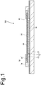
- FIG. 1 is a cut surface end view illustrating a first embodiment of a photoelectric conversion element of the present invention
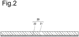
- FIG.2 is a cross-sectional view illustrating a counter substrate of FIG. 1
- FIG. 3 is a partial enlarged view of FIG. 1 .
- a photoelectric conversion element 100 has one photoelectric conversion cell 90.
- the photoelectric conversion cell 90 includes an electrode substrate 10; a counter substrate 20 facing the electrode substrate 10; a ring-shaped sealing portion bonding the electrode substrate 10 and the counter substrate 20; an electrolyte 40 disposed inside the sealing portion 30; an oxide semiconductor layer 50 provided on a surface of the electrode substrate 10 facing the counter substrate 20; and a dye (not shown) supported on the oxide semiconductor layer 50.
- the electrode substrate 10 includes a transparent substrate 13, a transparent conductive layer 14 provided on the transparent substrate 13 and a ring-shaped insulating part 15 on the transparent conductive layer 14 so as to surround the oxide semiconductor layer 50 and adhered to the sealing portion 30.
- the counter substrate 20 which includes a counter electrode, has a conductive substrate 21 which serves as a substrate and an electrode; and a catalyst layer 22 provided on the conductive substrate 21.
- the catalyst layer 22 is provided on a side of the conductive substrate 21 facing the electrode substrate 10.
- the sealing portion 30 includes a ring-shaped first resin sealing portion 70 adhered to the electrode substrate 10; and a ring-shaped second resin sealing portion 80 provided so as to sandwich the counter substrate 20 together with the first resin sealing portion 70.
- both the first resin sealing portion 70 and the second resin sealing portion 80 include a thermoplastic resin, and the second resin sealing portion 80 has a melting point higher than that of the first resin sealing portion 70.
- the first resin sealing portion 70 includes a first main body part 71 adhered to the electrode substrate 10; and a first protrusion part 72 provided on a side of the first main body part 71 facing the direction opposite to the electrode substrate 10.
- the first main body part 71 includes an insertion part 71a inserted between the electrode substrate 10 and the counter substrate 20; and a non-insertion part 71b which is not inserted between the electrode substrate 10 and the counter substrate 20.
- the first main body part 72 is provided on a side of the non-insertion part 71b of the first main body part 71 facing the direction opposite to the electrode substrate 10.
- the second resin sealing portion 80 includes a second main body part 81 provided on a side of the counter substrate 20 facing the direction opposite to the electrode substrate 10; and an intermediate part 82 between the second main body part 81 and the first protrusion part 72.
- the second main body part 81 of the second resin sealing portion 80 is adhered to the first protrusion part 72 via the intermediate part 82.
- the intermediate part 82 is adhered to the non-insertion part 71b of the first main body part 71.
- the sealing portion 30 includes the first resin sealing portion 70 having a melting point lower than that of the second resin sealing portion 80 and the first resin sealing portion 70 includes the insertion part 71a inserted between the electrode substrate 10 and the counter substrate 20.
- the photoelectric conversion element 100 When the photoelectric conversion element 100 is placed under a high temperature environment, and the cell space is pressurized in the photoelectric conversion cell 90, a force to push out the first resin sealing portion 70 of the sealing portion 30 acts on the first resin sealing portion 70 and a large shear stress is applied in a direction parallel to the interface between the electrode substrate 10 and the first sealing portion 70.
- the second main body part 81 of the second resin sealing portion 80 is provided on a side of the counter substrate 20 facing the direction opposite to the electrode substrate 10.
- the first resin sealing portion 70 does not include the first protrusion part 72 on a side of the first main body part 71 facing the direction opposite to the electrode substrate 10
- a shear stress applied to the interface between the counter substrate 20 and the second main body part 81 of the second resin sealing portion 80 is small.
- the difference between the shear stress applied to the interface between the electrode substrate 10 and the first resin sealing portion 70 and the shear stress applied to the interface between the counter substrate 20 and the second main body part 81 of the second resin sealing portion 80 becomes considerably large, and the first resin sealing portion 70 is easily peeled from the counter substrate 20.
- the second main body part 81 of the second resin sealing portion 80 is adhered to the first protrusion part 72 through the intermediate part 82.
- the second main body part 81 is simultaneously pulled outward through the intermediate part 82 of the second resin sealing portion 80 by the first protrusion part 72, and a stress to direct the second main body part 81 toward the outside is applied to the second main body part 81. That is, a shear stress applied to the interface between the counter substrate 20 and the second main body part 81 of the second resin sealing portion 80 is increased.
- the difference between the shear stress applied to the interface between the electrode substrate 10 and the first resin sealing portion 70 and the shear stress applied to the interface between counter substrate 20 and the second main body part 81 of the second resin sealing portion 80 can be sufficiently reduced and the first resin sealing portion 70 is less likely to be peeled from the counter substrate 20.
- the photoelectric conversion element 100 when the photoelectric conversion element 100 is placed in a low temperature environment, and the cell space is decompressed in the photoelectric conversion cell 90, a force to pull the first resin sealing portion 70 of the sealing portion 30 into the inside acts on the first resin sealing portion 70 and a large shear stress is applied in a direction parallel to the interface between the electrode substrate 10 and the first resin sealing portion 70.
- the second main body part 81 of the second resin sealing portion 80 is provided on a side of the counter substrate 20 facing the direction opposite to the electrode substrate 10.
- the first resin sealing portion 70 does not include the first protrusion part 72 on a side of the first main body part 71 facing the direction opposite to the electrode substrate 10, a shear stress applied to the interface between the counter substrate 20 and the second main body part 81 of the second resin sealing portion 80 is small.
- the difference between the shear stress applied to the interface between the electrode substrate 10 and the first resin sealing portion 70 and a shear stress applied to the interface between the counter substrate 20 and the second main body part 81 of the second resin sealing portion 80 becomes considerably large, and the first resin sealing portion 70 is easily peeled from the counter substrate 20.
- the second main body part 81 of the second resin sealing portion 80 is adhered to the first protrusion part 72 through the intermediate part 82.
- the second main body part 81 is simultaneously pushed inward through the intermediate part 82 of the second resin sealing portion 80 by the first protrusion part 72 and a stress to direct the second main body part 81 inward is applied.
- the difference between the shear stress applied to the interface between the electrode substrate 10 and the first resin sealing portion 70 and the shear stress applied to the interface between the counter substrate 20 and the second main body part 81 of the second resin sealing portion 80 can be sufficiently reduced and the first resin sealing portion 70 is less likely to be peeled from the counter substrate 20.
- the photoelectric conversion element 100 According to the photoelectric conversion element 100, the leakage of the electrolyte 40 caused by the peeling of the first resin sealing portion 70 from the electrode substrate 10 or the counter substrate 20 is sufficiently suppressed. Therefore, the photoelectric conversion element 100 can have excellent durability.
- the electrode substrate 10 the counter substrate 20, and the sealing portion 30, the electrolyte 40, the oxide semiconductor layer 50, and the dye will be described in detail.
- the electrode substrate 10 includes the transparent substrate 13; the transparent conductive layer 14 provided on the transparent substrate 13; and the ring-shaped insulating part 15 adhered to the sealing portion 30.
- the material constituting the transparent substrate 13 may be any transparent material, for example, and examples of such a transparent material include glass such as borosilicate glass, soda lime glass, glass which is made of soda lime and whose iron component is less than that of ordinary soda lime glass, and quartz glass; polyethylene terephthalate (PET), polyethylene naphthalate (PEN), polycarbonate (PC), and polyethersulfone (PES).
- the thickness of the transparent substrate 13 is appropriately determined depending on the size of the photoelectric conversion element 100 and is not particularly limited, but it may be set to the range of from 50 to 40000 ⁇ m, for example.
- the material constituting the transparent conductive layer 14 examples include a conductive metal oxide such as indium-doped-tin-oxide (ITO), tin oxide (SnO 2 ), and fluorine-doped-tin-oxide (FTO).
- the transparent conductive layer 14 may be constituted by a single layer or a laminate consisting of a plurality of layers which are constituted by different conductive metal oxides. It is preferable that the transparent conductive layer 14 be constituted by FTO since FTO exhibits high heat resistance and chemical resistance in a case in which the transparent conductive layer 14 is constituted by a single layer.
- the thickness of the transparent conductive layer 14 may be set to the range of from 0.01 to 2 ⁇ m, for example.
- the material constituting the insulating part 15 is not particularly limited as long as it is an insulating material, but, examples of the insulating material include, for example, an inorganic insulating material such as glass frit; a thermosetting resin such as a polyimide resin; and a thermoplastic resin. Among them, the inorganic insulating material such as glass frit or a thermosetting resin is preferably used. In this case, even if the sealing portion 30 has fluidity at a high temperature, the insulating part 15 is less likely to be fluidized even at a high temperature compared to the case where the insulating material is composed of a thermoplastic resin. Therefore, contact between the transparent conductive layer 14 of the electrode substrate 10 and the counter substrate 20 is sufficiently suppressed and short circuit between the transparent conductive layer 14 and the counter substrate 20 can be sufficiently suppressed.
- the thickness of the insulating part 15 is not particularly limited, the thickness is typically 10 to 30 ⁇ m, and preferably 15 to 25 ⁇ m.
- the counter substrate 20 includes the conductive substrate 21 which serves as a substrate and an electrode; and the catalyst layer 22 which is provided on a side of the conductive substrate 21 facing the electrode substrate 10 and promotes the catalyst reaction.
- the conductive substrate 21 is constituted by, for example, a corrosion-resistant metallic material such as titanium, nickel, platinum, molybdenum, tungsten, aluminum and stainless steel.
- the substrate and the electrode may be divided, and the conductive substrate 21 may be constituted by a stacked body in which a conductive layer made of a conductive oxide such as ITO, FTO or the like is formed as the electrode on the resin film, or may be a stacked body in which a conductive layer made of the conductive oxide such as ITO, FTO or the like is formed on glass.
- the thickness of the conductive substrate 21 is appropriately determined according to the size of the photoelectric conversion element 100 and is not particularly limited. However, the thickness may be set to 0.01 to 0.1 mm, for example.
- the catalyst layer 22 is made of a metal such as platinum, a carbon-based material, a conductive polymer or the like.
- the sealing portion 30 includes the first resin sealing portion 70 and the second resin sealing portion 80.
- thermoplastic resin contained in the first resin sealing portion 70 examples include a resin such as a modified polyolefin resin including an ionomer, an ethylene-vinyl acetate anhydride copolymer, an ethylene-methacrylic acid copolymer and an ethylene-vinyl alcohol copolymer; a vinyl alcohol polymer and the like.
- a resin such as a modified polyolefin resin including an ionomer, an ethylene-vinyl acetate anhydride copolymer, an ethylene-methacrylic acid copolymer and an ethylene-vinyl alcohol copolymer; a vinyl alcohol polymer and the like.
- the value of R represented by the following formula (3) is not particularly limited, but it is preferably 3.0 or more.
- R t 1 + t 2 ) / t 1 (In the above formula (3), t1 represents the thickness of the first main body part 71 and t2 represents the thickness of the first protrusion part 72).
- the photoelectric conversion element 100 can have more excellent durability.
- the value of R is more preferably 3.5 or more. However, the value of R is more preferably 21 or less.
- the thickness of the first main body part 71 of the first resin sealing portion 70 is not particularly limited, but, typically 10 to 100 ⁇ m, and preferably 20 to 50 ⁇ m.
- the thermoplastic resin contained in the second resin sealing portion 80 may be a resin which can give the second resin sealing portion 80 a melting point higher than that of the first resin sealing portion 70 and the same resin as the thermoplastic resin contained in the first resin sealing portion 70 can be used as the thermoplastic resin contained in the second resin sealing portion 80.
- ⁇ T which is the difference between the melting point T2 of the second resin sealing portion 80 and the melting point T1 of the first resin sealing portion 70 and is represented by the following formula (2), is not particularly limited as long as it is more than 0°C.
- ⁇ T is preferably 25°C or more. In this case, compared to a case where ⁇ T is less than 25°C, the peeling of the electrode substrate 10 or the counter substrate 20 from the first resin sealing portion 70 is more sufficiently suppressed.
- ⁇ T is preferably 35°C or more. However, ⁇ T is preferably 60°C or less.
- ⁇ ⁇ T T 2 ⁇ T 1
- the oxygen permeability of the second resin sealing portion 80 may be the same as or different from the oxygen permeability of the first resin sealing portion 70. However, the oxygen permeability of the second resin sealing portion 80 is preferably smaller than the oxygen permeability of the first resin sealing portion 70.
- the sealing portion 30 includes the second resin sealing portion 80 having an oxygen permeability smaller than that of the first resin sealing portion 70 in addition to the first resin sealing portion 70. For this reason, compared to a case where the sealing portion 30 does not include the second resin sealing portion 80, intrusion of oxygen into the electrolyte 40 through the sealing portion 30 is sufficiently suppressed, deterioration due to oxygen of the dye supported on the oxide semiconductor layer 50 is sufficiently suppressed, and the photoelectric conversion element 100 can have more excellent durability.
- the value of A which is the ratio of the oxygen permeability A1 of the first resin sealing portion 70 and the oxygen permeability A2 of the second resin sealing portion 80 and is expressed by the following formula (1) is not particularly limited, but is preferably 1,200 to 60,000. In this case, compared to a case where the value of A is out of the above range, intrusion of oxygen into the electrolyte 40 through the sealing portion 30 is sufficiently suppressed, deterioration due to oxygen of the dye supported on the oxide semiconductor layer 50 is more sufficiently suppressed by oxygen, and the photoelectric conversion element 100 can have more excellent durability.
- the value of A is more preferably 2,400 to 8,000.
- the oxygen permeability of the second resin sealing portion 80 is not particularly limited, but is typically 0.21 to 2.5 (cc/20 ⁇ m 2 ⁇ 24h/atm) and preferably from 0.5 to 2.0 (cc/20 ⁇ m 2 ⁇ 24h/atm).
- A A 1 / A 2
- the second resin sealing portion 80 a resin containing a vinyl alcohol unit is preferable.
- the resin containing a vinyl alcohol unit include an ethylene-vinyl alcohol copolymer and a vinyl alcohol polymer.
- the thickness of the second main body part 81 is not particularly limited, but, is typically 10 to 100 ⁇ m, and preferably 30 to 50 ⁇ m.
- the electrolyte 40 contains a redox pair and an organic solvent. It is possible to use acetonitrile, methoxy acetonitrile, 3-methoxy propionitrile, propionitrile, ethylene carbonate, propylene carbonate, diethyl carbonate, ⁇ -butyrolactone, valeronitrile or pivalonitrile as the organic solvent.
- redox pair examples include a redox couple such as a zinc complex, an iron complex, and a cobalt complex in addition to a redox pair containing a halogen atom such as iodide ion/polyiodide ion (for example, I - /I 3 - ), bromine ion/polybromide ion or the like.
- iodine ion/polyiodide ion can be formed by iodine (I 2 ) and a salt (an ionic liquid or a solid salt) containing iodide (I - ) as an anion.
- the ionic liquid having iodide as an anion only iodide may be added.
- a salt containing iodide (I - ) as an anion such as LiI, tetrabutylammonium iodide or the like may be added.
- the electrolyte 40 may use an ionic liquid instead of the organic solvent.
- a known iodide salt such as a pyridinium salt, an imidazolium salt, or a triazolium salt is used.
- an iodide salt for example, 1-hexyl-3-methylimidazolium iodide, 1-ethyl-3-propylimidazolium iodide, 1-ethyl-3-methylimidazolium iodide, 1,2-dimethyl-3-propylimidazolium iodide, 1-butyl-3-methylimidazolium iodide, or 1-methyl-3-propylimidazolium iodide is preferably used.
- the electrolyte 40 may use a mixture of the ionic liquid and the organic solvent instead of the organic solvent.
- an additive to the electrolyte 40.
- the additive include benzimidazole such as 1-methylbenzimidazole (NMB) or 1-butylbenzimidazole (NBB), 4-t-butylpyridine and guanidium thiocyanate. Among them, benzimidazole is preferable as the additive.
- a nanocomposite gel electrolyte which is a quasi-solid electrolyte obtained by kneading nanoparticles such as SiO 2 , TiO 2 , and carbon nanotubes with the electrolyte to form a gel-like form may be used, or an electrolyte gelled using an organic gelling agent such as polyvinylidene fluoride, a polyethylene oxide derivative or an amino acid derivative may also be used.
- the oxide semiconductor layer 50 is composed of oxide semiconductor particles.
- the oxide semiconductor particles are composed of, for example, titanium oxide (TiO 2 ), zinc oxide (ZnO), tungsten oxide (WO 3 ), niobium oxide (Nb 2 O 5 ), strontium titanate (SrTiO 3 ), tin oxide (SnO 2 ), indium oxide (In 3 O 3 ), zirconium oxide (ZrO 2 ), thallium oxide (Ta 2 O 5 ), lanthanum oxide (La 2 O 3 ), yttrium oxide (Y 2 O 3 ), holmium oxide (Ho 2 O 3 ), bismuth oxide (Bi 2 O 3 ), cerium oxide (CeO 2 ), aluminum oxide (Al 2 O 3 ), or two or more kinds of these.
- the thickness of the oxide semiconductor layer 50 may be set to from 0.1 to 100 ⁇ m, for example.
- the oxide semiconductor layer 50 is typically composed of an absorbing layer for absorbing light but may be composed of the absorbing layer and a reflective layer which returns the light transmitted through the absorbing layer to the absorbing layer by reflecting the light.
- a photosensitizing dye such as a ruthenium complex having a ligand including a bipyridine structure, a terpyridine structure, an organic dye such as porphyrin, eosin, rhodanine or merocyanine; and an organic-inorganic composite dye such as a halogenated lead-based perovskite crystal
- the ruthenium complex having a ligand including a bipyridine structure or a terpyridine structure is preferred.
- the photoelectric conversion element 100 is a dye-sensitized photoelectric conversion element.
- a conductive substrate obtained by forming the transparent conductive layer 14 on one transparent substrate 13 is prepared.
- a sputtering method As a method of forming the transparent conductive layer 14, a sputtering method, a vapor deposition method, a spray pyrolysis method (SPD) or a chemical vapor deposition (CVD) method can be used.
- a sputtering method As a method of forming the transparent conductive layer 14, a sputtering method, a vapor deposition method, a spray pyrolysis method (SPD) or a chemical vapor deposition (CVD) method can be used.
- SPD spray pyrolysis method
- CVD chemical vapor deposition
- a precursor of the oxide semiconductor layer 50 is formed on the transparent conductive layer 14.
- the precursor of the oxide semiconductor layer 50 can be formed by printing a paste for oxide semiconductor layer formation containing oxide semiconductor particles and then drying the paste.
- the paste for oxide semiconductor layer formation includes a resin such as polyethylene glycol, and a solvent such as terpineol in addition to the oxide semiconductor particles.
- a method of printing the paste for oxide semiconductor layer formation for example, a screen printing method, a doctor blade method, a bar coating method or the like can be used.
- the precursor of the oxide semiconductor layer 50 is fired to form the oxide semiconductor layer 50.
- the firing temperature varies depending on the kind of the oxide semiconductor particles, but is typically 350 to 600°C, and the firing time also varies depending on the kind of the oxide semiconductor particles, but is typically 1 to 5 hours.
- a precursor of the insulating part 15 is formed so as to surround the precursor of the oxide semiconductor layer 50.
- the precursor of the insulating part 15 can be formed, for example, by applying and drying a paste containing glass frit and drying the paste.
- the precursor of the insulating part 15 is fired to form the insulating part 15.
- the electrode substrate 10 on which the oxide semiconductor layer 50 and the insulating part 15 are formed is obtained.
- the first sealing resin sealing portion forming body can be obtained by preparing a first sealing resin film and forming one opening in the first sealing resin film, for example.
- the first sealing portion forming body is disposed along the insulating part 15 on the insulating part 15 so as to be adhered to the insulating part 15.
- adhesion of the first sealing portion forming body to the insulating part 15 can be performed by heating and melting the first sealing portion forming body, for example.
- the dye is supported on the oxide semiconductor layer 50 of the electrode substrate 10.
- the dye may be adsorbed on the oxide semiconductor layer 50 by immersing the electrode substrate 10 in a solution containing the dye, then washing out the extra dye with the solvent component of the above solution after making the dye adsorb on the oxide semiconductor layer 50 and performing drying.
- the electrolyte 40 is prepared. Then, the electrolyte 40 is disposed inside the ring-shaped sealing portion forming body fixed on the electrode substrate 10. Thus, a structure A is obtained.
- the counter substrate 20 is prepared.
- the counter substrate 20 can be obtained by forming the conductive catalyst layer 22 on the conductive substrate 21.
- a second resin sealing portion forming body having a melting point higher than that of the above-described first sealing portion forming body is prepared.
- the second resin sealing portion forming body can be obtained by preparing a second sealing resin film and forming one opening in the second sealing resin film, for example.
- the counter substrate 20 is arranged so as to block the opening of the first sealing portion forming body and then the first sealing portion forming body and the second sealing portion forming body are superimposed so as to sandwich the peripheral edge part of the counter substrate 20 by the first sealing portion forming body and the second sealing portion forming body. Then, the first sealing portion forming body and the second sealing portion forming body are adhered to the counter substrate 20.
- adhesion of the first sealing portion forming body and the second sealing portion forming body to the counter substrate 20 can be performed by heating and melting the first sealing portion forming body and the second sealing portion forming body, for example.
- a structure B is obtained.
- the structure A and the structure B are superimposed, the first sealing portion forming body of the structure A as well as the first sealing portion forming body and the second sealing portion forming body of the structure B are heated and melted while being pressurized. Then, the softening of the first sealing portion forming body starts, the outer peripheral edge part of the first sealing portion forming body facing each other rises up in a direction away from the electrode substrate 10 while spreading outside and are adhered to the second sealing portion forming body. Thus, the sealing portion 30 is formed.
- the photoelectric conversion element 100 is obtained.
- the photoelectric conversion element 100 includes one photoelectric conversion cell, but the photoelectric conversion element 100 may include a plurality of photoelectric conversion cells 90.
- the photoelectric conversion cell 90 includes the insulating part 15 between the sealing portion 30 and the electrode substrate 10, but the insulating part 15 is not necessarily required, and can be omitted.
- the second resin sealing portion 80 includes the second main body part 81 and the intermediate part 82, but the second resin sealing portion 80 may be composed of only the second main body part 81. That is, the second resin sealing portion 80 may not include the intermediate part 82. In this case, the second main body part 81 is directly adhered to the first protrusion part 72.
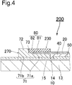
- a first resin sealing portion 270 may have a second protrusion part 73 having a thickness smaller than that of the first protrusion part 72 on the non-insertion part 71b of the first main body part 71 and may have an intermediate part 82 on the second protrusion part 73.
- the intermediate part 82 is adhered indirectly to the non-insertion part 71b of the first main body part 71 via the second protrusion part 73.
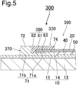
- a second resin sealing portion 380 may further include a turning part 83 which is connected to the intermediate part 82 and turns between the electrode substrate 10 and the counter substrate 20 in addition to the second main body part 81 and the intermediate part 82, and a first resin sealing portion 370 may further include a third protrusion part 74 on a side facing the direction opposite to the electrode substrate 10 in the insertion part 71a of the first main body part 71.
- the turning part 83 is preferably adhered to the third protrusion part 74.
- the turning part 83 of the second resin sealing portion 380 turns between the electrode substrate 10 and the counter substrate 20, and this turning part 83 is adhered to the third protrusion part 74.
- a force to push out the first resin sealing portion 370 of the sealing portion 30 to the outside is applied.
- a stress to direct the third protrusion part 74 to the outside is applied to the third protrusion part 74, a stress to direct the turning part 83 adhered to the third protrusion part 74 to the outside is also applied to the turning part 83.
- the stress applied to the turning part 83 is transmitted to the second main body part 81 of the second resin sealing portion 380, and a stress to direct the second main body part 81 to the outside is applied to the second main body part 81.
- the difference between a shear stress applied to the interface between the electrode substrate 10 and the first resin sealing portion 370 and a shear stress applied to the interface between the counter substrate 20 and the second main body part 81 of the second resin sealing portion 380 can be sufficiently reduced, and the first resin sealing portion 370 is less likely to be peeled from the counter substrate 20.
- the photoelectric conversion element 300 can have more excellent durability.
- the conductive substrate 21 and the catalyst layer 22 constitutes the counter substrate 20, but as in a photoelectric conversion cell 490 of a photoelectric conversion element 400 illustrated in FIG. 6 , as the counter substrate, an insulating substrate 420 may be used instead of the counter substrate 20.
- a structure 402 is disposed in a space between the insulating substrate 420, the sealing portion 30 and the electrode substrate 10.
- the structure 402 is provided on a surface of the electrode substrate 10 facing the insulating substrate 420.
- the structure 402 includes, in order from the electrode substrate 10 side, the oxide semiconductor layer 50, a porous insulating layer 403 and a counter electrode 401. Further, in the space, the electrolyte 40 is arranged.
- the electrolyte 40 is impregnated into the oxide semiconductor layer 50 and the porous insulating layer 403.
- the insulating substrate 420 for example, a glass substrate or a resin film can be used.
- the counter electrode 401 an electrode which is the same as the counter substrate 20 can be used.
- the counter electrode 401 may be composed of a porous single layer containing, for example, carbon.
- the porous insulating layer 403 is mainly used for preventing physical contact between the oxide semiconductor layer 50 and the insulating substrate 420 and impregnating the electrolyte 40 into the inside.
- the porous insulating layer 403 for example, a fired body of an oxide can be used.
- the porous insulating layer 403 is provided between the oxide semiconductor layer 50 and the counter electrode 401, but the porous insulating layer may be provided between the electrode substrate 10 and the counter electrode 401 so as to surround the oxide semiconductor layer 50.
- a conductive substrate was obtained by forming a transparent conductive layer made of FTO and having a thickness of 0.7 ⁇ m on a transparent substrate having a thickness of 2.2mm and composed of glass (trade name: TECa7, manufactured by Pilkington Group Limited) by a sputtering method.
- a precursor of an oxide semiconductor layer was formed on the transparent conductive layer.
- the precursor of the oxide semiconductor layer was formed by printing a titanium oxide paste (trade name "PST-21NR", manufactured by JGC Catalysts and Chemicals Ltd., the average particle diameter: 21 nm) with a thickness of 10 ⁇ m by screen printing first, and drying the paste.
- the precursor of the oxide semiconductor layer was fired at 500°C for 30 minutes, and an oxide semiconductor layer was formed on the transparent conductive layer.
- a glass insulating part was formed by printing a paste of low melting point glass frit (trade name: "PLFOC-837B", manufactured by Okuno Chemical Industries Co., Ltd.) such that the thickness after firing is 20 ⁇ m and the paste surround the oxide semiconductor layer, and then firing the paste at 500°C for 30 minutes.
- a paste of low melting point glass frit trade name: "PLFOC-837B", manufactured by Okuno Chemical Industries Co., Ltd.
- a resin film made of low density polyethylene (product name "BYNEL 4164", manufactured by DuPont, melting point: 127°C, oxygen permeability: 12,000(cc/20 ⁇ m 2 ⁇ 24h/atm)) was prepared, and a ring-shaped first sealing portion forming body was prepared by forming an opening in the resin film.
- the first sealing portion forming body was mounted on the glass insulating part, and then the first sealing portion forming body was welded to the glass insulating part by heat press.
- a dye was adsorbed on the oxide semiconductor layer by immersing the electrode substrate on which the first sealing portion forming body was formed in a dye solution for 16 hours. At this time, a Z907 dye solution of 0.2 mM was used as the dye solution.
- an electrolyte was disposed inside the first sealing portion forming body.
- an electrolyte obtained by dissolving iodine in a solvent comprising 3-methoxypropionitrile to have a concentration of 10mM.
- the structure A was obtained.
- a counter substrate was prepared by forming a catalyst layer made of platinum and having a thickness of 10 nm on a titanium foil having a thickness of 40 ⁇ m by a sputtering method. At this time, in both surfaces of the titanium foil, masking was applied to a peripheral edge part to weld a sealing portion forming body such that catalyst was not formed.
- a second sealing portion forming body for forming the second resin sealing portion was prepared.
- the ring-shaped second sealing portion forming body was prepared by preparing a resin film made of an ethylene vinyl alcohol copolymer (product name "EVELEF-E", manufactured by KURARAY CO., LTD., melting point: 165° C, oxygen permeability: 1.5 (cc/20 ⁇ m 2 ⁇ 24h)/atm)) and forming one opening in this resin film.
- the first sealing portion forming body and the second sealing portion forming body were superimposed so as to sandwich a peripheral part of the counter substrate by the first sealing portion forming body and the second sealing portion forming body. Then, the first sealing portion forming body and the second sealing portion forming body were adhered to the counter substrate by using a vacuum heat laminating method. Thus, a structure B was obtained.
- the structure A and the structure B were superimposed in a vacuum chamber having a degree of vacuum of 600 Pa, and the first sealing portion forming body of the structure A as well as the first sealing portion forming body and the second sealing portion forming body of the structure B were heated and melted while being pressurized by using a stepped hot mold obtained by providing a ring-shaped projection part on a main body part with the surface temperature of the projection part set to 200°C.
- the pressing was performed with press thrust set to about 1kN.
- softening of the first sealing portion forming body started, the outer peripheral edge part of the first sealing portion forming body facing each other rose up in a direction away from the electrode substrate while spreading outside, and were adhered to the second sealing portion forming body.
- the thickness t1 of the first main body part of the first resin sealing portion was 40 ⁇ m
- the thickness t2 of the first protrusion part was 80 ⁇ m
- R represented by the above-mentioned formula (3) was 3.0.
- a photoelectric conversion element was manufactured in the same manner as Example 1 except that a low-density polyethylene identical to that of the first sealing portion forming body was used in place of the ethylene vinyl alcohol copolymer.
- a photoelectric conversion element was manufactured in the same manner as Example 1 except that at the time of heating and melting the first sealing portion forming body of the structure A, as well as the first sealing portion forming body and the second sealing portion forming body of the structure B while pressurizing them, a sealing portion in which the first resin sealing portion did not include the first protrusion part in FIG.3 (that is, a sealing portion in which the value of R represented by the above-mentioned formula (3) was 1) was formed by changing the surface temperature of the projection part of the stepped hot mold from 200°C to 180°C and changing the press thrust from about 1kN to about 0.5kN.
- the photoelectric conversion element of the present invention can have excellent durability.
Landscapes
- Engineering & Computer Science (AREA)
- Power Engineering (AREA)
- Microelectronics & Electronic Packaging (AREA)
- Chemical & Material Sciences (AREA)
- Chemical Kinetics & Catalysis (AREA)
- Electrochemistry (AREA)
- Materials Engineering (AREA)
- Photovoltaic Devices (AREA)
- Hybrid Cells (AREA)
Abstract
Description
- The present invention relates to a photoelectric conversion element.
- As a photoelectric conversion element, a photoelectric conversion element using dyes attracts attention since it is inexpensive and can obtain high photoelectric conversion efficiency, and various developments on photoelectric conversion elements using dyes are performed.
- As the photoelectric conversion element using dyes, for example, a photoelectric conversion element described in the following patent document 1 is known. In the following patent document 1, disclosed is a photoelectric conversion element in which at least one photoelectric conversion cell includes: an electrode substrate; a counter substrate facing the electrode substrate; and a ring-shaped sealing portion bonding the electrode substrate and the counter substrate, and an electrolyte disposed inside the sealing portion. The following patent document 1 also discloses that the sealing portion includes a ring-shaped first resin sealing portion adhered to the electrode substrate, and a ring-shaped second resin sealing portion provided so as to sandwich the counter substrate together with the first resin sealing portion, and that the second resin sealing portion has a melting point higher than that of the first resin sealing portion. In this way, durability of the photoelectric conversion element is improved by providing a soft resin sealing portion between the electrode substrate and the counter substrate and relaxing the stress applied to an interface between the sealing portion and the electrode substrate or the counter substrate.
- Patent document 1: International Publication No.
2012/118028 - However, the photoelectric conversion element described in the above patent document 1 still has room for improvement in terms of durability.
- The present invention has been made in view of the above circumstances, an object of the present invention is to provide a photoelectric conversion element having excellent durability.
- In order to solve the above problems, the present invention is a photoelectric conversion element comprising at least one photoelectric conversion cell, wherein the photoelectric conversion cell includes: an electrode substrate; a counter substrate facing the electrode substrate; and a ring-shaped sealing portion bonding the electrode substrate and the counter substrate; and an electrolyte disposed inside the sealing portion, wherein the sealing portion includes: a ring-shaped first resin sealing portion bonded to the electrode substrate and containing a thermoplastic resin; and a ring-shaped second resin sealing portion provided so as to sandwich the counter substrate together with the first resin sealing portion and containing a thermoplastic resin, wherein the second resin sealing portion has a melting point higher than that of the first resin sealing portion, wherein the first resin sealing portion includes: a first main body part bonded to the electrode substrate; and a first protrusion part provided on a side of the first main body part facing the direction opposite to the electrode substrate, wherein the first main body part includes: an insertion part inserted between the electrode substrate and the counter substrate; and a non-insertion part which is not inserted between the electrode substrate and the counter substrate, wherein the first protrusion part is provided on the non-insertion part of the first main body part and the second resin sealing portion includes a second main body part provided on a side of the counter substrate facing the direction opposite to the electrode substrate and the second main body part of the second resin sealing portion is adhered to the first protrusion part.
- According to the photoelectric conversion element, when the photoelectric conversion element is placed under a high temperature environment, and a space between the counter substrate, the electrode substrate, and the sealing portion in the photoelectric conversion cell (hereinafter referred to as "cell space") is pressurized, the counter substrate and the electrode substrate try to separate from each other. At this time, the sealing portion includes the first resin sealing portion having a melting point lower than that of the second resin sealing portion and the first resin sealing portion includes the insertion part inserted between the electrode substrate and the counter substrate. For this reason, even if an excessive stress is about to be applied in a direction perpendicular to the interface between the counter substrate and the first resin sealing portion and the interface between the electrode substrate and the first resin sealing portion, the stress is relaxed by the first resin sealing portion. For this reason, application of an excessive stress to the interface between the first resin sealing portion and the counter substrate as well as the interface between the electrode substrate and the first resin sealing portion is sufficiently suppressed and the peeling of the electrode substrate or the counter substrate from the first resin sealing portion is sufficiently suppressed.
- In addition, when the photoelectric conversion element is placed under high temperature environment and the cell space is pressurized in the photoelectric conversion cell, a force pushing out the first resin sealing portion of the sealing portion to the outside acts on the first resin sealing portion, and a large shear stress is applied in a direction parallel to the interface between the electrode substrate and the first resin sealing portion. At this time, the second main body part of the second resin sealing portion is provided on a side of the counter substrate facing the direction opposite to the electrode substrate. For this reason, when it is assumed that the first resin sealing portion does not include the first protrusion part on a side of the first main body part facing the direction opposite to the electrode substrate, the shear stress applied to the interface between the counter substrate and the second main body part of the second resin sealing portion is small. As a result, the difference between the shear stress applied to the interface between the electrode substrate and the first resin sealing portion, and the shear stress applied to the interface between the counter substrate and the second main body part of the second resin sealing portion becomes considerably large, and the first resin sealing portion is easily peeled from the counter substrate. In contrast, when the first resin sealing portion has the first protrusion part on a side of the first main body part facing the direction opposite to the electrode substrate as in the present invention, the second main body part of the second resin sealing portion is adhered to the first protrusion part. For this reason, when a force pushing out the first resin sealing portion to the outside is applied and a stress to direct the first protrusion part to the outside is applied to the first protrusion part, the second main body part of the second resin sealing portion is simultaneously pulled outward by the first protrusion part, and a stress to direct the second main body part to the outside is applied. That is, the shear stress applied to the interface between the counter substrate and the second main body part of the second resin sealing portion increases. For this reason, the difference between the shear stress applied to the interface between the electrode substrate and the first resin sealing portion and the shear stress applied to the interface between the counter substrate and the second main body part of the second resin sealing portion can be sufficiently reduced, and the first resin sealing portion is less likely to be peeled from the counter substrate.
- On the other hand, when the photoelectric conversion element is placed under a low temperature environment and the cell space is decompressed in the photoelectric conversion cell, a force to pull the first resin sealing portion of the sealing portion into the inside acts on the first resin sealing portion, and a large shear stress is applied in a direction parallel to the interface between the electrode substrate and the first resin sealing portion. At this time, the second main body part of the second resin sealing portion is provided on a side of the counter substrate facing the direction opposite to the electrode substrate. Therefore, when it is assumed that the first resin sealing portion does not include the first protrusion part on a side of the first main body part facing the direction opposite to the electrode substrate, the shear stress applied to the interface between the counter substrate and the second main body part of the second resin sealing portion is small. As a result, the difference between the shear stress applied to the interface between the electrode substrate and the first resin sealing portion, and the shear stress applied to the interface between the counter substrate and the second main body part of the second resin sealing portion becomes considerably large, and the first resin sealing portion is easily peeled from the counter substrate. In contrast, in a case where the first resin sealing portion has the first protrusion part on a side of the first main body part facing the direction opposite to the electrode substrate as in the present invention, the second main body part of the second resin sealing portion is adhered to the first protrusion part. For this reason, when a force to pull the first resin sealing portion into the inside is applied and a stress to direct the first protrusion part toward the inside is applied to the first protrusion part, the second main body part of the second resin sealing portion is simultaneously pushed toward the inside by the first protrusion part, and a stress to direct the second main body part toward the inside is applied to the second main body part. For this reason, the difference between the shear stress applied to the interface between the electrode substrate and the first resin sealing portion and the shear stress applied to the interface between the counter substrate and the second main body part of the second resin sealing portion can be sufficiently reduced, and the first resin sealing portion is less likely to be peeled from the counter substrate.
- Thus, according to the photoelectric conversion element of the present invention, the leakage of the electrolyte caused by the peeling of the first resin sealing portion from the electrode substrate or the counter substrate is sufficiently suppressed. Therefore, the photoelectric conversion element of the present invention can have excellent durability.
- In the above-mentioned photoelectric conversion element, it is preferable that the photoelectric conversion cell further comprise an oxide semiconductor layer on the electrode substrate or the counter substrate, and a dye supported on the oxide semiconductor layer, and that the oxygen permeability of the second resin sealing portion be smaller than the oxygen permeability of the first resin sealing portion.
- In this case, the sealing portion includes the second resin sealing portion having an oxygen permeability smaller than that of the first resin sealing portion in addition to the first resin sealing portion. For this reason, compared to a case where the sealing portion does not include the second resin sealing portion, it is possible to sufficiently suppress the intrusion of oxygen into the electrolyte through the sealing portion, the deterioration due to oxygen of the dye supported on the oxide semiconductor layer is sufficiently suppressed, and the photoelectric conversion element can have more excellent durability.
- In the above-mentioned photoelectric conversion element, A represented by the following formula (1) is preferably 1,200 to 60,000.

- In this case, compared to a case where the value of A is out of the above range, the intrusion of oxygen into the electrolyte through the sealing portion is more sufficiently suppressed, the deterioration due to oxygen of the dye supported on the oxide semiconductor layer is more sufficiently suppressed, and the photoelectric conversion element can have more excellent durability.
- In the above-mentioned photoelectric conversion element, the second resin sealing portion preferably includes a resin containing a vinyl alcohol unit.
- In this case, since the oxygen permeability of the second resin sealing portion can be sufficiently reduced, the value of A represented by the above formula (1) can be easily adjusted.
- In the above-mentioned photoelectric conversion element, ΔT represented by the following formula (2) is preferably 25°C or higher.

- In this case, compared with a case where ΔT is less than 25°C, the peeling of the electrode substrate or the counter substrate from the first resin sealing portion is more sufficiently suppressed.
- In the above-mentioned photoelectric conversion element, it is preferable that the first resin sealing portion further includes a second protrusion part on a side facing the direction opposite to the electrode substrate in the insertion part of the main body part, and that the second resin sealing portion include a second main body part provided on a side of the counter substrate facing the direction opposite to the electrode substrate, and a turning part which is connected to the second main body part and turns between the electrode substrate and the counter substrate, and the turning part be adhered to the second protrusion part.
- In this case, the turning part of the second resin sealing portion turns between the electrode substrate and the counter substrate, and the turning part is adhered to the second protrusion part. Therefore, when the photoelectric conversion element is placed under a high temperature environment, and the cell space is pressurized in the photoelectric conversion cell, a force to push out the first resin sealing portion of the sealing portion to the outside is applied. At this time, when a stress to direct the second protrusion part to the outside is applied to the second protrusion part, a stress to direct the turning part adhered to the second protrusion part to the outside is also applied to the turning part. At this time, the stress applied to the turning part is transmitted to the second main body part of the second resin sealing portion, and a stress to direct the second main body part toward the outside is applied to the second main body part. For this reason, the difference between the shear stress applied to the interface between the electrode substrate and the first resin sealing portion and the shear stress applied to the interface between the counter substrate and the second main body part of the second resin sealing portion can be more sufficiently reduced, and the first resin sealing portion is less likely to be peeled from the counter substrate. As a result, the photoelectric conversion element can have more excellent durability.
- In the above-mentioned photoelectric conversion element, R represented by the following formula (3) is preferably 3.0 or more.

- In this case, compared to a case where R is less than 3.0, the photoelectric conversion element can have more excellent durability.
- According to the present invention, a photoelectric conversion element having excellent durability can be provided.
-
-
FIG. 1 is a cut surface end view illustrating a first embodiment of a photoelectric conversion element of the present invention; -
FIG. 2 is a cross-sectional view illustrating the counter substrate ofFIG. 1 ; -
FIG. 3 is a partially enlarged view ofFIG. 1 ; -
FIG. 4 is a cut surface end view illustrating a part of a second embodiment of the photoelectric conversion element of the present invention; -
FIG. 5 is a cut surface end view illustrating a part of a third embodiment of the photoelectric conversion element of the present invention; and -
FIG. 6 is a cut surface end view illustrating a fourth embodiment of the photoelectric conversion element of the present invention. - Hereinafter, an embodiment of the photoelectric conversion element of the present invention will be described in detail with reference to
FIGS. 1 to 3 .FIG. 1 is a cut surface end view illustrating a first embodiment of a photoelectric conversion element of the present invention;FIG.2 is a cross-sectional view illustrating a counter substrate ofFIG. 1 ; andFIG. 3 is a partial enlarged view ofFIG. 1 . - As illustrated in
FIG. 1 , aphotoelectric conversion element 100 has onephotoelectric conversion cell 90. Thephotoelectric conversion cell 90 includes anelectrode substrate 10; acounter substrate 20 facing theelectrode substrate 10; a ring-shaped sealing portion bonding theelectrode substrate 10 and thecounter substrate 20; anelectrolyte 40 disposed inside the sealingportion 30; anoxide semiconductor layer 50 provided on a surface of theelectrode substrate 10 facing thecounter substrate 20; and a dye (not shown) supported on theoxide semiconductor layer 50. - The
electrode substrate 10 includes atransparent substrate 13, a transparentconductive layer 14 provided on thetransparent substrate 13 and a ring-shaped insulatingpart 15 on the transparentconductive layer 14 so as to surround theoxide semiconductor layer 50 and adhered to the sealingportion 30. - As illustrated in
FIG. 2 , thecounter substrate 20, which includes a counter electrode, has aconductive substrate 21 which serves as a substrate and an electrode; and acatalyst layer 22 provided on theconductive substrate 21. Thecatalyst layer 22 is provided on a side of theconductive substrate 21 facing theelectrode substrate 10. - The sealing
portion 30 includes a ring-shaped firstresin sealing portion 70 adhered to theelectrode substrate 10; and a ring-shaped secondresin sealing portion 80 provided so as to sandwich thecounter substrate 20 together with the firstresin sealing portion 70. Herein, both the firstresin sealing portion 70 and the secondresin sealing portion 80 include a thermoplastic resin, and the secondresin sealing portion 80 has a melting point higher than that of the firstresin sealing portion 70. - As illustrated in
FIG.3 , the firstresin sealing portion 70 includes a firstmain body part 71 adhered to theelectrode substrate 10; and afirst protrusion part 72 provided on a side of the firstmain body part 71 facing the direction opposite to theelectrode substrate 10. The firstmain body part 71 includes aninsertion part 71a inserted between theelectrode substrate 10 and thecounter substrate 20; and anon-insertion part 71b which is not inserted between theelectrode substrate 10 and thecounter substrate 20. The firstmain body part 72 is provided on a side of thenon-insertion part 71b of the firstmain body part 71 facing the direction opposite to theelectrode substrate 10. - On the other hand, the second
resin sealing portion 80 includes a secondmain body part 81 provided on a side of thecounter substrate 20 facing the direction opposite to theelectrode substrate 10; and anintermediate part 82 between the secondmain body part 81 and thefirst protrusion part 72. - The second
main body part 81 of the secondresin sealing portion 80 is adhered to thefirst protrusion part 72 via theintermediate part 82. Theintermediate part 82 is adhered to thenon-insertion part 71b of the firstmain body part 71. - According to the
photoelectric conversion element 100, when thephotoelectric conversion element 100 is placed under a high temperature environment, and in the photoelectric conversion cell 90 a space (cell space) between thecounter substrate 20, theelectrode substrate 10 and the sealingportion 30 is pressurized, thecounter substrate 20 and theelectrode substrate 10 try to separate from each other. At this time, the sealingportion 30 includes the firstresin sealing portion 70 having a melting point lower than that of the secondresin sealing portion 80 and the firstresin sealing portion 70 includes theinsertion part 71a inserted between theelectrode substrate 10 and thecounter substrate 20. For this reason, even if an excessive stress is about to be applied in a direction perpendicular to the interface between thecounter substrate 20 and the firstresin sealing portion 70 as well as the interface between theelectrode substrate 10 and the firstresin sealing portion 70, the stress is relaxed by the firstresin sealing portion 70. Therefore, application of an excessive stress to the interface between the firstresin sealing portion 70 and thecounter substrate 20, as well as the interface between theelectrode substrate 10 and the firstresin sealing portion 70 is sufficiently suppressed and peeling of theelectrode substrate 10 or thecounter substrate 20 from the firstresin sealing portion 70 is sufficiently suppressed. - When the
photoelectric conversion element 100 is placed under a high temperature environment, and the cell space is pressurized in thephotoelectric conversion cell 90, a force to push out the firstresin sealing portion 70 of the sealingportion 30 acts on the firstresin sealing portion 70 and a large shear stress is applied in a direction parallel to the interface between theelectrode substrate 10 and thefirst sealing portion 70. At this time, the secondmain body part 81 of the secondresin sealing portion 80 is provided on a side of thecounter substrate 20 facing the direction opposite to theelectrode substrate 10. For this reason, when it is assumed that the firstresin sealing portion 70 does not include thefirst protrusion part 72 on a side of the firstmain body part 71 facing the direction opposite to theelectrode substrate 10, a shear stress applied to the interface between thecounter substrate 20 and the secondmain body part 81 of the secondresin sealing portion 80 is small. As a result, the difference between the shear stress applied to the interface between theelectrode substrate 10 and the firstresin sealing portion 70 and the shear stress applied to the interface between thecounter substrate 20 and the secondmain body part 81 of the secondresin sealing portion 80 becomes considerably large, and the firstresin sealing portion 70 is easily peeled from thecounter substrate 20. In contrast, in a case where the firstresin sealing portion 70 includes thefirst protrusion part 72 on a side of the firstmain body part 71 facing the direction opposite to theelectrode substrate 10 as in thephotoelectric conversion element 100, the secondmain body part 81 of the secondresin sealing portion 80 is adhered to thefirst protrusion part 72 through theintermediate part 82. For this reason, when a force to push out the firstresin sealing portion 70 to the outside is applied and a stress to direct thefirst protrusion part 72 toward the outside is applied to thefirst protrusion part 72, the secondmain body part 81 is simultaneously pulled outward through theintermediate part 82 of the secondresin sealing portion 80 by thefirst protrusion part 72, and a stress to direct the secondmain body part 81 toward the outside is applied to the secondmain body part 81. That is, a shear stress applied to the interface between thecounter substrate 20 and the secondmain body part 81 of the secondresin sealing portion 80 is increased. For this reason, the difference between the shear stress applied to the interface between theelectrode substrate 10 and the firstresin sealing portion 70 and the shear stress applied to the interface betweencounter substrate 20 and the secondmain body part 81 of the secondresin sealing portion 80 can be sufficiently reduced and the firstresin sealing portion 70 is less likely to be peeled from thecounter substrate 20. - On the other hand, when the
photoelectric conversion element 100 is placed in a low temperature environment, and the cell space is decompressed in thephotoelectric conversion cell 90, a force to pull the firstresin sealing portion 70 of the sealingportion 30 into the inside acts on the firstresin sealing portion 70 and a large shear stress is applied in a direction parallel to the interface between theelectrode substrate 10 and the firstresin sealing portion 70. At this time, the secondmain body part 81 of the secondresin sealing portion 80 is provided on a side of thecounter substrate 20 facing the direction opposite to theelectrode substrate 10. For this reason, when it is assumed that the firstresin sealing portion 70 does not include thefirst protrusion part 72 on a side of the firstmain body part 71 facing the direction opposite to theelectrode substrate 10, a shear stress applied to the interface between thecounter substrate 20 and the secondmain body part 81 of the secondresin sealing portion 80 is small. As a result, the difference between the shear stress applied to the interface between theelectrode substrate 10 and the firstresin sealing portion 70 and a shear stress applied to the interface between thecounter substrate 20 and the secondmain body part 81 of the secondresin sealing portion 80 becomes considerably large, and the firstresin sealing portion 70 is easily peeled from thecounter substrate 20. In contrast, in a case where the firstresin sealing portion 70 includes thefirst protrusion part 72 on a side of the firstmain body part 71 facing the direction opposite to theelectrode substrate 10 as in thephotoelectric conversion element 100, the secondmain body part 81 of the secondresin sealing portion 80 is adhered to thefirst protrusion part 72 through theintermediate part 82. For this reason, when a force to pull the firstresin sealing portion 70 inside is applied and a stress to direct thefirst protrusion part 72 inward is applied to thefirst protrusion part 72, the secondmain body part 81 is simultaneously pushed inward through theintermediate part 82 of the secondresin sealing portion 80 by thefirst protrusion part 72 and a stress to direct the secondmain body part 81 inward is applied. Therefore, the difference between the shear stress applied to the interface between theelectrode substrate 10 and the firstresin sealing portion 70 and the shear stress applied to the interface between thecounter substrate 20 and the secondmain body part 81 of the secondresin sealing portion 80 can be sufficiently reduced and the firstresin sealing portion 70 is less likely to be peeled from thecounter substrate 20. - Thus, according to the
photoelectric conversion element 100, the leakage of theelectrolyte 40 caused by the peeling of the firstresin sealing portion 70 from theelectrode substrate 10 or thecounter substrate 20 is sufficiently suppressed. Therefore, thephotoelectric conversion element 100 can have excellent durability. - Next, the
electrode substrate 10, thecounter substrate 20, and the sealingportion 30, theelectrolyte 40, theoxide semiconductor layer 50, and the dye will be described in detail. - As described above, the
electrode substrate 10 includes thetransparent substrate 13; the transparentconductive layer 14 provided on thetransparent substrate 13; and the ring-shaped insulatingpart 15 adhered to the sealingportion 30. - The material constituting the
transparent substrate 13 may be any transparent material, for example, and examples of such a transparent material include glass such as borosilicate glass, soda lime glass, glass which is made of soda lime and whose iron component is less than that of ordinary soda lime glass, and quartz glass; polyethylene terephthalate (PET), polyethylene naphthalate (PEN), polycarbonate (PC), and polyethersulfone (PES). The thickness of thetransparent substrate 13 is appropriately determined depending on the size of thephotoelectric conversion element 100 and is not particularly limited, but it may be set to the range of from 50 to 40000 µm, for example. - Examples of the material constituting the transparent
conductive layer 14 include a conductive metal oxide such as indium-doped-tin-oxide (ITO), tin oxide (SnO2), and fluorine-doped-tin-oxide (FTO). The transparentconductive layer 14 may be constituted by a single layer or a laminate consisting of a plurality of layers which are constituted by different conductive metal oxides. It is preferable that the transparentconductive layer 14 be constituted by FTO since FTO exhibits high heat resistance and chemical resistance in a case in which the transparentconductive layer 14 is constituted by a single layer. The thickness of the transparentconductive layer 14 may be set to the range of from 0.01 to 2 µm, for example. - The material constituting the insulating
part 15 is not particularly limited as long as it is an insulating material, but, examples of the insulating material include, for example, an inorganic insulating material such as glass frit; a thermosetting resin such as a polyimide resin; and a thermoplastic resin. Among them, the inorganic insulating material such as glass frit or a thermosetting resin is preferably used. In this case, even if the sealingportion 30 has fluidity at a high temperature, the insulatingpart 15 is less likely to be fluidized even at a high temperature compared to the case where the insulating material is composed of a thermoplastic resin. Therefore, contact between the transparentconductive layer 14 of theelectrode substrate 10 and thecounter substrate 20 is sufficiently suppressed and short circuit between the transparentconductive layer 14 and thecounter substrate 20 can be sufficiently suppressed. - Although the thickness of the insulating
part 15 is not particularly limited, the thickness is typically 10 to 30µm, and preferably 15 to 25µm. - As described above, the
counter substrate 20 includes theconductive substrate 21 which serves as a substrate and an electrode; and thecatalyst layer 22 which is provided on a side of theconductive substrate 21 facing theelectrode substrate 10 and promotes the catalyst reaction. - The
conductive substrate 21 is constituted by, for example, a corrosion-resistant metallic material such as titanium, nickel, platinum, molybdenum, tungsten, aluminum and stainless steel. Alternatively, the substrate and the electrode may be divided, and theconductive substrate 21 may be constituted by a stacked body in which a conductive layer made of a conductive oxide such as ITO, FTO or the like is formed as the electrode on the resin film, or may be a stacked body in which a conductive layer made of the conductive oxide such as ITO, FTO or the like is formed on glass. The thickness of theconductive substrate 21 is appropriately determined according to the size of thephotoelectric conversion element 100 and is not particularly limited. However, the thickness may be set to 0.01 to 0.1 mm, for example. - The
catalyst layer 22 is made of a metal such as platinum, a carbon-based material, a conductive polymer or the like. - The sealing
portion 30 includes the firstresin sealing portion 70 and the secondresin sealing portion 80. - Examples of the thermoplastic resin contained in the first
resin sealing portion 70 include a resin such as a modified polyolefin resin including an ionomer, an ethylene-vinyl acetate anhydride copolymer, an ethylene-methacrylic acid copolymer and an ethylene-vinyl alcohol copolymer; a vinyl alcohol polymer and the like. - In the first
resin sealing portion 70, the value of R represented by the following formula (3) is not particularly limited, but it is preferably 3.0 or more.
main body part 71 and t2 represents the thickness of the first protrusion part 72). - In this case, compared to a case where R is less than 3.0, the
photoelectric conversion element 100 can have more excellent durability. - The value of R is more preferably 3.5 or more. However, the value of R is more preferably 21 or less.
- The thickness of the first
main body part 71 of the firstresin sealing portion 70 is not particularly limited, but, typically 10 to 100µm, and preferably 20 to 50µm. - The thermoplastic resin contained in the second
resin sealing portion 80 may be a resin which can give the second resin sealing portion 80 a melting point higher than that of the firstresin sealing portion 70 and the same resin as the thermoplastic resin contained in the firstresin sealing portion 70 can be used as the thermoplastic resin contained in the secondresin sealing portion 80. - ΔT, which is the difference between the melting point T2 of the second
resin sealing portion 80 and the melting point T1 of the firstresin sealing portion 70 and is represented by the following formula (2), is not particularly limited as long as it is more than 0°C. However, ΔT is preferably 25°C or more. In this case, compared to a case where ΔT is less than 25°C, the peeling of theelectrode substrate 10 or thecounter substrate 20 from the firstresin sealing portion 70 is more sufficiently suppressed. ΔT is preferably 35°C or more. However, ΔT is preferably 60°C or less.
- The oxygen permeability of the second
resin sealing portion 80 may be the same as or different from the oxygen permeability of the firstresin sealing portion 70. However, the oxygen permeability of the secondresin sealing portion 80 is preferably smaller than the oxygen permeability of the firstresin sealing portion 70. In this case, the sealingportion 30 includes the secondresin sealing portion 80 having an oxygen permeability smaller than that of the firstresin sealing portion 70 in addition to the firstresin sealing portion 70. For this reason, compared to a case where the sealingportion 30 does not include the secondresin sealing portion 80, intrusion of oxygen into theelectrolyte 40 through the sealingportion 30 is sufficiently suppressed, deterioration due to oxygen of the dye supported on theoxide semiconductor layer 50 is sufficiently suppressed, and thephotoelectric conversion element 100 can have more excellent durability. - The value of A which is the ratio of the oxygen permeability A1 of the first
resin sealing portion 70 and the oxygen permeability A2 of the secondresin sealing portion 80 and is expressed by the following formula (1) is not particularly limited, but is preferably 1,200 to 60,000. In this case, compared to a case where the value of A is out of the above range, intrusion of oxygen into theelectrolyte 40 through the sealingportion 30 is sufficiently suppressed, deterioration due to oxygen of the dye supported on theoxide semiconductor layer 50 is more sufficiently suppressed by oxygen, and thephotoelectric conversion element 100 can have more excellent durability. The value of A is more preferably 2,400 to 8,000. The oxygen permeability of the secondresin sealing portion 80 is not particularly limited, but is typically 0.21 to 2.5 (cc/20 µm2·24h/atm) and preferably from 0.5 to 2.0 (cc/20 µm2·24h/atm).
- In addition, as the second
resin sealing portion 80, a resin containing a vinyl alcohol unit is preferable. In this case, since the oxygen permeability of the secondresin sealing portion 80 can be sufficiently reduced, the value of A represented by the above formula (1) can be easily adjusted. Examples of the resin containing a vinyl alcohol unit include an ethylene-vinyl alcohol copolymer and a vinyl alcohol polymer. - The thickness of the second
main body part 81 is not particularly limited, but, is typically 10 to 100µm, and preferably 30 to 50µm. - The
electrolyte 40 contains a redox pair and an organic solvent. It is possible to use acetonitrile, methoxy acetonitrile, 3-methoxy propionitrile, propionitrile, ethylene carbonate, propylene carbonate, diethyl carbonate, γ-butyrolactone, valeronitrile or pivalonitrile as the organic solvent. Examples of the redox pair include a redox couple such as a zinc complex, an iron complex, and a cobalt complex in addition to a redox pair containing a halogen atom such as iodide ion/polyiodide ion (for example, I-/I3 -), bromine ion/polybromide ion or the like. In addition, iodine ion/polyiodide ion can be formed by iodine (I2) and a salt (an ionic liquid or a solid salt) containing iodide (I-) as an anion. In a case of using the ionic liquid having iodide as an anion, only iodide may be added. In a case of using an organic solvent or an ionic liquid other than iodide as an anion, a salt containing iodide (I-) as an anion such as LiI, tetrabutylammonium iodide or the like may be added. In addition, theelectrolyte 40 may use an ionic liquid instead of the organic solvent. As the ionic liquid, for example, a known iodide salt such as a pyridinium salt, an imidazolium salt, or a triazolium salt is used. As such an iodide salt, for example, 1-hexyl-3-methylimidazolium iodide, 1-ethyl-3-propylimidazolium iodide, 1-ethyl-3-methylimidazolium iodide, 1,2-dimethyl-3-propylimidazolium iodide, 1-butyl-3-methylimidazolium iodide, or 1-methyl-3-propylimidazolium iodide is preferably used. - In addition, the
electrolyte 40 may use a mixture of the ionic liquid and the organic solvent instead of the organic solvent. - In addition, it is possible to add an additive to the
electrolyte 40. Examples of the additive include benzimidazole such as 1-methylbenzimidazole (NMB) or 1-butylbenzimidazole (NBB), 4-t-butylpyridine and guanidium thiocyanate. Among them, benzimidazole is preferable as the additive. - Moreover, as the
electrolyte 40, a nanocomposite gel electrolyte which is a quasi-solid electrolyte obtained by kneading nanoparticles such as SiO2, TiO2, and carbon nanotubes with the electrolyte to form a gel-like form may be used, or an electrolyte gelled using an organic gelling agent such as polyvinylidene fluoride, a polyethylene oxide derivative or an amino acid derivative may also be used. - The
oxide semiconductor layer 50 is composed of oxide semiconductor particles. The oxide semiconductor particles are composed of, for example, titanium oxide (TiO2), zinc oxide (ZnO), tungsten oxide (WO3), niobium oxide (Nb2O5), strontium titanate (SrTiO3), tin oxide (SnO2), indium oxide (In3O3), zirconium oxide (ZrO2), thallium oxide (Ta2O5), lanthanum oxide (La2O3), yttrium oxide (Y2O3), holmium oxide (Ho2O3), bismuth oxide (Bi2O3), cerium oxide (CeO2), aluminum oxide (Al2O3), or two or more kinds of these. The thickness of theoxide semiconductor layer 50 may be set to from 0.1 to 100 µm, for example. - The
oxide semiconductor layer 50 is typically composed of an absorbing layer for absorbing light but may be composed of the absorbing layer and a reflective layer which returns the light transmitted through the absorbing layer to the absorbing layer by reflecting the light. - As the dye, for example, a photosensitizing dye such as a ruthenium complex having a ligand including a bipyridine structure, a terpyridine structure, an organic dye such as porphyrin, eosin, rhodanine or merocyanine; and an organic-inorganic composite dye such as a halogenated lead-based perovskite crystal may be exemplified. As the halogenated lead-based perovskite, for example, CH3NH3PbX3 (X = Cl, Br, I) is used. Among the above-mentioned dyes, the ruthenium complex having a ligand including a bipyridine structure or a terpyridine structure is preferred. In this case, it is possible to more improve the photoelectric conversion characteristic of the
photoelectric conversion element 100. In addition, in a case where a photosensitizing dye is used as the dye, thephotoelectric conversion element 100 is a dye-sensitized photoelectric conversion element. - Next, a method of manufacturing the
photoelectric conversion element 100 will be described. - First, a conductive substrate obtained by forming the transparent
conductive layer 14 on onetransparent substrate 13 is prepared. - As a method of forming the transparent
conductive layer 14, a sputtering method, a vapor deposition method, a spray pyrolysis method (SPD) or a chemical vapor deposition (CVD) method can be used. - Further, a precursor of the
oxide semiconductor layer 50 is formed on the transparentconductive layer 14. - The precursor of the
oxide semiconductor layer 50 can be formed by printing a paste for oxide semiconductor layer formation containing oxide semiconductor particles and then drying the paste. - The paste for oxide semiconductor layer formation includes a resin such as polyethylene glycol, and a solvent such as terpineol in addition to the oxide semiconductor particles.
- As a method of printing the paste for oxide semiconductor layer formation, for example, a screen printing method, a doctor blade method, a bar coating method or the like can be used.
- Then, the precursor of the
oxide semiconductor layer 50 is fired to form theoxide semiconductor layer 50. - The firing temperature varies depending on the kind of the oxide semiconductor particles, but is typically 350 to 600°C, and the firing time also varies depending on the kind of the oxide semiconductor particles, but is typically 1 to 5 hours.
- Next, a precursor of the insulating
part 15 is formed so as to surround the precursor of theoxide semiconductor layer 50. - The precursor of the insulating
part 15 can be formed, for example, by applying and drying a paste containing glass frit and drying the paste. - Then, the precursor of the insulating
part 15 is fired to form the insulatingpart 15. - Thus, the
electrode substrate 10 on which theoxide semiconductor layer 50 and the insulatingpart 15 are formed is obtained. - Next, a ring-shaped first sealing portion forming body for forming the first
resin sealing portion 70 is prepared. The first sealing resin sealing portion forming body can be obtained by preparing a first sealing resin film and forming one opening in the first sealing resin film, for example. - Then, the first sealing portion forming body is disposed along the insulating
part 15 on the insulatingpart 15 so as to be adhered to the insulatingpart 15. At this time, adhesion of the first sealing portion forming body to the insulatingpart 15 can be performed by heating and melting the first sealing portion forming body, for example. - Next, the dye is supported on the
oxide semiconductor layer 50 of theelectrode substrate 10. To perform this, the dye may be adsorbed on theoxide semiconductor layer 50 by immersing theelectrode substrate 10 in a solution containing the dye, then washing out the extra dye with the solvent component of the above solution after making the dye adsorb on theoxide semiconductor layer 50 and performing drying. However, it is also possible to support the dye on theoxide semiconductor layer 50 by coating a solution containing the dye on theoxide semiconductor layer 50 and then drying to adsorb the dye on theoxide semiconductor layer 50. - Next, the
electrolyte 40 is prepared. Then, theelectrolyte 40 is disposed inside the ring-shaped sealing portion forming body fixed on theelectrode substrate 10. Thus, a structure A is obtained. - Next, the
counter substrate 20 is prepared. - As described above, the
counter substrate 20 can be obtained by forming theconductive catalyst layer 22 on theconductive substrate 21. - Next, another first sealing portion forming body described above is prepared.
- On the other hand, a second resin sealing portion forming body having a melting point higher than that of the above-described first sealing portion forming body is prepared. The second resin sealing portion forming body can be obtained by preparing a second sealing resin film and forming one opening in the second sealing resin film, for example.
- The, the
counter substrate 20 is arranged so as to block the opening of the first sealing portion forming body and then the first sealing portion forming body and the second sealing portion forming body are superimposed so as to sandwich the peripheral edge part of thecounter substrate 20 by the first sealing portion forming body and the second sealing portion forming body. Then, the first sealing portion forming body and the second sealing portion forming body are adhered to thecounter substrate 20. In addition, adhesion of the first sealing portion forming body and the second sealing portion forming body to thecounter substrate 20 can be performed by heating and melting the first sealing portion forming body and the second sealing portion forming body, for example. Thus, a structure B is obtained. - Next, the structure A and the structure B are superimposed, the first sealing portion forming body of the structure A as well as the first sealing portion forming body and the second sealing portion forming body of the structure B are heated and melted while being pressurized. Then, the softening of the first sealing portion forming body starts, the outer peripheral edge part of the first sealing portion forming body facing each other rises up in a direction away from the
electrode substrate 10 while spreading outside and are adhered to the second sealing portion forming body. Thus, the sealingportion 30 is formed. - Thus, the
photoelectric conversion element 100 is obtained. - The present invention is not limited to the above embodiment. For example, in the above embodiment, the
photoelectric conversion element 100 includes one photoelectric conversion cell, but thephotoelectric conversion element 100 may include a plurality ofphotoelectric conversion cells 90. - In addition, in the above embodiment, the
photoelectric conversion cell 90 includes the insulatingpart 15 between the sealingportion 30 and theelectrode substrate 10, but the insulatingpart 15 is not necessarily required, and can be omitted. - Furthermore, in the above embodiment, the second
resin sealing portion 80 includes the secondmain body part 81 and theintermediate part 82, but the secondresin sealing portion 80 may be composed of only the secondmain body part 81. That is, the secondresin sealing portion 80 may not include theintermediate part 82. In this case, the secondmain body part 81 is directly adhered to thefirst protrusion part 72. - Further, in the above embodiment, the
intermediate part 82 of the secondresin sealing portion 80 is provided directly on thenon-insertion part 71b of the firstmain body part 71 of the firstresin sealing portion 70, but as in a sealingportion 230 of aphotoelectric conversion element 200 illustrated inFIG.4 , a firstresin sealing portion 270 may have asecond protrusion part 73 having a thickness smaller than that of thefirst protrusion part 72 on thenon-insertion part 71b of the firstmain body part 71 and may have anintermediate part 82 on thesecond protrusion part 73. In this case, theintermediate part 82 is adhered indirectly to thenon-insertion part 71b of the firstmain body part 71 via thesecond protrusion part 73. - Further, in the above embodiment, the second
resin sealing portion 80 includes the secondmain body part 81 and theintermediate part 82, and the firstresin sealing portion 70 includes the firstmain body part 71 and thefirst protrusion part 72, but as in a sealingportion 330 of aphotoelectric conversion element 300 illustrated inFIG.5 , a secondresin sealing portion 380 may further include a turningpart 83 which is connected to theintermediate part 82 and turns between theelectrode substrate 10 and thecounter substrate 20 in addition to the secondmain body part 81 and theintermediate part 82, and a firstresin sealing portion 370 may further include athird protrusion part 74 on a side facing the direction opposite to theelectrode substrate 10 in theinsertion part 71a of the firstmain body part 71. Herein, the turningpart 83 is preferably adhered to thethird protrusion part 74. - In this case, the turning
part 83 of the secondresin sealing portion 380 turns between theelectrode substrate 10 and thecounter substrate 20, and this turningpart 83 is adhered to thethird protrusion part 74. For this reason, when thephotoelectric conversion element 300 is placed under a high temperature environment and the cell space is pressurized in aphotoelectric conversion cell 390, a force to push out the firstresin sealing portion 370 of the sealingportion 30 to the outside is applied. At this time, when a stress to direct thethird protrusion part 74 to the outside is applied to thethird protrusion part 74, a stress to direct the turningpart 83 adhered to thethird protrusion part 74 to the outside is also applied to the turningpart 83. At this time, the stress applied to the turningpart 83 is transmitted to the secondmain body part 81 of the secondresin sealing portion 380, and a stress to direct the secondmain body part 81 to the outside is applied to the secondmain body part 81. For this reason, the difference between a shear stress applied to the interface between theelectrode substrate 10 and the firstresin sealing portion 370 and a shear stress applied to the interface between thecounter substrate 20 and the secondmain body part 81 of the secondresin sealing portion 380 can be sufficiently reduced, and the firstresin sealing portion 370 is less likely to be peeled from thecounter substrate 20. As a result, thephotoelectric conversion element 300 can have more excellent durability. - Furthermore, in the above embodiment, the
conductive substrate 21 and thecatalyst layer 22 constitutes thecounter substrate 20, but as in aphotoelectric conversion cell 490 of aphotoelectric conversion element 400 illustrated inFIG. 6 , as the counter substrate, an insulatingsubstrate 420 may be used instead of thecounter substrate 20. In this case, astructure 402 is disposed in a space between the insulatingsubstrate 420, the sealingportion 30 and theelectrode substrate 10. Thestructure 402 is provided on a surface of theelectrode substrate 10 facing the insulatingsubstrate 420. Thestructure 402 includes, in order from theelectrode substrate 10 side, theoxide semiconductor layer 50, a porous insulatinglayer 403 and acounter electrode 401. Further, in the space, theelectrolyte 40 is arranged. Theelectrolyte 40 is impregnated into theoxide semiconductor layer 50 and the porous insulatinglayer 403. Herein, as the insulatingsubstrate 420, for example, a glass substrate or a resin film can be used. As thecounter electrode 401, an electrode which is the same as thecounter substrate 20 can be used. Alternatively, thecounter electrode 401 may be composed of a porous single layer containing, for example, carbon. The porousinsulating layer 403 is mainly used for preventing physical contact between theoxide semiconductor layer 50 and the insulatingsubstrate 420 and impregnating theelectrolyte 40 into the inside. As such the porous insulatinglayer 403, for example, a fired body of an oxide can be used. In addition, in thephotoelectric conversion element 400 illustrated inFIG. 6 , only onestructure 402 is provided in the space between the sealingportion 30, theelectrode substrate 10 and the insulatingsubstrate 420, but a plurality of thestructures 402 may be provided. In addition, the porous insulatinglayer 403 is provided between theoxide semiconductor layer 50 and thecounter electrode 401, but the porous insulating layer may be provided between theelectrode substrate 10 and thecounter electrode 401 so as to surround theoxide semiconductor layer 50. With this structure as well, it is possible to prevent physical contact between theoxide semiconductor layer 50 and thecounter electrode 401. - Hereinafter, the content of the present invention will be described more specifically with reference to examples, but the present invention is not limited to the following examples.
- First, a conductive substrate was obtained by forming a transparent conductive layer made of FTO and having a thickness of 0.7µm on a transparent substrate having a thickness of 2.2mm and composed of glass (trade name: TECa7, manufactured by Pilkington Group Limited) by a sputtering method.
- Next, a precursor of an oxide semiconductor layer was formed on the transparent conductive layer. Specifically, the precursor of the oxide semiconductor layer was formed by printing a titanium oxide paste (trade name "PST-21NR", manufactured by JGC Catalysts and Chemicals Ltd., the average particle diameter: 21 nm) with a thickness of 10µm by screen printing first, and drying the paste.
- Next, the precursor of the oxide semiconductor layer was fired at 500°C for 30 minutes, and an oxide semiconductor layer was formed on the transparent conductive layer.
- Next, a glass insulating part was formed by printing a paste of low melting point glass frit (trade name: "PLFOC-837B", manufactured by Okuno Chemical Industries Co., Ltd.) such that the thickness after firing is 20µm and the paste surround the oxide semiconductor layer, and then firing the paste at 500°C for 30 minutes. Thus, an electrode substrate on which the oxide semiconductor layer and the glass insulating part were formed was obtained.
- Next, a resin film made of low density polyethylene (product name "BYNEL 4164", manufactured by DuPont, melting point: 127°C, oxygen permeability: 12,000(cc/20µm2·24h/atm)) was prepared, and a ring-shaped first sealing portion forming body was prepared by forming an opening in the resin film.
- Then, the first sealing portion forming body was mounted on the glass insulating part, and then the first sealing portion forming body was welded to the glass insulating part by heat press.
- Next, a dye was adsorbed on the oxide semiconductor layer by immersing the electrode substrate on which the first sealing portion forming body was formed in a dye solution for 16 hours. At this time, a Z907 dye solution of 0.2 mM was used as the dye solution.
- Next, an electrolyte was disposed inside the first sealing portion forming body. As the electrolyte, an electrolyte obtained by dissolving iodine in a solvent comprising 3-methoxypropionitrile to have a concentration of 10mM. Thus, the structure A was obtained.
- Next, a counter substrate was prepared by forming a catalyst layer made of platinum and having a thickness of 10 nm on a titanium foil having a thickness of 40µm by a sputtering method. At this time, in both surfaces of the titanium foil, masking was applied to a peripheral edge part to weld a sealing portion forming body such that catalyst was not formed.
- Next, another ring-shaped first sealing portion forming body described above was prepared. On the other hand, a second sealing portion forming body for forming the second resin sealing portion was prepared. The ring-shaped second sealing portion forming body was prepared by preparing a resin film made of an ethylene vinyl alcohol copolymer (product name "EVELEF-E", manufactured by KURARAY CO., LTD., melting point: 165° C, oxygen permeability: 1.5 (cc/20µm2·24h)/atm)) and forming one opening in this resin film.
- Then, after the counter substrate was arranged so as to block the opening of the first sealing portion forming body, the first sealing portion forming body and the second sealing portion forming body were superimposed so as to sandwich a peripheral part of the counter substrate by the first sealing portion forming body and the second sealing portion forming body. Then, the first sealing portion forming body and the second sealing portion forming body were adhered to the counter substrate by using a vacuum heat laminating method. Thus, a structure B was obtained.
- Then, the structure A and the structure B were superimposed in a vacuum chamber having a degree of vacuum of 600 Pa, and the first sealing portion forming body of the structure A as well as the first sealing portion forming body and the second sealing portion forming body of the structure B were heated and melted while being pressurized by using a stepped hot mold obtained by providing a ring-shaped projection part on a main body part with the surface temperature of the projection part set to 200°C. At this time, the pressing was performed with press thrust set to about 1kN. As a result, softening of the first sealing portion forming body started, the outer peripheral edge part of the first sealing portion forming body facing each other rose up in a direction away from the electrode substrate while spreading outside, and were adhered to the second sealing portion forming body. In this way, a sealing portion having a shape as illustrated in
FIG.3 was formed. At this time, the thickness t1 of the first main body part of the first resin sealing portion was 40µm, the thickness t2 of the first protrusion part was 80µm, and R represented by the above-mentioned formula (3) was 3.0. - Thus, a photoelectric conversion element composed of one photoelectric conversion cell was obtained.
- A photoelectric conversion element was manufactured in the same manner as Example 1 except that a low-density polyethylene identical to that of the first sealing portion forming body was used in place of the ethylene vinyl alcohol copolymer.
- A photoelectric conversion element was manufactured in the same manner as Example 1 except that at the time of heating and melting the first sealing portion forming body of the structure A, as well as the first sealing portion forming body and the second sealing portion forming body of the structure B while pressurizing them, a sealing portion in which the first resin sealing portion did not include the first protrusion part in
FIG.3 (that is, a sealing portion in which the value of R represented by the above-mentioned formula (3) was 1) was formed by changing the surface temperature of the projection part of the stepped hot mold from 200°C to 180°C and changing the press thrust from about 1kN to about 0.5kN. - For the photoelectric conversion elements of Example 1, Comparative Example 1 and Comparative Example 2 obtained as described above, heat cycle test was performed, and measurements of the IV curves was performed under an illuminance of 200 lux with a white LED used as a light source before and after the heat cycle test. The output retention rates were calculated on the basis of the output obtained from the IV curves and the following formula. The results are illustrated in Table 1.

- In addition, 200 times of heat cycle tests were performed according to JIS C8917, with a heat cycle of lowering temperature to -40°C and then raising temperature to 90°C as one cycle.
[Table 1] Presence or Absence of Second Resin Sealing Portion Presence or Absence of First Protrusion Part in First Resin Sealing Portion Thickness t1 of First Main Body Part (µm) Thickness t2 of First Protrusion Part (µm) R(=(t1+t2)/t1) Durability Output Retention Rate (%) Example 1 Present Present 40 80 3 95.2 Comparative Example 1 Absent - - - - 92.4 Comparative Example 2 Present Absent 40 0 1 89.1 - From the results illustrated in Table 1, it was found that the output retention rate of the photoelectric conversion element of Example 1 was greater than the output retention rates of Comparative Examples 1 and 2.
- From this, it was confirmed that the photoelectric conversion element of the present invention can have excellent durability.
-
- 10
- Electrode substrate
- 20
- Counter substrate
- 30
- Sealing portion
- 40
- Electrolyte
- 50
- Oxide semiconductor layer
- 70
- First resin sealing portion
- 71
- First main body part
- 71a
- Insertion part
- 71b
- Non-insertion part
- 72
- First protrusion part
- 73
- Second protrusion part
- 80
- Second resin sealing portion
- 81
- Second main body part
- 83
- Turning part
- 90, 390, 490
- Photoelectric conversion cell
- 100,200,300, 400
- Photoelectric conversion element
- 420
- Insulating substrate (counter substrate)
Claims (7)
- A photoelectric conversion element comprising at least one photoelectric conversion cell, wherein the photoelectric conversion cell comprises
an electrode substrate;
a counter substrate facing the electrode substrate;
a ring-shaped sealing portion bonding the electrode substrate and the counter substrate; and
an electrolyte disposed inside the sealing portion,
wherein the sealing portion includes:a ring-shaped first resin sealing portion adhered to the electrode substrate and containing a thermoplastic resin; anda ring-shaped second resin sealing portion provided so as to sandwich the counter substrate together with the first resin sealing portion and containing a thermoplastic resin,wherein the second resin sealing portion has a melting point higher than that of the first resin sealing portion,wherein the first resin sealing portion includes:a first main body part adhered to the electrode substrate; anda first protrusion part provided on a side of the first main body part facing the direction opposite to the electrode substrate,wherein the first main body part includes:an insertion part inserted between the electrode substrate and the counter substrate; anda non-insertion part which is not inserted between the electrode substrate and the counter substrate,wherein the first protrusion part is provided in the non-insertion part of the first main body part,the second resin sealing portion comprises a second main body part provided on a side of the counter substrate facing the direction opposite to the electrode substrate, andthe second main body part of the second resin sealing portion is adhered to the first protrusion part. - The photoelectric conversion element according to claim 1, wherein the photoelectric conversion element further comprises an oxide semiconductor layer on the electrode substrate or the counter substrate; and a dye supported on the oxide semiconductor layer,
wherein the oxygen permeability of the second resin sealing portion is smaller than the oxygen permeability of the first resin sealing portion. - The photoelectric conversion element according to claim 2, wherein A represented by the following formula (1) is 1,200 to 60,000.

- The photoelectric conversion element according to claim 2 or 3, wherein the second resin sealing portion includes a resin containing a vinyl alcohol unit.
- The photoelectric conversion element according to any one of claims 1 to 4, wherein ΔT represented by the following formula (2) is 25°C or more.

- The photoelectric conversion element according to any one of claims 1 to 5, wherein the first resin sealing portion further comprises a second protrusion part on a side facing the direction opposite to the electrode substrate in the insertion part of the first main body part,
the second resin sealing portion further comprises a turning part which is connected to the second main body part and turns between the electrode substrate and the counter substrate, and
the turning part is adhered to the second protrusion part. - The photoelectric conversion element according to any one of claims 1 to 6, wherein R represented by the following formula (3) is 3.0 or more.

Applications Claiming Priority (2)
| Application Number | Priority Date | Filing Date | Title |
|---|---|---|---|
| JP2016165514A JP6259878B1 (en) | 2016-08-26 | 2016-08-26 | Photoelectric conversion element |
| PCT/JP2017/030212 WO2018038185A1 (en) | 2016-08-26 | 2017-08-23 | Photoelectric conversion element |
Publications (2)
| Publication Number | Publication Date |
|---|---|
| EP3506327A1 true EP3506327A1 (en) | 2019-07-03 |
| EP3506327A4 EP3506327A4 (en) | 2020-05-06 |
Family
ID=60940283
Family Applications (1)
| Application Number | Title | Priority Date | Filing Date |
|---|---|---|---|
| EP17843663.0A Withdrawn EP3506327A4 (en) | 2016-08-26 | 2017-08-23 | Photoelectric conversion element |
Country Status (5)
| Country | Link |
|---|---|
| US (1) | US20190180947A1 (en) |
| EP (1) | EP3506327A4 (en) |
| JP (1) | JP6259878B1 (en) |
| CN (1) | CN109155201A (en) |
| WO (1) | WO2018038185A1 (en) |
Families Citing this family (1)
| Publication number | Priority date | Publication date | Assignee | Title |
|---|---|---|---|---|
| JP6439035B1 (en) * | 2017-12-28 | 2018-12-19 | 株式会社フジクラ | Photoelectric conversion element |
Family Cites Families (7)
| Publication number | Priority date | Publication date | Assignee | Title |
|---|---|---|---|---|
| JP2002158146A (en) * | 2000-09-11 | 2002-05-31 | Nec Corp | Electric double-layer capacitor |
| JP5572307B2 (en) * | 2007-12-28 | 2014-08-13 | 株式会社半導体エネルギー研究所 | Method for manufacturing photoelectric conversion device |
| JP5320405B2 (en) * | 2008-10-30 | 2013-10-23 | 株式会社フジクラ | Photoelectric conversion device |
| JP4759646B1 (en) * | 2010-04-02 | 2011-08-31 | 株式会社フジクラ | Electronic device and manufacturing method thereof |
| JP5597304B2 (en) * | 2011-03-02 | 2014-10-01 | 株式会社フジクラ | Dye-sensitized solar cell module |
| JP5410628B1 (en) * | 2013-03-30 | 2014-02-05 | 株式会社フジクラ | Dye-sensitized solar cell element |
| JP5897741B1 (en) * | 2015-02-04 | 2016-03-30 | 株式会社フジクラ | Photoelectric conversion element |
-
2016
- 2016-08-26 JP JP2016165514A patent/JP6259878B1/en not_active Expired - Fee Related
-
2017
- 2017-08-23 CN CN201780031185.4A patent/CN109155201A/en active Pending
- 2017-08-23 EP EP17843663.0A patent/EP3506327A4/en not_active Withdrawn
- 2017-08-23 WO PCT/JP2017/030212 patent/WO2018038185A1/en not_active Ceased
- 2017-08-23 US US16/328,665 patent/US20190180947A1/en not_active Abandoned
Also Published As
| Publication number | Publication date |
|---|---|
| CN109155201A (en) | 2019-01-04 |
| JP2018032807A (en) | 2018-03-01 |
| EP3506327A4 (en) | 2020-05-06 |
| WO2018038185A1 (en) | 2018-03-01 |
| JP6259878B1 (en) | 2018-01-10 |
| US20190180947A1 (en) | 2019-06-13 |
Similar Documents
| Publication | Publication Date | Title |
|---|---|---|
| EP3206215A1 (en) | Photoelectric conversion device | |
| US9947483B2 (en) | Dye-sensitized solar cell element | |
| JPWO2013027820A1 (en) | Electronics | |
| EP3101668A1 (en) | Photoelectric conversion element | |
| US10395847B2 (en) | Photoelectric conversion element | |
| US9355788B2 (en) | Dye-sensitized solar cell and method of manufacturing the same | |
| US20190180947A1 (en) | Photoelectric conversion element | |
| EP3029695B1 (en) | Dye-sensitized solar cell element | |
| JP2012186032A (en) | Dye-sensitized solar battery | |
| EP3352186B1 (en) | Dye-sensitized photoelectric conversion element | |
| US9536677B2 (en) | Dye-sensitized solar cell and method for manufacturing same | |
| EP3223288B1 (en) | Dye-sensitized photoelectric conversion element | |
| EP2980916B1 (en) | Dye-sensitized solar cell element | |
| JP6439035B1 (en) | Photoelectric conversion element | |
| EP3333863A1 (en) | Photoelectric conversion element | |
| EP3220399A1 (en) | Electrolyte for dye-sensitized photoelectric conversion elements for low luminance, and dye-sensitized photoelectric conversion element for low luminance using same | |
| EP3226272A1 (en) | Photoelectric conversion element | |
| US10692658B2 (en) | Photoelectric conversion element | |
| JP2021072430A (en) | Photoelectric conversion element | |
| JP2017022324A (en) | Photoelectric conversion element | |
| JP2017022325A (en) | Photoelectric conversion element |
Legal Events
| Date | Code | Title | Description |
|---|---|---|---|
| PUAI | Public reference made under article 153(3) epc to a published international application that has entered the european phase |
Free format text: ORIGINAL CODE: 0009012 |
|
| STAA | Information on the status of an ep patent application or granted ep patent |
Free format text: STATUS: REQUEST FOR EXAMINATION WAS MADE |
|
| 17P | Request for examination filed |
Effective date: 20190311 |
|
| AK | Designated contracting states |
Kind code of ref document: A1 Designated state(s): AL AT BE BG CH CY CZ DE DK EE ES FI FR GB GR HR HU IE IS IT LI LT LU LV MC MK MT NL NO PL PT RO RS SE SI SK SM TR |
|
| AX | Request for extension of the european patent |
Extension state: BA ME |
|
| DAV | Request for validation of the european patent (deleted) | ||
| DAX | Request for extension of the european patent (deleted) | ||
| A4 | Supplementary search report drawn up and despatched |
Effective date: 20200406 |
|
| RIC1 | Information provided on ipc code assigned before grant |
Ipc: H01G 9/20 20060101AFI20200331BHEP |
|
| STAA | Information on the status of an ep patent application or granted ep patent |
Free format text: STATUS: THE APPLICATION IS DEEMED TO BE WITHDRAWN |
|
| 18D | Application deemed to be withdrawn |
Effective date: 20201104 |