EP3506051A1 - Electronic device with supplied-voltage monitoring means and control method thereof - Google Patents
Electronic device with supplied-voltage monitoring means and control method thereof Download PDFInfo
- Publication number
- EP3506051A1 EP3506051A1 EP18213284.5A EP18213284A EP3506051A1 EP 3506051 A1 EP3506051 A1 EP 3506051A1 EP 18213284 A EP18213284 A EP 18213284A EP 3506051 A1 EP3506051 A1 EP 3506051A1
- Authority
- EP
- European Patent Office
- Prior art keywords
- voltage
- power supply
- terminal
- supply apparatus
- electronic device
- Prior art date
- Legal status (The legal status is an assumption and is not a legal conclusion. Google has not performed a legal analysis and makes no representation as to the accuracy of the status listed.)
- Granted
Links
Images



Classifications
-
- H—ELECTRICITY
- H02—GENERATION; CONVERSION OR DISTRIBUTION OF ELECTRIC POWER
- H02H—EMERGENCY PROTECTIVE CIRCUIT ARRANGEMENTS
- H02H3/00—Emergency protective circuit arrangements for automatic disconnection directly responsive to an undesired change from normal electric working condition with or without subsequent reconnection ; integrated protection
- H02H3/20—Emergency protective circuit arrangements for automatic disconnection directly responsive to an undesired change from normal electric working condition with or without subsequent reconnection ; integrated protection responsive to excess voltage
-
- G—PHYSICS
- G06—COMPUTING OR CALCULATING; COUNTING
- G06F—ELECTRIC DIGITAL DATA PROCESSING
- G06F1/00—Details not covered by groups G06F3/00 - G06F13/00 and G06F21/00
- G06F1/26—Power supply means, e.g. regulation thereof
- G06F1/28—Supervision thereof, e.g. detecting power-supply failure by out of limits supervision
-
- G—PHYSICS
- G06—COMPUTING OR CALCULATING; COUNTING
- G06F—ELECTRIC DIGITAL DATA PROCESSING
- G06F1/00—Details not covered by groups G06F3/00 - G06F13/00 and G06F21/00
- G06F1/26—Power supply means, e.g. regulation thereof
-
- G—PHYSICS
- G06—COMPUTING OR CALCULATING; COUNTING
- G06F—ELECTRIC DIGITAL DATA PROCESSING
- G06F1/00—Details not covered by groups G06F3/00 - G06F13/00 and G06F21/00
- G06F1/26—Power supply means, e.g. regulation thereof
- G06F1/266—Arrangements to supply power to external peripherals either directly from the computer or under computer control, e.g. supply of power through the communication port, computer controlled power-strips
-
- G—PHYSICS
- G06—COMPUTING OR CALCULATING; COUNTING
- G06F—ELECTRIC DIGITAL DATA PROCESSING
- G06F1/00—Details not covered by groups G06F3/00 - G06F13/00 and G06F21/00
- G06F1/26—Power supply means, e.g. regulation thereof
- G06F1/30—Means for acting in the event of power-supply failure or interruption, e.g. power-supply fluctuations
-
- G—PHYSICS
- G06—COMPUTING OR CALCULATING; COUNTING
- G06F—ELECTRIC DIGITAL DATA PROCESSING
- G06F1/00—Details not covered by groups G06F3/00 - G06F13/00 and G06F21/00
- G06F1/26—Power supply means, e.g. regulation thereof
- G06F1/30—Means for acting in the event of power-supply failure or interruption, e.g. power-supply fluctuations
- G06F1/305—Means for acting in the event of power-supply failure or interruption, e.g. power-supply fluctuations in the event of power-supply fluctuations
-
- G—PHYSICS
- G06—COMPUTING OR CALCULATING; COUNTING
- G06F—ELECTRIC DIGITAL DATA PROCESSING
- G06F13/00—Interconnection of, or transfer of information or other signals between, memories, input/output devices or central processing units
- G06F13/38—Information transfer, e.g. on bus
- G06F13/42—Bus transfer protocol, e.g. handshake; Synchronisation
- G06F13/4282—Bus transfer protocol, e.g. handshake; Synchronisation on a serial bus, e.g. I2C bus, SPI bus
- G06F13/4295—Bus transfer protocol, e.g. handshake; Synchronisation on a serial bus, e.g. I2C bus, SPI bus using an embedded synchronisation
-
- H—ELECTRICITY
- H02—GENERATION; CONVERSION OR DISTRIBUTION OF ELECTRIC POWER
- H02H—EMERGENCY PROTECTIVE CIRCUIT ARRANGEMENTS
- H02H1/00—Details of emergency protective circuit arrangements
- H02H1/0007—Details of emergency protective circuit arrangements concerning the detecting means
-
- H—ELECTRICITY
- H02—GENERATION; CONVERSION OR DISTRIBUTION OF ELECTRIC POWER
- H02H—EMERGENCY PROTECTIVE CIRCUIT ARRANGEMENTS
- H02H1/00—Details of emergency protective circuit arrangements
- H02H1/0061—Details of emergency protective circuit arrangements concerning transmission of signals
-
- H—ELECTRICITY
- H02—GENERATION; CONVERSION OR DISTRIBUTION OF ELECTRIC POWER
- H02H—EMERGENCY PROTECTIVE CIRCUIT ARRANGEMENTS
- H02H3/00—Emergency protective circuit arrangements for automatic disconnection directly responsive to an undesired change from normal electric working condition with or without subsequent reconnection ; integrated protection
- H02H3/20—Emergency protective circuit arrangements for automatic disconnection directly responsive to an undesired change from normal electric working condition with or without subsequent reconnection ; integrated protection responsive to excess voltage
- H02H3/202—Emergency protective circuit arrangements for automatic disconnection directly responsive to an undesired change from normal electric working condition with or without subsequent reconnection ; integrated protection responsive to excess voltage for DC systems
-
- H—ELECTRICITY
- H02—GENERATION; CONVERSION OR DISTRIBUTION OF ELECTRIC POWER
- H02H—EMERGENCY PROTECTIVE CIRCUIT ARRANGEMENTS
- H02H3/00—Emergency protective circuit arrangements for automatic disconnection directly responsive to an undesired change from normal electric working condition with or without subsequent reconnection ; integrated protection
- H02H3/44—Emergency protective circuit arrangements for automatic disconnection directly responsive to an undesired change from normal electric working condition with or without subsequent reconnection ; integrated protection responsive to the rate of change of electrical quantities
- H02H3/445—Emergency protective circuit arrangements for automatic disconnection directly responsive to an undesired change from normal electric working condition with or without subsequent reconnection ; integrated protection responsive to the rate of change of electrical quantities of DC quantities
-
- G—PHYSICS
- G01—MEASURING; TESTING
- G01R—MEASURING ELECTRIC VARIABLES; MEASURING MAGNETIC VARIABLES
- G01R19/00—Arrangements for measuring currents or voltages or for indicating presence or sign thereof
- G01R19/12—Measuring rate of change
-
- G—PHYSICS
- G01—MEASURING; TESTING
- G01R—MEASURING ELECTRIC VARIABLES; MEASURING MAGNETIC VARIABLES
- G01R31/00—Arrangements for testing electric properties; Arrangements for locating electric faults; Arrangements for electrical testing characterised by what is being tested not provided for elsewhere
- G01R31/40—Testing power supplies
-
- G—PHYSICS
- G06—COMPUTING OR CALCULATING; COUNTING
- G06F—ELECTRIC DIGITAL DATA PROCESSING
- G06F2213/00—Indexing scheme relating to interconnection of, or transfer of information or other signals between, memories, input/output devices or central processing units
- G06F2213/0042—Universal serial bus [USB]
-
- G—PHYSICS
- G06—COMPUTING OR CALCULATING; COUNTING
- G06F—ELECTRIC DIGITAL DATA PROCESSING
- G06F2213/00—Indexing scheme relating to interconnection of, or transfer of information or other signals between, memories, input/output devices or central processing units
- G06F2213/38—Universal adapter
- G06F2213/3812—USB port controller
-
- G—PHYSICS
- G06—COMPUTING OR CALCULATING; COUNTING
- G06F—ELECTRIC DIGITAL DATA PROCESSING
- G06F2213/00—Indexing scheme relating to interconnection of, or transfer of information or other signals between, memories, input/output devices or central processing units
- G06F2213/38—Universal adapter
- G06F2213/3854—Control is performed at the peripheral side
-
- H—ELECTRICITY
- H01—ELECTRIC ELEMENTS
- H01R—ELECTRICALLY-CONDUCTIVE CONNECTIONS; STRUCTURAL ASSOCIATIONS OF A PLURALITY OF MUTUALLY-INSULATED ELECTRICAL CONNECTING ELEMENTS; COUPLING DEVICES; CURRENT COLLECTORS
- H01R2107/00—Four or more poles
-
- H—ELECTRICITY
- H01—ELECTRIC ELEMENTS
- H01R—ELECTRICALLY-CONDUCTIVE CONNECTIONS; STRUCTURAL ASSOCIATIONS OF A PLURALITY OF MUTUALLY-INSULATED ELECTRICAL CONNECTING ELEMENTS; COUPLING DEVICES; CURRENT COLLECTORS
- H01R24/00—Two-part coupling devices, or either of their cooperating parts, characterised by their overall structure
- H01R24/60—Contacts spaced along planar side wall transverse to longitudinal axis of engagement
-
- Y—GENERAL TAGGING OF NEW TECHNOLOGICAL DEVELOPMENTS; GENERAL TAGGING OF CROSS-SECTIONAL TECHNOLOGIES SPANNING OVER SEVERAL SECTIONS OF THE IPC; TECHNICAL SUBJECTS COVERED BY FORMER USPC CROSS-REFERENCE ART COLLECTIONS [XRACs] AND DIGESTS
- Y02—TECHNOLOGIES OR APPLICATIONS FOR MITIGATION OR ADAPTATION AGAINST CLIMATE CHANGE
- Y02E—REDUCTION OF GREENHOUSE GAS [GHG] EMISSIONS, RELATED TO ENERGY GENERATION, TRANSMISSION OR DISTRIBUTION
- Y02E60/00—Enabling technologies; Technologies with a potential or indirect contribution to GHG emissions mitigation
- Y02E60/10—Energy storage using batteries
Definitions
- aspects of the disclosure generally relate to an electronic device and a control method thereof.
- a power supply apparatus (such as a personal computer, an AC-USB adapter, or the like) that includes a USB (Universal Serial Bus) interface can supply power, via a USB cable, to an electronic device that includes a USB interface.
- USB Universal Serial Bus
- Japanese Patent Laid-Open No. 9-215176 discloses a method of setting a switch connected between an external power source and a load to a disconnected state when the voltage of the external power source is an overvoltage.
- a power supply apparatus conforming to USB Power Delivery (USB PD) standard can supply power of a maximum of 100 W (5 A, 20 V) to an electronic device through a USB interface.
- USB PD USB Power Delivery
- an excessive voltage exceeding the maximum value of voltage that can be applied from the power supply apparatus to the electronic device may be applied to a VBUS terminal of the electronic device. If such an excessive voltage is applied to the VBUS terminal of the electronic device, it may cause internal circuitry connected to the VBUS terminal of the electronic device to break down.
- an electronic device or a control method more improved than the electronic device or control method described above is provided.
- internal circuitry of the electronic device can be protected from an excessive voltage.
- the present invention in its first aspect provides an electronic device as specified in claims 1 to 10.
- the present invention in its second aspect provides a method as specified in claim 11.
- the present invention in its third aspect provides a computer program as specified in claim 12.
- Fig. 1 is a block diagram for illustrating components of the electronic device 100 according to the first embodiment.
- the electronic device 100 is an electronic device capable of acting as an image capture apparatus or a mobile device.
- the electronic device 100 includes a connector 101, a pull-down resistor 102, a communication unit 103, a determination unit 104, a control unit 105, a switch 106, a switch control unit 108, a load unit 109, and a battery (not shown).
- the battery can be removed from the electronic device 100 by the user.
- the connector 101 is a USB Type-C connector (receptacle) to which a plug 131 of a USB Type-C cable 130 is connected.
- a connector conforming to USB (Universal Serial Bus) Type-C standard will be referred to as a USB Type-C connector
- a cable conforming to the USB Type-C standard will be referred to as a USB Type-C cable.
- a power supply apparatus 120 is connected to the connector 101 via the USB Type-C cable 130.
- the connector 101 receives power supplied from the power supply apparatus 120 via the USB Type-C cable 130.
- the connector 101 includes at least a CC (Configuration Channel) terminal 101a, a VBUS terminal 101b, and a GND terminal 101c.
- the CC terminal 101a is used to perform predetermined communication (to be referred to as predetermined USB PD communication) conforming to USB PD (Power Delivery) standard with the power supply apparatus 120.
- the CC terminal 101a is used for determining the power supply capability of the power supply apparatus 120 by a method conforming to the USB Type-C standard.
- the VBUS terminal 101b is used to supply power from the power supply apparatus 120 to the electronic device 100.
- the GND terminal 101c is connected to a ground line.
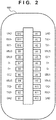
- the connector 101 has a pin assignment as that shown in Fig. 2.
- Fig. 2 is a view for illustrating the pin assignment of the connector 101.
- the connector 101 has a point-symmetric pin assignment as shown in Fig. 2 .
- One end of the pull-down resistor 102 is connected to the ground line via the switch 106.
- the voltage of the ground line is, for example, 0 V.
- the other end of the pull-down resistor 102 is connected to the CC terminal 101a and communication unit 103 via a node 107.
- the resistance of the pull-down resistor 102 is defined by the USB Type-C standard.
- the pull-down resistor 102 is used to change the voltage of the CC terminal 101a.
- the communication unit 103 is connected to the CC terminal 101a via the node 107.
- the communication unit 103 performs the predetermined USB PD communication with the power supply apparatus 120 via the CC terminal 101a and determines whether the communication unit 103 can perform the predetermined USB PD communication with the power supply apparatus 120.
- the control unit 105 is notified by the communication unit 103 as to whether the communication unit 103 is capable of performing the USB PD communication with the power supply apparatus 120.
- the determination unit 104 is connected to the VBUS terminal 101b.
- the determination unit 104 determines whether a first condition expressed as ⁇ V ⁇ A mV / ⁇ s is satisfied, and a second condition expressed as V ⁇ Vreq ⁇ B V is satisfied. If one of the first condition and the second condition is not satisfied, the determination unit 104 supplies, to the control unit 105, a signal indicating that the voltage applied from the power supply apparatus 120 to the VBUS terminal 101b is excessive. Note that arrangement examples of the determination unit 104 will be described later (see Figs. 5A and 5B ).
- ⁇ V of inequality (1) is a voltage variation per unit time of the VBUS terminal 101b.
- a of inequality (1) is the maximum allowable value (corresponding to the maximum value of the voltage variation ⁇ V allowed by the VBUS terminal 101b) of the voltage variation ⁇ V per unit time.
- a of inequality (1) is determined based on, for example, a voltage Vreq of inequality (2).
- the first embodiment and the other embodiments will describe a case in which the voltage Vreq is, for example, 9 V and A is, for example, 30 mV/ ⁇ s. Note that it is possible to determine A based on the USB PD standard.
- V of inequality (2) is the voltage of the VBUS terminal 101b.
- the voltage Vreq (corresponding to a predetermined voltage) of inequality (2) is the voltage that the electronic device 100 requests the power supply apparatus 120 to apply to the VBUS terminal 101b.
- B of inequality (2) is determined based on the voltage Vreq.
- Vreq ⁇ B indicates the maximum allowable voltage (corresponding to the maximum value of voltage allowed to be applied to the VBUS terminal 101b) of the VBUS terminal 101b.
- the first embodiment and the other embodiments will describe a case in which the voltage Vreq is, for example, 9 V and B is, for example, 1.05. Note that it is possible to determine B based on the USB PD standard.
- the control unit 105 includes a memory storing programs for controlling the components of the electronic device 100 and a processor (e.g., a hardware processor) that controls the components of the electronic device 100 by executing the corresponding programs stored in the memory.
- a processor e.g., a hardware processor
- the switch 106 is a switch for switching whether to connect the pull-down resistor 102 to the ground line.
- the switch 106 is set to an ON state (corresponding to a conductive state)
- the pull-down resistor 102 is connected to the ground line, and the voltage of the CC terminal 101a is pulled down until it is at the level of the pull-down voltage.
- the pull-down voltage suffices to be a voltage (for example, 2.45 V or lower) conforming to the USB Type-C standard.
- the switch 106 is set to an OFF state (corresponding to a nonconductive state)
- the pull-down resistor 102 is cut off from the ground line, and the voltage of the CC terminal 101a changes to a voltage (for example, 5 V) higher than the pull-down voltage.
- the switch 106 is arranged between the pull-down resistor 102 and the ground line, but the arrangement of the switch 106 is not limited to this.
- the switch 106 may be arranged between the node 107 and the pull-down resistor 102.
- the switch control unit 108 controls the switch 106 so that the switch 106 will be set to the ON state or the OFF state.
- the switch control unit 108 controls the switch 106 based on a control signal supplied from the control unit 105. If the determination unit 104 determines that one of the first condition expressed by inequality (1) and the second condition expressed by inequality (2) is not satisfied, the control unit 105 supplies the control signal to the switch control unit 108 to set the switch 106 in the OFF state.
- the switch control unit 108 sets the switch 106 in the OFF state based on the control signal supplied from the control unit 105.
- the voltage of the CC terminal 101a changes to a voltage (for example, 5 V) higher than the pull-down voltage.
- the power supply apparatus 120 determines that the power supply apparatus 120 has been disconnected from the electronic device 100. If it is determined that the power supply apparatus 120 has been disconnected from the electronic device 100, the power supply apparatus 120 stops applying the voltage to the VBUS terminal 101b. Note that it may be set so that the control unit 105 will supply, after a predetermined time has elapsed since the control signal for setting the switch 106 to the OFF state has been supplied to the switch control unit 108, the control signal for setting the switch 106 to the ON state. The predetermined time suffices to be a time enough for the power supply apparatus 120 to determine that the power supply apparatus 120 has been disconnected from the electronic device 100 based on the voltage change in the CC terminal 101a.
- the load unit 109 is connected to the VBUS terminal 101b.
- the load unit 109 includes components to provide a user with functions that serve as an image capture apparatus or a mobile device.
- the load unit 109 operates by power supplied from the power supply apparatus 120 or the battery.
- the power supplied from the power supply apparatus 120 is supplied to the load unit 109 via the VBUS terminal 101b.
- the power supply apparatus 120 operates as an external power source apparatus that supplies power to the electronic device 100 via the USB Type-C cable 130.
- the power supply apparatus 120 operates, for example, as an AC-USB adapter.
- the power supply apparatus 120 includes at least a plug 121 which is connected to an AC power source (not shown), a conversion unit (not shown) that converts AC voltage into DC voltage, and a connector (not shown) to which the USB Type-C cable 130 is connected.
- the power supply apparatus 120 is not limited to the AC-USB adapter.
- the power supply apparatus 120 may be a personal computer or a portable battery.
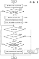
- Fig. 3 is a flowchart for illustrating an example of the operation of the electronic device 100 according to the first embodiment.
- step S301 the control unit 105 supplies, to the switch control unit 108, the control signal for setting the switch 106 to the ON state.
- the switch control unit 108 sets the switch 106 to the ON state based on the control signal supplied from the control unit 105.
- the pull-down resistor 102 is connected to the ground line, and the voltage of the CC terminal 101a is pulled down to the pull-down voltage.
- step S302 the control unit 105 determines whether the power supply apparatus 120 conforms to the USB PD standard based on whether the communication unit 103 can perform the predetermined USB PD communication with the power supply apparatus 120. If the communication unit 103 can perform the predetermined USB PD communication with the power supply apparatus 120 (YES in step S302), the control unit 105 determines that the power supply apparatus 120 conforms to the USB PD standard. If it is determined that the power supply apparatus 120 conforms to the USB PD standard, the control unit 105 proceeds to step S303. On the other hand, if the communication unit 103 cannot perform the predetermined USB PD communication with the power supply apparatus 120 (NO in step S302), the control unit 105 determines that the power supply apparatus 120 does not conform to the USB PD standard.
- the switch 106 is maintained in the ON state. In this case, power conforming not to the USB PD standard, but to the USB Type-C standard will be supplied from the power supply apparatus 120 to the electronic device 100.
- step S303 the communication unit 103 requests the power supply apparatus 120 via the CC terminal 101a to increase the voltage applied by the power supply apparatus 120 to the VBUS terminal 101b to the voltage Vreq.
- the first embodiment and the other embodiments will describe an example in which the voltage Vreq is, for example, 9 V.
- step S304 the control unit 105 requests the determination unit 104 to execute a determination operation.
- the determination unit 104 starts the determination operation.
- the monitoring of the voltage of the VBUS terminal 101b is started by the determination unit 104.
- step S305 the determination unit 104 detects the voltage of the VBUS terminal 101b and determines whether it satisfies the first condition expressed by inequality (1). For example, the determination unit 104 determines, based on the difference between the voltage of the VBUS terminal 101b previously detected by the determination unit 104 and the voltage of the VBUS terminal 101b most recently detected by the determination unit 104, whether the voltage variation ⁇ V per unit time of the VBUS terminal 101b is less than 30 mV/ ⁇ s (less than a first predetermined value). If the voltage variation ⁇ V per unit time of the VBUS terminal 101b is less than 30 mV/ ⁇ s (YES in step S305), the determination unit 104 determines that the first condition is satisfied.
- step S306 the control unit 105 proceeds to step S306.
- the determination unit 104 determines that the first condition is not satisfied.
- the determination unit 104 supplies, to the control unit 105, a signal indicating that the voltage applied from the power supply apparatus 120 to the VBUS terminal 101b is excessive, and the control unit 105 proceeds to step S309.
- step S309 the control unit 105 determines that the voltage applied from the power supply apparatus 120 to the VBUS terminal 101b is excessive.
- the control unit 105 controls the determination unit 104 to stop the determination operation, and supplies, to the switch control unit 108, the control signal for setting the switch 106 to the OFF state.
- the switch control unit 108 sets the switch 106 to the OFF state based on the control signal supplied from the control unit 105.
- the pull-down resistor 102 is cut off from the ground line when the switch 106 is set to the OFF state, and the voltage of the CC terminal 101a changes to a voltage (for example, 5 V) higher than the pull-down voltage.
- the power supply apparatus 120 determines that the power supply apparatus 120 has been disconnected from the electronic device 100. If it is determined that the power supply apparatus 120 has been disconnected from the electronic device 100, the power supply apparatus 120 stops applying the voltage to the VBUS terminal 101b. As a result, the electronic device 100 can protect the internal circuitry (the load unit 109 or the like) connected to the VBUS terminal 101b of the electronic device 100 from an excessive voltage.
- step S306 the determination unit 104 detects the voltage of the VBUS terminal 101b and determines whether it satisfies the second condition expressed by inequality (2). For example, the determination unit 104 determines whether the voltage of the VBUS terminal 101b is lower than 9.45 V (corresponding to a second predetermined value). If the voltage of the VBUS terminal 101b is lower than 9.45 V (YES in step S306), the determination unit 104 determines that the second condition is satisfied. If it is determined that the second condition is satisfied, the control unit 105 proceeds to step S307. On the other hand, if the maximum allowable voltage of the VBUS terminal 101b is equal to or higher than 9.45 V (NO in step S306), the determination unit 104 determines that the second condition is not satisfied.
- the determination unit 104 supplies, to the control unit 105, a signal indicating that the voltage applied from the power supply apparatus 120 to the VBUS terminal 101b is excessive, and the control unit 105 proceeds to step S309. Note that the determination unit 104 will also determine that the second condition is not satisfied in a case in which the repetition of the processes of steps S305, S306, and S307 has exceeded a predetermined count.
- step S307 the communication unit 103 determines whether it has been able to receive a voltage change completion signal from the power supply apparatus 120 via the CC terminal 101a.
- the voltage change completion signal contains information indication the completion of the operation to increase the voltage applied to the VBUS terminal 101b to the voltage Vreq.
- the control unit 105 is notified by the communication unit 103 as to whether the communication unit 103 has been able to receive the voltage change completion signal from the power supply apparatus 120 via the CC terminal 101a.
- step S307 If the communication unit 103 has been able to receive the voltage change completion signal from the power supply apparatus 120 via the CC terminal 101a (YES in step S307), the control unit 105 determines that the operation to increase the voltage applied to the VBUS terminal 101b to the voltage Vreq has been completed, and proceeds to step S308. If the communication unit 103 has not been able to receive the voltage change completion signal from the power supply apparatus 120 via the CC terminal 101a (NO in step S307), the control unit 105 returns to step S305.
- step S308 the control unit 105 requests the determination unit 104 to stop the determination operation.
- the determination unit 104 accordingly stops the determination operation.
- the switch 106 is maintained in the ON state. By maintaining the switch 106 in the ON state, the power supply from the power supply apparatus 120 to the electronic device 100 is maintained even after step S308.
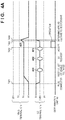
- Figs. 4A and 4B are timing charts for illustrating examples of the changes in the states of the CC terminal 101a, the VBUS terminal 101b, and the determination unit 104.
- T401 indicates the point at which the plug 131 of the USB Type-C cable 130 has been inserted to the connector 101 of the electronic device 100 in a state in which the power supply apparatus 120 and the USB Type-C cable 130 are connected.
- the voltage of the CC terminal 101a is a voltage (for example, 5 V) higher than the pull-down voltage. Since the power supply apparatus 120 will determine that the power supply apparatus 120 is not connected to the electronic device 100 when the voltage of the CC terminal 101a is a voltage (for example, 5 V) higher than the pull-down voltage, the power supply apparatus 120 will not apply the voltage to the VBUS terminal 101b.
- the voltage of the VBUS terminal 101b is, for example, 0 V.
- step S301 the control unit 105 supplies, to the switch control unit 108, the control signal to set the switch 106 to the ON state.
- the switch control unit 108 sets the switch 106 to the ON state based on the control signal supplied from the control unit 105.
- the pull-down resistor 102 is connected to the ground line, and the voltage of the CC terminal 101a is pulled down to the pull-down voltage (for example, 2.45 V).
- the power supply apparatus 120 determines that the power supply apparatus 120 has been connected to the electronic device 100, and applies, to the VBUS terminal 101b, a voltage (for example, 5 V) higher than the pull-down voltage.
- USB PD communications 401, 402, and 403 are communications conforming to the USB PD standard.
- the power supply apparatus 120 transmits a list of usable voltages to the electronic device 100.
- the communication unit 103 receives the list of usable voltages from the power supply apparatus 120 via the CC terminal 101a and notifies the control unit 105 of the received list. If the control unit 105 is notified of the list of usable voltages from the communication unit 103 before the elapse of a predetermined time from the start of the USB PD communication 401, the control unit 105 will determine that the communication unit 103 has been able to perform the USB PD communication with the power supply apparatus 120. In this case, the control unit 105 will determine that the power supply apparatus 120 conforms to the USB PD standard (YES in step S302).
- the control unit 105 determines that the communication unit 103 has not been able to perform the USB PD communication with the power supply apparatus 120. In this case, the control unit 105 will determine that the power supply apparatus 120 does not conform to the USB PD standard (NO in step S302).
- the communication unit 103 After it is determined that the power supply apparatus 120 conforms to the USB PD standard, the communication unit 103 performs the USB PD communication 402 with the power supply apparatus 120. In the USB PD communication 402, the communication unit 103 requests the power supply apparatus 120 via the CC terminal 101a to increase the voltage applied by the power supply apparatus 120 to the VBUS terminal 101b to the voltage Vreq (for example, 9 V) (step S303).
- Vreq for example, 9 V
- the communication unit 103 After requesting the power supply apparatus 120 via the CC terminal 101a to increase the voltage applied by the power supply apparatus 120 to the VBUS terminal 101b to the voltage Vreq (for example, 9 V), the communication unit 103 performs the USB PD communication 403 with the power supply apparatus 120.
- the power supply apparatus 120 transmits, to the electronic device 100, an acceptance signal that includes information indicating that it has accepted the request to increase the voltage applied to the VBUS terminal 101b to the voltage Vreq.
- the communication unit 103 determines whether it has been able to receive the acceptance signal from the power supply apparatus 120 via the CC terminal 101a.
- the control unit 105 is notified by the communication unit 103 as to whether the communication unit 103 has been able to receive the acceptance signal from the power supply apparatus 120 via the CC terminal 101a.
- the control unit 105 After the communication unit 103 has received the acceptance signal from the power supply apparatus 120 via the CC terminal 101a, the control unit 105 requests the determination unit 104 to start the determination operation described above (step S304). T402 indicates the point at which the determination operation is started by the determination unit 104.
- the determination unit 104 repetitively determines whether both the first condition expressed by inequality (1) and the second condition expressed by inequality (2) are satisfied.
- T403 indicates the point at which the voltage variation ⁇ V per unit time of the VBUS terminal 101b is, for example, equal to or more than 30 mV/ ⁇ s.
- the determination unit 104 determines that the first condition expressed by inequality (1) is not satisfied (NO in step S305).
- the determination unit 104 supplies, to the control unit 105, a signal indicating that the voltage applied from the power supply apparatus 120 to the VBUS terminal 101b is excessive.
- the control unit 105 controls the determination unit 104 to stop the determination operation and supplies a control signal, to the switch control unit 108, to set the switch 106 to the OFF state.
- step S309 the switch control unit 108 sets the switch 106 to the OFF state based on the control signal supplied from the control unit 105. After the switch 106 is set to the OFF state, the pull-down resistor 102 is cut off from the ground line, and the voltage of the CC terminal 101a increases to a voltage (for example, 5 V) higher than the pull-down voltage.
- T404 indicates the point at which the voltage of the CC terminal 101a has increased to a voltage (for example, 5 V) higher than the pull-down voltage.
- the power supply apparatus 120 detects that the voltage of the CC terminal 101a has become a voltage (for example, 5 V) higher than the pull-down voltage and determines that the power supply apparatus 120 has been disconnected from the electronic device 100.
- the power supply apparatus 120 stops applying the voltage to the VBUS terminal 101b.
- the voltage of the VBUS terminal 101b changes to 0 V.
- the electronic device 100 can protect the internal circuitry (the load unit 109 or the like) connected to the VBUS terminal 101b of the electronic device 100 from an excessive voltage.
- the determination unit 104 repetitively determines whether both the first condition expressed by inequality (1) and the second condition expressed by inequality (2) are satisfied.
- the determination unit 104 determines that the second condition expressed by inequality (2) is not satisfied (NO in step S306). When it is determined that the second condition is not satisfied, the determination unit 104 supplies, to the control unit 105, a signal indicating that the voltage applied from the power supply apparatus 120 to the VBUS terminal 101b is excessive. Then, in step S309, the control unit 105 controls the determination unit 104 to stop the determination operation and supplies a control signal, to the switch control unit 108, to set the switch 106 to the OFF state.
- step S309 the switch control unit 108 sets the switch 106 to the OFF state based on the control signal supplied from the control unit 105. After the switch 106 is set to the OFF state, the pull-down resistor 102 is cut off from the ground line, and the voltage of the CC terminal 101a increases to a voltage (for example, 5 V) higher than the pull-down voltage.
- T404 indicates the point at which the voltage of the CC terminal 101a has changed to a voltage (for example, 5 V) higher than the pull-down voltage.
- the power supply apparatus 120 detects that the voltage of the CC terminal 101a has changed to a voltage (for example, 5 V) higher than the pull-down voltage, and determines that the power supply apparatus 120 has been disconnected from the electronic device 100.
- the power supply apparatus 120 stops applying the voltage to the VBUS terminal 101b.
- the voltage of the VBUS terminal 101b changes to 0 V.
- the electronic device 100 can protect the internal circuitry (the load unit 109 or the like) connected to the VBUS terminal 101b of the electronic device 100 from an excessive voltage.
- Fig. 5A is a block diagram for illustrating an example of components of the determination unit 104.
- the determination unit 104 includes an AD conversion unit 501 and a processing unit 502.
- the operation of the processing unit 502 is controlled by the control unit 105, and the operation of the AD conversion unit 501 is controlled by the processing unit 502.
- the AD conversion unit 501 is connected to the VBUS terminal 101b.
- the AD conversion unit 501 converts the voltage of the VBUS terminal 101b into a digital signal.
- the generated digital signal is supplied from the AD conversion unit 501 to the processing unit 502.
- a known AD conversion unit may be used as the AD conversion unit 501.
- the AD conversion unit 501 may be, for example, a successive approximation AD conversion unit or a sigma-delta AD conversion unit. Note that the voltage of the VBUS terminal 101b may be divided by a voltage dividing resistor before it is applied to the AD conversion unit 501.
- the processing unit 502 determines, based on the digital signal supplied from the AD conversion unit 501, whether both the first condition expressed by inequality (1) and the second condition expressed by inequality (2) are satisfied.
- the processing unit 502 supplies a timing signal to the AD conversion unit 501 at an arbitrary timing (e.g., periodic timing).
- the AD conversion unit 501 generates a digital signal indicating the voltage of the VBUS terminal 101b in accordance with the timing signal supplied from the processing unit 502, and supplies the generated signal to the processing unit 502.
- a digital signal is periodically supplied from the AD conversion unit 501 to the processing unit 502.
- the processing unit 502 includes a memory 509.
- the memory 509 stores a digital signal indicating the voltage of the VBUS terminal 101b most recently supplied from the AD conversion unit 501 and a digital signal indicating the voltage of the VBUS terminal 101b previously supplied from the AD conversion unit 501.
- the processing unit 502 calculates the voltage variation ⁇ V per unit time of the VBUS terminal 101b based on the difference between two digital signals stored in the memory 509.
- V x is the previous voltage of the VBUS terminal 101b stored in the memory 509
- V x+1 is the most recent voltage of the VBUS terminal 101b stored in the memory 509
- t corresponds to a time interval from the point at which the previous voltage of the VBUS terminal 101b has been detected to the point at which the most recent voltage of the VBUS terminal 101b has been detected (alternatively, the time interval at which a digital signal is supplied from the AD conversion unit 501 to the processing unit 502).
- the processing unit 502 determines, based on the calculated voltage variation ⁇ V, whether the first condition expressed by inequality (1) is satisfied. For example, the processing unit 502 compares the calculated voltage variation ⁇ V with 30 mV/ ⁇ s. If the calculated voltage variation ⁇ V is lower than 30 mV/ ⁇ s (YES in step S305), the determination unit 104 determines that the first condition is satisfied. If the first condition is satisfied, the control unit 105 proceeds to step S306. If the calculated voltage variation ⁇ V equal to or higher than 30 mV/ ⁇ s (NO in step S305), the determination unit 104 determines that the first condition is not satisfied. If the first condition is not satisfied, the determination unit 104 supplies, to the control unit 105, a signal indicating that the voltage applied from the power supply apparatus 120 to the VBUS terminal 101b is excessive, and the control unit 105 proceeds to step S309.
- step S306 If the most recent voltage detected by the AD conversion unit 501 is equal to higher than 9.45 V (NO in step S306), the determination unit 104 will determine that the second condition is not satisfied. When the second condition is not satisfied, the determination unit 104 supplies, to the control unit 105, the signal indicating that the voltage applied from the power supply apparatus 120 to the VBUS terminal 101b is excessive, and the control unit 105 proceeds to step S309.
- the control unit 105 supplies, to the switch control unit 108, the control signal for setting the switch 106 to the OFF state.
- the switch control unit 108 sets the switch 106 to the OFF state based on the control signal supplied from the control unit 105 (step S309).
- Fig. 5B is a block diagram for illustrating another example of components of the determination unit 104.
- the determination unit 104 includes a comparator 503, a ramp wave generating circuit 504, and a reference voltage generating circuit 505.
- the operations of the comparator 503, the ramp wave generating circuit 504, and the reference voltage generating circuit 505 are controlled by the control unit 105.
- the comparator 503 is a three-input comparator that includes a first input terminal Vin+, a second input terminal Vin-1, and a third input terminal Vin-2.
- the first input terminal Vin+ of the comparator 503 is connected to the VBUS terminal 101b, and the voltage of the VBUS terminal 101b is applied to the first input terminal Vin+.
- the second input terminal Vin-1 of the comparator 503 is connected to the ramp wave generating circuit 504, and the ramp wave generated by the ramp wave generating circuit 504 is input to the second input terminal Vin-1.
- the third input terminal Vin-2 of the comparator 503 is connected to the reference voltage generating circuit 505, and a reference voltage generated by the reference voltage generating circuit 505 is applied to the third input terminal Vin-2.
- the comparator 503 In a case in which the voltage of the VBUS terminal 101b is lower than the voltage of the ramp wave supplied from the ramp wave generating circuit 504 and is lower than the reference voltage supplied from the reference voltage generating circuit 505, the comparator 503 outputs a signal OUT at low level. In a case in which the voltage of the VBUS terminal 101b is equal to or higher than the voltage of the ramp wave supplied from the ramp wave generating circuit 504 or is equal to or higher than the reference voltage supplied from the reference voltage generating circuit 505, the comparator 503 outputs the signal OUT at high level. The signal OUT output from the comparator 503 is input to the control unit 105.
- the signal OUT output from the comparator 503 at high level means that one of the first condition expressed by inequality (1) and the second condition expressed by inequality (2) is not satisfied.
- the control unit 105 supplies, to the switch control unit 108, the control signal to set the switch 106 to the OFF state.
- a first control signal CTL1 supplied from the control unit 105 to the comparator 503 is at high level, the comparator 503 performs a comparison operation.
- the comparator 503 does not perform the comparison operation.
- the ramp wave generating circuit 504 generates a ramp wave (corresponding to the reference signal) which is a ramp-shaped analog signal.
- the ramp wave output from the ramp wave generating circuit 504 is input to the second input terminal Vin-1 of the comparator 503.
- the ramp wave generating circuit 504 outputs a ramp wave corresponding to 30 mV/ ⁇ s.
- the ramp wave generating circuit 504 starts the ramp wave output.
- the ramp wave generating circuit 504 stops the ramp wave output.
- the reference voltage generating circuit 505 includes a first resistor 506 which is a fixed resistor and a second resistor 507 which is a variable resistor, and the reference voltage generating circuit generates a reference voltage corresponding to Vreq ⁇ B.
- One end of the first resistor 506 is connected to, for example, the power source (the battery or the like) of the electronic device 100.
- the other end of the first resistor 506 is connected to one end of the second resistor 507 and the third input terminal Vin-2 of the comparator 503 via a node 508.
- the other end of the second resistor 507 is connected to the ground line.
- the reference voltage generating circuit 505 generates the reference voltage by dividing the voltage supplied from the power source of the electronic device 100 by the first resistor 506 and the second resistor 507.
- the reference voltage generated by the reference voltage generating circuit 505 is applied to the third input terminal Vin-2 of the comparator 503.
- the reference voltage generated by the reference voltage generating circuit 505 is changed when the control unit 105 controls the resistance value of the second resistor 507.
- the control unit 105 can control the resistance value of the second resistor 507 to change the value of the reference voltage to a value depending on the voltage Vreq.
- the voltage of the VBUS terminal 101b may be divided by a voltage dividing resistor before it is applied to the first input terminal Vin+ of the comparator 503. For example, it may be set so that a voltage which is a times (a ⁇ 1) the voltage of the VBUS terminal 101b will be applied to the first input terminal Vin+ of the comparator 503.
- the ramp wave generating circuit 504 will output a ramp wave corresponding to a ⁇ 30 mV/ ⁇ s.
- the reference voltage generating circuit 505 will generate a reference voltage of a ⁇ Vreq ⁇ 1.05 V.
- the comparator 503 compares the voltage (corresponding to the voltage of the VBUS terminal 101b) of the first input terminal Vin+ and the voltage (corresponding to, for example, 30 mV/ ⁇ s) of the second input terminal Vin-1. If the voltage of the first input terminal Vin+ is lower than the voltage of the second input terminal Vin-1 (YES in step S305), the determination unit 104 will determine that the first condition expressed by inequality (1) is satisfied. If the first condition is satisfied, the control unit 105 proceeds to step S306. If the voltage of the first input terminal Vin+ is equal to or higher than the voltage of the second input terminal Vin-1 (NO in step S305), the determination unit 104 will determine that the first condition expressed by inequality (1) is not satisfied. If the first condition is not satisfied, the determination unit 104 supplies, to the control unit 105, a signal indicating that the voltage applied from the power supply apparatus 120 to the VBUS terminal 101b is excessive, and the control unit 105 proceeds to step S309.
- the comparator 503 compares the voltage (corresponding to the voltage of the VBUS terminal 101b) of the first input terminal Vin+ and the voltage (corresponding to, for example, 9.45 V) of the third input terminal Vin-2. If the voltage of the first input terminal Vin+ is lower than the voltage of the third input terminal Vin-2 (YES in step S306), the determination unit 104 will determine that the second condition expressed by inequality (2) is satisfied. If the second condition is satisfied, the control unit 105 proceeds to step S307. If the voltage of the first input terminal Vin+ is equal to or higher than the voltage of the third input terminal Vin-2 (NO in step S306), the determination unit 104 will determine that the second condition is not satisfied. If the second condition is not satisfied, the determination unit 104 supplies, to the control unit 105, a signal indicating that the voltage applied from the power supply apparatus 120 to the VBUS terminal 101b is excessive, and the control unit 105 proceeds to step S309.
- a signal indicating that the voltage of the VBUS terminal 101b is excessive is supplied from the comparator 503 to the control unit 105.
- the control unit 105 supplies, to the switch control unit 108, the control signal for setting the switch 106 to the OFF state.
- the switch control unit 108 sets the switch 106 to the OFF state based on the control signal supplied from the control unit 105.
- the control unit 105 will determine that the voltage applied from the power supply apparatus 120 to the VBUS terminal 101b is excessive, and will set the switch 106 to the OFF state. Since the voltage of the CC terminal 101a will change to a voltage (for example, 5 V) higher than the pull-down voltage when the switch 106 is set in the OFF state, the power supply apparatus 120 will determine that the power supply apparatus 120 has been disconnected from the electronic device 100. As a result, the power supply apparatus 120 stops the voltage application to the VBUS terminal 101b. Therefore, according to the first embodiment, the electronic device 100 can protect the internal circuitry (the load unit 109 or the like) connected to the VBUS terminal 101b of the electronic device 100 from an excessive voltage.
- the internal circuitry the load unit 109 or the like
- Various kinds of functions, processes, or methods described in the first embodiment can be implemented by a personal computer, a microcomputer, a CPU (Central Processing Unit), a processor, or the like by using corresponding programs.
- a personal computer, a microcomputer, a CPU (Central Processing Unit), a processor, or the like will be referred to as a "computer X" hereinafter.
- a program for controlling the computer X that is, a program for implementing one of the various kinds of functions, processes, or methods described in the first embodiment will be referred to as a "program Y".
- the computer-readable storage medium according to the second embodiment includes at least one of a hard disk device, a magnetic storage device, an optical storage device, a magneto-optical storage device, a memory card, a volatile memory, a nonvolatile memory, or the like.
- the computer-readable storage medium according to the second embodiment is a non-transitory storage medium.
- An electronic device (100) includes a monitoring means (104) for monitoring a voltage of a first terminal that receives power supplied from a power supply apparatus (120), and a control means (105) for performing control so as to stop the power supply from the power supply apparatus (120) if a voltage variation per unit time of the first terminal is not less than a first predetermined value or the voltage of the first terminal is not less than a second predetermined value.
Landscapes
- Engineering & Computer Science (AREA)
- Theoretical Computer Science (AREA)
- Physics & Mathematics (AREA)
- General Engineering & Computer Science (AREA)
- General Physics & Mathematics (AREA)
- Electromagnetism (AREA)
- Computer Hardware Design (AREA)
- Power Sources (AREA)
- Emergency Protection Circuit Devices (AREA)
- Direct Current Feeding And Distribution (AREA)
Abstract
Description
- Aspects of the disclosure generally relate to an electronic device and a control method thereof.
- A power supply apparatus (such as a personal computer, an AC-USB adapter, or the like) that includes a USB (Universal Serial Bus) interface can supply power, via a USB cable, to an electronic device that includes a USB interface. Japanese Patent Laid-Open No.
9-215176 - A power supply apparatus conforming to USB Power Delivery (USB PD) standard can supply power of a maximum of 100 W (5 A, 20 V) to an electronic device through a USB interface. Hence, depending on the state or the arrangement of the power supply apparatus, an excessive voltage exceeding the maximum value of voltage that can be applied from the power supply apparatus to the electronic device may be applied to a VBUS terminal of the electronic device. If such an excessive voltage is applied to the VBUS terminal of the electronic device, it may cause internal circuitry connected to the VBUS terminal of the electronic device to break down.
- According to an aspect of the embodiments, an electronic device or a control method more improved than the electronic device or control method described above is provided.
- According to an aspect of the embodiments, internal circuitry of the electronic device can be protected from an excessive voltage.
- The present invention in its first aspect provides an electronic device as specified in
claims 1 to 10. - The present invention in its second aspect provides a method as specified in claim 11.
- The present invention in its third aspect provides a computer program as specified in
claim 12. - Further aspects of the embodiments will become apparent from the following embodiments.
-
-
Fig. 1 is a block diagram for illustrating an example of components of anelectronic device 100 according to the first embodiment; -
Fig. 2 is a view for illustrating a pin assignment of aconnector 101; -
Fig. 3 is a flowchart for illustrating an example of an operation of theelectronic device 100 according to the first embodiment; -
Fig. 4A is a timing chart for illustrating an example of changes in the states of aCC terminal 101a, aVBUS terminal 101b, and adetermination unit 104; -
Fig. 4B is a timing chart for illustrating an example of changes in the states of theCC terminal 101a, the VBUSterminal 101b, and thedetermination unit 104; -
Fig. 5A is a block diagram for illustrating an example of components of thedetermination unit 104; and -
Fig. 5B is a block diagram for illustrating another example of components of thedetermination unit 104. - Exemplary embodiments, features, and aspects of the disclosure will be described below with reference to the drawings. However, aspects of the disclosure are not limited to the following embodiments.
- An example of components of an
electronic device 100 according to the first embodiment will be described first with reference toFig. 1. Fig. 1 is a block diagram for illustrating components of theelectronic device 100 according to the first embodiment. Theelectronic device 100 is an electronic device capable of acting as an image capture apparatus or a mobile device. - As shown in
Fig. 1 , theelectronic device 100 includes aconnector 101, a pull-down resistor 102, acommunication unit 103, adetermination unit 104, acontrol unit 105, aswitch 106, aswitch control unit 108, aload unit 109, and a battery (not shown). The battery can be removed from theelectronic device 100 by the user. - The
connector 101 is a USB Type-C connector (receptacle) to which aplug 131 of a USB Type-C cable 130 is connected. In this specification, a connector conforming to USB (Universal Serial Bus) Type-C standard will be referred to as a USB Type-C connector, and a cable conforming to the USB Type-C standard will be referred to as a USB Type-C cable. Apower supply apparatus 120 is connected to theconnector 101 via the USB Type-C cable 130. Theconnector 101 receives power supplied from thepower supply apparatus 120 via the USB Type-Ccable 130. - The
connector 101 includes at least a CC (Configuration Channel)terminal 101a, aVBUS terminal 101b, and aGND terminal 101c. TheCC terminal 101a is used to perform predetermined communication (to be referred to as predetermined USB PD communication) conforming to USB PD (Power Delivery) standard with thepower supply apparatus 120. TheCC terminal 101a is used for determining the power supply capability of thepower supply apparatus 120 by a method conforming to the USB Type-C standard. The VBUSterminal 101b is used to supply power from thepower supply apparatus 120 to theelectronic device 100. TheGND terminal 101c is connected to a ground line. Theconnector 101 has a pin assignment as that shown inFig. 2. Fig. 2 is a view for illustrating the pin assignment of theconnector 101. Theconnector 101 has a point-symmetric pin assignment as shown inFig. 2 . - One end of the pull-
down resistor 102 is connected to the ground line via theswitch 106. The voltage of the ground line is, for example, 0 V. The other end of the pull-down resistor 102 is connected to theCC terminal 101a andcommunication unit 103 via anode 107. The resistance of the pull-down resistor 102 is defined by the USB Type-C standard. The pull-down resistor 102 is used to change the voltage of theCC terminal 101a. - The
communication unit 103 is connected to theCC terminal 101a via thenode 107. Thecommunication unit 103 performs the predetermined USB PD communication with thepower supply apparatus 120 via theCC terminal 101a and determines whether thecommunication unit 103 can perform the predetermined USB PD communication with thepower supply apparatus 120. Thecontrol unit 105 is notified by thecommunication unit 103 as to whether thecommunication unit 103 is capable of performing the USB PD communication with thepower supply apparatus 120. - The
determination unit 104 is connected to the VBUSterminal 101b. Thedetermination unit 104 determines whether a first condition expressed as

determination unit 104 supplies, to thecontrol unit 105, a signal indicating that the voltage applied from thepower supply apparatus 120 to theVBUS terminal 101b is excessive. Note that arrangement examples of thedetermination unit 104 will be described later (seeFigs. 5A and5B ). - ΔV of inequality (1) is a voltage variation per unit time of the
VBUS terminal 101b. A of inequality (1) is the maximum allowable value (corresponding to the maximum value of the voltage variation ΔV allowed by theVBUS terminal 101b) of the voltage variation ΔV per unit time. A of inequality (1) is determined based on, for example, a voltage Vreq of inequality (2). The first embodiment and the other embodiments will describe a case in which the voltage Vreq is, for example, 9 V and A is, for example, 30 mV/µs. Note that it is possible to determine A based on the USB PD standard. - V of inequality (2) is the voltage of the
VBUS terminal 101b. The voltage Vreq (corresponding to a predetermined voltage) of inequality (2) is the voltage that theelectronic device 100 requests thepower supply apparatus 120 to apply to theVBUS terminal 101b. B of inequality (2) is determined based on the voltage Vreq. Vreq × B indicates the maximum allowable voltage (corresponding to the maximum value of voltage allowed to be applied to the VBUS terminal 101b) of theVBUS terminal 101b. The first embodiment and the other embodiments will describe a case in which the voltage Vreq is, for example, 9 V and B is, for example, 1.05. Note that it is possible to determine B based on the USB PD standard. - The
control unit 105 includes a memory storing programs for controlling the components of theelectronic device 100 and a processor (e.g., a hardware processor) that controls the components of theelectronic device 100 by executing the corresponding programs stored in the memory. - The
switch 106 is a switch for switching whether to connect the pull-down resistor 102 to the ground line. When theswitch 106 is set to an ON state (corresponding to a conductive state), the pull-down resistor 102 is connected to the ground line, and the voltage of theCC terminal 101a is pulled down until it is at the level of the pull-down voltage. Note that the pull-down voltage suffices to be a voltage (for example, 2.45 V or lower) conforming to the USB Type-C standard. When theswitch 106 is set to an OFF state (corresponding to a nonconductive state), the pull-down resistor 102 is cut off from the ground line, and the voltage of theCC terminal 101a changes to a voltage (for example, 5 V) higher than the pull-down voltage. Note that the first embodiment and the other embodiments will describe an example in which theswitch 106 is arranged between the pull-down resistor 102 and the ground line, but the arrangement of theswitch 106 is not limited to this. For example, theswitch 106 may be arranged between thenode 107 and the pull-down resistor 102. - The
switch control unit 108 controls theswitch 106 so that theswitch 106 will be set to the ON state or the OFF state. Theswitch control unit 108 controls theswitch 106 based on a control signal supplied from thecontrol unit 105. If thedetermination unit 104 determines that one of the first condition expressed by inequality (1) and the second condition expressed by inequality (2) is not satisfied, thecontrol unit 105 supplies the control signal to theswitch control unit 108 to set theswitch 106 in the OFF state. Theswitch control unit 108 sets theswitch 106 in the OFF state based on the control signal supplied from thecontrol unit 105. When theswitch 106 is set to the OFF state, the voltage of theCC terminal 101a changes to a voltage (for example, 5 V) higher than the pull-down voltage. When the voltage of theCC terminal 101a changes to a voltage (for example, 5 V) higher than the pull-down voltage, thepower supply apparatus 120 determines that thepower supply apparatus 120 has been disconnected from theelectronic device 100. If it is determined that thepower supply apparatus 120 has been disconnected from theelectronic device 100, thepower supply apparatus 120 stops applying the voltage to theVBUS terminal 101b. Note that it may be set so that thecontrol unit 105 will supply, after a predetermined time has elapsed since the control signal for setting theswitch 106 to the OFF state has been supplied to theswitch control unit 108, the control signal for setting theswitch 106 to the ON state. The predetermined time suffices to be a time enough for thepower supply apparatus 120 to determine that thepower supply apparatus 120 has been disconnected from theelectronic device 100 based on the voltage change in theCC terminal 101a. - The
load unit 109 is connected to theVBUS terminal 101b. Theload unit 109 includes components to provide a user with functions that serve as an image capture apparatus or a mobile device. Theload unit 109 operates by power supplied from thepower supply apparatus 120 or the battery. The power supplied from thepower supply apparatus 120 is supplied to theload unit 109 via theVBUS terminal 101b. - The
power supply apparatus 120 operates as an external power source apparatus that supplies power to theelectronic device 100 via the USB Type-C cable 130. Thepower supply apparatus 120 operates, for example, as an AC-USB adapter. Thepower supply apparatus 120 includes at least aplug 121 which is connected to an AC power source (not shown), a conversion unit (not shown) that converts AC voltage into DC voltage, and a connector (not shown) to which the USB Type-C cable 130 is connected. Note that thepower supply apparatus 120 is not limited to the AC-USB adapter. For example, thepower supply apparatus 120 may be a personal computer or a portable battery. -
Fig. 3 is a flowchart for illustrating an example of the operation of theelectronic device 100 according to the first embodiment. - When the
plug 131 of the USB Type-C cable 130 is inserted to theconnector 101 of theelectronic device 100, the process of step S301 is started. In step S301, thecontrol unit 105 supplies, to theswitch control unit 108, the control signal for setting theswitch 106 to the ON state. Theswitch control unit 108 sets theswitch 106 to the ON state based on the control signal supplied from thecontrol unit 105. As a result, the pull-down resistor 102 is connected to the ground line, and the voltage of theCC terminal 101a is pulled down to the pull-down voltage. - In step S302, the
control unit 105 determines whether thepower supply apparatus 120 conforms to the USB PD standard based on whether thecommunication unit 103 can perform the predetermined USB PD communication with thepower supply apparatus 120. If thecommunication unit 103 can perform the predetermined USB PD communication with the power supply apparatus 120 (YES in step S302), thecontrol unit 105 determines that thepower supply apparatus 120 conforms to the USB PD standard. If it is determined that thepower supply apparatus 120 conforms to the USB PD standard, thecontrol unit 105 proceeds to step S303. On the other hand, if thecommunication unit 103 cannot perform the predetermined USB PD communication with the power supply apparatus 120 (NO in step S302), thecontrol unit 105 determines that thepower supply apparatus 120 does not conform to the USB PD standard. If it is determined that thepower supply apparatus 120 does not conform to the USB PD standard, theswitch 106 is maintained in the ON state. In this case, power conforming not to the USB PD standard, but to the USB Type-C standard will be supplied from thepower supply apparatus 120 to theelectronic device 100. - In step S303, the
communication unit 103 requests thepower supply apparatus 120 via theCC terminal 101a to increase the voltage applied by thepower supply apparatus 120 to the VBUS terminal 101b to the voltage Vreq. The first embodiment and the other embodiments will describe an example in which the voltage Vreq is, for example, 9 V. - In step S304, the
control unit 105 requests thedetermination unit 104 to execute a determination operation. Thedetermination unit 104 starts the determination operation. As a result, the monitoring of the voltage of theVBUS terminal 101b is started by thedetermination unit 104. - In step S305, the
determination unit 104 detects the voltage of the VBUS terminal 101b and determines whether it satisfies the first condition expressed by inequality (1). For example, thedetermination unit 104 determines, based on the difference between the voltage of the VBUS terminal 101b previously detected by thedetermination unit 104 and the voltage of the VBUS terminal 101b most recently detected by thedetermination unit 104, whether the voltage variation ΔV per unit time of theVBUS terminal 101b is less than 30 mV/µs (less than a first predetermined value). If the voltage variation ΔV per unit time of theVBUS terminal 101b is less than 30 mV/µs (YES in step S305), thedetermination unit 104 determines that the first condition is satisfied. In a case in which it is determined that the first condition is satisfied, thecontrol unit 105 proceeds to step S306. On the other hand, if the voltage variation ΔV per unit time of theVBUS terminal 101b is equal to or more than 30 mV/µs (equal to or more than the first predetermined value) (NO in step S305), thedetermination unit 104 determines that the first condition is not satisfied. In a case in which it is determined that the first condition is not satisfied, thedetermination unit 104 supplies, to thecontrol unit 105, a signal indicating that the voltage applied from thepower supply apparatus 120 to theVBUS terminal 101b is excessive, and thecontrol unit 105 proceeds to step S309. - In step S309, the
control unit 105 determines that the voltage applied from thepower supply apparatus 120 to theVBUS terminal 101b is excessive. In addition, thecontrol unit 105 controls thedetermination unit 104 to stop the determination operation, and supplies, to theswitch control unit 108, the control signal for setting theswitch 106 to the OFF state. Theswitch control unit 108 sets theswitch 106 to the OFF state based on the control signal supplied from thecontrol unit 105. The pull-down resistor 102 is cut off from the ground line when theswitch 106 is set to the OFF state, and the voltage of theCC terminal 101a changes to a voltage (for example, 5 V) higher than the pull-down voltage. If the voltage of theCC terminal 101a changes to a voltage (for example, 5 V) higher than the pull-down voltage, thepower supply apparatus 120 determines that thepower supply apparatus 120 has been disconnected from theelectronic device 100. If it is determined that thepower supply apparatus 120 has been disconnected from theelectronic device 100, thepower supply apparatus 120 stops applying the voltage to theVBUS terminal 101b. As a result, theelectronic device 100 can protect the internal circuitry (theload unit 109 or the like) connected to the VBUS terminal 101b of theelectronic device 100 from an excessive voltage. - In step S306, the
determination unit 104 detects the voltage of the VBUS terminal 101b and determines whether it satisfies the second condition expressed by inequality (2). For example, thedetermination unit 104 determines whether the voltage of theVBUS terminal 101b is lower than 9.45 V (corresponding to a second predetermined value). If the voltage of theVBUS terminal 101b is lower than 9.45 V (YES in step S306), thedetermination unit 104 determines that the second condition is satisfied. If it is determined that the second condition is satisfied, thecontrol unit 105 proceeds to step S307. On the other hand, if the maximum allowable voltage of theVBUS terminal 101b is equal to or higher than 9.45 V (NO in step S306), thedetermination unit 104 determines that the second condition is not satisfied. If it is determined that the second condition is not satisfied, thedetermination unit 104 supplies, to thecontrol unit 105, a signal indicating that the voltage applied from thepower supply apparatus 120 to theVBUS terminal 101b is excessive, and thecontrol unit 105 proceeds to step S309. Note that thedetermination unit 104 will also determine that the second condition is not satisfied in a case in which the repetition of the processes of steps S305, S306, and S307 has exceeded a predetermined count. - In step S307, the
communication unit 103 determines whether it has been able to receive a voltage change completion signal from thepower supply apparatus 120 via theCC terminal 101a. The voltage change completion signal contains information indication the completion of the operation to increase the voltage applied to the VBUS terminal 101b to the voltage Vreq. Thecontrol unit 105 is notified by thecommunication unit 103 as to whether thecommunication unit 103 has been able to receive the voltage change completion signal from thepower supply apparatus 120 via theCC terminal 101a. If thecommunication unit 103 has been able to receive the voltage change completion signal from thepower supply apparatus 120 via theCC terminal 101a (YES in step S307), thecontrol unit 105 determines that the operation to increase the voltage applied to the VBUS terminal 101b to the voltage Vreq has been completed, and proceeds to step S308. If thecommunication unit 103 has not been able to receive the voltage change completion signal from thepower supply apparatus 120 via theCC terminal 101a (NO in step S307), thecontrol unit 105 returns to step S305. - In step S308, the
control unit 105 requests thedetermination unit 104 to stop the determination operation. Thedetermination unit 104 accordingly stops the determination operation. Even when thedetermination unit 104 has stopped the determination operation, theswitch 106 is maintained in the ON state. By maintaining theswitch 106 in the ON state, the power supply from thepower supply apparatus 120 to theelectronic device 100 is maintained even after step S308. -
Figs. 4A and4B are timing charts for illustrating examples of the changes in the states of theCC terminal 101a, theVBUS terminal 101b, and thedetermination unit 104. First, an example of the changes in the states of theCC terminal 101a, theVBUS terminal 101b, and thedetermination unit 104 in a case in which the first condition expressed by inequality (1) is not satisfied will be described with reference toFig. 4A . - T401 indicates the point at which the
plug 131 of the USB Type-C cable 130 has been inserted to theconnector 101 of theelectronic device 100 in a state in which thepower supply apparatus 120 and the USB Type-C cable 130 are connected. At T401, the voltage of theCC terminal 101a is a voltage (for example, 5 V) higher than the pull-down voltage. Since thepower supply apparatus 120 will determine that thepower supply apparatus 120 is not connected to theelectronic device 100 when the voltage of theCC terminal 101a is a voltage (for example, 5 V) higher than the pull-down voltage, thepower supply apparatus 120 will not apply the voltage to theVBUS terminal 101b. Hence, at T401, the voltage of theVBUS terminal 101b is, for example, 0 V. - When the
plug 131 of the USB Type-C cable 130 is inserted to theconnector 101 of theelectronic device 100, the process of step S301 is started. In step S301, thecontrol unit 105 supplies, to theswitch control unit 108, the control signal to set theswitch 106 to the ON state. Theswitch control unit 108 sets theswitch 106 to the ON state based on the control signal supplied from thecontrol unit 105. As a result, the pull-down resistor 102 is connected to the ground line, and the voltage of theCC terminal 101a is pulled down to the pull-down voltage (for example, 2.45 V). When the voltage of theCC terminal 101a has changed to the pull-down voltage, thepower supply apparatus 120 determines that thepower supply apparatus 120 has been connected to theelectronic device 100, and applies, to theVBUS terminal 101b, a voltage (for example, 5 V) higher than the pull-down voltage. - When a voltage (for example, 5 V) higher than the pull-down voltage is applied to the
VBUS terminal 101b, thecommunication unit 103 performsUSB PD communications power supply apparatus 120 via theCC terminal 101a. TheUSB PD communications - In the
USB PD communication 401, thepower supply apparatus 120 transmits a list of usable voltages to theelectronic device 100. Thecommunication unit 103 receives the list of usable voltages from thepower supply apparatus 120 via theCC terminal 101a and notifies thecontrol unit 105 of the received list. If thecontrol unit 105 is notified of the list of usable voltages from thecommunication unit 103 before the elapse of a predetermined time from the start of theUSB PD communication 401, thecontrol unit 105 will determine that thecommunication unit 103 has been able to perform the USB PD communication with thepower supply apparatus 120. In this case, thecontrol unit 105 will determine that thepower supply apparatus 120 conforms to the USB PD standard (YES in step S302). On the other hand, if thecontrol unit 105 is not notified of the list of usable voltages from thecommunication unit 103 before the elapse of a predetermined time from the start of theUSB PD communication 401, thecontrol unit 105 will determine that thecommunication unit 103 has not been able to perform the USB PD communication with thepower supply apparatus 120. In this case, thecontrol unit 105 will determine that thepower supply apparatus 120 does not conform to the USB PD standard (NO in step S302). - After it is determined that the
power supply apparatus 120 conforms to the USB PD standard, thecommunication unit 103 performs theUSB PD communication 402 with thepower supply apparatus 120. In theUSB PD communication 402, thecommunication unit 103 requests thepower supply apparatus 120 via theCC terminal 101a to increase the voltage applied by thepower supply apparatus 120 to the VBUS terminal 101b to the voltage Vreq (for example, 9 V) (step S303). - After requesting the
power supply apparatus 120 via theCC terminal 101a to increase the voltage applied by thepower supply apparatus 120 to the VBUS terminal 101b to the voltage Vreq (for example, 9 V), thecommunication unit 103 performs theUSB PD communication 403 with thepower supply apparatus 120. In theUSB PD communication 403, thepower supply apparatus 120 transmits, to theelectronic device 100, an acceptance signal that includes information indicating that it has accepted the request to increase the voltage applied to the VBUS terminal 101b to the voltage Vreq. Thecommunication unit 103 determines whether it has been able to receive the acceptance signal from thepower supply apparatus 120 via theCC terminal 101a. Thecontrol unit 105 is notified by thecommunication unit 103 as to whether thecommunication unit 103 has been able to receive the acceptance signal from thepower supply apparatus 120 via theCC terminal 101a. - After the
communication unit 103 has received the acceptance signal from thepower supply apparatus 120 via theCC terminal 101a, thecontrol unit 105 requests thedetermination unit 104 to start the determination operation described above (step S304). T402 indicates the point at which the determination operation is started by thedetermination unit 104. - When the
power supply apparatus 120 applies the voltage Vreq (for example, 9 V) to theVBUS terminal 101b, the voltage of the VBUS terminal 101b gradually increases as shown byreference numeral 405. In a period from T402 until the above-described voltage change completion signal is received, thedetermination unit 104 repetitively determines whether both the first condition expressed by inequality (1) and the second condition expressed by inequality (2) are satisfied. - T403 indicates the point at which the voltage variation ΔV per unit time of the
VBUS terminal 101b is, for example, equal to or more than 30 mV/µs. At T403, thedetermination unit 104 determines that the first condition expressed by inequality (1) is not satisfied (NO in step S305). When it is determined that the first condition expressed by inequality (1) is not satisfied, thedetermination unit 104 supplies, to thecontrol unit 105, a signal indicating that the voltage applied from thepower supply apparatus 120 to theVBUS terminal 101b is excessive. Then, in step S309, thecontrol unit 105 controls thedetermination unit 104 to stop the determination operation and supplies a control signal, to theswitch control unit 108, to set theswitch 106 to the OFF state. In addition, in step S309, theswitch control unit 108 sets theswitch 106 to the OFF state based on the control signal supplied from thecontrol unit 105. After theswitch 106 is set to the OFF state, the pull-down resistor 102 is cut off from the ground line, and the voltage of theCC terminal 101a increases to a voltage (for example, 5 V) higher than the pull-down voltage. - T404 indicates the point at which the voltage of the
CC terminal 101a has increased to a voltage (for example, 5 V) higher than the pull-down voltage. At T404, thepower supply apparatus 120 detects that the voltage of theCC terminal 101a has become a voltage (for example, 5 V) higher than the pull-down voltage and determines that thepower supply apparatus 120 has been disconnected from theelectronic device 100. When it is determined that thepower supply apparatus 120 has been disconnected from theelectronic device 100, thepower supply apparatus 120 stops applying the voltage to theVBUS terminal 101b. When applying the voltage from thepower supply apparatus 120 to theVBUS terminal 101b is stopped, the voltage of the VBUS terminal 101b changes to 0 V. As a result, theelectronic device 100 can protect the internal circuitry (theload unit 109 or the like) connected to the VBUS terminal 101b of theelectronic device 100 from an excessive voltage. - Next, an example of the changes in the states of the
CC terminal 101a, theVBUS terminal 101b, and thedetermination unit 104 in a case in which the second condition expressed by inequality (2) is not satisfied will be described with reference toFig. 4B . The processes from T401 to T402 ofFig. 4B are same as those from T401 to T402 ofFig. 4A , and thus a description will be omitted. - When the
power supply apparatus 120 applies the voltage Vreq (for example, 9 V) to theVBUS terminal 101b, the voltage of the VBUS terminal 101b gradually increases as shown by areference numeral 406. In a period from T402 until the above-described voltage change completion signal is received, thedetermination unit 104 repetitively determines whether both the first condition expressed by inequality (1) and the second condition expressed by inequality (2) are satisfied. - T405 indicates the point at which the voltage of the
VBUS terminal 101b has reached, for example, Vreq × B = 9.45 V. At T405, thedetermination unit 104 determines that the second condition expressed by inequality (2) is not satisfied (NO in step S306). When it is determined that the second condition is not satisfied, thedetermination unit 104 supplies, to thecontrol unit 105, a signal indicating that the voltage applied from thepower supply apparatus 120 to theVBUS terminal 101b is excessive. Then, in step S309, thecontrol unit 105 controls thedetermination unit 104 to stop the determination operation and supplies a control signal, to theswitch control unit 108, to set theswitch 106 to the OFF state. In addition, in step S309, theswitch control unit 108 sets theswitch 106 to the OFF state based on the control signal supplied from thecontrol unit 105. After theswitch 106 is set to the OFF state, the pull-down resistor 102 is cut off from the ground line, and the voltage of theCC terminal 101a increases to a voltage (for example, 5 V) higher than the pull-down voltage. - T404 indicates the point at which the voltage of the
CC terminal 101a has changed to a voltage (for example, 5 V) higher than the pull-down voltage. At T404, thepower supply apparatus 120 detects that the voltage of theCC terminal 101a has changed to a voltage (for example, 5 V) higher than the pull-down voltage, and determines that thepower supply apparatus 120 has been disconnected from theelectronic device 100. When it is determined that thepower supply apparatus 120 has been disconnected from theelectronic device 100, thepower supply apparatus 120 stops applying the voltage to theVBUS terminal 101b. When applying the voltage from thepower supply apparatus 120 to theVBUS terminal 101b is stopped, the voltage of the VBUS terminal 101b changes to 0 V. As a result, theelectronic device 100 can protect the internal circuitry (theload unit 109 or the like) connected to the VBUS terminal 101b of theelectronic device 100 from an excessive voltage. -
Fig. 5A is a block diagram for illustrating an example of components of thedetermination unit 104. As shown inFig. 5A , thedetermination unit 104 includes anAD conversion unit 501 and aprocessing unit 502. The operation of theprocessing unit 502 is controlled by thecontrol unit 105, and the operation of theAD conversion unit 501 is controlled by theprocessing unit 502. - The
AD conversion unit 501 is connected to theVBUS terminal 101b. TheAD conversion unit 501 converts the voltage of the VBUS terminal 101b into a digital signal. The generated digital signal is supplied from theAD conversion unit 501 to theprocessing unit 502. A known AD conversion unit may be used as theAD conversion unit 501. TheAD conversion unit 501 may be, for example, a successive approximation AD conversion unit or a sigma-delta AD conversion unit. Note that the voltage of the VBUS terminal 101b may be divided by a voltage dividing resistor before it is applied to theAD conversion unit 501. - The
processing unit 502 determines, based on the digital signal supplied from theAD conversion unit 501, whether both the first condition expressed by inequality (1) and the second condition expressed by inequality (2) are satisfied. Theprocessing unit 502 supplies a timing signal to theAD conversion unit 501 at an arbitrary timing (e.g., periodic timing). TheAD conversion unit 501 generates a digital signal indicating the voltage of the VBUS terminal 101b in accordance with the timing signal supplied from theprocessing unit 502, and supplies the generated signal to theprocessing unit 502. As a result, a digital signal is periodically supplied from theAD conversion unit 501 to theprocessing unit 502. Theprocessing unit 502 includes amemory 509. Thememory 509 stores a digital signal indicating the voltage of the VBUS terminal 101b most recently supplied from theAD conversion unit 501 and a digital signal indicating the voltage of the VBUS terminal 101b previously supplied from theAD conversion unit 501. Theprocessing unit 502 determines whether the first condition expressed by inequality (1) is satisfied based on a difference between the two digital signals stored in thememory 509 and A = 30 mV/µs. In addition, theprocessing unit 502 determines whether the second condition expressed by inequality (2) is satisfied based on the most recent voltage V of theVBUS terminal 101b stored in thememory 509, Vreq = 9, and B = 1.05. - In the above-described step S305, the
processing unit 502 calculates the voltage variation ΔV per unit time of the VBUS terminal 101b based on the difference between two digital signals stored in thememory 509. The voltage variation ΔV per unit time of theVBUS terminal 101b is calculated based on
VBUS terminal 101b stored in thememory 509, Vx+1 is the most recent voltage of theVBUS terminal 101b stored in thememory 509, and t corresponds to a time interval from the point at which the previous voltage of theVBUS terminal 101b has been detected to the point at which the most recent voltage of theVBUS terminal 101b has been detected (alternatively, the time interval at which a digital signal is supplied from theAD conversion unit 501 to the processing unit 502). - After the voltage variation ΔV per unit time of the
VBUS terminal 101b has been calculated, theprocessing unit 502 determines, based on the calculated voltage variation ΔV, whether the first condition expressed by inequality (1) is satisfied. For example, theprocessing unit 502 compares the calculated voltage variation ΔV with 30 mV/µs. If the calculated voltage variation ΔV is lower than 30 mV/µs (YES in step S305), thedetermination unit 104 determines that the first condition is satisfied. If the first condition is satisfied, thecontrol unit 105 proceeds to step S306. If the calculated voltage variation ΔV equal to or higher than 30 mV/µs (NO in step S305), thedetermination unit 104 determines that the first condition is not satisfied. If the first condition is not satisfied, thedetermination unit 104 supplies, to thecontrol unit 105, a signal indicating that the voltage applied from thepower supply apparatus 120 to theVBUS terminal 101b is excessive, and thecontrol unit 105 proceeds to step S309. - In the above-described step S306, the
processing unit 502 determines whether the second condition expressed by inequality (2) is satisfied based on the digital signal indicating the most recent voltage of the VBUS terminal 101b detected by theAD conversion unit 501. For example, theprocessing unit 502 compares the most recent voltage detected by theAD conversion unit 501 with Vreq × B = 9.45 V. If the most recent voltage detected by theAD conversion unit 501 is lower than 9.45 V (YES in step S306), thedetermination unit 104 will determine that the second condition is satisfied. When the second condition is satisfied, thecontrol unit 105 proceeds to step S307. If the most recent voltage detected by theAD conversion unit 501 is equal to higher than 9.45 V (NO in step S306), thedetermination unit 104 will determine that the second condition is not satisfied. When the second condition is not satisfied, thedetermination unit 104 supplies, to thecontrol unit 105, the signal indicating that the voltage applied from thepower supply apparatus 120 to theVBUS terminal 101b is excessive, and thecontrol unit 105 proceeds to step S309. - In this manner, in a case in which the
determination unit 104 determines that one of the first condition and the second condition described above is not satisfied, the signal indicating that the voltage of theVBUS terminal 101b is excessive is supplied from theprocessing unit 502 to thecontrol unit 105. In this case, thecontrol unit 105 supplies, to theswitch control unit 108, the control signal for setting theswitch 106 to the OFF state. Theswitch control unit 108 sets theswitch 106 to the OFF state based on the control signal supplied from the control unit 105 (step S309). -
Fig. 5B is a block diagram for illustrating another example of components of thedetermination unit 104. As shown inFig. 5B , thedetermination unit 104 includes acomparator 503, a rampwave generating circuit 504, and a referencevoltage generating circuit 505. The operations of thecomparator 503, the rampwave generating circuit 504, and the referencevoltage generating circuit 505 are controlled by thecontrol unit 105. - The
comparator 503 is a three-input comparator that includes a first input terminal Vin+, a second input terminal Vin-1, and a third input terminal Vin-2. The first input terminal Vin+ of thecomparator 503 is connected to theVBUS terminal 101b, and the voltage of theVBUS terminal 101b is applied to the first input terminal Vin+. The second input terminal Vin-1 of thecomparator 503 is connected to the rampwave generating circuit 504, and the ramp wave generated by the rampwave generating circuit 504 is input to the second input terminal Vin-1. The third input terminal Vin-2 of thecomparator 503 is connected to the referencevoltage generating circuit 505, and a reference voltage generated by the referencevoltage generating circuit 505 is applied to the third input terminal Vin-2. In a case in which the voltage of theVBUS terminal 101b is lower than the voltage of the ramp wave supplied from the rampwave generating circuit 504 and is lower than the reference voltage supplied from the referencevoltage generating circuit 505, thecomparator 503 outputs a signal OUT at low level. In a case in which the voltage of theVBUS terminal 101b is equal to or higher than the voltage of the ramp wave supplied from the rampwave generating circuit 504 or is equal to or higher than the reference voltage supplied from the referencevoltage generating circuit 505, thecomparator 503 outputs the signal OUT at high level. The signal OUT output from thecomparator 503 is input to thecontrol unit 105. The signal OUT output from thecomparator 503 at high level means that one of the first condition expressed by inequality (1) and the second condition expressed by inequality (2) is not satisfied. When the signal OUT output from thecomparator 503 is changed from low level to high level, thecontrol unit 105 supplies, to theswitch control unit 108, the control signal to set theswitch 106 to the OFF state. When a first control signal CTL1 supplied from thecontrol unit 105 to thecomparator 503 is at high level, thecomparator 503 performs a comparison operation. When the first control signal CTL1 supplied from thecontrol unit 105 to thecomparator 503 is at low level, thecomparator 503 does not perform the comparison operation. - The ramp
wave generating circuit 504 generates a ramp wave (corresponding to the reference signal) which is a ramp-shaped analog signal. The ramp wave output from the rampwave generating circuit 504 is input to the second input terminal Vin-1 of thecomparator 503. In a case in which the voltage Vreq is, for example, 9 V, the rampwave generating circuit 504 outputs a ramp wave corresponding to 30 mV/µs. When a second control signal CTL2 supplied from thecontrol unit 105 to the rampwave generating circuit 504 is at high level, the rampwave generating circuit 504 starts the ramp wave output. When the second control signal CTL2 supplied from thecontrol unit 105 to the rampwave generating circuit 504 is at low level, the rampwave generating circuit 504 stops the ramp wave output. - The reference
voltage generating circuit 505 includes afirst resistor 506 which is a fixed resistor and asecond resistor 507 which is a variable resistor, and the reference voltage generating circuit generates a reference voltage corresponding to Vreq × B. One end of thefirst resistor 506 is connected to, for example, the power source (the battery or the like) of theelectronic device 100. The other end of thefirst resistor 506 is connected to one end of thesecond resistor 507 and the third input terminal Vin-2 of thecomparator 503 via anode 508. The other end of thesecond resistor 507 is connected to the ground line. In this manner, the referencevoltage generating circuit 505 generates the reference voltage by dividing the voltage supplied from the power source of theelectronic device 100 by thefirst resistor 506 and thesecond resistor 507. The reference voltage generated by the referencevoltage generating circuit 505 is applied to the third input terminal Vin-2 of thecomparator 503. The reference voltage generated by the referencevoltage generating circuit 505 is changed when thecontrol unit 105 controls the resistance value of thesecond resistor 507. In a case in which the voltage Vreq is, for example, 9 V and B is, for example, 1.05, the reference voltage is 9.45 V. Thecontrol unit 105 can control the resistance value of thesecond resistor 507 to change the value of the reference voltage to a value depending on the voltage Vreq. - Note that the voltage of the VBUS terminal 101b may be divided by a voltage dividing resistor before it is applied to the first input terminal Vin+ of the
comparator 503. For example, it may be set so that a voltage which is a times (a < 1) the voltage of the VBUS terminal 101b will be applied to the first input terminal Vin+ of thecomparator 503. In such a case, the rampwave generating circuit 504 will output a ramp wave corresponding to a × 30 mV/µs. Also, in such a case, the referencevoltage generating circuit 505 will generate a reference voltage of a × Vreq × 1.05 V. - In the above-described step S305, the
comparator 503 compares the voltage (corresponding to the voltage of the VBUS terminal 101b) of the first input terminal Vin+ and the voltage (corresponding to, for example, 30 mV/µs) of the second input terminal Vin-1. If the voltage of the first input terminal Vin+ is lower than the voltage of the second input terminal Vin-1 (YES in step S305), thedetermination unit 104 will determine that the first condition expressed by inequality (1) is satisfied. If the first condition is satisfied, thecontrol unit 105 proceeds to step S306. If the voltage of the first input terminal Vin+ is equal to or higher than the voltage of the second input terminal Vin-1 (NO in step S305), thedetermination unit 104 will determine that the first condition expressed by inequality (1) is not satisfied. If the first condition is not satisfied, thedetermination unit 104 supplies, to thecontrol unit 105, a signal indicating that the voltage applied from thepower supply apparatus 120 to theVBUS terminal 101b is excessive, and thecontrol unit 105 proceeds to step S309. - In the above-described step S306, the
comparator 503 compares the voltage (corresponding to the voltage of the VBUS terminal 101b) of the first input terminal Vin+ and the voltage (corresponding to, for example, 9.45 V) of the third input terminal Vin-2. If the voltage of the first input terminal Vin+ is lower than the voltage of the third input terminal Vin-2 (YES in step S306), thedetermination unit 104 will determine that the second condition expressed by inequality (2) is satisfied. If the second condition is satisfied, thecontrol unit 105 proceeds to step S307. If the voltage of the first input terminal Vin+ is equal to or higher than the voltage of the third input terminal Vin-2 (NO in step S306), thedetermination unit 104 will determine that the second condition is not satisfied. If the second condition is not satisfied, thedetermination unit 104 supplies, to thecontrol unit 105, a signal indicating that the voltage applied from thepower supply apparatus 120 to theVBUS terminal 101b is excessive, and thecontrol unit 105 proceeds to step S309. - In a case in which it is determined that one of the first condition and the second condition is not satisfied, a signal indicating that the voltage of the
VBUS terminal 101b is excessive is supplied from thecomparator 503 to thecontrol unit 105. In this case, thecontrol unit 105 supplies, to theswitch control unit 108, the control signal for setting theswitch 106 to the OFF state. Theswitch control unit 108 sets theswitch 106 to the OFF state based on the control signal supplied from thecontrol unit 105. - In this manner, according to the first embodiment in case in which one of the first condition expressed by inequality (1) and the second condition expressed by inequality (2) is not satisfied, the
control unit 105 will determine that the voltage applied from thepower supply apparatus 120 to theVBUS terminal 101b is excessive, and will set theswitch 106 to the OFF state. Since the voltage of theCC terminal 101a will change to a voltage (for example, 5 V) higher than the pull-down voltage when theswitch 106 is set in the OFF state, thepower supply apparatus 120 will determine that thepower supply apparatus 120 has been disconnected from theelectronic device 100. As a result, thepower supply apparatus 120 stops the voltage application to theVBUS terminal 101b. Therefore, according to the first embodiment, theelectronic device 100 can protect the internal circuitry (theload unit 109 or the like) connected to the VBUS terminal 101b of theelectronic device 100 from an excessive voltage. - Note that the embodiments of the disclosure are not limited to the first embodiment as described above. The embodiments of the disclosure include the first embodiment that has been changed or modified without departing from the scope of the disclosure.
- Various kinds of functions, processes, or methods described in the first embodiment can be implemented by a personal computer, a microcomputer, a CPU (Central Processing Unit), a processor, or the like by using corresponding programs. In the second embodiment, a personal computer, a microcomputer, a CPU (Central Processing Unit), a processor, or the like will be referred to as a "computer X" hereinafter. Also, in the second embodiment, a program for controlling the computer X, that is, a program for implementing one of the various kinds of functions, processes, or methods described in the first embodiment will be referred to as a "program Y".
- Each of the various kinds of functions, processes, or methods described in the first embodiment is implemented by the computer X executing the program Y. In this case, the program Y is supplied to the computer X via a computer-readable storage medium. The computer-readable storage medium according to the second embodiment includes at least one of a hard disk device, a magnetic storage device, an optical storage device, a magneto-optical storage device, a memory card, a volatile memory, a nonvolatile memory, or the like. The computer-readable storage medium according to the second embodiment is a non-transitory storage medium.
- Note that the embodiments of the disclosure are not limited to the second embodiment as described above. The embodiments of the disclosure include the second embodiment that has been changed or modified without departing from the scope of the disclosure.
- While aspects of the disclosure are described with reference to exemplary embodiments, it is to be understood that the aspects of the disclosure are not limited to the exemplary embodiments. The scope of the following claims is to be accorded the broadest interpretation so as to encompass all modifications and equivalent structures.
- An electronic device (100) includes a monitoring means (104) for monitoring a voltage of a first terminal that receives power supplied from a power supply apparatus (120), and a control means (105) for performing control so as to stop the power supply from the power supply apparatus (120) if a voltage variation per unit time of the first terminal is not less than a first predetermined value or the voltage of the first terminal is not less than a second predetermined value.
Claims (12)
- An electronic device (100) comprising:a monitoring means (104) for monitoring a voltage of a first terminal that receives power supplied from a power supply apparatus (120); anda control means (105) for performing control so as to stop the power supply from the power supply apparatus (120) if a voltage variation per unit time of the first terminal is not less than a first predetermined value or the voltage of the first terminal is not less than a second predetermined value.
- The electronic device (100) according to claim 1, wherein the first terminal conforms to a USB Type-C standard.
- The electronic device (100) according to claim 1, further comprising a second terminal that can be connected to a first voltage via a resistor (102) and a switch (106),
wherein the control means (105) causes the power supply from the power supply apparatus to be stopped by changing a state of the switch. - The electronic device (100) according to claim 3, further comprising a communication means (103) for performing communication with the power supply apparatus via the second terminal.
- The electronic device (100) according to claim 4, wherein the control means (105) requests, via the communication means (103), the power supply apparatus (120) to apply a predetermined voltage to the first terminal.
- The electronic device (100) according to claim 5, wherein in a period from reception of information that indicates an acceptance of an application of the predetermined voltage and is transmitted from the power supply apparatus (120) via the communication means (103) until the reception of information that indicates a completion of the application of the predetermined voltage and is transmitted from the power supply apparatus (120) via the communication means (103), the control means (105) performs control so as to stop the power supply from the power supply apparatus (120) if the voltage variation per unit time of the first terminal is not less than the first predetermined value or the voltage of the first terminal is not less than the second predetermined value.
- The electronic device (100) according to claim 5, wherein the second predetermined value is a value depending on the predetermined voltage.
- The electronic device (100) according to claim 5, wherein the second predetermined value is larger than a value of the predetermined voltage.
- The electronic device (100) according to claim 5, wherein the second predetermined value is a value obtained by multiplying the predetermined voltage by 1.05.
- The electronic device (100) according to any one of claims 1 to 9, wherein the first predetermined value is 30 mV/µs.
- A method comprising:monitoring (S304) a voltage of a first terminal which receives power supplied from a power supply apparatus; andperforming (S309) control so as to stop the power supply from the power supply apparatus if a voltage variation per unit time of the first terminal is not less than a first predetermined value or the voltage of the first terminal is not less than a second predetermined value.
- A computer program comprising instructions which, when the program is executed by a computer, cause the computer to execute:monitoring of a voltage of a first terminal which receives power supplied from a power supply apparatus; andperforming control so as to stop the power supply from the power supply apparatus if a voltage variation per unit time of the first terminal is not less than a first predetermined value or the voltage of the first terminal is not less than a second predetermined value.
Applications Claiming Priority (1)
| Application Number | Priority Date | Filing Date | Title |
|---|---|---|---|
| JP2017254554A JP7057667B2 (en) | 2017-12-28 | 2017-12-28 | Electronics, control methods and programs |
Publications (2)
| Publication Number | Publication Date |
|---|---|
| EP3506051A1 true EP3506051A1 (en) | 2019-07-03 |
| EP3506051B1 EP3506051B1 (en) | 2025-05-07 |
Family
ID=64744553
Family Applications (1)
| Application Number | Title | Priority Date | Filing Date |
|---|---|---|---|
| EP18213284.5A Active EP3506051B1 (en) | 2017-12-28 | 2018-12-18 | Electronic device with supplied-voltage monitoring means and control method thereof |
Country Status (5)
| Country | Link |
|---|---|
| US (1) | US11196244B2 (en) |
| EP (1) | EP3506051B1 (en) |
| JP (1) | JP7057667B2 (en) |
| KR (1) | KR102479365B1 (en) |
| CN (1) | CN109976498B (en) |
Cited By (1)
| Publication number | Priority date | Publication date | Assignee | Title |
|---|---|---|---|---|
| EP4354675A4 (en) * | 2021-08-10 | 2024-09-11 | Samsung Electronics Co., Ltd. | METHOD FOR PREVENTING A MALFUNCTION OF A CONNECTOR AND ELECTRONIC DEVICE COMPRISING A CONNECTOR |
Families Citing this family (6)
| Publication number | Priority date | Publication date | Assignee | Title |
|---|---|---|---|---|
| JP2019121268A (en) * | 2018-01-10 | 2019-07-22 | キヤノン株式会社 | Electronic apparatus, control method and program |
| JP7230536B2 (en) * | 2018-01-31 | 2023-03-01 | ブラザー工業株式会社 | IMAGE PROCESSING DEVICE, CONTROL METHOD FOR IMAGE PROCESSING DEVICE, AND PROGRAM |
| JP2020008897A (en) * | 2018-07-02 | 2020-01-16 | キヤノン株式会社 | Electronic equipment, control method and program |
| JP7328055B2 (en) * | 2019-07-31 | 2023-08-16 | キヤノン株式会社 | ELECTRONIC DEVICE AND METHOD OF CONTROLLING ELECTRONIC DEVICE |
| JP7414562B2 (en) * | 2020-01-31 | 2024-01-16 | キヤノン株式会社 | Electronic equipment and its control method |
| JP7596107B2 (en) * | 2020-09-28 | 2024-12-09 | キヤノン株式会社 | Electronic device and control method |
Citations (4)
| Publication number | Priority date | Publication date | Assignee | Title |
|---|---|---|---|---|
| GB1437078A (en) * | 1972-09-07 | 1976-05-26 | Gen Electric Co Ltd | Waveform analysing apparatus |
| JPH09215176A (en) | 1996-02-07 | 1997-08-15 | Matsushita Electric Ind Co Ltd | Protective device against overvoltage input |
| EP2146416A2 (en) * | 2008-07-17 | 2010-01-20 | ASUSTeK Computer Inc. | Power supply and over voltage protection apparatus and over voltage protection method |
| US9158325B1 (en) * | 2014-04-22 | 2015-10-13 | Infineon Technologies Ag | Cable quality detection and power consumer devices |
Family Cites Families (18)
| Publication number | Priority date | Publication date | Assignee | Title |
|---|---|---|---|---|
| JPH11283764A (en) * | 1998-03-31 | 1999-10-15 | Mitsubishi Electric Corp | High pressure discharge lamp protection circuit |
| JP3853513B2 (en) * | 1998-04-09 | 2006-12-06 | エルピーダメモリ株式会社 | Dynamic RAM |
| TWM256012U (en) * | 2004-03-04 | 2005-01-21 | Carry Computer Eng Co Ltd | USB connector with card detector |
| JP5082309B2 (en) | 2005-11-25 | 2012-11-28 | セイコーエプソン株式会社 | Integrated circuit device and electronic apparatus |
| FR2916288B1 (en) * | 2007-05-18 | 2009-08-21 | Commissariat Energie Atomique | DEVICE FOR SUPPLYING AN ELECTRONIC CIRCUIT AND ELECTRONIC CIRCUIT |
| JP6053280B2 (en) | 2011-12-22 | 2016-12-27 | ローム株式会社 | Charging circuit and electronic device using the same |
| JP6004836B2 (en) * | 2012-08-22 | 2016-10-12 | ルネサスエレクトロニクス株式会社 | Power supply device, semiconductor device, and wireless communication device |
| JP6278687B2 (en) * | 2013-12-18 | 2018-02-14 | キヤノン株式会社 | Electronic device, method and program |
| JP6083878B2 (en) * | 2014-04-09 | 2017-02-22 | ノキア テクノロジーズ オーユー | Method and apparatus for determining the direction of power supply |
| JP2017085854A (en) | 2015-10-30 | 2017-05-18 | キヤノン株式会社 | Electronic device and control method of electronic device |
| JP2017085853A (en) | 2015-10-30 | 2017-05-18 | キヤノン株式会社 | Electronic device and control method of electronic device |
| US10230235B2 (en) | 2016-01-28 | 2019-03-12 | Renesas Electronics Corporation | Semiconductor device and power feed system |
| JP6748540B2 (en) | 2016-01-28 | 2020-09-02 | ルネサスエレクトロニクス株式会社 | Semiconductor device |
| JP6604863B2 (en) * | 2016-02-05 | 2019-11-13 | ローム株式会社 | Power receiving device and controller thereof, electronic device using the same, and method for controlling power feeding system |
| JP2017163779A (en) | 2016-03-11 | 2017-09-14 | ローム株式会社 | Power supply device, primary side controller, ac adapter, electronic equipment, and short-circuit detection method |
| JP6688672B2 (en) | 2016-05-06 | 2020-04-28 | 株式会社Nttドコモ | Electronics |
| JP6877901B2 (en) | 2016-07-04 | 2021-05-26 | キヤノン株式会社 | Information processing equipment, information processing methods and programs |
| JP6779678B2 (en) | 2016-07-04 | 2020-11-04 | キヤノン株式会社 | Information processing equipment, information processing methods and programs |
-
2017
- 2017-12-28 JP JP2017254554A patent/JP7057667B2/en active Active
-
2018
- 2018-12-18 EP EP18213284.5A patent/EP3506051B1/en active Active
- 2018-12-27 KR KR1020180170004A patent/KR102479365B1/en active Active
- 2018-12-27 US US16/234,076 patent/US11196244B2/en active Active
- 2018-12-28 CN CN201811619847.2A patent/CN109976498B/en active Active
Patent Citations (4)
| Publication number | Priority date | Publication date | Assignee | Title |
|---|---|---|---|---|
| GB1437078A (en) * | 1972-09-07 | 1976-05-26 | Gen Electric Co Ltd | Waveform analysing apparatus |
| JPH09215176A (en) | 1996-02-07 | 1997-08-15 | Matsushita Electric Ind Co Ltd | Protective device against overvoltage input |
| EP2146416A2 (en) * | 2008-07-17 | 2010-01-20 | ASUSTeK Computer Inc. | Power supply and over voltage protection apparatus and over voltage protection method |
| US9158325B1 (en) * | 2014-04-22 | 2015-10-13 | Infineon Technologies Ag | Cable quality detection and power consumer devices |
Non-Patent Citations (1)
| Title |
|---|
| USB IMPLEMENTERS FORUM: "USB Power Delivery Specification Revision 2.0, Version 1.3", 12 January 2017 (2017-01-12), pages 224 - 228, 239, 242, 243, 280, 281, XP055591502, Retrieved from the Internet <URL:https://www.usb.org/document-library/usb-power-delivery> [retrieved on 20190517] * |
Cited By (2)
| Publication number | Priority date | Publication date | Assignee | Title |
|---|---|---|---|---|
| EP4354675A4 (en) * | 2021-08-10 | 2024-09-11 | Samsung Electronics Co., Ltd. | METHOD FOR PREVENTING A MALFUNCTION OF A CONNECTOR AND ELECTRONIC DEVICE COMPRISING A CONNECTOR |
| US12099423B2 (en) | 2021-08-10 | 2024-09-24 | Samsung Electronics Co., Ltd. | Method for preventing malfunction of connector and electronic device having connector |
Also Published As
| Publication number | Publication date |
|---|---|
| CN109976498B (en) | 2023-08-22 |
| KR20190080781A (en) | 2019-07-08 |
| KR102479365B1 (en) | 2022-12-20 |
| JP7057667B2 (en) | 2022-04-20 |
| EP3506051B1 (en) | 2025-05-07 |
| JP2019122111A (en) | 2019-07-22 |
| US11196244B2 (en) | 2021-12-07 |
| US20190207379A1 (en) | 2019-07-04 |
| CN109976498A (en) | 2019-07-05 |
Similar Documents
| Publication | Publication Date | Title |
|---|---|---|
| EP3506051B1 (en) | Electronic device with supplied-voltage monitoring means and control method thereof | |
| EP3159999B1 (en) | Electronic device quick charging method, apparatus and device | |
| US11353941B2 (en) | Device and method for authenticating a device for power delivery | |
| US9153984B2 (en) | Charging device | |
| US10601238B2 (en) | Charging apparatus and charging control circuit thereof and charging control method | |
| US9859740B2 (en) | Adapter, portable electronic device and charge control method thereof | |
| US9350188B2 (en) | Electronic device and power-source device | |
| US10996734B2 (en) | Electronic device that receives power from power supply apparatus and method thereof | |
| US20150091499A1 (en) | Charger, terminal, charging system, and charging control method | |
| US11453305B2 (en) | Vehicle charge system and charge control method | |
| US20130049680A1 (en) | Electronic device | |
| AU2022279478B2 (en) | Power Delivery Device And Control Method Of Power Supply Path | |
| US10756539B2 (en) | Electronic apparatus and control method thereof | |
| US11003230B2 (en) | Electronic device that receives power from power supply apparatus and method thereof | |
| US11181958B2 (en) | Electronic device with power source control ciruitry for determining a current | |
| KR20210089529A (en) | Wireless charging method and system for detecting invalid materials during wireless charging | |
| EP3101770B1 (en) | Power adapter and terminal | |
| CN106487061B (en) | Charging circuit and method | |
| CN110783984B (en) | Charging box, charging control method and readable storage medium thereof | |
| CN110380475A (en) | The method of supplying power to and power supply unit of a kind of electronic equipment | |
| JP2018133976A (en) | Electronic apparatus and control method | |
| KR20080049388A (en) | Power control device and method | |
| CN106712149A (en) | Power control device, power equipment, charging system and power control method |
Legal Events
| Date | Code | Title | Description |
|---|---|---|---|
| PUAI | Public reference made under article 153(3) epc to a published international application that has entered the european phase |
Free format text: ORIGINAL CODE: 0009012 |
|
| STAA | Information on the status of an ep patent application or granted ep patent |
Free format text: STATUS: THE APPLICATION HAS BEEN PUBLISHED |
|
| AK | Designated contracting states |
Kind code of ref document: A1 Designated state(s): AL AT BE BG CH CY CZ DE DK EE ES FI FR GB GR HR HU IE IS IT LI LT LU LV MC MK MT NL NO PL PT RO RS SE SI SK SM TR |
|
| AX | Request for extension of the european patent |
Extension state: BA ME |
|
| STAA | Information on the status of an ep patent application or granted ep patent |
Free format text: STATUS: REQUEST FOR EXAMINATION WAS MADE |
|
| 17P | Request for examination filed |
Effective date: 20200103 |
|
| RBV | Designated contracting states (corrected) |
Designated state(s): AL AT BE BG CH CY CZ DE DK EE ES FI FR GB GR HR HU IE IS IT LI LT LU LV MC MK MT NL NO PL PT RO RS SE SI SK SM TR |
|
| STAA | Information on the status of an ep patent application or granted ep patent |
Free format text: STATUS: EXAMINATION IS IN PROGRESS |
|
| 17Q | First examination report despatched |
Effective date: 20211013 |
|
| GRAP | Despatch of communication of intention to grant a patent |
Free format text: ORIGINAL CODE: EPIDOSNIGR1 |
|
| STAA | Information on the status of an ep patent application or granted ep patent |
Free format text: STATUS: GRANT OF PATENT IS INTENDED |
|
| RIC1 | Information provided on ipc code assigned before grant |
Ipc: H02H 1/00 20060101ALN20241121BHEP Ipc: G01R 19/12 20060101ALN20241121BHEP Ipc: G01R 31/40 20140101ALN20241121BHEP Ipc: G06F 13/42 20060101ALI20241121BHEP Ipc: H02H 3/44 20060101ALI20241121BHEP Ipc: H02H 3/20 20060101ALI20241121BHEP Ipc: G06F 1/30 20060101ALI20241121BHEP Ipc: G06F 1/28 20060101AFI20241121BHEP |
|
| INTG | Intention to grant announced |
Effective date: 20241202 |
|
| GRAS | Grant fee paid |
Free format text: ORIGINAL CODE: EPIDOSNIGR3 |
|
| GRAA | (expected) grant |
Free format text: ORIGINAL CODE: 0009210 |
|
| STAA | Information on the status of an ep patent application or granted ep patent |
Free format text: STATUS: THE PATENT HAS BEEN GRANTED |
|
| AK | Designated contracting states |
Kind code of ref document: B1 Designated state(s): AL AT BE BG CH CY CZ DE DK EE ES FI FR GB GR HR HU IE IS IT LI LT LU LV MC MK MT NL NO PL PT RO RS SE SI SK SM TR |
|
| REG | Reference to a national code |
Ref country code: GB Ref legal event code: FG4D |
|
| REG | Reference to a national code |
Ref country code: CH Ref legal event code: EP |
|
| REG | Reference to a national code |
Ref country code: DE Ref legal event code: R096 Ref document number: 602018081691 Country of ref document: DE |
|
| REG | Reference to a national code |
Ref country code: IE Ref legal event code: FG4D |
|
| REG | Reference to a national code |
Ref country code: NL Ref legal event code: MP Effective date: 20250507 |
|
| PG25 | Lapsed in a contracting state [announced via postgrant information from national office to epo] |
Ref country code: PT Free format text: LAPSE BECAUSE OF FAILURE TO SUBMIT A TRANSLATION OF THE DESCRIPTION OR TO PAY THE FEE WITHIN THE PRESCRIBED TIME-LIMIT Effective date: 20250908 Ref country code: FI Free format text: LAPSE BECAUSE OF FAILURE TO SUBMIT A TRANSLATION OF THE DESCRIPTION OR TO PAY THE FEE WITHIN THE PRESCRIBED TIME-LIMIT Effective date: 20250507 Ref country code: ES Free format text: LAPSE BECAUSE OF FAILURE TO SUBMIT A TRANSLATION OF THE DESCRIPTION OR TO PAY THE FEE WITHIN THE PRESCRIBED TIME-LIMIT Effective date: 20250507 |
|
| REG | Reference to a national code |
Ref country code: LT Ref legal event code: MG9D |
|
| PG25 | Lapsed in a contracting state [announced via postgrant information from national office to epo] |
Ref country code: GR Free format text: LAPSE BECAUSE OF FAILURE TO SUBMIT A TRANSLATION OF THE DESCRIPTION OR TO PAY THE FEE WITHIN THE PRESCRIBED TIME-LIMIT Effective date: 20250808 Ref country code: NO Free format text: LAPSE BECAUSE OF FAILURE TO SUBMIT A TRANSLATION OF THE DESCRIPTION OR TO PAY THE FEE WITHIN THE PRESCRIBED TIME-LIMIT Effective date: 20250807 |
|
| PG25 | Lapsed in a contracting state [announced via postgrant information from national office to epo] |
Ref country code: NL Free format text: LAPSE BECAUSE OF FAILURE TO SUBMIT A TRANSLATION OF THE DESCRIPTION OR TO PAY THE FEE WITHIN THE PRESCRIBED TIME-LIMIT Effective date: 20250507 Ref country code: PL Free format text: LAPSE BECAUSE OF FAILURE TO SUBMIT A TRANSLATION OF THE DESCRIPTION OR TO PAY THE FEE WITHIN THE PRESCRIBED TIME-LIMIT Effective date: 20250507 |
|
| REG | Reference to a national code |
Ref country code: AT Ref legal event code: MK05 Ref document number: 1793185 Country of ref document: AT Kind code of ref document: T Effective date: 20250507 |
|
| PG25 | Lapsed in a contracting state [announced via postgrant information from national office to epo] |
Ref country code: BG Free format text: LAPSE BECAUSE OF FAILURE TO SUBMIT A TRANSLATION OF THE DESCRIPTION OR TO PAY THE FEE WITHIN THE PRESCRIBED TIME-LIMIT Effective date: 20250507 |
|
| PG25 | Lapsed in a contracting state [announced via postgrant information from national office to epo] |
Ref country code: HR Free format text: LAPSE BECAUSE OF FAILURE TO SUBMIT A TRANSLATION OF THE DESCRIPTION OR TO PAY THE FEE WITHIN THE PRESCRIBED TIME-LIMIT Effective date: 20250507 |
|
| PG25 | Lapsed in a contracting state [announced via postgrant information from national office to epo] |
Ref country code: AT Free format text: LAPSE BECAUSE OF FAILURE TO SUBMIT A TRANSLATION OF THE DESCRIPTION OR TO PAY THE FEE WITHIN THE PRESCRIBED TIME-LIMIT Effective date: 20250507 |
|
| PG25 | Lapsed in a contracting state [announced via postgrant information from national office to epo] |
Ref country code: RS Free format text: LAPSE BECAUSE OF FAILURE TO SUBMIT A TRANSLATION OF THE DESCRIPTION OR TO PAY THE FEE WITHIN THE PRESCRIBED TIME-LIMIT Effective date: 20250807 |
|
| PG25 | Lapsed in a contracting state [announced via postgrant information from national office to epo] |
Ref country code: IS Free format text: LAPSE BECAUSE OF FAILURE TO SUBMIT A TRANSLATION OF THE DESCRIPTION OR TO PAY THE FEE WITHIN THE PRESCRIBED TIME-LIMIT Effective date: 20250907 |
|
| PG25 | Lapsed in a contracting state [announced via postgrant information from national office to epo] |
Ref country code: LV Free format text: LAPSE BECAUSE OF FAILURE TO SUBMIT A TRANSLATION OF THE DESCRIPTION OR TO PAY THE FEE WITHIN THE PRESCRIBED TIME-LIMIT Effective date: 20250507 |
|
| PGFP | Annual fee paid to national office [announced via postgrant information from national office to epo] |
Ref country code: DE Payment date: 20251126 Year of fee payment: 8 |
|
| PGFP | Annual fee paid to national office [announced via postgrant information from national office to epo] |
Ref country code: GB Payment date: 20251120 Year of fee payment: 8 |
|
| PG25 | Lapsed in a contracting state [announced via postgrant information from national office to epo] |
Ref country code: DK Free format text: LAPSE BECAUSE OF FAILURE TO SUBMIT A TRANSLATION OF THE DESCRIPTION OR TO PAY THE FEE WITHIN THE PRESCRIBED TIME-LIMIT Effective date: 20250507 Ref country code: SM Free format text: LAPSE BECAUSE OF FAILURE TO SUBMIT A TRANSLATION OF THE DESCRIPTION OR TO PAY THE FEE WITHIN THE PRESCRIBED TIME-LIMIT Effective date: 20250507 |
|
| PG25 | Lapsed in a contracting state [announced via postgrant information from national office to epo] |
Ref country code: CZ Free format text: LAPSE BECAUSE OF FAILURE TO SUBMIT A TRANSLATION OF THE DESCRIPTION OR TO PAY THE FEE WITHIN THE PRESCRIBED TIME-LIMIT Effective date: 20250507 |
|
| PG25 | Lapsed in a contracting state [announced via postgrant information from national office to epo] |
Ref country code: EE Free format text: LAPSE BECAUSE OF FAILURE TO SUBMIT A TRANSLATION OF THE DESCRIPTION OR TO PAY THE FEE WITHIN THE PRESCRIBED TIME-LIMIT Effective date: 20250507 |
|
| PG25 | Lapsed in a contracting state [announced via postgrant information from national office to epo] |
Ref country code: SK Free format text: LAPSE BECAUSE OF FAILURE TO SUBMIT A TRANSLATION OF THE DESCRIPTION OR TO PAY THE FEE WITHIN THE PRESCRIBED TIME-LIMIT Effective date: 20250507 Ref country code: RO Free format text: LAPSE BECAUSE OF FAILURE TO SUBMIT A TRANSLATION OF THE DESCRIPTION OR TO PAY THE FEE WITHIN THE PRESCRIBED TIME-LIMIT Effective date: 20250507 |
|
| PG25 | Lapsed in a contracting state [announced via postgrant information from national office to epo] |
Ref country code: IT Free format text: LAPSE BECAUSE OF FAILURE TO SUBMIT A TRANSLATION OF THE DESCRIPTION OR TO PAY THE FEE WITHIN THE PRESCRIBED TIME-LIMIT Effective date: 20250507 |
|
| REG | Reference to a national code |
Ref country code: DE Ref legal event code: R097 Ref document number: 602018081691 Country of ref document: DE |
|
| PLBE | No opposition filed within time limit |
Free format text: ORIGINAL CODE: 0009261 |
|
| STAA | Information on the status of an ep patent application or granted ep patent |
Free format text: STATUS: NO OPPOSITION FILED WITHIN TIME LIMIT |
|
| REG | Reference to a national code |
Ref country code: CH Ref legal event code: L10 Free format text: ST27 STATUS EVENT CODE: U-0-0-L10-L00 (AS PROVIDED BY THE NATIONAL OFFICE) Effective date: 20260318 |
|
| 26N | No opposition filed |
Effective date: 20260210 |